21. Universal Asynchronous Receiver Transmitter (LPUART)
21.1 LPUART introduction
The universal asynchronous receiver transmitted (LPUART) is a UART which allows bidirectional UART communications.
Note: In the STM32WB07xC and STM32WB06xC, the LPUART kernel clock is a fixed 16 MHz clock.
The LPUART includes all necessary hardware support to make asynchronous serial communications possible with minimum power consumption.
It supports half-duplex single-wire communications and modem operations (CTS/RTS). It also supports multiprocessor communications. DMA (direct memory access) can be used for data transmission/reception.
21.2 LPUART main features
- • Full-duplex asynchronous communications
- • NRZ standard format (mark/space)
- • Programmable baud rate
- • Two internal FIFOs for transmit and receive data
- • Each FIFO can be enabled/disabled by software and comes with status flags for FIFO states
- • Dual clock domain with a dedicated kernel clock allowing baud rate programming independent from the PCLK reprogramming
- • Programmable data word length (7 or 8 or 9 bits)
- • Programmable data order with MSB-first or LSB-first shifting
- • Configurable stop bits (1 or 2 stop bits)
- • Single-wire half-duplex communications
- • Continuous communications using DMA
- • Received/transmitted bytes are buffered in reserved SRAM using centralized DMA
- • Separate enable bits for transmitter and receiver
- • Separate signal polarity control for transmission and reception
- • Swappable Tx/Rx pin configuration
- • Hardware flow control for modem and RS-485 transceiver
- • Transfer detection flags:
- – Receive buffer full
- – Transmit buffer empty
- – Busy and end of transmission flags
- • Parity control:
- – Transmits parity bit
- – Checks parity of received data byte
- • Four error detection flags:
- – Overrun error
- – Noise detection
- – Frame error
- – Parity error
- • Interrupt sources with flags
- • Multiprocessor communications
- • The LPUART enters mute mode if the address does not match
- • Wakeup from mute mode (by idle line detection or address mark detection).
21.3 LPUART functional description
Any LPUART bidirectional communication requires a minimum of two pins: Receive Data In (RX) and Transmit Data Out (TX):
- • RX: Receive Data Input. This is the serial data input
- • TX: Transmit Data Output
When the transmitter is disabled, the output pin returns to its I/O port configuration. When the transmitter is enabled and nothing is to be transmitted, the TX pin is at high level. In single-wire mode, this I/O is used to transmit and receive the data.
Through these pins, serial data are transmitted and received in normal LPUART mode as frames comprising:
- • An Idle Line prior to transmission or reception
- • A start bit
- • A data word (7 or 8 or 9 bits) least significant bit first
- • 1, 2 Stop bits indicating that the frame is complete
- • The LPUART interface uses a baud rate generator
- • A status register (LPUART_ISR)
- • Receive and transmit data registers (LPUART_RDR,LPUART_TDR)
- • A baud rate register(LPUART_BRR).
Refer to Section 21.5: LPUART registers for the definitions of each bit. The following pins are required in RS232 hardware flow control mode:
- • nCTS: Clear To Send blocks the data transmission at the end of the current transfer when high
- • nRTS: Request to send indicates that the LPUART is ready to receive data (when low).
The following pin is required in RS485 hardware control mode:
- • DE: Driver enable activates the transmission mode of the external transceiver.
Note: DE and nRTS share the same pin.
Figure 138. LPUART Block diagram
![Detailed block diagram of the LPUART peripheral. It shows the internal architecture including the Transmit data register (TDR) and Receive data register (RDR) connected to a CPU or DMA. The TDR feeds into a Transmit shift register which connects to the TX pin. The RX pin feeds into a Receive shift register which connects to the RDR. Control registers (LPUART_CR1, CR2, CR3) and the GTPR register are shown. A Hardware flow controller takes inputs from nRTS/DE, nCTS, and FX pins. A Wakeup unit and Receiver control are also present. The LPUART_ISR and LPUART_interrupt control are shown. A Conventional baud rate generator includes the LPUART_BRR register, Transmitter rate controller, BRR[19:0], and Receiver rate controller. The LPUARTDIV is calculated as BRR[19:0] / fPCLKx (x=1,2).](/RM0530-STM32WB07xC-06xC/2bce1a005ff11ced2dca86b49d7c9a93_img.jpg)
The diagram illustrates the internal architecture of the LPUART. At the top, the Transmit data register (TDR) and Receive data register (RDR) are shown, which interface with a CPU or DMA via Write and Read operations. The TDR feeds into a Transmit shift register , which outputs to the TX pin. The RX pin feeds into a Receive shift register , which outputs to the RDR. Control registers LPUART_CR1 , LPUART_CR2 , and LPUART_CR3 are shown, along with the GTPR register containing GT and PSC fields. A Hardware flow controller takes inputs from nRTS/DE , nCTS , and FX pins. A Wakeup unit and Receiver control are also present. The LPUART_ISR and LPUART_interrupt control are shown. A Conventional baud rate generator includes the LPUART_BRR register, Transmitter rate controller , BRR[19:0] , and Receiver rate controller . The LPUARTDIV is calculated as BRR[19:0] / fPCLKx (x=1,2) . The Transmitter clock and Receiver clock are also shown.
21.3.1 LPUART character description
Word length may be selected as being either 7 or 8 or 9 bits by programming the M bits (M0: bit 12 and M1: bit 28) in the LPUART_CR1 register (see Figure 114. Word length programming ).
- • 7-bit character length: M[1:0] =10
- • 8-bit character length: M[1:0] =00
- • 9-bit character length: M[1:0] =01
In default configuration, the signal (TX or RX) is in low state during the start bit. It is in high state during the stop bit.
These values can be inverted, separately for each signal, through polarity configuration control.
An Idle character is interpreted as an entire frame of “1”s. (The number of “1”s includes the number of stop bits).
A break character is interpreted on receiving “0”s for a frame period. At the end of the break frame, the transmitter inserts 2 stop bits.
Transmission and reception are driven by a common baud rate generator, the clock for each is generated when the enable bit is set respectively for the transmitter and receiver.
The details of each block is given below.
Figure 139. LPUART word length programming
The diagram illustrates three LPUART word length configurations: 9-bit, 8-bit, and 7-bit, each with 1 stop bit. Each configuration shows the timing of a data frame, an idle frame, and a break frame relative to a clock signal.
- 9-bit word length (M = 01), 1 Stop bit:
- Data frame: Start bit, Bit0 through Bit8 (with a possible parity bit), Stop bit, followed by the Next Start bit.
- Clock: A square wave with a double asterisk (**) indicating the last data clock pulse.
- Idle frame: A continuous high level, followed by a Start bit.
- Break frame: A continuous low level, followed by two Stop bits and a Start bit.
- 8-bit word length (M = 00), 1 Stop bit:
- Data frame: Start bit, Bit0 through Bit7 (with a possible parity bit), Stop bit, followed by the Next Start bit.
- Clock: A square wave with a double asterisk (**) indicating the last data clock pulse.
- Idle frame: A continuous high level, followed by a Start bit.
- Break frame: A continuous low level, followed by two Stop bits and a Start bit.
- 7-bit word length (M = 10), 1 Stop bit:
- Data frame: Start bit, Bit0 through Bit6 (with a possible parity bit), Stop bit, followed by the Next Start bit.
- Clock: A square wave with a double asterisk (**) indicating the last data clock pulse.
- Idle frame: A continuous high level, followed by a Start bit.
- Break frame: A continuous low level, followed by two Stop bits and a Start bit.
** LBCL bit controls last data clock pulse
21.3.2 FIFOs and thresholds
The LPUART can operate in FIFO mode, with the FIFO buffers having a depth of 8 bytes. The LPUART comes with a transmit FIFO (TXFIFO) and a receive FIFO (RXFIFO). The FIFO mode is enabled by setting the bit 29 FIFOEN in USARTx_CR1 register.
Being 9 bits the maximum data word length, the TXFIFO is 9-bits wide. However the RXFIFO is by default 12-bits wide. This is due to the fact that the receiver does not only put the data in the FIFO, but also the error flags associated to each character (Parity error, Noise error and Framing error flags).
Note: The received data is stored in the RXFIFO with its flags. But If you read RDR, you read just the data. The status flags are available in the LPUART_ISR register.
It is possible to define the TXFIFO and RXFIFO levels at which the Tx and RX interrupt are triggered. These thresholds are programmed through bit fields RXFTCFG and TXFTCFG in LPUART_CR3 control register.
In this case:
- • The receive interrupt is generated when the number of received data in the RXFIFO reaches the threshold programmed in the RXFTCFG bits fields.
- • The transmit interrupt is generated when the number of empty locations in the TXFIFO reaches the threshold programmed in the TXFTCFG bits fields.
RXFIFO threshold
The RXFIFO threshold is configured using the RXFTCFG bits fields in the LPUART_CR3 register.
When the number of received data is equal to the programmed RXFTCFG, the flag RXFT in the LPUART_ISR register is set.
Having RXFT flag set means that there are RXFTCFG data received: 1 data in LPUART_RDR and (RXFTCFG - 1) data in the RXFIFO. So, when the RXFTCFG is programmed to «101», the RXFT flag is set when 8 data are received: 7 data in the RXFIFO and 1 data in the LPUART_RDR. Consequently, the 9th received data does not set the overrun flag.
21.3.3 Transmitter
The transmitter can send data words of either 7 or 8 or 9 bits depending on the M bit status. The transmit enable bit (TE) must be set in order to activate the transmitter function. The data in the transmit shift register is output on the TX pin.
Character transmission
During an LPUART transmission, data shifts out least significant bit first (default configuration) on the TX pin. In this mode, the LPUART_TDR register consists of a buffer (TDR) between the internal bus and the transmit shift register (see Figure 106. Transfer sequence flowchart for SMBus target transmitter N bytes + PEC).
When FIFO mode is enabled, data written to the LPUART_TDR register is queued in the TXFIFO.
Every character is preceded by a start bit which is a logic level low for one bit period. The character is terminated by a configurable number of stop bits.
The following stop bits are supported by LPUART: 1 and 2 stop bits.
Note: The TE bit must be set before writing the data to be transmitted to the LPUART_TDR.
Note: The TE bit should not be reset during transmission of data. Resetting the TE bit during the transmission corrupts the data on the TX pin as the baud rate counters get frozen. The current data being transmitted is lost. An idle frame is sent after the TE bit is enabled.
Configurable stop bits
The number of stop bits to be transmitted with every character can be programmed in control register 2, bits 13,12.
- • 1 stop bit: This is the default value of the number of stop bits.
- • 2 Stop bits: This is supported by normal LPUART, single-wire and modem modes. An idle frame transmission includes the stop bits.
A break transmission is 10 low bits (when M[1:0] = 00) or 11 low bits (when M[1:0] = 01) or 9 low bits (when M[1:0] = 10) followed by 2 stop bits. It is not possible to transmit long breaks (break of length greater than 9/10/11 low bits).
Figure 140. Configurable stop bits
8-bit Word length (M[1:0]=00 bit is reset)
a) 1 Stop bit
b) 2 Stop bits
Character transmission procedure
- 1. Program the M bits in LPUART_CR1 to define the word length.
- 2. Select the desired baud rate using the LPUART_BRR register.
- 3. Program the number of stop bits in LPUART_CR2.
- 4. Enable the LPUART by writing the UE bit in LPUART_CR1 register to 1.
- 5. Select DMA enable (DMAT) in LPUART_CR3 if Multi buffer Communication is to take place. Configure the DMA register as explained in Section 21.3.6: Multiprocessor communication .
- 6. Set the TE bit in LPUART_CR1 to send an idle frame as first transmission.
- 7. Write the data to send in the LPUART_TDR register. Repeat this for each data to be transmitted in case of single buffer.
- – When FIFO mode is disabled, writing a data in the LPUART_TDR clears the TXE flag.
- – When FIFO mode is enabled, writing a data in the LPUART_TDR adds one data to the TXFIFO and write operations in the LPUART_TDR are made when TXFNF flag is set. This flag remains set until the TXFIFO is full.
- 8. After writing the last data into the LPUART_TDR register, wait until TC=1. This indicates that the transmission of the last frame is complete. This is required for instance when the LPUART is disabled or enters the Halt mode to avoid corrupting the last transmission.
- – When FIFO mode is disabled, this indicates that the transmission of the last frame is complete.
- – When FIFO mode is enabled, this indicates that both TXFIFO and shift register are empty.
Single byte communication
- • When FIFO mode is disabled:
Writing to the transmit data register always clears the TXE bit. The TXE flag is set by hardware and it indicates:
- • The data has been moved from the LPUART_TDR register to the shift register and the data transmission has started.
- • The LPUART_TDR register is empty.
- • The next data can be written in the LPUART_TDR register without overwriting the previous data.
This flag generates an interrupt if the TXEIE bit is set.
When a transmission is taking place, a write instruction to the LPUART_TDR register stores the data in the TDR register and which is copied in the shift register at the end of the current transmission.
When no transmission is taking place, a write instruction to the LPUART_TDR register places the data in the shift register, the data transmission starts, and the TXE bit is set.
- • When FIFO mode is enabled, the TXFNF (TXFIFO Not Full) flag is set by hardware and it indicates:
- – The TXFIFO is not full.
- – The LPUART_TDR register is empty.
- – The next data can be written in the LPUART_TDR register without overwriting the previous data. When a transmission is taking place, a write operation to the LPUART_TDR register stores the data in the TXFIFO. Data are copied from the TXFIFO into the shift register at the end of the current transmission.
When the TXFIFO is not full, the TXFNF flag stays at 1 even after a write in LPUART_TDR. It is cleared when the TXFIFO is full. This flag generates an interrupt if TXFNEIE bit is set.
Alternatively, interrupts can be generated and data can be written into TXFIFO when the TXFIFO threshold is reached. In this case, the CPU can write a block of data defined by the programmed threshold.
If a frame is transmitted (after the stop bit) and the TXE flag (TXFE is case of FIFO mode) is set, the TC bit goes high. An interrupt is generated if the TCIE bit is set in the LPUART_CR1 register.
After writing the last data in the LPUART_TDR register, it is mandatory to wait for TC=1 before disabling the LPUART or causing the microcontroller to enter the low-power mode (See Figure 141. TC/TXE behavior when transmitting).
Figure 141. TC/TXE behavior when transmitting
The diagram illustrates the timing of transmission for three frames (Frame 1, Frame 2, Frame 3) on the TX line. The TXE flag is set by hardware when the shift register is empty and cleared by software when a new data is written. The TC flag is set by hardware when the transmission is complete (after the stop bit) and cleared by software. The LPUART_DR register holds the data to be transmitted (F1, F2, F3). The software control logic is as follows:
- Software enables the LPUART.
- Software waits until TXE=1 and writes F1 into DR.
- Software waits until TXE=1 and writes F2 into DR.
- TC is not set because TXE=0 (after writing F2).
- Software waits until TXE=1 and writes F3 into DR.
- TC is not set because TXE=0 (after writing F3).
- Software waits until TC=1 (after the transmission of F3 is complete).
Note: When FIFO management is enabled, the TXFNF flag is used for data transmission.
Break characters
Setting the SBKRQ bit transmits a break character. The break frame length depends on the M bits (see Figure 109. Bus transfer diagrams for SMBus target receiver (SBC=1)).
If a '1' is written to the SBKRQ bit, a break character is sent on the TX line after completing the current character transmission. The SBKF bit is set by the write operation and it is reset by hardware when the break character is completed (during the stop bits after the break character). The LPUART inserts a logic 1 signal (STOP) for the duration of 2 bits at the end of the break frame to guarantee the recognition of the start bit of the next frame.
When the SBKRQ bit is set, the break character is sent at the end of the current transmission.
When FIFO mode is enabled, sending the break character has priority on sending data even if the TXFIFO is full.
Idle characters
Setting the TE bit drives the LPUART to send an idle frame before the first data frame.
21.3.4 Receiver
The LPUART can receive data words of either 7 or 8 or 9 bits depending on the M bits in the LPUART_CR1 register.
Start bit detection
In LPUART, for START bit detection, a falling edge should be detected first on the Rx line, then a sample is taken in the middle of the start bit to confirm that it is still '0'. If the start sample is at '1', then the noise error flag (NF) is set, then the START bit is discarded and the receiver waits for a new START bit. Otherwise, the receiver continues to sample all incoming bits normally.
Character reception
During an LPUART reception, data shifts in least significant bit first (default configuration) through the RX pin. In this mode, the LPUART_RDR register consists of a buffer (RDR) between the internal bus and the received shift register.
Character reception procedure
- 1. Program the M bits in LPUART_CR1 to define the word length.
- 2. Select the desired baud rate using the baud rate register LPUART_BRR.
- 3. Program the number of stop bits in LPUART_CR2.
- 4. Enable the LPUART by writing the UE bit in LPUART_CR1 register to 1.
- 5. Select DMA enable (DMAR) in LPUART_CR3 if multi-buffer communication is to take place. Configure the DMA register as explained in Section 21.3.6: Multiprocessor communication .
- 6. Set the RE bit LPUART_CR1. This enables the receiver which begins searching for a start bit.
When a character is received:
- • When FIFO mode is disabled, the RXNE bit is set. It indicates that the content of the shiftregister is transferred to the RDR. In other words, data has been received and can be read (as well as its associated error flags).
- • When FIFO mode is enabled, the RXFNE bit is set indicating that the RXFIFO is not empty. A read of LPUART_RDR gets the oldest entry in the RXFIFO. When a data is received, it is stored in the RXFIFO, with error bits associated with that data.
- • An interrupt is generated if the RXNEIE (RXFNEIE in case of FIFO mode) bit is set.
- • The error flags can be set if a frame error, noise or an overrun error has been detected during reception.
- • In multi buffer communication:
- – When FIFO mode is disabled, the RXNE flag is set after every byte received and is cleared by the DMA read of the Receive Data Register.
- – When FIFO mode is enabled, the RXFNE flag is set when the RXFIFO is not empty. After every DMA request, a data is retrieved from the RXFIFO. DMA request is triggered by RXFIFO if not empty i.e. there is a data in the RXFIFO to be read.
- • In single buffer mode:
- – When FIFO mode is disabled, clearing the RXNE bit is performed by a software read to the LPUART_RDR register. The RXNE flag can also be cleared by writing 1 to the RXFRQ in the LPUART_RQR register. The RXNE bit must be cleared before the end of the reception of the next character to avoid an overrun error.
- – When FIFO mode is enabled, the RXFNE flag is set when the RXFIFO is not empty. After every read of LPUART_RDR register, a data is retrieved from the RXFIFO. When the RXFIFO is empty, the RXFNE flag is cleared. The RXFNE flag can also be cleared by writing 1 to the RXFRQ bit in the LPUART_RQR register. When the RXFIFO is full, the first entry in the RXFIFO must be read before the end of the reception of the next character to avoid an overrun error. The RXFNE flag generates an interrupt if the RXFNEIE bit is set. Alternatively, interrupts can be generated and data can be read from RXFIFO when the RXFIFO threshold is reached. In this case, the CPU can read a block of data defined by the programmed threshold.
Break character
When a break character is received, the LPUART handles it as a framing error.
Idle character
When an idle frame is detected, there is the same procedure as for a received data character plus an interrupt if the IDLEIE bit is set.
Overrun error
- • FIFO mode disabled
An overrun error occurs when a character is received when RXNE has not been reset. Data can not be transferred from the shift register to the RDR register until the RXNE bit is cleared. The RXNE flag is set after every byte received. An overrun error occurs if RXNE flag is set when the next data is received or the previous DMA request has not been serviced. When an overrun error occurs:
- • The ORE bit is set.
- • The RDR content is not lost. The previous data is available when a read to LPUART_RDR is performed.
- • The shift register is overwritten. After that point, any data received during overrun is lost.
- • An interrupt is generated if either the RXNEIE bit is set or EIE bit is set.
- • FIFO mode enabled.
An overrun error occurs when the shift register is ready to be transferred when the receive FIFO is full. Data cannot be transferred from the shift register to the LPUART_RDR register until there is one free location in the RXFIFO. The RXFNE flag is set when the RXFIFO is not empty. An overrun error occurs if the RXFIFO is full and the shift register is ready to be transferred. When an overrun error occurs:
- • The ORE bit is set.
- • The first entry in the RXFIFO is not lost. It is available when a read to LPUART_RDR is performed.
- • The shift register is overwritten. After that point, any data received during overrun is lost.
- • An interrupt is generated if either the RXFNEIE bit is set or EIE bit is set.
The ORE bit is reset by setting the ORECF bit in the ICR register.
Note: The ORE bit, when set, indicates that at least 1 data has been lost.
Note: When the FIFO mode is disabled, there are two possibilities.
- • if RXNE=1, then the last valid data is stored in the receive register RDR and can be read
- • if RXNE=0, then it means that the last valid data has already been read and thus there is nothing to be read in the RDR. This can occur when the last valid data is read in the RDR at the same time as the new (and lost) data is received.
Selecting the clock source
The clock source frequency is \( f_{CK} \) (16 MHz).
The \( f_{CK} \) can be divided by a programmable factor in the LPUARTx_PRESC register.
Figure 142. lpuart_ker_ck clock divider block diagram
graph LR
    A[lpuart_ker_ck] --> B[LPUARTx_PRESC[3:0]]
    B -- lpuart_ker_ck_pres --> C[LPUARTx_BRR register and oversampling]
The diagram shows the clock signal 'lpuart_ker_ck' entering a block representing the 'LPUARTx_PRESC[3:0]' register bits. The resulting divided clock, 'lpuart_ker_ck_pres', then feeds into the 'LPUARTx_BRR register and oversampling' block.
The communication speed range (specially the maximum communication speed) is also determined by the clock source.
The receiver samples each incoming baud as close as possible to the middle of the baud-period. Only a single sample is taken of each of the incoming bauds.
Note: There is no noise detection for data.
Framing error
A framing error is detected when the stop bit is not recognized on reception at the expected time, following either a de-synchronization or excessive noise.
When the framing error is detected:
- • The FE bit is set by hardware
- • The invalid data is transferred from the Shift register to the LPUART_RDR register
- • No interrupt is generated in case of single byte communication. However this bit rises at the same time as the RXNE bit which itself generates an interrupt. In case of multi-buffer communication an interrupt is issued if the EIE bit is set in the LPUART_CR3 register.
The FE bit is reset by writing 1 to the FECF in the LPUART_ICR register.
Configurable stop bits during reception
The number of stop bits to be received can be configured through the LPUART_CR2 register control bits: it can be either 1 or 2 in normal mode.
- • 1 stop bit: Sampling for 1 stop Bit is done on the 8 th , 9 th and 10 th samples.
- • 2 stop bits: Sampling for the 2 stop bits is done in the middle of the second stop bit. The RXNE and FE flags are set just after this sample, i.e. during the second stop bit. The first stop bit is not checked for framing error.
21.3.5 Baud rate generation
The baud rate for the receiver and transmitter (Rx and Tx) are both set to the same value as programmed in the LPUART_BRR register.
LPUARTDIV is coded on the LPUART_BRR register.
Note: The baud counters are updated to the new value in the baud registers after a write operation to LPUART_BRR. Hence the baud rate register value should not be changed during communication. It is forbidden to write values less than 0x300 in the LPUART_BRR register. \( f_{CK} \) must be in the range (3 x baud rate) to (4096 x baud rate).
21.3.6 Multiprocessor communication
It is possible to perform multiprocessor communication with the LPUART (with several LPUARTs connected in a network). For instance one of the LPUARTs can be the master, its TX output connected to the RX inputs of the other LPUARTs. The others are slaves, their respective TX outputs are logically ANDed together and connected to the RX input of the master.
In multiprocessor configurations it is often desirable that only the intended message recipient should actively receive the full message contents, thus reducing redundant LPUART service overhead for all non addressed receivers.
The non addressed devices may be placed in mute mode by means of the muting function. In order to use the mute mode feature, the MME bit must be set in the LPUART_CR1 register.
Note: When FIFO management is enabled and MME is already set, MME bit must not be cleared and then set again quickly (within two UCLK cycles) otherwise mute mode might remain active.
In mute mode:
- • None of the reception status bits can be set
- • All the receive interrupts are inhibited
- • The RWU bit in LPUART_ISR register is set to 1. RWU can be controlled automatically by hardware or by software, through the MMRQ bit in the LPUART_RQR register, under certain conditions.
The LPUART can enter or exit from mute mode using one of two methods, depending on the WAKE bit in the LPUART_CR1 register:
- • Idle line detection if the WAKE bit is reset
- • Address mark detection if the WAKE bit is set
Idle line detection (WAKE=0)
The LPUART enters mute mode when the MMRQ bit is written to 1 and the RWU is automatically set.
It wakes up when an Idle frame is detected. Then the RWU bit is cleared by hardware but the IDLE bit is not set in the LPUART_ISR register. An example of mute mode behavior using Idle line detection is given in
Figure 121. Mute mode using Idle line detection.
Figure 143. Mute mode using idle line detection
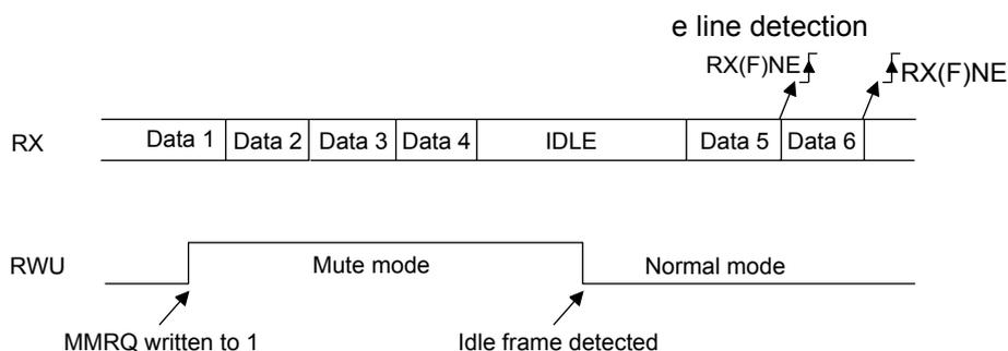
Note: If the MMRQ is set while the IDLE character has already elapsed, mute mode is not entered (RWU is not set). If the LPUART is activated while the line is IDLE, the idle state is detected after the duration of one IDLE frame (not only after the reception of one character frame).
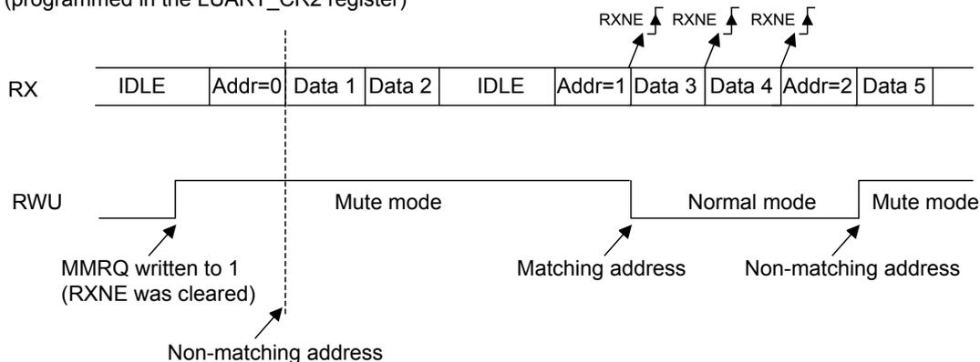
4-bit/7-bit address mark detection (WAKE=1)
In this mode, bytes are recognized as addresses if their MSB is a '1', otherwise they are considered as data. In an address byte, the address of the targeted receiver is put in the 4 or 7 LSBs. The choice of 7 or 4 bit address detection is done using the ADDM7 bit. This 4- bit/7-bit word is compared by the receiver with its own address which is programmed in the ADD bits in the LPUART_CR2 register.
Note: In 7-bit and 9-bit data modes, address detection is done on 6-bit and 8-bit addresses (ADD[5:0] and ADD[7:0]) respectively.
The LPUART enters mute mode when an address character is received which does not match its programmed address. In this case, the RWU bit is set by hardware. The RXNE flag is not set for this address byte and no interrupt or DMA request is issued when the LPUART enters mute mode.
The LPUART also enters mute mode when the MMRQ bit is written to 1. The RWU bit is also automatically set in this case.
The LPUART exits from mute mode when an address character is received which matches the programmed address. Then the RWU bit is cleared and subsequent bytes are received normally. The RXNE/RXFNE bit is set for the address character since the RWU bit has been cleared.
Note: When FIFO management is enabled, when MMRQ bit is set while the receiver is sampling the last bit of a data; this data may be received before effectively entering in mute mode.
An example of mute mode behavior using address mark detection is given in Figure 122. Mute mode using address mark detection.
Figure 144. Mute mode using address mark detection
In this example, the current address of the receiver is 1 (programmed in the LPUART_CR2 register)
21.3.7 Parity control
Parity control (generation of parity bit in transmission and parity checking in reception) can be enabled by setting the PCE bit in the LPUART_CR1 register. Depending on the frame length defined by the M bits, the possible LPUART frame formats are as listed in Table 67. Frame formats .
Table 67. Frame formats
| M bits | PCE bit | LPUART frame (1) |
|---|---|---|
| 00 | 0 | | SB | 8-bit data | STB | |
| 00 | 1 | | SB | 7-bit data | PB | STB | |
| 01 | 0 | | SB | 9-bit data | STB | |
| 01 | 1 | | SB | 8-bit data PB | STB | |
| 10 | 0 | | SB | 7-bit data | STB | |
| 10 | 1 | | SB | 6-bit data | PB | STB | |
1. Legends: SB: start bit, STB: stop bit, PB: parity bit. In the data register the PB is always taking the MSB position (8 th or 7 th , depending on the M bit value).
Even parity
The parity bit is calculated to obtain an even number of “1”s inside the frame which is made of the 6, 7 or 8 LSB bits (depending on M bit values) and the parity bit.
As an example, if data=00110101, and 4 bits are set, then the parity bit is 0 if even parity is selected (PS bit in LPUART_CR1 = 0).
Odd parity
The parity bit is calculated to obtain an odd number of “1”s inside the frame made of the 6, 7 or 8 LSB bits (depending on M bit values) and the parity bit.
As an example, if data=00110101 and 4 bits set, then the parity bit is 1 if odd parity is selected (PS bit in LPUART_CR1 = 1).
Parity checking in reception
If the parity check fails, the PE flag is set in the LPUART_ISR register and an interrupt is generated if PEIE is set in the LPUART_CR1 register. The PE flag is cleared by software writing 1 to the PECF in the LPUART_ICR register.
Parity generation in transmission
If the PCE bit is set in LPUART_CR1, then the MSB bit of the data written in the data register is transmitted but is changed by the parity bit (even number of “1”s if even parity is selected (PS=0) or an odd number of “1”s if odd parity is selected (PS=1)).
21.3.8 Single-wire half-duplex communication
Single-wire half-duplex mode is selected by setting the HDSEL bit in the LPUART_CR3 register.
The LPUART can be configured to follow a single-wire half-duplex protocol where the TX and RX lines are internally connected. The selection between half- and full-duplex communication is made with a control bit HDSEL in LPUART_CR3.
As soon as HDSEL is written to 1:
- • The TX and RX lines are internally connected
- • The RX pin is no longer used
- • The TX pin is always released when no data is transmitted. Thus, it acts as a standard I/O in idle or in reception. It means that the I/O must be configured so that TX is configured as alternate function open-drain with an external pull-up.
Apart from this, the communication protocol is similar to normal LPUART mode. Any conflicts on the line must be managed by software (by the use of a centralized arbiter, for instance). In particular, the transmission is never blocked by hardware and continues as soon as data is written in the data register while the TE bit is set.
Note: As the TX line and the RX lines are connected together, all the transmitted data are stored in the RX FIFO as the data received from an external device. The software has to take care to discard its “own” information after a transmit phase. In half-duplex mode, it is always wise to read back the transmitted data to check if they are correct as there is no hardware protection against possible collision between nodes. If the software does not want to have the RX FIFO storing the transmitted value then it has to disable the receiver part while transmitting (by clearing the RE bit in USART_CR1 register).
Note: In LPUART, in the case of 1-STOP bit configuration, the RXNE flag is set in the middle of the STOP bit.
21.3.9 Continuous communication using DMA
The LPUART is capable of performing continuous communication using the DMA. The DMA requests for Rx buffer and Tx buffer are generated independently.
Note: Refer to Section 20.4: USART implementation to determine if the DMA mode is supported. If DMA is not supported, use the LPUSRT to perform continuous communication. When FIFO is disabled, you can clear the TXE/ RXNE flags in the LPUART_ISR register.
Transmission using DMA
DMA mode can be enabled for transmission by setting DMAT bit in the LPUART_CR3 register. Data is loaded from an SRAM area configured using the DMA peripheral to the LPUART_TDR register whenever the TXE flag (TXFNF flag if FIFO mode is enabled) is set. To map a DMA channel for LPUART transmission, use the following procedure (x denotes the channel number):
- 1. Write the LPUART_TDR register address in the DMA control register to configure it as the destination of the transfer. The data is moved to this address from memory after each TXE (or TXFNF if FIFO mode is enabled) event.
- 2. Write the memory address in the DMA control register to configure it as the source of the transfer. The data is loaded into the LPUART_TDR register from this memory area after each TXE (or TXFNF if FIFO mode is enabled) event.
- 3. Configure the total number of bytes to be transferred to the DMA control register.
- 4. Configure the channel priority in the DMA register.
- 5. Configure DMA interrupt generation after half/full transfer as required by the application.
- 6. Clear the TC flag in the LPUART_ISR register by setting the TCCF bit in the LPUART_ICR register.
- 7. Activate the channel in the DMA register.
When the number of data transfers programmed in the DMA controller is reached, the DMA controller generates an interrupt on the DMA channel interrupt vector.
In transmission mode, once the DMA has written all the data to be transmitted (the TCIF flag is set in the DMA_ISR register), the TC flag can be monitored to make sure that the LPUART communication is complete. This is required to avoid corrupting the last transmission before disabling the LPUART or entering Deepstop mode. Software must wait until TC=1. The TC flag remains cleared during all data transfers and it is set by hardware at the end of transmission of the last frame.
Figure 145. Transmission using DMA
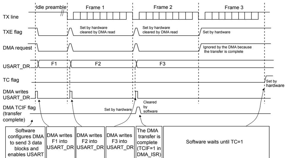
The diagram illustrates the timing for DMA transmission across three frames (Frame 1, Frame 2, Frame 3) following an idle preamble. The signals shown are:
- TX line: Shows the idle preamble followed by the transmission of Frame 1, Frame 2, and Frame 3.
- TXE flag: Set by hardware when the USART_DR register is empty and cleared by a DMA read. It is set before each frame and cleared after the last byte of each frame is transmitted.
- DMA request: Triggered by the TXE flag. It is ignored by the DMA because the transfer is complete after the third frame.
- USART_DR: Shows the data blocks F1, F2, and F3 being written into the register by the DMA.
- TC flag: Set by hardware when the entire frame has been transmitted. It is cleared by software.
- DMA TCIF flag (transfer complete): Set by hardware when the DMA transfer is complete (after the third frame). It is cleared by software.
Below the timing diagram, a sequence of events is shown:
- Software configures DMA to send 3 data blocks and enables USART.
- DMA writes F1 into USART_DR.
- DMA writes F2 into USART_DR.
- DMA writes F3 into USART_DR.
- The DMA transfer is complete (TCIF=1 in DMA_ISR).
- Software waits until TC=1.
Note: When FIFO management is enabled, the DMA request is triggered by transmit FIFO not full (i.e. TXFNF = 1).
Reception using DMA
DMA mode can be enabled for reception by setting the DMAR bit in LPUART_CR3 register. Data is loaded from the LPUART_RDR register to an SRAM area configured using the DMA peripheral whenever a data byte is received. To map a DMA channel for LPUART reception, use the following procedure:
- 1. Write the LPUART_RDR register address in the DMA control register to configure it as the source of the transfer. The data is moved from this address to the memory after each RXNE (RXFNE in case FIFO mode is enabled) event.
- 2. Write the memory address in the DMA control register to configure it as the destination of the transfer. The data is loaded from LPUART_RDR to this memory area after each RXNE (RXFNE in case FIFO mode is enabled) event.
- 3. Configure the total number of bytes to be transferred to the DMA control register.
- 4. Configure the channel priority in the DMA control register.
- 5. Configure interrupt generation after half/full transfer as required by the application.
- 6. Activate the channel in the DMA control register.
When the number of data transfers programmed in the DMA controller is reached, the DMA controller generates an interrupt on the DMA channel interrupt vector.
Figure 146. Reception using DMA
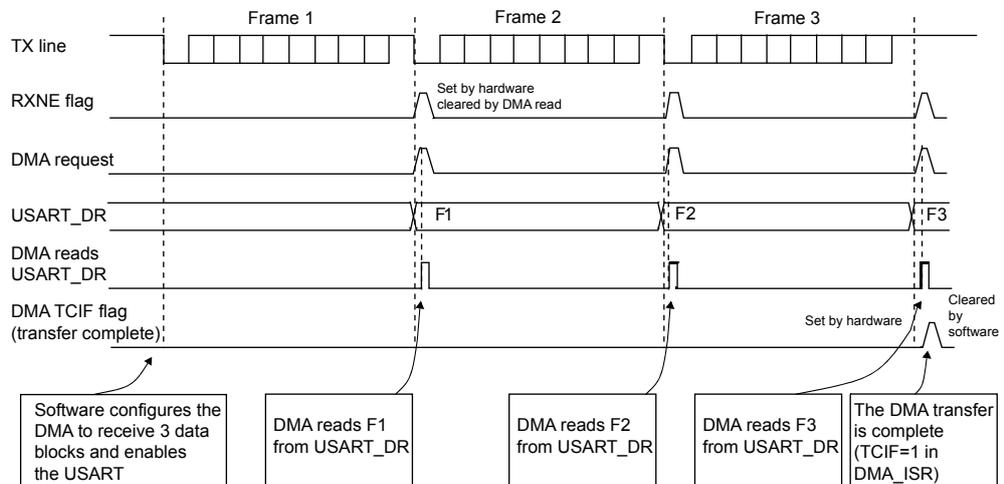
Note: When FIFO management is enabled, the DMA request is triggered by receive FIFO not empty (i.e. RXFNE = 1).
Error flagging and interrupt generation in multibuffer communication
In multibuffer communication if any error occurs during the transaction the error flag is asserted after the current byte. An interrupt is generated if the interrupt enable flag is set. For framing error, overrun error and noise flag which are asserted with RXNE (RXFNE in case FIFO mode is enabled) in single-byte reception, there is a separate error flag interrupt enable bit (EIE bit in the LPUART_CR3 register), which, if set, enables an interrupt after the current byte if any of these errors occur.
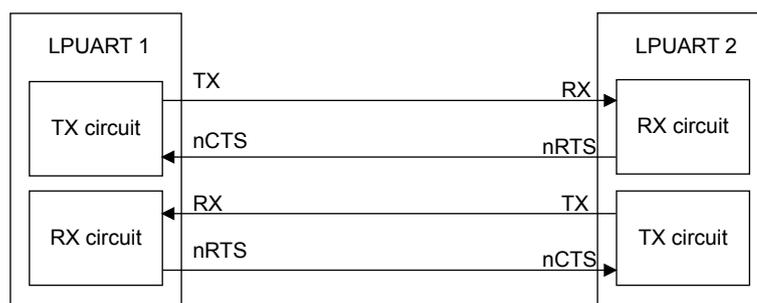
21.3.10 RS232 Hardware flow control and RS485 Driver Enable
It is possible to control the serial data flow between 2 devices by using the nCTS input and the nRTS output. Figure 135. Hardware flow control between 2 USARTs shows how to connect 2 devices in this mode:
Figure 147. Hardware flow control between 2 LPUARTs
RS232 RTS and CTS flow control can be enabled independently by writing the RTSE and CTSE bits respectively to 1 (in the LPUART_CR3 register).
RS232 RTS flow control
If the RTS flow control is enabled (RTSE=1), then nRTS is asserted (tied low) as long as the LPUART receiver is ready to receive a new data. When the receive register is full, nRTS is deasserted, indicating that the transmission is expected to stop at the end of the current frame. Figure 136. RS232 RTS flow control shows an example of communication with RTS flow control enabled.
Figure 148. RS232 RTS flow control
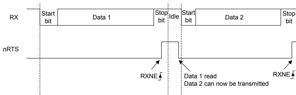
Note: When FIFO mode is enabled, nRTS is deasserted only when RXFIFO is full.
RS232 CTS flow control
If the CTS flow control is enabled (CTSE=1), then the transmitter checks the nCTS input before transmitting the next frame. If nCTS is asserted (tied low), then the next data is transmitted (assuming that data is to be transmitted, in other words, if TXE/TXFE=0), otherwise the transmission does not occur. When nCTS is deasserted during a transmission, the current transmission is completed before the transmitter stops.
When CTSE=1, the CTSIF status bit is automatically set by hardware as soon as then CTS input toggles. It indicates when the receiver becomes ready or not ready for communication.
An interrupt is generated if the CTSIE bit in the LPUART_CR3 register is set. shows an example of communication with CTS flow control enabled.
Figure 149. RS232 RTS flow control
Note: For a correct behavior, nCTS must be asserted at least 3 LPUART clock source periods before the end of the current character. In addition it should be noted that the CTSCF flag may not be set for pulses shorter than 2 x PCLK periods.
RS485 driver enable
The driver enable feature is enabled by setting bit DEM in the LPUART_CR3 control register. This allows the user to activate the external transceiver control through the DE (DriverEnable) signal. The assertion time is the time between the activation of the DE signal and the beginning of the START bit. It is programmed using the DEAT [4:0] bit fields in the LPUART_CR1 control register. The de-assertion time is the time between the end of the last stop bit, in a transmitted message, and the de-activation of the DE signal. It is programmed using the DEDT [4:0] bit fields in the LPUART_CR1 control register. The polarity of the DE signal can be configured using the DEP bit in the LPUART_CR3 control register.
In LPUART, the DEAT and DEDT are expressed in LPUART clock source (f CK ) cycles:
- • The driver enable assertion time=
- – \( (1 + (\text{DEAT} \times P)) \times f_{CK} \) , if \( P \neq 0 \)
- – \( (1 + \text{DEAT}) \times f_{CK} \) , if \( P = 0 \)
- • The driver enable de-assertion time=
- – \( (1 + (\text{DEDT} \times P)) \times f_{CK} \) , if \( P \neq 0 \)
- – \( (1 + \text{DEDT}) \times f_{CK} \) , if \( P = 0 \)
21.4 LPUART interrupts
Table 68. LPUART interrupt requests
| Interrupt event | Event flag | Enable control bit |
|---|---|---|
| Transmit data register empty | TXE | TXEIE |
| Transmit FIFO not full | TXFNF | TXFNFIE |
| Transmit FIFO empty | TXFE | TXFEIE |
| CTS interrupt | CTSIF | CTSIE |
| Transmission complete | TC | TCIE |
| Receive data register not empty (data ready to be read) | RXNE | RXNEIE |
| Receive FIFO not empty | RXFNE | RXFNEIE |
| Receive FIFO full | RXFF | RXFFIE |
| Overrun error detected | ORE | RXNEIE/RXF- NEIE |
| Idle line detected | IDLE | IDLEIE |
| Parity error | PE | PEIE |
| Noise Flag, Overrun error and Framing Error in multi-buffer communication | NF or ORE or FE | EIE |
| Character match | CMF | CMIE |
These events generate an interrupt if the corresponding enable control bit is set.
21.5 LPUART registers
Refer to Section 1.5: Acronyms for a list of abbreviations used in register descriptions.
21.5.1 Control register 1 (LPUART_CR1)
Address offset: 0x00
Reset value: 0x0000
| 31 | 30 | 29 | 28 | 27 | 26 | 25 | 24 | 23 | 22 | 21 | 20 | 19 | 18 | 17 | 16 |
|---|---|---|---|---|---|---|---|---|---|---|---|---|---|---|---|
| RXFFIE | TXFEIE | FIFOEN | M1 | Res. | Res. | DEAT[4:0] | DEDT[4:0] | ||||||||
| rw | rw | rw | rw | rw | rw | rw | rw | rw | rw | rw | rw | rw | rw | ||
| 15 | 14 | 13 | 12 | 11 | 10 | 9 | 8 | 7 | 6 | 5 | 4 | 3 | 2 | 1 | 0 |
| Res. | CMIE | MME | M0 | WAKE | PCE | PS | PEIE | TXEIE TXFNIE | TCIE | RXNEIE RXFNIE | IDLEIE | TE | RE | Res. | UE |
| rw | rw | rw | rw | rw | rw | rw | rw | rw | rw | rw | rw | rw | rw | ||
| Bit 31 | RXFFIE: RXFIFO full interrupt enable. This bit is set and cleared by software. 0: Interrupt is inhibited Note: When FIFO mode is disabled, this bit is reserved and must be kept at reset value. |
| Bit 30 | TXFEIE: TXFIFO empty interrupt enable. This bit is set and cleared by software. 0: Interrupt is inhibited Note: When FIFO mode is disabled, this bit is reserved and must be kept at reset value. |
| Bit 29 | FIFOEN: FIFO mode enable. This bit is set and cleared by software. 0: FIFO mode is disabled |
| Bit 28 | M1: Word length. This bit, with bit 12 (M0) determines the word length. It is set or cleared by software. M[1:0] = 00: 1 start bit, 8 data bits, n stop bit This bit can only be written when the LPUART is disabled (UE=0). Note: in 7-bits data length mode, the Smartcard mode, LIN master mode and auto baud rate (0x7F and 0x55 frames detection) are not supported. |
| Bit 27 | Reserved, must be kept at reset value. |
| Bit 26 | Reserved, must be kept at reset value. |
| Bits 25:21 | DEAT[4:0]: Driver enable assertion time. This 5-bit value defines the time between the activation of the DE (driver enable) signal and the beginning of the start bit. It is expressed in UCLK (LPUART clock) clock cycles. For more details, refer to RS485 driver enable section. This bit field can only be written when the LPUART is disabled (UE=0). |
| Bits 20:16 | DEDT[4:0]: Driver enable de-assertion time. This 5-bit value defines the time between the end of the last stop bit, in a transmitted message, and the de-activation of the DE (Driver Enable) signal. It is expressed in UCLK (LPUART clock) clock cycles. For more details, refer to RS485 driver enable section. If the LPUART_TDR register is written during the DEDT time, the new data is transmitted only when the DEDT and DEAT times have both elapsed. This bit field can only be written when the LPUART is disabled (UE=0). |
| Bit 15 | Reserved, must be kept at reset value. |
| Bit 14 | CMIE: Character match interrupt enable. This bit is set and cleared by software. 0: Interrupt is inhibited 1: An LPUART interrupt is generated when the CMF bit is set in the LPUART_ISR register |
| Bit 13 | MME: Mute mode enable. This bit activates the mute mode function of the LPUART. When set, the LPUART can switch between the active and mute modes, as defined by the WAKE bit. It is set and cleared by software. 0: Receiver in active mode permanently 1: Receiver can switch between mute mode and active mode |
| Bit 12 | M0: Word length. This bit, with bit 28 (M1) determines the word length. It is set or cleared by software. See Bit 28 (M1) description. This bit can only be written when the LPUART is disabled (UE=0). |
| Bit 11 | WAKE: Receiver wakeup method. This bit determines the LPUART wakeup method from mute mode. It is set or cleared by software. 0: Idle line 1: Address mark This bit field can only be written when the LPUART is disabled (UE=0). |
| Bit 10 | PCE: Parity control enable. This bit selects the hardware parity control (generation and detection). When the parity control is enabled, the computed parity is inserted at the MSB position (9th bit if M=1; 8th bit if M=0) and parity is checked on the received data. This bit is set and cleared by software. Once it is set, PCE is active after the current byte (in reception and in transmission). 0: Parity control disabled 1: Parity control enabled This bit field can only be written when the LPUART is disabled (UE=0). |
| Bit 9 | PS: Parity selection. This bit selects the odd or even parity when the parity generation/detection is enabled (PCE bit set). It is set and cleared by software. The parity is selected after the current byte. 0: Even parity 1: Odd parity This bit field can only be written when the LPUART is disabled (UE=0). |
| Bit 8 | PEIE: PE interrupt enable. This bit is set and cleared by software. 0: Interrupt is inhibited 1: An LPUART interrupt is generated whenever PE=1 in the LPUART_ISR register |
| Bit 7 | TXEIE/TXFNIE: Transmit data register empty/TXFIFO not full interrupt enable. This bit is set and cleared by software. 0: Interrupt is inhibited 1: An LPUART interrupt is generated whenever TXE/TXNF=1 in the LPUART_ISR register |
| Bit 6 | TCIE: Transmission complete interrupt enable. This bit is set and cleared by software. 0: Interrupt is inhibited 1: An LPUART interrupt is generated whenever TC=1 in the LPUART_ISR register |
| Bit 5 | RXNEIE/RXFNEIE: Receive data register not empty/RXFIFO not empty interrupt enable. This bit is set and cleared by software. 0: Interrupt is inhibited 1: An LPUART interrupt is generated whenever ORE=1 or RXNE/RXFNE=1 in the LPUART_ISR register |
| Bit 4 | IDLEIE: IDLE interrupt enable. This bit is set and cleared by software. 0: Interrupt is inhibited 1: An LPUART interrupt is generated whenever IDLE=1 in the LPUART_ISR register |
| Bit 3 | TE: Transmitter enable. This bit enables the transmitter. It is set and cleared by software. 0: Transmitter is disabled 1: Transmitter is enabled Note: During transmission, a “0” pulse on the TE bit (“0” followed by “1”) sends a preamble (idle line) after the current word. In order to generate an idle character, the TE must not be immediately written to 1. In order to ensure the required duration, the software can poll the TEACK bit in the LPUART_ISR register. When TE is set there is a 1 bit-time delay before the transmission starts. |
| Bit 2 | RE: Receiver enable. This bit enables the receiver. It is set and cleared by software. 0: Receiver is disabled 1: Receiver is enabled and begins searching for a start bit |
| Bit 1 | Reserved, must be kept at reset value. |
| Bit 0 | UE: LPUART enable. When this bit is cleared, the LPUART prescalers and outputs are stopped immediately, and current operations are discarded. The configuration of the LPUART is kept, but all the status flags, in the LPUART_ISR are reset. This bit is set and cleared by software. 0: LPUART prescaler and outputs disabled, low-power mode 1: LPUART enabled Note: In order to go into low-power mode without generating errors on the line, the TE bit must be reset before and the software must wait for the TC bit in the LPUART_ISR to be set before resetting the UE bit. The DMA requests are also reset when UE = 0 so the DMA channel must be disabled before resetting the UE bit. |
21.5.2 Control register 2 (LPUART_CR2)
Address offset: 0x04
Reset value: 0x0000
| 31 | 30 | 29 | 28 | 27 | 26 | 25 | 24 | 23 | 22 | 21 | 20 | 19 | 18 | 17 | 16 |
|---|---|---|---|---|---|---|---|---|---|---|---|---|---|---|---|
| ADD[7:4] | ADD[3:0] | Res. | Res. | Res. | Res. | MSBFIRST | DATAINV | TXINV | RXINV | ||||||
| rw | rw | rw | rw | rw | rw | rw | rw | rw | rw | rw | rw | ||||
| 15 | 14 | 13 | 12 | 11 | 10 | 9 | 8 | 7 | 6 | 5 | 4 | 3 | 2 | 1 | 0 |
| SWAP | Res. | STOP[1:0] | Res. | Res. | Res. | Res. | Res. | Res. | Res. | ADDM7 | Res. | Res. | Res. | Res. | |
| rw | rw | rw | rw | ||||||||||||
| Bits 31:28 | ADD[7:4]: Address of the LPUART node. This bit-field gives the address of the LPUART node or a character code to be recognized. This is used in multiprocessor communication during mute mode or Deepstop mode, for wakeup with 7- bit address mark detection. The MSB of the character sent by the transmitter should be equal to 1. It may also be used for character detection during normal reception, mute mode inactive (for example, end of block detection in ModBus protocol). In this case, the whole received character (8-bit) is compared to the ADD[7:0] value and CMF flag is set on match. This bit field can only be written when reception is disabled (RE=0) or the LPUART is disabled (UE=0). |
| Bits 27:24 | ADD[3:0]: Address of the LPUART node. This bit-field gives the address of the LPUART node or a character code to be recognized. This is used in multiprocessor communication during Mute mode or Deepstop mode, for wakeup with address mark detection. This bit field can only be written when reception is disabled (RE=0) or the LPUART is disabled (UE=0) |
| Bit 23:20 | Reserved, must be kept at reset value. |
| Bit 19 | MSBFIRST: Most significant bit first. This bit is set and cleared by software. 0: Data is transmitted/received with data bit 0 first, following the start bit 1: Data is transmitted/received with the MSB (bit 7/8) first, following the start bit. This bit field can only be written when the LPUART is disabled (UE=0). |
| Bit 18 | DATAINV: Binary data inversion. This bit is set and cleared by software. 0: Logical data from the data register are sent/received in positive/direct logic. (1=H, 0=L) 1: Logical data from the data register are sent/received in negative/inverse logic. (1=L, 0=H). The parity bit is also inverted. This bit field can only be written when the LPUART is disabled (UE=0). |
| Bit 17 | TXINV: TX pin active level inversion. This bit is set and cleared by software. 0: TX pin signal works using the standard logic levels (VDD =1/idle, Gnd=0/mark) 1: TX pin signal values are inverted. (VDD =0/mark, Gnd=1/idle). This allows the use of an external inverter on the TX line. This bit field can only be written when the LPUART is disabled (UE=0). |
| Bit 16 | RXINV: RX pin active level inversion. This bit is set and cleared by software. 0: RX pin signal works using the standard logic levels (VDD =1/idle, Gnd=0/mark) 1: RX pin signal values are inverted. (VDD =0/mark, Gnd=1/idle). This allows the use of an external inverter on the RX line. This bit field can only be written when the LPUART is disabled (UE=0). |
| Bit 15 | SWAP: Swap TX/RX pins. This bit is set and cleared by software. 0: TX/RX pins are used as defined in standard pinout 1: The TX and RX pins functions are swapped. This allows to work in the case of a cross-wired connection to another UART. This bit field can only be written when the LPUART is disabled (UE=0). |
| Bit 14 | Reserved, must be kept at reset value. |
| Bits 13:12 | STOP[1:0]: STOP bits. These bits are used for programming the stop bits. 00: 1 stop bit 01: Reserved 10: 2 stop bits 11: Reserved This bit field can only be written when the LPUART is disabled (UE=0). |
| Bit 11:5 | Reserved, must be kept at reset value. |
| Bit 4 | ADD7: 7-bit Address Detection/4-bit Address Detection. This bit is for selection between 4-bit address detection or 7-bit address detection. 0: 4-bit address detection 1: 7-bit address detection (in 8-bit data mode) This bit can only be written when the LPUART is disabled (UE=0). Note: In 7-bit and 9-bit data modes, the address detection is done on 6-bit and 8-bit address (ADD[5:0] and ADD[7:0]) respectively. |
| Bits 3:0 | Reserved, must be kept at reset value. |
21.5.3 Control register 3 (LPUART_CR3)
Address offset: 0x08
Reset value: 0x0000
| 31 | 30 | 29 | 28 | 27 | 26 | 25 | 24 | 23 | 22 | 21 | 20 | 19 | 18 | 17 | 16 |
|---|---|---|---|---|---|---|---|---|---|---|---|---|---|---|---|
| TXFTCFG | RXFTIE | RXFTCFG | Res. | TXFTIE | Res. | Res. | Res. | Res. | Res. | Res. | |||||
| rw | rw | rw | rw | ||||||||||||
| 15 | 14 | 13 | 12 | 11 | 10 | 9 | 8 | 7 | 6 | 5 | 4 | 3 | 2 | 1 | 0 |
| DEP | DEM | DDRE | OVRDIS | Res. | CTSIE | CTSE | RTSE | DMAT | DMAR | Res. | Res. | HD SEL | Res. | Res. | EIE |
| rw | rw | rw | rw | rw | rw | rw | rw | rw | rw | rw | |||||
| Bits 31:29 | TXFTCFG: TXFIFO threshold configuration. 000: TXFIFO reaches 1/8 of its depth |
| Bit 28 | RXFTIE: RXFIFO threshold interrupt enable. This bit is set and cleared by software. 0: Interrupt is inhibited |
| Bits 27:25 | RXFTCFG: Receive FIFO threshold configuration. 000: Receive FIFO reaches 1/8 of its depth |
| Bit 24 | Reserved, must be kept at reset value. |
| Bit 23 | TXFTIE: TXFIFO threshold interrupt enable. This bit is set and cleared by software. 0: Interrupt is inhibited |
| Bits 22:16 | Reserved, must be kept at reset value. |
| Bit 15 | DEP: Driver enable polarity selection. 0: DE signal is active high This bit can only be written when the LPUART is disabled (UE=0). |
| Bit 14 | DEM: Driver enable mode. This bit allows the user to activate the external transceiver control through the DE signal. 0: DE function is disabled This bit can only be written when the LPUART is disabled (UE=0). |
| Bit 13 | DDRE : DMA disable on reception error. 0: DMA is not disabled in case of reception error. The corresponding error flag is set but RXNE is kept 0 preventing from overrun. As a consequence, the DMA request is not asserted, so the erroneous data is not transferred (no DMA request), but next correct received data is transferred. 1: DMA is disabled following a reception error. The corresponding error flag is set, as well as RXNE. The DMA request is masked until the error flag is cleared. This means that the software must first disable the DMA request (DMAR = 0) or clear RXNE before clearing the error flag. This bit can only be written when the LPUART is disabled (UE=0). Note: The reception errors are: parity error, framing error or noise error. |
| Bit 12 | OVRDIS : Overrun disable. This bit is used to disable the receive overrun detection. 0: Overrun Error Flag, ORE, is set when received data is not read before receiving new data 1: Overrun functionality is disabled. If new data is received while the RXNE flag is still set the ORE flag is not set and the new received data overwrites the previous content of the LPUART_RDR register. This bit can only be written when the LPUART is disabled (UE=0). Note: This control bit allows checking the communication flow w/o reading the data. |
| Bit 11 | Reserved, must be kept at reset value. |
| Bit 10 | CTSIE : CTS interrupt enable. 0: Interrupt is inhibited 1: An interrupt is generated whenever CTSIF=1 in the LPUART_ISR register |
| Bit 9 | CTSE : CTS enable. 0: CTS hardware flow control disabled 1: CTS mode enabled, data is only transmitted when the nCTS input is asserted (tied to 0). If the nCTS input is de-asserted while data is being transmitted, then the transmission is completed before stopping. If data is written into the data register while nCTS is asserted, the transmission is postponed until nCTS is asserted. This bit can only be written when the LPUART is disabled (UE=0). |
| Bit 8 | RTSE : RTS enable. 0: RTS hardware flow control disabled 1: RTS output enabled, data is only requested when there is space in the receive buffer. The transmission of data is expected to cease after the current character has been transmitted. The nRTS output is asserted (pulled to 0) when data can be received. This bit can only be written when the LPUART is disabled (UE=0). |
| Bit 7 | DMAT : DMA enable transmitter. This bit is set/reset by software. 1: DMA mode is enabled for transmission 0: DMA mode is disabled for transmission |
| Bit 6 | DMAR : DMA enable receiver. This bit is set/reset by software. 1: DMA mode is enabled for reception 0: DMA mode is disabled for reception |
| Bit 5:4 | Reserved, must be kept at reset value. |
| Bit 3 | HDSEL : Half-duplex selection. Selection of single-wire half-duplex mode. 0: Half-duplex mode is not selected 1: Half-duplex mode is selected This bit can only be written when the LPUART is disabled (UE=0). |
| Bit 2:1 | Reserved, must be kept at reset value. |
| Bit 0 | EIE: Error interrupt enable. Error interrupt enable bit is required to enable interrupt generation in case of a framing error, overrun error or noise flag (FE=1 or ORE=1 or NF=1 in the LPUART_ISR register). 0: Interrupt is inhibited 1: An interrupt is generated when FE=1 or ORE=1 or NF=1 in the LPUART_ISR register |
21.5.4 Baud rate register (LPUART_BRR)
This register can only be written when the LPUART is disabled (UE=0). It may be automatically updated by hardware in auto baud rate detection mode.
Address offset: 0x0C
Reset value: 0x0000
| 31 | 30 | 29 | 28 | 27 | 26 | 25 | 24 | 23 | 22 | 21 | 20 | 19 | 18 | 17 | 16 |
| Res. | Res. | Res. | Res. | Res. | Res. | Res. | Res. | Res. | Res. | Res. | Res. | BRR[19:16] | |||
| rw | rw | rw | rw | ||||||||||||
| 15 | 14 | 13 | 12 | 11 | 10 | 9 | 8 | 7 | 6 | 5 | 4 | 3 | 2 | 1 | 0 |
| BRR[15:0] | |||||||||||||||
| rw | rw | rw | rw | rw | rw | rw | rw | rw | rw | rw | rw | rw | rw | rw | rw |
| Bits 31:20 | Reserved, must be kept at reset value. |
| Bits 19:0 | BRR[19:0] |
Note: It is forbidden to write values less than 0x300 in the LPUART_BRR register. Provided that LPUART_BRR must be \( \geq 0x300 \) and LPUART_BRR is 20 bits, care should be taken when generating high baud rates using high f ck values. f ck must be in the range [3 x baud rate ..4096 x baud rate].
21.5.5 Request register (LPUART_RQR)
Address offset: 0x18
Reset value: 0x0000
| 31 | 30 | 29 | 28 | 27 | 26 | 25 | 24 | 23 | 22 | 21 | 20 | 19 | 18 | 17 | 16 |
|---|---|---|---|---|---|---|---|---|---|---|---|---|---|---|---|
| Res. | Res. | Res. | Res. | Res. | Res. | Res. | Res. | Res. | Res. | Res. | Res. | Res. | Res. | Res. | Res. |
| 15 | 14 | 13 | 12 | 11 | 10 | 9 | 8 | 7 | 6 | 5 | 4 | 3 | 2 | 1 | |
| Res. | Res. | Res. | Res. | Res. | Res. | Res. | Res. | Res. | Res. | Res. | TXFRQ | RXFRQ | MMRQ | SBKRQ | Res. |
| w | w | w | w |
| Bits 31:5 | Reserved, must be kept at reset value. |
| Bit 4 | TXFRQ: Transmit data flush request. This bit is used when FIFO mode is enabled. TXFRQ bit is set to flush the whole FIFO. This sets the flag TXFE (TXFIFO empty, bit 23 in the LPUART_ISR register). Note: In FIFO mode, the TXNFN flag is reset during the flush request until TxFIFO is empty in order to ensure that no data is written in the data register. |
| Bit 3 | RXFRQ: Receive data flush request. Writing 1 to this bit clears the RXNE flag. This allows the received data to be discarded without reading it, and avoid an overrun condition. |
| Bit 2 | MMRQ: Mute mode request. Writing 1 to this bit puts the LPUART in mute mode and resets the RWU flag. |
| Bit 1 | SBKRQ: Send break request. Writing 1 to this bit sets the SBKF flag and request to send a BREAK on the line, as soon as the transmit machine is available. Note: In the case the application needs to send the break character following all previously inserted data, including the ones not yet transmitted, the software should wait for the TXE flag assertion before setting the SBKRQ bit. |
| Bit 0 | Reserved, must be kept at reset value. |
21.5.6 Interrupt and status register (LPUART_ISR)
Address offset: 0x1C
Reset value: 0x00C0 (in case FIFO disabled)
Reset value: 0x08000C0 (in case FIFO enabled)
| 31 | 30 | 29 | 28 | 27 | 26 | 25 | 24 | 23 | 22 | 21 | 20 | 19 | 18 | 17 | 16 |
|---|---|---|---|---|---|---|---|---|---|---|---|---|---|---|---|
| Res. | Res. | Res. | Res. | TXFT | RXFT | Res. | RXFF | TXFE | RE ACK | TE ACK | Res. | RWU | SBKF | CMF | BUSY |
| r | r | r | r | r | r | r | r | r | r | ||||||
| 15 | 14 | 13 | 12 | 11 | 10 | 9 | 8 | 7 | 6 | 5 | 4 | 3 | 2 | 1 | 0 |
| Res. | Res. | Res. | Res. | Res. | CTS | CTSIF | Res. | TXE | TC | RXNE | IDLE | ORE | NF | FE | PE |
| r | r | r | r | r | r | r | r | r | r |
| Bits 31:28 | Reserved, must be kept at reset value. |
| Bit 27 | TXFT: TXFIFO threshold flag. This bit is set by hardware when the TXFIFO reaches the programmed threshold in TXFTCFG in LPUARTx_CR3 register, i.e. the TXFIFO contains TXFTCFG empty locations. An interrupt is generated if the TXFTIE bit = 1 (bit 31) in the LPUART_CR3 register. 0: TXFIFO does not reach the programmed threshold |
| Bit 26 | RXFT: RXFIFO threshold flag. This bit is set by hardware when the RXFIFO reaches the programmed threshold in RXFTCFG in LPUARTx_CR3 register, i.e. the Receive FIFO contains RXFTCFG data. An interrupt is generated if the RXFTIE bit = 1 (bit 27) in the LPUART_CR3 register. 0: Receive FIFO does not reach the programmed threshold |
| Bit 25 | Reserved, must be kept at reset value. |
| Bit 24 | RXFF: RXFIFO Full. This bit is set by hardware when RXFIFO is Full. An interrupt is generated if the RXFFIE bit = 1 in the LPUART_CR1 register. 0: RXFIFO is not full |
| Bit 23 | TXFE: TXFIFO empty. This bit is set by hardware when TXFIFO is empty. When the TXFIFO contains at least one data, this flag is cleared. The TXFE flag can also be set by writing 1 to the bit TXFRQ (bit 4) in the LPUART_RQR register. An interrupt is generated if the TXFEIE bit = 1 (bit 30) in the LPUART_CR1 register. 0: TXFIFO is not empty |
| Bit 22 | REACK: Receive enable acknowledge flag. This bit is set/reset by hardware when the Receive Enable value is taken into account by the LPUART. It can be used to verify that the LPUART is ready for reception before entering Deepstop mode. Note: If the LPUART does not support the wakeup from Deepstop feature, this bit is reserved and forced by hardware to '0'. |
| Bit 21 | TEACK: Transmit enable acknowledge flag. This bit is set/reset by hardware, when the Transmit Enable value is taken into account by the LPUART. It can be used when an idle frame request is generated by writing TE=0, followed by TE=1 in the LPUART_CR1 register, in order to respect the TE=0 minimum period. |
| Bit 20 | Reserved, must be kept at reset value. |
| Bit 19 | RWU: Receiver wakeup from mute mode. This bit indicates if the LPUART is in mute mode. It is cleared/set by hardware when a wakeup/mute sequence is recognized. The mute mode control sequence (address or IDLE) is selected by the WAKE bit in the LPUART_CR1 register. When wakeup on IDLE mode is selected, this bit can only be set by software, writing 1 to the MMRQ bit in the LPUART_RQR register. 0: Receiver in active mode Note: If the LPUART does not support the wakeup from Deepstop feature, this bit is reserved and forced by hardware to '0'. |
| Bit 18 | SBKF: Send break flag. This bit indicates that a send break character was requested. It is set by software, by writing 1 to the SBKRQ bit in the LPUART_CR3 register. It is automatically reset by hardware during the stop bit of break transmission. 0: No break character is transmitted |
| Bit 17 | CMF: Character match flag. This bit is set by hardware, when a the character defined by ADD[7:0] is received. It is cleared by software, writing 1 to the CMCF in the LPUART_ICR register. An interrupt is generated if CMIE=1 in the LPUART_CR1 register. 0: No character match detected |
| Bit 16 | BUSY: Busy flag. This bit is set and reset by hardware. It is active when a communication is on-going on the RX line (successful start bit detected). It is reset at the end of the reception (successful or not). 0: LPUART is idle (no reception) |
| Bit 15:11 | Reserved, must be kept at reset value. |
| Bit 10 | CTS: CTS flag. This bit is set/reset by hardware. It is an inverted copy of the status of the nCTS input pin. 0: nCTS line set Note: If the hardware flow control feature is not supported, this bit is reserved and forced by hardware to '0'. |
| Bit 9 | CTSIF: CTS interrupt flag. This bit is set by hardware when the nCTS input toggles, if the CTSE bit is set. It is cleared by software, by writing 1 to the CTSCF bit in the LPUART_ICR register. An interrupt is generated if CTSIE=1 in the LPUART_CR3 register. 0: No change occurred on the nCTS status line Note: If the hardware flow control feature is not supported, this bit is reserved and forced by hardware to '0'. |
| Bit 8 | Reserved, must be kept at reset value. |
| Bit 7 | TXE/TXFNF: Transmit data register empty/TXFIFO not full. When FIFO mode is disabled, TXE is set by hardware when the content of the LPUARTx_TDR register has been transferred into the shift register. It is cleared by a write to the LPUARTx_TDR register. When FIFO mode is enabled, TXFNF is set by hardware when TXFIFO is not full, and so data can be written in the LPUART_TDR. Every write in the LPUART_TDR places the data in the TXFIFO. This flag remains set until the TXFIFO is full. When the TXFIFO is full, this flag is cleared indicating that data can not be written into the LPUART_TDR. Note: The TXFNF is kept reset during the flush request until TXFIFO is empty. After sending the flush request (by setting TXFRQ bit), the flag TXFNF should be checked prior to writing in TXFIFO. (TXFNF and TXFE is set at the same time). An interrupt is generated if the TXEIE/TXFNFIE bit = 1 in the LPUART_CR1 register. 0: Data register is full/Transmit FIFO is full Note: This bit is used during single buffer transmission. |
| Bit 6 | TC: Transmission complete. This bit is set by hardware if the transmission of a frame containing data is complete and if TXE/TXFF is set. An interrupt is generated if TCIE=1 in the LPUART_CR1 register. It is cleared by software, writing 1 to the TCCF in the LPUART_ICR register or by a write to the LPUART_TDR register. An interrupt is generated if TCIE=1 in the LPUART_CR1 register. 0: Transmission is not complete Note: If TE bit is reset and no transmission is on-going, the TC bit is set immediately. |
| Bit 5 | RXNE/RXFNE: Read data register not empty/RXFIFO not empty. RXNE bit is set by hardware when the content of the LPUARTx_RDR shift register has been transferred to the LPUARTx_RDR register. It is cleared by a read to the LPUARTx_RDR register. The RXNE flag can also be cleared by writing 1 to the RXFRQ in the LPUARTx_RQR register. RXFNE bit is set by hardware when the RXFIFO is not empty, and so data can be read from the LPUART_RDR register. Every read of the LPUART_RDR frees a location in the RXFIFO. It is cleared when the RXFIFO is empty. The RXNE/RXFNE flag can also be cleared by writing 1 to the RXFRQ in the LPUART_RQR register. An interrupt is generated if RXNEIE/RXFNEIE=1 in the LPUART_CR1 register. 0: Data is not received |
| Bit 4 | IDLE: Idle line detected. This bit is set by hardware when an idle line is detected. An interrupt is generated if IDLEIE=1 in the LPUART_CR1 register. It is cleared by software, writing 1 to the IDLECF in the LPUART_ICR register. 0: No Idle line is detected Note: The IDLE bit is not set again until the RXNE bit has been set (i.e. a new idle line occurs). If mute mode is enabled (MME=1), IDLE is set if the LPUART is not mute (RWU=0), whatever the mute mode selected by the WAKE bit. If RWU=1, IDLE is not set. |
| Bit 3 | ORE: Overrun error. This bit is set by hardware when the data currently being received in the shift register is ready to be transferred into the LPUARTx_RDR register while RXNE=1 (RXFF=1 in case FIFO mode is enabled). It is cleared by a software, writing 1 to the ORECF, in the LPUARTx_ICR register. An interrupt is generated if RXNEIE/ RXFNEIE=1 or EIE=1 in the LPUARTx_CR1 register. 0: No overrun error Note: When this bit is set, the LPUART_RDR register content is not lost but the shift register is overwritten. An interrupt is generated if the ORE flag is set during multi-buffer communication if the EIE bit is set. This bit is permanently forced to 0 (no overrun detection) when the bit OVRDIS is set in the LPUART_CR3 register. |
| Bit 2 | NF: START bit noise detection flag. This bit is set by hardware when noise is detected on the START bit of a received frame. It is cleared by software, writing 1 to the NFCF bit in the LPUART_ICR register. 0: No noise is detected Note: This bit does not generate an interrupt as it appears at the same time as the RXNE/RXFNE bit which itself generates an interrupt. An interrupt is generated when the NF flag is set during multi buffer communication if the EIE bit is set. Note: In FIFO mode, this error is associated with the character in the LPUART_RDR. |
| Bit 1 | FE: Framing error. This bit is set by hardware when a de-synchronization, excessive noise or a break character is detected. It is cleared by software, writing 1 to the FECF bit in the LPUART_ICR register. In Smartcard mode, in transmission, this bit is set when the maximum number of transmit attempts is reached without success (the card NACKs the data frame). An interrupt is generated if EIE=1 in the LPUART_CR1 register. 0: No framing error is detected Note: In FIFO mode, this error is associated with the character in the LPUART_RDR. |
| Bit 0 | PE: Parity error. This bit is set by hardware when a parity error occurs in receiver mode. It is cleared by software, writing 1 to the PECF in the LPUART_ICR register. An interrupt is generated if PEIE=1 in the LPUART_CR1 register. 0: No parity error Note: In FIFO mode, this error is associated with the character in the LPUART_RDR. |
21.5.7 Interrupt flag clear register (LPUART_ICR)
Address offset: 0x20
Reset value: 0x0000
| 31 | 30 | 29 | 28 | 27 | 26 | 25 | 24 | 23 | 22 | 21 | 20 | 19 | 18 | 17 | 16 |
|---|---|---|---|---|---|---|---|---|---|---|---|---|---|---|---|
| Res. | Res. | Res. | Res. | Res. | Res. | Res. | Res. | Res. | Res. | Res. | WUCF | Res. | Res. | CMCF | Res. |
| w_r0 | w_r0 | ||||||||||||||
| 15 | 14 | 13 | 12 | 11 | 10 | 9 | 8 | 7 | 6 | 5 | 4 | 3 | 2 | 1 | 0 |
| Res. | Res. | Res. | Res. | Res. | Res. | CTSCF | Res. | Res. | TCCF | Res. | IDLECF | ORECF | NECF | FECF | PECF |
| w_r0 | w_r0 | w_r0 | w_r0 | w_r0 | w_r0 | w_r0 |
| Bits 31:21 | Reserved, must be kept at reset value. |
| Bit 20 | WUCF
: Wakeup from Deepstop mode clear flag. Writing 1 to this bit clears the WUF flag in the LPUART_ISR register. Note: If the LPUART does not support the wakeup from Deepstop feature, this bit is reserved and forced by hardware to '0'. |
| Bit 19:18 | Reserved, must be kept at reset value. |
| Bit 17 | CMCF
: Character match clear flag. Writing 1 to this bit clears the CMF flag in the LPUART_ISR register. |
| Bit 16:10 | Reserved, must be kept at reset value. |
| Bit 9 | CTSCF
: CTS clear flag. Writing 1 to this bit clears the CTSIF flag in the LPUART_ISR register. |
| Bit 8:7 | Reserved, must be kept at reset value. |
| Bit 7 | Reserved, must be kept at reset value. |
| Bit 6 | TCCF : Transmission complete clear flag. Writing 1 to this bit clears the TC flag in the LPUART_ISR register. |
| Bit 5 | Reserved, must be kept at reset value. |
| Bit 4 | IDLECF : Idle line detected clear flag. Writing 1 to this bit clears the IDLE flag in the LPUART_ISR register. |
| Bit 3 | ORECF : Overrun error clear flag. Writing 1 to this bit clears the ORE flag in the LPUART_ISR register. |
| Bit 2 | NECF : Noise detected clear flag. Writing 1 to this bit clears the NF flag in the LPUART_ISR register. |
| Bit 1 | FECF : Framing error clear flag. Writing 1 to this bit clears the FE flag in the LPUART_ISR register. |
| Bit 0 | PECF : Parity error clear flag. Writing 1 to this bit clears the PE flag in the LPUART_ISR register. |
21.5.8 Receive data register (LPUART_RDR)
Address offset: 0x24
Reset value: undefined
| 31 | 30 | 29 | 28 | 27 | 26 | 25 | 24 | 23 | 22 | 21 | 20 | 19 | 18 | 17 | 16 |
| Res. | Res. | Res. | Res. | Res. | Res. | Res. | Res. | Res. | Res. | Res. | Res. | Res. | Res. | Res. | Res. |
| 15 | 14 | 13 | 12 | 11 | 10 | 9 | 8 | 7 | 6 | 5 | 4 | 3 | 2 | 1 | 0 |
| Res. | Res. | Res. | Res. | Res. | Res. | Res. | RDR[8:0] | ||||||||
| r | r | r | r | r | r | r | r | r | |||||||
| Bits 31:9 | Reserved, must be kept at reset value. |
| Bits 8:0 | RDR[8:0]: Receive data value Contains the received data character. The RDR register provides the parallel interface between the input shift register and the internal bus (see Figure 113. USART block diagram ). When receiving with the parity enabled, the value read in the MSB bit is the received parity bit. |
21.5.9 Transmit data register (LPUART_TDR)
Address offset: 0x28
Reset value: undefined
| 31 | 30 | 29 | 28 | 27 | 26 | 25 | 24 | 23 | 22 | 21 | 20 | 19 | 18 | 17 | 16 |
| Res. | Res. | Res. | Res. | Res. | Res. | Res. | Res. | Res. | Res. | Res. | Res. | Res. | Res. | Res. | Res. |
| 15 | 14 | 13 | 12 | 11 | 10 | 9 | 8 | 7 | 6 | 5 | 4 | 3 | 2 | 1 | 0 |
| Res. | Res. | Res. | Res. | Res. | Res. | Res. | TDR[8:0] | ||||||||
| rw | rw | rw | rw | rw | rw | rw | rw | rw | |||||||
| Bits 31:9 | Reserved, must be kept at reset value. |
| Bits 8:0 | TDR[8:0]: Transmit data value contains the data character to be transmitted. The TDR register provides the parallel interface between the internal bus and the output shift register (see Figure 113. USART block diagram ). When transmitting with the parity enabled (PCE bit set to 1 in the LPUART_CR1 register), the value written in the MSB (bit 7 or bit 8 depending on the data length) has no effect because it is replaced by the parity. Note: This register must be written only when TXE/TXFNF=1. |
21.5.10 Prescaler register (LPUART_PRESC)
This register can only be written when the USART is disabled (UE=0).
Address offset: 0x2C
Reset value: 0x0000
| 31 | 30 | 29 | 28 | 27 | 26 | 25 | 24 | 23 | 22 | 21 | 20 | 19 | 18 | 17 | 16 |
| Res. | Res. | Res. | Res. | Res. | Res. | Res. | Res. | Res. | Res. | Res. | Res. | Res. | Res. | Res. | Res. |
| 15 | 14 | 13 | 12 | 11 | 10 | 9 | 8 | 7 | 6 | 5 | 4 | 3 | 2 | 1 | 0 |
| Res. | Res. | Res. | Res. | Res. | Res. | Res. | Res. | Res. | Res. | Res. | Res. | PRESCALER[3:0] | |||
| rw | rw | rw | rw | ||||||||||||
| Bits 31:4 | Reserved, must be kept at reset value. |
| Bits 3:0 | PRESCALER[3:0]: Clock prescaler. The USART input clock can be divided by a prescaler:
Remaining combinations: Reserved. Note: When PRESCALER is programmed with a value different of the allowed ones, programmed prescaler value is «1011», i.e. input clock divided by 256. |
21.5.11 LPUART register map
The table below gives the LPUART register map and reset values.
Table 69. LPUART register map and reset values
| Offset | Register | 31 | 30 | 29 | 28 | 27 | 26 | 25 | 24 | 23 | 22 | 21 | 20 | 19 | 18 | 17 | 16 | 15 | 14 | 13 | 12 | 11 | 10 | 9 | 8 | 7 | 6 | 5 | 4 | 3 | 2 | 1 | 0 | |
|---|---|---|---|---|---|---|---|---|---|---|---|---|---|---|---|---|---|---|---|---|---|---|---|---|---|---|---|---|---|---|---|---|---|---|
| 0x00 | LPUART_CR1 | RXFFIE | TXFEIE | FIFOEN | M1 | Res. | Res. | DEAT[4:0] | DEDT[4:0] | Res. | CMIE | MME | M0 | WAKE | PCE | PS | PEIE | TXEIE | TCIE | RXNEIE | IDLEIE | TE | RE | Res. | UE | |||||||||
| Reset value | 0 | 0 | 0 | 0 | 0 | 0 | 0 | 0 | 0 | 0 | 0 | 0 | 0 | 0 | 0 | 0 | 0 | 0 | 0 | 0 | 0 | 0 | 0 | 0 | 0 | 0 | 0 | 0 | 0 | |||||
| 0x04 | LPUART_CR2 | ADD[7:4] | ADD[3:0] | Res. | Res. | Res. | Res. | MSBFIRST | DATAINV | TXINV | RXINV | SWAP | Res. | STOP [1:0] | Res. | Res. | Res. | Res. | Res. | Res. | Res. | Res. | ADD7 | Res. | Res. | Res. | Res. | |||||||
| Reset value | 0 | 0 | 0 | 0 | 0 | 0 | 0 | 0 | 0 | 0 | 0 | 0 | 0 | 0 | 0 | 0 | ||||||||||||||||||
| 0x08 | LPUART_CR3 | TXFTCF G[2:0] | RXFTIE | RXFTCF G[2:0] | Res. | TXFTIE | Res. | Res. | Res. | Res. | Res. | Res. | Res. | DEP | DEM | DDRE | OVRDIS | Res. | CTSIE | CTSE | RTSE | DMAT | DMAR | Res. | Res. | HDSEL | Res. | Res. | EIE | |||||
| Reset value | 0 | 0 | 0 | 0 | 0 | 0 | 0 | 0 | 0 | 0 | 0 | 0 | 0 | 0 | 0 | 0 | 0 | 0 | 0 | |||||||||||||||
| 0x0C | LPUART_BRR | Res. | Res. | Res. | Res. | Res. | Res. | Res. | Res. | Res. | Res. | Res. | Res. | BRR[19:0] | ||||||||||||||||||||
| Reset value | 0 | 0 | 0 | 0 | 0 | 0 | 0 | 0 | 0 | 0 | 0 | 0 | 0 | 0 | ||||||||||||||||||||
| 0x10- 0x14 | Reserved | |||||||||||||||||||||||||||||||||
| 0x18 | LPUART_RQR | Res. | Res. | Res. | Res. | Res. | Res. | Res. | Res. | Res. | Res. | Res. | Res. | Res. | Res. | Res. | Res. | Res. | Res. | Res. | Res. | Res. | Res. | Res. | Res. | Res. | Res. | Res. | Res. | TXFRQ | RXFRQ | MMRQ | SBKRQ | Res. |
| Reset value | 0 | 0 | 0 | 0 | ||||||||||||||||||||||||||||||
| 0x1C | LPUART_ISR | Res. | Res. | Res. | Res. | Res. | Res. | Res. | Res. | Res. | REACK | TEACK | WUF | RWU | SBKF | CMF | BUSY | Res. | Res. | Res. | Res. | Res. | CTS | CTSIF | Res. | TXE | TC | RXNE | IDLE | ORE | NF | FE | PE | |
| Reset value | 0 | 0 | 0 | 0 | 0 | 0 | 0 | 0 | 0 | 1 | 0 | 0 | 0 | 0 | 0 | 0 | 0 | |||||||||||||||||
| 0x20 | LPUART_ICR | Res. | Res. | Res. | Res. | Res. | Res. | Res. | Res. | Res. | Res. | Res. | WUCF | Res. | Res. | CMCF | Res. | Res. | Res. | Res. | Res. | Res. | Res. | CTSCF | Res. | Res. | TCCF | Res. | IDLECF | ORECF | NECF | FECF | PECF | |
| Reset value | 0 | 0 | 0 | 0 | 0 | 0 | 0 | 0 | 0 | |||||||||||||||||||||||||

| Offset | Register | 31 | 30 | 29 | 28 | 27 | 26 | 25 | 24 | 23 | 22 | 21 | 20 | 19 | 18 | 17 | 16 | 15 | 14 | 13 | 12 | 11 | 10 | 9 | 8 | 7 | 6 | 5 | 4 | 3 | 2 | 1 | 0 | |
|---|---|---|---|---|---|---|---|---|---|---|---|---|---|---|---|---|---|---|---|---|---|---|---|---|---|---|---|---|---|---|---|---|---|---|
| 0x24 | LPUART_RDR | Res. | Res. | Res. | Res. | Res. | Res. | Res. | Res. | Res. | Res. | Res. | Res. | Res. | Res. | Res. | Res. | Res. | Res. | Res. | Res. | Res. | Res. | Res. | Res. | RDR[8:0] | ||||||||
| Reset value | ||||||||||||||||||||||||||||||||||
| 0x28 | LPUART_TDR | Res. | Res. | Res. | Res. | Res. | Res. | Res. | Res. | Res. | Res. | Res. | Res. | Res. | Res. | Res. | Res. | Res. | Res. | Res. | Res. | Res. | Res. | Res. | Res. | TDR[8:0] | ||||||||
| Reset value | ||||||||||||||||||||||||||||||||||
| 0x2C | LPUART_PRESC | Res. | Res. | Res. | Res. | Res. | Res. | Res. | Res. | Res. | Res. | Res. | Res. | Res. | Res. | Res. | Res. | Res. | Res. | Res. | Res. | Res. | Res. | Res. | Res. | Res. | Res. | Res. | Res. | Res. | PRESCALER[3:0] | |||
Refer to Table 3. STM32WB07xC and STM32WB06xC memory map and peripheral register boundary addresses.