12. Analog digital converter (ADC)
The STM32WB07xC and STM32WB06xC embed a 12-bit ADC. The ADC consists of a 12-bit successive approximation analog-to-digital converter (SAR) with 2 x 8 multiplexed channels allowing measurements of up to eight external sources and up to two internal sources.
12.1 Features
- • Conversion frequency is up to 1 Msps
- • Three input voltage ranges are supported (0 → 1.2 V, 0 → 2.4 V, 0 → 3.6 V)
- • Up to eight analog single-ended channels or four analog differential inputs or a mix of both
- • One analog microphone supported through two GPIOs configured in analog mode (an input for the analog microphone and a Vbias output for the analog microphone)
- • Temperature sensor conversion
- • Battery level conversion up to 3.6 V
- • Continuous or single acquisition
- • Digital decimation filter to process a digital audio PDM stream provided by 2 GPIOs and for ADC post-processing, especially for analog audio stream
- • Five modes of conversion are possible:
- – ADC continuous or single mode
- – Analog continuous audio mode
- – Occasional conversions
- – Digital continuous audio mode
- – Full mode
- • ADC down sampler for multi-purpose applications to improve analog performance while off-loading the CPU (ratio adjustable from 1 to 128)
- • A watchdog feature to inform when data is outside thresholds (available for all modes except the digital audio mode)
- • DMA capability
- • Interrupt sources with flags.
12.2 ADC presentation
Figure 22. ADC top level diagram shows the top level diagram of the ADC.
The analog ADC can be configured to interface with the following inputs:
- • External signals through ADC_VINPx and ADC_VINMx, where x=0,1,2 or 3
- – Up to 4 differential inputs
- – Up to 8 single-ended inputs
- • Analog microphone interface
- • Temperature sensor battery level detector up to 3.6 V
- • Battery level detector up to 3.6 V
Figure 22. ADC top level diagram
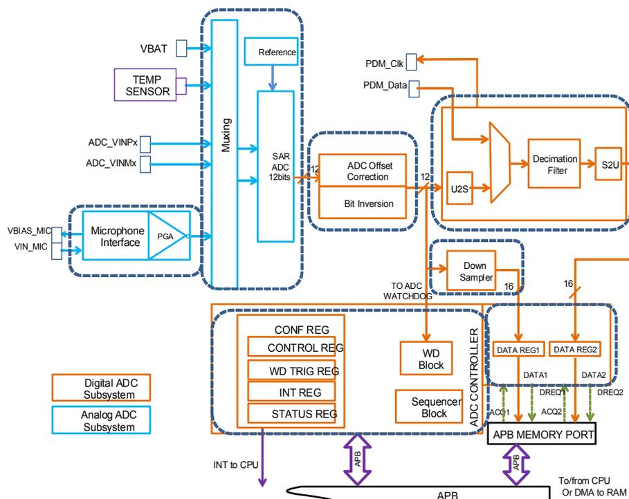
The diagram illustrates the internal architecture of the ADC. On the left, external inputs include VBAT, TEMP SENSOR, ADC_VINPx, and ADC_VINMx. A Microphone Interface with a PGA takes VBIAS_MIC and VIN_MIC as inputs. These signals are routed through a Muxing block to a SAR ADC 12bits. The SAR ADC output (12 bits) passes through an ADC Offset Correction and Bit inversion block. From there, the data path splits: one path goes through a U2S block to a Decimation Filter and then to an S2U block; the other path goes through a Down Sampler (16 bits) to the ADC WATCHDOG. Both paths then enter the ADC CONTROLLER. The controller contains several registers: CONF REG, CONTROL REG, WD TRIG REG, INT REG, and STATUS REG, as well as a WD Block and a Sequencer Block. The controller is connected to an APB MEMORY PORT, which in turn connects to an APB bus. The APB bus is connected to a CPU (INT to CPU) and to DMA to RAM (To/from CPU Or DMA to RAM). A legend indicates that orange boxes represent the Digital ADC Subsystem and blue boxes represent the Analog ADC Subsystem.
In parallel of the analog ADC, a digital microphone can be supported (PDM interface through two GPIOs).
The input of the data path can come from:
- • the analog ADC
- • a digital microphone signal
The conversion data path can go through:
- • a decimation filter
- • a down sampler (for static or low frequency input signals)
The existence of those two different data paths allows some concurrent conversion (specific combinations).
Caution: Do not change the configuration registers related to the function in use. Any change done by the user on the different bits are applied immediately, with an immediate effect on the on-going process (conversion, decimator filter or downsampler). This action can lead to unexpected results.
For VBAT < 2.7 V, the IO booster needs to be activated to maintain linearity.
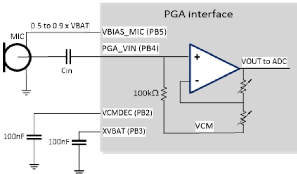
12.2.1 Programmable gain amplifier (PGA)
The input signal coming from the analog microphone is amplified with a programmable gain amplifier (PGA) (see Figure 23. Microphone setup) from 0 dB to 30 dB by step of 3 dB.
The signal is then filtered by a low-pass filter with -1 dB at 20 kHz.
The PGA output voltage is 1.2 V and is inverted versus the VIN_MIC input signal.
Figure 23. Microphone setup
graph LR
    MIC((MIC)) --|Cin| PGA_VIN
    VBIAS_MIC -- 0.5 to 0.9 x VBAT --> MIC
    subgraph PGA_interface
        PGA_VIN(PGA_VIN PB4) --- R1[100kΩ]
        R1 --- OP_IN_POS[+]
        VCMDEC(VCMDEC PB2) --- C1[100nF]
        XVBAT(XVBAT PB3) --- C2[100nF]
        C1 --- GND
        C2 --- GND
        OP_IN_NEG[-] --- VCM
        OP_OUT[VOUT to ADC]
    end
VBIAS_MIC, whose function is independent of PGA_VIN, is used as the microphone power supply. In order to accommodate different microphone supply specifications with a battery that could vary between 1.7 V and 3.6 V, VBIAS_MIC voltage is adjustable as a ratio of VBAT, between 0.5 and 0.9. Refer to the section on PGA_CONF registers for details.
100 nF capacitors need to be connected to VCMDEC and XVBAT respectively to filter out the noise above 1 kHz.
PGA_VIN has a typical input common-mode voltage, VCM, of 750 mV. In order to avoid DC conflicts which could cause saturation in the PGA, a coupling capacitor, Cin, needs to be connected between the microphone and PGA_VIN. The recommended value is 1 µF but one could use a lower value (see Table 30. PGA parameters ). The smaller the capacitor, the quicker the start-up time but with the drawback of the input signal being attenuated. For example, with a Cin of 10 nF a 1 kHz signal would be attenuated by approximately 1 dB.
The PGA gain is adjustable between 0 dB and 30 dB in steps of 3 dB (see Section 12.6.5: ADC PGA configuration register (PGA_CONF) ). In order to avoid distortion in the PGA, the gain setting would need to be adjusted in accordance with the microphone output peak voltage. Below are the PGA maximum output peak voltage values to be respected along with the formula for estimating the maximum PGA gain with respect to the microphone sensitivity, S 0 .
Table 30. PGA parameters
| Parameter | Symbol | Min. | Typ. | Units | Remarks |
|---|---|---|---|---|---|
| Cin | Cin | 0.1 | 1 | µF | 1 µF is recommended |
| PGA Max Vout | MxVout | -6.8 | -5.8 | dBVpk | Typ. at 25 °C; Min. at 105 °C |
Note: \( \text{Maximum PGA gain in dB} = \text{MxVout} - S_0 - 3 \) [N.B. Sensitivity for analog mics are in dBVrms]
Note: E.g. With the microphone sensitivity = -38 dB in a typical setting and no attenuation in the input signal: \( \text{Maximum PGA gain} = -5.8 + 38 - 3 = 29.2 \text{ dB} \) .
Note: The usage of the PGA in analog audio mode implies connecting 3 external capacitors on PB2/PB3/PB4 I/Os. The user has to ensure that the analog switch is well configured to select the PGA external capacitor mode (see Section 8.2.11: I/O analog switch control register (GPIO_SWA_CTRL) for details) and then that those two pads are programmed in analog mode (see Section 7.4.1: GPIO port mode register (GPIOx_MODER) (x = A, B) for details) in this order. A filter needs to be added to the output of the decimation filter in order to filter out the DC level.
12.2.2 Temperature sensor subsystem
The temperature sensor can be used to measure the junction temperature ( \( T_j \) ) of the device. The temperature sensor is internally connected to the ADC input channels which are used to convert the sensor output voltage to a digital value.
The temperature sensor needs to be enabled through the PWRC_CR2.ENTS bit.
The temperature sensor measurement conversion is on the input range 0 to 1.2 V as the temperature range is:
- • for minimum temperature = \( -40\text{ }^\circ\text{C} \) , \( V_{min} = 0.585\text{ V} \)
- • for maximum temperature = \( +125\text{ }^\circ\text{C} \) , \( V_{max} = 0.999\text{ V} \)
The temperature sensor output voltage changes linearly with temperature. The offset of this line varies from chip-to-chip due to process variation. The uncalibrated internal temperature sensor is more suited for applications that detect temperature variations instead of absolute temperatures. To improve the accuracy of the temperature sensor measurement, calibration values are stored in system memory for each device by ST during production. During the manufacturing process, the calibration data of the temperature sensor and the internal voltage reference are stored in the system memory area. The user application can then read them and use them to improve the accuracy of the temperature sensor or the internal reference. In this way the temperature can be calculated with this formula:
Where:
C85 is the temperature sensor calibration value acquired at \( 85\text{ }^\circ\text{C} \) readable @0x10001E68.
C30 is the temperature sensor calibration value acquired at \( 30\text{ }^\circ\text{C} \) readable @0x10001E60.
Cmeas is the actual temperature sensor output value converted by ADC.
Note: ADC gain calibration for VINPx range 1.2 V only must be applied. Offset calibration must be 0 (not used).
Note: Refer to Section 25.1: DESIG registers for information about the location where these calibration values are stored.
12.2.3 Battery sensor
The battery sensor can be used to measure the internal battery voltage of the device. The battery input is internally connected to the ADC input channels which are used to convert the sensor output voltage to a digital value.
The battery sensor range is up to 3.6 V.
The formula for ADC converted data after calibration is the following:
Code = Integer(4096/3.6 * VIN) [clamped at 4095]
As calibration points the VBAT is considered as single negative input with 3.6 V range.
Note: Refer to Section 25.1: DESIG registers for information about the location where these calibration values are stored.
12.2.4 ADC input mode conversion
The ADC is designed to deliver a digital value corresponding to the ratio between the analog power supply and the voltage applied on the converted channel. For most application use cases, it is necessary to convert this ratio into a voltage independent of VDDA.
The formula for ADC digital converted data after calibration and offset is the following:
- • Single-ended input mode
Code = Integer(Slope* VIN) [clamped at 4095]
where Slope for single-ended input mode has the following value:
3.6 V mode: Slope = 4096/3.6 [calibrated gain = 1/3]
2.4 V mode: Slope = 4096/2.4 [calibrated gain = 1/2]
1.2 V mode: Slope = 4096/1.25 [calibrated gain = 0.96, gain clamped at 1]
- • Differential input mode
Code = \( Integer(Slope \cdot (VINP - VINN)) + 2048 \) [clamped at 4095]
where Slope for differential input mode has the following value:
3.6 V mode: Slope = 2048/3.6 [calibrated gain = 1/3]
2.4 V mode: Slope = 2048/2.4 [calibrated gain = 1/2]
1.2 V mode: Slope = 2048/1.25 [calibrated gain = 0.96, gain clamped at 1]
12.2.5 Calibration points
Calibration values are stored in the system memory for each device by ST during production. Each value consists of a 12-bit unsigned value for the gain and an 8-bit signed value for the offset as follows:
OFFSET[18:12] | GAIN[11:0]
These values can be written inside the registers COMP_x with x=1, 2, 3, 4 to apply a point to a particular ADC input. The COMP_SEL register allows a specific calibration point to be associated to one of the ADC inputs.
The offset value can be written inside the COMP_x register only if it fits in the 7-bit of register field, that means offset is in [-64, 63]. Otherwise, it can be removed by the output raw data manually as raw_value + offset.
The negative offset values need to be converted as:
offset | 0x80, if the bitfield BIT_INVERT_SN=1 (default value).
Below the list of the calibration points and their location in the system memory.
Table 31. Calibration points
| Calibration point | Address location |
|---|---|
| VINPx - VINMx range 1.2 V | 0x10001E00 |
| VINMx range 1.2 V | 0x10001E04 |
| VINPx range 1.2 V | 0x10001E08 |
| VINPx - VINMx range 2.4 V | 0x10001E0C |
| VINMx range 2.4 V | 0x10001E10 |
| VINPx range 2.4 V | 0x10001E14 |
| VINPx - VINMx range 3.6 V | 0x10001E18 |
| VINMx range 3.6 V | 0x10001E1C |
| VINPx range 3.6 V | 0x10001E20 |
Note: Previous version of the calibration points has the offset in 7-bit signed. This version can be recognized as the user can read at address 0x10001EFC the value 0.
Note: Refer to Section Section 25.1: DESIG registers for information about the location where these calibration values are stored.
12.2.6 Steady-state input impedance
As the input nature of the ADC is a switched-capacitor, its steady-state input impedance is defined as the impedance seen in DC. It depends only on the analog sampling frequency, Fs, and the input capacitor, Cin: \( Z_{in} = 1/(C_{in} \cdot F_s) \) .
12.2.7 Input signal sampling transient response
As represented in Figure 25. Effect of analog source resistance , the analog signal path consists of a series resistance (Rext) between source and pin, the internal switch resistor (Rin) and the internal sampling capacitor (Cin). The charging of the capacitor is controlled by Rin. When there is Rext in series, the effective value of charging of Cin is governed by Rin+Rext. So the charging time constant becomes (Rin+Rext)*Cin and the necessary time to reach a given accuracy is longer. The ADC has a fixed sampling time Tsw depending on ADC frequency which is 1/Ts as shown in Figure 24. ADC sampling time Tsw and sampling period Ts .
Figure 24. ADC sampling time Tsw and sampling period Ts
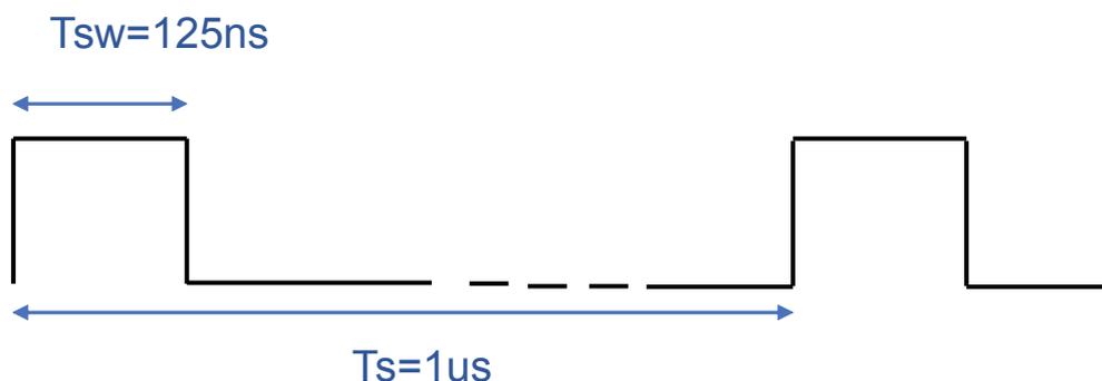
Figure 25. Effect of analog source resistance
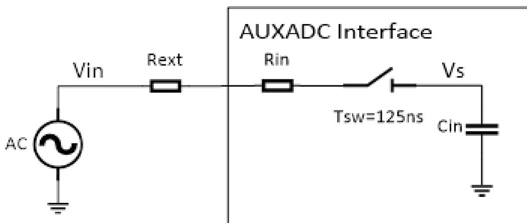
Knowing that: \( R_{in}=550\ \Omega \) , \( C_{in}=4\ pF \) , and imposing a maximum sampling error of 1/2 bits, we can determine the maximum input resistance as below:
where:
12.2.8 Decimation filter (DF)
The purpose of the decimation filter (DF) is to provide a way to reduce the incoming fixed rate sample to some fixed output data rates, while improving the overall noise performance (signal to noise ratio).
The decimation filter is used to process either the PDM data stream from a digital MEMS microphone or from the output of the 12-bit ADC, mainly targeting the audio sources of signal.
The input data rate of the decimation filter is:
- in analog audio / full mode: 1 Mpbs
- in digital audio mode: the PDM clock rate itself (configured through PDM_RATE bit field of the DF_CONF register). The constraint is to fit the MEMS microphone range of possible frequencies (typically 1 to 3 MHz). The decimation filter is composed of two chained blocks:
- a CIC filter capable to perform a wide range of decimation factors
- a FIR filter performing the last stage of decimation and compensating the attenuation effect of the CIC filter.
The FIR filter has a fixed decimation rate of 3
Figure 26. Simplified decimation filter block diagram
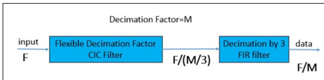
graph LR
    Input[input F] --> CIC[Flexible Decimation Factor CIC Filter]
    CIC --> Intermediate["F/(M/3)"]
    Intermediate --> FIR[Decimation by 3 FIR filter]
    FIR --> Output[data F/M]
    subgraph Decimation Factor=M
    CIC
    FIR
    end
Table 32. Output data rate with ADC input at 1 MHz for analog mode and Table 33. CIC filter output frequency with digital microphone input list the decimation factors and the output frequencies according to the supported inputs (ADC or digital microphone).
The relationship between input data rate and output data rate is that the input data rate is:
- divided by DF_CIC_DEC_FACTOR
- then divided by 3
- divided by 2 if DF_CIC_DHF is set
Note: This divider by 2 is too noisy for digital audio scenario; to be kept for analog scenarios only.
- multiplied by 1.2 if DF_ITP1P2 is set
Table 32. Output data rate with ADC input at 1 MHz for analog mode
| Target frequency | DF_CIC_DEC_FACTOR | DF_CIC_DHF (freq / 2) | DF_ITP1P2 (freq x 1.2) | Output frequency | Error |
|---|---|---|---|---|---|
| 8 kHz | 42 | 0 | 0 | 7.936 kHz | 0.79 % |
| 16 kHz | 21 | 0 | 0 | 15.873 kHz | 0.79 % |
| 200 kHz (1) | 2 | 0 | 1 | 200 kHz | 0 % |
| 44.1 kHz (2) | 14 | 1 | 0 | 44.444 kHz | 0.78 % |
| 48 kHz (2) | 7 | 0 | 0 | 47.619 kHz | 0.79 % |
| 22.05 kHz (2) | 15 | 0 | 0 | 22.222 kHz | 0.78 % |
1. The 200 kHz use-case is not supposed to be used for the analog audio scenario. It mainly targets sensor measurements.
2. This is a possible configuration but neither verified nor guaranteed (to be validated in lab).
Note: A constraint on the ratio between APB system clock (F PCLK ) and the output data rate (DR out ) must be respected:
- In analog audio mode and in full mode, the ratio to respect is \( F_{PCLK} / DR_{out} \geq 6 \) .
Example: F PCLK must be at least 2 MHz to have a DR out = 200 kHz.
If the DMA is not used to get the data output by the decimation filter path, the CPU needs to be clocked at a frequency ratio high enough (taking into account bus matrix latency) to avoid missing samples.
Table 33. CIC filter output frequency with digital microphone input
| Division ratio from 32 MHz clock | Digital microphone frequency | MCIC | Target frequency | Output frequency | Error |
|---|---|---|---|---|---|
| 16 | 2 MHz | 84 | 8 kHz | 7.936 kHz | 0.79 % |
| Division ratio from 32 MHz clock | Digital microphone frequency | MCIC | Target frequency | Output frequency | Error |
|---|---|---|---|---|---|
| 16 | 2 MHz | 42 | 16 kHz | 15.873 kHz | 0.79 % |
| 16 | 2 MHz | 30 | 22.05 kHz | 22.22 kHz | 0.78 % |
| 16 | 2 MHz | 15 | 44.1 kHz | 44.44 kHz | 0.78 % |
| 16 | 2 MHz | 14 | 48 kHz | 47.619 kHz | 0.79 % |
Table 34. Minimum decimation factor for the CIC / total versus pdm_rate provides the value of the allowable minimum decimation factor for the CIC filter and for the complete chain versus the pdm_rate input parameter.
Table 34. Minimum decimation factor for the CIC / total versus pdm_rate
| pdm_rate | Decimation filter input rate | Minimum allowed decimation factor CIC / total |
|---|---|---|
| 0 | 3.2 MHz | 5 / 15 |
| 1 | 2.91 MHz | 5 / 15 |
| 2 | 2.66 MHz | 5 / 15 |
| 3 | 2.46 MHz | 4 / 12 |
| 4 | 2.28 MHz | 4 / 12 |
| 5 | 2.13 MHz | 4 / 12 |
| 6 | 2.00 MHz | 4 / 12 |
| 7 | 1.88 MHz | 3 / 9 |
| 8 | 1.78 MHz | 3 / 9 |
| 9 | 1.68 MHz | 3 / 9 |
| 10 | 1.60 MHz | 3 / 9 |
| 11 | 1.52 MHz | 3 / 9 |
| 12 | 1.46 MHz | 3 / 9 |
| 13 | 1.40 MHz | 3 / 9 |
| 14 | 1.33 MHz | 3 / 9 |
| 15 | 1.28 MHz | 2 / 6 |
When the input of the decimation filter comes from 12-bit ADC, an unsigned-to-signed data conversion is possible through a configuration bit (DF_I_U2S bit in DF_CONF register).
The output of the decimation filter can also be converted from signed to unsigned through a configuration bit (DF_O_S2U bit in DF_CONF register) to be compatible with the down sampler output which is always signed.
The input PDM data is sampled either on the falling edge or the rising edge of the PDM clock. This is configurable through DF_MICRO_L_RN bit in the DF_CONF register. The PDM clock is generated by a division of the decimation filter clock (always 32 MHz) according to the targeted output frequency.
12.2.9 Down sampler (DS)
This down sampler is a simple averaging filter, which can divide the ADC frequency by 1 to 128 by power of 2. The goal is to handle multiple ADC samples and average them into a single data with increased data width ranging from 12-bit to 16-bit.
The down sampler increases the data precision but reduces the output data rate.
Note: A constraint on the ratio between APB system clock ( \( F_{PCLK} \) ) and the output data rate ( \( DR_{out} \) ) must be respected:
- • In ADC mode, the ratio to respect is \( F_{PCLK} / DR_{out} \geq 4 \) .
Example: \( F_{PCLK} \) must be at least 2 MHz to have a \( DR_{out} = 500 \) kHz.
If the DMA is not used to get the data output by the down sampler filter path, the CPU needs to be clocked at a frequency ratio high enough (taking into account bus matrix latency) to avoid missing samples.
12.3 Interrupts
There are 6 maskable interrupts generated by the ADC block. These interrupts are combined to produce one single interrupt output, which is the only interrupt line from the ADC to the CPU.
Table 35. ADC interrupt requests
| Interrupt event | Event flag | Interrupt / flag clearing method | Interrupt enable control bit |
|---|---|---|---|
| Down sampler end of conversion | EODS_IRQ | Write 1 on EODS_IRQ bit | EODS_IRQ_ENA |
| Decimation filter end of conversion | EODF_IRQ | Write 1 on EODF_IRQ bit | EODF_IRQ_ENA |
| End of conversion sequence | EOS_IRQ | Write 1 on EOS_IRQ bit | EOS_IRQ_ENA |
| Analog watchdog event | AWD_IRQ | Write 1 on AWD_IRQ bit | AWD_IRQ_ENA |
| Down sampler overrun | OVR_DS_IRQ | Write 1 on OVR_DS_IRQ bit | OVR_DS_IRQ_ENA |
| Decimation filter overrun | OVR_DF_IRQ | Write 1 on OVR_DF_IRQ bit | OVR_DF_IRQ_ENA |
12.4 DMA interface
The ADC has two DMA channels interface:
- • one to get down sampler data output value (DS_DATAOUT register),
- • one to get Decimation Filter data output value (DF_DATAOUT register)
The DMA feature is enabled by software through CONF register respectively by DMA_DS_ENA bit for down sampler data output and DMA_DF_ENA bit for decimation filter data output.
When DMA feature is disabled for one or both output, the data can be read by the CPU through the corresponding APB register.
12.5 ADC modes
Table 36. ADC mode summary provides an overview of the different supported modes.
Table 36. ADC mode summary
| Mode | Input signal | DF or DS | Continuous or single | Possible concurrent mode |
|---|---|---|---|---|
| Analog audio | Analog microphone | DF | Continuous | Occasional |
| Digital audio | Digital GPIO (PDM_DATA) | DF | Continuous | ADC |
| ADC |
| DS | Continuous or single | Digital audio |
| Full |
| DF | Continuous | Occasional |
| Occasional |
| DS | Single |
|
12.5.1 Analog audio mode
Presentation
The Analog audio mode has the following characteristics:
- The input in the analog audio mode is the analog microphone signal
- The input signal is amplified with a programmable gain amplifier (PGA) from 0 dB to 30 dB
- The data path is from the analog audio PGA interface, the ADC and the decimation filter (down sampler not used in this mode)
- The converted data is output in the DF_DATAOUT register
- The analog audio mode conversion sequence is always in continuous mode.
Analog audio mode usage
This paragraph describes the process to use the analog audio mode:
- Program the PB2 and PB3 I/Os to connect the two external capacitors to the PGA analog block. This is done in two steps (keep the order):
- first, program the PB2 and PB3 analog switch to select the PGA external capacitor mode by setting the GPIO_SWA_CTRL[1] bit in the SYSCFG block,
- then, program the PB2 and PB3 I/Os to be in analog mode through the GPIOB_MODER[5:4] and GPIOB_MODER[7:6] bit field of the GPIOB block.
- Enable the LDO of the ADC by setting the ADC_LDO_ENA bit in the CTRL register.
Caution: This LDO enable bit must not be set when VFQFPN32 devices are used because the VDDA pin used to supply the ADC LDO is not available on this package.
- Power on the ADC if not yet done by setting the ADC_ON_OFF bit in the CTRL register
- Program the wanted PGA gain through the PGA_GAIN bit field of the PGA_CONF register
- Set the analog bias voltage through the PGA_BIAS bit field of the PGA_CONF register
- Program the analog audio mode through the OP_MODE bit field in the CONF register
- Modify the data rate of the decimation filter if needed
- Program the continuous mode (mandatory in this mode) by setting the CONT bit in the CONF register
- Start the conversion by setting the START_CONV bit in CTRL register
- Each time a data is available at the output of the decimation filter, the data is stored in the DF_DATAOUT register and the EODF flag is set (as analog audio mode goes through the decimation filter)
- • To get the converted values:
- – Either the DMA is enabled on DF data path (through DMA_DF_ENA bit in CONF register) and DMA copies the data in RAM at the end of each data conversion (via the APB bus)
- – Or the software has enabled the EODF_IRQ interrupt and is able to get the data from DF_DATAOUT register before a new converted data is generated.
Note: If the CPU does not manage to get the converted data before a new converted data is generated, the OVR_DF_IRQ flag is raised to inform a data has been lost. The software can program the hardware behavior in case of overrun through the OVR_DF_CFG bit in CONF register:
- • if 0, the previous data is kept, the new one is lost.
- • if 1, the previous data is lost, the new one is kept.
- • The data conversion goes on until the software stops it by setting the STOP_OP_MODE bit in the CTRL register: in this case, the conversion stops immediately and on-going conversion data are issued.
12.5.2 ADC mode
Presentation
The ADC mode has the following characteristics:
- • The input in the ADC mode can be the eight external channels and the two internal sources (VBAT and temperature sensor)
- • The data path goes from the ADC to the down sampler (decimation filter is not used in this mode)
- • The converted data is output in the DS_DATAOUT register
- • The output data rates are in the range 4.4 ksps to 1 Msps
- • The 12-bit converted data can be extended up to 16-bit data thanks to the down sampler. However, in this case, the output data rate is decreased
- • A regular sequence of conversion can be executed in single or continuous mode
- – A regular sequence consists of chaining ADC conversions on any ADC input channel (except the analog microphone) and in any order.
- – A regular sequence can chain up to 16 conversions.
- – The source of the input for each conversion of the sequence is selected through SEQx bit field in SEQ_1 and SEQ_2 registers.
- – This regular sequence can be run once or repeated continuously by setting the CONT bit in CONF register.
ADC mode usage
This paragraph describes the process to use the ADC mode:
- • Enable the LDO of the ADC by setting the ADC_LDO_ENA bit in the CTRL register
Note: This LDO enable bit must not be set when VFQFPN32 devices are used because the VDDA pin used to supply the ADC LDO is not available on this package.
- • Power on the ADC if not yet done by setting the ADC_ON_OFF bit in the CTRL register
- • Program the targeted data rate through SAMPLE_RATE and DS_CONF registers
- • Program the input voltage selections through SWITCH register
- • Program the COMP_1 to COMP_4 and the COMP_SEL registers
- • Program the ADC mode through the OP_MODE bit field in the CONF register
- • Program the targeted regular sequence (up to 16 chained conversions) through SEQ_1 and SEQ_2 registers
- • Specify the length of the sequence in SEQ_LEN bit field in CONF (from 0 for one conversion to 0xF for sixteen conversions).
To have more than one conversion, ensure the bit SEQUENCE is well at 1 in CONF register.
- • Program the CONT bit and the SEQ_LEN bit field in the CONF register, considering SEQUENCE bit is always set) depending on the wished sequence:
- – CONT = 0 and SEQ_LEN = 0 to have a single conversion on a single channel.
- – CONT = 0 and SEQ_LEN > 0 to have a single run of a sequence chaining several conversions on different channels/sources.
- – CONT = 1 and SEQ_LEN = 0 to have a continuous conversion of a single channel/source.
- – CONT = 1 and SEQ_LEN > 0 to have a continuous run of sequence chaining several conversions on different channels/sources.
- • Launch the programmed regular sequence by setting the START_CONV bit in CTRL register
- • Each time a data is available at the output of the down sampler, the data is stored in the DS_DATAOUT register and the EODS flag is set (as analog mode goes through the down sampler)
- • To get the converted values:
- – Either the DMA is enabled on DS data path (through DMA_DS_ENA bit in CONF register) and DMA copies the converted data in RAM at the end of each data conversion
- – Or the software has enabled the EODS_IRQ interrupt and is able to get the data from DS_DATAOUT register before a new converted data is generated.
Note: If the CPU does not manage to get the converted data before a new converted data is generated, the OVR_DS_IRQ flag is raised to inform a data has been lost. The software can program the hardware behavior in case of overrun through the OVR_DS_CFG bit in CONF register:
- • if 0, the previous data is kept, the new one is lost.
- • if 1, the previous data is lost, the new one is kept.
- • Each time the regular sequence is completed, the EOS_IRQ flag is raised (and may generate an interrupt if enabled)
- • If the sequence is a single sequence (CONT=0), the ADC stops at the end of the sequence and does not restart until START_CONV bit is not set again
- • If continuous conversion is enabled (CONT = 1), the ADC restarts a new sequence, and data conversion goes on until the software stops it, by setting the STOP_OP_MODE bit in the CTRL register; in this case, the ADC stops immediately, and the data from any on-going conversion is discarded.
12.5.3 Digital audio mode
Presentation
The digital audio mode aims to interconnect with an external digital MEMS microphone. The digital audio mode has the following characteristics:
- • Only the decimation filter and the digital control resources are used
- • The decimation filter interfaces with the external microphone with 2 GPIOs:
- – PDM_CLK: a clock output at programmable frequency through PDM_RATE[3:0] of the DF_CONF register (see Section 12.6.2: ADC configuration register (CONF) ),
- – PDM_DATA: pulse density modulation input data.
- • The converted data is output in the DF_DATAOUT register
- • The digital audio mode conversion sequence is always in continuous mode.
Digital audio mode usage
This paragraph describes the process to use the digital audio mode:
- • Program the PDM_CLK and PDM_DATA alternate functions on targeted IOs to have the digital microphone connected to the decimation filter
- • Program the DF_MICRO_L_RN bit in the DF_CONF register to select the right or the left channel of the microphone
- • Program the decimator rate through the DF_ITP1P2, DF_CIC_DHF and DF_CIC_DEC_FACTOR bit fields of the DF_CONF register
- • Ensure the OP_MODE bit field in the CONF register is equal to 2
- • As soon as the software sets the DIG_AUD_MODE bit in the CTRL register, the decimation filter starts sending the PDM_CLK and processing continuously the data received from the PDM_DATA input
- • Each time a filtered data is available, the data is stored in the DF_DATAOUT register and the EODF_IRQ flag is raised (as digital audio mode goes through the decimation filter).
Note: The first filtered data is available after a delay depending on the latency of the filter (according to the decimation factor) to guarantee the first issued value is correct.
- • To get the converted values:
- – Either the DMA is enabled on DF data path (through DMA_DF_ENA bit in CONF register) and DMA copies the converted data in RAM at the end of each data conversion
- – Or the software has enabled the EODF_IRQ interrupt and is able to get the data from DF_DATAOUT register before a new converted data is generated.
Note: If the CPU does not manage to get the converted data before a new converted data is generated, the OVR_DF_IRQ flag is raised to inform a data has been lost.
Note: The software can program the hardware behavior in case of overrun through the OVR_DF_CFG bit in CONF register:
- • if 0, the previous data is kept, the new one is lost.
- • if 1, the previous data is lost, the new one is kept.
- • As soon as the software clears the DIG_AUD_MODE bit in the CTRL register, the conversion is stopped immediately and the on-going conversion is not completed.
12.5.4 Full mode
Presentation
The full mode is the same mode as the analog audio mode but with the other analog channels than the audio PGA interface.
The full mode has the following characteristics:
- • The input in the full mode can be the eight external channels and the two internal sources (VBAT and temperature sensor)
- • The data path is from the ADC through the decimation filter (down sampler not used in this mode)
- • The converted data is output in the DF_DATAOUT register
- • The full mode conversion sequence is always in continuous mode
- • CONF.SEQ_LEN[3:0]=0x0 is the only supported configuration for this mode.
Full mode usage
This paragraph describes the process to use the full mode:
- • Enable the LDO of the ADC by setting the ADC_LDO_ENA bit in the CTRL register
Note: This LDO enable bit must not be set when VFQFPN32 devices are used because the VDDA pin used to supply the ADC LDO is not available on this package.
- • Power on the ADC if not yet done by setting the ADC_ON_OFF bit in the CTRL register
- • Program the full mode through the OP_MODE bit field in the CONF register
- • Program the targeted data rate
- • Program the continuous mode (mandatory in this mode) by setting the CONT bit in the CONF register
- • Ensure CONF.SEQ_LEN[3:0]=0x0
- • Start the conversion by setting the START_CONV bit in CTRL register
- • Each time a conversion is completed, the converted data is stored in the DF_DATAOUT register and the EODF flag is set (as analog audio mode goes through the decimation filter)
- • To get the converted values:
- – Either the DMA is enabled on DF data path (through DMA_DF_ENA bit in CONF register) and DMA copies the converted data in RAM at the end of each data conversion
- – Or the software has enabled the EODF_IRQ interrupt and is able to get the data from DF_DATAOUT register before a new converted data is generated.
Note: If the CPU does not manage to get the converted data before a new converted data is generated, the OVR_DF_IRQ flag is raised to inform a data has been lost.
Note: The software can program the hardware behavior in case of overrun through the OVR_DF_CFG bit in CONF register:
- • if 0, the previous data is kept, the new one is lost.
- • if 1, the previous data is lost, the new one is kept.
- • The data conversion goes on until the software stops it by setting the STOP_OP_MODE bit in the CTRL register: in this case, the conversion stops immediately and on-going conversion data are not issued.
12.5.5 Occasional mode
Presentation
The occasional mode has the following characteristics:
- • The occasional mode input is either the VBAT or the temperature sensor
- • The data path is from the ADC through the down sampler
- • The converted data is output in the DS_DATAOUT register
- • The occasional mode is always a single conversion
- • The occasional mode is only a complementary mode to analog AUDIO mode or full mode and cannot be activated alone
- • The applied down sampler ratio is always 1 for this mode. The DS ratio programmed in the DS_RATIO bit field of the DS_RATIO register is not taken into account.
Occasional usage
This paragraph describes the process to use the occasional mode:
- • Select the source to be converted during the occasional mode (VBAT or temperature sensor) through the OCM_SRC bit field in the OCM_CTRL register
- • Set the OCM_ENA bit in the OCM_CTRL register to start the occasional conversion
- • Once the single conversion is completed, the converted data is stored in the DS_DATAOUT register and the EODS flag is set (as occasional mode goes through the down sampler)
- • To get the converted values:
- – Either the DMA is enabled on DS data path (through DMA_DS_ENA bit in CONF register) and DMA copies the converted data in RAM at the end of each data conversion
- – Or the software has enabled the EODS_IRQ interrupt and is able to get the data from DS_DATAOUT register before a new converted data is generated.
12.5.6 Concurrent functions
Some modes support having concurrent conversions:
- • ADC mode and digital audio mode
- • Analog audio mode and occasional mode
- • Full mode and occasional mode.
In this case the data are available in DF_DATAOUT and/or in DS_DATAOUT registers, depending on the selected concurrent modes.
Note: Audio analog mode, full mode and occasional mode use a common hardware resource (12-bit ADC block). Furthermore, the audio analog mode and the full mode are continuous. So when the occasional mode is used in concurrent mode, they lose one conversion. In this configuration, the hardware keeps the previous data on lost conversion.
12.6 ADC registers
12.6.1 Version register (VERSION_ID)
Address offset: 0x00
Reset value: 0x0000 0020
| 31 | 30 | 29 | 28 | 27 | 26 | 25 | 24 | 23 | 22 | 21 | 20 | 19 | 18 | 17 | 16 |
| Res. | Res. | Res. | Res. | Res. | Res. | Res. | Res. | Res. | Res. | Res. | Res. | Res. | Res. | Res. | Res. |
| 15 | 14 | 13 | 12 | 11 | 10 | 9 | 8 | 7 | 6 | 5 | 4 | 3 | 2 | 1 | 0 |
| Res. | Res. | Res. | Res. | Res. | Res. | Res. | Res. | VERSION_ID[7:0] | |||||||
| r | |||||||||||||||
| Bits 31:8 | Reserved, must be kept at reset value. |
| Bit 7:0 | VERSION_ID[7:0] : Version of the embedded IP. |
12.6.2 ADC configuration register (CONF)
Address offset: 0x04
Reset value: 0x0002 0002
| 31 | 30 | 29 | 28 | 27 | 26 | 25 | 24 | 23 | 22 | 21 | 20 | 19 | 18 | 17 | 16 |
|---|---|---|---|---|---|---|---|---|---|---|---|---|---|---|---|
| Res. | Res. | Res. | Res. | Res. | Res. | Res. | Res. | Res. | Res. | Res. | VBIAS_PRECH_FORCE | ADC_CONT_1V2 | BIT_INVERT_DIFF | BIT_INVERT_SN | OVR_DF_CFG |
| r | r | r | r | r | |||||||||||
| 15 | 14 | 13 | 12 | 11 | 10 | 9 | 8 | 7 | 6 | 5 | 4 | 3 | 2 | 1 | 0 |
| OVR_DS_CFG | DMA_DF_ENA | DMA_DS_ENA | SAMPLE_RATE[1:0] | Res. | Res. | OP_MODE[1:0] | SMPS_SYNCHRO_ENA | SEQ_LEN[3:0] | SEQUENCE | CONT | |||||
| r | r | r | r | r | r | r | r | r | r | r | r | r | |||
| 15 | 14 | 13 | 12 | 11 | 10 | 9 | 8 | 7 | 6 | 5 | 4 | 3 | 2 | 1 | 0 |
| Bits 31:21 | Reserved, must be kept at reset value. |
| Bit 20 | VBIAS_PRECH_FORCE
: Possibility to keep the VBIAS_PRECH enabled to deactivate the filter (in case power supply is clean enough):
|
| Bit 19 | ADC_CONT_1V2
: Select the input sampling method:
|
| Bit 18 | BIT_INVERT_DIFF
: Invert bit-to-bit the ADC data output (1's complement) when a differential input is connected to the ADC:
|
| Bit 17 | BIT_INVERT_SN
: Invert bit-to-bit the ADC data output (1's complement) when a single negative input is connected to the ADC:
|
| Bit 16 | OVR_DF_CFG
: Decimation Filter overrun configuration:
|
| Bit 15 | OVR_DS_CFG
: Down sampler overrun configuration:
|
| Bit 14 | DMA_DF_EN
: Enable the DMA mode for the decimation filter data path:
|
| Bit 13 | DMA_DS_EN:
Enable the DMA mode for the down sampler data path:
|
| Bits 12:11 | SAMPLE_RATE[1:0]:
Conversion rate of ADC:
|
| Bits 10:9 | Reserved, must be kept at reset value. |
| Bits 8:7 | OP_MODE[1:0]:
ADC mode selection (=data path selection):
|
| Bit 6 | SMPS_SYNCHRO_ENA:
Synchronize the ADC start conversion with a pulse generated by the SMPS:
|
| Bits 5:2 | SEQ_LEN[3:0]:
Number of conversions in a regular sequence:
|
| Bit 1 | SEQUENCE:
Enable the sequence mode (active by default):
|
| Bit 0 | CONT:
Regular sequence runs continuously when ADC mode is enabled:
|
12.6.3 ADC control register (CTRL)
Address offset: 0x08
Reset value: 0x0000 0000
| 31 | 30 | 29 | 28 | 27 | 26 | 25 | 24 | 23 | 22 | 21 | 20 | 19 | 18 | 17 | 16 |
| Res. | Res. | Res. | Res. | Res. | Res. | Res. | Res. | Res. | Res. | Res. | Res. | Res. | Res. | Res. | Res. |
| 15 | 14 | 13 | 12 | 11 | 10 | 9 | 8 | 7 | 6 | 5 | 4 | 3 | 2 | 1 | 0 |
| Res. | Res. | Res. | Res. | Res. | Res. | Res. | Res. | Res. | Res. | ADC_LDO_ENA | Res. | DIG_AUD_MODE | STOP_OP_MODE | START_CONV | ADC_ON_OFF |
| rW | rW | rW | t | t | rW |
| Bits 31:6 | Reserved, must be kept at reset value. |
| Bit 5 | ADC_LDO_ENA:
Enable the LDO associated to the ADC block:
|
| Bit 4 | Reserved, must be kept at reset value. |
| Bit 3 | DIG_AUD_MODE:
Enable the digital audio mode (the data path uses the decimation filter):
|
| Bit 2 | STOP_OP_MODE
(1)
:
Stop the on-going OP_MODE (ADC mode, Analog audio mode, Full mode):
|
| Bit 1 | START_CONV
(1)
:
Generates a start pulse to initiate an ADC conversion:
|
| Bit 0 | ADC_ON_OFF:
|
1. When setting the STOP_MODE_OP, the user has to wait around 10 µs before starting a new ADC conversion by setting the START_CONV bit.
12.6.4 ADC occasional mode control register (OCM_CTRL)
Address offset: 0x0C
Reset value: 0x0000 0000
| 31 | 30 | 29 | 28 | 27 | 26 | 25 | 24 | 23 | 22 | 21 | 20 | 19 | 18 | 17 | 16 |
|---|---|---|---|---|---|---|---|---|---|---|---|---|---|---|---|
| Res. | Res. | Res. | Res. | Res. | Res. | Res. | Res. | Res. | Res. | Res. | Res. | Res. | Res. | Res. | Res. |
| 15 | 14 | 13 | 12 | 11 | 10 | 9 | 8 | 7 | 6 | 5 | 4 | 3 | 2 | 1 | 0 |
| Res. | Res. | Res. | Res. | Res. | Res. | Res. | Res. | Res. | Res. | Res. | Res. | Res. | Res. | OCM_ENA | OCM_SRC |
| t | rw |
| Bits 31:2 | Reserved, must be kept at reset value. |
| Bit 1 | OCM_ENA:
Start occasional conversion in analog audio and full modes:
|
| Bit 0 | OCM_SRC:
Select the occasional conversion source
|
12.6.5 ADC PGA configuration register (PGA_CONF)
Address offset: 0x10
Reset value: 0x0000 0000
| 31 | 30 | 29 | 28 | 27 | 26 | 25 | 24 | 23 | 22 | 21 | 20 | 19 | 18 | 17 | 16 |
| Res. | Res. | Res. | Res. | Res. | Res. | Res. | Res. | Res. | Res. | Res. | Res. | Res. | Res. | Res. | Res. |
| 15 | 14 | 13 | 12 | 11 | 10 | 9 | 8 | 7 | 6 | 5 | 4 | 3 | 2 | 1 | 0 |
| Res. | Res. | Res. | Res. | Res. | Res. | Res. | Res. | Res. | PGA_BIAS[2:0] | PGA_GAIN[3:0] | |||||
| rw | rw | rw | rw | rw | rw | rw | |||||||||
| Bits 31:7 | Reserved, must be kept at reset value. |
| Bits 6:4 | PGA_BIAS[2:0]:
Set the microphone bias voltage: – 000: 0.5 x VBAT – 001: 0.55 x VBAT – 010: 0.6 x VBAT – 011: 0.65 x VBAT – 100: 0.7 x VBAT – 101: 0.75 x VBAT – 110: 0.8 x VBAT – 111: 0.9 x VBAT |
| Bits 3:0 | PGA_GAIN[3:0]:
From 0 to 30 dB. – 0000: 0 dB PGA min. gain, equivalent to the 1.2 V ADC full scale – 0001: 3 dB – 0010: 6 dB – 0011: 9 dB – 0100: 12 dB – 0101: 15 dB – 0110: 18 dB – 0111: 21 dB – 1000: 24 dB – 1001: 27 dB – 1010 to 1111: 30 dB |
12.6.6 ADC input voltage switch selection register (SWITCH)
Address offset: 0x14
Reset value: 0x0000 0000
| 31 | 30 | 29 | 28 | 27 | 26 | 25 | 24 | 23 | 22 | 21 | 20 | 19 | 18 | 17 | 16 |
| Res. | g Res. | Res. | g Res. | Res. | g Res. | Res. | g Res. | Res. | g Res. | Res. | g Res. | Res. | g Res. | Res. | g Res. |
| 15 | 14 | 13 | 12 | 11 | 10 | 9 | 8 | 7 | 6 | 5 | 4 | 3 | 2 | 1 | 0 |
| SE_VIN_7[1:0] | SE_VIN_6[1:0] | SE_VIN_5[1:0] | SE_VIN_4[1:0] | SE_VIN_3[1:0] | SE_VIN_2[1:0] | SE_VIN_1[1:0] | SE_VIN_0[1:0] | ||||||||
| rw | rw | rw | rw | rw | rw | rw | rw | rw | rw | rw | rw | rw | rw | rw | rw |
| Bits 31:16 | Reserved, must be kept at reset value. |
| Bits 15:14 | SE_VIN_7[1:0]
: Input voltage for VINP[3].
|
| Bits 13:12 | SE_VIN_6[1:0]
: Input voltage for VINP[2].
|
| Bits 11:10 | SE_VIN_5[1:0]
: Input voltage for VINP[1].
|
| Bits 9:8 | SE_VIN_4[1:0]
: Input voltage for VINP[0].
|
| Bits 7:6 | SE_VIN_3[1:0]
: Input voltage for VINM[3] / VINP[3]-VINM[3].
|
| Bits 5:4 | SE_VIN_2[1:0]
: Input voltage for VINM[2] / VINP[2]-VINM[2].
|
| Bits 3:2 | SE_VIN_1[1:0]
: Input voltage for VINM[1] / VINP[1]-VINM[1].
|
| Bits 1:0 | SE_VIN_0[1:0]
: Input voltage for VINM[0] / VINP[0]-VINM[0].
|
12.6.7 Decimation filter configuration register (DF_CONF)
Address offset: 0x18
Reset value: 0x0000 3015
| 31 | 30 | 29 | 28 | 27 | 26 | 25 | 24 | 23 | 22 | 21 | 20 | 19 | 18 | 17 | 16 |
|---|---|---|---|---|---|---|---|---|---|---|---|---|---|---|---|
| Res. | Res. | Res. | Res. | Res. | Res. | Res. | Res. | Res. | Res. | Res. | Res. | Res. | Res. | DF_HALF_D_EN | DF_HPF_EN |
| R | RW | ||||||||||||||
| 15 | 14 | 13 | 12 | 11 | 10 | 9 | 8 | 7 | 6 | 5 | 4 | 3 | 2 | 1 | 0 |
| DF_MICROL_RN | PDM_RATE[3:0] | DF_O_S2U | DF_I_U2S | DF_ITP1P2 | DF_CIC_DHF | DF_CIC_DEC_FACTOR[6:0] | |||||||||
| RW | RW | RW | RW | RW | RW | RW | RW | RW | RW | RW | RW | RW | RW | RW | RW |
| Bits 31:18 | Reserved, must be kept at reset value. |
| Bit 17 | DF_HALF_D_EN:
Half dynamic enable.
|
| Bit 16 | DF_HPF_EN:
High pass filter enable.
|
| Bit 15 | DF_MICROL_RN:
Left/right channel selection on digital microphone:
|
| Bits 14:11 | PDM_RATE[3:0]:
Select the PDM clock rate. \( PDM\ period = (PDM\_RATE[3:0] + 10) \times 32mhz\_period. \)
|
| Bit 10 | DF_O_S2U:
Select signed/unsigned format for data output
|
| Bit 9 | DF_I_U2S:
Select signed/unsigned format for input
|
| Bit 8 | DF_ITP1P2:
1.2 fractional interpolator enable
Note: This bit must be set only for the generation of a data rate at 200 kps from ADC data at 1 MHz. Unpredictable result may happen if set for other configuration. |
| Bit 7 | DF_CIC_DHF:
CIC filter decimator half factor
Note: This bit must be set only for the generation of a data rate at 44.1 kps from ADC data at 1 MHz. Unpredictable result may happen if set for other configuration. |
| Bits 6:0 | DF_CIC_DEC_FACTOR[6:0]: MCIC for digital microphone (PDM freq = 2 MHz)
MCIC for analog microphone (ADC frequency = 1 Mhz):
|
12.6.8 Down sampler configuration register (DS_CONF)
Address offset: 0x1C
Reset value: 0x0000 0000
| 31 | 30 | 29 | 28 | 27 | 26 | 25 | 24 | 23 | 22 | 21 | 20 | 19 | 18 | 17 | 16 |
| Res. | Res. | Res. | Res. | Res. | Res. | Res. | Res. | Res. | Res. | Res. | Res. | Res. | Res. | Res. | Res. |
| 15 | 14 | 13 | 12 | 11 | 10 | 9 | 8 | 7 | 6 | 5 | 4 | 3 | 2 | 1 | 0 |
| Res. | Res. | Res. | Res. | Res. | Res. | Res. | Res. | Res. | Res. | DS_WIDTH[2:0] | DS_RATIO[2:0] | ||||
| rw | rw | rw | rw | rw | rw | ||||||||||
| Bits 31:6 | Reserved, must be kept at reset value. |
| Bits 5:3 | DS_WIDTH[2:0]
: Program the down sampler width of data output (DSDATA).
|
| Bits 2:0 | DS_RATIO[2:0]
: Program the down sampler ratio (N factor).
|
12.6.9 ADC sequence programming 1 register (SEQ_1)
Address offset: 0x20
Reset value: 0x0000 0000
| 31 | 30 | 29 | 28 | 27 | 26 | 25 | 24 | 23 | 22 | 21 | 20 | 19 | 18 | 17 | 16 |
| SEQ7[3:0] | SEQ6[3:0] | SEQ5[3:0] | SEQ4[3:0] | ||||||||||||
| rw | rw | rw | rw | rw | rw | rw | rw | rw | rw | rw | rw | rw | rw | rw | rw |
| 15 | 14 | 13 | 12 | 11 | 10 | 9 | 8 | 7 | 6 | 5 | 4 | 3 | 2 | 1 | 0 |
| SEQ3[3:0] | SEQ2[3:0] | SEQ1[3:0] | SEQ0[3:0] | ||||||||||||
| rw | rw | rw | rw | rw | rw | rw | rw | rw | rw | rw | rw | rw | rw | rw | rw |
| Bits 31:28 | SEQ7[3:0]
: Channel number code for 8
th
conversion of the sequence. See SEQ0 for code detail. |
| Bits 27:24 | SEQ6[3:0] : Channel number code for 7 th conversion of the sequence. See SEQ0 for code detail. |
| Bits 23:20 | SEQ5[3:0] : Channel number code for 6 th conversion of the sequence. See SEQ0 for code detail. |
| Bits 19:16 | SEQ4[3:0] : Channel number code for 5 th conversion of the sequence. See SEQ0 for code detail. |
| Bits 15:12 | SEQ3[3:0] : Channel number code for 4 th conversion of the sequence. See SEQ0 for code detail. |
| Bits 11:8 | SEQ2[3:0] : Channel number code for 3 rd conversion of the sequence. See SEQ0 for code detail. |
| Bits 7:4 | SEQ1[3:0] : Channel number code for second conversion of the sequence. See SEQ0 for code detail. |
| Bits 3:0 | SEQ0[3:0]
: Channel number code for first conversion of the sequence
|
12.6.10 ADC sequence programming 2 register (SEQ_2)
Address offset: 0x24
Reset value: 0x0000 0000
| 31 | 30 | 29 | 28 | 27 | 26 | 25 | 24 | 23 | 22 | 21 | 20 | 19 | 18 | 17 | 16 |
|---|---|---|---|---|---|---|---|---|---|---|---|---|---|---|---|
| SEQ15[3:0] | SEQ14[3:0] | SEQ13[3:0] | SEQ12[3:0] | ||||||||||||
| rw | rw | rw | rw | rw | rw | rw | rw | rw | rw | rw | rw | rw | rw | rw | rw |
| 15 | 14 | 13 | 12 | 11 | 10 | 9 | 8 | 7 | 6 | 5 | 4 | 3 | 2 | 1 | 0 |
| SEQ11[3:0] | SEQ10[3:0] | SEQ9[3:0] | SEQ8[3:0] | ||||||||||||
| rw | rw | rw | rw | rw | rw | rw | rw | rw | rw | rw | rw | rw | rw | rw | rw |
| Bits 31:28 | SEQ15[3:0] : Channel number code for 16 th conversion of the sequence. See SEQ8 for code detail. |
| Bits 27:24 | SEQ14[3:0] : Channel number code for 15 th conversion of the sequence. See SEQ8 for code detail. |
| Bits 23:20 | SEQ13[3:0] : Channel number code for 14 th conversion of the sequence. See SEQ8 for code detail. |
| Bits 19:16 | SEQ12[3:0] : Channel number code for 13 th conversion of the sequence. See SEQ8 for code detail. |
| Bits 15:12 | SEQ11[3:0] : Channel number code for 12 th conversion of the sequence. See SEQ8 for code detail. |
| Bits 11:8 | SEQ10[3:0] : Channel number code for 11 th conversion of the sequence. See SEQ8 for code detail. |
| Bits 7:4 | SEQ9[3:0] : Channel number code for 10 th conversion of the sequence. See SEQ8 for code detail. |
| Bits 3:0 | SEQ8[3:0]
: Channel number code for 9
th
conversion of the sequence.
|
12.6.11 ADC gain and offset correction 1 register (COMP_1)
Address offset: 0x28
Reset value: 0x0000 0555
| 31 | 30 | 29 | 28 | 27 | 26 | 25 | 24 | 23 | 22 | 21 | 20 | 19 | 18 | 17 | 16 |
| Res. | Res. | Res. | Res. | Res. | Res. | Res. | Res. | Res. | Res. | Res. | Res. | Res. | OSFFSET1[6:0] | ||
| rw | rw | rw | |||||||||||||
| 15 | 14 | 13 | 12 | 11 | 10 | 9 | 8 | 7 | 6 | 5 | 4 | 3 | 2 | 1 | 0 |
| OSFFSET1[6:0] | GAIN1[11:0] | ||||||||||||||
| rw | rw | rw | rw | rw | rw | rw | rw | rw | rw | rw | rw | rw | rw | rw | rw |
| Bits 31:19 | Reserved, must be kept at reset value. |
| Bits 18:12 | OFFSET1[6:0] : First calibration point: signed offset compensation[6:0]. |
| Bits 11:0 | GAIN1[11:0] : First calibration point: gain AUXADC_GAIN_1V2[11:0]. |
Note: Refer to Section 25.1: DESIG registers for information about the location where the calibration values are stored.
12.6.12 ADC gain and offset correction 2 register (COMP_2)
Address offset: 0x2C
Reset value: 0x0000 0555
| 31 | 30 | 29 | 28 | 27 | 26 | 25 | 24 | 23 | 22 | 21 | 20 | 19 | 18 | 17 | 16 |
|---|---|---|---|---|---|---|---|---|---|---|---|---|---|---|---|
| Res. | Res. | Res. | Res. | Res. | Res. | Res. | Res. | Res. | Res. | Res. | Res. | Res. | OSFFSET2[6:0] | ||
| 15 | 14 | 13 | 12 | 11 | 10 | 9 | 8 | 7 | 6 | 5 | 4 | 3 | 2 | 1 | 0 |
| OSFFSET2[6:0] | GAIN2[11:0] | ||||||||||||||
| rw | rw | rw | rw | rw | rw | rw | rw | rw | rw | rw | rw | rw | rw | rw | rw |
| Bits 31:19 | Reserved, must be kept at reset value. |
| Bits 18:12 | OFFSET2[6:0] : Second calibration point: signed offset compensation[6:0]. |
| Bits 11:0 | GAIN2[11:0] : Second calibration point: gain AUXADC_GAIN_1V2[11:0]. |
Note: Refer to Section 25.1: DESIG registers for information about the location where the calibration values are stored.
12.6.13 ADC gain and offset correction 3 register (COMP_3)
Address offset: 0x30
Reset value: 0x0000 0555
| 31 | 30 | 29 | 28 | 27 | 26 | 25 | 24 | 23 | 22 | 21 | 20 | 19 | 18 | 17 | 16 |
|---|---|---|---|---|---|---|---|---|---|---|---|---|---|---|---|
| Res. | Res. | Res. | Res. | Res. | Res. | Res. | Res. | Res. | Res. | Res. | Res. | Res. | OSFFSET3[6:0] | ||
| rw | rw | rw | |||||||||||||
| 15 | 14 | 13 | 12 | 11 | 10 | 9 | 8 | 7 | 6 | 5 | 4 | 3 | 2 | 1 | 0 |
| OSFFSET3[6:0] | GAIN3[11:0] | ||||||||||||||
| rw | rw | rw | rw | rw | rw | rw | rw | rw | rw | rw | rw | rw | rw | rw | rw |
| Bits 31:19 | Reserved, must be kept at reset value. |
| Bits 18:12 | OFFSET3[6:0] : Third calibration point: signed offset compensation[6:0]. |
| Bits 11:0 | GAIN3[11:0] : Third calibration point: gain AUXADC_GAIN_1V2[11:0]. |
Note: Refer to Section 25.1: DESIG registers for information about the location where the calibration values are stored.
12.6.14 ADC gain and offset correction 4 register (COMP_4)
Address offset: 0x34
Reset value: 0x0000 0555
| 31 | 30 | 29 | 28 | 27 | 26 | 25 | 24 | 23 | 22 | 21 | 20 | 19 | 18 | 17 | 16 |
|---|---|---|---|---|---|---|---|---|---|---|---|---|---|---|---|
| Res. | Res. | Res. | Res. | Res. | Res. | Res. | Res. | Res. | Res. | Res. | Res. | Res. | OSFFSET4[6:0] | ||
| rw | rw | rw | |||||||||||||
| 15 | 14 | 13 | 12 | 11 | 10 | 9 | 8 | 7 | 6 | 5 | 4 | 3 | 2 | 1 | 0 |
| OSFFSET4[6:0] | GAIN4[11:0] | ||||||||||||||
| rw | rw | rw | rw | rw | rw | rw | rw | rw | rw | rw | rw | rw | rw | rw | rw |
| Bits 31:19 | Reserved, must be kept at reset value. |
| Bits 18:12 | OFFSET4[6:0] : Third calibration point: signed offset compensation[6:0]. |
| Bits 11:0 | GAIN4[11:0] : Third calibration point: gain AUXADC_GAIN_1V2[11:0]. |
Note: Refer to Section 25.1: DESIG registers for information about the location where the calibration values are stored.
12.6.15 ADC gain and offset selection register (COMP_SEL)
Address offset: 0x38
Reset value: 0x0000 0000
| 31 | 30 | 29 | 28 | 27 | 26 | 25 | 24 | 23 | 22 | 21 | 20 | 19 | 18 | 17 | 16 |
|---|---|---|---|---|---|---|---|---|---|---|---|---|---|---|---|
| Res. | Res. | Res. | Res. | Res. | Res. | Res. | Res. | Res. | Res. | Res. | Res. | Res. | Res. | OFFSET_GAIN8[1:0] | |
| 15 | 14 | 13 | 12 | 11 | 10 | 9 | 8 | 7 | 6 | 5 | 4 | 3 | 2 | 1 | 0 |
| OFFSET_GAIN7[1:0] | OFFSET_GAIN6[1:0] | OFFSET_GAIN5[1:0] | OFFSET_GAIN4[1:0] | OFFSET_GAIN3[1:0] | OFFSET_GAIN2[1:0] | OFFSET_GAIN1[1:0] | OFFSET_GAIN0[1:0] | ||||||||
| rw | rw | rw | rw | rw | rw | rw | rw | rw | rw |
| Bits 31:18 | Reserved, must be kept at reset value. |
| Bits 17:16 | OFFSET_GAIN8[1:0]
: Gain / offset used in ADC differential mode with Vinput range = 3.6 V:
|
| Bits 15:14 | OFFSET_GAIN7[1:0]
: Gain / offset used in ADC single positive mode with Vinput range = 3.6 V:
|
| Bits 13:12 | OFFSET_GAIN6[1:0]
: Gain / offset used in ADC single negative mode with Vinput range = 3.6 V:
|
| Bits 11:10 | OFFSET_GAIN5[1:0]
: Gain / offset used in ADC differential mode with Vinput range = 2.4 V:
|
| Bits 9:8 | OFFSET_GAIN4[1:0]
: Gain / offset used in ADC single positive mode with Vinput range = 2.4 V:
|
| Bits 7:6 | OFFSET_GAIN3[1:0]:
Gain / offset used in ADC single negative mode with Vinput range = 2.4 V:
|
| Bits 5:4 | OFFSET_GAIN2[1:0]:
Gain / offset used in ADC differential mode with Vinput range = 1.2 V:
|
| Bits 3:2 | OFFSET_GAIN1[1:0]:
Gain / offset used in ADC single positive mode with Vinput range = 1.2 V:
|
| Bits 1:0 | OFFSET_GAIN0[1:0]:
Gain / offset used in ADC single negative mode with Vinput range = 1.2 V:
|
12.6.16 ADC watchdog threshold register (WD_TH)
Address offset: 0x3C
Reset value: 0x0FFF 0000
| 31 | 30 | 29 | 28 | 27 | 26 | 25 | 24 | 23 | 22 | 21 | 20 | 19 | 18 | 17 | 16 |
| Res. | Res. | Res. | Res. | WD_HT[11:0] | |||||||||||
| rw | rw | rw | rw | rw | rw | rw | rw | rw | rw | rw | rw | ||||
| 15 | 14 | 13 | 12 | 11 | 10 | 9 | 8 | 7 | 6 | 5 | 4 | 3 | 2 | 1 | 0 |
| Res. | Res. | Res. | Res. | WD_LT[11:0] | |||||||||||
| rw | rw | rw | rw | rw | rw | rw | rw | rw | rw | rw | rw | ||||
| Bits 31:28 | Reserved, must be kept at reset value. |
| Bits 27:16 | WD_HT[11:0] : Analog watchdog high level threshold. |
| Bits 15:12 | Reserved, must be kept at reset value. |
| Bits 11:0 | WD_LT[11:0] : Analog watchdog low level threshold. |
12.6.17 ADC watchdog configuration register (WD_CONF)
Address offset: 0x40
Reset value: 0x0000 0000
| 31 | 30 | 29 | 28 | 27 | 26 | 25 | 24 | 23 | 22 | 21 | 20 | 19 | 18 | 17 | 16 |
| Res. | Res. | Res. | Res. | Res. | Res. | Res. | Res. | Res. | Res. | Res. | Res. | Res. | Res. | Res. | Res. |
| 15 | 14 | 13 | 12 | 11 | 10 | 9 | 8 | 7 | 6 | 5 | 4 | 3 | 2 | 1 | 0 |
| AWD_CHX[15:0] | |||||||||||||||
| rw | rw | rw | rw | rw | rw | rw | rw | rw | rw | rw | rw | rw | rw | rw | rw |
| Bits 31:16 | Reserved, must be kept at reset value. |
| Bits 15:0 | AWD_CHX[15:0]: Analog watchdog channel selection to define which input channel(s) need to be guarded by the watchdog.
|
12.6.18 Down sampler data out register (DS_DATAOUT)
Address offset: 0x44
Reset value: 0x0000 0000
| 31 | 30 | 29 | 28 | 27 | 26 | 25 | 24 | 23 | 22 | 21 | 20 | 19 | 18 | 17 | 16 |
| Res. | Res. | Res. | Res. | Res. | Res. | Res. | Res. | Res. | Res. | Res. | Res. | Res. | Res. | Res. | Res. |
| 15 | 14 | 13 | 12 | 11 | 10 | 9 | 8 | 7 | 6 | 5 | 4 | 3 | 2 | 1 | 0 |
| DS_DATA[15:0] | |||||||||||||||
| r | r | r | r | r | r | r | r | r | r | r | r | r | r | r | r |
| Bits 31:16 | Reserved, must be kept at reset value. |
| Bits 15:0 | DS_DATA[15:0] : Contains the converted data at the output of the down sampler. |
12.6.19 Decimation filter data out register (DF_DATAOUT)
Address offset: 0x48
Reset value: 0x0000 0000
| 31 | 30 | 29 | 28 | 27 | 26 | 25 | 24 | 23 | 22 | 21 | 20 | 19 | 18 | 17 | 16 |
| Res. | Res. | Res. | Res. | Res. | Res. | Res. | Res. | Res. | Res. | Res. | Res. | Res. | Res. | Res. | Res. |
| 15 | 14 | 13 | 12 | 11 | 10 | 9 | 8 | 7 | 6 | 5 | 4 | 3 | 2 | 1 | 0 |
| DF_DATA[15:0] | |||||||||||||||
| r | r | r | r | r | r | r | r | r | r | r | r | r | r | r | r |
| Bits 31:16 | Reserved, must be kept at reset value. |
| Bits 15:0 | DF_DATA[15:0] : Contains the converted data at the output of the Down Sampler. |
12.6.20 ADC interrupt status register (IRQ_STATUS)
Address offset: 0x4C
Reset value: 0x0000 0000
| 31 | 30 | 29 | 28 | 27 | 26 | 25 | 24 | 23 | 22 | 21 | 20 | 19 | 18 | 17 |
| Res. | Res. | Res. | Res. | Res. | Res. | Res. | Res. | Res. | Res. | Res. | Res. | Res. | Res. | Res. |
| 15 | 14 | 13 | 12 | 11 | 10 | 9 | 8 | 7 | 6 | 5 | 4 | 3 | 2 | 1 |
| Res. | Res. | Res. | Res. | Res. | Res. | Res. | Res. | DF_OVRFL_IRQ | OVR_DF_IRQ | OVR_DS_IRQ | AWD_IRQ | EOS_IRQ | EODF_IRQ | EODS_IRQ |
| rc_w1 | rc_w1 | rc_w1 | rc_w1 | rc_w1 | rc_w1 | rc_w1 | ||||||||
| Bits 31:8 | Reserved, must be kept at reset value. |
| Bit 7 | DF_OVRFL_IRQ: Set to indicate the decimation filter is saturated. When read, provide the status of the interrupt:
Writing this bit clears the status of the interrupt:
|
| Bit 6 | OVR_DF_IRQ: Set to indicate a decimation filter overrun (a data is lost). When read, provide the status of the interrupt:
Writing this bit clears the status of the interrupt:
|
| Bit 5 | OVR_DS_IRQ: Set to indicate a down sampler overrun (at least one data is lost). When read, provide the status of the interrupt:
Writing this bit clears the status of the interrupt:
|
| Bit 4 | AWD_IRQ: Set when an analog watchdog event occurs. When read, provide the status of the interrupt:
Writing this bit clears the status of the interrupt:
|
| Bit 3 | EOS_IRQ: Set when a sequence of conversion is completed. When read, provide the status of the interrupt:
Writing this bit clears the status of the interrupt:
|
| Bit 2 | EODF_IRQ: Set when the decimation filter conversion is completed. When read, provide the status of the interrupt:
Writing this bit clears the status of the interrupt:
|
| Bit 1 | EODS_IRQ:
Set when the down sampler conversion is completed. When read, provide the status of the interrupt:
|
| Bit 0 | Reserved, must be kept at reset value.
|
12.6.21 ADC interrupt enable register (IRQ_ENABLE)
Address offset: 0x50
Reset value: 0x0000 0000
| 31 | 30 | 29 | 28 | 27 | 26 | 25 | 24 | 23 | 22 | 21 | 20 | 19 | 18 | 17 | 16 |
|---|---|---|---|---|---|---|---|---|---|---|---|---|---|---|---|
| Res. | Res. | Res. | Res. | Res. | Res. | Res. | Res. | Res. | Res. | Res. | Res. | Res. | Res. | Res. | Res. |
| 15 | 14 | 13 | 12 | 11 | 10 | 9 | 8 | 7 | 6 | 5 | 4 | 3 | 2 | 1 | 0 |
| Res. | Res. | Res. | Res. | Res. | Res. | Res. | Res. | DF_OVRFL_IRQ_ENA | OVR_DF_IRQ_ENA | OVR_DS_IRQ_ENA | AWD_IRQ_ENA | EOS_IRQ_ENA | EODF_IRQ_ENA | EODS_IRQ_ENA | EOC_IRQ_ENA |
| rw | rw | rw | rw | rw | rw | rw | rw | ||||||||
| Bits 31:8 | Reserved, must be kept at reset value. |
| Bit 7 | DF_OVRFL_IRQ_ENA
: Decimation filter saturation interrupt enable:
|
| Bit 6 | OVR_DF_IRQ_ENA
: Decimation filter overrun interrupt enable:
|
| Bit 5 | OVR_DS_IRQ_ENA
: Down sampler overrun interrupt enable:
|
| Bit 4 | AWD_IRQ_ENA
: Analog watchdog interrupt enable:
|
| Bit 3 | EOS_IRQ_ENA
: End of regular sequence interrupt enable:
|
| Bit 2 | EODF_IRQ_ENA
: End of conversion interrupt enable for the decimation filter output:
|
| Bit 1 | EODS_IRQ_ENA
: End of conversion interrupt enable for the down sampler output:
|
| Bit 0 | Reserved, must be kept at reset value. |
12.6.22 ADC timers configuration register (TIMER_CONF)
Address offset: 0x54
Reset value: 0x0000 9628
| 31 | 30 | 29 | 28 | 27 | 26 | 25 | 24 | 23 | 22 | 21 | 20 | 19 | 18 | 17 | 16 |
| Res. | Res. | Res. | Res. | Res. | Res. | Res. | Res. | Res. | Res. | Res. | Res. | Res. | Res. | Res. | PRECH_DELAY_SEL |
| rw | |||||||||||||||
| 15 | 14 | 13 | 12 | 11 | 10 | 9 | 8 | 7 | 6 | 5 | 4 | 3 | 2 | 1 | 0 |
| VBIAS_PRECH_DELAY[7:0] | ADC_LDO_DELAY[7:0] | ||||||||||||||
| rw | rw | rw | rw | rw | rw | rw | rw | rw | rw | rw | rw | rw | rw | rw | rw |
| Bits 31:17 | Reserved, must be kept at reset value. |
| Bit 16 | PRECH_DELAY_SEL
: Selects the time step PD_STEP for the VBIAS_PRECH_DELAY timer. – 0: PD_STEP = 4 µs = (32 x 4) / 32 MHz – 1: PD_STEP = 4.096 ms = (32 x 4 x 1024) / 32 MHz |
| Bits 15:8 | VBIAS_PRECH_DELAY[7:0]
: Defines the duration of a waiting time starting at rising edge of PGA_EN signal and corresponding to the VBIAS precharge pulse duration. The delay is expressed in multiples of PD_STEP knowing PD_STEP is defined by the PRECH_DELAY_SEL bit value. The time unit is PD_STEP (4 µs or 4.096 ms). With PRECH_DELAY_SEL=0, the maximum delay is 1.02 ms (255 x 4 µs). With PRECH_DELAY_SEL=1, the maximum delay is 1044.48 ms (255 x 4.096 ms). Default value is 600 µs (150 x 4 µs). |
| Bits 7:0 | ADC_LDO_DELAY[7:0]
: Defines the duration of a waiting time to be inserted between the ADC_LDO enable and the ADC ON to let time to the LDO to stabilize before starting a conversion. The time unit is 4 µs. Maximum delay is 1.02 ms (255 x 4 µs). Default value is 40 = 160 µs. |
12.6.23 ADC registers map
Table 37. ADC register map and reset values
| Offset | Register | 31 | 30 | 29 | 28 | 27 | 26 | 25 | 24 | 23 | 22 | 21 | 20 | 19 | 18 | 17 | 16 | 15 | 14 | 13 | 12 | 11 | 10 | 9 | 8 | 7 | 6 | 5 | 4 | 3 | 2 | 1 | 0 | |
|---|---|---|---|---|---|---|---|---|---|---|---|---|---|---|---|---|---|---|---|---|---|---|---|---|---|---|---|---|---|---|---|---|---|---|
| 0x00 | VERSION_ID | Res. | Res. | Res. | Res. | Res. | Res. | Res. | Res. | Res. | Res. | Res. | Res. | Res. | Res. | Res. | Res. | Res. | Res. | Res. | Res. | Res. | Res. | Res. | Res. | VERSION_ID[7:0] | ||||||||
| Reset value | 0 | 0 | 1 | 0 | 0 | 0 | 0 | 0 | ||||||||||||||||||||||||||
| 0x04 | CONF | Res. | Res. | Res. | Res. | Res. | Res. | Res. | Res. | Res. | Res. | Res. | VBIAS_PRECH_FORCE | ADC_CONT_1V2 | BIT_INVERT_DIFF | BIT_INVERT_SN | OVR_DF_CFG | OVR_DS_CFG | DMA_DF_ENA | DMA_DS_ENA | SAMPLE_RATE[1:0] | Res. | Res. | OP_MODE[1:0] | SMPS_SYNCHRO_ENA | SEQ_LEN[3:0] | SEQUENCE | CONT. | ||||||
| Reset value | 0 | 0 | 0 | 1 | 0 | 0 | 0 | 0 | 0 | 0 | 0 | 0 | 0 | 0 | 0 | 0 | 0 | 0 | 1 | 0 | ||||||||||||||
| 0x08 | CTRL | Res. | Res. | Res. | Res. | Res. | Res. | Res. | Res. | Res. | Res. | Res. | Res. | Res. | Res. | Res. | Res. | Res. | Res. | Res. | Res. | Res. | Res. | Res. | Res. | Res. | ADC_LDO_ENA | Res. | DIG_AUD_MODE | STOP_OP_MODE | START_CONV | ADC_ON_OFF | ||
| Reset value | 0 | 0 | 0 | 0 | 0 | 0 | ||||||||||||||||||||||||||||
| 0x0C | OCM_CTRL | Res. | Res. | Res. | Res. | Res. | Res. | Res. | Res. | Res. | Res. | Res. | Res. | Res. | Res. | Res. | Res. | Res. | Res. | Res. | Res. | Res. | Res. | Res. | Res. | Res. | Res. | Res. | Res. | Res. | OCM_ENA | OCM_SRC | ||
| Reset value | 0 | 0 | ||||||||||||||||||||||||||||||||
| 0x10 | PGA_CONF | Res. | Res. | Res. | Res. | Res. | Res. | Res. | Res. | Res. | Res. | Res. | Res. | Res. | Res. | Res. | Res. | Res. | Res. | Res. | Res. | Res. | Res. | Res. | Res. | PGA_BIAS[2:0] | PGA_GAIN[3:0] | Res. | ||||||
| Reset value | 0 | |||||||||||||||||||||||||||||||||
| Offset | Register | 31 | 30 | 29 | 28 | 27 | 26 | 25 | 24 | 23 | 22 | 21 | 20 | 19 | 18 | 17 | 16 | 15 | 14 | 13 | 12 | 11 | 10 | 9 | 8 | 7 | 6 | 5 | 4 | 3 | 2 | 1 | 0 |
|---|---|---|---|---|---|---|---|---|---|---|---|---|---|---|---|---|---|---|---|---|---|---|---|---|---|---|---|---|---|---|---|---|---|
| 0x14 | SWITCH | Res. | Res. | Res. | Res. | Res. | Res. | Res. | Res. | Res. | Res. | Res. | Res. | Res. | Res. | Res. | Res. | SE_VIN_7[1:0] | SE_VIN_6[1:0] | SE_VIN_5[1:0] | SE_VIN_4[1:0] | SE_VIN_3[1:0] | SE_VIN_2[1:0] | SE_VIN_1[1:0] | SE_VIN_0[1:0] | ||||||||
| Reset value | 0 | 0 | 0 | 0 | 0 | 0 | 0 | 0 | 0 | 0 | 0 | 0 | 0 | 0 | 0 | ||||||||||||||||||
| 0x18 | DF_CONF | Res. | Res. | Res. | Res. | Res. | Res. | Res. | Res. | Res. | Res. | Res. | Res. | Res. | Res. | DF_HALF_D_EN | DF_HPF_EN | DF_MICROL_RN | DF_O_S2U | DF_I_U2S | DF_ITP1P2 | DF_CIC_DHF | DF_CIC_DEC_FACTOR[6:0] | ||||||||||
| Reset value | 0 | 0 | 0 | 0 | 1 | 1 | 0 | 0 | 0 | 0 | 0 | 0 | 1 | 0 | 1 | 0 | |||||||||||||||||
| 0x1C | DS_CONF | Res. | Res. | Res. | Res. | Res. | Res. | Res. | Res. | Res. | Res. | Res. | Res. | Res. | Res. | Res. | Res. | Res. | Res. | Res. | Res. | Res. | Res. | Res. | Res. | Res. | Res. | DS_WIDTH[2:0] | |||||
| Reset value | 0 | 0 | 0 | 0 | 0 | ||||||||||||||||||||||||||||
| 0x20 | SEQ_1 | SEQ0[3:0] | |||||||||||||||||||||||||||||||
| Reset value | 0 | 0 | 0 | 0 | 0 | 0 | 0 | 0 | 0 | 0 | 0 | 0 | 0 | 0 | 0 | 0 | 0 | 0 | 0 | 0 | 0 | 0 | 0 | 0 | 0 | 0 | 0 | 0 | 0 | 0 | 0 | ||
| 0x24 | SEQ_2 | SEQ0[3:0] | |||||||||||||||||||||||||||||||
| Reset value | 0 | 0 | 0 | 0 | 0 | 0 | 0 | 0 | 0 | 0 | 0 | 0 | 0 | 0 | 0 | 0 | 0 | 0 | 0 | 0 | 0 | 0 | 0 | 0 | 0 | 0 | 0 | 0 | 0 | 0 | 0 | ||
| 0x28 | COMP_1 | Res. | Res. | Res. | Res. | Res. | Res. | Res. | Res. | Res. | Res. | Res. | Res. | Res. | |||||||||||||||||||
| Reset value | 0 | 0 | 0 | 0 | 0 | 0 | 0 | 0 | 1 | 0 | 1 | 0 | 1 | 0 | 1 | 0 | 1 | 0 |
| Offset | Register | 31 | 30 | 29 | 28 | 27 | 26 | 25 | 24 | 23 | 22 | 21 | 20 | 19 | 18 | 17 | 16 | 15 | 14 | 13 | 12 | 11 | 10 | 9 | 8 | 7 | 6 | 5 | 4 | 3 | 2 | 1 | 0 |
|---|---|---|---|---|---|---|---|---|---|---|---|---|---|---|---|---|---|---|---|---|---|---|---|---|---|---|---|---|---|---|---|---|---|
| 0x2C | COMP_2 | Res. | Res. | Res. | Res. | Res. | Res. | Res. | Res. | Res. | Res. | Res. | Res. | Res. | OFFSET2[6:0] | GAIN2[11:0] | |||||||||||||||||
| Reset value | 0 | 0 | 0 | 0 | 0 | 0 | 0 | 0 | 1 | 0 | 1 | 0 | 1 | 0 | 1 | 0 | 1 | 0 | 1 | ||||||||||||||
| 0x30 | COMP_3 | Res. | Res. | Res. | Res. | Res. | Res. | Res. | Res. | Res. | Res. | Res. | Res. | Res. | OFFSET3[6:0] | GAIN3[11:0] | |||||||||||||||||
| Reset value | 0 | 0 | 0 | 0 | 0 | 0 | 0 | 0 | 1 | 0 | 1 | 0 | 1 | 0 | 1 | 0 | 1 | 0 | 1 | ||||||||||||||
| 0x34 | COMP_4 | Res. | Res. | Res. | Res. | Res. | Res. | Res. | Res. | Res. | Res. | Res. | Res. | Res. | OFFSET4[6:0] | GAIN4[11:0] | |||||||||||||||||
| Reset value | 0 | 0 | 0 | 0 | 0 | 0 | 0 | 0 | 1 | 0 | 1 | 0 | 1 | 0 | 1 | 0 | 1 | 0 | 1 | ||||||||||||||
| 0x38 | COMP_SEL | Res. | Res. | Res. | Res. | Res. | Res. | Res. | Res. | Res. | Res. | Res. | Res. | Res. | Res. | OFFSET_GAIN8[1:0] | OFFSET_GAIN7[1:0] | OFFSET_GAIN6[1:0] | OFFSET_GAIN5[1:0] | OFFSET_GAIN4[1:0] | OFFSET_GAIN3[1:0] | OFFSET_GAIN2[1:0] | OFFSET_GAIN01[1:0] | OFFSET_GAIN0[1:0] | |||||||||
| Reset value | 0 | 0 | 0 | 0 | 0 | 0 | 0 | 0 | 0 | 0 | 0 | 0 | 0 | 0 | 0 | 0 | 0 | 0 | |||||||||||||||
| 0x3C | WD_TH | Res. | Res. | Res. | Res. | WD_HT[11:0] | Res. | Res. | Res. | Res. | WD_LT[11:0] | ||||||||||||||||||||||
| Reset value | 1 | 1 | 1 | 1 | 1 | 1 | 1 | 1 | 1 | 1 | 1 | 1 | 0 | 0 | 0 | 0 | 0 | 0 | 0 | 0 | 0 | 0 | 0 | 0 | |||||||||
| 0x40 | WD_CONF | Res. | Res. | Res. | Res. | Res. | Res. | Res. | Res. | Res. | Res. | Res. | Res. | Res. | Res. | Res. | Res. | AWD_CHX[15:0] | |||||||||||||||
| Reset value | 0 | 0 | 0 | 0 | 0 | 0 | 0 | 0 | 0 | 0 | 0 | 0 | 0 | 0 | 0 | 0 | |||||||||||||||||
| Offset | Register | 31 | 30 | 29 | 28 | 27 | 26 | 25 | 24 | 23 | 22 | 21 | 20 | 19 | 18 | 17 | 16 | 15 | 14 | 13 | 12 | 11 | 10 | 9 | 8 | 7 | 6 | 5 | 4 | 3 | 2 | 1 | 0 | |
|---|---|---|---|---|---|---|---|---|---|---|---|---|---|---|---|---|---|---|---|---|---|---|---|---|---|---|---|---|---|---|---|---|---|---|
| 0x44 | DS_DATAOUT | Res. | Res. | Res. | Res. | Res. | Res. | Res. | Res. | Res. | Res. | Res. | Res. | Res. | Res. | Res. | Res. | DS_DATA[15:0] | ||||||||||||||||
| Reset value | 0 | 0 | 0 | 0 | 0 | 0 | 0 | 0 | 0 | 0 | 0 | 0 | 0 | 0 | 0 | |||||||||||||||||||
| 0x48 | DF_DATAOUT | Res. | Res. | Res. | Res. | Res. | Res. | Res. | Res. | Res. | Res. | Res. | Res. | Res. | Res. | Res. | Res. | DF_DATA[15:0] | ||||||||||||||||
| Reset value | 0 | 0 | 0 | 0 | 0 | 0 | 0 | 0 | 0 | 0 | 0 | 0 | 0 | 0 | ||||||||||||||||||||
| 0x4C | IRQ_STATUS | Res. | Res. | Res. | Res. | Res. | Res. | Res. | Res. | Res. | Res. | Res. | Res. | Res. | Res. | Res. | Res. | Res. | Res. | Res. | Res. | Res. | Res. | Res. | Res. | DF_OVRFL_IRQ | DF_OVRFL_IRQ | OVR_DF_IRQ | OVR_DS_IRQ | AWD_IRQ | EOS_IRQ | EODF_IRQ | EODS_IRQ | EOC_IRQ |
| Reset value | 0 | 0 | 0 | 0 | 0 | 0 | 0 | 0 | ||||||||||||||||||||||||||
| 0x50 | IRQ_ENABLE | Res. | Res. | Res. | Res. | Res. | Res. | Res. | Res. | Res. | Res. | Res. | Res. | Res. | Res. | Res. | Res. | Res. | Res. | Res. | Res. | Res. | Res. | Res. | Res. | DF_OVRFL_IRQ_ENA | DF_OVRFL_IRQ_ENA | OVR_DF_IRQ_ENA | OVR_DS_IRQ_ENA | AWD_IRQ_ENA | EOS_IRQ_ENA | EODF_IRQ_ENA | EODS_IRQ_ENA | EOC_IRQ_ENA |
| Reset value | 0 | 0 | 0 | 0 | 0 | 0 | 0 | 0 | ||||||||||||||||||||||||||
| 0x54 | TIMER_CONF | Res. | Res. | Res. | Res. | Res. | Res. | Res. | Res. | Res. | Res. | Res. | Res. | Res. | Res. | Res. | PRECH_DELAY_SEL | VBIAS_PRECH_DELAY[7:0] | ||||||||||||||||
| Reset value | 0 | 1 | 0 | 0 | 1 | 0 | 1 | 1 | 0 | 0 | 0 | 1 | 0 | 1 | 0 | 0 | ||||||||||||||||||
Refer to Table 3. STM32WB07xC and STM32WB06xC memory map and peripheral register boundary addresses for the register boundary addresses.