5. Power controller (PWRC)
The power controller block controls the analog supplies block and manages the startup, active and low-power phase of the device including the transition from one state to another.
5.1 Features
The Power controller block supports the following features:
- • Low-power mode choice and entry/exit sequences
- • Flash memory power (ON/OFF) and the power-down sequence
- • RAM banks retention control
- • Power monitoring:
- – POR/PDR reset on rising/falling VDDIO voltage
- – Programmable voltage detector (PVD) monitoring of the VDDIO with programmable threshold or of an external analog input voltage (compared to the internal VBG)
- • I/Os pull-up/down during low-power mode
- • Wakeup I/O configuration.
5.2 Power supply domains
STM32WB07xC and STM32WB06xC devices embed three power domains:
- • VDD33 aka VDDIO or VDD:
- – the voltage range is between 1.7 V and 3.6 V,
- – it supplies a part of the I/O ring, the embedded regulators and the system analog IPs such as power management block and embedded oscillators
- • VDD12o:
- – always-on digital power domain
- – this domain is generally supplied at 1.2 V during active phase of the device
- – this domain is supplied at 1.0 V during low-power mode (Deepstop)
- • VDD12i:
- – interruptible digital power domain
- – this domain is generally supplied at 1.2 V during active phase of the device
- – this domain is shut down during low-power mode (Deepstop)
The digital power supplies are provided by different regulators:
- – a main LDO(MLDO):
- ◦ providing the 1.2 V from a 1.4-3.3 V input voltage
- ◦ supplies both VDD12i and VDD12o when the device is active
- ◦ is disabled during the low-power mode (Deepstop)
- – a low-power LDO(LPREG):
- ◦ stays enabled during both active and low-power phases
- ◦ provides a 1.0 V voltage
- ◦ is not connected to the digital domain when the device is active
- ◦ is connected to the VDD12o domain during low-power mode (Deepstop)
- – a dedicated LDO (RFLDO) to provide a 1.2 V to the analog RF block
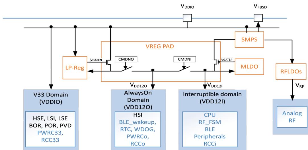
An embedded SMPS step-down converter is available (inserted between the external power and the LDOs).
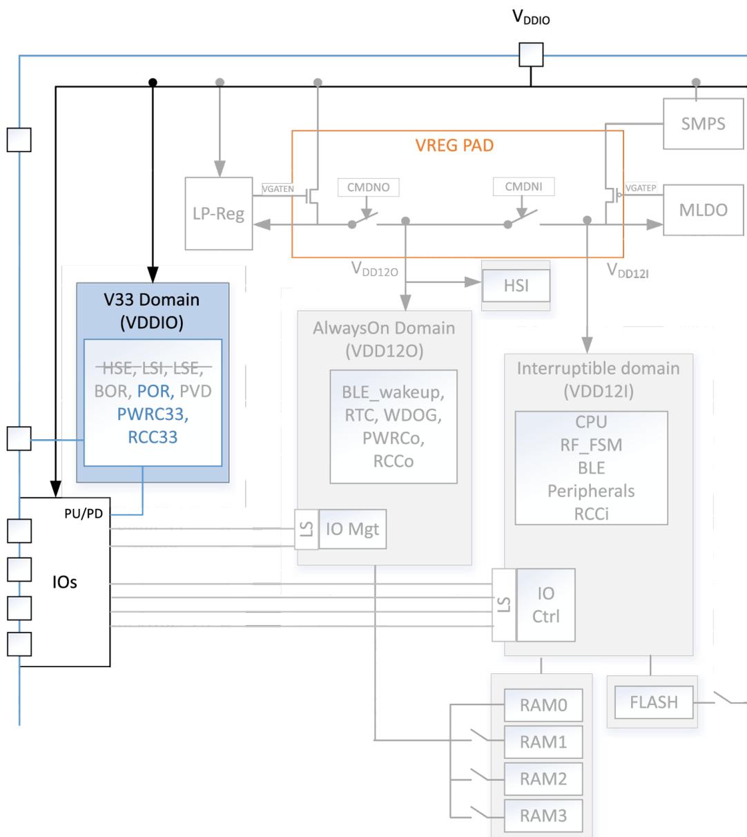
Figure 4. Power supply domain overview shows an overview of the different regulators and connections between the power supply domains.
Figure 4. Power supply domain overview
5.3 Power voltage supervisor
STM32WB07xC and STM32WB06xC devices embed several power voltage monitoring:
- • Power-on reset (POR) / power-down reset (PDR) / Brown-Out Reset (BOR)
- • Power voltage detector (PVD)
5.3.1 Power-on reset POR / power-down reset (PDR) / Brown-Out Reset (BOR)
The device has an integrated power-on reset / power-down reset, coupled with a Brown-Out Reset circuitry.
During the power-on, the device remains in reset mode as long as \( V_{DDIO} \) is below a \( V_{POR} \) threshold (typically 1.65 V).
During power-down, the PDR puts the device under reset when the supply voltage ( \( V_{DD} \) ) drops below the \( V_{PDR} \) threshold (around 20 mV below \( V_{POR} \) ). The PDR feature is always enabled.
Figure 5. Power-on reset/power-down reset waveform
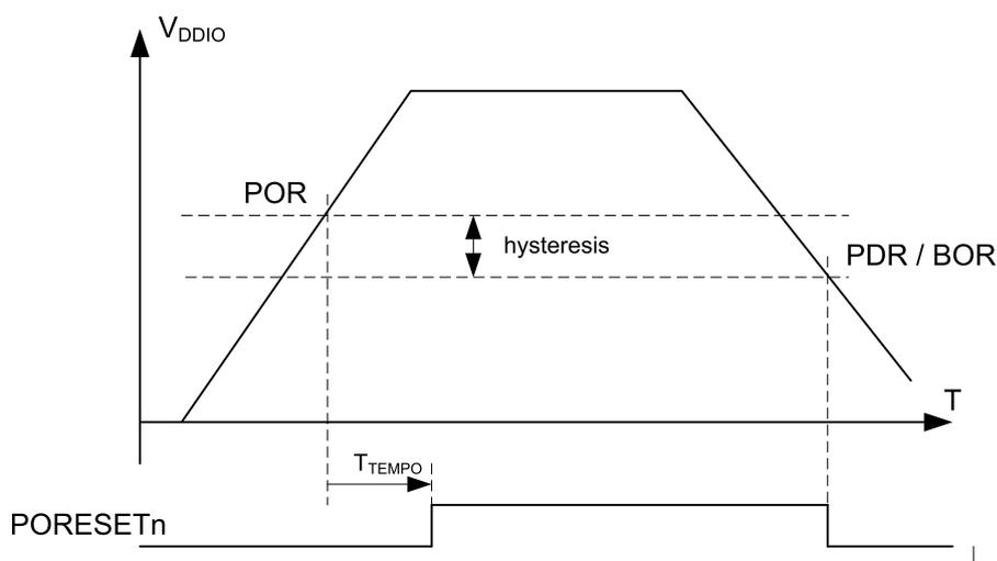
With typical values as follows:
- • \( V_{POR} \) : 1.65 V
- • Hysteresis: 20 mV (so \( V_{PDR} \) : 1.63 V)
- • \( T_{\text{TEMPO}} \) : 250 \( \mu\text{s} \)
The Brown-Out Reset (BOR) generates a device reset when the power supply (VDD) drops under \( V_{\text{PDR}} \) .
This feature is always active except during Shutdown mode where the software can decide to enable it or not (through PWRC_CR1.ENSDNBOR bit).
5.3.2 Power voltage detection (PVD)
The PVD can be used to monitor:
- • the VDDIO:
- – VDDIO is compared to a programmed threshold (between 2.05 V and 2.91 V)
- – The threshold programming is done through PWRC_CR2.PVDLS[2:0] bit field
- • an external analog input signal:
- – an external analog signal is compared to an internal VBGP (at 1.2 V) voltage
- – the feature is selected through PWRC_CR2.PVDLS[2:0] bit field
The PVD can be enabled or disabled through the PWRC_CR2.PVDE bit.
When the feature is enabled and the PVD measures a voltage below the comparator, a status flag is raised in the SYSCFG block that can generate an interrupt to the CPU if unmasked (see Section 8.2.10: Power controller interrupt status and clear register (PWRC_ISCR) ).
5.4 Operating modes
The STM32WB07xC and STM32WB06xC support three main operating modes:
- • Run mode
- • Deepstop mode
- • Shutdown mode
The transition from one mode to another is managed through a PMU state machine.
5.4.1 Run mode
In Run mode:
- • both regulators (MLDO and LPREG) are enabled
- • MLDO provides the power supply for both VDD12i and VDD12o
- • System clock and bus clock are running
- • the CPU and the radio can be used
The power consumption may be reduced by gating the clock of the unused peripherals through the RCC clock enable registers (see Section 6.6.18: RCC register map ).
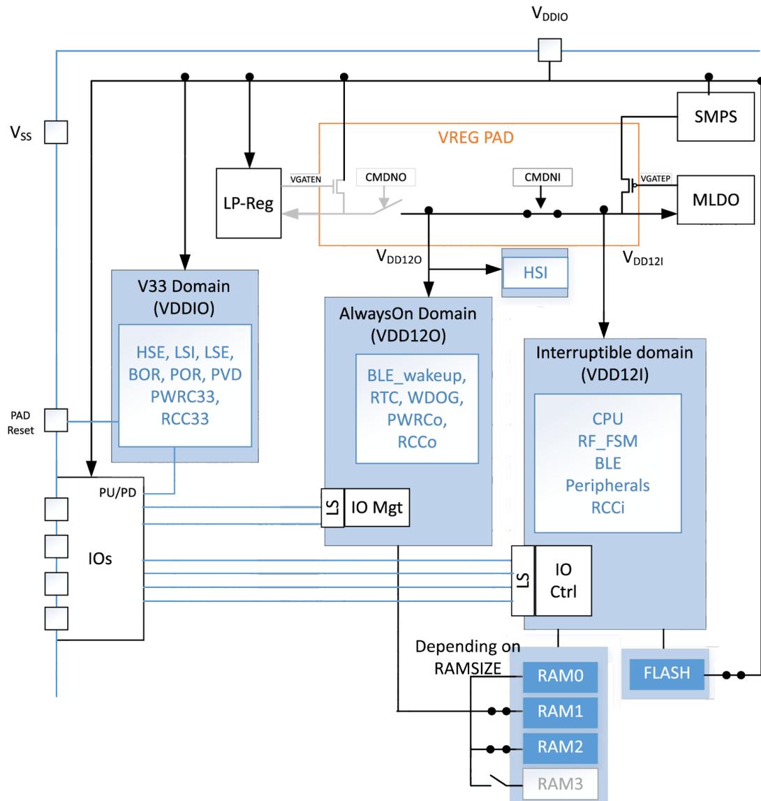
Figure 6. Power regulators and SMPS configuration in Run mode shows the regulators and SMPS configuration in Run mode with a product with only 48 Kbytes of RAM.
Figure 6. Power regulators and SMPS configuration in Run mode
5.4.2 Deepstop mode
The Deepstop is the only low-power mode of the STM32WB07xC and STM32WB06xC in order to restart from a saved context environment and go on running the application at wakeup.
The conditions to enter Deepstop mode are:
- • Radio (MR_BLE) is sleeping
- • CPU is sleeping (WFI with SLEEPDEEP information active)
- • No unmasked wakeup sources are active (including those from a previous wakeup sequence for which the software did not clear the associated flag after wakeup)
- • System is clocked on RC64MPLL (HSI or pll locked mode)
- • PWRC_CR1.LPMS bit is equal to 0
Note: If the MR_BLE is not used at all by the SoC (or not yet started), the following steps need to be done after any reset to allow low-power modes (Deepstop and Shutdown):
- • Enable the MR_BLE clock by setting the RCC_APB2ENR.MRBLEEN bit
- • Set the BLUE_SLEEP_REQUEST_MODE.FORCE_SLEEPING bit inside the wakeup block of the MR_BLE to have the MR_BLE IP requesting low-power mode to the SoC
- • Gate again the MR_BLE clock by clearing the RCC_APB2ENR.MRBLEEN bit
In Deepstop mode:
- • the system and bus clocks are stopped as the RC64MPLL block is OFF
- • the VDD12i power domain is switched off
- • the VDD12o power domain is ON and supplied at 1.0 V
- • the RAM0 bank is kept in retention
- • if PWRC_CR1.APC = 1, the I/Os pull-up/down are controlled by the PWRC_PUCRx/PWRC_PDCRx during Deepstop mode
- • the other RAM banks are in retention or not, depending on software choice in PWRC_CR2 register
- • the slow clock can be running or stopped, depending on the software configuration present before Deepstop entry:
- – ON or OFF
- – LSE or LSI source
- • RTC and the IWDG stay active (if enabled and one slow clock source is ON)
- • MR_BLE wakeup block including its timer stay active (if enabled and one slow clock source is ON)
- • eight I/Os (PA4/PA5/PA6/PA7/PA8/PA9/PA10/PA11) are able to be in output driving either a static low or high level, the slow clock information or the RTC_OUT (see Section 5.7.15: I/O Deepstop drive configuration register (PWRC_IOxCFG) for details).
A version of Deepstop mode called Deepstop2 is implemented to emulate Deepstop mode without losing the debugger connection and breakpoints or watchpoints.
- • This variant can be selected by setting the PWRC_DBGR.DEEPSTOP2 bit
- • In this case, the Deepstop mode sequence (entry and exit) is done without shutting down the VDD12i power domain
Possible wakeup sources:
- • the MR_BLE block is able to generate two events to wake up the system through its embedded wakeup timer running on slow clock:
- – BLE IP wakeup time is reached
- • the RTC is able to generate a wakeup event
- • the IWDG is able to generate a reset event
- • up to 28 GPIOs are able to wake up the system (PA0 to PA15 and PB0 to PB11)
At wakeup, the hardware resources located in the VDD12i power domain are reset, the CPU reboots. The wakeup reason is visible in a PWRC register (see Section 5.7.5: Status register 1 (PWRC_SR1) for details).
Figure 7. Power regulators and SMPS configuration in Deepstop mode shows the regulators and SMPS configuration in Deepstop mode, with a configuration requesting retention only on RAM0 and RAM1 banks.
Figure 7. Power regulators and SMPS configuration in Deepstop mode
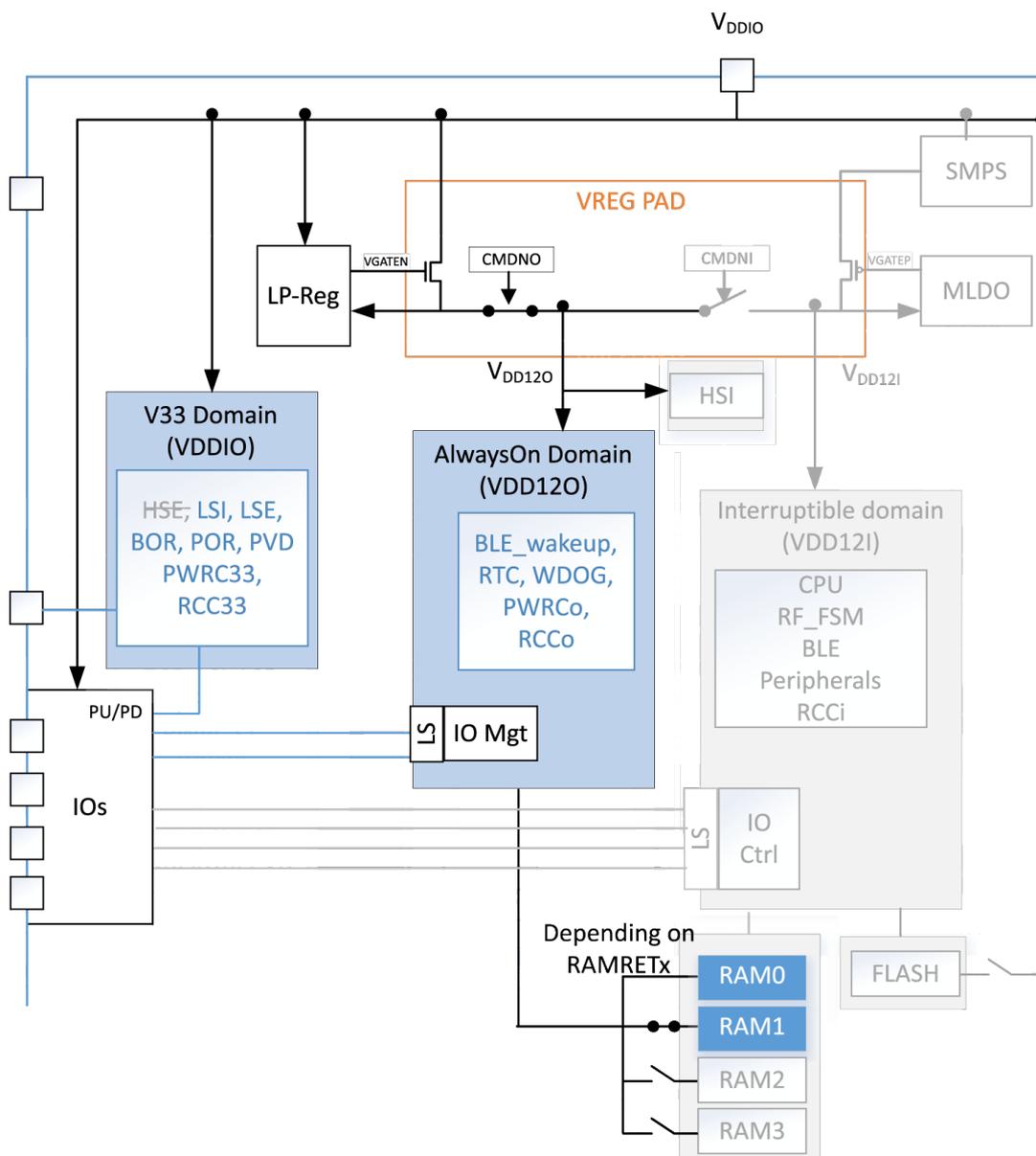
Note: Strikethrough text indicates that the feature is OFF in Deepstop mode.
5.4.3 Shutdown mode
Shutdown mode is the least power consuming mode.
The conditions to enter Shutdown mode are the same conditions needed to enter Deepstop mode except that the PWRC_CR1.LPMS bit must be equal to 1 and the PWRC_DBGR.DEEPSTOP2 bit must be kept reset.
In Shutdown mode:
- • The system is powered down as both regulators are OFF (so both VDD12i and VDD12o power domains are OFF)
- • only the VDDIO power domain is ON
- • All clocks are OFF (system and slow clock tree) as RC64MPLL, LSI and LSE are OFF,
- • if PWRC_CR1.APC = 1, the I/Os pull-up/down are controlled by the PWRC_PUCRx/PWRC_PDCRx during Shutdown mode
- • the only wakeup source is a low pulse on the RSTN pad
A Shutdown exit is similar to a POR startup of the board. The associated reset reason is the PORRSTF flag (see Section 6.6.15: V33 reset status register (RCC_CSR) for reset reason flag detail).
The BOR feature may be enabled or disabled during Shutdown through the PWRC_CR1.ENSDNBOR bit.
Figure 8. Power regulators and SMPS configuration in Shutdown mode shows the regulators and SMPS configuration in Shutdown mode, configured with the BOR reset disabled.
Figure 8. Power regulators and SMPS configuration in Shutdown mode
Note: Strikethrough text indicates that the feature is OFF in Shutdown mode.
5.4.4 Operating mode transition management
The PWRC block manages the switches from an operating mode to another through a state machine.
Figure 9. PWRC state machine for operating modes transition
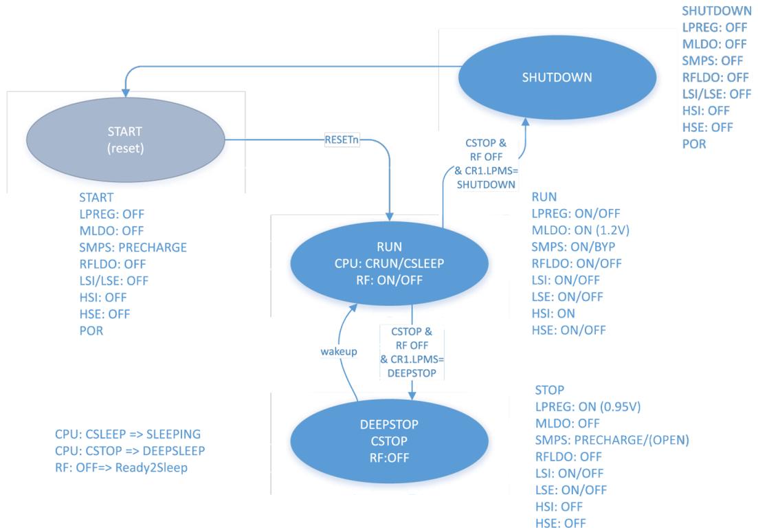
stateDiagram-v2
    [*] --> START
    START --> RUN : RESETn
    RUN --> SHUTDOWN : CSTOP & RF OFF & CR1.LPMS=SHUTDOWN
    RUN --> DEEPSTOP : CSTOP & RF OFF & CR1.LPMS=DEEPSTOP
    DEEPSTOP --> RUN : wakeup
    DEEPSTOP --> START
START (reset)
START
LPREG: OFF
MLDO: OFF
SMPS: PRECHARGE
RFLDO: OFF
LSI/LSE: OFF
HSI: OFF
HSE: OFF
POR
SHUTDOWN
SHUTDOWN
LPREG: OFF
MLDO: OFF
SMPS: OFF
RFLDO: OFF
LSI/LSE: OFF
HSI: OFF
HSE: OFF
POR
RUN
CPU: CRUN/CSLEEP
RF: ON/OFF
RUN
LPREG: ON/OFF
MLDO: ON (1.2V)
SMPS: ON/BYP
RFLDO: ON/OFF
LSI: ON/OFF
LSE: ON/OFF
HSI: ON
HSE: ON/OFF
DEEPSTOP
CPU: CSLEEP => SLEEPING
CPU: CSTOP => DEEPSLEEP
RF: OFF => Ready2Sleep
DEEPSTOP
CSTOP
RF: OFF
STOP
LPREG: ON (0.95V)
MLDO: OFF
SMPS: PRECHARGE/(OPEN)
RFLDO: OFF
LSI: ON/OFF
LSE: ON/OFF
HSI: OFF
HSE: OFF
5.5 SMPS step-down regulator
The STM32WB07xC and STM32WB06xC SMPS is a 20 mA output step-down SMPS (switch mode power supply) converter.
The SMPS output voltage can be programmed from 1.2 V to 1.90 V. It is internally clocked at 4 MHz or 8 MHz.
The SMPS can be in different configurations:
- • ON:
- – the VFBSD pin of the SMPS outputs a regulated voltage (from 1.2 V to 1.9 V)
- – the SMPS needs a clock
- • OFF:
- – the VFBSD pin has to be forced externally with VDDIO
- – the SMPS does not need a clock
- • PRECHARGE (aka BYPASS):
- – the VFBSD pin outputs the VDDIO without regulation
- – the SMPS does not need a clock
- • OPEN:
- – the VFBSD pin is floating
- – the SMPS does not need a clock
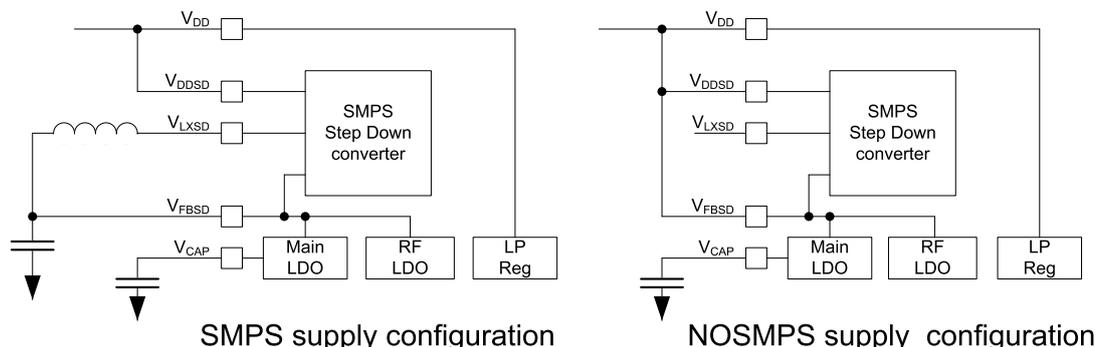
Except for the configuration SMPS OFF, an L/C BOM must be present on the board and connected to the VFBSD pad (see Figure 10. Power supply configuration).
Figure 10. Power supply configuration
The user must configure the PWRC_CR5.SMPSBOMSEL[1:0] according to the BOM implemented on their board. The value to program is indicated in Table 10. SMPS BOM information .
Table 10. SMPS BOM information
| BOM | Inductance (L) | Output capacitance (C) | SMPS BOMSEL[1:0] |
|---|---|---|---|
| BOM1 | 1.5 µH | 2.2 µF | 00 |
| BOM2 | 2.2 µH | 4.7 µF | 01 |
| BOM3 | 10 µH | 4.7 µF | 10 |
The SMPS is managed by the PWRC through a state machine shown in Figure 11. PWRC SMPS state machine overview .
Figure 11. PWRC SMPS state machine overview
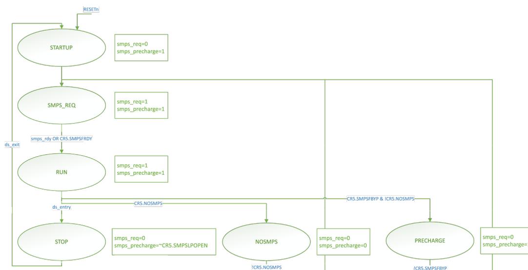
After a power-on reset sequence, the SMPS FSM always goes up to Run state. From there, the SMPS FSM can stay in three states (others are transition states):
- • Run:
- – the SMPS is ON in a Run mode
- – the SMPS clock is running
- – the VFBSD is regulated and voltage amplitude is the one programmed in the PWRC_CR5.SMPSLVL bit field
- – the L/C BOM is present on the board and is connected on the VFBSD pad of the STM32WB07xC and STM32WB06xC (see Figure 10. Power supply configuration )
- • NO SMPS (if the software configures PWRC_CR5.NOSMPS=1):
- – the SMPS is OFF
- – the SMPS clock is stopped
- – the VFBSD is directly connected to the VDDIO through the VFBSD pad of the STM32WB07xC and STM32WB06xC (see Figure 10. Power supply configuration )
- – the PWRC does not control any specific sequencing on the SMPS during low-power entry/exit phases
- • PRECHARGE aka BYPASS (if the software configures PWRC_CR5.SMPSFBYP=1):
- – the SMPS is ON in a precharge mode
- – the SMPS clock is stopped
- – the VFBSD is the VDDIO voltage crossing the SMPS block
- – the PWRC does not control any specific sequencing on the SMPS during low-power entry/exit phases
- – this mode is compliant with an L/C BOM connected on the VFBSD pad of the STM32WB07xC and STM32WB06xC
When the device enters Deepstop mode, the PWRC automatically switches the SMPS from Run to Deepstop mode which can be:
- – if PWRC_CR5.SMPSLPOPEN = 0: SMPS output is the VDDIO (as in PRECHARGE FSM state)
- – if PWRC_CR5.SMPSLPOPEN = 1: the SMPS output is floating
5.6 I/O pull-ups/pull-downs during low power mode
When PWRC_CR1.APC is set (default configuration), the pull-up/pull-down of the IOs is controlled by the PWRC_PUCRx and PWRC_PDCRx registers of the PWRC block, instead of GPIOx_PUPDR register of the GPIO block. This feature avoids glitches on the lines by keeping the same pull-up/pull-down configuration during all the supported operating modes.
5.7 PWRC registers
All PWRC APB registers are only 16-bit registers. The 16 MSB bits are always stuck to 0.
5.7.1 Control register 1 (PWRC_CR1)
This register controls the BOR in Shutdown, the low-power mode selection and the IO control owner.
Address offset: 0x00
Reset value: 0x0000 0010
| 31 | 30 | 29 | 28 | 27 | 26 | 25 | 24 | 23 | 22 | 21 | 20 | 19 | 18 | 17 | 16 |
|---|---|---|---|---|---|---|---|---|---|---|---|---|---|---|---|
| Res. | Res. | Res. | Res. | Res. | Res. | Res. | Res. | Res. | Res. | Res. | Res. | Res. | Res. | Res. | Res. |
| 15 | 14 | 13 | 12 | 11 | 10 | 9 | 8 | 7 | 6 | 5 | 4 | 3 | 2 | 1 | 0 |
| Res. | Res. | Res. | Res. | Res. | Res. | Res. | Res. | Res. | Res. | Res. | APC rw | Res. | Res. | ENSDNBOR rw | LPMS rw |
| Bits 31:5 | Reserved, must be kept at reset value. |
| Bit 4 | APC:
Apply pull-up/down configuration from PWRC or GPIO register.
|
| Bits 3:2 | Reserved, must be kept at reset value. |
| Bit 1 | ENSDNBOR:
Enable BOR reset supervising during Shutdown mode.
|
| Bit 0 | LPMS:
Low-power mode selection. This bit defines whether the device enters Deepstop or Shutdown mode when both CPU and MR_BLE requests a low-power mode entry.
|
5.7.2 Control register 2 (PWRC_CR2)
Address offset: 0x04
Reset value: 0x0000 0100
| 31 | 30 | 29 | 28 | 27 | 26 | 25 | 24 | 23 | 22 | 21 | 20 | 19 | 18 | 17 | 16 |
|---|---|---|---|---|---|---|---|---|---|---|---|---|---|---|---|
| Res. | Res. | Res. | Res. | Res. | Res. | Res. | Res. | Res. | Res. | Res. | Res. | Res. | Res. | Res. | Res. |
| 15 | 14 | 13 | 12 | 11 | 10 | 9 | 8 | 7 | 6 | 5 | 4 | 3 | 2 | 1 | 0 |
| Res. | Res. | Res. | Res. | Res. | LSILPMUFEN | ENTS | Res. | RAMRET3 | RAMRET2 | RAMRET1 | Res. | PVDLS[2:0] | PVDE | ||
| rw | rw | rw | rw | rw | rw | rw | rw | rw | |||||||
| Bits 31:11 | Reserved, must be kept at reset value. |
| Bit 10 | LSILPMUFEN:
LSI LPMU force enable.
|
| Bit 9 | ENTS:
Enable the temperature sensor.
|
| Bit 8 | Reserved, must be kept at reset value. |
| Bit 7 | RAMRET3:
Enables the RAM3 bank retention in Deepstop mode.
|
| Bit 6 | RAMRET2:
Enables the RAM2 bank retention in Deepstop mode.
|
| Bit 5 | RAMRET1:
Enables the RAM1 bank retention in Deepstop mode.
|
| Bit 4 | Reserved, must be kept at reset value. |
| Bits 3:1 | PVDLS[2:0]:
Programmable voltage detector level selection:
|
| Bit 0 | PVDE:
Programmable voltage detector enable.
|
5.7.3 Control register 3 (PWRC_CR3)
This register manages the selection of the wakeup sources to get out of Deepstop mode.
Note: All wakeup sources are disabled by default after reset.
Address offset: 0x08
Reset value: 0x0000 0000
| 31 | 30 | 29 | 28 | 27 | 26 | 25 | 24 | 23 | 22 | 21 | 20 | 19 | 18 | 17 | 16 |
|---|---|---|---|---|---|---|---|---|---|---|---|---|---|---|---|
| Res. | Res. | Res. | Res. | Res. | Res. | Res. | Res. | Res. | Res. | Res. | Res. | Res. | Res. | Res. | Res. |
| 15 | 14 | 13 | 12 | 11 | 10 | 9 | 8 | 7 | 6 | 5 | 4 | 3 | 2 | 1 | 0 |
| EIWL | Res. | EWBLE HCPU | EWBLE | EWU11 | EWU10 | EWU9 | EWU8 | EWU7 | EWU6 | EWU5 | EWU4 | EWU3 | EWU2 | EWU1 | EWU0 |
| rw | rw | rw | rw | rw | rw | rw | rw | rw | rw | rw | rw | rw | rw | rw |
| Bits 31:16 | Reserved, must be kept at reset value. |
| Bit 15 | EIWL:
Enable wakeup on internal event (RTC).
|
| Bit 14 | Reserved, must be kept at reset value. |
| Bit 13 | EWBLEHCPU:
Enable wakeup on BLE Host CPU event.
|
| Bit 12 | EWBLE:
Enable wakeup on BLE event.
|
| Bit 11 | EWU11:
Enable wakeup on PA11 I/O event.
|
| Bit 10 | EWU10:
Enable wakeup on PA10 I/O event.
|
| Bit 9 | EWU9:
Enable wakeup on PA9 I/O event.
|
| Bit 8 | EWU8:
Enable wakeup on PA8 I/O event.
|
| Bit 7 | EWU7:
Enable wakeup on PB7 I/O event.
|
| Bit 6 | EWU6:
Enable wakeup on PB6 I/O event.
|
| Bit 5 | EWU5:
Enable wakeup on PB5 I/O event.
|
| Bit 4 | EWU4:
Enable wakeup on PB4 I/O event.
|
| Bit 3 | EWU3:
Enable wakeup on PB3 I/O event.
|
| Bit 2 | EWU2:
Enable wakeup on PB2 I/O event.
|
| Bit 1 | EWU1:
Enable wakeup on PB1 I/O event.
|
| Bit 0 | EWU0:
Enable wakeup on PB0 I/O event.
|
5.7.4 Control register 4 (PWRC_CR4)
This register manages the polarity for the I/Os wakeup sources to get out of Deepstop mode.
Note: The wakeup events are edge detection only, not level detection.
Address offset: 0x0C
Reset value: 0x0000 0000
| 31 | 30 | 29 | 28 | 27 | 26 | 25 | 24 | 23 | 22 | 21 | 20 | 19 | 18 | 17 | 16 |
| Res. | Res. | Res. | Res. | Res. | Res. | Res. | Res. | Res. | Res. | Res. | Res. | Res. | Res. | Res. | Res. |
| 15 | 14 | 13 | 12 | 11 | 10 | 9 | 8 | 7 | 6 | 5 | 4 | 3 | 2 | 1 | 0 |
| Res. | Res. | Res. | Res. | WUP11 | WUP10 | WUP9 | WUP8 | WUP7 | WUP6 | WUP5 | WUP4 | WUP3 | WUP2 | WUP1 | WUP0 |
| rw | rw | rw | rw | rw | rw | rw | rw | rw | rw | rw | rw |
| Bits 31:12 | Reserved, must be kept at reset value. |
| Bit 11 | WUP11:
Wakeup polarity for PA11 I/O.
|
| Bit 10 | WUP10:
Wakeup polarity for PA10 I/O.
|
| Bit 9 | WUP9:
Wakeup polarity for PA9 IO event.
|
| Bit 8 | WUP8:
Wakeup polarity for PA8 IO event.
|
| Bit 7 | WUP7:
Wakeup polarity for PB7 IO event.
|
| Bit 6 | WUP6:
Wakeup polarity for PB6 IO event.
|
| Bit 5 | WUP5:
Wakeup polarity for PB5 IO event.
|
| Bit 4 | WUP4:
Wakeup polarity for PB4 IO event.
|
| Bit 3 | WUP3:
Wakeup polarity for PB3 IO event.
|
| Bit 2 | WUP2:
Wakeup polarity for PB2 IO event.
|
| Bit 1 | WUP1:
Wakeup polarity for PB1 IO event.
|
| Bit 0 | WUP0:
Wakeup polarity for PB0 IO event.
|
| Bit 2 | WUP2:
Wakeup polarity for PB2 IO event.
|
| Bit 1 | WUP1:
Wakeup polarity for PB1 IO event.
|
| Bit 0 | WUP0:
Wakeup polarity for PB0 IO event.
|
5.7.5 Status register 1 (PWRC_SR1)
This register provides the information concerning which source woke up the device after a Deepstop.
Address offset: 0x10
Reset value: 0x0000 0000
| 31 | 30 | 29 | 28 | 27 | 26 | 25 | 24 | 23 | 22 | 21 | 20 | 19 | 18 | 17 | 16 |
| Res. | Res. | Res. | Res. | Res. | Res. | Res. | Res. | Res. | Res. | Res. | Res. | Res. | Res. | Res. | Res. |
| 15 | 14 | 13 | 12 | 11 | 10 | 9 | 8 | 7 | 6 | 5 | 4 | 3 | 2 | 1 | 0 |
| IWUF | Res. | WBLE HCPUF | WBLEF | WUF11 | WUF10 | WUF9 | WUF8 | WUF7 | WUF6 | WUF5 | WUF4 | WUF3 | WUF2 | WUF1 | WUF0 |
| r | rc_w1 | rc_w1 | rc_w1 | rc_w1 | rc_w1 | rc_w1 | rc_w1 | rc_w1 | rc_w1 | rc_w1 | rc_w1 | rc_w1 | rc_w1 | rc_w1 |
| Bits 31:16 | Reserved, must be kept at reset value. |
| Bit 15 | IWUF:
Internal wakeup flag (RTC).
|
| Bit 14 | Reserved, must be kept at reset value. |
| Bit 13 | WBLEHCPUF:
BLE Host CPU wakeup flag.
|
| Bit 12 | WBLEF:
BLE wakeup flag.
|
| Bit 11 | WUF11:
PA11 I/O wakeup flag.
|
| Bit 10 | WUF10:
PA10 I/O wakeup flag.
|
| Bit 9 | WUF9:
PA9 I/O wakeup flag.
|
| Bit 8 | WUF8:
PA8 I/O wakeup flag.
|
| Bit 7 | WUF7:
PB7 I/O wakeup flag.
|
| Bit 6 | WUF6:
PB6 I/O wakeup flag.
|
| Bit 5 | WUF5:
PB5 I/O wakeup flag.
|
| Bit 4 | WUF4:
PB4 I/O wakeup flag.
|
| Bit 3 | WUF3:
PB3 I/O wakeup flag.
|
| Bit 2 | WUF2:
PB2 I/O wakeup flag.
|
| Bit 1 | WUF1:
PB1 I/O wakeup flag.
|
| Bit 0 | WUF0:
PB0 I/O wakeup flag.
|
5.7.6 Status register 2 (PWRC_SR2)
This register provides some status flags related to the power voltage detector and the SMPS blocks.
Address offset: 0x14
Reset value: 0x0000 -306
| 31 | 30 | 29 | 28 | 27 | 26 | 25 | 24 | 23 | 22 | 21 | 20 | 19 | 18 | 17 | 16 |
|---|---|---|---|---|---|---|---|---|---|---|---|---|---|---|---|
| Res. | Res. | Res. | Res. | Res. | Res. | Res. | Res. | Res. | Res. | Res. | Res. | Res. | Res. | Res. | Res. |
| 15 | 14 | 13 | 12 | 11 | 10 | 9 | 8 | 7 | 6 | 5 | 4 | 3 | 2 | 1 | 0 |
| IOBOOTVAL[3:0] | PVDO | Res. | REGMS | REGLPS | Res. | Res. | Res. | Res. | Res. | SMPS RDY | SMPSE NR | SMPSB YPR | |||
| r | r | r | r | r | r | r | r | r | r | ||||||
| Bits 31:16 | Reserved, must be kept at reset value. |
| Bits 15:12 | IOBOOTVAL:
I/Os value latched at POR.
|
| Bit 11 | PVDO:
Power voltage Detector Output. When the Power voltage Detector is enabled (PWRC_CR2.PVDE=1), this bit indicates when the VDDIO is lower than the selected threshold (through PWRC_CR2.PVDLS bit field).
|
| Bit 10 | Reserved, must be kept at reset value. |
| Bit 9 | REGMS:
Main regulator ready status.
|
| Bit 8 | REGLPS:
Low-power regulator ready status.
|
| Bits 7:3 | Reserved, must be kept at reset value. |
| Bit 2 | SMPSRDY:
SMPS ready status.
|
| Bit 1 | SMPSENR:
SMPS Run mode status. This bit mirrors the internal ENABLE_3V3 control signal connected to the SMPS and driven by the hardware.
|
| Bit 0 | SMPSBYPR:
SMPS PRECHARGE mode status. This bit mirrors the PRECHARGE control state of the SMPS.
|
5.7.7 Control register 5 (PWRC_CR5)
This register is used to configure the SMPS.
Address offset: 0x1C
Reset value: 0x0000 0014
| 31 | 30 | 29 | 28 | 27 | 26 | 25 | 24 | 23 | 22 | 21 | 20 | 19 | 18 | 17 | 16 |
|---|---|---|---|---|---|---|---|---|---|---|---|---|---|---|---|
| Res. | Res. | Res. | Res. | Res. | Res. | Res. | Res. | Res. | Res. | Res. | Res. | Res. | Res. | Res. | Res. |
| 15 | 14 | 13 | 12 | 11 | 10 | 9 | 8 | 7 | 6 | 5 | 4 | 3 | 2 | 1 | 0 |
| Res. | Res. | Res. | CLKDE TR_DI SABLE | SMPS_ENA_D CM | NOSM PS | SMPSF BYP | SMPSL POPEN | Res. | Res. | SMPSBOMSEL[ 1:0] | SMP SLVL[3:0] | ||||
| rw | rw | rw | rw | rw | rw | rw | rw | rw | rw | rw | |||||
| Bits 31:13 | Reserved, must be kept at reset value. |
| Bit 12 | CLKDETR_DISABLE: Disables the SMPS clock detection. The SMPS clock detection enables an automatic SMPS bypass switching in case of unexpected loss of the SMPS clock.
|
| Bit 11 | SMPS_ENA_DCM: Discontinuous conduction mode enable.
|
| Bit 10 | NOSMPS: No SMPS mode.
Note: This configuration (SMPS disabled) should be used only when the SMPS_FB pad is directly connected to the VBATT (external voltage), without L/C BOM. |
| Bit 9 | SMPSFBYP: Forces the SMPS in PRECHARGE mode.
Note: When this bit is set, the VSMP S output is connected to the VDDIO. The actual state of the SMPS is visible in the SMPS mode status bits in PWRC_SR2 register. |
| Bit 8 | SMPSLPOPEN: Select OPEN mode instead of PRECHARGE mode for the SMPS during Deepstop.
|
| Bits 7:6 | Reserved, must be kept at reset value. |
| Bits 5:4 | SMPSBOMSEL[1:0]: Select the SMPS BOM.
Note: BOM correspondence/details is available in Table 10. SMPS BOM information. |
| Bits 3:0 | SMPSLVL[3:0] : Select the SMPS output voltage level. This bit field selects the SMPS voltage output level with a granularity of 50 mV. The SMPS output voltage level, V SMPS , must be configured such that \( V_{BAT} - V_{SMPS} \geq 0.2 \) V. [e.g. For \( V_{BAT}=2 \) V, V SMPS must be no higher than 1.8 V]
Warning: The SMPS output voltage must not be changed by more than one step while the SMPS is in use. The sequence to reprogram a new SMPS output voltage is described in Section 5.8.2: SMPS output level re-programming . |
5.7.8 I/O port A pull-up control register (PWRC_PUCRA)
This register is used to control the pull-up for the PA0 to PA15 I/O when the PWRC_CR1.APC bit is set.
Caution: If both pull-up and pull-down are enabled in the PWRC_PUCRA and PWRC_PDCRA registers for an I/O, then pull-down is applied.
The user must take care to disable the pull-on I/O programmed in analog mode.
Address offset: 0x20
Reset value: 0x0000 FFF7
| 31 | 30 | 29 | 28 | 27 | 26 | 25 | 24 | 23 | 22 | 21 | 20 | 19 | 18 | 17 | 16 |
| Res. | Res. | Res. | Res. | Res. | Res. | Res. | Res. | Res. | Res. | Res. | Res. | Res. | Res. | Res. | Res. |
| 15 | 14 | 13 | 12 | 11 | 10 | 9 | 8 | 7 | 6 | 5 | 4 | 3 | 2 | 1 | 0 |
| PUA15 | PUA14 | PUA13 | PUA12 | PUA11 | PUA10 | PUA9 | PUA8 | PUA7 | PUA6 | PUA5 | PUA4 | PUA3 | PUA2 | PUA1 | PUA0 |
| rw | rw | rw | rw | rw | rw | rw | rw | rw | rw | rw | rw | rw | rw | rw | rw |
| Bits 31:16 | Reserved, must be kept at reset value. |
| Bit 15 | PUA15:
Pull-up enable for PA15 I/O.
|
| Bit 14 | PUA14:
Pull-up enable for PA14 I/O.
|
| Bit 13 | PUA13:
Pull-up enable for PA13 I/O.
|
| Bit 12 | PUA12:
Pull-up enable for PA12 I/O.
|
| Bit 11 | PUA11:
Pull-up enable for PA11 I/O.
|
| Bit 10 | PUA10:
Pull-up enable for PA10 I/O.
|
| Bit 9 | PUA9:
Pull-up enable for PA9 I/O.
|
| Bit 8 | PUA8:
Pull-up enable for PA8 I/O.
|
| Bit 7 | PUA7:
Pull-up enable for PA7 I/O.
|
| Bit 6 | PUA6:
Pull-up enable for PA6 I/O.
|
| Bit 5 | PUA5:
Pull-up enable for PA5 I/O.
|
| Bit 4 | PUA4:
Pull-up enable for PA4 I/O.
|
| Bit 3 | PUA3:
Pull-up enable for PA3 I/O.
|
| Bit 2 | PUA2:
Pull-up enable for PA2 I/O.
|
| Bit 1 | PUA1:
Pull-up enable for PA1 I/O.
|
| Bit 0 | PUA0:
Pull-up enable for PA0 I/O.
|
5.7.9 I/O port A pull-down control register (PWRC_PDCRA)
This register is used to control the pull-down for the PA0 to PA15 I/O when the PWRC_CR1.APC bit is set.
Caution: If both pull-up and pull-down are enabled in the PWRC_PUCRA and PWRC_PDCRA registers for an I/O, then pull-down is applied.
The user must take care to disable the pull-on I/O programmed in analog mode.
Address offset: 0x24
Reset value: 0x0000 0008
| 31 | 30 | 29 | 28 | 27 | 26 | 25 | 24 | 23 | 22 | 21 | 20 | 19 | 18 | 17 | 16 |
| Res. | Res. | Res. | Res. | Res. | Res. | Res. | Res. | Res. | Res. | Res. | Res. | Res. | Res. | Res. | Res. |
| 15 | 14 | 13 | 12 | 11 | 10 | 9 | 8 | 7 | 6 | 5 | 4 | 3 | 2 | 1 | 0 |
| PDA15 | PDA14 | PDA13 | PDA12 | PDA11 | PDA10 | PDA9 | PDA8 | PDA7 | PDA6 | PDA5 | PDA4 | PDA3 | PDA2 | PDA1 | PDA0 |
| rw | rw | rw | rw | rw | rw | rw | rw | rw | rw | rw | rw | rw | rw | rw | rw |
| Bits 31:16 | Reserved, must be kept at reset value. |
| Bit 15 | PDA15:
Pull-down enable for PA15 I/O.
|
| Bit 14 | PDA14:
Pull-down enable for PA14 I/O.
|
| Bit 13 | PDA13:
Pull-down enable for PA13 I/O.
|
| Bit 12 | PDA12:
Pull-down enable for PA12 I/O.
|
| Bit 11 | PDA11:
Pull-down enable for PA11 I/O.
|
| Bit 10 | PDA10:
Pull-down enable for PA10 I/O.
|
| Bit 9 | PDA9:
Pull-down enable for PA9 I/O.
|
| Bit 8 | PDA8:
Pull-down enable for PA8 I/O.
|
| Bit 7 | PDA7:
Pull-down enable for PA7 I/O.
|
| Bit 6 | PDA6:
Pull-down enable for PA6 I/O.
|
| Bit 5 | PDA5:
Pull-down enable for PA5 I/O.
|
| Bit 4 | PDA4:
Pull-down enable for PA4 I/O.
|
| Bit 3 | PDA3:
Pull-down enable for PA3 I/O.
|
| Bit 2 | PDA2:
Pull-down enable for PA2 I/O.
|
| Bit 1 | PDA1:
Pull-down enable for PA1 I/O.
|
| Bit 0 | PDA0:
Pull-down enable for PA0 I/O.
|
5.7.10 I/O port B pull-up control register (PWRC_PUCRB)
This register is used to control the pull-up for the PB0 to PB15 I/O when the PWRC_CR1.APC bit is set.
Caution: If both pull-up and pull-down are enabled in the PWRC_PUCRA and PWRC_PDCRA registers for an I/O, then pull-down is applied.
The user must take care to disable the pull-on I/O programmed in analog mode.
Address offset: 0x28
Reset value: 0x0000 FFFF
| 31 | 30 | 29 | 28 | 27 | 26 | 25 | 24 | 23 | 22 | 21 | 20 | 19 | 18 | 17 | 16 |
|---|---|---|---|---|---|---|---|---|---|---|---|---|---|---|---|
| Res. | Res. | Res. | Res. | Res. | Res. | Res. | Res. | Res. | Res. | Res. | Res. | Res. | Res. | Res. | Res. |
| 15 | 14 | 13 | 12 | 11 | 10 | 9 | 8 | 7 | 6 | 5 | 4 | 3 | 2 | 1 | 0 |
| PUB15 | PUB14 | PUB13 | PUB12 | PUB11 | PUB10 | PUB9 | PUB8 | PUB7 | PUB6 | PUB5 | PUB4 | PUB3 | PUB2 | PUB1 | PUB0 |
| rw | rw | rw | rw | rw | rw | rw | rw | rw | rw | rw | rw | rw | rw | rw | rw |
| Bits 31:16 | Reserved, must be kept at reset value. |
| Bit 15 | PUB15:
Pull-up enable for PB15 I/O.
|
| Bit 14 | PUB14:
Pull-up enable for PB14 I/O.
|
| Bit 13 | PUB13:
Pull-up enable for PB13 I/O.
|
| Bit 12 | PUB12:
Pull-up enable for PB12 I/O.
|
| Bit 11 | PUB11:
Pull-up enable for PB11 I/O.
|
| Bit 10 | PUB10:
Pull-up enable for PB10 I/O.
|
| Bit 9 | PUB9:
Pull-up enable for PB9 I/O.
|
| Bit 8 | PUB8:
Pull-up enable for PB8 I/O.
|
| Bit 7 | PUB7:
Pull-up enable for PB7 I/O.
|
| Bit 6 | PUB6:
Pull-up enable for PB6 I/O.
|
| Bit 5 | PUB5:
Pull-up enable for PB5 I/O.
|
| Bit 4 | PUB4:
Pull-up enable for PB4 I/O.
|
| Bit 3 | PUB3:
Pull-up enable for PB3 I/O.
|
| Bit 2 | PUB2:
Pull-up enable for PB2 I/O.
|
| Bit 1 | PUB1:
Pull-up enable for PB1 I/O.
|
| Bit 0 | PUB0:
Pull-up enable for PB0 I/O.
|
5.7.11 I/O port B pull-down control register (PWRC_PDCRB)
This register is used to control the pull-down for the PB0 to PB15 I/O when the PWRC_CR1.APC bit is set.
Caution: If both pull-up and pull-down are enabled in the PWRC_PUCRA and PWRC_PDCRA registers for an I/O, then pull-down is applied.
The user must take care to disable the pull-up I/O programmed in Analog mode.
Address offset: 0x2C
Reset value: 0x0000 0000
| 31 | 30 | 29 | 28 | 27 | 26 | 25 | 24 | 23 | 22 | 21 | 20 | 19 | 18 | 17 | 16 |
| Res. | Res. | Res. | Res. | Res. | Res. | Res. | Res. | Res. | Res. | Res. | Res. | Res. | Res. | Res. | Res. |
| 15 | 14 | 13 | 12 | 11 | 10 | 9 | 8 | 7 | 6 | 5 | 4 | 3 | 2 | 1 | 0 |
| PDB15 | PDB14 | PDB13 | PDB12 | PDB11 | PDB10 | PDB9 | PDB8 | PDB7 | PDB6 | PDB5 | PDB4 | PDB3 | PDB2 | PDB1 | PDB0 |
| rw | rw | rw | rw | rw | rw | rw | rw | rw | rw | rw | rw | rw | rw | rw | rw |
| Bits 31:16 | Reserved, must be kept at reset value. |
| Bit 15 | PDB15:
Pull-down enable for PB15 I/O.
|
| Bit 14 | PDB14:
Pull-down enable for PB14 I/O.
|
| Bit 13 | PDB13:
Pull-down enable for PB13 I/O.
|
| Bit 12 | PDB12:
Pull-down enable for PB12 I/O.
|
| Bit 11 | PDB11:
Pull-down enable for PB11 I/O.
|
| Bit 10 | PDB10:
Pull-down enable for PB10 I/O.
|
| Bit 9 | PDB9:
Pull-down enable for PB9 I/O.
|
| Bit 8 | PDB8:
Pull-down enable for PB8 I/O.
|
| Bit 7 | PDB7:
Pull-down enable for PB7 I/O.
|
| Bit 6 | PDB6:
Pull-down enable for PB6 I/O.
|
| Bit 5 | PDB5:
Pull-down enable for PB5 I/O.
|
| Bit 4 | PDB4:
Pull-down enable for PB4 I/O.
|
| Bit 3 | PDB3:
Pull-down enable for PB3 I/O.
|
| Bit 2 | PDB2:
Pull-down enable for PB2 I/O.
|
| Bit 1 | PDB1:
Pull-down enable for PB1 I/O.
|
| Bit 0 | PDB0:
Pull-down enable for PB0 I/O.
|
5.7.12 Control register 6 (PWRC_CR6)
This register manages the selection of the wakeup sources to get out of Deepstop mode.
Note: All wakeup sources are disabled by default after reset.
Address offset: 0x30
Reset value: 0x0000 0000
| 31 | 30 | 29 | 28 | 27 | 26 | 25 | 24 | 23 | 22 | 21 | 20 | 19 | 18 | 17 | 16 |
| Res. | Res. | Res. | Res. | Res. | Res. | Res. | Res. | Res. | Res. | Res. | Res. | Res. | Res. | Res. | Res. |
| 15 | 14 | 13 | 12 | 11 | 10 | 9 | 8 | 7 | 6 | 5 | 4 | 3 | 2 | 1 | 0 |
| EWU27 | EWU26 | EWU25 | EWU24 | EWU22 | EWU22 | EWU21 | EWU20 | EWU19 | EWU18 | EWU17 | EWU16 | EWU15 | EWU14 | EWU13 | EWU12 |
| rw | rw | rw | rw | rw | rw | rw | rw | rw | rw | rw | rw | rw | rw | rw | rw |
| Bits 31:16 | Reserved, must be kept at reset value. |
| Bit 15 | EWU27:
Enable wakeup on PA15 I/O event.
|
| Bit 14 | EWU26:
Enable wakeup on PA14 I/O event.
|
| Bit 13 | EWU25:
Enable wakeup on PA13 I/O event.
|
| Bit 12 | EWU24:
Enable wakeup on PA12 I/O event.
|
| Bit 11 | EWU23:
Enable wakeup on PB11 I/O event.
|
| Bit 10 | EWU22:
Enable wakeup on PB10 I/O event.
|
| Bit 9 | EWU21:
Enable wakeup on PB9 I/O event.
|
| Bit 8 | EWU20:
Enable wakeup on PB8 I/O event.
|
| Bit 7 | EWU19:
Enable wakeup on PA7 I/O event.
|
| Bit 6 | EWU18:
Enable wakeup on PA6 I/O event.
|
| Bit 5 | EWU17:
Enable wakeup on PA5 I/O event.
|
| Bit 4 | EWU16:
Enable wakeup on PA4 I/O event.
|
| Bit 3 | EWU15:
Enable wakeup on PA3 I/O event.
|
| Bit 2 | EWU14:
Enable wakeup on PA2 I/O event.
|
| Bit 1 | EWU13:
Enable wakeup on PA1 I/O event.
|
| Bit 0 | EWU12:
Enable wakeup on PA0 I/O event.
|
5.7.13 Control register 7 (PWRC_CR7)
This register manages the polarity for the I/Os wakeup sources to get out of Deepstop mode.
Note: The wakeup events are only edge detection, not level detection.
Address offset: 0x34
Reset value: 0x0000 0000
| 31 | 30 | 29 | 28 | 27 | 26 | 25 | 24 | 23 | 22 | 21 | 20 | 19 | 18 | 17 | 16 |
| Res. | Res. | Res. | Res. | Res. | Res. | Res. | Res. | Res. | Res. | Res. | Res. | Res. | Res. | Res. | Res. |
| 15 | 14 | 13 | 12 | 11 | 10 | 9 | 8 | 7 | 6 | 5 | 4 | 3 | 2 | 1 | 0 |
| WUP27 | WUP26 | WUP25 | WUP24 | WUP23 | WUP22 | WUP21 | WUP20 | WUP19 | WUP18 | WUP17 | WUP16 | WUP15 | WUP14 | WUP13 | WUP12 |
| rw | rw | rw | rw | rw | rw | rw | rw | rw | rw | rw | rw | rw | rw | rw | rw |
| Bits 31:16 | Reserved, must be kept at reset value. |
| Bit 15 | WUP27:
Wakeup polarity for PA15 I/O.
|
| Bit 14 | WUP26:
Wakeup polarity for PA14 I/O.
|
| Bit 13 | WUP25:
Wakeup polarity for PA13 IO event.
|
| Bit 12 | WUP24:
Wakeup polarity for PA12 I/O.
|
| Bit 11 | WUP23:
Wakeup polarity for PB11 I/O.
|
| Bit 10 | WUP22:
Wakeup polarity for PB10 I/O.
|
| Bit 9 | WUP21:
Wakeup polarity for PB9 IO event.
|
| Bit 8 | WUP20:
Wakeup polarity for PB8 IO event.
|
| Bit 7 | WUP19:
Wakeup polarity for PA7 IO event.
|
| Bit 6 | WUP18:
Wakeup polarity for PA6 IO event.
|
| Bit 5 | WUP17:
Wakeup polarity for PA5 IO event.
|
| Bit 4 | WUP16:
Wakeup polarity for PA4 IO event.
|
| Bit 3 | WUP15:
Wakeup polarity for PA3 IO event.
|
| Bit 2 | WUP14:
Wakeup polarity for PA2 IO event.
|
| Bit 1 | WUP13:
Wakeup polarity for PA1 IO event.
|
| Bit 0 | WUP12:
Wakeup polarity for PA0 IO event.
|
5.7.14 Status register 3(PWRC_SR3)
This register provides some information about which source woke up the device after a Deepstop.
Address offset: 0x38
Reset value: 0x0000 0000
| 31 | 30 | 29 | 28 | 27 | 26 | 25 | 24 | 23 | 22 | 21 | 20 | 19 | 18 | 17 | 16 |
| Res. | Res. | Res. | Res. | Res. | Res. | Res. | Res. | Res. | Res. | Res. | Res. | Res. | Res. | Res. | Res. |
| 15 | 14 | 13 | 12 | 11 | 10 | 9 | 8 | 7 | 6 | 5 | 4 | 3 | 2 | 1 | 0 |
| WUF27 | WUF26 | WUF25 | WUF24 | WUF23 | WUF22 | WUF21 | WUF20 | WUF19 | WUF18 | WUF17 | WUF16 | WUF15 | WUF14 | WUF13 | WUF12 |
| rc_w1 | rc_w1 | rc_w1 | rc_w1 | rc_w1 | rc_w1 | rc_w1 | rc_w1 | rc_w1 | rc_w1 | rc_w1 | rc_w1 | rc_w1 | rc_w1 | rc_w1 | rc_w1 |
| Bits 31:16 | Reserved, must be kept at reset value. |
| Bit 15 | WUF27:
PA15 I/O wakeup flag.
|
| Bit 14 | WUF26:
PA14 I/O wakeup flag.
|
| Bit 13 | WUF25:
PA13 I/O wakeup flag.
|
| Bit 12 | WUF24:
PA12 I/O wakeup flag.
|
| Bit 11 | WUF23:
PB11 I/O wakeup flag.
|
| Bit 10 | WUF22:
PB10 I/O wakeup flag.
|
| Bit 9 | WUF21:
PB9 I/O wakeup flag.
|
| Bit 8 | WUF20:
PB8 I/O wakeup flag.
|
| Bit 7 | WUF19:
PA7 I/O wakeup flag.
|
| Bit 6 | WUF18:
PA6 I/O wakeup flag.
|
| Bit 5 | WUF17:
PA5 I/O wakeup flag.
|
| Bit 4 | WUF16:
PA4 I/O wakeup flag.
|
| Bit 3 | WUF15:
PA3 I/O wakeup flag.
|
| Bit 2 | WUF14:
PA2 I/O wakeup flag.
|
| Bit 1 | WUF13:
PA1 I/O wakeup flag.
|
| Bit 0 | WUF12:
PA0 I/O wakeup flag.
|
5.7.15 I/O Deepstop drive configuration register (PWRC_IOxCFG)
This register is used to configure the behavior for the eight I/Os able to output a signal during Deepstop mode (PA4/PA5/PA6/PA7/PA8/PA9/PA10/PA11).
Note: The configuration defined in PWRC_IOxCFG register overloads the configuration programmed in the GPIO block through GPIOx_MODER and GPIOx_ODR when different from BYPASS mode.
Address offset: 0x40
Reset value: 0x0000 0000
| 31 | 30 | 29 | 28 | 27 | 26 | 25 | 24 | 23 | 22 | 21 | 20 | 19 | 18 | 17 | 16 |
| Res. | Res. | Res. | Res. | Res. | Res. | Res. | Res. | Res. | Res. | Res. | Res. | Res. | Res. | Res. | Res. |
| 15 | 14 | 13 | 12 | 11 | 10 | 9 | 8 | 7 | 6 | 5 | 4 | 3 | 2 | 1 | 0 |
| IOCFG7[1:0] | IOCFG6[1:0] | IOCFG5[1:0] | IOCFG4[1:0] | IOCFG3[1:0] | IOCFG2[1:0] | IOCFG1[1:0] | IOCFG0[1:0] | ||||||||
| rw | rw | rw | rw | rw | rw | rw | rw | rw | rw | rw | rw | rw | rw | rw | rw |
| Bits 31:16 | Reserved, must be kept at reset value. |
| Bits 15:14 | IOCFG7[1:0]:
Drive configuration for PA7.
|
| Bits 13:12 | IOCFG6[1:0]:
Drive configuration for PA6.
|
| Bits 11:10 | IOCFG5[1:0]:
Drive configuration for PA5.
|
| Bits 9:8 | IOCFG4[1:0]:
Drive configuration for PA4.
|
| Bits 7:6 | IOCFG3[1:0]:
Drive configuration for PA11.
|
| Bits 5:4 | IOCFG2[1:0]: Drive configuration for PA10.
The I/O mode is controlled by the GPIO block registers in active mode and switches to input mode during Deepstop state.
|
| Bits 3:2 | IOCFG1[1:0]: Drive configuration for PA9.
The I/O mode is controlled by the GPIO block registers in active mode and switches to input mode during Deepstop state.
|
| Bits 1:0 | IOCFG0[1:0]: Drive configuration for PA8.
The I/O mode is controlled by the GPIO block registers in active mode and switches to input mode during Deepstop state.
|
5.7.16 Debug register (PWRC_DBGR)
This register is used for debug features.
Address offset: 0x84
Reset value: 0x0000 0000
| 31 | 30 | 29 | 28 | 27 | 26 | 25 | 24 | 23 | 22 | 21 | 20 | 19 | 18 | 17 | 16 |
| Res. | Res. | Res. | Res. | Res. | Res. | Res. | Res. | Res. | Res. | Res. | Res. | Res. | Res. | Res. | Res. |
| 15 | 14 | 13 | 12 | 11 | 10 | 9 | 8 | 7 | 6 | 5 | 4 | 3 | 2 | 1 | 0 |
| Res. | Res. | Res. | Res. | Res. | Res. | Res. | Res. | Res. | Res. | Res. | Res. | Res. | Res. | Res. | DEEPSTOP2 |
| rw |
| Bits 31:1 | Reserved, must be kept at reset value. |
| Bit 0 | DEEPSTOP2:
DEEPSTOP2 low-power saving emulation enable.
|
5.7.17 Extended status and reset register (PWRC_EXTSRR)
This register provides flags about Bluetooth activity start and Deepstop sequence occurrence or not.
Address offset: 0x88
Reset value: 0x0000 0000
| 31 | 30 | 29 | 28 | 27 | 26 | 25 | 24 | 23 | 22 | 21 | 20 | 19 | 18 | 17 | 16 |
|---|---|---|---|---|---|---|---|---|---|---|---|---|---|---|---|
| Res. | Res. | Res. | Res. | Res. | Res. | Res. | Res. | Res. | Res. | Res. | Res. | Res. | Res. | Res. | Res. |
| 15 | 14 | 13 | 12 | 11 | 10 | 9 | 8 | 7 | 6 | 5 | 4 | 3 | 2 | 1 | 0 |
| Res. | Res. | Res. | Res. | Res. | RFPHA SEF | DEEPSTOPF | Res. | Res. | Res. | Res. | Res. | Res. | Res. | Res. | Res. |
| rc_w1 | rc_w1 |
| Bits 31:11 | Reserved, must be kept at reset value. |
| Bit 10 | RFPHASEF: RFPHASE Flag.
This bit is reset by hardware when the BLE IP raises the “ready to sleep” information. |
| Bit 9 | DEEPSTOPF: System Deepstop Flag.
This bit is set by hardware when a Deepstop sequence occurred. The software can reset this bit by writing 1 in it. |
| Bits 8:0 | Reserved, must be kept at reset value. |
5.7.18 PWRC register map
Refer to Table 3. STM32WB07xC and STM32WB06xC memory map and peripheral register boundary addresses for the PWRC base address location in the STM32WB07xC and STM32WB06xC.
Note: All the PWRC registers are retained during Deepstop mode. The grey cells indicate the bit fields located in the VDD33 power domain. This implies the associated feature is applied even during Shutdown state (but are lost at Shutdown mode exit as a PORESETn is generated).
Table 11. PWRC register map
| Offset | Register | 31 | 30 | 29 | 28 | 27 | 26 | 25 | 24 | 23 | 22 | 21 | 20 | 19 | 18 | 17 | 16 | 15 | 14 | 13 | 12 | 11 | 10 | 9 | 8 | 7 | 6 | 5 | 4 | 3 | 2 | 1 | 0 |
|---|---|---|---|---|---|---|---|---|---|---|---|---|---|---|---|---|---|---|---|---|---|---|---|---|---|---|---|---|---|---|---|---|---|
| 0x00 | PWRC_CR1 | Res. | Res. | Res. | Res. | Res. | Res. | Res. | Res. | Res. | Res. | Res. | Res. | Res. | Res. | Res. | Res. | Res. | Res. | Res. | Res. | Res. | Res. | Res. | Res. | Res. | Res. | Res. | APC | Res. | Res. | ENSDNBOR | LPMS |
| Reset value | 1 | 0 | 0 | ||||||||||||||||||||||||||||||
| 0x04 | PWRC_CR2 | Res. | Res. | Res. | Res. | Res. | Res. | Res. | Res. | Res. | Res. | Res. | Res. | Res. | Res. | Res. | Res. | Res. | Res. | Res. | Res. | Res. | LSILPMUFEN | ENTS | Res. | RAMRET3 | RAMRET2 | RAMRET1 | Res. | Res. | PVDLS | Res. | PVDE |
| Reset value | 0 | 0 | 1 | 0 | 0 | 0 | 0 | 0 | |||||||||||||||||||||||||
| 0x08 | PWRC_CR3 | Res. | Res. | Res. | Res. | Res. | Res. | Res. | Res. | Res. | Res. | Res. | Res. | Res. | Res. | Res. | EIWL | Res. | EWBLEHCPU | Res. | EWBLE | EWU11 | EWU10 | EWU9 | EWU8 | EWU7 | EWU6 | EWU5 | EWU4 | EWU3 | EWU2 | EWU1 | EWU0 |
| Reset value | 0 | 0 | 0 | 0 | 0 | 0 | 0 | 0 | 0 | 0 | 0 | 0 | 0 | 0 | 0 | ||||||||||||||||||
| 0x0C | PWRC_CR4 | Res. | Res. | Res. | Res. | Res. | Res. | Res. | Res. | Res. | Res. | Res. | Res. | Res. | Res. | Res. | Res. | Res. | Res. | Res. | Res. | WUP11 | WUP10 | WUP9 | WUP8 | WUP7 | WUP6 | WUP5 | WUP4 | WUP3 | WUP2 | WUP1 | WUP0 |
| Reset value | 0 | 0 | 0 | 0 | 0 | 0 | 0 | 0 | 0 | 0 | 0 | 0 | |||||||||||||||||||||
| 0x10 | PWRC_SR1 | Res. | Res. | Res. | Res. | Res. | Res. | Res. | Res. | Res. | Res. | Res. | Res. | Res. | Res. | Res. | IWUF | Res. | WBLEHCPUF | Res. | WBLEF | WUF11 | WUF10 | WUF9 | WUF8 | WUF7 | WUF6 | WUF5 | WUF4 | WUF3 | WUF2 | WUF1 | WUF0 |
| Reset value | 0 | 0 | 0 | 0 | 0 | 0 | 0 | 0 | 0 | 0 | 0 | 0 | 0 | 0 | 0 |
| Offset | Register | 31 | 30 | 29 | 28 | 27 | 26 | 25 | 24 | 23 | 22 | 21 | 20 | 19 | 18 | 17 | 16 | 15 | 14 | 13 | 12 | 11 | 10 | 9 | 8 | 7 | 6 | 5 | 4 | 3 | 2 | 1 | 0 |
|---|---|---|---|---|---|---|---|---|---|---|---|---|---|---|---|---|---|---|---|---|---|---|---|---|---|---|---|---|---|---|---|---|---|
| 0x14 | PWRC_SR2 | Res. | Res. | Res. | Res. | Res. | Res. | Res. | Res. | Res. | Res. | Res. | Res. | Res. | Res. | Res. | Res. | IOBOOTVAL[3:0] | PVDO | Res. | REGMS | REGLPS | Res. | Res. | Res. | Res. | Res. | SMPSRDY | SMPSENR | SMPSBYPR | |||
| Reset value | 0 | 1 | 1 | 1 | 1 | 0 | |||||||||||||||||||||||||||
| 0x18 | Reserved | ||||||||||||||||||||||||||||||||
| 0x1C | PWRC_CR5 | Res. | Res. | Res. | Res. | Res. | Res. | Res. | Res. | Res. | Res. | Res. | Res. | Res. | Res. | Res. | Res. | Res. | Res. | Res. | CLKDETR_DISABLE | SMPS_ENA_DCM | NOSMPS | SMPSFBYP | SMPSLPOEN | Res. | Res. | SMPSBOMSEL[1:0] | SMPSLVL[3:0] | ||||
| Reset value | 0 | 0 | 0 | 0 | 0 | 0 | 1 | 0 | 1 | 0 | 0 | ||||||||||||||||||||||
| 0x20 | PWRC_PUCRA | Res. | Res. | Res. | Res. | Res. | Res. | Res. | Res. | Res. | Res. | Res. | Res. | Res. | Res. | Res. | Res. | PUA15 | PUA14 | PUA13 | PUA12 | PUA11 | PUA10 | PUA9 | PUA8 | PUA7 | PUA6 | PUA5 | PUA4 | PUA3 | PUA2 | PUA1 | PUA0 |
| Reset value | 1 | 1 | 1 | 1 | 1 | 1 | 1 | 1 | 1 | 1 | 1 | 1 | 1 | 1 | 1 | 1 | |||||||||||||||||
| 0x24 | PWRC_PDCRA | Res. | Res. | Res. | Res. | Res. | Res. | Res. | Res. | Res. | Res. | Res. | Res. | Res. | Res. | Res. | Res. | PDA15 | PDA14 | PDA13 | PDA12 | PDA11 | PDA10 | PDA9 | PDA8 | PDA7 | PDA6 | PDA5 | PDA4 | PDA3 | PDA2 | PDA1 | PDA0 |
| Reset value | 0 | 0 | 0 | 0 | 0 | 0 | 0 | 0 | 0 | 0 | 0 | 0 | 0 | 0 | 0 | 0 | |||||||||||||||||
| 0x28 | PWRC_PUCRB | Res. | Res. | Res. | Res. | Res. | Res. | Res. | Res. | Res. | Res. | Res. | Res. | Res. | Res. | Res. | Res. | PUB15 | PUB14 | PUB13 | PUB12 | PUB11 | PUB10 | PUB9 | PUB8 | PUB7 | PUB6 | PUB5 | PUB4 | PUB3 | PUB2 | PUB1 | PUB0 |
| Reset value | 1 | 1 | 1 | 1 | 1 | 1 | 1 | 1 | 1 | 1 | 1 | 1 | 1 | 1 | 1 | 1 | |||||||||||||||||
| 0x2C | PWRC_PDCRB | Res. | Res. | Res. | Res. | Res. | Res. | Res. | Res. | Res. | Res. | Res. | Res. | Res. | Res. | Res. | Res. | PDB15 | PDB14 | PDB13 | PDB12 | PDB11 | PDB10 | PDB9 | PDB8 | PDB7 | PDB6 | PDB5 | PDB4 | PDB3 | PDB2 | PDB1 | PDB0 |
| Reset value | 0 | 0 | 0 | 0 | 0 | 0 | 0 | 0 | 0 | 0 | 0 | 0 | 0 | 0 | 0 | 0 | |||||||||||||||||
| 0x30 | PWRC_CR6 | Res. | Res. | Res. | Res. | Res. | Res. | Res. | Res. | Res. | Res. | Res. | Res. | Res. | Res. | Res. | Res. | EWU27 | EWU26 | EWU25 | EWU24 | EWU23 | EWU22 | EWU21 | EWU20 | EWU19 | EWU18 | EWU17 | EWU16 | EWU15 | EWU14 | EWU13 | EWU12 |
| Reset value | 0 | 0 | 0 | 0 | 0 | 0 | 0 | 0 | 0 | 0 | 0 | 0 | 0 | 0 | 0 | 0 | |||||||||||||||||
| 0x34 | PWRC_CR7 | Res. | Res. | Res. | Res. | Res. | Res. | Res. | Res. | Res. | Res. | Res. | Res. | Res. | Res. | Res. | Res. | WUP27 | WUP26 | WUP25 | WUP24 | WUP23 | WUP22 | WUP21 | WUP20 | WUP19 | WUP18 | WUP17 | WUP16 | WUP15 | WUP14 | WUP13 | WUP12 |
| Reset value | 0 | 0 | 0 | 0 | 0 | 0 | 0 | 0 | 0 | 0 | 0 | 0 | 0 | 0 | 0 | 0 | |||||||||||||||||
| Offset | Register | 31 | 30 | 29 | 28 | 27 | 26 | 25 | 24 | 23 | 22 | 21 | 20 | 19 | 18 | 17 | 16 | 15 | 14 | 13 | 12 | 11 | 10 | 9 | 8 | 7 | 6 | 5 | 4 | 3 | 2 | 1 | 0 |
|---|---|---|---|---|---|---|---|---|---|---|---|---|---|---|---|---|---|---|---|---|---|---|---|---|---|---|---|---|---|---|---|---|---|
| 0x38 | PWRC_SR3 | Res. | Res. | Res. | Res. | Res. | Res. | Res. | Res. | Res. | Res. | Res. | Res. | Res. | Res. | Res. | Res. | WUF27 | WUF26 | WUF25 | WUF24 | WUF23 | WUF22 | WUF21 | WUF20 | WUF19 | WUF18 | WUF17 | WUF16 | WUF15 | WUF14 | WUF13 | WUF12 |
| Reset value | 0 | 0 | 0 | 0 | 0 | 0 | 0 | 0 | 0 | 0 | 0 | 0 | 0 | 0 | 0 | 0 | |||||||||||||||||
| 0x3C | Reserved | ||||||||||||||||||||||||||||||||
| 0x40 | PWRC_IOxCFG | Res. | Res. | Res. | Res. | Res. | Res. | Res. | Res. | Res. | Res. | Res. | Res. | Res. | Res. | Res. | Res. | IOCFG7[1:0] | IOCFG6[1:0] | IOCFG5[1:0] | IOCFG4[1:0] | IOCFG3[1:0] | IOCFG2[1:0] | IOCFG1[1:0] | IOCFG0[1:0] | ||||||||
| Reset value | 0 | 0 | 0 | 0 | 0 | 0 | 0 | 0 | 0 | 0 | 0 | 0 | 0 | 0 | 0 | ||||||||||||||||||
| 0x44 0x80 | Reserved | ||||||||||||||||||||||||||||||||
| 0x84 | PWRC_DBGR | Res. | Res. | Res. | Res. | Res. | Res. | Res. | Res. | Res. | Res. | Res. | Res. | Res. | Res. | Res. | Res. | Res. | Res. | Res. | Res. | Res. | Res. | Res. | Res. | Res. | Res. | Res. | Res. | Res. | Res. | Res. | DEEPSTOP2 |
| Reset value | 0 | ||||||||||||||||||||||||||||||||
| 0x88 | PWRC_EXTSRR | Res. | Res. | Res. | Res. | Res. | Res. | Res. | Res. | Res. | Res. | Res. | Res. | Res. | Res. | Res. | Res. | Res. | Res. | Res. | Res. | Res. | RFPHASEF | DEEPSTOPF | Res. | Res. | Res. | Res. | Res. | Res. | Res. | Res. | Res. |
| Reset value | 0 | 0 | |||||||||||||||||||||||||||||||
5.8 Programmer model
5.8.1 Reset reason management
CPU has many reasons to be reset and executes its reset handler. The table below provides an overview of the flags that can help the embedded software to get the root cause of the CPU reset.
Table 12. Flags versus CPU reboot reason
| RCC_CSR | PWRC_ISCR (in SYSCFG) | PWRC_EXT_SRR | |||||
|---|---|---|---|---|---|---|---|
| LOCKUPRSTF | WDGRSTF | SFTRSTF | PORRSTF | PADIRSTF | WAKEUP_ISC | DEEPSTOPF | |
| POR/BOR reset | - | - | - | 1 | 1 | - | - |
| NRSTn pad reset | - | - | - | - | 1 | - | - |
| Watchdog reset | - | 1 | - | - | 1 | - | - |
| System reset (CPU request) | - | - | 1 | - | 1 | - | - |
| LOCKUP reset | 1 | - | - | - | 1 | - | - |
| Deepstop exit on wakeup event | - | - | - | - | - | 1 | 1 |
| Deepstop exit on watchdog reset | - | 1 | - | - | 1 | - | - |
| Deepstop exit on NRSTn pad reset | - | - | - | - | 1 | - | - |
| Deepstop exit on POR/BOR | - | - | - | 1 | 1 | - | - |
| Shutdown exit | - | - | - | 1 | 1 | - | - |
If the reboot reason is a wakeup from Deepstop, then the wakeup source(s) can be read in the PWRC_SR1 register as shown in Table 13. Wakeup reason flags .
Table 13. Wakeup reason flags
| PWRC_SR1 | ||||
|---|---|---|---|---|
| IWUF | WBLEHCPUF | WBLEF | WUFx (x=8..11) | |
| Wakeup on BLE event | - | - | 1 | - |
| Wakeup on Host timer in MR_BLE event | - | 1 | - | - |
| Wakeup on RTC event | 1 | - | - | - |
| Wakeup on I/Os (PA0..PA15, PB0..PB11) | - | - | - | 1 |
Note:
If several (enabled) wakeup events occur, several bits are high in the PWRC_SR1. The wakeup flags are set as soon as a wakeup event (enabled in PWRC_CR3 register) occurs, the associated flag is set in the PWRC_SR1 register even if the device is in active mode or in the sleep exit sequence (initiated by another wakeup source).
Caution: Those flags have to be cleared by software knowing a Deepstop entry sequence cannot happen if a wakeup flag is already active when the system requests a Deepstop mode.
5.8.2 SMPS output level re-programming
The SMPS output voltage cannot be modified on-the-fly when the SMPS is in use for more than one step. When the software needs to re-program the SMPS output voltage to another value, the following sequence must be respected:
- Set PWRC_CR5.SMPSBYP =1
- • Wait for PWRC_SR2.SMPSRDY =0
- • Program the new targeted value in PWRC_CR5.SMPSLVL[3:0]
- • Clear PWRC_CR5.SMPSBYP =0
- • Wait for PWRC_SR2.SMPSRDY =1
Caution: This sequence must be launched when no radio activity only / Bluetooth transfer is on-going.