3. AHB up/down converter
The STM32WB07xC and STM32WB06xC devices can support several system clock frequencies from 1 MHz to 64 MHz.
The MR_BLE/Radio sub-system IP does not need more than 32 MHz to achieve the processing of the radio transfers while the system (CPU, DMA, memories) may require higher performance for application purpose.
To avoid useless overconsumption, AHB up/down converter block has been added to introduce an adjustable divider by one, two or four on AHB and APB bus of the MR_BLE (linked to AHBRF / APB2 bridge) versus the system bus matrix frequency. This block allows dividing by one, two or four the system clock for the MR_BLE IP of the device.
When the system and the MR_BLE share the same frequency, the AHB up/down converter block only transfers the AHB signals from one clock domain to the other.
Note: The system clock must be at 16/32/64 MHz and always equal or faster than MR_BLE clock when radio is used (no other frequencies).
3.1 AHB up/down converter description
The AHB up/down converter role is to allow STM32WB07xC and STM32WB06xC devices to support a fast system clock (up to 64 MHz).
The AHBUPCONV block manages:
- • proper on-the-fly (up-to-down and down-to-up) frequency switching by safely updating the ratio (one, two, four) between the system and the MR_BLE IP frequencies.
- • AHB and APB data transfer between MR_BLE running at the same frequency or half or quarter of the frequency of the rest of the system (AHB and APB) that may run up to 64 MHz.
Figure 3. AHB up/down converter
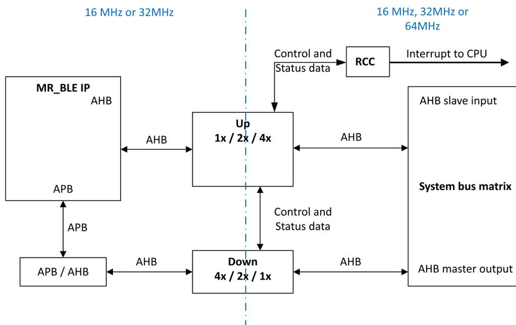
The management of data transfer versus clock domain and possible clock switch request is done using state machines:
- • one for the AHB master up converter
- • one for the AHB slave down converter
When a CPU/system clock frequency switch is needed (activate or deactivate the divider by two or four between the system and the MR_BLE), the user must request the new system clock targeted frequency in the RCC_CSCMDR.REQUEST bit (see Section 6.6.6: Clock switch command register (RCC_CSCMDR) for details).
When receiving a new divider ratio to apply (from the RCC), the AHBUPCONV block:
- • Informs the AHBDOWNCONV block (managing the APB transfer from the CPU to the MR_BLE APB registers)
- • Checks the traffic on the AHB bus between MR_BLE and CPU:
- – if no transfer is on-going, it uses the HREADY signal on the bus to hold any potential transaction that could occur during the clock frequency switch
Note: To respect the AHB lite protocol, the HREADY signal is fallen down only after the address phase of a new transfer, the new transfer phase data being stored internally in the converter.
If an AHB transfer is on-going, it waits until the current AHB transfer ends and then holds the AHB traffic as explained above.
- • In parallel, the AHBDOWNCONV block does the same action to hold any new transfer on the slave path of the data path (CPU access to MR_BLE APB registers).
- • Once the AHBUPCONV block has held its AHB line and has the confirmation from the AHBDOWNCONV, the other AHB2APB data path is also safely held; it allows the RCC block to change the system clock frequency to the requested one.
- • When the new system clock frequency is stable, the RCC informs the AHBUPCONV it is done. Then:
- – the AHBUPCONV releases the AHB transfers
- – the AHBUPCONV informs the AHBDOWNCONV that it can also release the AHB/APB transfers.