2. System and memory overview
2.1 System architecture
The main system consists of a 32-bit multilayer AHB bus matrix that interconnects:
- • Three masters:
- – CPU (Cortex®-M0+) core S-bus
- – DMA1
- – Radio system
- • Nine slaves:
- – Internal flash memory on CPU (Cortex®-M0+) S bus
- – Internal SRAM0 (16 Kbytes)
- – Internal SRAM1 (16 Kbytes)
- – Internal SRAM2 (16 Kbytes)
- – Internal SRAM3 (16 Kbytes)
- – APB0 peripherals (through an AHB to APB bridge)
- – APB1 peripherals (through an AHB to APB bridge)
- – AHB0 peripherals
- – AHBRF including AHB to APB bridge and radio peripherals (connected to APB2)
The bus matrix provides access from a master to a slave, enabling concurrent access and efficient operation even when several high-speed peripherals work simultaneously. This architecture is shown in Figure 1. STM32WB07xC and STM32WB06xC system architecture .
The system consists of a Cortex®-M0+ “Radio protocol and application” processor with its radio sub-system.
There is a single Flash memory to be used by the CPU for both Bluetooth protocol and application management.
The peripherals are located on the different system buses (AHB, APB0, APB1, APB2 for the radio system). There are 4 SRAM banks, an SRAM0 always power supplied and three SRAM (SRAM1, SRAM2 and SRAM3) that can be programmed to be always on or switchable. For more information see Section 5.7.2: Control register 2 (PWRC_CR2) .
Figure 1. STM32WB07xC and STM32WB06xC system architecture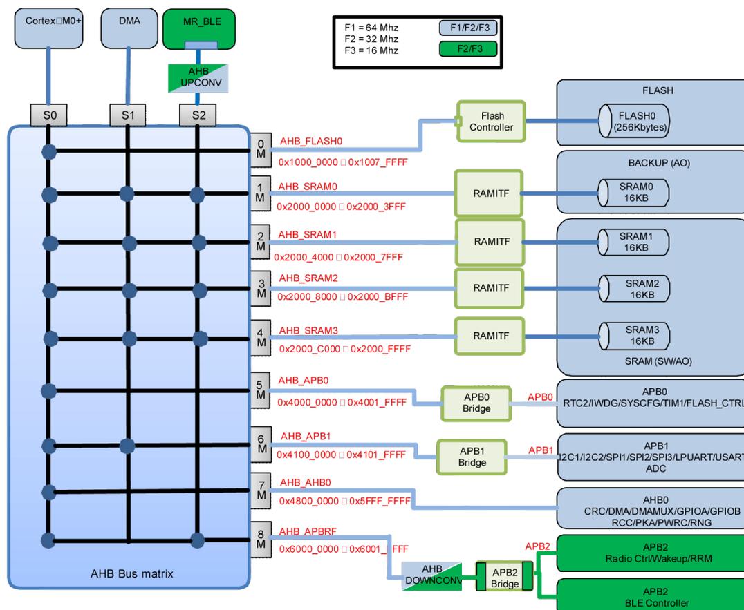
Frequency selection options:
- F1 = 64 Mhz
- F2 = 32 Mhz
- F3 = 16 Mhz
Selection buttons: F1/F2/F3 , F2/F3
Slave interfaces and address ranges:
- S0 (Cortex-M0+): AHB_FLASH0 (0x1000_0000 - 0x1007_FFFF), AHB_SRAM0 (0x2000_0000 - 0x2000_3FFF), AHB_SRAM1 (0x2000_4000 - 0x2000_7FFF), AHB_SRAM2 (0x2000_8000 - 0x2000_BFFF), AHB_SRAM3 (0x2000_C000 - 0x2000_FFFF), AHB_APB0 (0x4000_0000 - 0x4001_FFFF), AHB_APB1 (0x4100_0000 - 0x4101_FFFF), AHB_AHB0 (0x4800_0000 - 0x5FFF_FFFF), AHB_APBREF (0x6000_0000 - 0x6001_FFFF).
- S1 (DMA): AHB_SRAM0, AHB_SRAM1, AHB_SRAM2, AHB_SRAM3, AHB_APB1.
- S2 (MR_BLE via AHB_UPCONV): AHB_SRAM0, AHB_SRAM1, AHB_SRAM2, AHB_SRAM3, AHB_APB2.
- S3-S7: Unused.
Peripherals connected:
- FLASH: FLASH0 (256Kbytes) via Flash Controller.
- BACKUP (AO): SRAM0 16KB via RAMITF.
- SRAM1: SRAM1 16KB via RAMITF.
- SRAM2: SRAM2 16KB via RAMITF.
- SRAM3: SRAM3 16KB via RAMITF. SRAM (SW/AO).
- APB0: RTC2/IWDG/SYSCFG/TIM1/FLASH_CTRL via APB0 Bridge.
- APB1: I2C1/I2C2/SPI1/SPI2/SPI3/LPUART/USART/ADC via APB1 Bridge.
- APB2: Radio Ctrl/Wakeup/RRM and BLE Controller via APB2 Bridge (connected to AHB_DOWNCONV).
- AHB0: CRC/DMA/DMAMUX/GPIOA/GPIOB/RCC/PKA/PWRC/RNG.
2.1.1 S0: CPU (Cortex ® -M0+) S-bus
This bus connects the system bus of the CPU core to the BusMatrix. This bus is used by the core to fetch instructions, for literal load and debug access, and access data located in a peripheral or SRAM area. The targets of this bus are all the possible peripherals (the internal flash and SRAM memories, the AHB0, APB0, APB1 and APB2 peripherals).
2.1.2 S1: DMA-bus
This bus connects the AHB master interface of the DMA to the BusMatrix. The targets of this bus are the four banks of SRAM and the APB1 peripheral.
2.1.3 S2: Radio system-bus
This bus connects the AHB master interface of the radio system to the BusMatrix. The targets of this bus are the four banks of SRAM and the APB2 peripherals (internal APB blocks of the MR_BLE/Radio sub-system IP).
2.1.4 BusMatrix
The BusMatrix manages the access arbitration between masters. The arbitration uses a "Round Robin" algorithm. The BusMatrix is composed of three masters (CPU, DMA1-bus and radio system-bus) and nine slaves (FLASH, SRAM0, SRAM1, SRAM2 & SRAM3, APB0 and APB1, AHB0 and AHBRF).
AHB/APB bridges
The two bridges AHB to APB0 and AHB to APB1 provide full synchronous connections between the AHB and the two APB buses.
The bridge AHB to APB2 provides synchronous connections between the AHB and the APB bus. Two blocks are added to the AHB/APB path to manage potential prescaled MR_BLE frequency versus the system frequency:
- • AHB up converter is used for the MR_BLE AHB master transactions towards the SRAM
- • AHB down converter is used for the CPU AHB master transactions towards the MR_BLE APB registers.
Refer to Section 2.2.2: Memory map and register boundary addresses for the address mapping of the peripherals connected to this bridge.
After each device reset, all peripheral clocks are disabled (except for the SRAM and Flash memory interface). Before using a peripheral the user has to enable its clock in the RCC_AHBxENR and the RCC_APBxENR registers.
Note: When a 16- or 8-bit access is performed on an APB register, the access is transformed into a 32-bit access: the bridge duplicates the 16- or 8-bit data to feed the 32-bit vector.
2.2 Memory organization
2.2.1 Introduction
Program memory, data memory and registers are organized within the same linear 4-Gbyte address space.
These bytes are coded in memory in Little Endian format. The lowest numbered byte in a word is considered the word least significant byte and the highest numbered byte the most significant.
Figure 2. Memory map
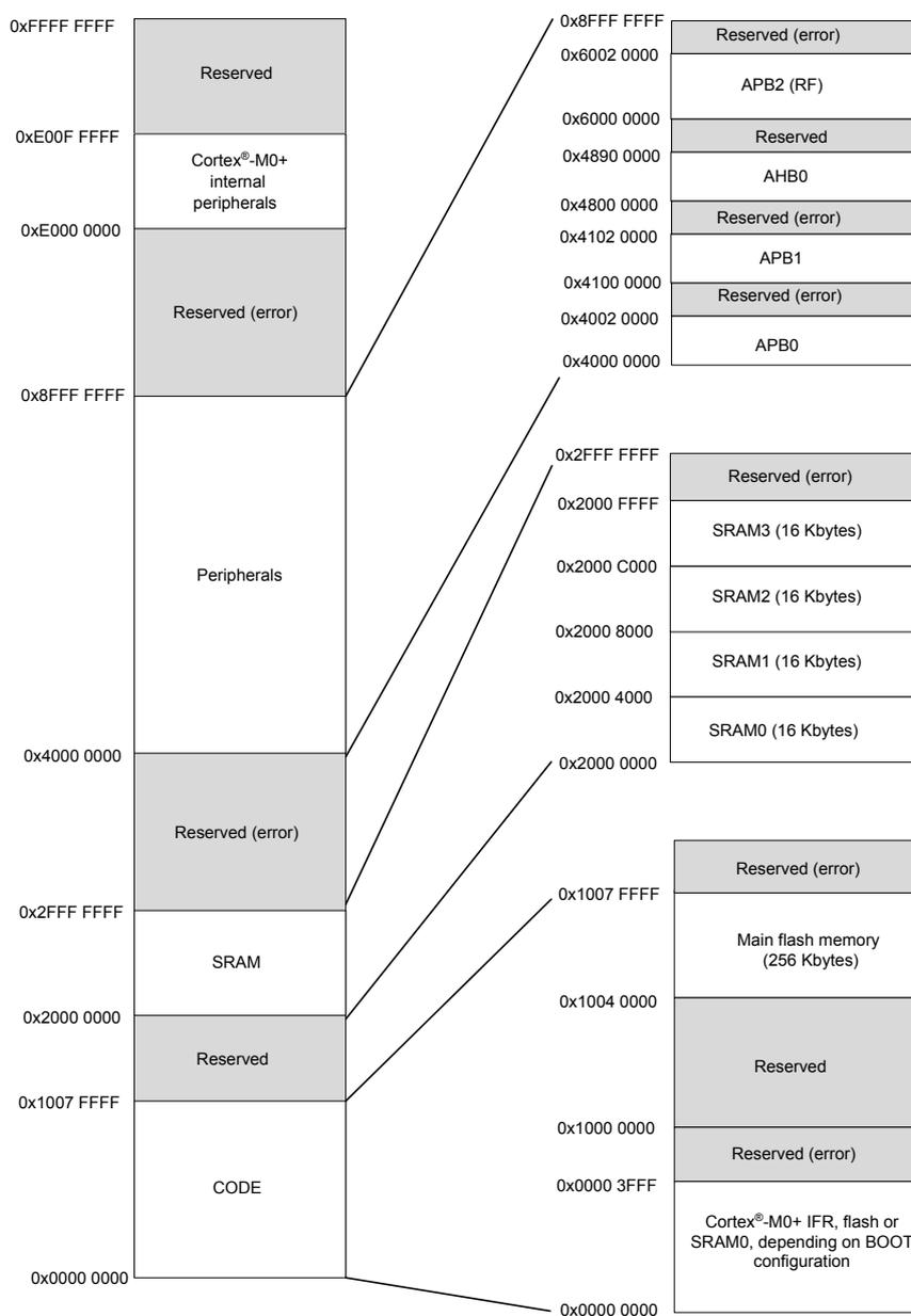
The diagram illustrates the memory map for a Cortex-M0+ microcontroller, showing the allocation of memory addresses to various system components. The memory is divided into several regions: CODE, SRAM, Reserved, and Peripherals. The CODE region starts at 0x0000 0000 and ends at 0x1007 FFFF. The SRAM region starts at 0x1008 0000 and ends at 0x2000 0000. The Reserved region starts at 0x2000 0000 and ends at 0x4000 0000. The Peripherals region starts at 0x4000 0000 and ends at 0x8FFF FFFF. The Cortex-M0+ internal peripherals are located in the address range 0xE000 0000 to 0xE00F FFFF. The APB0, APB1, and APB2 (RF) peripherals are located in the address range 0x4000 0000 to 0x6002 0000. The SRAM0, SRAM1, SRAM2, and SRAM3 are located in the address range 0x2000 4000 to 0x200F FFFF. The Main flash memory is located in the address range 0x1004 0000 to 0x1007 FFFF. The Cortex-M0+ IFR, flash or SRAM0, depending on BOOT configuration, is located in the address range 0x0000 3FFF to 0x0000 0000.
| Address Range | Memory Type / Content |
|---|---|
| 0x0000 0000 – 0x1007 FFFF | CODE |
| 0x1008 0000 – 0x2000 0000 | SRAM |
| 0x2000 0000 – 0x4000 0000 | Reserved (error) |
| 0x4000 0000 – 0x8FFF FFFF | Peripherals |
| 0xE000 0000 – 0xE00F FFFF | Cortex®-M0+ internal peripherals |
| 0xE000 0000 – 0xE00F FFFF | Reserved (error) |
| 0x0000 0000 – 0x0000 3FFF | Cortex®-M0+ IFR, flash or SRAM0, depending on BOOT configuration |
| 0x1000 0000 – 0x1000 3FFF | Reserved (error) |
| 0x1004 0000 – 0x1007 FFFF | Main flash memory (256 Kbytes) |
| 0x1008 0000 – 0x2000 0000 | Reserved |
| 0x2000 0000 – 0x2000 4000 | SRAM0 (16 Kbytes) |
| 0x2000 4000 – 0x2000 8000 | SRAM1 (16 Kbytes) |
| 0x2000 8000 – 0x2000 C000 | SRAM2 (16 Kbytes) |
| 0x2000 C000 – 0x2000 FFFF | SRAM3 (16 Kbytes) |
| 0x2000 FFFF – 0x2FFF FFFF | Reserved (error) |
| 0x4000 0000 – 0x4100 0000 | APB0 |
| 0x4100 0000 – 0x4102 0000 | Reserved (error) |
| 0x4102 0000 – 0x4800 0000 | APB1 |
| 0x4800 0000 – 0x4890 0000 | Reserved (error) |
| 0x4890 0000 – 0x6000 0000 | AHB0 |
| 0x6000 0000 – 0x6002 0000 | Reserved |
| 0x6002 0000 – 0x600F FFFF | APB2 (RF) |
| 0x6010 0000 – 0x6FFF FFFF | Reserved (error) |
DT/00198
All the memory areas that are not allocated to on-chip memories and peripherals are considered “Reserved”. For the detailed mapping of available memory and registers areas, refer to Section 2.2.2: Memory map and register boundary addresses and to each peripheral register map section.
2.2.2 Memory map and register boundary addresses
Table 3. STM32WB07xC and STM32WB06xC memory map and peripheral register boundary addresses gives the boundary addresses of the peripherals available in the device.
Table 3. STM32WB07xC and STM32WB06xC memory map and peripheral register boundary addresses
| Bus | Boundary address | Actual size (bytes) | Peripheral | Peripheral register map |
|---|---|---|---|---|
| Misc | 0xE010 0800 - 0xFFFF FFFF | 255 M | Reserved | - |
| 0xE000 0000 - 0xE00F FFFF | 1 M | Private peripheral bus | Cortex-M0+ registers (interrupt controller, SysTick, etc.) | |
| APB2 | 0x6000 1800 - 0x6000 1BFF | 1 K | WAKEUP | Wakeup registers of the MR_BLE |
| 0x6000 1500 - 0x6000 17FF | 1 K | Radio registers | Radio registers through APB direct access | |
| 0x6000 1400 - 0x6000 14FF | RRM | RRM registers of the MR_BLE | ||
| 0x6000 1000 - 0x6000 13FF | 1 K | RADIO_CTRL | Radio controller registers of the MR_BLE | |
| 0x6000 0000 - 0x6000 00FF | 256 | BLE | BLE link layer registers of the MR_BLE | |
| AHB0 | 0x4880 0000 - 0x4880 03FF | 1 K | DMAMUX | See Table 29. DMAMUX register map and reset values |
| 0x4870 0000 - 0x4870 00FF | 256 | DMA slave | See Table 26. DMA register map and reset values | |
| 0x4860 0000 - 0x4860 03FF | 4 K | RNG | See Table 1 | |
| 0x4850 0000 - 0x485F FFFF | 156 | PWRC | See Table 11. PWRC register map | |
| 0x4840 0000 - 0x484F FFFF | 156 | RCC | See Section 6.6.18: RCC register map | |
| 0x4830 0400 - 0x4830 07FF | 1 K | PKA RAM | Table 3. STM32WB07xC and STM32WB06xC memory map and peripheral register boundary addresses | |
| 0x4830 0000 - 0x4830 03FF | 1 K | PKA slave | ||
| 0x4820 0000 - 0x4820 03FF | 1 K | CRC | See Table 41. CRC register map and reset values | |
| 0x4810 0000 - 0x4810 03FF | 1 K | GPIOB | See Section 7.4.11: GPIO register map | |
| 0x4800 0000 - 0x4800 03FF | 1 K | GPIOA | See Section 7.4.11: GPIO register map | |
| APB1 | 0x4100 7000 - 0x4100 73FF | 1 K | SPI3 | See Section 22.9.10: SPI/I2S register map |
| 0x4100 6000 - 0x4100 60FF | 256 | ADC | See Section 12.6.23: ADC registers map | |
| 0x4100 5000 - 0x4100 53FF | 1 K | LPUART | See Section 21.5: LPUART registers | |
| 0x4100 4000 - 0x4100 43FF | 1 K | USART | See Section 20.7: USART registers | |
| 0x4100 3000 - 0x4100 33FF | 1 K | SPI2 | See Section 22.9.10: SPI/I2S register map | |
| 0x4100 2000 - 0x4100 23FF | 1 K | SPI1 | See Section 22.9.10: SPI/I2S register map | |
| 0x4100 1000 - 0x4100 13FF | 1 K | I2C2 | See Section 19.6.12: I2C register map | |
| 0x4100 0000 - 0x4100 03FF | 1 K | I2C1 | See Section 19.6.12: I2C register map | |
| APB0 | 0x4000 4000 - 0x4000 43FF | 1 K | RTC | See Section 17.6.14: RTC register map |
| 0x4000 3000 - 0x4000 33FF | 1 K | IWDG | See Section 18.4.6: IWDG register map | |
| 0x4000 2000 - 0x4000 23FF | 1 K | TIM1 | See Section 16.4.24: TIM1 register map | |
| 0x4000 1000 - 0x4000 1FFF | 4 K | FLASH_CTRL | See Section 9.3: Flash controller register map | |
| 0x4000 0000 - 0x4000 003F | 64 | SYSTEM_CTRL | See Section 8.2.17: System controller register map | |
| SRAM | 0x2000 C000 - 0x2000 FFFF | 16 K | SRAM3 | - |
| 0x2000 8000 - 0x2000 BFFF | 16 K | SRAM2 | - | |
| 0x2000 4000 - 0x2000 7FFF | 16 K | SRAM1 | - | |
| 0x2000 0018 - 0x2000 3FFF | 16360 | SRAM0 | - | |
| 0x2000 0000 - 0x2000 0017 | 24 | - | ||
| Flash | 0x1004 0000 - 0x1007 FFFF | 256 K | Main flash | - |
| OTP | 0x1000 1800 - 0x1000 1BFF | 1 K | OTP area | - |
| Bus | Boundary address | Actual size (bytes) | Peripheral | Peripheral register map |
|---|---|---|---|---|
| Boot (1) | 0x0000 0000 - 0x0000 3FFF | 16 K | CPU boot area | Mirroring of Flash or SRAM0 |
- 1. This area is a mirroring area. The CPU accesses are redirected to other memory map depending on REMAP and PREMAP bits located in the Flash controller CONFIG register. See Table 5. Address remapping depending on REMAP bit for remapping detail.
| Address | Actual size (bytes) | Identifier | Description |
|---|---|---|---|
| 0x2000 0000 | 4 | Reserved1 | Reserved for future use. |
| 0x2000 0004 | 4 | Reserved2 | Reserved for future use. |
| 0x2000 0008 | 4 | SavedMSP | Used by lpm module. Used to save context information pointer. |
| 0x2000 000C | 4 | WakeupFromSleepFlag | Used by lpm module. Indicate whether the system has been woken up from DeepStop. |
| 0x2000 0010 | 4 | ResetReason | Copy of last reset reason from register RCC_CSR. The register is read, copied to this location by the bootloader code and finally cleared. As a consequence, software reading the register always reads 0. Users should read this location to know the last reset reason. |
| 0x2000 0014 | 4 | AppBase | Relocation of application base. Bootloader jumps to the location pointed to by this value when a wakeup from DeepStop occurs. |
| 0x2000 00C0 | CFG_NUM_RADIO_TASKS*92+28 | Blue Core Config | Only when radio is used and radio clock is activated. NOTE: CFG_NUM_RADIO_TASKS is the number of simultaneous radio tasks selected by the application (radio controller supports up to 128 simultaneous radio tasks, but actual usable max value depends on the available RAM). |
SRAM0 memory locations from 0x2000 0000 to 0x2000 0017 are reserved for system use and users are not allowed to use these locations for their application.
Table 5. Address remapping depending on REMAP bit| REMAP | Memory mapped |
|---|---|
| 0 | Main flash |
| 1 | SRAM0 |
2.3 Arm ® Cortex ® -M0+
The Arm ® Cortex ® -M0+ processor was developed to provide a low-cost platform that meets the needs of MCU implementation, with a reduced pin count and low-power consumption, while delivering outstanding computational performance and an advanced response to interrupts.
The embedded Cortex-M0+ embeds:
- • four breakpoints
- • two watchpoints
- • an MPU (memory protection unit) providing eight unified protection regions
- • a SysTick running only with the system clock (external clock option not supported)
2.3.1 CPU memory remap
Following a CPU boot the application software can modify the memory map at address 0x0000 0000. This modification is performed by programming the REMAP bit in the flash controller (see Section 9.4.2: Configuration register (CONFIG) ).
The following memory can be remapped:
- • Main flash memory
- • SRAM0 memory
Embedded boot loader
ST provides a boot loader executed after each CPU reboot. This boot loader has its own documentation.
Note: The STM32WB07xC and STM32WB06xC device latches the PA8 / PA9 / PA10 / PA11 pads value at POR. The information is available in the PWRC_SR2 register (see Section 5.7.6: Status register 2 (PWRC_SR2) ). One of those four I/Os can be used by the boot loader as boot indication between a normal boot or a boot on serial interface.
2.3.2 Interrupts
Interrupts are handled by the Cortex-M0+ nested vector interrupt controller (NVIC). The NVIC controls specific Cortex-M0+ interrupts (address 0x00 to 0x3C) as well as 32 user interrupts (address 0x40 to 0xBC). In the STM32WB07xC and STM32WB06xC devices, the user interrupts have been connected to the interrupt signals of the different peripherals (GPIO, Flash controller, timers, UART,...). These interrupts can be controlled using the ISER, ICER, ISPR and ICOR registers.
Vector table
On reset, the Cortex-M0+ vector table is fixed at address 0x0000_0000. The software may relocate the vector table address to a different memory location, in a range 0x0000_0000 to 0xFFFF_FF80 in multiples of 256 bytes through the vector table offset register (VTOR) located in the Cortex-M0+ registers area.
The interrupt mapping for the vector table of the STM32WB07xC and STM32WB06xC devices is described in Table 6. Interrupt vectors.
Table 6. Interrupt vectors
| Position | Priority | Type of priority | Acronym | Description | Address offset |
|---|---|---|---|---|---|
| - | - | Initial main SP | 0x0000_0000 | ||
| - | -3 | Fixed | Reset | Reset_Handler | 0x0000_0004 |
| - | -2 | Fixed | NmiISR | NMI_Handler | 0x0000_0008 |
| - | -1 | Fixed | FaultISR | HardFault_handler | 0x0000_000C |
| - | - | RESERVED | RESERVED | RESERVED | 0x0000_000C - 0x0000_0038 |
| - | 6 | Settable | SysTick | System tick timer | 0x0000_003C |
| 0 | Init 0 | Settable | NVM | Non-volatile memory (Flash) controller | 0x0000_0040 |
| 1 | Init 0 | Settable | RCC | Reset and clock controller | 0x0000_0044 |
| 2 | Init 0 | Settable | BATTERY | PVD | 0x0000_0048 |
| 3 | Init 0 | Settable | I2C1 | I2C1 interrupt | 0x0000_004C |
| 4 | Init 0 | Settable | I2C2 | I2C2 interrupt | 0x0000_0050 |
| 5 | Init 0 | Settable | SPI1 | SPI1 interrupt | 0x0000_0054 |
| 6 | Init 0 | Settable | SPI2 | SPI2 interrupt | 0x0000_0058 |
| 7 | Init 0 | Settable | SPI3 | SPI3 interrupt | 0x0000_005C |
| 8 | Init 0 | Settable | USART | USART interrupt | 0x0000_0060 |
| 9 | Init 0 | Settable | LPUART | LPUART interrupt | 0x0000_0064 |
| 10 | Init 0 | Settable | TIM1 | TIM1 interrupt | 0x0000_0068 |
| 11 | Init 0 | Settable | RTC | RTC interrupt | 0x0000_006C |
| 12 | Init 0 | Settable | RESERVED | RESERVED | 0x0000_0070 |
| 12 | Init 0 | Settable | ADC | ADC interrupt | 0x0000_0070 |
| 13 | Init 0 | Settable | PKA | PKA interrupt | 0x0000_0074 |
| 14 | Init 0 | Settable | - | - | 0x0000_0078 |
| 15 | Init 0 | Settable | GPIOA | GPIOA interrupt | 0x0000_007C |
| 16 | Init 0 | Settable | GPIOB | GPIOB interrupt | 0x0000_0080 |
| 17 | Init 0 | Settable | DMA | DMA interrupt | 0x0000_0084 |
| 18 | Init 0 | Settable | BLE_TXRX (1) | BLE end of transfer interrupt | 0x0000_0088 |
| 19 | Init 0 | Settable | - (1) | - | 0x0000_008C |
| 20 | Init 0 | Settable | - (1) | - | 0x0000_0090 |
| 21 | Init 0 | Settable | RADIO_CTRL (1) | Radio control slow clock measurement interrupt | 0x0000_0094 |
| Position | Priority | Type of priority | Acronym | Description | Address offset |
|---|---|---|---|---|---|
| 22 | Init 0 | Settable | MR_BLE (1) | RRM and radio FSM interrupt | 0x0000_0098 |
| 23 | Init 0 | Settable | CPU_WKUP (1) | CPU wakeup interrupt | 0x0000_009C |
| 24 | Init 0 | Settable | BLE_WKUP (1) | BLE wakeup interrupt | 0x0000_00A0 |
| 25 | Init 0 | Settable | BLE_SEQ | BLE RX/TX sequence interrupt | 0x0000_00A4 |
| 26 - 31 | Init 0 | Settable | - | RESERVED | 0x0000_00A8 - 0x0000_00BC |
- 1. Some specific cares are needed at SW level to clear the interrupt: see Warning for interrupt clearance when system clock is faster than MR_BLE clock .
Interrupt activation sequence
Safely activating a peripheral interrupt requires the following steps:
- • make sure the interrupt is disabled and cleared on the peripheral side (this prevents receiving an interrupt due to a previous event)
- • clear pending requests for this interrupt on the Cortex-M0+ side using the NVIC ICPR register
- • set the priority using the NVIC IPR0-IPR7 registers
- • activate on the Cortex-M0+ side using the NVIC ISER register
- • activate on the peripheral side
Note that most peripherals require clearing interrupt requests on the peripheral side when handling interrupt service requests to prevent triggering continuous interrupts for the same event.
For more details on the Cortex-M0+ exception model, see “ARMv6-M Architecture Reference Manual”, §B1.5.
For more details on the Cortex-M0+ NVIC behavior and registers, see “ARMv6-M Architecture Reference Manual”, §B3.4.