25. Radio IP
25.1 Overview
This section describes the Radio IP embedded in the STM32WB05xZ product. The Radio controller MR_BLE manages the Bluetooth® LE protocol with hardware addon to support some new Bluetooth specification features, and controls the RF analog module.
25.1.1 Architecture overview of the MR_BLE IP
As shown in Figure 197. RRM overview , the MR_BLE IP contains:
- • A Bluetooth® LE subsystem dedicated to Bluetooth protocol (IP_BLE block) and containing:
- – a Bluetooth® LE link layer. This sub block is an AHB master
- – a demodulator
- – a modulator
- • An RRM (radio resource manager) block contains:
- – a UDRA (unified direct register access) executing link list command in RAM to read/write radio register. This sub-block is an AHB master
- – Direct radio register access allowing read/write access to radio registers through APB
- • A wakeup/always-on block contains:
- – a wakeup block for IP_BLE including a time interpolator and sleep request / wakeup request management and a few enhanced features
- • A radio FSM controlling the RF2G4 analog radio.
- • A radio registers block (to program the analog radio parameters).
- • Some small blocks used for calibrations, PLL control, Rx data path interface (AGC, FIFO ADC).
The MR_BLE IP supports two system clock frequencies: 16 MHz and 32 MHz.
Figure 196. MR_BLE architecture overview
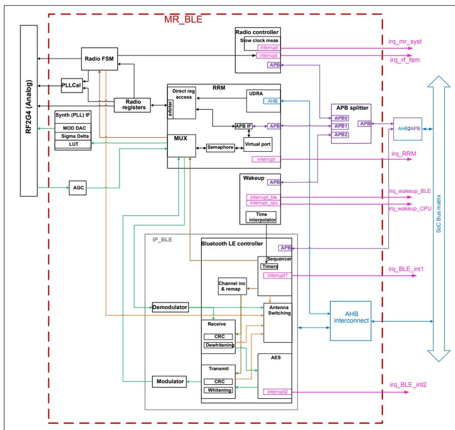
The diagram illustrates the MR_BLE architecture, enclosed in a dashed red box labeled 'MR_BLE'. On the left, an 'RF2G4 (Analog)' block connects to a 'PLLCal', 'Synth (PLL) IF', 'MOD DAC', 'Sigma Delta LUT', and 'AGC'. These connect to a 'Radio FSM' and 'Radio registers'. The 'Radio FSM' connects to a 'Radio controller' which has 'Slow clock meas' and 'interrupt' outputs ('irq_mr_syst', 'irq_rf_fsm'). The 'Radio registers' connect to a 'MUX' and 'RRM' (RRM, UDRA, APB IF, Semaphore, Virtual port). The 'MUX' connects to 'IP_BLE' (Bluetooth LE controller, Sequencer, Timers, Channel inc & remap, Antenna Switching, AES, Demodulator, Modulator). The 'IP_BLE' has 'interrupt' outputs ('irq_BLE_int1', 'irq_BLE_int2'). A 'Wakeup' block (Wakeup, Time interpolator) connects to the 'MUX' and has 'interrupt' outputs ('irq_wakeup_BLE', 'irq_wakeup_CPU'). An 'APB splitter' (APB0, APB1, APB2) connects to the 'RRM' and 'IP_BLE' and to an 'AHB2APB' block. The 'AHB2APB' connects to an 'AHB interconnect', which is part of a 'SoC Bus matrix' (indicated by a large blue double-headed arrow on the right).
25.1.2 Global scenario for Bluetooth® LE protocol usage
The Bluetooth® LE link layer always needs a trigger event to start a sequence. This trigger event has three possible timer sources (wakeup timer, Timer1, or Timer2).
Basically, a Bluetooth sequence follows the steps described below:
- 1. The CPU needs to prepare in RAM (through different tables) all information needed for the coming transfer:
- – for radio programming (channel number, reception, or transmission, calibration feature, etc.)
- – for a packet to transmit or receive (contents, ADV, or data, encryption, etc.)
- – for interrupt mask selection
- – to prepare the trigger event that schedules the sequence after this one
- 2. Then the CPU has to program the chosen timer (except if already done through a table for timer2 inside the previous sequence).
- 3. Once the Bluetooth® LE link layer receives the trigger event from the programmed timer, it gets all the information in the RAM table and launches the requested transfer.
- 4. At the end of the sequence (and not before), the Bluetooth® LE link layer writes back in RAM tables some information, updates the status/error flags and generates an interrupt towards the CPU according to the interrupt mask programming.
- 5. The CPU has to treat the RAM table updated information (including packet payload after a reception) to decide what is the next wanted sequence. Then a cycle restarts from step 1.
Note:
- • The RAM tables are located in a retention area. So, the data is kept even during low-power modes that switch off the digital 1.2 V power domain. This allows the Bluetooth® LE link layer to start a transmission/reception while the CPU is not yet available as rebooting from a wakeup reset.
25.1.3 Miscellaneous features: RF activity monitoring
25.1.3.1 On-going Tx sequence information (to control an external power amplifier (PA))
The MR_BLE is able to control an external power amplifier (located on the board to increase the Tx power) through a signal provided to the SoC to be connected directly on an external GPIO or to be managed with an additional logical mechanism. The external PA can be useful to extend the Tx power.
The external power amplifier components have quite a long latency to establish and consume a lot of current (several mA) which could lead to unlocking the MR_BLE PLL. For this reason, the control signal is anticipated as soon as the system knows it starts a Tx sequence and stops as soon as possible (at the same time as the internal PA).
The MR_BLE outputs a signal to the SoC, which is high as soon as a Tx sequence is requested to the radio FSM up to the return to ACTIVE2 or less state. To be more precise, the information is provided as soon as the radio FSM is starting to treat a Tx request (leaving ACTIVE2 state for EN_LDO state) and goes down as soon as the system switches off the internal PA (for example, leaving Tx state at the end of the transmission or during EN_PA in case of PLL lock fail).
The information is available in two different ways in the STM32WB05xZ:
- • directly output on a GPIO (RADIO_TX_SEQUENCE)
- • flags and associated interrupt available in the system controller (SYSCFG block)
25.1.3.2 On-going Rx sequence information (to control an external low noise amplifier (LNA))
The MR_BLE is able to control an external low noise amplifier (located on the board) through a signal provided to the SoC to be connected directly on an external GPIO or to be managed with additional logical mechanism.
The MR_BLE outputs a signal to the SoC, which is high as soon as an Rx sequence is requested to the radio FSM up to the return to ACTIVE2 or less state.
The information is available in two different ways in the STM32WB05xZ:
- • directly output on a GPIO (RADIO_RX_SEQUENCE)
- • flags and associated interrupt available in the system controller (SYSCFG block).
25.1.3.3 RF activity information
An additional signal is available on the device pin to inform either an Rx or a Tx sequence is active. This pin called RADIO_RF_ACTIVITY is a logical OR between the RADIO_TX_SEQUENCE and RADIO_RX_SEQUENCE mentioned in the two previous sections.
25.1.4 Bluetooth® LE standard 5.1 additional support
The STM32WB05xZ Radio IP supports the angle of arrival (AoA) and angle of departure (AoD) feature by managing:
- • the constant tone extension (CTE) inside the packet
- • the antenna switching mechanism for both AoA and AoD
In transmission, the MR_BLE is able:
- • to append the constant tone extension at the end of the packet
- • and, if AoD mode is selected, to manage the antenna switching according to CTEInfo parameters (duration and switching slots definition) and following a pattern provided by the SW
- • The SW has to provide to the IP_BLE the CTE information (CTE time, CTE type, slot width) and the antenna pattern if antenna switching in AoD has to be managed
In reception, the MR_BLE is able:
- • to detect and decode CTEInfo bit field from the received frame
- • to store the IQ samples in RAM according to sampling time slots
- • and, if AoA mode is selected, manage the antenna switching according to CTEInfo parameters (duration and switching slots definition)
The SW has only to provide the slot width information if the configuration is an AoA configuration as this is the only information not available in the received frame and the antenna pattern.
The CTE/antenna switching mechanism of the MR_BLE provides to the external world a 7-bit antenna identifier (ANT_ID[6:0]) indicating the antenna number to be used.
The CTE/antenna switching feature implies:
- • adding few bit fields in the RAM tables
- – CTE information when hardware cannot extract them by itself
- – A pointer on a RAM buffer where to store the IQ sampling for CTE reception
- – Antenna pattern length and a pointer on the RAM buffer containing the antenna pattern
- • adding a status register in the IP_BLE APB registers (STATUS2REG) providing information on the IQ sampling and antenna switching sequence that just occurred
- • adding some radio registers to tune timing delays on antenna switching control and IQ sampling
Those new features support can be disabled by SW through the StatMach.CTEDisable bit.
25.2 Interfacing with the MR_BLE IP
The MR_BLE IP interfaces with several blocks in the system:
- • CPU through interrupts
- • RAM through an AHB interface either initiated by the RRM or by the Bluetooth® LE link layer
- • Power controller block and clock and reset controller block
- • Specific signals to propagate to the pads of the device to manage inside the Soc.
25.2.1 Interruption lines to the CPU
The MR_BLE IP provides several interruption lines to the CPU, issued by different sub-blocks:
- • 2 interrupt lines from the Bluetooth® LE link layer
- • 2 interrupt lines from the wakeup block
- • 1 interrupt line from the RRM
- • 2 interrupt lines from the radio controller.
Table 115. Interruption summary
| Line number on SoC NVIC | Interrupt name | Description |
|---|---|---|
| 18 | BLE_TXRX (int_BLE_irq1) | Indicate that a Bluetooth sequence occurred |
| 19 | BLE_AES (int_BLE_irq2) | Indicate that an AES LE privacy or manual operation ended |
| 21 | RADIO_CTRL (int_mr_syst) | Indicate that the slow clock measurement result is ready |
| 22 | MR_BLE (irq_rrm + irq_radio_fsm) | Combine information related to RRM-UDRA operations and radio FSM analog feedback (PLL lock and calibration) |
| 23 | CPU_WKUP (irq_wakeup_cpu) | Indicate a CPU wakeup timer match |
| 24 | BLE_WKUP (irq_wakeup_ble) | Indicate a wakeup timer trigger occurred on the sequencer |
25.2.1.1 IP_BLE interrupt lines
irq_BLE_int1 (aka BLE_TXRX):
- • This interrupt line is triggered when a Bluetooth sequence has been executed. It informs the CPU that status/error flags and RAM tables may have been updated
- • Mapped on CPU interrupt line 18.
irq_BLE_int2 (aka BLE_AES):
- • This interrupt line is dedicated to an embedded AES block and combines both AES LE privacy and AES manual encryption information
- • Mapped on CPU interrupt line 19.
See Section 25.8.3: IP_BLE interrupts for details on interrupt sources.
25.2.1.2 wakeup block interrupt lines
irq_wakeup_ble (aka BLE_WKUP):
- • This interrupt line indicates to the CPU that the IP_BLE receives a wakeup request from the MR_BLE IP wakeup block. The wakeup request source is the wakeup timer.
- • Mapped on CPU line 24
irq_wakeup_cpu:
- • This interrupt line indicates that the wakeup timer reaches the programmed value to trigger an interrupt towards the CPU (dedicated slice in the wakeup block design in parallel with the IP_BLE slice).
- • Mapped on CPU line 23.
See Section 25.9: Wakeup block for more details.
25.2.1.3 RRM interrupt line
This interrupt line is dedicated to the RRM block. It is triggered on semaphore and UDRA sub-block activities.
See Section 25.4: Radio resource manager (RRM) for more details.
25.2.1.4 Radio controller interrupt lines
irq_rf_fsm:
- • This interrupt line indicates events and errors detected by the radio state machine.
irq_mr_syst:
- • This interrupt line is dedicated to the counter measuring the slow clock period and frequency. It indicates when the calculated values are available.
See Section 25.7: Radio controller for more details.
25.2.2 Interface with the RAM embedded in the SoC
The MR_BLE IP is an AHB master on the bus matrix as the CPU or a DMA.
Two of its internal blocks access the RAM of the system:
- • the Bluetooth® LE link layer to read the sequence information and Tx/Rx configuration parameters, to read the data to transmit or to write the received data in the RAM tables, to store the IQ samples during a CTE reception
- • the RRM UDRA block to get commands structure in RAM, used to program the radio registers while the CPU is not available (potentially rebooting after a low-power mode).
Both internal blocks may need to access the RAM in parallel. An arbiter is located inside the IP.
25.2.3 Interface with the power clock and reset controllers
The MR_BLE receives several clocks from the SoC:
- • the system clock that can be 16 or 32 MHz
- • an always 16 MHz clock
- • an always 32 MHz clock
- • a slow clock (called 32 kHz clock in this document) that needs to be in the always-on power domain as it corresponds to the clock used to wake up the radio link layers from sleep state.
The fast clocks (system, 16 MHz, and 32 MHz) must be accurate when the radio is used (for the transmission/reception).
The MR_BLE IP communicates with the power controller of the system to indicate when the MR_BLE IP is ok to go to low-power modes and when it requests a wakeup.
The MR_BLE IP says it is ready to sleep when:
- • no sequence is on-going (a sequence starts with a trigger event and the IP_BLE interrupt rising edge)
- • no timer1 or timer2 selected to generate the next trigger event on the Sequencer
- • no pending interrupt in the INTERRUPT1REG APB register.
The MR_BLE IP also proposes an embedded always-on timer that may generate a programmed wakeup for the CPU.
25.3 Warning for users
Note:
- • If some radio registers are modified in the RRM commands, they should not be also modified by the CPU through direct access. Indeed, there is no way to keep coherency and know which master last modified the concerned radio register.
- • Accurate system clock must be present during all scenarios where the IP_BLE Sequencer uses the Timer1 (from trigger event).
- • On the fly, CCM encryption does not work if TxRxPack.NS_EN bit is low.
25.4 Radio resource manager (RRM)
The Radio Resource Manager (RRM) is a hardware block managing the radio access to one unique controller at a time.
It is the block that manages the requests performed by the Bluetooth® LE link layer of the IP_BLE and the CPU to access the radio resources. The requests pass through a semaphore and only one of the two can take control of the radio at a time. The arbitration behaves as follows:
- • check the priority value to choose between the IP_BLE or the CPU
- • if the same, then the arbiter eliminates the requester that has been served more recently.
The two controllers can request access to the radio resources through a dedicated port:
- • Port 0 for the IP_BLE
- • Port 1 for the CPU (it is a virtual port in this case)
The Bluetooth® LE link layer does not have access to the radio resources until it requests a token to the RRM and the RRM grants it. For the CPU, only RRM commands require to get a token, the direct APB access to the Radio registers is always possible. The token is requested by software for the CPU while it is done by hardware for the Bluetooth® LE link layer each time a timer trig event starts a sequence. Nevertheless, the firmware can release the token granted by the Bluetooth® LE link layer writing inside the CMDREG APB register. Once the requester has the token, its port is granted, and it can access the radio resources.
Figure 197. RRM overview
The diagram illustrates the internal architecture of the Radio Resource Manager (RRM) and its connections to external blocks. The RRM contains several key components:
- Radio FSM and RF2G4 : Connected to the top of the RRM.
- IP_BLE : An external block connected to the top of the RRM via a green line (token request/granting).
- Semaphore : A central component within the RRM that manages access. It receives green lines from IP_BLE and a purple line (APB transfer) from the CPU's virtual port.
- Direct reg access : An APB interface for the CPU to access radio registers directly. It is connected to the Radio registers and the APB IF .
- UDRA : A component with an AHB IF that receives blue lines (AHB transfer) from the CPU and sends dark orange lines (data path) to the RRM's internal logic.
- Virtual port (CPU) : An APB interface for the CPU to send RRM commands. It is connected to the APB IF and the Semaphore .
- RRM : The main block containing the internal logic, connected to the APB IF and the AHB IF .
- interrupt : A pink line output from the RRM to the CPU, labeled irq_RRM .
- A Soc Bus matrix connected to the RRM's APB IF and AHB IF via an AHB2APB bridge.
- RAM : Contains GlobalStatMach , @RadioConfigPtr , @port1-Command1 , and port1-Command1 . It is connected to the Soc Bus matrix .
- Blue: AHB transfer
- Purple: APB transfer
- Green: token request/granting
- Dark orange: data path
- Brown: UDRA command
- Pink: interrupt
25.4.1 Semaphore
The semaphore grants the access to the radio resources control to the radio controller or to the CPU depending on the demand.
An arbitration system is in place to manage conflicts when a token request is raised simultaneously by the IP_BLE controller and the CPU. In this case, the arbiter:
- • checks the priority programmed for the CPU virtual port to choose between the two requesters (IP_BLE has priority=0)
- • if the same, eliminates the requester that has been served more recently.
The CPU is a virtual port and must provide the token request through an APB registers bit field (see Section 25.4.4.1: RRM register list ). The Bluetooth® LE link layer controller uses hard wired signals to communicate with the RRM and the request is managed directly by the Bluetooth® LE link layer each time a timer trig event starts a Bluetooth® LE sequence.
As soon as the IP_BLE port is granted, the Radio FSM block is informed by the semaphore that the radio is about to be used. The goal is to switch off the analog as much as possible when not used and switch it on only when needed (for power consumption)
Some interruptions are linked to the semaphore block in the RRM:
- • on a port grant event
- • on a port release event
See Section 25.4.4: RRM registers .
25.4.2 UDRA
The "Unified Direct Register Access" block allows the software to prepare some commands in a command link list located in the retention RAM. Those commands execute read from and write into the radio registers.
Some interruptions are linked to the UDRA block in the RRM:
- • on a command start event
- • on a command end event.
See Section 25.4.4: RRM registers for more details.
The main goal of this block is to allow the Bluetooth® LE link layer to reinitialize the radio registers after a low power mode sequence to start an RF communication while the CPU is still being booted and not yet available to manage.
Note: The read command embeds some limitations. However, the radio registers can be read directly through the APB by the CPU so the read command of the UDRA is useless.
25.4.2.1 RAM command link list information
The mapping in RAM for the commands for each port is the following:
- • the RadioConfigPtr field of the GlobalStateMachGlobalStatMach contains the start address of the command start list (this address must be 32-bit aligned)
- • the command start list is a 32-bit element table containing the first command addresses of each command number of each port
- • each command of each port contains some read and/or write actions on radio registers.
An overview of this indirect mapping is represented in Figure 198. UDRA command list mapping in RAM (example)
Figure 198. UDRA command list mapping in RAM (example)
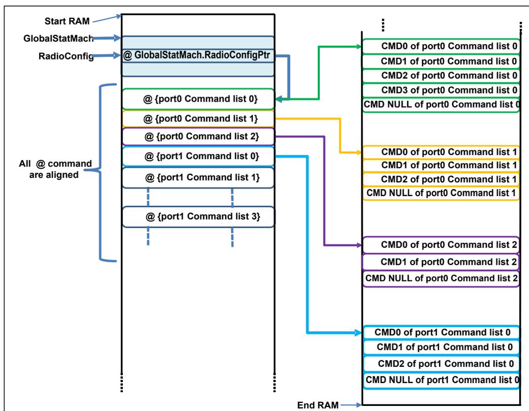
The RadioConfigPtr value is loaded by the RRM-UDRA automatically when the radio IP reset is released. If the software did not initialize this RAM address supposed to point on the command_start_list address before this first automatic load, a “reload pointer” command is available by writing 1 in the UDRA_CTRL0[0] APB register (this bit is auto-cleared immediately).
Note: The RadioConfigPtr pointer value loaded and used by the RRM-UDRA block can be read in the UDRA_RADIO_CFG_PTR APB register.
The port mapping has been defined as follows:
- • 2 ports (port0=IP_BLE, port1= VP_CPU)
- • port0 supports 3 commands (command 0/1/2)
- • port1 supports 4 commands (command 0/1/2/3)
This leads to a command start list table as presented below:
Table 116. Command start list details
| Address in RAM | Meaning | Comments |
|---|---|---|
| @RadioConfigPtr(value) + 0x00 | port0->command0 base address | Command requested by the Bluetooth® LE link layer on wakeup timer trigger event if RadioComListEna bit = 1 in on-going StateMach. |
| @RadioConfigPtr(value) + 0x04 | port0->command1 base address | Command requested by the Bluetooth® LE link layer on Timer1 trigger event if RadioComListEna bit = 1 in on-going StateMach. |
| @RadioConfigPtr(value) + 0x08 | port0->command2 base address | Command requested by the Bluetooth® LE link layer on Timer2 trigger event if RadioComListEna bit = 1 in on-going StateMach. |
| @RadioConfigPtr(value) + 0x0C | port1->command0 base address | VP_CPU: if the software needs to use an RRM-UDRA command to access the radio register instead of a direct access through APB. |
| Address in RAM | Meaning | Comments |
|---|---|---|
| @RadioConfigPtr(value) + 0x10 | port1->command1 base address | VP_CPU: if the software needs to use a second RRM-UDRA command to access the radio register instead of a direct access through APB. |
| @RadioConfigPtr(value) + 0x14 | port1->command2 base address | VP_CPU: if the software needs to use a third RRM-UDRA command to access the radio register instead of a direct access through APB. |
| @RadioConfigPtr(value) + 0x18 | port1->command3 base address | VP_CPU: if the software needs to use a fourth RRM-UDRA command to access the radio register instead of a direct access through APB. |
25.4.2.2 UDRA command format in RAM
The write and read command format are described in the following table. Note that only one radio register address is entered for a write or a read. Then, if the number of data to write/read is more than one, the address is incremented automatically by 1.
Table 117. UDRA command format in RAM
| Byte number | Address in RAM | Byte value | Description |
|---|---|---|---|
| 1 | command_base_addr | 0x-- | bit7: 0=write / 1=read bit[6:0] = number of data to write or to read. n = number of data for the example in this table. |
| 2 | command_base_addr+1 | 8-bit address | Address of a Radio register following the 8-bit address mapping (see Section 25.5.1: Radio register list ) |
| 3 | command_base_addr+2 | 1 st data | If write command: write first 8-bit data to be written. If read command: location where the first 8-bit read datum is available. |
| 4 | command_base_addr+3 | 2 nd data | Optional (depends on number of data to write/read). If write command: write second 8-bit data to be written. If read command: location where the second 8-bit read datum is available. |
| ... | |||
| n+2 | command_base_addr+(n+1) | n th data | Optional (depends on number of data to write/read). If write command: write n
th
8-bit data to be written. If read command: location where the n th 8-bit read datum is available. |
| n+3 | command_base_addr+n+2 | 0x-- | Optional: possible to chain other commands. bit7: 0=write / 1=readbit [6:0] = number of data to write or to read. |
| n+4 | command_base_addr+n+3 | 8-bit address | Address of a radio register following the 8-bit address mapping (see ) |
| n+5 | command_base_addr+n+4 | 1 st data | If write command: write first 8-bit data to be written. If read command: location where the first 8-bit read datum is available. |
| ... | |||
| last | command_base_addr+last-1 | 0x00 / 0x80 | MANDATORY. The null command (command with null length) must be added at the end of the command list. This is needed by the state machines of the UDRA to be informed they reached the end of the list. |
Note: If any error information is put in the RAM command list (bad command number, lack of null command, etc.), the RRM-UDRA does not return to an IDLE state and cannot accept new commands until a reset is done on the full MR_BLE IP.
Basic examples:
- 1) Write AAC0_DIG_ENG=0x12 and AAC1_DIG_ENG=0x34 (grouped registers) through port1.command0:
@port1.command0_addr = 0x02; Write 2 data
@port1.command0_addr+1 = 0x AAC0_DIG_ENG_ADDR;
@port1.command0_addr+2 = 0x12; 1st data to write in AAC0_DIG_ENG
@port1.command0_addr+3 = 0x34; 2nd data to write in AAC1_DIG_ENG
@port1.command0_addr+4 = 0x00; null command
At the end of command execution, the 2 radio registers have been modified with a new value.
25.4.3 Direct register access
The direct register access block allows the software to access the radio registers directly through an APB access. To do a direct read or write access to the radio registers, the software just has to read/write them through the APB at address mapping described in Section 25.5.1: Radio register list .
Note: The radio registers are 8-bit only so the APB register bit field [31:8] part is padded with 0. An 8-bit address mapping column is provided to be used in the RRM UDRA command list as the address of the radio register in this specific case.
An internal arbiter manages the case of concurrent accesses on radio registers by both UDRA (executing a command) and direct register access block (on a CPU read/write APB request). The arbitration is based on a round-robin priority mechanism.
Note: The software must not write any radio registers through direct APB access if they are also modified through commands in RAM (through UDRA block). In this case, there is a risk of multi drivers in parallel and loss of coherency (no way to know which requester wrote the last one).
25.4.4 RRM registers
25.4.4.1 RRM register list
The RRM registers are accessible through the APB interface.
All non-listed addresses must be considered as RESERVED.
The RRM_BLOCKBaseAddress keyword used for all the register base address information corresponds to the RRM registers base address in the SoC when integrating the IP.
RRM_BLOCKBaseAddress is 0x6000_1400 in the STM32WB05xZ product.
Table 118. RRM registers list
| Address offset | Name | RW | Reset | Description |
|---|---|---|---|---|
| 0x10 | UDRA_CTRL0 | RW | 0x00000000 | UDRA_CTRL0 register |
| 0x14 | UDRA_IRQ_ENABLE | RW | 0x00000000 | UDRA_IRQ_ENABLE register |
| 0x18 | UDRA_IRQ_STATUS | RW | 0x00000000 | UDRA_IRQ_STATUS register |
| 0x1C | UDRA_RADIO_CFG_PTR | R | 0x00000000 | UDRA_RADIO_CFG_PTR register |
| 0x20 | SEMA_IRQ_ENABLE | RW | 0x00000000 | SEMA_IRQ_ENABLE register |
| 0x24 | SEMA_IRQ_STATUS | R | 0x00000000 | SEMA_IRQ_STATUS register |
| 0x28 | BLE_IRQ_ENABLE | RW | 0x00000000 | BLE_IRQ_ENABLE register |
| 0x2C | BLE_IRQ_STATUS | RW | 0x00000000 | BLE_IRQ_STATUS register |
| 0x60 | VP_CPU_CMD_BUS | RW | 0x00000000 | VP_CPU_CMD_BUS register |
| 0x64 | VP_CPU_SEMA_BUS | RW | 0x00000000 | VP_CPU_SEMA_BUS register |
| 0x68 | VP_CPU_IRQ_ENABLE | RW | 0x00000000 | VP_CPU_IRQ_ENABLE register |
| 0x6C | VP_CPU_IRQ_STATUS | RW | 0x00000000 | VP_CPU_IRQ_STATUS register |
Table 119. UDRA_CTRL0 register description
| Bit | Field name | Reset | RW | Description |
|---|---|---|---|---|
| 0 | RELOAD_RDCFGPTR | 0x0 | RW | Reload the radio configuration pointer from RAM. This bit is auto-cleared by hardware. |
| 31:1 | RESERVED31_1 | 0x0 | R | Reserved. |
Table 120. UDRA_IRQ_ENABLE register description
| Bit | Field name | Reset | RW | Description |
|---|---|---|---|---|
| 0 | RADIO_CFG_PTR_RELOADED | 0x0 | RW | UDRA interrupt enable (reload radio config pointer). |
| 1 | CMD_START | 0x0 | RW | UDRA interrupt enable (command start). |
| 2 | CMD_END | 0x0 | RW | UDRA interrupt enable (command end). |
| 31:3 | RESERVED31_3 | 0x0 | R | Reserved. |
Table 121. UDRA_IRQ_STATUS register description
| Bit | Field name | Reset | RW | Description |
|---|---|---|---|---|
| 0 | RADIO_CFG_PTR_RELOADED | 0x0 | RW | On read, returns the UDRA reload radio configuration pointer interrupt status. Write '1' to clear IRQ status bit. |
| 1 | CMD_START | 0x0 | RW | On read, returns the UDRA command start interrupt status. Note: this flag is located at global UDRA level and is raised only at the beginning of the command list execution (not raised again at start of all sub-commands chained in the command number under execution before the NULL command). Write '1' to clear IRQ status bit. |
| 2 | CMD_END | 0x0 | RW | On read, return the UDRA command end interrupt status. Write '1' to clear IRQ status bit. |
| 31:3 | RESERVED31_3 | 0x0 | R | Reserved. |
Table 122. UDRA_RADIO_CFG_PTR register description
| Bit | Field name | Reset | RW | Description |
|---|---|---|---|---|
| 31:0 | RADIO_CONFIG_ADDRESS | 0x0 | R | UDRA radio configuration address. This field contains the value contained by the RadioConfigPtr bit field in the GlobalStatMach RAM table when the MR_BLE exits the reset state. This field is updated after a reload configuration pointer command. |
Table 123. SEMA_IRQ_ENABLE register description
| Bit | Field name | Reset | RW | Description |
|---|---|---|---|---|
| 0 | LOCK | 0x0 | RW | Semaphore locked (= one port granted) interrupt enable. |
| 1 | UNLOCK | 0x0 | RW | Semaphore unlocked (= no port selected) interrupt enable. |
| 31:2 | RESERVED31_2 | 0x0 | R | Reserved. |
Table 124. SEMA_IRQ_STATUS register description
| Bit | Field name | Reset | RW | Description |
|---|---|---|---|---|
| 0 | LOCK | 0x0 | RW | On read, returns the semaphore locked interrupt status. Write '1' to clear this IRQ status bit. |
| 1 | UNLOCK | 0x0 | RW | On read, returns the semaphore unlocked interrupt status. Note: this flag reacts only on Bluetooth® LE link layer token release but not on VP_CPU token release (which is useless as the SW is responsible for the action by clearing the take_req bit). Write '1' to clear this IRQ status bit. |
| 31:2 | RESERVED31_2 | 0x0 | R | Reserved. |
Table 125. BLE_IRQ_ENABLE register description
| Bit | Field name | Reset | RW | Description |
|---|---|---|---|---|
| 0 | PORT_GRANT | 0x0 | RW | IP_BLE port grant interrupt enable. |
| 1 | PORT_RELEASE | 0x0 | RW | IP_BLE port release interrupt enable. |
| 2 | RESERVED2 | 0x0 | RW | Reserved |
| 3 | PORT_CMD_START | 0x0 | RW | IP_BLE port command start interrupt enable. |
| 4 | PORT_CMD_END | 0x0 | RW | IP_BLE port command end interrupt enable. |
| 31:5 | RESERVED31_5 | 0x0 | R | Reserved |
Table 126. BLE_IRQ_STATUS register description
| Bit | Field name | Reset | RW | Description |
|---|---|---|---|---|
| 0 | PORT_GRANT | 0x0 | RW | IP_BLE hardware port granted interrupt status. - 0: the IP_BLE request to semaphore is not granted. - 1: the IP_BLE request to take the semaphore is granted: the RF registers access and the radio Tx and the radio Rx data path are selected for that controller. The port stays granted as long as it requests the token and the semaphore is not preempted by another port. Write '1' to clear this IRQ status bit. |
| 1 | PORT_RELEASE | 0x0 | RW | IP_BLE hardware port released interrupt status. When read: - 0: the IP_BLE controller has not been released (due to take_req=1'b1). - 1: the IP_BLE controller has been released by the semaphore due to take_req=1'b0 (requested by Bluetooth® LE link layer). Write '1' to clear this IRQ status bit. |
| 2 | RESERVED_2 | 0x0 | R | Reserved |
| 3 | CMD_START | 0x0 | RW | IP_BLE hardware port command start interrupt status. When read: - 0: the IP_BLE port command requested by the Bluetooth® LE link layer is not started. - 1: the IP_BLE port command requested by the Bluetooth® LE link layer is started. Note: this flag is raised at the beginning of any chained sub-command inside the command number under execution (so can be raised several times if more than one command before the NULL command). Write '1' to clear this IRQ status bit. |
| 4 | CMD_END | 0x0 | RW | IP_BLE hardware port command end interrupt status. When read: - 0: the IP_BLE port command requested by the Bluetooth® LE link layer is not completed. - 1: the IP_BLE port command requested by the Bluetooth® LE link layer is completed. |
| Bit | Field name | Reset | RW | Description |
|---|---|---|---|---|
| Note: this flag is raised only when the UDRA reaches the NULL command (not as CMD_START). Write '1' to clear this IRQ status bit. | ||||
| 31:5 | RESERVED31_5 | 0x0 | R | Reserved |
Note: The Bluetooth® LE link layer receives the previous information directly by hardware wires and manages the sequence through them. The interrupt mechanism is there in case the CPU needs to monitor the activity between the Bluetooth® LE link layer and the RRM block.
Table 127. VP_CPU_CMD_BUS register description
| Bit | Field name | Reset | RW | Description |
|---|---|---|---|---|
| 2:0 | COMMAND | 0x0 | RW | Command number. |
| 3 | COMMAND_REQ | 0x0 | RW | CPU Virtual port command request: - 0: the RRM command request is released. - 1: request a command to the RRM-UDRA block. This bit is cleared by hardware once the command is ended. |
| 31:4 | RESERVED31_4 | 0x0 | R | Reserved. |
Table 128. VP_CPU_SEMA_BUS register description
| Bit | Field name | Reset | RW | Description |
|---|---|---|---|---|
| 2:0 | TAKE_PRIO | 0x0 | RW | Semaphore priority value (between 0 and 7) of the take request. The higher the value, the higher priority is the request. |
| 3 | TAKE_REQ | 0x0 | RW | Semaphore token request: - 0: the CPU virtual port releases the semaphore or does not request to take the RRM semaphore. - 1: the CPU virtual port requests to take or to keep the RRM semaphore. The SW must set this bit to request the token and reset it to 0 to release the token. Note: the VP_CPU belongs to the token only once VP_CPU_IRQ_STATUS[0] = PORT_GRANT bit is 1 (same for PORT_RELEASE bit when TAKE_REQ bit is written to 0). |
| 31:4 | RESERVED31_4 | 0x0 | R | Reserved |
Table 129. VP_CPU_IRQ_ENABLE register description
| Bit | Field name | Reset | RW | Description |
|---|---|---|---|---|
| 0 | PORT_GRANT | 0x0 | RW | CPU virtual port grant interrupt enable. |
| 1 | PORT_RELEASE | 0x0 | RW | CPU virtual port release interrupt enable. |
| 2 | RESERVED2 | 0x0 | RW | Reserved |
| 3 | PORT_CMD_START | 0x0 | RW | CPU virtual port command start interrupt enable. |
| 4 | PORT_CMD_END | 0x0 | RW | CPU virtual port command end interrupt enable. |
| 31:5 | RESERVED31_5 | 0x0 | R | Reserved |
Table 130. VP_CPU_IRQ_STATUS register description
| Bit | Field name | Reset | RW | Description |
|---|---|---|---|---|
| 0 | PORT_GRANT | 0x0 | RW | CPU virtual port granted interrupt status. - 0: the CPU virtual port token request is not granted. - 1: the CPU virtual port token request is granted by the semaphore: • the Radio registers access through a UDRA command is possible for that port (direct APB access is not concerned, always accessible), • prevents the Bluetooth® LE link layer from having access to the Radio Tx and the Radio Rx data path. Write '1' to clear this IRQ status bit. |
| 1 | PORT_RELEASE | 0x0 | RW | CPU virtual port released interrupt status. - 0: the CPU virtual port has not been released (due to TAKE_REQ=1'b1). - 1: the CPU virtual port has been released by the semaphore due to TAKE_REQ=1'b0 (requested by CPU virtual port). Write '1' to clear this IRQ status bit. |
| 2 | RESERVED2 | 0x0 | R | Reserved |
| 3 | CMD_START | 0x0 | RW | CPU virtual port command start interrupt status. When read: - 0: the command requested by the CPU virtual port (port1) is not started. - 1: the command requested by the CPU virtual port (port1) is started. Note: this flag is raised at the beginning of any chained command inside the command number under execution (so can be raised several times if more than one command before the NULL command). Write '1' to clear this IRQ status bit. |
| 4 | CMD_END | 0x0 | RW | CPU virtual port command end interrupt status. When read: - 0: the command requested by the CPU virtual port (port1) is not completed. - 1: the command requested by the CPU virtual port (port1) is completed. Note: this flag is raised only when the UDRA reaches the NULL command (not as CMD_START). Write '1' to clear this IRQ status bit. |
| 31:5 | RESERVED31_5 | 0x0 | R | Reserved |
25.5 Radio registers
The Radio registers are 8-bit registers mainly used to control the RF2G4 analog IP and the Radio FSM. They also allow taking control for validation/test purposes.
They can be accessed through two different mappings:
- • as 32-bit APB registers (address incremented by 4 between each register) through RRM Direct Access interface
- – this mapping is used by the CPU
- • as 8-bit register (address incremented by 1 between each register) through RRM UDRA command list in RAM
- – this mapping is used by the RRM
Caution: the radio registers are used to control the analog and few modulator/demodulator features. They are not supposed to be modified directly by the user. The potential modifications are provided by STMicroelectronics in the SDK boot code.
25.5.1 Radio register list
The RF_REG_BLOCKBaseAddress keyword used for all the register base address information corresponds to the Radio registers base address decided by the SoC when integrating the IP.
RF_REG_BLOCKBaseAddress is 0x6000_1500 in the STM32WB05xZ product.
Table 131. Radio register list| Address Offset 8-bit | APB | Register name | Description | Page link | |
|---|---|---|---|---|
| 0x00 | 0x00 | AA0_DIG_USR | AA0_DIG_USR register | 0 |
| 0x01 | 0x04 | AA1_DIG_USR | AA1_DIG_USR register | 0 |
| 0x02 | 0x08 | AA2_DIG_USR | AA2_DIG_USR register | 0 |
| 0x03 | 0x0C | AA3_DIG_USR | AA3_DIG_USR register | 0 |
| 0x04 | 0x10 | DEM_MOD_DIG_USR | DEM_MOD_DIG_USR register | 0 |
| 0x05 | 0x14 | RADIO_FSM_USR | RADIO_FSM_USR register | 0 |
| 0x06 | 0x18 | PHYCTRL_DIG_USR | PHYCTRL_DIG_USR register | 0 |
| 0x12 | 0x48 | AFC1_DIG_ENG | AFC1_DIG_ENG register | 0 |
| 0x15 | 0x54 | CR0_DIG_ENG | CR0_DIG_ENG register | 0 |
| 0x1A | 0x68 | CR0_LR | CR0_LR register | 0 |
| 0x1B | 0x6C | VIT_CONF_DIG_ENG | VIT_CONF_DIG_ENG register | 0 |
| 0x21 | 0x84 | LR_PD_THR_DIG_ENG | LR_PD_THR_DIG_ENG register | 0 |
| 0x22 | 0x88 | LR_RSSI_THR_DIG_ENG | LR_RSSI_THR_DIG_ENG register | 0 |
| 0x23 | 0x8C | LR_AAC_THR_DIG_ENG | LR_AAC_THR_DIG_ENG register | 0 |
| 0x2A | 0xA8 | SYNTHCAL0_DIG_ENG | SYNTHCAL0_DIG_ENG register | 0 |
| 0x3C | 0xF0 | DTB5_DIG_ENG | DTB5_DIG_ENG register | 0 |
| 0x52 | 0x148 | RXADC_ANA_USR | RXADC_ANA_USR register | 0 |
| 0x55 | 0x154 | LDO_ANA_ENG | LDO_ANA_ENG register | 0 |
| 0x5D | 0x174 | CBIAS0_ANA_ENG | CBIAS0_ANA_ENG register | 0 |
| 0x5E | 0x178 | CBIAS1_ANA_ENG | CBIAS1_ANA_ENG register | 0 |
| 0x60 | 0x180 | SYNTHCAL0_DIG_OUT | SYNTHCAL0_DIG_OUT register | 0 |
| 0x61 | 0x184 | SYNTHCAL1_DIG_OUT | SYNTHCAL1_DIG_OUT register | 0 |
| 0x62 | 0x188 | SYNTHCAL2_DIG_OUT | SYNTHCAL2_DIG_OUT register | 0 |
| 0x63 | 0x18C | SYNTHCAL3_DIG_OUT | SYNTHCAL3_DIG_OUT register | 0 |
| 0x64 | 0x190 | SYNTHCAL4_DIG_OUT | SYNTHCAL4_DIG_OUT register | 0 |
| 0x65 | 0x194 | SYNTHCAL5_DIG_OUT | SYNTHCAL5_DIG_OUT register | 0 |
| 0x66 | 0x198 | FSM_STATUS_DIG_OUT | FSM_STATUS_DIG_OUT register | 0 |
| 0x69 | 0x1A4 | RSSI0_DIG_OUT | RSSI0_DIG_OUT register | 0 |
| 0x6A | 0x1A8 | RSSI1_DIG_OUT | RSSI1_DIG_OUT register | 0 |
| 0x6B | 0x1AC | AGC_DIG_OUT | AGC_DIG_OUT register | 0 |
| 0x6C | 0x1B0 | DEMOD_DIG_OUT | DEMOD_DIG_OUT register | 0 |
| 0x6F | 0x1BC | AGC2_ANA_TST | AGC2_ANA_TST register | 0 |
| 0x70 | 0x1C0 | AGC0_DIG_ENG | AGC0_DIG_ENG register | 0 |
| 0x71 | 0x1C4 | AGC1_DIG_ENG | AGC1_DIG_ENG register | 0 |
| 0x7A | 0x1E8 | AGC10_DIG_ENG | AGC10_DIG_ENG register | 0 |
| 0x7B | 0x1EC | AGC11_DIG_ENG | AGC11_DIG_ENG register | 0 |
| 0x7C | 0x1F0 | AGC12_DIG_ENG | AGC12_DIG_ENG register | 0 |
| 0x7D | 0x1F4 | AGC13_DIG_ENG | AGC13_DIG_ENG register | 0 |
| 0x7E | 0x1F8 | AGC14_DIG_ENG | AGC14_DIG_ENG register | 0 |
| Address Offset 8-bit | APB | Register name | Description | Page link | |
|---|---|---|---|---|
| 0x7F | 0x1FC | AGC15_DIG_ENG | AGC15_DIG_ENG register | 0 |
| 0x80 | 0x200 | AGC16_DIG_ENG | AGC16_DIG_ENG register | 0 |
| 0x81 | 0x204 | AGC17_DIG_ENG | AGC17_DIG_ENG register | 0 |
| 0x82 | 0x208 | AGC18_DIG_ENG | AGC18_DIG_ENG register | 0 |
| 0x83 | 0x20C | AGC19_DIG_ENG | AGC19_DIG_ENG register | 0 |
| 0x89 | 0x224 | RXADC_HW_TRIM_OUT | RXADC HW trimming register | 0 |
| 0x8A | 0x228 | CBIAS0_HW_TRIM_OUT | CBIAS HW trimming register | 0 |
| 0x8C | 0x230 | AGC_HW_TRIM_OUT | AGC antenna HW trimming register | 0 |
| 0x90 | 0x240 | ANTSW_DIG0_USR | Antenna switching settings register | 0 |
| 0x91 | 0x244 | ANTSW_DIG1_USR | Antenna switching settings register | 0 |
| 0x92 | 0x248 | ANTSW_DIG2_USR | Antenna switching settings register | 0 |
| 0x93 | 0x24C | ANTSW_DIG3_USR | Antenna switching settings register | 0 |
25.5.2 Radio registers description
Table 132. AA0_DIG_USR register description
| Bit | Field name | Reset | RW | Description |
|---|---|---|---|---|
| 7:0 | AA_7_0 | 0xD6 | RW | Least significant byte of the Bluetooth LE Access Address code. This register is (over)written by the Sequencer during 2 nd INIT step with the StatMach.accaddr[7:0] bit field. |
| 31:8 | RESERVED31_8 | 0x0 | R | Reserved. |
Table 133. AA1_DIG_USR register description
| Bit | Field name | Reset | RW | Description |
|---|---|---|---|---|
| 7:0 | AA_15_8 | 0xBE | RW | Next byte of the Bluetooth LE access address code. This register is (over)written by the Sequencer during 2 nd INIT step with the StatMach.accaddr[15:8] bit field. |
| 31:8 | RESERVED31_8 | 0x0 | R | Reserved. |
Table 134. AA2_DIG_USR register description
| Bit | Field name | Reset | RW | Description |
|---|---|---|---|---|
| 7:0 | AA_23_16 | 0x89 | RW | Next byte of the Bluetooth LE access address code. This register is (over)written by the Sequencer during 2 nd INIT step with the StatMach.accaddr[23:16] bit field. |
| 31:8 | RESERVED31_8 | 0x0 | R | Reserved. |
Table 135. AA3_DIG_USR register description
| Bit | Field name | Reset | RW | Description |
|---|---|---|---|---|
| 7:0 | AA_31_24 | 0x8E | RW | Next byte of the Bluetooth LE access address code. This register is (over)written by the Sequencer during 2 nd INIT step with the StatMach.accaddr[31:24] bit field. |
| 31:8 | RESERVED31_8 | 0x0 | R | Reserved. |
Table 136. DEM_MOD_DIG_USR register description
| Bit | Field name | Reset | RW | Description |
|---|---|---|---|---|
| 0 | RESERVED0 | 0x0 | R | Reserved. |
| 7:1 | CHANNEL_NUM | 0x13 | RW | Index for internal lock-up table in which the synthesizer setup is contained. Formula for programmed frequency is: \( 2402 + (\text{CHANNEL\_NUM} \times 2) \) . Default value (0x13=19) corresponds to the Bluetooth LE RF channel 19: ➔ \( 2402 + (19 \times 2) = 2440 \text{ MHz} \) . This bit field is (over)written by the Sequencer during the 1 st INIT. The value copied here is the output of the channel Incr and Hopping hardware block. Note: This bit field is used to generate the physical frequency on the antenna. |
| 31:8 | RESERVED31_8 | 0x0 | R | Reserved. |
Table 137. RADIO_FSM_USR register description
| Bit | Field name | Reset | RW | Description |
|---|---|---|---|---|
| 0 | RESERVED0 | 0x0 | R | Reserved. |
| 1 | EN_CALIB_CBP | 0x0 | RW | CBP calibration enable bit. This bit is (over)written by the Bluetooth LE Sequencer with the TxRxPack.CalReq bit during the 1 st INIT step. Note: Both EN_CALIB_xx must be set or reset together (mixed configuration not recommended). |
| 2 | EN_CALIB_SYNTH | 0x1 | RW | SYNTH calibration enable bit. This bit is (over)written by the Bluetooth LE Sequencer with the TxRxPack.CalReq bit during the 1 st INIT step. |
| 7:3 | PA_POWER | 0x0 | RW | PA power coefficient. This bit is (over)written by the Bluetooth LE Sequencer with the StatMach.PAPower bit field during the 1 st INIT step. |
| 31:8 | RESERVED31_8 | 0x0 | R | Reserved. |
Table 138. PHYCTRL_DIG_USR register description
| Bit | Field name | Reset | RW | Description |
|---|---|---|---|---|
| 2:0 | RXTXPHY | 0x0 | RW | RXTXPHY selection. This bit field is (over)written by the Bluetooth LE Sequencer during the 1 st INIT using the StatMach.RxPhy[2:0] or StatMach.TxPhy[2:0], depending on whether the transfer is a reception or a transmission. - 000: uncoded PHY 1 Mb/s - 001: uncoded PHY 2 Mb/s - 100: coded PHY S=8 1 Mb/s - 110: coded PHY S=2 1 Mb/s |
| 31:3 | RESERVED31_3 | 0x0 | R | Reserved. |
Table 139. AFC1_DIG_ENG register description
| Bit | Field name | Reset | RW | Description |
|---|---|---|---|---|
| 3:0 | AFC_DELAY_AFTER | 0x4 | RW | Set the decay factor of the AFC loop after Access Address detection. |
| 7:4 | AFC_DELAY_BEFORE | 0x4 | RW | Set the decay factor of the AFC loop before Access Address detection . |
| 31:8 | RESERVED31_8 | 0x0 | R | Reserved. |
Table 140. CR0_DIG_ENG register description
| Bit | Field name | Reset | RW | Description |
|---|---|---|---|---|
| 3:0 | CR_GAIN_AFTER | 0x4 | RW | Set the gain of the clock recovery loop before Access Address detection when the Coded PHY is in use |
| 7:4 | CR_GAIN_BEFORE | 0x4 | RW | Set the gain of the clock recovery loop after Access Address detection when the Coded PHY is in use |
| 31:8 | RESERVED31_8 | 0x0 | R | Reserved. |
| Bit | Field name | Reset | RW | Description |
|---|---|---|---|---|
| 3:0 | CR_LR_GAIN_AFTER | 0x6 | RW | Set the gain of the clock recovery loop after Access Address detection when the Coded PHY is in use |
| 7:4 | CR_LR_GAIN_BEFORE | 0x6 | RW | Set the gain of the clock recovery loop before Access Address detection when the Coded PHY is in use |
| 31:8 | RESERVED31_8 | 0x0 | R | Reserved. |
| Bit | Field name | Reset | RW | Description |
|---|---|---|---|---|
| 0 | VIT_EN | 0x0 | RW | VIT_EN: Viterbi enable 0: Viterbi is disabled 1: Viterbi is enabled |
| 1 | RESERVED_1 | 0x0 | RW | Reserved |
| 7:2 | SPARE | 0x0 | RW | Spare |
| 31:8 | RESERVED31_8 | 0x0 | R | Reserved |
| Bit | Field name | Reset | RW | Description |
|---|---|---|---|---|
| 7:0 | LR_PD_THR | 0x50 | RW | Preamble detect threshold value. |
| 31:8 | RESERVED31_8 | 0x0 | R | Reserved. |
| Bit | Field name | Reset | RW | Description |
|---|---|---|---|---|
| 7:0 | LR_RSSI_THR | 0x1B | RW | RSSI or peak threshold value. |
| 31:8 | RESERVED31_8 | 0x0 | R | Reserved. |
| Bit | Field name | Reset | RW | Description |
|---|---|---|---|---|
| 7:0 | LR_AAC_THR | 0x38 | RW | Address coded correlation threshold. |
| 31:8 | RESERVED31_8 | 0x0 | R | Reserved. |
| Bit field | Field name | Reset | RW | Description |
|---|---|---|---|---|
| 3:0 | SYNTHCAL_DEBUG_BUS_SEL | 0x0 | RW | For debug purposes. Program 0xC to get the PLL calibration reason in SYNTHCAL3_DIG_OUT. |
| 5:4 | RESERVED5_4 | 0x0 | RW | Reserved. |
| 7:6 | SYNTH_IF_FREQ_CAL | 0x0 | RW | Define the frequency applied on the PLL during calibration phase.
|
| 31:8 | RESERVED31_8 | 0x0 | R | Reserved. |
| Bit | Field name | Reset | RW | Description |
|---|---|---|---|---|
| 0 | RXTX_START_SEL | 0x0 | RW | It enables the possibility to control some signals by the other register bits instead of system design: 0: the Radio FSM is controlled by the signals generated by the RRM and Sequencer 1: the Radio FSM is controlled by the bits of this register. |
| 1 | TX_ACTIVE | 0x0 | RW | Force TX_ACTIVE signal. |
| 2 | RX_ACTIVE | 0x0 | RW | Force RX_ACTIVE signal. |
| 3 | INITIALIZE | 0x0 | RW | Force INITIALIZE signal (emulate a token request of the IP_BLE). |
| 4 | PORT_SELECTED_EN | 0x0 | RW | Enable port selection. |
| 5 | PORT_SELECTED_0 | 0x0 | RW | Force port_selected[0] signal. |
| 31:6 | RESERVED31_6 | 0x0 | R | Reserved. |
| Bit | Field name | Reset | RW | Description |
|---|---|---|---|---|
| 2:0 | RFD_RXADC_DELAYTRIM_I | 0x3 | RW | ADC loop delay control bits for I channel to apply when SW overload is enabled |
| 5:3 | RFD_RXADC_DELAYTRIM_Q | 0x3 | RW | ADC loop delay control bits for Q channel to apply when SW overload is enabled |
| 6 | RXADC_DELAYTRIM_I_TST_SEL | 0x0 | RW | Enable the SW overload on RXADX delay trimming. 0: trimming applied on the analog block are the hardware loaded ones 1: trimming applied on the analog block are provided by the RFD_RXADC_DELAYTRIM_I[2:0] bit field (SW values) |
| 7 | RXADC_DELAYTRIM_Q_TST_SEL | 0x0 | RW | Enable the SW overload on RXADX delay trimming. 0: trimming applied on the analog block are the hardware loaded ones 1: trimming applied on the analog block are provided by the RFD_RXADC_DELAYTRIM_Q[2:0] bit field (SW values) |
| 31:8 | RESERVED31_8 | 0x0 | R | Reserved. |
| Bit | Field name | Reset | RW | Description |
|---|---|---|---|---|
| 0 | RFD_RF_REG_BYPASS | 0x0 | RW | RF_REG level bypass mode: - 0: bypass mode disabled - 1: RF_REG in bypass mode |
| 1 | RFD_LDO_TRANSFO_BYPASS | 0x0 | RW | VDD level bypass mode - 0: bypass mode disabled - 1: LDO in bypass mode |
| 31:2 | RESERVED31_2 | 0x0 | R | Reserved. |
| Bit | Field name | Reset | RW | Description |
|---|---|---|---|---|
| 3:0 | RFD_CBIAS_IBIAS_TRIM | 0x8 | RW | Ibias current trimming to apply when SW overload is enabled |
| 7:4 | RFD_CBIAS_IPTAT_TRIM | 0x8 | RW | Ibias current trimming to apply when SW overload is enabled |
| 31:8 | RESERVED31_8 | 0x0 | R | Reserved. |
| Bit | Field name | Reset | RW | Description |
|---|---|---|---|---|
| 4:0 | RESERVED4_0 | 0x0 | R | Reserved. |
| 6:5 | SPARE | 0x0 | R | Reserved. |
| 7 | CBIAS0_TRIM_TST_SEL | 0x0 | RW | Enable the SW overload on the CBIAS IPTAT and IBIAS trimming: - 0: trimming applied on the analog block are the hardware loaded ones - 1: trimming applied on the analog block are provided by the CBIAS0_ANA_ENG bit fields (SW values). |
| 31:8 | RESERVED31_8 | 0x0 | R | Reserved. |
| Bit | Field name | Reset | RW | Description |
|---|---|---|---|---|
| 6:0 | VCO_CALAMP_OUT_6_0 | 0x0 | R | VCO CALAMP value. |
| 31:7 | RESERVED31_7 | 0x0 | R | Reserved. |
| Bit | Field name | Reset | RW | Description |
|---|---|---|---|---|
| 3:0 | VCO_CALAMP_OUT_10_7 | 0x1 | R | VCO CALAMP value. |
| 1:4 | RESERVED31_4 | 0x0 | R | Reserved. |
| Bit | Field name | Reset | RW | Description |
|---|---|---|---|---|
| 6:0 | VCO_CALFREQ_OUT | 0x40 | R | VCO CALFREQ value. |
| 31:7 | RESERVED31_7 | 0x0 | R | Reserved. |
Table 155. SYNTHCAL3_DIG_OUT register description
| Bit | Field name | Reset | RW | Description |
|---|---|---|---|---|
| 7:0 | SYNTHCAL_DEBUG_BUS | 0x0 | R | Calibration debug bus. Provide PLL calibration error details when SYNTHCAL0_DIG_ENG = 0xC: - bit[7:4]: 0000 - bit3: CAL_ERROR - bit2: CALAMP_ERROR - bit1: CALFREQ_ERROR - bit0: CALKVCO_ERROR |
| 31:8 | RESERVED31_8 | 0x0 | R | Reserved. |
Table 156. SYNTHCAL4_DIG_OUT register description
| Bit | Field name | Reset | RW | Description |
|---|---|---|---|---|
| 5:0 | MOD_REF_DAC_WORD_OUT | 0x18 | R | Calibration word. |
| 7:6 | RESERVED7_6 | 0x0 | R | Reserved. |
| 31:8 | RESERVED31_8 | 0x0 | R | Reserved. |
Table 157. . SYNTHCAL5_DIG_OUT register description
| Bit | Field name | Reset | RW | Description |
|---|---|---|---|---|
| 3:0 | CBP_CALIB_WORD | 0x7 | R | CBP calibration word. |
| 31:4 | RESERVED31_4 | 0x0 | R | Reserved. |
Table 158. FSM_STATUS_DIG_OUT register description
| Bit | Field name | Reset | RW | Description |
|---|---|---|---|---|
| 4:0 | STATUS | 0x0 | R | STATUS: RF FSM state: - 00000: IDLE - 00001: ACTIVE1 - 00010: ENA_RF_REG - 00011: ENA_CURR - 00100: ACTIVE2 - 00101 to 01111: Not used - 10000: ENA_TRANSFO_LDO - 10001: SYNTH_SETUP - 10010: CALIB10 - 10011: CALIB01 - 10100: CALIB11 - 10101: LOCKRXTX - 10110: Not used - 10111: Not used - 11000: EN_RX - 11001: EN_PA - 11010: Rx - 11011: RX_802_RESET - 11100: Tx - 11101: Not used - 11110: PA_DWN_ANA - 11111: Not used |
| 6:5 | RESERVED6_5 | 0x0 | R | Reserved. |
| 7 | SYNTH_CAL_ERROR | 0x0 | R | PLL calibration error. |
| 31:8 | RESERVED31_8 | 0x0 | R | Reserved. |
Table 159. RSSI0_DIG_OUT register description
| Bit | Field name | Reset | RW | Description |
|---|---|---|---|---|
| 7:0 | RSSI_MEAS_OUT_7_0 | 0x8 | R | Measure of the received signal strength. |
| 31:8 | RESERVED31_8 | 0x0 | R | Reserved. |
Table 160. RSSI1_DIG_OUT register description
| Bit | Field name | Reset | RW | Description |
|---|---|---|---|---|
| 7:0 | RSSI_MEAS_OUT_15_8 | 0x8 | R | Measure of the received signal strength. |
| 31:8 | RESERVED31_8 | 0x0 | R | Reserved. |
Table 161. AGC_DIG_OUT register description
| Bit | Field name | Reset | RW | Description |
|---|---|---|---|---|
| 3:0 | AGC_ATT_OUT | 0x0 | R | AGC attenuation value. |
| 31:4 | RESERVED31_4 | 0x0 | R | Reserved. |
Table 162. DEMOD_DIG_OUT register description
| Bit | Field name | Reset | RW | Description |
|---|---|---|---|---|
| 1:0 | CI_FIELD | 0x0 | R | CI field |
| 2 | AAC_FOUND | 0x0 | R | aac_found |
| 3 | PD_FOUND | 0x0 | R | pd_found |
| 4 | RX_END | 0x0 | R | rx_end |
| 31:5 | RESERVED31_5 | 0x0 | R | Reserved. |
Table 163. AGC2_ANA_TST register description
| Bit | Field name | Reset | RW | Description |
|---|---|---|---|---|
| 0 | AGC2_ANA_TST_SEL | 0x0 | RW | Selection - 0: default value is 0 (normal mode): the AGC antenna trimming value comes from the SoC integrating the MR_BLE IP - 1: forced by this register (test mode): the AGC antenna trim value comes from the AGC2_ANA_TST[3:1] bit field value. |
| 3:1 | AGC_ANTENNAE_USR_TRIM | 0x0 | RW | AGC trimming. |
| 31:4 | RESERVED31_4 | 0x0 | R | Reserved. |
Table 164. AGC0_DIG_ENG register description
| Bit | Field name | Reset | RW | Description |
|---|---|---|---|---|
| 5:0 | AGC_THR_HIGH | 0xA | RW | High AGC threshold. |
| 6 | AGC_ENABLE | 0x0 | RW | Enable AGC. |
| 31:7 | RESERVED31_7 | 0x0 | R | Reserved. |
Table 165. AGC1_DIG_ENG register description
| Bit | Field name | Reset | RW | Description |
|---|---|---|---|---|
| 5:0 | AGC_THR_LOW_6 | 0x04 | RW | Low threshold for 6dB steps. |
| 6 | AGC_AUTOLOCK | 0x0 | RW | AGC locks when level is steady between high threshold and lock threshold. |
| 7 | AGC_LOCK_SYNC | 0x0 | RW | AGC locks when Access Address is detected (recommended). |
| 31:8 | RESERVED31_8 | 0x0 | R | Reserved. |
Table 166. AGC10_DIG_ENG register description
| Bit | Field name | Reset | RW | Description |
|---|---|---|---|---|
| 5:0 | ATT_0 | 0x0 | RW | Mapping for AGC step 0. |
| 31:6 | RESERVED31_6 | 0x0 | R | Reserved. |
Table 167. AGC11_DIG_ENG register description
| Bit | Field name | Reset | RW | Description |
|---|---|---|---|---|
| 5:0 | ATT_1 | 0x10 | RW | Mapping for AGC step 1. |
| 31:6 | RESERVED31_6 | 0x0 | R | Reserved. |
Table 168. AGC12_DIG_ENG register description
| Bit | Field name | Reset | RW | Description |
|---|---|---|---|---|
| 5:0 | ATT_2 | 0x0 | RW | Mapping for AGC step 2. |
| 31:6 | RESERVED31_6 | 0x0 | R | Reserved. |
Table 169. AGC13_DIG_ENG register description
| Bit | Field name | Reset | RW | Description |
|---|---|---|---|---|
| 5:0 | ATT_3 | 0x10 | RW | Mapping for AGC step 3. |
| 31:6 | RESERVED31_6 | 0x0 | R | Reserved. |
Table 170. AGC14_DIG_ENG register description
| Bit | Field name | Reset | RW | Description |
|---|---|---|---|---|
| 5:0 | ATT_4 | 0x18 | RW | Mapping for AGC step 4. |
| 31:6 | RESERVED31_6 | 0x0 | R | Reserved. |
Table 171. AGC15_DIG_ENG register description
| Bit | Field name | Reset | RW | Description |
|---|---|---|---|---|
| 5:0 | ATT_5 | 0x19 | RW | Mapping for AGC step 5. |
| 31:6 | RESERVED31_6 | 0x0 | R | Reserved. |
Table 172. AGC16_DIG_ENG register description
| Bit | Field name | Reset | RW | Description |
|---|---|---|---|---|
| 5:0 | ATT_6 | 0x1A | RW | Mapping for AGC step 6. |
| 31:6 | RESERVED31_6 | 0x0 | R | Reserved. |
Table 173. AGC17_DIG_ENG register description
| Bit | Field name | Reset | RW | Description |
|---|---|---|---|---|
| 5:0 | ATT_7 | 0x1B | RW | Mapping for AGC step 7. |
| 31:6 | RESERVED31_6 | 0x0 | R | Reserved. |
Table 174. AGC18_DIG_ENG register description
| Bit | Field name | Reset | RW | Description |
|---|---|---|---|---|
| 5:0 | ATT_8 | 0x1C | RW | Mapping for AGC step 8. |
| 31:6 | RESERVED31_6 | 0x0 | R | Reserved. |
Table 175. AGC19_DIG_ENG register description
| Bit | Field name | Reset | RW | Description |
|---|---|---|---|---|
| 5:0 | ATT_9 | 0x1D | RW | Mapping for AGC step 9. |
| 31:6 | RESERVED31_6 | 0x0 | R | Reserved. |
| Bit | Field name | Reset | RW | Description |
|---|---|---|---|---|
| 2:0 | HW_RXADC_DELAYTRIM_I | 0x3 | R | Control bits of the Rx ADC loop delay for I channel (provided by the hardware trimming, automatically loaded on POR). |
| 5:3 | HW_RXADC_DELAYTRIM_Q | 0x3 | R | Control bits of the Rx ADC loop delay for Q channel (provided by the hardware trimming, automatically loaded on POR). |
| 31:6 | RESERVED31_6 | 0x0 | R | Reserved. |
| Bit | Field name | Reset | RW | Description |
|---|---|---|---|---|
| 3:0 | HW_CBIAS_IBIAS_TRIM | 0x8 | R | CBIAS current trimming (provided by the hardware trimming, automatically loaded on POR). |
| 7:4 | HW_CBIAS_IPTAT_TRIM | 0x7 | R | CBIAS current trimming (provided by the hardware trimming, automatically loaded on POR). |
| 31:8 | RESERVED31_8 | 0x0 | R | Reserved. |
| Bit | Field name | Reset | RW | Description |
|---|---|---|---|---|
| 0 | RESERVED | 0x0 | R | Reserved. |
| 3:1 | HW_AGC_ANTENNAE_TRIM | 0x3 | R | AGC trim value (provided by the hardware trimming, automatically loaded on POR). Note: This value depends on the RF BOM on the board. Value provided by engineering is based on a dedicated BOM and must be overloaded by SW if the user selects/defines another BOM. |
| 31:4 | RESERVED31_4 | 0x0 | R | Reserved. |
| Bit | Field name | Reset | RW | Description |
|---|---|---|---|---|
| 7:0 | RX_TIME_TO_SAMPLE | 0x1C | RW | Specifies the exact timing of the first I/Q sampling in the reference period. Time unit is 250 ns. Note: the value of this register is an offset to apply to a hard-coded 4.5 µs delay. The global delay (4.5 µs + programmable offset) is started from an internal trigger occurring before the Guard period on the air. The RX_TIME_TO_SAMPLE and RX_TIME_TO_SWITCH share the same internal trigger. |
| 31:8 | RESERVED | 0x0 | R | Reserved. |
| Bit | Field name | Reset | RW | Description |
|---|---|---|---|---|
| 7:0 | RX_TIME_TO_SWITCH | 0xB | RW | Specifies the exact timing of the antenna switching at receiver level (in AoA). Time unit is 250 ns. Note: the timing defined in this register is a delay from an internal trigger occurring before the Guard period on the air. The RX_TIME_TO_SAMPLE and RX_TIME_TO_SWITCH share the same internal trigger. |
| 31:8 | RESERVED | 0x0 | R | Reserved. |
| Bit | Field name | Reset | RW | Description |
|---|---|---|---|---|
| 7:0 | TX_TIME_TO_SWITCH | 0x29 | RW | Specifies the exact timing of the antenna switching during transmission at LE_1M baud rate (in AoD). |
| Bit | Field name | Reset | RW | Description |
|---|---|---|---|---|
| Time unit is 125 ns. Note: the timing defined in this register is a delay from an internal trigger occurring before the Guard period on the air (when transmit block starts sending the CTE to the modulator). | ||||
| 31:8 | RESERVED | 0x0 | R | Reserved. |
Table 182. ANTSW3_DIG_USR register description
| Bit | Field name | Reset | RW | Description |
|---|---|---|---|---|
| 7:0 | TX_TIME_TO_SWITCH_2M | 0x23 | RW | Specifies the exact timing of the antenna switching during transmission at LE_2M baud rate (in AoD). Time unit is 125 ns. Note: the timing defined in this register is a delay from an internal trigger occurring before the Guard period on the air (when transmit block starts sending the CTE to the modulator). The modulator latency differs between 1 Mb/s and 2 Mb/s baud rate so 2 different delays need to be managed. |
| 31:8 | RESERVED31_8 | 0x0 | R | Reserved. |
25.5.3 Trimming information
The MR_BLE loads automatically hardware trimming information located in the flash memory of the SoC.
The trimmed information is:
- • Rx ADC delay for I and for Q channels
- • IPTAT and BIAS current trimming for CBIAS block
- • AGC trimming
Those trimming values are automatically loaded by the hardware on reset and low-power mode exit.
The loaded values are readable in dedicated radio registers (xx_HW_TRIM_OUT).
The AGC user trimming can be impacted by the BOM on the user board and may need to be overloaded. The SW can overload / replace the hardware value.
The AGC trimming consists of 1 piece of information:
- • AGC_ANTENNAE_TRIM_I
- – Hardware value readable in AGC_HW_TRIM_OUT[3:1] = HW_AGc_ANTENNAE_TRIM[2:0]
- – SW value writable in AGC2_ANA_TST[3:1] = AGC_ANTENNAE_USR_TRIM[2:0]
- – SW overload feature activation through AGC2_ANA_TST[0] = AGC2_ANA_TST_SEL
The hardware values are reloaded on any reset and low-power mode exit.
The SW values must be re-written after any reset or low-power mode.
25.6 Radio FSM
The Radio FSM manages the analog radio block startup and stop sequences depending on requesting RF transfer.
25.6.1 Radio FSM sequences
This section lists the main steps in the radio FSM sequence.
- • The radio FSM stays in IDLE as long as the IP_BLE does not request the RRM token to indicate that the radio is about to be used.
- • Once the token is requested, the radio FSM switches to ACTIVE1.
- • When the device switches on the accurate fast clock (external XO) AND if the RRM semaphore granted one port (whatever the port), the radio FSM goes to ACTIVE2 (through a few intermediate steps to start RF LDO and central bias current).
- • Once an Rx or Tx request is received, the radio FSM switches to the Rx or Tx through intermediate steps to set up properly the analog.
- • The radio FSM goes back:
- – to ACTIVE2 as soon as Rx or Tx request is cleared and back to ACTIVE1 if the accurate clock is replaced by the dirty one
- – to IDLE if no more ports request a token to the RRM semaphore.
Figure 199. Radio FSM overview provides an overview of the RF FSM states sequence.
Some transitions are triggered by hardware signals, but others are managed through timeout.
Section 25.6.2: Radio FSM states overview lists the different timeouts.
Figure 199. Radio FSM overview
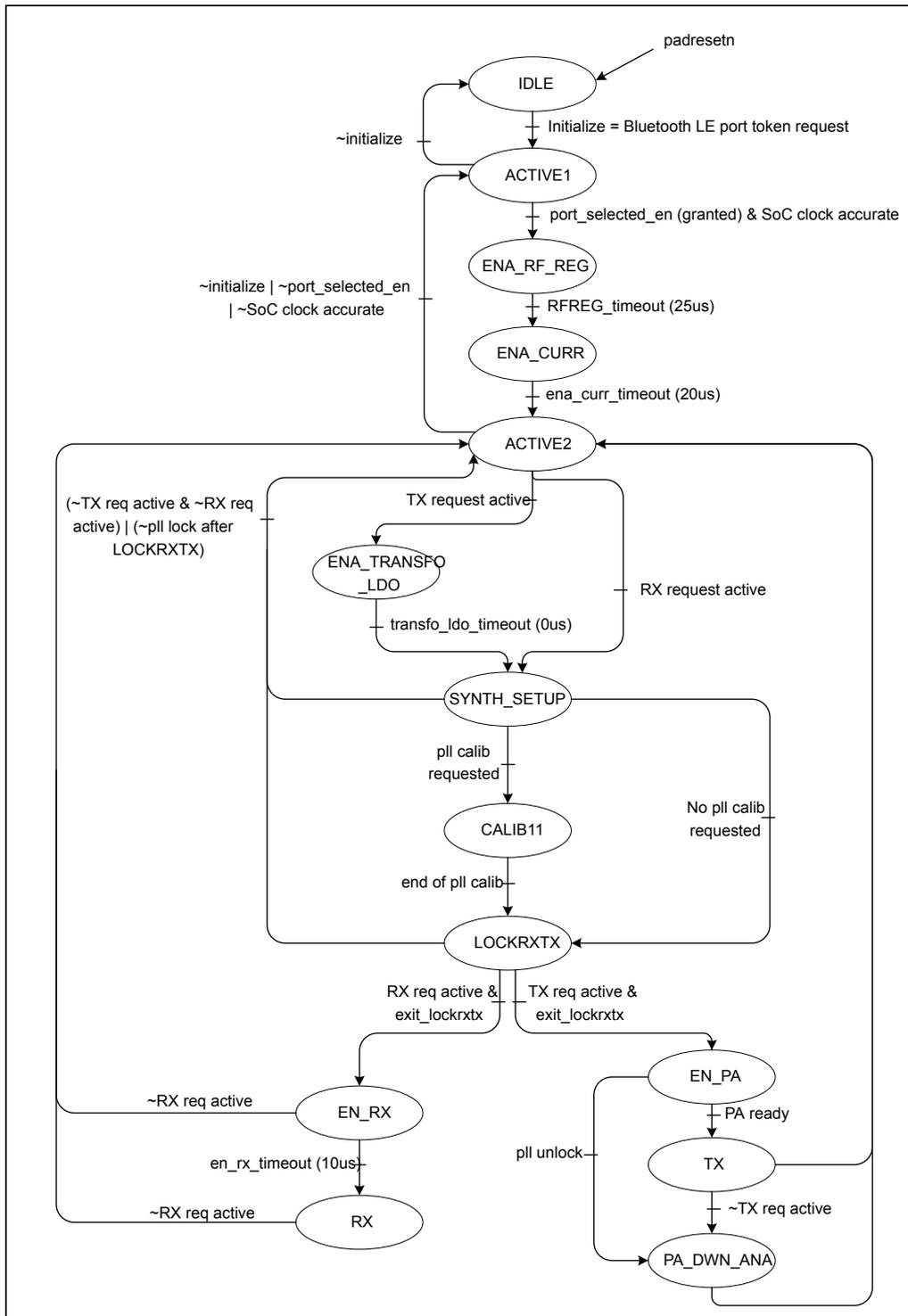
stateDiagram-v2
    [*] --> IDLE : padresetn
    IDLE --> ACTIVE1 : Initialize = Bluetooth LE port token request
    ACTIVE1 --> ENA_RF_REG : port_selected_en (granted) & SoC clock accurate
    ACTIVE1 --> IDLE : ~initialize
    ENA_RF_REG --> ENA_CURR : RFREG_timeout (25us)
    ENA_CURR --> ACTIVE2 : ena_curr_timeout (20us)
    ENA_CURR --> ACTIVE1 : ~initialize | ~port_selected_en | ~SoC clock accurate
    ACTIVE2 --> ENA_TRANSFO_LDO : TX request active
    ENA_TRANSFO_LDO --> SYNTH_SETUP : transfo_ldo_timeout (0us)
    ENA_TRANSFO_LDO --> ACTIVE2 : RX request active
    SYNTH_SETUP --> CALIB11 : pll calib requested
    CALIB11 --> LOCKRXTX : end of pll calib
    CALIB11 --> ACTIVE2 : No pll calib requested
    LOCKRXTX --> EN_RX : RX req active & exit_lockrxtx
    LOCKRXTX --> EN_PA : TX req active & exit_lockrxtx
    EN_RX --> RX : en_rx_timeout (10us)
    EN_RX --> ACTIVE2 : ~RX req active
    RX --> ACTIVE2 : ~RX req active
    EN_PA --> TX : PA ready
    TX --> PA_DWN_ANA : ~TX req active
    TX --> ACTIVE2 : pll unlock
    PA_DWN_ANA --> ACTIVE2
    ACTIVE2 --> ENA_TRANSFO_LDO : (~TX req active & ~RX req active) | (~pll lock after LOCKRXTX)
25.6.2 Radio FSM states overview
The table below lists, for each state, the exit condition and the duration in the state when there is a deterministic one.
Table 183. Radio FSM states summary (including exit conditions and timings)| Radio FSM state | State description | Condition to exit and duration in the state |
|---|---|---|
| IDLE | No RF activity requested: the analog RF IP is OFF | The Bluetooth® LE link layer requests a token to the RRM semaphore |
| ACTIVE1 | Wait for port granted and SoC accurate clock indication | Both hardware conditions are fulfilled |
| ENA_RF_REG | Enable the RF LDO | Timeout = 25 µs |
| ENA_CURR | Enable the reference current block inside the RF2G4 | Timeout = 20 µs |
| ACTIVE2 | This state confirms that all clock and power conditions are OK to accept an RF transfer request | Tx or Rx request occurrence |
| ENA_TRANSFO_LDO | Enable the LDO for the power amplifier | Timeout = 0 µs |
| SYNTH_SETUP | Start the RF PLL block | No timeout. Exit immediately (1 MR_BLE clock cycle duration) |
| CALIB11 | Start the PLL calibration block | End of calibration hardware information |
| LOCKRXTX (1) | Wait for RF PLL lock | Timeout = • 40 µs when no PLL calibration • 80 µs when PLL calibration |
| EN_RX | Enable the analog Rx chain | Timeout = 10 µs |
| Rx | Radio is in reception mode | End of Rx event (Rx timeout, Rx done...) |
| EN_PA (1) | Start the power ramp-up sequence (8 steps) up to targeted power on the antenna | Ready signal informing targeted Tx power is reached on the antenna (8 steps of 1.5 µs = 12 µs) |
| Tx | Radio is in transmission mode | End of Tx event (Tx done or skipped) |
| PA_DWN_ANA | Disable the power amplifier block | Timeout = 5 µs |
1. The radio FSM may abort the sequence and return to ACTIVE2 from those two states depending on RF PLL lock information:
- • LOCKRXTX: the decision occurs at the very end of the state to decide if the sequence should continue (PLL locked) or abort (PLL lock failed)
- • EN_PA: the decision to abort can occur at any time inside this state as soon as the RF PLL is no longer locked (PLL unlocked)
If the PLL unlock event occurs outside those two states, the radio FSM does not interfere. The SW is informed through an interrupt and is in charge of managing the situation.
The current state information is available in the FSM_STATUS_DIG_OUT radio register accessible by direct APB access (see Section 25.5.1: Radio register list ).
The radio FSM uses timeout to exit states linked to analog block settlement to guarantee a deterministic duration between ACTIVE2 and Tx or Rx state at any occurrence. This is mandatory to be able to fit with Bluetooth protocol timings requirements in a peer-to-peer communication flow.
Those deterministic durations are presented in the table below.
Table 184. ACTIVE2 to Tx or Rx state duration| Sequence | Duration | Comments |
|---|---|---|
| ACTIVE2 → Tx with RF PLL calibration | 92 µs | To be used when the Tx is done on a new frequency (channel) versus the previous RF transfer |
| ACTIVE2 → Tx without RF PLL calibration | 52 µs | To be used when the Tx is done on the same frequency (channel) as the previous RF transfer |
| ACTIVE2 → Rx with RF PLL calibration | 90 µs | To be used when the Rx is done on a new frequency (channel) versus the previous RF transfer |
| ACTIVE2 → Rx without RF PLL calibration | 50 µs | To be used when the Rx is done on the same frequency (channel) as the previous RF transfer |
25.6.3 Radio FSM interrupts
The Radio FSM provides a dedicated interrupt output signal to the system.
The Radio FSM generates 6 (2 are reserved) individually maskable interrupts grouped in an RfFsm_event[5:0] list:
- • RfFsm_event[0] = PLL Lock timeout
- – set when the counter to exit LOCKRXTX expires
- – whatever the lock status (PLL locked or not locked at timer expiration)
- • RfFsm_event[3] = PLL unlock detection
- – set when the PLL lock signal falls after the lock detection step.
- • RfFsm_event[4] = PLL lock failed
- – set if the PLL lock is not high when the Radio FSM exits the LOCKRXTX state
- – or set if the PLL is no more locked during EN_PA state or on exit of EN_PA state
- • RfFsm_event[5] = PLL calibration error
- – set if a PLL calibration error occurs during PLL calibration step.
- – Problems can concern the amplitude calibration and/or the frequency calibration and/or the KVCO calibration.
- – In this case, the detail can be read in SYNTH3_DIG_OUT[3:0] if SYNTHCAL0_DIG_ENG[3:0] = 0xC:
- ◦ SYNTHCAL3_DIG_OUT[3] = CAL_ERROR
- ◦ SYNTHCAL3_DIG_OUT[2] = CALAMP_ERROR
- ◦ SYNTHCAL3_DIG_OUT[1] = CALFREQ_ERROR
- ◦ SYNTHCAL3_DIG_OUT[0] = CALKVCO_ERROR
All the sources are combined into a single signal to be connected outside the IP_BLE to the interrupt controller of the SoC (see Table 115. Interruption summary for mapping in STM32WB05xZ).
The interrupts can be enabled/disabled individually through the radio controller APB registers:
- • Enable/disable through RADIO_CONTROL_IRQ_ENABLE register
- • Reading the RADIO_CONTROL_IRQ_STATUS register returns the interrupts status
- • Writing a '1' to the RADIO_CONTROL_IRQ_STATUS[x] clears the associated interrupt flag.
See Section 25.7.3: Radio controller registers for more details.
25.7 Radio controller
The radio controller is a small block in charge of two features:
- • Slow clock period measurement
- • Radio FSM interrupt management
25.7.1 Slow clock measurement
The radio controller contains a block dedicated to the slow clock measurement.
This measurement:
- • is launched automatically by the hardware when the system clock switches on accurate clock (external XO).
- • can be launched by the software when needed (by writing zero in CLK32K_PERIOD register)
The result provided by this block is both a period and a frequency information (in two separate results registers). The software can program the window of measurement (in slow clock cycle number) and the period result is provided in 16 MHz half-period unit.
25.7.2 Radio FSM interrupt management
During the sequences, the Radio FSM generates some interruptions to monitor some unexpected behavior at analog level. As the Radio FSM block does not have any APB interface, the interrupt control and status flags are managed inside the radio controller block through APB registers:
- • RADIO_CONTROL_IRQ_ENABLE register to enable the wanted interrupt sources.
- • RADIO_CONTROL_IRQ_STATUS register to get the status (on read) and to clear the interrupt (by writing '1' on the associated bit).
See Section 25.6.3: Radio FSM interrupts for more details on interrupt root causes.
25.7.3 Radio controller registers
25.7.3.1 Radio controller register list
The RADIO_CONTROL_BLOCKBaseAddress keyword used for all the register base address information corresponds to the Radio Controller registers base address decided by the SoC when integrating the IP.
Note: RADIO_CONTROL_BLOCKBaseAddress is 0x6000_1000 in the STM32WB05xZ product.
Table 185. Radio Controller registers list
| Address offset | Name | RW | Reset | Description |
|---|---|---|---|---|
| 0x00 | RADIO_CONTROL_ID | R | 0x00001000 | MR_BLE ID/version register |
| 0x04 | CLK32COUNT_REG | RW | 0x00000017 | Window length register |
| 0x08 | CLK32PERIOD_REG | R | 0x00000000 | Slow clock period register |
| 0x0C | CLK32FREQUENCY_REG | R | 0x00000000 | Slow clock frequency register |
| 0x10 | RADIO_CONTROL_IRQ_STATUS | RW | 0x00000000 | Radio controller interrupt status register |
| 0x14 | RADIO_CONTROL_IRQ_ENABLE | RW | 0x00000000 | Radio controller interrupt control register |
25.7.3.2 Radio controller registers
Table 186. RADIO_CONTROL_ID register description
| Bit | Field name | Reset | RW | Description |
|---|---|---|---|---|
| 31:16 | RESERVED31_16 | 0x0 | R | Reserved |
| 15:12 | PRODUCT | 0x02 | R | Incremented on major features add-on like new Bluetooth® LE SIG version support |
| 11:8 | VERSION | 0x1 | R | Cut number |
| 7:4 | REVISION | 0x0 | R | Incremented for metal fix version |
| 3:0 | RESERVED3_0 | 0x0 | R | Reserved |
Table 187. CLK32COUNT_REG register description
| Bit | Field name | Reset | RW | Description |
|---|---|---|---|---|
| 8:0 | SLOW_COUNT | 0x17 | RW | Program the window length (in slow clock period) for slow clock measurement. Note:
|
| 31:9 | RESERVED31_9 | 0x0 | R | Reserved |
| Bit | Field name | Reset | RW | Description |
|---|---|---|---|---|
| 18:0 | SLOW_PERIOD | 0x0 | RW | Indicates slow clock period information. The result provided in this field corresponds to the length of SLOW_COUNT periods of the slow clock (32 kHz) measured in 16 MHz half-period unit. Example: if SLOW_COUNT=0x17=23d and SLOW_PERIOD=24000d -> slow clock period = \( \text{SLOW\_PERIOD} / (16e6 \times 2 \times (\text{SLOW\_COUNT}+1)) \) = \( 24000 / (16e6 \times 2 \times 24) = 31.25e-6 \) A new calculation can be launched by writing zero in the CLK32PERIOD register. In this case, the time window uses the value programmed in the SLOW_COUNT field. |
| 31:19 | RESERVED31_19 | 0x0 | R | Reserved |
| Bit | Field name | Reset | RW | Description |
|---|---|---|---|---|
| 26:0 | SLOW_FREQUENCY | 0x0 | R | Value equal to \( (2^{39} / \text{SLOW\_PERIOD}) \) . |
| 31:27 | RESERVED31_27 | 0x0 | R | Reserved |
| Bit | Field name | Reset | RW | Description |
|---|---|---|---|---|
| 0 | SLOW_CLK_IRQ | 0x0 | RW | Slow clock measurement end of calculation interrupt status When read: - 0: no pending interrupt - 1: pending interrupt: slow clock period/frequency values are available. Write '1' to clear the interrupt. |
| 7:1 | RESERVED7_1 | 0x0 | R | Reserved |
| 13:8 | RADIO_FSM_IRQ | 0x0 | RW | Radio FSM interrupt status (aka RfFsm_event_irq). -0: no pending interrupt -1: pending interrupt RfFsm_event [5] = PLL calibration error RfFsm_event [4] = PLL lock failed RfFsm_event [3] = PLL unlock detection RfFsm_event [2] = reserved RfFsm_event [1] = reserved RfFsm_event [0] = lock_timeout Write '1' to clear the interrupt |
| 31:14 | RESERVED31_14 | 0x0 | R | Reserved |
| Bit | Field name | Reset | RW | Description |
|---|---|---|---|---|
| 0 | SLOW_CLK_IRQ_MASK | 0x0 | RW | Mask slow clock measurement interrupt 0: interrupt disabled 1: interrupt enabled |
| 7:1 | RESERVED7_1 | 0x0 | R | Reserved |
| 13:8 | RADIO_FSM_IRQ_MASK | 0x0 | RW | Mask for each RfFsm_event (Radio FSM) interrupt. - 0: Interrupt disabled - 1: Interrupt enabled. |
| 31:14 | RESERVED31_14 | 0x0 | R | Reserved |
25.8 IP_BLE
The Bluetooth LE link layer of the IP_BLE is a programmable automate which can act as a central or a peripheral.
The Bluetooth LE link layer embeds a Sequencer which automatically reads data and job request from link tables and link lists prepared in advance by the CPU in retention RAM. This allows the Bluetooth LE link layer to start a Bluetooth LE reception or transmission directly at low-power mode exit while the CPU is still booting and not yet able to manage any firmware action.
25.8.1 Overview
The IP_BLE embeds:
- • a Bluetooth Link layer
- • a modulator
- • a demodulator
The Bluetooth LE link layer manages:
- • the reception and transmission sequences including channel hopping,
- • on-the-fly encryption thanks to an embedded AES (which can also be used by the SW to compute LE privacy and manual encryption),
- • the antenna switching feature
The Bluetooth LE link layer embeds a Sequencer which uses information located in RAM tables to manage the RF transfer and part of the Bluetooth LE protocol. Those RAM tables need to be prepared by the SW.
In general, the process to generate a Bluetooth LE transfer is the following:
- • the CPU prepares some tables in RAM containing information about the next Bluetooth LE transfer(s)
- • the CPU programs one of the 3 possible timers that triggers/starts a sequence
- • When the selected timer matches the programmed value, the Sequencer starts to execute a Bluetooth LE sequence. This implies:
- – to read the RAM table to know what to do,
- – to (re-)program the radio register if needed,
- – to launch the Radio FSM with an Rx or Tx request depending on requested transfer.
- – once the analog RF is ready to transmit (respectively receive), to read the data payload from RAM (respectively to write the data payload in RAM)
- • Once the sequence is done (successfully or with errors), the Sequencer writes back in RAM updated information (flags, pointers, etc.)
Once RAM write-back is over, the Sequencer sends an interrupt to the CPU, related to interrupt mask programmed by the CPU (through the RAM table).
25.8.2 Bluetooth LE link layer Sequencer
The Sequencer needs a trigger event to start any action.
Then the Sequencer manages a transmission or reception (or no) sequence depending on the RAM table content it reads.
25.8.2.1 Possible trigger timers for the Sequencer
Three different timers can trigger a Bluetooth LE link layer sequence:
1. Wakeup timer event
- • this timer is inside the wakeup block and is the only one able to wake up the IP_BLE (and the SoC) from a low-power state
- • this timer is based on absolute time (slow clock granularity)
- • this timer is enabled by setting the BLUE_SLEEP_REQUEST_MODE[30] = BLE_WAKEUP_EN bit and the trigger event time is programmed in the BLUE_WAKEUP_TIME[31:0]
- • if an RRM command is enabled (through the StatMach table, RadioComListEna field), the sequencer requests the Command0 to the RRM-UDRA block during the sequence.
2. Timer1 timer
- • this timer is managed by the IP_BLE Sequencer itself but using the interpolated time
- • the granularity of this counter is 16 x slow clock period
- • this timer is enabled by setting timeout
- • the Timer1 trigs an event when the current interpolated time matches (or has gone past) the scheduled time programmed in the TIMEOUTREG APB register
- • this timer cannot be used in low-power mode
- • if an RRM command is enabled (through the StatMach table, RadioComListEna field), the Sequencer requests the Command1 to the RRM-UDRA block during the sequence.
3. Timer2 timer
- • this timer is based on a relative time and starts counting at the end of the previous transmission/reception
- • the granularity of this counter is 1 µs
- • this timer is a counter located inside the Sequencer of the Bluetooth LE link layer and cannot be used in low power mode
- • the Timer2 trigs an event when the counter matches the value programmed in the Timer2[19:0] bit field of the TxRxPack RAM table
- • this timer is enabled by setting the Timer2En bit in the TxRxPack RAM table of a sequence, allowing a trigger event for the next sequence (Tx/Rx sequence)
- • this timer is supposed to be used for short time delay between two Bluetooth transfers
- • if an RRM command is enabled (through the StatMach table, RadioComListEna field), the Sequencer requests the Command2 to the RRM-UDRA block during the sequence.
Ways to manage those 3 timers:
The 3 timers are managed (enabled/disabled) in a different way. The goal of the section below is to explain how to manage according to the use-case.
Each timer is one-shot. This means once it expires, it stops and the software has to reprogram/re-enable it for a new sequence.
Furthermore, as there is no mechanism to prevent more than one timer to be active at the same time, the software must ensure it does not start a timer while another one is already on-going for the next sequence.
Here is a summary of the enable/disable method for each timer:
- • the wakeup timer is enabled and programmed through the wakeup BLUE_WAKEUP_TIME APB register and has no interference with the two others so may be enabled in addition to Timer1 or Timer2.
- • the Timer1:
- – duration is programmed only through the IP_BLE TimeoutDestReg APB register
- – enable is done only through the IP_BLE TimeoutDestReg APB register
- – disable can be done through the IP_BLE TimeoutDestReg APB register
- – a hardware disable is automatically done by the Sequencer when it treats the Timer2 enable information in the TxRxPack RAM table under execution (whatever the TxRxPack.Timer2En bit value).
- • the Timer2:
- – can be programmed either through the IP_BLE TimeoutDestReg APB register or through the TxRxPack table
- – can be enabled/disabled either through the IP_BLE TimeoutDestReg APB register or through the TxRxPack table.
Note:
- • Programming respectively Timer1 or Timer2 through the IP_BLE TIMEOUTDESTREG APB register automatically disables respectively the Timer2 or Timer1.
- • If the Bluetooth LE sequence ends on a receive timeout (STATUSREG.RCVTIMEOUT = 1), Timer2 is not started even if the TxRxPack.Timer2En associated to this reception was 1.
- • Even if Timer2 can be enabled through the IP_BLE controller TIMEOUTDESTREG APB register, it is recommended not to do it in application flow and to use the RAM table.
- • TIMEOUTDESTREG[1:0] and TIMEOUTREG[31:0] need to be programmed at least 15 microseconds before the required start trigger.
25.8.2.2 Bluetooth LE sequence description
The Bluetooth LE sequence starts on the trigger event (from the wakeup timer or the Timer1 or the Timer2). The sequence is managed in three mains phases:
- • Initialization (split into 3 sub-steps)
- • reception or transmission
- • Context saving (to write back some updated field in RAM tables)
At the end of those phases, an interrupt (if at least one active source enabled) is generated to the CPU.
Note: the status flags and potential associated interrupt are set only at the end of the sequence and not in real time when the event that generates them occurs.
Note: the STATUSRREG.SEQDONE flag (and INTERRUPT1REG.SEQDONE if enabled in the GlobalStatMach table) is always raised when the Sequencer exits a sequence started by a trig event, whatever the process it followed (exit on error at any steps or run up to the end without problems). For this reason, this specific flag is not mentioned/repeated each time in this section.
The first RAM access done by the Sequencer on any trigger event is to get the GlobalStatMach word 0x01 to check the active bit to know if the parameters the Sequencer is about to read in the RAM table for the 1st INIT phase can be considered as ready and up to date.
If the active bit is low, the sequence stops, and the only actions done are:
- • setting NOACTIVEERROR flag in the STATUSREG IP_BLE APB register
- • and if IntNoActiveError is set in the GlobalStatMach, setting the NOACTIVEERROR in the INTERRUPT1REG IP_BLE APB register and generating an associated interrupt.
If the GlobalStatMach.Active bit is set, then the Sequencer starts the initialization phase.
Note: an automatic Active bit auto clear during context saving phase of the sequence can be enabled through the ChkFlagAutoClearEna bit in the GlobalStatMach. This avoids unexpected Tx/Rx due to Sequencer trigger event while the SW did not update the RAM tables (kind of SW acknowledge to allow the next transfer).
The figure below provides an overview of the Sequencer steps and control versus other blocks.
Figure 200. Sequencer steps overview
25.8.2.2.1 First initialization phase
During the first initialization phase, the Sequencer only reads the minimum information it needs in the RAM table to be able to start the Radio FSM for a reception or a transmission at the end of this phase.
The Sequencer launches up to 3 parallel tasks:
- 1. Set (or maintain if KeepSemaReq bit was set in the TxRxPack RAM table of the previous sequence) the take_req signal toward the RRM semaphore block to request/keep the token to access the radio resources.
- 2. If the RadioComListEna bit is set in the current StatMach table, send a command to the RRM UDRA:
- – Command 0 if trig event is the Wakeup timer
- – Command 1 if trig event is the Timer1
- – Command 2 if the trig event is the Timer2.
- 3. Get the minimum information needed to be able to start the Radio FSM (transmission or reception, channel number, PLL calibration requested or not, etc.).
At the end, this task also computes the channel number through the channel incrementer hardware block if requested and writes few radio registers (MOD_DEM_DIG_USR, RADIO_FSM_USR and PHYCTRL_DIG_USR) according to information from the RAM tables.
This first initialization step ends on a timeout defined by a bit field in the GlobalStatMach:
- • WakeupInitDelay (time unit is 16 x slow clock so typically 512 kHz) when trig event source is the wakeup timer
Note: despite the wakeup trigger event to start the sequence being based on a slow clock granularity, typ. 32 kHz (as the trigger occurs at BLUE_WAKEUP_TIME[31:4]), the Sequencer waits until the interpolate time is BLUE_WAKEUP_TIME[31:0] + WakeUpInitDelay to exit the 1 st INIT step which means the 512 kHz granularity is respected.
- • Timer12InitDelayCal (time unit is 1 µs) when the trig event is the Timer1 or when the trig event is the Timer2 and CalReq bit in TxRxPack table is set (PLL calibration requested)
- • Timer2InitDelayNoCal (time unit is 1 µs) when the trig event is the Timer2 and CalReq bit in the TxRxPack table is low (no PLL calibration requested).
InitDelay is used as a generic name for this duration to simplify the documentation as it can be 3 different bit fields that define it depending on the configuration.
Note: the main constraint on this delay depends on the previous setup:
- • If KeepSemaReq bit was set in the TxRxPack of the previous transfer, then the Radio FSM stays in ACTIVE2 and the main constraint to define the delay is the AHB accesses to read the RAM tables.
- • If KeepSemaReq bit was low in the TxRxPack of the previous transfer, then the RRM semaphore releases the token and Radio FSM goes back to IDLE. Then the main constraint for the delay is the duration for the Radio FSM to reach ACTIVE2 state from IDLE (25 µs for ENA_RF_REG step and 20 µs for ENA_CURR step).
- • In parallel, if accurate clock was turned off, there is also the delay to have accurate clock available to consider.
Caution: Whatever the trig event source, this InitDelay management in the Sequencer uses the system clock and the user must ensure the system runs an accurate clock to have a precise delay.
When the InitDelay timeout expires, the Sequencer checks several conditions to decide if it switches to the second initialization step or exits with error. The checked conditions are:
- • Radio FSM reached ACTIVE2 state meaning it is ready to receive a Tx or Rx request (and system clock is the accurate clock)
- • All RAM accesses and radio register writings to be done by the Sequencer during the first initialization step are over
- • No configuration error occurred (see Section 25.8.2.3.4: Configuration error for more details)
If all the conditions are true, then the Sequencer:
- • sends a Tx or Rx request to the Radio FSM depending on transfer direction indicated by TxMode bit in the current StatMach table
- • and switches to the second initialization step.
If at least one of the conditions is false then:
- • the sequence rises the flag(s) associated to the error(s). It can be:
- – STATUSREG.CONFIGERROR bit if a configuration error has been detected,
- – STATUSREG.ACTIVE2ERROR bit if the Radio FSM is not in ACTIVE2 at the end of the InitDelay ,
- – STATUSREG.SEMATIMEOUTERROR bit if the RRM semaphore did not grant the IP_BLE on time,
- • No RAM write back action is done.
- • The error bits set in the STATUSREG register also appear in INTERRUPT1REG if their associated interrupt enable bit is set in the GlobalStatMach table.
25.8.2.2.2 Second initialization step
The 2 nd INIT step is used by the Sequencer to get all the information from the RAM tables linked to the RF transfer to proceed (except DataPtr and TxDataReady bit fields).
This means the software must have filled all the RAM table information (except DataPtr and TxDataReady bit fields) when the InitDelay timeout expires.
The 2 nd INIT step starts when the Tx or Rx request is sent to the Radio FSM. The first action of the Sequencer is to read few delays in the GlobalStatMach. Those delays are needed during the 2 nd INIT and DATA INIT steps.
This 2 nd INIT step ends on a timeout based on 2 pieces of information read in the GlobalStatMach:
- 1. init_radio_delay (in µs), used as a generic name for this duration to simplify the documentation: it is one possibility out of 4 different bit fields depending on the transfer configuration:
- – TransmitNoCalDelayChk when the transfer is a Tx and no PLL calibration is requested (CalReq bit is low),
- – TransmitCalDelayChk when the transfer is a Tx and a PLL calibration is requested (CalReq bit is set),
- – ReceiveNoCalDelayChk when the transfer is an Rx and no PLL calibration is requested (CalReq bit is low),
- – ReceiveCalDelayChk when the transfer is an Rx and a PLL calibration is requested (CalReq bit is set).
- 2. TxdataReadyCheck: duration given to the Sequencer to get the two last pieces of information, which are DataPtr and TxDataReady information in the RAM table. This last reading is done in the third initialization step called DATA_INIT.
The 2 nd INIT ends after “init_radio_delay – TxdataReadyCheck” µs.
From the 2 nd INIT step, the Radio FSM is running in parallel to the Sequencer getting information in the RAM tables. The user must ensure the init_radio_delay duration does not exceed the RF analog setup time up to powering on the antenna for a transmission (or ready to receive on the antenna). This means the 2 nd INIT step must not exceed:
- • the duration of the Radio FSM to go from ACTIVE2 to Tx state for a transmission with few µs of margin
- • the duration of the Radio FSM to go from ACTIVE2 to Rx state for a reception.
- Note:
- • For transmission, the init_radio_delay timeout must expire before the Radio FSM is in Tx mode to avoid missing the start of the preamble sending on the antenna (otherwise garbage is sent while the preamble is supposed to be output).
- • For a reception, the init_radio_delay must expire close to the switch in Rx state of the Radio FSM, knowing the RcvTimeout counter starts when the init_radio_delay expires.
At the very beginning of the 2 nd INIT step:
- • the Sequencer starts an internal relative timer
- • In parallel, the Sequencer reads the init_radio_delay, ConfigEndDuration and TxdataReadyCheck information in the GlobalStatMach.
The 2 nd INIT step really starts to fetch information related to the transfer in the RAM tables when the relative timer reaches “init_radio_delay – ConfigEndDuration”.
The GlobalStatMach.ConfigEndDuration bit field allows delaying the reading of the transfer information contained in the RAM tables by the Sequencer. The goal of this delay is to provide more margin to the SW to fill the RAM table information that is read during 2 nd INIT. This is possible as the RAM table read session is shorter than the analog radio setup duration. The figure below provides a summary of the timing information contributors for the initialization steps.
Figure 201. Sequencer Initialization steps timings overview
25.8.2.2.3 Data initialization step
This data INIT step starts when the 2 nd INIT step ends.
During this step, the Sequencer only gets 2 values from the table:
- • TxDataReady bit in the TxRxPack indicating enough bytes are present in the Tx payload data buffer (in case of transmission only).
- • DataPtr bit field in the TxRxPack.
The GlobalStatMach.TxdataReadyCheck is used to delay the start of this DATA INIT step to allow more time to the software to provide the data pointer (and first values to transmit if transfer is a transmission).
The DATA INIT step ends when the relative timer (started at the beginning of the 2nd INIT step) reaches init_radio_delay:
- • if all conditions are OK (AllTableReady read at 1, TxDataReady read at 1 for a transmission, Radio FSM still in a state between ACTIVE2 and Rx or Tx, command_end received from the RRM if a UDRA command was launched in parallel, a start pulse is sent to the receive/transmit block for a reception/transmission).
- • or else no start pulse is sent to the receive/transmit block and status/interrupt flags are updated in the Bluetooth® LE APB registers (no RAM write-back is done).
For transmission, a synchronization mechanism is in place between the transmit block and the Radio FSM: the transmit block waits for the Tx state information from the Radio FSM to know when data can be sent to the modulator. As the transmit block is supposed to receive the start pulse from the Sequencer a bit before the Radio FSM reaches the Tx state, a wait window needs to be defined to avoid waiting forever: this time window is defined in the GlobalStatMach.TxReadyTimeout bit field.
Caution: It is the responsibility of the software to ensure that the init_radio_delay, the ConfigEndDuration and the TxdataReadyCheck values are coherent to guarantee both data ready on time in the table and start pulse sent on time to the receive/transmit block.
25.8.2.2.4 Transmission/reception step
The transmission/reception step starts when the start pulse is sent by the Sequencer to the transmit or to the receive block.
This step ends when the transmit/receive block indicates that the transfer is done:
- • all data transmitted for a transmission (followed by a waiting time defined by GlobalStatMach.TxdelayEnd)
- • a frame has been received or the programmed timeout to wait for a reception expired without any reception.
Important:
- • When a transmission is completed, the timer2, if it is programmed, starts counting only when GlobalStatMach.TxdelayEnd has elapsed
- • When a reception is completed, if the exit reason is a timeout, the timer2 does not start.
25.8.2.2.5 Context saving step
The context saving steps consist of RAM write-back operation in some RAM table words to update with the result of the RF transfer that just ended.
This step starts when the Sequencer obtains the transfer done information from the transmit or receive block.
The RAM write-back impacts the following RAM table elements:
- • GlobalStatMach Word1 if the GlobalStatMach.ChkFlagAutoClearEna bit is set:
- – clear the Active bit
- – write back the rest of the bit field of this Word1 with the value previously read by the Sequencer in the RAM table.
- • StatMach Word0: update SN, NESN, remapped channel, and next transfer direction (TxMode)
- • StatMach Word1: update the TxPoint[31:0] with TxPointNext[31:0] or keep the same.
- • StatMach Word2: update the RcvPoint[31:0] with RcvPointNext[31:0] or keep the same.
- • StatMach Word3: update the TxPointPrev[31:0] with TxPoint[31:0] or keep the same.
- • StatMach Word4: update the RcvPointPrev[31:0] with RcvPoint[31:0] or keep the same.
- • StatMach Word5: update the TxPointNext[31:0] or keep the same.
- • StatMach Word6: update the PCntTx[31:0] or keep the same.
- • StatMach Word7: update the PCntTx[39:32] and PCntRcv[23:16] or keep the same.
- • StatMach Word8:
- – update the PCntRcv[39:24] or keep the same
- – the rest of the Word8 is written back with value previously read by the Sequencer in the RAM table.
Note: See Section 25.8.5.1: Pointers management and packet counter for pointer management details .
25.8.2.2.6 Bluetooth® LE sequence summary
The sequences of operations characterizing a transmission and a reception are summarized in the following timing diagrams.
Figure 202. Tx sequence
The diagram illustrates the timing sequence for a transmission (Tx). It starts with a 'Trigger event' leading into a '1 st INIT' phase, followed by a delay 'InitDelay'. This is followed by a '2 nd INIT' phase. A 'ConfigEnd Duration' is marked between the end of the 2 nd INIT and the start of 'DATA INIT'. From the start of 'DATA INIT', a 'TxData ReadyChk' timer starts. A 'TxReady Timeout' is shown as a duration starting from the end of 'DATA INIT'. The 'init_radio_delay' is indicated as the time from the start of '2 nd INIT' to the start of 'TxDelay Start'. The sequence then enters the 'TX' phase, which includes 'TxDelay Start' and 'TxDelay End'. Finally, a 'RAM write back' operation occurs, followed by an 'IRQ to CPU' signal.
Figure 203. Rx sequence
25.8.2.3 Possible root causes of aborted sequence
It may happen that the sequence is not started or interrupted before the end for different reasons.
In any case, the SeqDone flag (and interrupt if enabled) occurs at the end of a sequence whatever the status (successful or failed).
Then, some status/error flags (with associated maskable interrupt) are available to obtain the reason of the abortion or to have complementary information on the sequence that just occurred.
25.8.2.3.1 Active bit is low
The sequence is stopped just after the trigger event because the Active bit in the GlobalStatMach RAM table is read equal to 0.
If active bit is low, then:
- • no sequence is started (Radio FSM and transmit/receive blocks not informed),
- • no timer management is done (no update / reprogramming of the different timers is done),
- • no RAM write-back occurs, RAM tables are left unchanged,
- • the NOACTIVEERROR bit is set in the STATUSREG IP_BLE APB register,
- • if the NOACTIVEERROR bit in the GlobalStatMach word 0x05 is set, the NOACTIVEERROR bit is set in the INTERRUPT1REG IP_BLE APB registers and a Bluetooth® LE interrupt is generated to the CPU
- – The enable mask is readable in INTERRUPT1ENABLEREG.NOACTIVEERROR bit.
25.8.2.3.2 RRM semaphore does not grant the IP_BLE on time
On a trigger event and if active bit is high, the Sequencer requests the token to the RRM semaphore to have control of the radio resources.
If, at the end of the initialization delay (WakeupInitDelay or Timer12InitDelayCal or Timer2InitDelayNoCal), the RRM still does not confirm the IP_BLE has been granted, then:
- • no sequence is started (Radio FSM and transmit/receive blocks not informed)
- • no timer management is done (no update/reprogramming of the different timers is done)
- • no RAM write-back occurs, RAM tables are left unchanged,
- • the SEMATIMEOUTERROR bit is set in the STATUSREG IP_BLE APB register
- • if the IntSemaTimeoutError bit in the GlobalStatMach word 0x05 is set, the SEMATIMEOUTERROR bit is set in the INTERRUPT1REG IP_BLE APB registers and an interrupt is generated to the CPU
- – The enable mask is readable in INTERRUPT1ENABLEREG.SEMATIMEOUTERROR bit.
25.8.2.3.3 Radio FSM not in ACTIVE2 state on time
This error happens if the Radio FSM is not in ACTIVE2 state at the end of the 1 st INIT step (on InitDelay timeout expiration).
If, at the end of the initialization delay (WakeupInitDelay or Timer12InitDelayCal or Timer2InitDelayNoCal), the Radio FSM has still not confirmed it is ready to start a Tx or Rx sequence (no accurate clock present for instance):
- • no sequence is started (Radio FSM and transmit/receive blocks not informed)
- • no timer management is done (no update/reprogramming of the different timers is done)
- • no RAM write-back occurs, RAM tables are left unchanged
- • the ACTIVE2ERROR bit is set in the STATUSREG IP_BLE APB register
- • if the IntActive2Error bit in the GlobalStatMach word 0x05 is set, the Active2Error bit is set in the INTERRUPT1REG Bluetooth® LE APB registers and a IP_BLE interrupt is generated to the CPU
- – The enable mask is readable in INTERRUPT1ENABLEREG.ACTIVE2ERROR bit.
25.8.2.3.4 Configuration error
A configuration error occurs if the value contained by the Rcvpoint or Txpoint field or IQSamplingPtr of the current StatMach RAM table is not modulo 4 (does not correspond to a 32-bit aligned address).
Note: the StatMach.IQSamplingPtr value is checked only for some values in other RAM table bit fields. Refer to Section 25.8.6.4.4: IQSamplesPtr[31:0] or AntennaPatternPtr[31:0] not 32-bit aligned for details .
In this case:
- • the Sequencer stops the sequence at the end of the 1 st initialization phase (so neither the Radio FSM nor the transmit/receive blocks received any request),
- • no timer management is done (no update/reprogramming of the different timers)
- • no RAM write-back occurs
- • the STATUSREG.CONFIGERROR bit is set
- • if the IntConfigError bit in the GlobalStatMach RAM table is set, the INTERRUPT1REG.CONFIGERROR is set and an IP_BLE interrupt is generated
- – The enable mask is readable in INTERRUPT1ENABLEREG.CONFIGERROR bit.
25.8.2.3.5 Address pointer error
An address pointer error occurs if the TxRxPack.NextPtr[31:24], the TxRxPack.DataPtr[31:24] or the StatMach.IQSamplestPtr[31:24] (if TxRxPack.CTEAndSamplingEnable=1) is not equal to the SoC RAM base address.
In this case:
- • no transmission or reception is started
- • the Tx or Rx request towards Radio FSM is canceled
- • no RAM write-back is done
- • the STATUSREG.ADDPOINTERROR bit is high at the end of the sequence
- • if the IntAddPointError bit in the GlobalStatMach is high, the INTERRUPT1REG.ADDPOINTERROR bit is set and an IP_BLE interrupt is generated.
- – The enable mask is readable in INTERRUPT1ENABLEREG.ADDPOINTERROR bit.
25.8.2.3.6 PLL lock fail (only if GlobalStatMach.AutoTxRxSkipEn = 1)
If the AutoTxRxSkipEn bit in the GlobalStatMach RAM table is set, the Sequencer skips the sequence if the PLL lock fail information is raised.
This PLL lock fail corresponds to the fact that the PLL did not lock on time and is provided by the Radio FSM. It is checked by the Sequencer at the end of the initialization step, before entering the Tx-Rx step.
In this case:
- • no transmission or reception is started
- • the Tx or Rx request towards Radio FSM is canceled
- • no RAM write-back is done
- • the STATUSREG.TXRXSKIP bit is high at the end of the sequence
- • if the IntTxRxSkip bit in the GlobalStatMach is high, the INTERRUPT1REG.TXRXSKIP bit is set and a Bluetooth® LE interrupt is generated
- – The enable mask is readable in INTERRUPT1ENABLEREG.TXRXSKIP bit.
25.8.2.3.7 TxRxSkip APB command
An APB command is available to skip an on-going Tx or Rx transfer. The software needs to write '1' in the TXRXSKIP bit of the CMDREG IP_BLE APB register.
Note: This bit is auto-cleared immediately by the hardware.
The software must be aware that the TxRxSkip APB command is considered only during a sequence. Otherwise the skip request is ignored (not recorded and no TxRxSkip interrupt/status flag is raised on the next sequence).
The behavior differs depending on the TxRxSkip command that occurs inside the sequence.
Table 192. Summary of flags and RAM table pointers behavior versus Tx Skip command
| “Skip at” phase | Interrupt flags | RAM table pointers updated | RAM write-back | ||||
|---|---|---|---|---|---|---|---|
| DONE bit[25] | TXRXSKIP Bit[21] | TXERROR_1 Bit[9] | Tx Prev | Tx | Tx next | ||
| 1 st INIT | NO | YES | NO | NO | NO | NO | NO |
| 2 nd INIT | NO | YES | NO | NO | NO | NO | NO |
| DATA INIT | NO | YES | NO | NO | NO | NO | NO |
| Tx | YES | YES | YES | NO | NO | YES | YES |
| CONTECT SAVING | YES | NO | NO | YES | YES | YES | YES |
Table 193. Summary of flags and RAM table pointers behavior versus Rx Skip command
| “Skip at” phase | Interrupt flags | RAM table Pointers updated | RAM write-back | ||||
|---|---|---|---|---|---|---|---|
| RCVOK Bit[31] | RCVRCERR Bit[30] | DONE Bit[25] | TXRXSKIP Bit[21] | RCV Prev | RCV | ||
| 1 st INIT | NO | NO | NO | YES | NO | NO | NO |
| 2 nd INIT | NO | NO | NO | YES | NO | NO | NO |
| DATA INIT | NO | NO | NO | YES | NO | NO | NO |
| Rx | NO | YES | YES | YES | NO | YES | YES |
| CONTECT SAVING | YES | NO | YES | NO | YES | YES | YES |
In all scenarios, the IntTxRxSkip bit in the GlobalStatMach must be high to have an interrupt generated when the STATUSREG.TXRXSKIP bit is high. In this case, the INTERRUPT1REG.TXRXSKIP bit is also high. The enable mask is readable in INTERRUPT1ENABLEREG.TXRXSKIP bit.
25.8.2.3.8 AllTableReady bit not set on time
This error is linked to:
- • Interrupt mask in GlobalStatMach.IntAllTableReady.
- – This mask is readable in INTERRUPT1ENABLEREG.ALLTABLEREADYERROR bit.
- • Status flag in ALLTABLEREADYERROR bit.
- • Interrupt flag in INTERRUPT1REG.ALLTABLEREADYERROR bit.
During the 2 nd INIT step, the TxRxPack.AllTableReady bit is read by the Sequencer just after the ConfigEndDuration waiting loop (but checks its value only when exiting DATA INIT step at the end of init_radio_delay).
The role of this bit is to guarantee the information related to the transmission/reception packet (especially data pointers) in the TxRxPack (except the payload bytes when transmission) are valid/up-to-date.
If the recorded TxRxPack.AllTableReady is not high:
- • no transmission or reception is started
- • Tx or Rx request towards Radio FSM is canceled
- • no RAM write-back is done
- • the STATUSREG.ALLTABLEREADYERROR bit is high at the end of the sequence
- • if the IntAllTableReadyError bit in the GlobalStatMach is high, the INTERRUPT1REG.ALLTABLEREADYERROR bit is set and an IP_BLE interrupt is generated
- – The enable mask is readable in INTERRUPT1ENABLEREG.ALLTABLEREADYERROR bit.
25.8.2.3.9 TxdataReady bits not set on time
This bit is used only when the on-going transfer is a transmission (not checked on a reception).
It adds flexibility to the software to be able to go on filling the data payload to transmit while the transmission has already started on the antenna.
The recommendation is to set this bit only after at least 16 bytes of Tx data payload are available in the data buffer.
The Sequencer reads the TxRxPack.TxDataReady bit at the beginning of the DATA INIT step but checks its value only at the end of the init_radio_delay.
If the recorded TxRxPack.TxDataReady is not high:
- • no transmission is started
- • Tx request towards Radio FSM is canceled
- • no RAM write-back is done
- • the STATUSREG.TXDATAREADYERROR bit is high at the end of the sequence
- • if the IntTxDataReadyError bit in the GlobalStatMach is high, the INTERRUPT1REG.TXDATAREADYERROR bit is set and an IP_BLE interrupt is generated
- – The enable mask is readable in INTERRUPT1ENABLEREG.TXDATAREADYERROR bit.
25.8.2.3.10 Receive length error
This aborting issue can occur only on reception.
A receive length error is detected if the received length value decoded in the received frame header is greater than the StatMach.MaxReceivedLength[7:0] bit field. This feature can be used when free RAM area is limited and does not allow receiving large packets.
If the receive block detects a packet length in the received header that is greater than the StatMach.MaxReceiveLength value:
- • the receiver treats only MaxReceiveLength bytes of data and stops its sequence
- – any extra bytes sent by the demodulator are ignored
- • the data payload written back in RAM is limited to MaxReceiveLength + 2 bytes (corresponding to header + length) + potential CTEINFO byte in case of data PDU channel with CTE present
- • the Sequencer manages the reception step as usual as the receive block provides a done pulse, it receives a receive done pulse from the receive block
- – this leads to stopping the Radio FSM receive mode while data are potentially still arriving on the antenna
- • a RAM write-back occurs
- • the STATUSREG.RCVLENGTHERROR bit is high at the end of the sequence
- • if the IntRcvLengthError bit in the GlobalStatMach is high, the INTERRUPT1REG.RCVLENGTHERROR bit is set and an IP_BLE interrupt is generated
- – The enable mask is readable in INTERRUPT1ENABLEREG.RCVLENGTHERROR bit.
Note: As the receiver truncates the received frame to a reduced length, a CRC error occurs in parallel and potential other side effect error flags. So, the RCVLENGTHERROR flag must be considered before the others regarding a reception.
25.8.3 IP_BLE interrupts
The Bluetooth® LE link layer provides 2 separate interrupt lines:
- • int1: Bluetooth® LE sequence interrupt (linked to sequence that just occurred)
- • int2: AES interrupt (manual or LE privacy end of calculation)
The IP_BLE interrupts:
- • the IP_BLE interrupts are enabled through the RAM tables (some in the GlobalStatMach, others in TxRxPack)
- • a copy of the applied enable mask is available in the INTERRUPT1ENABLEREG IP_BLE APB register
- • the IP_BLE interrupts status can be read when an interrupt triggers at CPU level and is available in the INTERRUPT1REG Bluetooth® LE APB register
- • the IP_BLE interrupts are cleared by writing '1' in the associated bit in the INTERRUPT1REG Bluetooth® LE APB register
- • a dedicated internal timer is started when the interrupt is raised: its value is accessible in the INTERRUPT1LATENCYREG register. The goal of this register is to inform the interrupt handler SW about how long the interrupt is pending. This latency window is limited to 255 µs. Over this delay, the read value stays at 255.
Note: only enabled interrupts can be read at '1' in this INTERRUPT1REG register. To have the equivalent without enable mask, the STATUSREG IP_BLE APB register must be read.
The AES interrupts:
- • the AES interrupts are enabled through IP_BLE APB registers (MANAESCMDREG for manual AES and AESLEPRIVCMDREG for LE privacy AES)
- • the AES interrupts status can be read in the INTERRUPT2REG IP_BLE APB register and represents/means "end of calculation" information
- • the AES interrupts are cleared by writing '1' in the associated bit in the INTERRUPT2REG IP_BLE APB register.
Note: the "end of calculation" information is only available through enabled interruption. The MANAESSTATREG and the AESLEPRIVSTATREG IP_BLE APB registers contain other flags, not equivalent to INTERRUPT2REG registers.
25.8.4 IP_BLE RAM tables
Each time a trigger event is sent to the Bluetooth® LE link layer, the Sequencer fetches the RAM tables in RAM to get the needed information to know what to configure for the radio and which sequence to start (Rx or Tx).
There are several types of table:
- • The GlobalStatMach: this table is unique.
- • The StatMach: one table by active connection (up to 128 supported by the hardware).
- • The TxRxPack: one table packet in Rx or in Tx. So, there is no predefined number of those tables. They are used as a link list from one packet to another during a full connection.
- • The DataPack table corresponding to the data buffers pointed by the DataPtr in the TxRxPack. It contains the PDU section of the Bluetooth packet.
Figure 204. RAM table dependency overview gives an overview of RAM tables dependencies. In the provided example, the GlobalStatMach is currently managing the connection number X (StatMachx on-use) and the data buffer points to itself from the third transfer of each type.
Figure 204. RAM table dependency overview
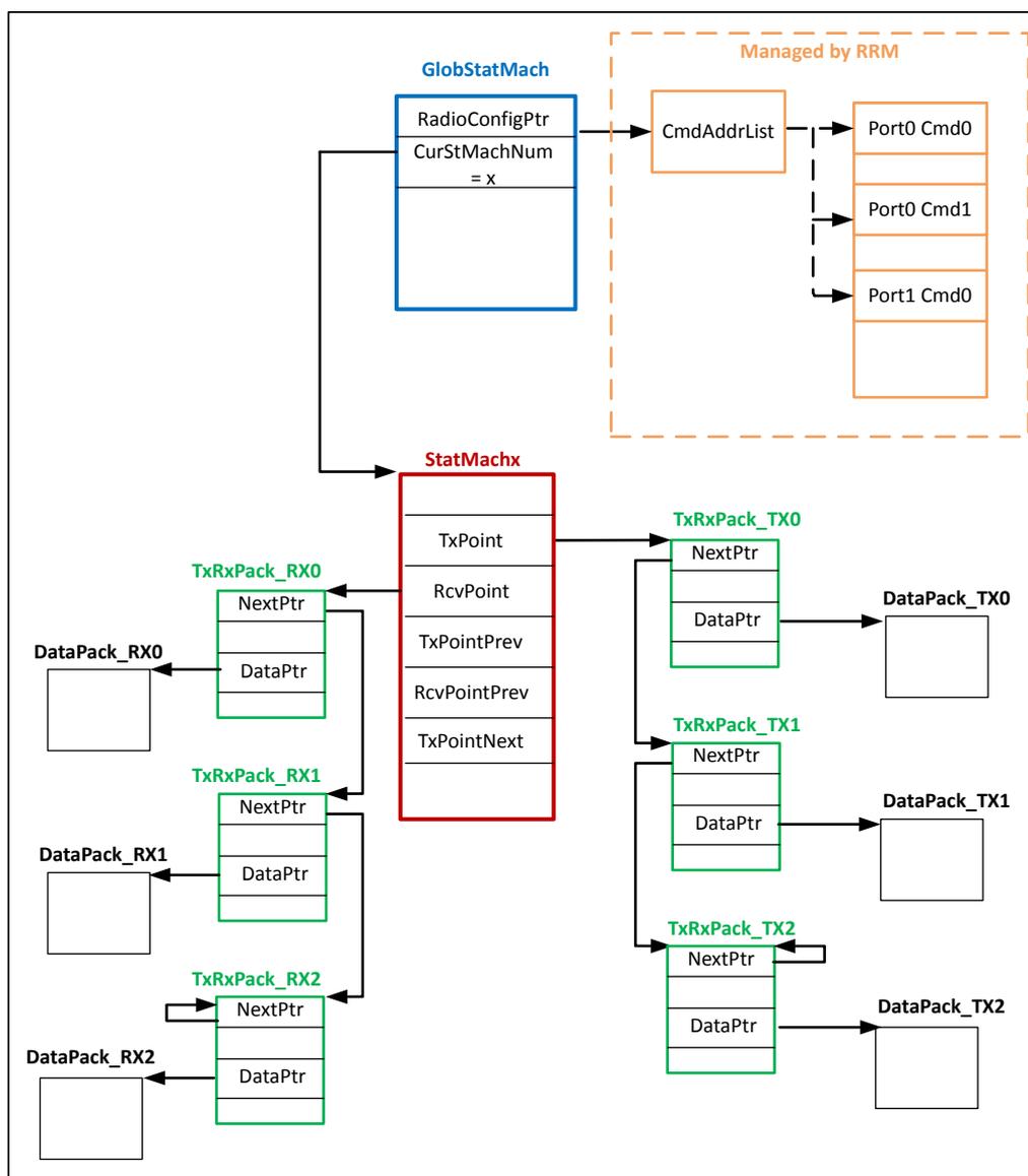
The diagram illustrates the RAM table dependency overview for the Radio IP. It shows the following structures and their dependencies:
- GlobStatMach
(Blue box):
- Fields:
RadioConfigPtr,CurStMachNum = x. RadioConfigPtrpoints to CmdAddrList .- CmdAddrList (Orange box, Managed by RRM ) points to Port0 Cmd0 , Port0 Cmd1 , and Port1 Cmd0 .
CurStMachNumpoints to StatMachx .
- Fields:
- StatMachx
(Red box):
- Fields:
TxPoint,RcvPoint,TxPointPrev,RcvPointPrev,TxPointNext. TxPointpoints to TxRxPack_TX0 .RcvPointpoints to TxRxPack_RX0 .TxPointPrevpoints to TxRxPack_TX1 .RcvPointPrevpoints to TxRxPack_RX1 .TxPointNextpoints to TxRxPack_TX2 .
- Fields:
- TxRxPack_RX0
(Green box):
- Fields:
NextPtr,DataPtr. NextPtrpoints to DataPack_RX0 .DataPtrpoints to TxRxPack_RX1 .
- Fields:
- TxRxPack_RX1
(Green box):
- Fields:
NextPtr,DataPtr. NextPtrpoints to DataPack_RX1 .DataPtrpoints to TxRxPack_RX2 .
- Fields:
- TxRxPack_RX2
(Green box):
- Fields:
NextPtr,DataPtr. NextPtrpoints to DataPack_RX2 .DataPtrpoints to TxRxPack_RX0 (forming a loop).
- Fields:
- TxRxPack_TX0
(Green box):
- Fields:
NextPtr,DataPtr. NextPtrpoints to DataPack_TX0 .DataPtrpoints to TxRxPack_TX1 .
- Fields:
- TxRxPack_TX1
(Green box):
- Fields:
NextPtr,DataPtr. NextPtrpoints to DataPack_TX1 .DataPtrpoints to TxRxPack_TX2 .
- Fields:
- TxRxPack_TX2
(Green box):
- Fields:
NextPtr,DataPtr. NextPtrpoints to DataPack_TX2 .DataPtrpoints to TxRxPack_TX0 (forming a loop).
- Fields:
25.8.4.1 GlobalStatMach RAM table
The GlobalStatMach location is frozen by hardware at address 0x2000_00C0 in the STM32WB05xZ.
25.8.4.1.1 GlobalStatMach RAM table overview
The GlobalStatMach is unique and mainly contains static information/options.
Table 194. GlobalStatMach RAM table
| Word | Byte addr | R/W by Bluetooth LE | 7 | 6 | 5 | 4 | 3 | 2 | 1 | 0 |
|---|---|---|---|---|---|---|---|---|---|---|
| 0x00 | 0x0 | No | RadioConfigPtr[7:0] | |||||||
| 0x1 | RadioConfigPtr[15:8] | |||||||||
| 0x2 | RadioConfigPtr[23:16] | |||||||||
| 0x3 | RadioConfigPtr[31:24] | |||||||||
| 0x01 | 0x4 | R/W | Active | CurStMachNum | ||||||
| 0x5 | WakeupInitDelay | |||||||||
| 0x6 | Timer12InitDelayCal | |||||||||
| 0x7 | Timer2InitDelayNoCal | |||||||||
| 0x02 | 0x8 | R | TransmitCalDelayChk | |||||||
| 0x9 | TransmitNoCalDelayChk | |||||||||
| 0xA | ReceiveCalDelayChk | |||||||||
| 0xB | ReceiveNoCalDelayChk | |||||||||
| 0x03 | 0xC | R | ConfigEndDuration | |||||||
| 0xD | TxdataReadyCheck | |||||||||
| 0xE | TxdelayStart | |||||||||
| 0xF | TimeCapture | TimeCaptureSel | TxdelayEnd | |||||||
| 0x04 | 0x10 | R | TxReadyTimeout | |||||||
| 0x11 | RcvTimeout[7:0] | |||||||||
| 0x12 | RcvTimeout [15:8] | |||||||||
| 0x13 | RcvTimeout [19:16] | |||||||||
| 0x05 | 0x14 | R | ChkFlagAutoClearEna | AutoTxRxskipEn | ||||||
| 0x15 | ||||||||||
| 0x16 | IntNoActiveLError | IntTxDataReadyError | IntAllTableReadyError | IntAddPointError | ||||||
| 0x17 | IntConfigError | IntActive2Err | intTxRxSkip | IntSeqDone | IntSemaTimeoutError | IntRcvLengthError | ||||
| 0x06 | 0x18 | R | DefaultAntennalD[6:0] | |||||||

| Word | Byte addr | R/W by Bluetooth LE | 7 | 6 | 5 | 4 | 3 | 2 | 1 | 0 |
|---|---|---|---|---|---|---|---|---|---|---|
| 0x06 | 0x19 | R | ||||||||
| 0x1A | ||||||||||
| 0x1B |
- Note:
- • grey cells are unused cells
- • pink cells are related to debug/qualification topic.
The following section describes the GlobalStatMach bit fields to help the user to program accurately the table.
- Note: init_radio_delay is the generic name for the delay that can be TransmitCalDelayChk or TransmitNoCalDelayChk or ReceiveCalDelayChk or ReceiveNoCalDelayChk depending on transfer configuration (see Section 25.8.2.2.2: Second initialization step for more details).
25.8.4.1.2 GlobalStatMach RAM table registers list
Table 195. GlobalStatMach RAM table register list
| Address offset | Name | RW | Reset | Description |
|---|---|---|---|---|
| 0x00 | WORD0 | RW | 0x00000000 | Word0 register |
| 0x04 | WORD1 | RW | 0x00000000 | Word1 register |
| 0x08 | WORD2 | RW | 0x00000000 | Word2 register |
| 0x0C | WORD3 | RW | 0x00000000 | Word3 register |
| 0x10 | WORD4 | RW | 0x00000000 | Word4 register |
| 0x14 | WORD5 | RW | 0x00000000 | Word5 register |
| 0x18 | WORD6 | RW | 0x00000000 | Word6 register |
Table 196. GlobalStatMach.WORD0 register description
| Bit | Field name | Reset | RW | Description |
|---|---|---|---|---|
| 31:0 | RADIOCONFIGPTR | 0x00000000 | RW | Radio Configuration address Pointer. Contains the address of the command_start_list used by the RRM block to execute UDRA command. Caution: This pointer must be 32-bit aligned. Note: This value is loaded automatically by the RRM when the MR_BLE exits reset. However, it is also possible to make the RRM reload it through a reload command in the UDRA_CTRL register. |
Table 197. GlobalStatMach.WORD1 register description
| Bit | Field name | Reset | RW | Description |
|---|---|---|---|---|
| 6:0 | CURSTMACHNUM | 0x0 | RW | Current connection machine number. Defines the state machine number (in the range from 0 to 127) which is running for the current transmission or reception. It is used to calculate the RAM address from which the State machine table ("StateMach") is read. Note: This field is written back with value read at the beginning of the sequencer only if the ChkFlagAutoClearEna bit = '1'. |
| 7 | ACTIVE | 0x0 | RW | Must be at '1' when the trig event (Wakeup Timer, Timer1 or Timer2) occurs to start Bluetooth® LE link layer sequence. Otherwise, no RF sequence nor timer management is done by the Sequencer. Note: This field is written back to '0' only if the ChkFlagAutoClearEna bit = '1'. |
| 15:8 | WAKEUPINITDELAY | 0x0 | RW | Delay between wakeup timer trig event on Sequencer and Rx/Tx request sending to the Radio FSM. It corresponds to the Sequencer 1 st INIT step duration. Note: This bit field is not used if trig event comes from Timer1 or Timer2. The time unit for this delay/value is a period of slow clock frequency x 16 (if slow clock is 32 kHz, this bit field unit is 1 period of 512 kHz). Note: This field is written back with value read at the beginning of the Sequencer only if the ChkFlagAutoClearEna bit = '1'. |
| 23:16 | TIMER12INITDELAYCAL | 0x0 | RW | Delay between Timer1 or Timer2 trig event on Sequencer and Rx/Tx request sending to the Radio FSM. It corresponds to the Sequencer 1 st INIT step duration. |
| Bit | Field name | Reset | RW | Description |
|---|---|---|---|---|
| 23:16 | TIMER12INITDELAYCAL | 0x0 | RW | This bit field is used for Timer2 trig event only if CalReq bit is set in current TxRxPack RAM table (PLL calibration is requested). The time unit for this delay is 1 µs. Note: This field is written back with value read at the beginning of the Sequencer only if the ChkFlagAutoClearEna bit = '1'. |
| 31:24 | TIMER2INITDELAYNOCAL | 0x0 | RW | Delay between Timer2 trig event on Sequencer and Rx/Tx request sending to the Radio FSM. It corresponds to the Sequencer 1 st INIT step duration. This bit field is used for Timer2 trig event only if CalReq bit is low in current TxRxPack RAM table (no PLL calibration is requested). The time unit for this delay is 1 µs. Note: This field is written back with value read at the beginning of the Sequencer only if the ChkFlagAutoClearEna bit = '1'. |
| Bit | Field name | Reset | RW | Description |
|---|---|---|---|---|
| 7:0 | TRANSMITCALDELAYCHK | 0x0 | RW | Delay between Tx request sent to the Radio FSM and the start pulse sent to the transmit block. It corresponds to the Sequencer 2 nd INIT + DATA INIT steps duration. Note: This bit field is used if TxMode bit is set in the StatMach (transmission) and the CalReq bit is set in current TxRxPack RAM table (PLL calibration is requested). The time unit for this delay is 1 µs. A recommended value is available in Section 25.8.5.4: Sequencer timings recommended values . |
| 15:8 | TRANSMITNOCALDELAYCHK | 0x0 | RW | Delay between Tx request sent to the Radio FSM and the start pulse to the transmit block. It corresponds to the Sequencer 2 nd INIT + DATA INIT steps duration. Note: This bit field is used if TxMode bit is set in the StatMach (transmission) and the CalReq bit is low in current TxRxPack RAM table (no PLL calibration is requested). A recommended value is available in Section 25.8.5.4: Sequencer timings recommended values . The time unit for this delay is 1 µs. |
| 23:16 | RECEIVECALDELAYCHK | 0x0 | RW | Delay between Rx request sent to the Radio FSM and the start pulse sent to the receive block. It corresponds to the Sequencer 2 nd INIT + DATA INIT steps duration. Note: This bit field is used if TxMode bit is low in the StatMach (reception) and the CalReq bit is set in current TxRxPack RAM table (PLL calibration is requested). A recommended value is available in Section 25.8.5.4: Sequencer timings recommended values . The time unit for this delay is 1 µs. |
| 31:24 | RECEIVENOCALDELAYCHK | 0x0 | RW | Delay between Rx request sent to the Radio FSM and the start pulse to the receive block. It corresponds to the Sequencer 2 nd INIT + DATA INIT steps duration. Note: This bit field is used if TxMode bit is low in the StatMach (reception) and the CalReq bit is low in current TxRxPack RAM table (no PLL calibration is requested). A recommended value is available in Section 25.8.5.4: Sequencer timings recommended values . The time unit for this delay is 1 µs. |
| Bit | Field name | Reset | RW | Description |
|---|---|---|---|---|
| 7:0 | CONFIGENDDURATION | 0x0 | RW | Duration for the Sequencer to execute the final configuration. The goal of this bit field is to provide more time to the firmware to prepare the RAM tables. The Sequencer waits for relative time to be equal to
The time unit for this delay is 1 µs. |
| 15:8 | TXDATAREADYCHECK | 0x0 | RW | Duration for the Sequencer to get the
The goal of this bit field is to provide more time to the firmware to provide the data pointer address and in case of transmission to provide the data to transmit. The Sequencer waits for relative time to be equal to
The time unit for this delay is 1 µs. |
| 23:16 | TXDELAYSTART | 0x0 | RW | Delay added between the moment the Radio FSM is in Tx mode (PA ramp-up done and power present on the antenna) and the first bit transmission to the modulator. The time unit for this delay is 125 ns. |
| 29:24 | TXDELAYEND | 0x0 | RW | Delay added between the last bit transmission to the modulator and the "end of transmission" information for the Sequencer. The time unit for this delay is 125 ns. This delay allows giving time to the modulator and analog chain to output on the antenna the last bit. |
| 30 | TIMECAPTURESEL | 0x0 | RW | 0: the captured time (absolute time) corresponds to the end of 1st INIT step in the sequence ( InitDelay timeout event). 1: the captured time (absolute time) corresponds to the end of DATA INIT step in the sequence (
Note: This bit is for debug purposes. |
| 31 | TIMECAPTURE | 0x0 | RW | 0: no capture is requested to monitor the Bluetooth® LE sequence. 1: a time capture is requested to monitor the Bluetooth® LE sequence. Captured event is defined by
Note: If both
Note: If
Note: This bit is for debug purposes. |
| Bit | Field name | Reset | RW | Description |
|---|---|---|---|---|
| 7:0 | TXREADYTIMEOUT | 0x0 | RW | Transmission ready timeout. Defines the maximum duration for the transmit block to wait for the Radio FSM to indicate it is in Tx state and data can be provided to the modulator. The time unit for this delay is 1 µs. |
| Bit | Field name | Reset | RW | Description |
|---|---|---|---|---|
| 7:0 | TXREADYTIMEOUT | 0x0 | RW | Note: If this value is set to 0, no timeout is activated to wait for the Tx ready information. This configuration is not recommended at all as it may lead to endless sequences, restarted only through a new trigger event being generated. |
| 27:8 | RCVTIMEOUT | 0x0 | RW | Receive window timeout. Define the maximum duration to stay in reception without any preamble + access address detection (rest of the frame can be received even outside this time window). The duration is expressed as \( (4^{\text{RCVTIMEOUT}[19:18]}) \times \text{RCVTIMEOUT}[17:0] \) The time unit for RCVTIMEOUT[17:0] is 1 µs. |
| 31:28 | RESERVED31_28 | 0x0 | RW | Ignored on write - read as zero |
| Bit | Field name | Reset | RW | Description |
|---|---|---|---|---|
| 0 | AUTOTXRSKIPEN | 0x0 | RW | Automatic transfer (Tx or Rx) skip enable. If set, the Bluetooth ® LE link layer stops automatically an on-going transfer if PLL lock fail event is detected on PLL start. See Section 25.8.2.3.6: PLL lock fail (only if GlobalStatMach.AutoTxRxSkipEn = 1) for details about behavior on skip. |
| 1 | RESERVED1 | 0x0 | RW | Reserved |
| 2 | CHKFLAGAUTOCLEARENA | 0x0 | RW | Active Auto Clear bit Enable. The Active auto clear feature leads the Sequencer to clear the GlobalStatMach.Active bit during the RAM write-back step at the end of a transfer/sequence. The main goal of this feature is to avoid a new transfer to start on the antenna while the software did not yet prepare the next transfer in RAM tables. 0: the active auto clear bit feature is disabled. 1: The active auto clear bit feature is enabled. |
| 19:3 | RESERVED19_3 | 0x0 | RW | Reserved |
| 20 | INTADDPOINTERROR | 0x0 | RW | Address pointer error interrupt enable. 0: the interrupt associated to INTERRUPT1REG.AddPointError is disabled. 1: the interrupt associated to INTERRUPT1REG.AddPointError is enabled. |
| 21 | INTALLTABLEREADYERROR | 0x0 | RW | All table ready error interrupt enable. 0: the interrupt associated to INTERRUPT1REG.AllTableReadyError is disabled. 1: the interrupt associated to INTERRUPT1REG.AllTableReadyError is enabled. |
| 22 | INTTXDATAREADYERROR | 0x0 | RW | Transmission data payload ready error interrupt enable. 0: the interrupt associated to INTERRUPT1REG.TxDataReady is disabled. 1: the interrupt associated to INTERRUPT1REG.TxDataReady is enabled. |
| 23 | INTNOACTIVELError | 0x0 | RW | Active bit low value reading interrupt enable. 0: the interrupt associated to INTERRUPT1REG.NoActiveLError is disabled. 1: the interrupt associated to INTERRUPT1REG.NoActiveLError is enabled. |
| 24 | RESERVED24 | 0x0 | RW | Reserved |
| 25 | INTRCVLENGTHERROR | 0x0 | RW | Too long received payload length interrupt enable. |
| Bit | Field name | Reset | RW | Description |
|---|---|---|---|---|
| 25 | INTRCVLENGTHERROR | 0x0 | RW | 0: the interrupt associated to INTERRUPT1REG.ReceiveLengthError is disabled. 1: the interrupt associated to INTERRUPT1REG.ReceiveLengthError is enabled. |
| 26 | INTSEMATIMEOUTERROR | 0x0 | RW | Semaphore timeout error interrupt enable. 0: the interrupt associated to INTERRUPT1REG.SemaTimeoutError is disabled. 1: the interrupt associated to INTERRUPT1REG.SemaTimeoutError is enabled. |
| 27 | RESERVED27 | 0x0 | RW | Reserved. |
| 28 | INTSEQDONE | 0x0 | RW | Sequencer end of task interrupt enable. This bit should always be set to ensure that an interrupt occurs at the end of sequence whatever the exit reason. 0: the interrupt associated to INTERRUPT1REG.SeqDone is disabled 1: the interrupt associated to INTERRUPT1REG.SeqDone is enabled |
| 29 | INTTXRXSKIP | 0x0 | RW | Transmission or reception skip interrupt enable. 0: the interrupt associated to INTERRUPT1REG.intTxRxSkip is disabled. 1: the interrupt associated to INTERRUPT1REG.intTxRxSkip is enabled. |
| 30 | INTACTIVE2ERR | 0x0 | RW | No "in ACTIVE2" information from Radio FSM received on time interrupt enable. 0: the interrupt associated to INTERRUPT1REG.Active2Error is disabled. 1: the interrupt associated to INTERRUPT1REG.Active2Error is enabled. |
| 31 | INTCONFIGERROR | 0x0 | RW | Configuration error interrupt enable. 0: the interrupt associated to INTERRUPT1REG.ConfigError is disabled 1: the interrupt associated to INTERRUPT1REG. ConfigError is enabled. |
Table 202. GlobalStatMach.WORD6 register description
| Bit | Field name | Reset | RW | Description |
|---|---|---|---|---|
| 6:0 | DEFAULTANTENNAID | 0x0 | RW | Default Antenna ID corresponding to the number of the antenna used to receive/ transmit:
|
| 31:7 | RESERVED31_7 | 0x0 | RW | Reserved |
25.8.4.2 StatMach RAM table
The StatMach table links to an active connection. There are as many StatMach tables as concurrent connections in a limit of 128 (maximum supported by the hardware).
The StatMach RAM table location is frozen by the hardware as chained just after the GlobalStatMach. The formula for a StatMach base address is:
Table 203. StatMach RAM table
| Word | Byte addr. | R/W by Bluetooth® LE | 7 | 6 | 5 | 4 | 3 | 2 | 1 | 0 |
|---|---|---|---|---|---|---|---|---|---|---|
| 0x00 | 0x0 | R/W | TxMode | RadioComListEna | Uchan | |||||
| 0x1 | NESN | SN | Remap_chan | |||||||
| 0x2 | RcvEnc | TxEnc | EncryptOn | Buffer_Full | ||||||
| 0x3 | RxPhy[2:0] | CTEDisable | TxPhy[2:0] | |||||||
| 0x01 | 0x4 | R/W | Txpoint[7:0] | |||||||
| 0x5 | Txpoint[15:8] | |||||||||
| 0x6 | Txpoint[23:16] | |||||||||
| 0x7 | Txpoint[31:24] | |||||||||
| 0x02 | 0x8 | R/W | Rcvpoint[7:0] | |||||||
| 0x9 | Rcvpoint[15:8] | |||||||||
| 0xA | Rcvpoint[23:16] | |||||||||
| 0xB | Rcvpoint[31:24] | |||||||||
| 0x03 | 0xC | R/W | RcvpointPrev[7:0] | |||||||
| 0xD | RcvpointPrev[15:8] | |||||||||
| 0xE | Txpointnext[23:16] | |||||||||
| 0xF | Txpointnext[31:24] | |||||||||
| 0x04 | 0x10 | R/W | RcvpointPrev[7:0] | |||||||
| 0x11 | RcvpointPrev[15:8] | |||||||||
| 0x12 | RcvpointPrev[23:16] | |||||||||
| 0x13 | RcvpointPrev[31:24] | |||||||||
| 0x05 | 0x14 | R/W | Txpointnext[7:0] | |||||||
| 0x15 | Txpointnext[15:8] | |||||||||
| 0x16 | Txpointnext[23:16] | |||||||||
| 0x17 | Txpointnext[31:24] | |||||||||
| 0x06 | 0x18 | R/W | PCntTx[7:0] | |||||||
| 0x19 | PCntTx[15:8] | |||||||||
| 0x1A | PCntTx[23:16] | |||||||||
| 0x1B | PCntTx[31:24] | |||||||||
| 0x07 | 0x1C | R/W | PCntTx[39:32] | |||||||
| 0x1D | PCntRcv[7:0] | |||||||||
| 0x1E | PCntRcv[15:8] | |||||||||
| 0x1F | PCntRcv[23:16] | |||||||||
| Word | Byte addr. | R/W by Bluetooth® LE | 7 | 6 | 5 | 4 | 3 | 2 | 1 | 0 |
|---|---|---|---|---|---|---|---|---|---|---|
| 0x08 | 0x20 | R | PCntRcv[31:24] | |||||||
| 0x21 | PCntRcv[39:32] | |||||||||
| 0x22 | RxMicDbg | MsbFirst | DisableCrc | EnaPreambleRep | PreambleRep[3:0] | |||||
| 0x23 | RxDebugCrc | IntRxOverflowError | IntEncError | intTxError[4:0] | ||||||
| 0x09 | 0x24 | R | accaddr[7:0] | |||||||
| 0x25 | accaddr[15:8] | |||||||||
| 0x26 | accaddr[23:16] | |||||||||
| 0x27 | accaddr[31:24] | |||||||||
| 0x0A | 0x28 | R | crcinit[7:0] | |||||||
| 0x29 | crcinit[15:8] | |||||||||
| 0x2A | crcinit[23:16] | |||||||||
| 0x2B | MaxReceivedLength | |||||||||
| 0x0B | 0x2C | R | PaPower | |||||||
| 0x2D | hopincr | |||||||||
| 0x2E | UsedChannelFlags[7:0] | |||||||||
| 0x2F | UsedChannelFlags[15:8] | |||||||||
| 0x0C | 0x30 | R | UsedChannelFlags[23:16] | |||||||
| 0x31 | UsedChannelFlags[31:24] | |||||||||
| 0x32 | UsedChannelFlags[36:32] | |||||||||
| 0x33 | ||||||||||
| 0x0D | 0x34 | R | eventCounter[7:0] | |||||||
| 0x35 | eventCounter[15:8] | |||||||||
| 0x36 | ||||||||||
| 0x37 | ||||||||||
| 0x0E | 0x38 | R | EncryptIV[7:0] | |||||||
| 0x39 | EncryptIV[15:8] | |||||||||
| 0x3A | EncryptIV[23:16] | |||||||||
| 0x3B | EncryptIV[31:24] | |||||||||
| 0x0F | 0x3C | R | EncryptIV[39:32] | |||||||
| 0x3D | EncryptIV[47:40] | |||||||||
| 0x3E | EncryptIV[55:48] | |||||||||
| 0x3F | EncryptIV[63:56] | |||||||||
| 0x10 | 0x40 | R | EncryptK[7:0] | |||||||
| 0x41 | EncryptK[15:8] | |||||||||
| 0x42 | EncryptK[23:16] | |||||||||
| 0x43 | EncryptK[31:24] | |||||||||
| 0x11 | 0x44 | R | EncryptK[39:32] | |||||||
| 0x45 | EncryptK[47:40] | |||||||||
| 0x46 | EncryptK[55:48] |
| Word | Byte addr. | R/W by Bluetooth® LE | 7 | 6 | 5 | 4 | 3 | 2 | 1 | 0 |
|---|---|---|---|---|---|---|---|---|---|---|
| 0x11 | 0x47 | R | EncryptK[63:56] | |||||||
| 0x48 | EncryptK[71:64] | |||||||||
| 0x12 | 0x49 | R | EncryptK[79:72] | |||||||
| 0x4A | EncryptK[87:80] | |||||||||
| 0x4B | EncryptK[95:88] | |||||||||
| 0x4C | EncryptK[103:96] | |||||||||
| 0x13 | 0x4D | R | EncryptK[111:104] | |||||||
| 0x4E | EncryptK[119:112] | |||||||||
| 0x4F | EncryptK[127:120] | |||||||||
| 0x50 | CTETIME[4:0] | CTESlotWidth | AoD_nAoA | |||||||
| 0x14 | 0x51 | R | MaximumIQSamplesNumber[6:0] | |||||||
| 0x52 | AntennaPatternLength[7:0] | |||||||||
| 0x53 | ||||||||||
| 0x54 | IQSamplesPtr[7:0] | |||||||||
| 0x15 | 0x55 | R | IQSamplesPtr[15:8] | |||||||
| 0x56 | IQSamplesPtr[23:16] | |||||||||
| 0x57 | IQSamplesPtr[31:24] | |||||||||
| 0x58 | AntennaPatternPtr[7:0] | |||||||||
| 0x16 | 0x59 | R | AntennaPatternPtr[15:8] | |||||||
| 0x5A | AntennaPatternPtr[23:16] | |||||||||
| 0x5B | AntennaPatternPtr[31:24] |
Note:
- • grey cells are unused cells
- • pink cells are related to debug/qualification topic
- • green cells are related to features outside Bluetooth protocol (proprietary protocol)
The following section describes the StatMach bit fields to help the user to accurately program the table.
25.8.4.2.1 StatMach RAM table register list
Table 204. StatMach RAM table register list
| Address offset | Name | RW | Reset | Description |
|---|---|---|---|---|
| 0x00 | WORD0 | RW | 0x00000000 | Word0 register |
| 0x04 | WORD1 | RW | 0x00000000 | Word1 register |
| 0x08 | WORD2 | RW | 0x00000000 | Word2 register |
| 0x0C | WORD3 | RW | 0x00000000 | Word3 register |
| 0x10 | WORD4 | RW | 0x00000000 | Word4 register |
| 0x14 | WORD5 | RW | 0x00000000 | Word5 register |
| 0x18 | WORD6 | RW | 0x00000000 | Word6 register |
| 0x1C | WORD7 | RW | 0x00000000 | Word7 register |
| 0x20 | WORD8 | RW | 0x00000000 | Word8 register |
| Address offset | Name | RW | Reset | Description |
|---|---|---|---|---|
| 0x24 | WORD9 | RW | 0x00000000 | Word9 register |
| 0x28 | WORDA | RW | 0x00000000 | WordA register |
| 0x2C | WORDB | RW | 0x00000000 | WordB register |
| 0x30 | WORDC | RW | 0x00000000 | WordC register |
| 0x34 | WORDD | RW | 0x00000000 | WordD register |
| 0x38 | WORDE | RW | 0x00000000 | WordE register |
| 0x3C | WORDF | RW | 0x00000000 | WordF register |
| 0x40 | WORD10 | RW | 0x00000000 | Word10 register |
| 0x44 | WORD11 | RW | 0x00000000 | Word11 register |
| 0x48 | WORD12 | RW | 0x00000000 | Word12 register |
| 0x4C | WORD13 | RW | 0x00000000 | Word13 register |
| 0x50 | WORD14 | RW | 0x00000000 | Word14 register |
| 0x54 | WORD15 | RW | 0x00000000 | Word15 register |
| 0x58 | WORD16 | RW | 0x00000000 | Word16 register |
Table 205. StatMach.WORD0 register description
| Bit | Field name | Reset | RW | Description |
|---|---|---|---|---|
| 5:0 | UCHAN | 0x0 | RW | Bluetooth® LE unmapped channel index. UChan is used by the channel incrementer and the remapper to generate a new Uchan and RemapChan values through the two algorithms defined by the Bluetooth core 5.0 specification. Note: this field is written back at the end of the transfer by the Sequencer:
Note: the standard requests this bit field to be set to 0 for the first connection event. |
| 6 | RADIOCOMLISTENA | 0x0 | RW | Radio command list enable. 0: the Sequencer does not start a UDRA command to the RRM on a trig event. 1: the Sequencer starts a UDRA command to the RRM on a trig event. The command number is related to the timer which triggered (0 for Wakeup timer, 1 for Timer1, 2 for Timer2). |
| 7 | TXMODE | 0x0 | RW | Transfer type selection of the current sequence. 0: requested transfer is a reception. The start address of the TxRxPack packet in which the received data has to be stored is pointed by rcvpoint. 1: requested transfer is a transmission. The start address of the TxRxPack packet to be transmitted is pointed by TxPoint. Note: this bit is overloaded by the Sequencer with the StatMach.NextTxMode bit value during each RAM write-back phase. |
| 13:8 | REMAP_CHAN | 0x0 | RW | Bluetooth® LE remapped channel index. This is the remapped channel as described in algorithm1 and algorithm2 in Bluetooth core specification 5.0. This bit field is used by the hardware to generate the physical channel frequency. Note: this field is written back at the end of the transfer by the Sequencer:
Note: the standard requests this bit field to be set to 0 for the first connection event. |
| Bit | Field name | Reset | RW | Description |
|---|---|---|---|---|
| 14 | SN | 0x0 | RW | Bluetooth® LE sequence number bit. If TxRxPack.SN_EN = 0 or TxRxPack.Advertise = 1, this bit is kept unchanged at the end of a transfer. If TxRxPack.SN_EN = 1 and TxRxPack.Advertise = 0, this bit is managed automatically by the hardware SN/NESN mechanism (as described in the Bluetooth core specification 5.0). Then, this bit is modified by the hardware only at the end of a reception (not on transmission). Note: in any case, this bit is written back by the Sequencer at the end of a transfer (modified or not). |
| 15 | NESN | 0x0 | RW | Bluetooth® LE next expected sequence number bit. If TxRxPack.SN_EN = 0 or TxRxPack.Advertise=1, this bit is kept unchanged at the end of a transfer. If TxRxPack.SN_EN = 1 and TxRxPack.Advertise = 0, this bit is managed automatically by the hardware SN/NESN mechanism (as described in the Bluetooth core specification 5.0). Then, this bit is modified by the hardware only at the end of a reception (not on transmission). Note: in any case, this bit is written back by the Sequencer at the end of a transfer (modified or not). |
| 19:16 | RESERVED19_16 | 0x0 | RW | Reserved |
| 20 | BUFFER_FULL(aka BUFFEROVERFLOW) | 0x0 | RW | No more receive buffer available. Set this bit to indicate no more buffer is available to receive any packet. In this case:
Note: the SN bit management is not impacted to keep the transmission progressing as long as the peer acknowledges the reception of the previous transmitted packet. |
| 21 | ENCRYPTON | 0x0 | RW | "On-the-fly" encryption/decryption engine enable. 0: the "On the fly" encryption/decryption engine is disabled. 1: the "On the fly" encryption/decryption engine is enabled. The parameters StateMach.EncryptIV and StateMach.EncryptK are read from RAM during the initialization phase. Note: the "On the fly" encryption/decryption engine does not run for packets with null length. Note: it is mandatory to have TxRxPack.SN_EN = 1 when StateMach.Encryption = 1 as PCntTx is incremented by the SN/NESN automatic management mechanism. |
| 22 | TXENC | 0x0 | RW | Previous transmission packet was encrypted. Note: this bit is fully managed by the hardware. It is set to 1 after the transmission of an encrypted packet (so with length not zero). When TxEnc = 0, PCntTx (transmission packet counter required for the sub-keys calculation) is unchanged. When TxEnc = 1, PCntTx may be incremented depending on the SN/NESN check result. |
| 23 | RCVENC | 0x0 | RW | Last receive packet was encrypted. Note: this bit is fully managed by the hardware. It is set to 1 after the reception of a packet with length not zero (whatever the CRC check result) if StateMach.Encryption = 1. When RcvEnc = 1, the PCntRcv (receive packet counter required for the sub-keys calculation) is incremented depending on the SN/NESN check result. |
| 26:24 | TXPHY | 0x0 | RW | Transmission Phy selection.
|
| Bit | Field name | Reset | RW | Description |
|---|---|---|---|---|
| - Others: reserved for future use. If programmed by mistake, selects "Transmitter PHY is legacy 1 Mbps" option. | ||||
| 27 | CTEDISABLE | 0x0 | RW | Disable the CTE feature. - 0: in transmission, the CTE is appended to the packet if TxRxPack.CTEAndSamplingEnable bit is set; in reception, the CTE detection is active. - 1: CTE is never appended on a transmitted packet and CTE detection mechanism is not active in reception whatever the rest of the RAM table bit fields linked to CTE. |
| 30:28 | RXPHY | 0x0 | RW | Reception Phy selection. bit0: bit rate (0=1 Mbps / 1=2 MBps) / bit1: does not care / bit2: coded/not coded. - 000: selected receiver PHY is legacy 1 Mbps - 001: selected receiver PHY is legacy 2 Mbps - 1x0: selected receiver PHY is coded 1 Mbps - Others: reserved for future use. If programmed by mistake, selects "Receiver PHY is not coded 1 Mbps" option. Note: S2/S8 coded choice comes from an auto-detection done by the demodulator. |
| 31 | RESERVED31 | 0x0 | RW | Ignored on write - read as zero |
Table 206. StatMach.WORD1 register description
| Bit | Field name | Reset | RW | Description |
|---|---|---|---|---|
| 31:0 | TXPOINT | 0x0 | RW | Pointer to transmit packet. TxPoint defines the start address of the TxRxPack link list (containing the parameters of the current transmission to be proceeded). This variable needs to be initialized by the firmware with the start address of the first TxRxPack of the transmission linked list each time a StateMach is created in memory (new connection). Then, TxPoint is managed by the hardware, considering the firmware has to guarantee the transmission link list is never empty (or pointing to itself). Note: this pointer address must be 32-bit aligned and is an absolute address (not an offset). |
Table 207. StatMach.WORD2 register description
| Bit | Field name | Reset | RW | Description |
|---|---|---|---|---|
| 31:0 | RCVPOINT | 0x0 | RW | Pointer to receive packet. Rcvpoint defines the start address of the TxRxPack link list (containing the parameters of the current reception to be proceeded). This variable needs to be initialized by the firmware with the start address of the first TxRxPack of the reception linked list each time a StateMach is created in memory (new connection). Then, RcvPoint is managed by the hardware, considering the firmware has to guarantee the reception link list is never empty (or pointing to itself). Note: this pointer address must be 32-bit aligned and is an absolute address (not an offset). |
Table 208. StatMach.WORD3 register description
| Bit | Field name | Reset | RW | Description |
|---|---|---|---|---|
| 31:0 | TXPOINTPREV | 0x0 | RW | Pointer to previous transmit packet. This variable is fully managed by the hardware. It is recommended to initialize to 0 by the firmware when the StateMach is created in memory (new connection). TxPointPrev indicates which buffer can be reallocated (as it is now free). |
| Bit | Field name | Reset | RW | Description |
|---|---|---|---|---|
| 31:0 | RCVPOINTPREV | 0x0 | RW | Pointer to previous receive packet. This variable is fully managed by the hardware. It is recommended to initialize to 0 by the firmware when the StateMach is created in memory (new connection). RcvPointPrev indicates which buffer can be reallocated (as it is now free). |
| Bit | Field name | Reset | RW | Description |
|---|---|---|---|---|
| 31:0 | TXPOINTNEXT | 0x0 | RW | Next transmit pointer. This variable is fully managed by the hardware. It is recommended to initialize to 0 by the firmware when the StateMach is created in memory (new connection). TxPointNext indicates the address of the TxRxPack transmit packet to be used once the transmission managed by the TxPoint is done (TxRxPack.NextPtr[31:0]). The TxPointNext bit field is always updated at the end of a transmission. Note: at the end of a valid reception with TxRxPack.SN_EN = 1 and TxRxPack.Advertise = 0, the StatMach.TxPoint is equal to the StatMach.TxPointNext. |
| Bit | Field name | Reset | RW | Description |
|---|---|---|---|---|
| 31:0 | PCNTTX_31_0 | 0x0 | RW | CCM encryption transmission packet counter [31:0]. PCntTx is used during the on the fly encryption of the transmission data by the AES encryption engine. For each new connection, Bluetooth protocol requires PCntTx to be initialized by the firmware to the value:
Note: it is mandatory to have TxRxPack.SN_EN = 1 when StateMach.Encryption = 1 as PCntTx is incremented by the SN/NESN automatic management mechanism. |
| Bit | Field name | Reset | RW | Description |
|---|---|---|---|---|
| 7:0 | PCNTTX_39_32 | 0x0 | RW | CCM encryption transmission packet counter [39:32]. PCntTx is used during the on the fly encryption of the transmission data by the AES encryption engine. For each new connection, Bluetooth protocol requires PCntTx to be initialized by the firmware to the value:
Note: it is mandatory to have TxRxPack.SN_EN = 1 when StateMach.Encryption = 1 as PCntTx is incremented by the SN/NESN automatic management mechanism. |
| 31:8 | PCNTRCV_23_0 | 0x0 | RW | CCM encryption receive packet counter [23:0]. PCntRcv is used during the on the fly encryption of the received data by the AES encryption engine. For each new connection, Bluetooth protocol requires PCntRcv to be initialized by the firmware to the value:
Note: it is mandatory to have TxRxPack.SN_EN = 1 as PCntRcv is incremented by the SN/NESN automatic management mechanism. |
| Bit | Field name | Reset | RW | Description |
|---|---|---|---|---|
| 15:0 | PCNTRCV_39_24 | 0x0 | RW | CCM encryption receive packet counter [39:24]. PCntRcv is used during the on the fly encryption of the received data by the AES encryption engine. For each new connection, Bluetooth protocol requires PCntRcv to be initialized by the firmware to the value: - 40'h8000000000: for data channel PDUs received by the peripheral - 40'h0000000000: for data channel PDUs received by the central Note: it is mandatory to have TxRxPack.SN_EN = 1 as PCntRcv is incremented by the SN/ NESN automatic management mechanism. |
| 19:16 | PREAMBLEREP | 0x0 | RW | Transmission preamble repetition number. Defines the number of repetitions of the transmitted preamble length for coded or uncoded phy. Keep it at 0 to have the Bluetooth® LE standard preamble format (1 byte). Note: if StateMach.EnaPreambleRep = 0, this bit field is not taken into account. This feature is not Bluetooth standard. |
| 20 | ENAPREAMBLEREP | 0x0 | RW | Enable transmission preamble repetition. 0: the preamble feature is disabled and the preamble length is as described in the Bluetooth core specification 5.0. 1: the preamble feature is enabled and the preamble length is defined by StateMach.PreambleRep (for coded and uncoded phy). This feature is not Bluetooth standard. Note: even if the hardware allows this feature with the Coded PHY configuration, the combination of those 2 settings must be avoided as it creates some issues on long preamble sequence. |
| 21 | DISABLECRC | 0x0 | RW | CRC disable. If set, this bit: - in reception: disables the check of the CRC - in transmission: no CRC field is generated nor inserted in the sent packet. This feature is not Bluetooth standard. Note: when DisableCRC is set, a CRC error flag is systematically set at the end of a reception. Note that the SW is not supposed to track this flag in this configuration. |
| 22 | MSBFIRST | 0x0 | RW | Most significant bit is transmitted first: 0: the Least Significant Bit of the least significant byte is transmitted first in the frame (as described in Bluetooth® LE core specification 5.0). 1: the Most Significant Bit of the Most significant byte is transmitted first in the frame. This feature is not Bluetooth standard compatible. |
| 23 | RXMICDBG | 0x0 | RW | Receive MIC debug. 0: the decrypted MIC (locally computed) is stored in the payload buffer in RAM (at the end of the payload). 1: the received MIC is stored in the payload buffer in RAM (at the end of the payload). When RXMICDBG bit is set, the RCVOK flag is raised at the end of a reception whatever the MIC error status (so even when a MIC error is detected). This feature is for debug. |
| 28:24 | INTTXERROR | 0x0 | RW | Transmission error interrupt enable. If IntTxError[n] = 1: an interrupt is generated and associated flag is set in Interrupt1Reg.TxError[n] if a TxError[n] event occurs during the transmission. If IntTxError[n] = 0: no interrupt nor associated flag in Interrupt1Reg.TxError[n] is available if a TxError[n] event occurs during the transmission. |
| Bit | Field name | Reset | RW | Description |
|---|---|---|---|---|
| Note: STATUSREG.TxError[n] bit is not impacted and always provides the TxError[n] unmasked information. | ||||
| 29 | INTENCERROR | 0x0 | RW | Receive encryption error interrupt enable. Note: the CRC check result is not considered by the interrupt enabled by IntEncErr. 0: the receive encryption error interrupt is disabled. 1: the receive encryption error interrupt is enabled (and associated interrupt flag is visible in Interrupt1Reg.EncError). The interrupt is active if the MIC of the received message does not match the computed one (while the preamble and the access address are received ok, StateMach.Encryption = 1 and the received length is not null). Note: the CRC check result is not taken into account for this interrupt. |
| 30 | INTRXOVERFLOWERROR | 0x0 | RW | Receive data path overflow error interrupt enable. 0: the interrupt INTERRUPT1REG.IntRxOverflowError is disabled. 1: the interrupt INTERRUPT1REG.IntRxOverflowError is enabled. |
| 31 | RXDEBUGCRC | 0x0 | RW | Debug mode of the CRC in reception. 0: the received CRC is not saved with payload in RAM (this is the normal mode). 1: the received CRC is saved with payload in RAM (this is a debug mode). Warning: the SW has to revert the endianness on the CRC data available in the DataBuffer as the hardware stores the value with the same endianness as the PDU. When set:
|
Table 214. StatMach.WORD9 register description
| Bit | Field name | Reset | RW | Description |
|---|---|---|---|---|
| 31:0 | ACCADDR | 0x0 | RW | Packet access address. This value is used in transmission and in reception.
Note: the nature of a packet (primary advertising, secondary advertising or data) is only defined by TxRxPack.Advertise so StateMach.Accadr = 0x8E89BED6 does not mean that the packet is an advertising packet. |
Table 215. StatMach.WORDA register description
| Bit | Field name | Reset | RW | Description |
|---|---|---|---|---|
| 23:0 | CRCINIT | 0x0 | RW | CRC initialization value. This value is used to initialize the CRC for Data packet or for AUX_SYNC_IND PDU and its subordinate set. This field is ignored if TxRxPack.CRCINITSEL = 0. |
| 31:24 | MAXRECEIVEDLENGTH | 0x0 | RW | Maximum receive length. Defines the maximum receive length the Bluetooth LE link controller can accept. If the length of the received packet is greater than this value, the hardware limits the payload RAM write-back data to the defined maximum length and stops the reception treatment on this defined maximum length (implying also CRC error, etc.). The ReceiveLengthError event is raised (visible in STATUSREG and if associated interrupt is enabled in INTERRUPT1REG register). |
| Bit | Field name | Reset | RW | Description |
|---|---|---|---|---|
| The received packet is processed normally when the received length located in the received packet header is smaller or equal to StateMach.MaxReceivedLength. |
| Bit | Field name | Reset | RW | Description |
|---|---|---|---|---|
| 4:0 | PAPOWER | 0x0 | RW | Power Amplifier Power. It defines the transmission output power level expressed in dBm as described in Section 25.8.4.2.2: PaPower bit field description . |
| 7:5 | RESERVED7_5 | 0x0 | RW | Ignored on write - read as zero. |
| 13:8 | HOPINCR | 0x0 | RW | Hop increment. Defines the hop increment as described in the algorithm 1 of the Bluetooth 5.0 core specification. |
| 15:14 | RESERVED15_14 | 0x0 | RW | Ignored on write - read as zero. |
| 31:16 | USEDCHANNELFLAGS_15_0 | 0x0 | RW | Remapping flags[15:0] for all 37 Bluetooth® LE channels. The remapping flags are used by the Bluetooth smart algorithm 1 and 2. If bit(n) = 1, the channel n may be used for reception or transmission. If bit(n) = 0, the channel n cannot be used for reception or transmission. Note: this parameter is described in channel classification/channel map in the Bluetooth core specification |
| Bit | Field name | Reset | RW | Description |
|---|---|---|---|---|
| 21:0 | USEDCHANNELFLAGS_36_16 | 0x0 | RW | Remapping flags[36:16] for all 37 Bluetooth® LE channels. The remapping flags are used by the Bluetooth algorithm 1 and 2. If bit(n) = 1, the channel n may be used for reception or transmission. If bit(n) = 0, the channel n cannot be used for reception or transmission. Note: this parameter is described in channel classification/channel map in the Bluetooth core specification . |
| 31:22 | RESERVED31_22 | 0x0 | RW | Ignored on write - read as zero. |
| Bit | Field name | Reset | RW | Description |
|---|---|---|---|---|
| 15:0 | EVENTCOUNTER | 0x0 | RW | Event counter value. Contains a copy of the event counter value, used by the channel incrementer to compute the algorithm #2. This value can be the Connection event counter, the Periodic Advertising event counter, the BIS event counter or the CIS event counter. This bit field has to be managed by the SW. |
| 31:16 | RESERVED31_16 | 0x0 | R | Ignored on write – read as zero. |
| Bit | Field name | Reset | RW | Description |
|---|---|---|---|---|
| 31:0 | ENCRYPTIV_31_0 | 0x0 | RW | Initial vector for encryption [31:0]. This value is used by the AES engine during on the fly AES CCM encryption. See Bluetooth LE CCM encryption description in Bluetooth LE core specification. |
| Bit | Field name | Reset | RW | Description |
|---|---|---|---|---|
| 31:0 | ENCRYPTIV_63_32 | 0x0 | RW | Initial vector for encryption [63:32]. This value is used by the AES engine during on the fly AES CCM encryption. See Bluetooth LE CCM encryption description in Bluetooth LE core specification. |
| Bit | Field name | Reset | RW | Description |
|---|---|---|---|---|
| 31:0 | ENCRYPTK_31_0 | 0x0 | RW | Encryption key [31:0]. This value is used by the AES engine during on the fly AES CCM encryption. See Bluetooth LE CCM encryption description in Bluetooth LE core specification. |
| Bit | Field name | Reset | RW | Description |
|---|---|---|---|---|
| 31:0 | ENCRYPTK_63_32 | 0x0 | RW | Encryption key [63:32]. This value is used by the AES engine during on the fly AES CCM encryption. See Bluetooth LE CCM encryption description in Bluetooth LE core specification. |
| Bit | Field name | Reset | RW | Description |
|---|---|---|---|---|
| 31:0 | ENCRYPTK_95_64 | 0x0 | RW | Encryption key [95:64]. This value is used by the AES engine during on the fly AES CCM encryption. See Bluetooth LE CCM encryption description in Bluetooth LE core specification. |
| Bit | Field name | Reset | RW | Description |
|---|---|---|---|---|
| 31:0 | ENCRYPTK_127_96 | 0x0 | RW | Encryption key [127:96]. This value is used by the AES engine during on the fly AES CCM encryption. See Bluetooth LE CCM encryption description in Bluetooth LE core specification. |
| Bit | Field name | Reset | RW | Description |
|---|---|---|---|---|
| 0 | AOD_nAOA | 0x0 | RW | It indicates to the IP_BLE the type of CTE for transmission mode to manage or not an antenna switching sequence. 0: Angle of Arrival (AoA) type is used for the transmission. 1: Angle of Departure (AoD) type is used for the transmission. This bit field is used only when StatMach.TxMode = 1, TxRxPack.CTEAndSamplingEnable = 1 and StatMach.CTEDisable = 0. |
| 1 | CTESLOTWIDTH | 0x0 | RW | It indicates the CTE Slot width value: 0: CTE time slot is 1 µs: antenna switching to be done every 2 µs. 1: CTE time slot is 2 µs: antenna switching to be done every 4 µs. This bit field is used by the IP_BLE: • In transmission for AoD feature (StatMach.TxMode = 1 and StatMach.AoD_nAoA =1) to control the antenna switching timing. |
| Bit | Field name | Reset | RW | Description |
|---|---|---|---|---|
| ||||
| 6:2 | CTETIME | 0x0 | RW | It provides to the IP_BLE the duration of the Constant Tone Extension to be appended in transmission mode. The value is given in 8 µs unit (as the CTETIME bit field of the Bluetooth LE standard). This bit field is used only when StatMach.TxMode = 1, TxRxPack.CTEAndSamplingEnable = 1 and StatMach.CTEDisable = 0. |
| 7 | RESERVED7 | 0x0 | RW | Reserved |
| 14:8 | MAXIMUMIQSAMPLESNUMBER | 0x0 | RW | It indicates the maximum number of IQ samples that is written during a CTE reception. If the CTETIME leads to more samples, the MR_BLE stops storing the IQ samples in RAM when this number is reached. This bit field is used only when StatMach.TxMode = 0, TxRxPack.CTEAndSamplingEnable = 1 and StatMach.CTEDisable = 0. Note: despite the Bluetooth LE standard specifying that the maximum possible number of IQ samples is 82, the MR_BLE offers the possibility to customize the maximum number of IQ sampling to store from 0 to 127. |
| 15 | RESERVED15 | 0x0 | RW | Reserved |
| 23:16 | ANTENNAPATTERNLENGTH | 0x0 | RW | Length of the antenna switching pattern located at address provided by StatMach.AntennaPatternPtr[31:0]. This bit field is used only when TxRxPack.CTEAndSamplingEnable = 1 and StatMach.CTEDisable = 0. Note: if the CTE time is longer than the pattern length, the pattern is repeated by the hardware as indicated in the Bluetooth LE standard. |
| 31:24 | RESERVED31_24 | 0x0 | RW | Reserved |
| Bit | Field name | Reset | RW | Description |
|---|---|---|---|---|
| 31:0 | IQSAMPLESPTR | 0x0 | RW | Pointer to IQ samples storage buffer (received during CTE reception). This pointer defines the start address of the RAM location where to store the received IQ samples during a Constant Tone Extension phase. The IQ samples are stored in words built with 16-bit LSB for Q[15:0] samples and 16-bit MSB for I[15:0]. This bit field is used and verified only when StatMach.TxMode = 0, StatMach.CTEDisable = 0, TxRxPack.CTEAndSamplingEnable = 1 and StatMach.MaximumIQSamplesNumber>0. Note: this pointer is an absolute address. Caution: this pointer address must be 32-bit aligned, otherwise the sequence is aborted at the end of the 1 st INIT and STATUSREG.ADDPOINTERROR flag is raised. |
| Bit | Field name | Reset | RW | Description |
|---|---|---|---|---|
| 31:0 | ANTENNAPATTERNPTR | 0x0 | RW | Pointer to Antenna Pattern (for antenna switching sequence). This pointer defines the start address of the RAM location where to get the Antenna ID pattern to switch antenna during a Constant Tone Extension phase. Then Antenna pattern is a list of 8-bit Antenna Identifiers. |
| Bit | Field name | Reset | RW | Description |
|---|---|---|---|---|
The RAM buffer addressed by this pointer must contain at least StatMach.AntennaPatternLength bytes. This bit field is used and verified only when TxRxPack.CTEAndSamplingEnable = 1, StatMach.CTEDisable = 0 and StatMach.MaximumIQSamplesNumber>0. Note: this pointer is an absolute address. Caution: this pointer address must be 32-bit aligned, otherwise the sequence is aborted at the end of the 1 st INIT and STATUSREG.ADDPOINTERROR flag is raised. |
25.8.4.2.2 PaPower bit field description
The table below provides the PA power correspondence to program the StateMach.PaPower bit field. The SMPS of the SoC must provide a minimum voltage to reach the targeted PaPower:
- • SMPS output level = 1.4 V minimum up to 4 dBm
- • SMPS output level = 1.55 V minimum for 5 dBm
- • SMPS output level = 1.7 V minimum for 6 dBm
For 8 dBm, refer to the note after the table as this PaPower requests a specific configuration. Refer to Section 5.7: PWRC registers for SMPS programming details.
Table 228. StatMach.PaPower values
| Value (Hexa) | Output power (dBm) | Value (Hexa) | Output power (dBm) | Value (Hexa) | Output power (dBm) | Value (Hexa) | Output power (dBm) |
|---|---|---|---|---|---|---|---|
| 1F | +6/+8 (1) | 17 | -0.5 | F | -5.9 | 7 | -14.1 |
| 1E | +5 | 16 | -0.85 | E | -6.9 | 6 | -15.25 |
| 1D | +4 | 15 | -1.3 | D | -7.8 | 5 | -16.5 |
| 1C | +3 | 14 | -1.8 | C | -8.85 | 4 | -17.6 |
| 1B | +2 | 13 | -2.45 | B | -9.9 | 3 | -18.85 |
| 1A | +1 | 12 | -3.15 | A | -10.9 | 2 | -19.75 |
| 19 | 0 | 11 | -4 | 9 | -12.05 | 1 | -20.85 |
| 18 | -0.15 | 10 | -4.95 | 8 | -13.15 | 0 | -40 |
1. Several settings are needed to reach the +8 dBm in transmission:
- • Program the SMPS located in the SoC to provide 1.9 V
- • Program 0x1F in StatMach.PaPower[4:0] bit field
- • Configure the LDO_TRANSFO in bypass mode by setting radio register LDO_ANA_ENG[1] = RFD_LDO_TRANSFO_BYPASS = 1
Warning: the LDO_ANA_ENG[1] = RFD_LDO_TRANSFO_BYPASS bit must be reset in reception.
25.8.4.3 TxRxPack RAM table
Table 229. TxRxPack RAM table
| Word | Byte addr | R/W | 7 | 6 | 5 | 4 | 3 | 2 | 1 | 0 |
|---|---|---|---|---|---|---|---|---|---|---|
| by IP_BLE | ||||||||||
| 0x00 | 0x00 | R | NextPtr[7:0] | |||||||
| 0x01 | NextPtr[15:8] | |||||||||
| 0x02 | NextPtr[23:16] | |||||||||
| 0x03 | NextPtr[31:24] | |||||||||
| 0x01 | 0x04 | R | IncChan | SN_EN | Advertise | CrclnitSel | CTEAndSamplingEnable | KeepSemaReq | ChanAlgo2Sel | CalReq |
| 0x05 | subEventChanAlgo2 | DisableWhitening | TxdataReady | AllTableReady | NextTxMode | |||||
| 0x06 | ||||||||||
| 0x07 | ||||||||||
| 0x02 | 0x08 | R/W | DataPtr[7:0] | |||||||
| 0x09 | DataPtr[15:8] | |||||||||
| 0x0A | DataPtr[23:16] | |||||||||
| 0x0B | DataPtr[31:24] | |||||||||
| 0x03 | 0x0C | R | timer2[7:0] | |||||||
| 0x0D | timer2[15:8] | |||||||||
| 0x0E | TrigDone | TrigRcv | Timer2En | timer2[19:16] | ||||||
| 0x0F | IntRcvOk | IntRcvCrcErr | IntTimeCapture | IntRcvCmd | IntRcvNoMd | IntRcvTimeout | IntDone | IntTxOk |
Note:
- grey cells are unused cells
- pink cells are related to debug/qualification topic.
25.8.4.3.1 TxRxPack RAM table register list
Table 230. TxRxPack
| Address offset | Name | RW | Reset | Description |
|---|---|---|---|---|
| 0x00 | WORD0 | RW | 0x00000000 | Word0 register |
| 0x04 | WORD1 | RW | 0x00000000 | Word1 register |
| 0x08 | WORD2 | RW | 0x00000000 | Word2 register |
| 0x0C | WORD3 | RW | 0x00000000 | Word3 register |
Table 231. TxRxPack.WORD0 register description
| Bit | Field name | Reset | RW | Description |
|---|---|---|---|---|
| 31:0 | NEXTPTR | 0x0 | RW | Next pointer address entry of the linked list. Points to the next transmit or receive packet. The user must enter the absolute address, not an offset. Caution: This pointer must be 32-bit aligned or else STATUSREG.AddPointError is set (and INTERRUPT1REG.AddPointError if GlobalStatMach.IntAddPointError = 1). |
Table 232. TxRxPack.WORD1 register description
| Bit | Field name | Reset | RW | Description |
|---|---|---|---|---|
| 0 | CALREQ | 0x0 | RW | Calibration request. 0: RF PLL calibration feature is disabled. This setting is used when this calibration has already been done and if the radio did not go to low-power state. 1: the RF PLL calibration feature is enabled. It must be performed at each channel frequency change or after the wakeup. |
| 1 | CHANALGO2SEL | 0x0 | RW | Channel hopping algorithm selection. if TxRxPack.incchan = 0, this bit field has no effect. if TxRxPack.incchan = 1: 0: the algorithm #1 is used for the channel hopping for data channel. For primary advertising, channels are automatically incremented as follows: 37->38->39->37->etc. 1: the algorithm #2 is used for the channel hopping in data connection or for periodic advertising packets. Note: if TxRxPack.IncChan=0 then ChanAlgo2Sel bit has no effect. |
| 2 | KEEPSEMAREQ | 0x0 | RW | It indicates if the IP_BLE needs to keep the RRM token at the end of the current transfer. 0: the token request is cleared when the controller starts its context saving. 1: the token request is maintained high at the end of the sequence. Caution: This bit MUST be set to fit the IFS = 150 µs constraint. Indeed, when the token is released, the Radio FSM switches back to IDLE mode. The radio FSM needs around 45 µs more (ENA_RF_REG and ENA_CUR states) to go back to ACTIVE2 state on next Bluetooth LE sequence trig event. |
| 3 | CTEANDSAMPLINGENABLE | 0x0 | RW | It indicates the handling of the Constant Tone Extension for this packet. In transmission: 0: the IP_BLE does not append CTE sequence at the end of the packet. 1: the IP_BLE appends any CTE sequence at the end of the packet. In reception: 0: the IP_BLE manages the CTE detection only to extract the CTETIME information, keeping reception active until the end of the CTE phase but does not manage any other features like tie slot sampling or potential antenna switching. The goal is to keep the coherency about “last bit on the air time stamp” for TIFS management and no more. |
| Bit | Field name | Reset | RW | Description |
|---|---|---|---|---|
| 1: the IP_BLE manages the CTE detection and reacts accordingly to information extracted from the received frame to manage sampling time slots and potential antenna switching. | ||||
| 4 | CRCINITSEL | 0x0 | RW | CRC initialization value selector. 0: the transmit and the receive block initialize their CRC with a constant equal to: 0x5555555. 1: the transmit and the receive block initialize their CRC with the value defined by StateMach.CrcInit. |
| 5 | ADVERTISE | 0x0 | RW | Advertise packet format. 0: the packet format stored in RAM or to be received is a data packet format. 1: the packet format stored in RAM or to be received is an advertise packet format. |
| 6 | SN_EN | 0x0 | RW | Automatic SN, NESN hardware mechanism enable. 0: automatic SN/NESN hardware mechanism is disabled. The receive pointers and transmit pointers are systematically shifted independently of SN, NESN bits and also on a receive timeout sequence. 1: automatic SN/NESN hardware mechanism is enabled. |
| 7 | INCCHAN | 0x0 | RW | Automatic channel incrementer enable. When enabled, the automatic channel incrementer takes as input StateMach.UChan, TxRxPack.Advertise, TxRxPack.ChanAlgo2Sel, StateMach.Remap_chan, StateMach.hopincr, StateMach.UsedChannelFlags, StateMach.connEventCounter and StateMach.paEventCounter. 0: automatic channel incrementer is disabled. 1: automatic channel increment is enabled. |
| 8 | NEXTTXMODE | 0x0 | RW | Flag indicating if next TxRx packet to be handled by the link controller StateMach is a receive packet or a transmit packet. The Sequencer overloads StateMach.TxMode value with NextTxMode value during each RAM write back phase. 0: next TxRx packet is a receive packet. 1: next TxRx packet is a transmit packet. |
| 9 | ALLTABLEREADY | 0x0 | RW | All table data ready. This bit is checked at the beginning of the 2 nd INIT phase to ensure bit fields related to on-going transfer and about to be read are relevant. 0: the RAM table information related to the on-going transfer is not ready. The transmission is not started by the Sequencer. 1: the RAM table information related to the on-going transfer is ready. The transmission is started by the Sequencer. Note: the goal of this bit is to allow the software to block a transfer if RAM table update is not over. |
| 10 | TXDATAREADY | 0x0 | RW | Transmission data ready. This bit is checked only if the current transfer is a transmission. The check is done at the beginning of the DATA INIT phase to ensure that at least a few bytes of the transmission payload are already written in the data buffer. This bit allows doing an "On the fly" data buffer memcpy while transmission has already started on the antenna. 0: the transmission payload is not ready. The transfer is not started by the Sequencer. 1: the transmission payload is ready so the transfer is started by the Sequencer. Note: the recommendation for transmission data payload is to set this TxDataReady bit only when at least 16 bytes of data are available in the payload data buffer. |
| 11 | RESERVED11 | 0x0 | RW | Reserved. It must be kept at 0. |
| 12 | DISABLEWHITENING | 0x0 | RW | Whitening Disable. |
| Bit | Field name | Reset | RW | Description |
|---|---|---|---|---|
| 0: the whitening is enabled in the transmit block and in the receive block. 1: the whitening is disabled in the transmit block and in the receive block. This may be used for debug or during official Bluetooth compliance test. | ||||
| 13 | SUBEVENTCHANALGO2 | 0x0 | RW | Select the SubEvent Channel computation in the channel incrementer block when the algorithm #2 is used. Used only when IncChan=1 and ChanAlgo2Sel=1. |
| 31:14 | RESERVED31_14 | 0x0 | RW | Reserved. |
| Bit | Field name | Reset | RW | Description |
|---|---|---|---|---|
| 31:0 | DATAPTR | 0x0 | RW | Data pointer address. Points to the data packet linked with TxRxPack (called DataPack in this document). This data packet contains the header and the data, excluding the preamble, the access address and the CRC. The Bluetooth LE link layer writes this packet in RAM in case of reception and reads it from RAM in case of transmission. Note: This pointer has no memory address alignment requirement. However, the software must write an absolute address (not an offset). If the 8-bit MSB part of the pointer value is not equal to the RAM 8-bit MAB address, an AddPointError flag is raised. |
| Bit | Field name | Reset | RW | Description |
|---|---|---|---|---|
| 19:0 | TIMER2 | 0x0 | RW | Timer2 triggering value setting. Defines the delay before next Timer2 trigger event if TxRxPack.Timer2En = 1. Time unit is in microseconds. Note: the Timer2 delay starts a bit earlier than the end of the on-going sequence (on last transmitted bit or last received bit and before the context saving phase). |
| 20 | TIMER2EN | 0x0 | RW | Timer2 enable (for next timer trig). 0: Timer2 disabled at the end of this current packet. 1: Timer2 is enabled at the end of this current packet. |
| 21 | RESERVED21 | 0x0 | RW | Ignored on write - read as zero. |
| 22 | TRIGRCV | 0x0 | RW | Time capture enable on received preamble and access address pattern detection. 0: no time stamping requested on preamble + access address detection. 1: the interpolated absolute time is captured in TIMERCAPTUREREG when the demodulator detects the preamble + access address in the received bit stream. When this bit is set and if a time capture occurs, the STATUSREG.TIMERCAPTURETRIG is set to 1. An interrupt is raised if enabled (associated to INTERRUPT1REG.TIMERCAPTURETRIG is set to 1). This bit must be set to 0 in transmission TxRxPack table not to disturb other time capture options. Note: if GlobalStatMach.TimeCapture or TxRxPack.TrigDone bit is set, the TIMERCAPTUREREG IP_BLE APB register shows this last event trig value at the end. |
| 23 | TRIGDONE | 0x0 | RW | Time capture enable on "On air" last transmitted/received bit. 0: no time stamping in TIMERCAPTUREREG is achieved, no interrupt is generated by TrigDone. 1: the interpolated absolute time is captured in TIMERCAPTUREREG when the demodulator receives the last bit of the bit stream or when the last transmitted has been shifted out of the transmit block. When this bit is set and if a time capture event occurs, the STATUSREG.TIMERCAPTURETRIG is set to 1. An interrupt is raised if enabled (associated to INTERRUPT1REG.TrigDone set to 1). |
| Bit | Field name | Reset | RW | Description |
|---|---|---|---|---|
| Note: if GlobalStatMach.TimeCapture or TxRxPack.TrigRcv bit is set, the TIMERCAPTUREREG Bluetooth LE APB register shows this last event trig value at the end. | ||||
| 24 | INTTXOK | 0x0 | RW | Interrupt enable of "good reception of transmitted packet is confirmed by the peer device". 0: the interrupt INTERRUPT1REG.TXOK is disabled 1: the INTERRUPT1REG.TXOK is enabled. Note: this interrupt has to be enabled in the RxPack table as the feature is active at the end of a reception. |
| 25 | INTDONE | 0x0 | RW | Done interrupt enable. 0: the INTERRUPT1REG.DONE is disabled. 1: the INTERRUPT1REG.DONE is enabled. |
| 26 | INTRCVTIMEOUT | 0x0 | RW | Receive timeout interrupt enable. 0: the interrupt INTERRUPT1REG.RCVTIMEOUT is disabled. 1: the interrupt INTERRUPT1REG.RCVTIMEOUT is enabled. |
| 27 | INTRCVNOMD | 0x0 | RW | No more Data (end of connection found) interrupt enable. 0: the interrupt INTERRUPT1REG.RCVNOMD is disabled . 1: the INTERRUPT1REG.RCVNOMD is enabled. |
| 28 | INTRCVCMD | 0x0 | RW | "Received packet is a command" interrupt enable. 0: the INTERRUPT1REG.RCVCMD is disabled. 1: the INTERRUPT1REG.RCVCMD is enabled. |
| 29 | INTTIMECAPTURE | 0x0 | RW | "Time Capture occurred" interrupt enable. 0: the interrupt INTERRUPT1REG.INTTIMECAPTURETRIG is disabled. 1: the interrupt INTERRUPT1REG.INTTIMECAPTURETRIG is enabled. Note: the event(s) responsible for the interrupt can be the Sequencer Time Capture and/or the TrigDone and/or the TrigRcv events. |
| 30 | INTRCVCRCERR | 0x0 | RW | Receive CRC error interrupt enable. 0: the interrupt INTERRUPT1REG.RCVCRCERR is disabled. 1: the interrupt INTERRUPT1REG.RCVCRCERR is enabled. |
| 31 | INTRCVOK | 0x0 | RW | Receive OK interrupt enable. 0: the interrupt INTERRUPT1REG.RCVOK is disabled. 1: the interrupt INTERRUPT1REG.RCVOK is enabled |
25.8.4.4 DataPack RAM table
The DataPack tables are the data buffer for reception or transmission packet. They are pointed by the TxRxPack.DataPtr value.
Their content corresponds to the PDU (header bytes, payload and potentially MIC for encrypted packets).
25.8.5 Complementary information
25.8.5.1 Pointers management and packet counter
The Sequencer updates the pointers and packet counters at the end of a transmission or a reception, depending on some parameters.
Figure 205. Pointer management and packet counter increment algorithm shows the actions made on the pointers and packet counter.
Figure 205. Pointer management and packet counter increment algorithm
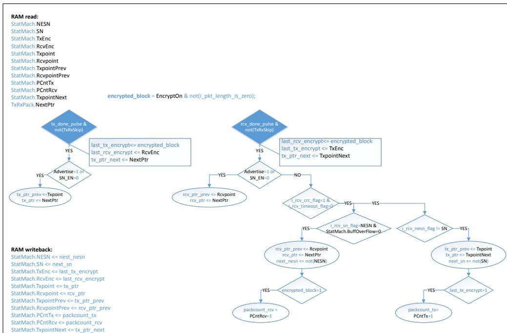
RAM read:
- StatMach.NESN
- StatMach.SN
- StatMach.TxEnc
- StatMach.RevEnc
- StatMach.Txpoint
- StatMach.Revpoint
- StatMach.TxpointPrev
- StatMach.RevpointPrev
- StatMach.PCntTx
- StatMach.PCntRcv
- StatMach.TxpointNext
- TxRxPack.NextPtr
encrypted_block = EncryptOn & not(i_pkt_length_is_zero);
Flowchart Logic:
- tx_done_pulse & not(TxRxSkip)
(Decision):
- YES
:
last_tx_encrypt <= encrypted_block,last_rcv_encrypt <= RevEnc,tx_ptr_next <= NextPtr.- Advertise=1 or SN_EN=0
(Decision):
- YES
:
tx_ptr_prev <= Txpoint,tx_ptr <= NextPtr.
- YES
:
- Advertise=1 or SN_EN=0
(Decision):
- YES
:
- rcv_done_pulse & not(TxRxSkip)
(Decision):
- YES
:
last_rcv_encrypt <= encrypted_block,last_tx_encrypt <= TxEnc,tx_ptr_next <= TxpointNext.- Advertise=1 or SN_EN=0
(Decision):
- YES
:
rcv_ptr_prev <= Revpoint,rcv_ptr <= NextPtr. - NO
:
- L_rcv_orc_flag=1 & L_rcv_timeout_flag=0
(Decision):
- YES
:
L_rcv_sn_flag=NESN & StatMach.BuffOverflow=0
(Decision):
- YES
:
rcv_ptr_prev <= Revpoint,rcv_ptr <= NextPtr,next_nesn <= not(NESN).- encrypted_block=1
(Decision):
- YES
:
packcount_rcv = PCntRcv-1.
- YES
:
- encrypted_block=1
(Decision):
- NO
:
L_rcv_nesn_flag != SN
(Decision):
- YES
:
tx_ptr_prev <= Txpoint,tx_ptr <= TxpointNext,next_sn <= not(SN).- last_tx_encrypt=1
(Decision):
- YES
:
packcount_tx = PCntTx-1.
- YES
:
- last_tx_encrypt=1
(Decision):
- YES
:
- YES
:
- YES
:
L_rcv_sn_flag=NESN & StatMach.BuffOverflow=0
(Decision):
- L_rcv_orc_flag=1 & L_rcv_timeout_flag=0
(Decision):
- YES
:
- Advertise=1 or SN_EN=0
(Decision):
- YES
:
RAM writeback:
- StatMach.NESN <= next_nesn
- StatMach.SN <= next_sn
- StatMach.TxEnc <= last_tx_encrypt
- StatMach.RevEnc <= last_rcv_encrypt
- StatMach.Txpoint <= tx_ptr
- StatMach.Revpoint <= rcv_ptr
- StatMach.TxpointPrev <= tx_ptr_prev
- StatMach.RevpointPrev <= rcv_ptr_prev
- StatMach.PCntTx <= packcount_tx
- StatMach.PCntRcv <= packcount_rcv
- StatMach.TxpointNext <= tx_ptr_next
25.8.5.2 Channel number management
The Bluetooth LE link layer manages the channel frequency through different parameters located in the RAM table.
A channel incrementer allows calculating a new channel if TxRxPack.IncChan bit is set. The algorithm (#1 or #2) is selected through the TxRxPack.ChanAlgo2Sel bit.
In addition, a remap is done to fit with the StatMach.UserChannelFlags if TxRxPack.IncChan bit is set.
Figure 206. Bluetooth LE link layer channel management overview presents an overview of the channel number management.
Figure 206. Bluetooth LE link layer channel management overview
![Figure 206. Bluetooth LE link layer channel management overview. This block diagram shows the internal logic for channel management. Inputs include 'advertise', 'ChanAlgo2Sel', 'Uchan[5:0]', 'hopInc[5:0]', 'EventCounter[15:0]', 'SubEventChanAlgo2', 'UsedChannelFlags[36:0]', and 'Remap_Chan[5:0]'. The logic involves an AND gate for advertising, an incrementer for Algorithm #1, and a complex PRNG and incrementer block for Algorithm #2. Multiplexers select between these algorithms based on control signals. The final output 'UChan' is written back to a RAM table, while 'Remap_Chan' is passed through a LUT to become the 'Physical channel'. A color legend defines signal types: Purple for data read from RAM, Dark red for data written back to RAM, Dark orange for links to primary advertise, Green for links to Algorithm #1, and Blue for links to Algorithm #2.](/RM0529-STM32WB05xZ/80704d0386b35daa44b14ec641410117_img.jpg)
When the channel incrementer hardware block is used (IncChan = 1), the selection of the algorithm must be managed by the SW following Table 235. Truth table to select the correct algorithm below.
Table 235. Truth table to select the correct algorithm
| TxRxPack | Selected algorithm | ||
|---|---|---|---|
| Advertise | ChanAlgo2Sel | SubEventChanAlgo2 | |
| 0 | 0 | X | Algorithm #1 is used for the channel hopping for data channel. |
| 1 | 0 | X | Primary advertising channels selected with automatic incrementation as follows: 37 → 38 → 39 → 37 → 38... Note: this configuration should not be used when running on secondary advertising channels (undefined behavior). |
| 0 | 1 | 0 | Algorithm #2 for an event channel (connection, secondary Advertising or CIS/BIS event) is used for the channel hopping for data channel. |
| 0 | 1 | 1 | Algorithm #2 for a subevent channel (for example CIS/BIS subevent) is used for the channel hopping for data channel. |
| 1 | 1 | 0 | Algorithm #2 is used for the channel hopping for Periodic Advertising channel. Note: this configuration should not be used when running on primary advertising channels (undefined behavior). |
| 1 | 1 | 1 | Not supposed to be used with Bluetooth specification/use-cases. |
In addition, the following table lists the different bit field in RAM tables linked to the channel number management and indicates which ones are used at hardware level according to targeted algorithm (#1 or #2).
Table 236. RAM table bit fields usage versus algorithm number
| Bit field | RAM table | Read/write-back | Considered | |
|---|---|---|---|---|
| for Algo #1 | for Algo #2 | |||
| InChan | TxRxPack | Read | Yes | Yes |
| ChannelAlgo2Sel | TxRxPack | Read | Yes | Yes |
| EventCounter[15:0] | StatMach | Read | No | Yes |
| SubEventChanAlgo2 | TxRxPack | Read | No | Yes |
| advertise | TxRxPack | Read | Yes | Yes |
| accaddr[31:0] | StatMach | Read | No | Yes |
| UsedChannelFlags[36:0] | StatMach | Read | Yes | Yes |
| hopincr[5:0] | StatMach | Read | Yes | No |
| UChan[5:0] | StatMach | Read / Written back | Yes | No |
| Remap_chan[5:0] | StatMach | Read / Written back | Yes | Yes |
25.8.5.3 Time capture
The IP_BLE can capture the absolute time on specific events.
The capture feature is enabled inside the RAM tables and the result is provided in an IP_BLE APB register called TIMECAPTUREREG[31:0].
The events that can be time stamped / captured are:
- • Sequencer reaches the end of 1 st INIT step ( InitDelay timeout)
- • Sequencer reaches the end of DATA INIT step ( init_radio_delay timeout)
- • “On the air” last bit transmitted/received bit (depending on Rx or Tx current mode)
- • Preamble + Access Address detection event on a reception
The time capture service is associated to an interrupt flag that is enabled through the TxRxPack.IntTimeCapture bit and status / interrupt flag at the end of the sequence is available in the IP_BLE APB STATUSREG.TIMECAPTURETRIG (and INTERRUPT1REG.TIMECAPTURETRIG if interrupt is enabled inside the TxRxPack table).
If several events are requested to be captured on a same sequence (e.g. Sequencer reaches end of 1 st INIT and “on the air” last bit), the latest occurrence is the available time inside the TIMECAPTUREREG register.
On a transmission sequence:
Table 237. Transmission sequence
| GlobStatMach | TxRxPack | IP_BLE APB | ||
|---|---|---|---|---|
| TimeCapture | TimeCaptureSel | TrigRcv | TrigDone | TIMECAPTUREREG |
| 0 | x | x | 0 | Sequencer end of 1 st INIT |
| 1 | 0 | x | 0 | Sequencer end of 1 st INIT |
| 1 | 1 | x | 0 | Sequencer end of DATA INIT |
| x | x | x | 1 | “On the air” last transmitted bit |
Table 238. Reception sequence
| GlobStatMach | TxRxPack | IP_BLE APB | ||
|---|---|---|---|---|
| TimeCapture | TimeCaptureSel | TrigRcv | TrigDone | TIMECAPTUREREG |
| 0 | x | 0 | 0 | Sequencer end of 1 st INIT |
| 1 | 0 | 0 | 0 | Sequencer end of 1 st INIT |
| 1 | 1 | 0 | 0 | Sequencer end of DATA INIT |
| x | x | 1 | 0 | Preamble + Access Address detection time |
| x | x | x | 1 | "On the air" last received bit |
25.8.5.4 Sequencer timings recommended values
The 2 nd INIT and DATA INIT steps of the Sequencer use several timing parameters in addition to the init_radio_delay. This generic name covers 4 different durations depending on the transfer configuration (Tx/Rx, PLL calibration/No calibration).
For reminder, the Radio FSM and the Sequencer run in parallel with almost no handshake from the start of the 2 nd INIT phase.
A set of timings is programmed in the GlobalStatMach to guarantee the Sequencer starts the transmission (respectively reception) phase with respect to the Radio FSM progress.
Figure 207. Timings of an Rx sequence and Figure 208. Timings of a Tx sequence show a summary of involved timings.
Figure 207. Timings of an Rx sequence
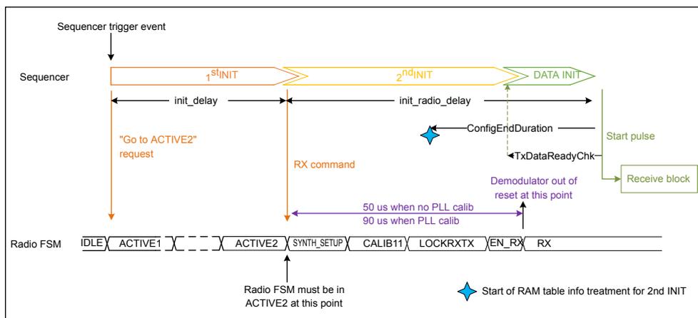
Figure 208. Timings of a Tx sequence
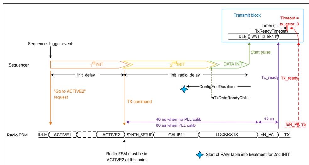
The diagram shows the timing of a transmit (Tx) sequence across three main components: Sequencer, Radio FSM, and Transmitter block.
- Sequencer:
Starts with a "Sequencer trigger event". It executes three steps:
1
st
INIT,
2
nd
INIT, and DATA INIT.
- The
1
st
INIT step has a duration of
init_delay. At its end, a "Go to ACTIVE2" request is sent to the Radio FSM. - The
2
nd
INIT step has a duration of
init_radio_delay. At its end, a "TX command" is sent to the Radio FSM. - The DATA INIT step ends at a point labeled "ConfigEndDuration".
- The
1
st
INIT step has a duration of
- Radio FSM:
Transitions through states: IDLE → ACTIVE1 → ACTIVE2 → SYNTH_SETUP → CALIB11 → LOCKRXTX → EN_PA → TX.
- A note indicates: "Radio FSM must be in ACTIVE2 at this point" when the TX command is received.
- Another note indicates: "Start of RAM table info treatment for 2nd INIT" occurs during the 2 nd INIT step.
- Timing from TX command to EN_PA state: "40 us when no PLL calib" or "80 us when PLL calib".
- Timing from EN_PA to TX state: "12 us".
- Transmitter block:
Contains a state machine with IDLE and WAIT_TX_READY states.
- A "Start pulse" is sent from the DATA INIT step to the IDLE state.
- A "Tx_ready" signal is sent from the WAIT_TX_READY state back to the Sequencer.
- A "Timeout = tx_error_3" is generated if the "TxReadyTimeout" timer expires while in the WAIT_TX_READY state.
Reminder on main constraints for a transmission:
- the DATA_INIT step must end before the Radio FSM reaches the Tx state.
- it is possible to take some margin as the TxReadyTimeout delay allows waiting for the confirmation that the Radio FSM is in Tx state before really starting the TxDelayStart timeout (see Figure 202. Tx sequence).
- if TxRxPack.IncChan = 0, the Sequencer reads the PaPower[4:0] information from the RAM table only after the ConfigEndDuration temporization.
- the ConfigEndDuration value must be big enough to ensure the Sequencer treats this information before the Radio FSM reaches the EN_PA state.
Reminder on main constraints for a reception:
- the DATA_INIT step must end close to the moment the Radio FSM reaches the Rx state as it corresponds to the start of the Receive timeout window.
- the Sequencer transfers the StatMach.accaddr information in the AA0_DIG_USR to AA3_DIG_USR radio registers for the demodulator block. This transfer in the radio register is done only after the ConfigEndDuration temporization. This information is used by the demodulator and must be present before the Radio FSM reaches the Rx state.
- the ConfigEndDuration value must be big enough to ensure the Sequencer starts the activity before the Radio FSM reaches the Rx state.
Table 239. Delays for Sequencer 2 nd INIT step proposal shows some recommendations/proposals on values for some timings programmed through RAM tables.
Table 239. Delays for Sequencer 2 nd INIT step proposal
| GlobalStatMach table bit field | Recommended value | Comments |
|---|---|---|
| TransmitNoCalDelayChk[7:0] | 0x32 (50d) | Theoretical exact duration from ACTIVE2 to Tx state is 52 µs. Keep some margin to avoid timeout after Tx state. Then, use the TxReadyTimeout[7:0] to define the duration of the wait Tx state info for the transmit block. |
| TransmitCalDelayChk[7:0] | 0x5A (90d) | Theoretical exact duration from ACTIVE2 to Tx state is 92 µs. Keep some margin to avoid timeout after Tx state. Then, use the TxReadyTimeout[7:0] to define the duration of the wait Tx state info for the transmit block. |
| ReceiveNoCalDelayChk[7:0] | 0x32 (50d) | Theoretical exact duration from ACTIVE2 to Rx state is 50 µs. The delay can be programmed to 50us. |
| GlobalStatMach table bit field | Recommended value | Comments |
|---|---|---|
| ReceiveCalDelayChk[7:0] | 0x5A (90d) | Theoretical exact duration from ACTIVE2 to Rx state is 90 µs. The delay can be programmed to 90 µs. |
| ConfigEndDuration[7:0] | at least 10 max is init_radio_delay | Note:
|
| TxDataReadyCheck[7:0]k | between 1 and 5 | Can be increased to take more margin. Only impact is a potential useless extra waiting time before aborting when the Radio FSM / the sequence is broken. |
| TxReadyTimeout[7:0] | at least 5 | Can be increased to take more margin. Only impact is the Tx sequence abort is delayed with the same additional delay in case of real Radio FSM Tx sequence issue. |
25.8.6 Angle of arrival (AoA) and angle of departure (AoD)
The Bluetooth Core Specification v5.1 introduces new capabilities that support higher-accuracy direction finding. The Bluetooth direction finding exploits some of the fundamental properties of radio waves by taking several phases and amplitude measurements (across different antenna) that can be used in direction finding calculations at precise intervals in a process known as In-phase and Quadrature Sampling (IQ sampling).
Applications use this data in calculations that involve trigonometry and information about the design of the antenna array.
A single IQ sample consists of the wave's amplitude and phase angle represented as a set of Cartesian coordinates. Applications can transform this Cartesian representation into corresponding polar coordinates that yield the phase angle and the amplitude value.
The existing RAM tables have been upgraded to support the new hardware features (CTE, I/Q sampling and Antenna Switching) added to support the direction-finding topic.
25.8.6.1 RAM tables and registers impact
The existing RAM tables have been upgraded to support the new hardware features (CTE, I/Q sampling and Antenna Switching) added to support the direction-finding topic.
25.8.6.1.1 GlobalStatMatch RAM table
The GlobalStatMach table size has not been impacted: still 7 words = 28 bytes.
A new bit field has been added in the RFU existing Word6: DefaultAntennaId[6:0] bit field in Word6[6:0].
This bit field is mandatory for the configurations where more than one antenna is present on the board.
This bit field indicates which antenna identifier must be used to transmit or receive packets without CTE or packet body (Preamble, Access Address, PDU, and CRC) for CTE enabled packets. This value is transmitted through the corresponding pads of the device to the external component located on the board to switch on the requested antenna.
25.8.6.1.2 StatMach RAM table
The StatMach RAM table size has been increased by 3 words for a total of 23 words = 92 bytes.
The additional bit fields are the following:
- CTEDisable bit in Word0[27]. If set,
- in transmission: no CTE appended at the end of the Frame whatever the TxRxPack.CTEAndSamplingEnable bit value
- in reception: no CTE detection nor treatment done on the PDU, frame treated as a Bluetooth® LE core 5.0 or less format.
- • CTETIME[4:0] bit field in Word14[6:2]:
- – used only when StatMach.CTEDisable=0, TxRxPack.CTEAndSamplingEnable=1 and StatMach.TxMode=1 ,
- – same format as the CTEInfo CTETIME bit field (time unit = 8 µs),
- – provides the duration of the Constant Tone Extension to append after CRC.
- • CTESlotWidth bit in Word14[1]:
- – in transmission and AoD use-case: used to control the antenna switching timing,
- – in reception and in AoA use-case: used to control the antenna switching and the I/Q sampling timings,
- – not needed in other configurations,
- – used only when StatMach.CTEDisable=0, TxRxPack.CTEAndSamplingEnable=1 .
- • MaximumIQSamplesNumber[6:0] bit field in Word14[14:8]:
- – needed in reception only to indicate the maximum I/Q samples that can be stored in RAM,
- – if more I/Q samples are received (CTE time longer than maximum samples allowed), the sequence goes on but the AHB master stops storing the additional receive samples.
- – used only when StatMach.CTEDisable=0, TxRxPack.CTEAndSamplingEnable=1 and StatMach.TxMode=0 .
- • IQSamplesPtr[31:0] bit field in Word15[31:0]:
- – needed in reception only to indicate the start address in RAM to store the I/Q samples received during the CTE,
- – the address contained by this pointer must be 32-bit aligned and MSByte value must be equal to the MSByte of the RAM base address of the device,
- – used and verified only when StatMach.CTEDisable=0, TxRxPack.CTEAndSamplingEnable=1, StatMach.TxMode=0 and StatMach.MaximumIQsamplesNumber >0 .
- • AntennaPatternLength[7:0] bit field in Word14[23:16]:
- – needed when antenna switching must be managed on the current transfer (in transmission if AoD / in reception if AoA),
- – defines the length of the Antenna ID pattern to be applied during the CTE. If the CTE duration requires more slots than the length defined here, the same pattern is repeated until the end of the CTE phase,
- – used only when StatMach.CTEDisable=0 and TxRxPack.CTEAndSamplingEnable=1 .
- • AoD_nAoA bit in Word14[0]:
- – used only when StatMach.CTEDisable=0, TxRxPack.CTEAndSamplingEnable=1 and StatMach.TxMode=1 ,
- – indicates to the transmitter if it has to manage antenna switching (AoD) or not (AoA) during the transmission when CTE is enabled.
- • AntennaPatternPtr[31:0] bit field in Word16[31:0]:
- – needed when antenna switching has to be managed to indicate the start address of the antenna pattern (the antenna pattern is a list of 8-bit values describing the antenna identifier),
- – the RAM location addressed by the StatMach.AntennaPatternPtr shall contain at least StatMach.AntennaPatternLength bytes,
- – used and verified only when StatMach.CTEDisable=0, TxRxPack.CTEAndSamplingEnable=1 and StatMach.AntennaPatternLength>0 .
25.8.6.1.3 TxRxPack RAM table
The TxRxPack RAM table size has been decreased by 1 word for a total of 4 words = 16 bytes.
A new CTEAndSamplingEnable bit has been added in Word1[3]. The role of this bit is to indicate to the MR_BLE IP:
- • In transmission:
- – to append a Constant Tone Extension after the CRC
- – to manage the antenna switching if AoD use-case
- • In reception:
- – to detect if the received frame has a CTE and to extract details from the CTEInfo
- – to manage the I/Q Sampling storage in RAM
- – to manage the antenna switching if AoA use-case.
25.8.6.2 Manage the feature in transmission
If the SW wants to append a Constant Tone Extension at the end of the frame, it has to:
- • ensure the StatMach.CTEDisable bit is 0,
- • program the CTE duration in the StatMach.CTETIME[4:0] (same format as the CTETIME bit field of the CTEInfo defined by the standard),
- • set the TxRxPack.CTEAndSamplingEnable = 1 for this dedicated packet.
In case of encrypted frame, the AES encrypts or not the HEADER3 thanks to the TxRxPack.Advertise information.
Note:
The transmit block does not decode on the fly the bytes provided by the RAM Data Buffer (located at DataPtr address) to identify the CTE information. It relies on the information provided through the RAM table. It is the responsibility of the SW to guarantee the coherency between the CTE related bit field in RAM and the data in RAM that corresponds to the CTEInfo bit field inside the frame on the air.
In addition to the CTE append on the transmitted frame, if the device must manage the antenna switching (AoD configuration), the SW has to:
- • define the default Antenna ID for the packet body through the GlobalStatMach.DefaultAntennaId[6:0] bit field,
- • provide the start address of the antenna pattern through the StatMach.AntennaPatternPtr[31:0] bit field,
- • provide the antenna pattern / sequence length through the StatMach.AntennaPatternLength[7:0] bit field,
- • fill the RAM location pointed by the StatMach.AntennaPatternPtr[31:0] bit field with 8-bit antenna identifier (the SW must ensure this RAM area contains at least StatMach.AntennaPatternLength[7:0] antenna ID),
- • if needed, tune the TX_TIME_TO_SWITCH[6:0] timing in the ANTSW2_DIG_USR radio register to compensate potential delay between the modulator to antenna path versus antenna switching component control signals.
In parallel, the SW must ensure the SoC GPIOs have been programmed in the accurate configuration to output the Antenna Identifier and enable signals to the external component.
Note: To execute a transmission without CTE phase appended at the end of the frame, the SW just must set the StatMach.CTEDisable bit to 1.
25.8.6.3 Manage the feature in reception
25.8.6.3.1 CTE detection and decoding
If the SW wants the MR_BLE to execute a reception with the ability to detect if the received frame is a packet with or without CTE, it has to:
- • set the StatMach.CTEDisable bit to 0,
- • set the TxRxPack.CTEAndSamplingEnable bit to 1.
In case of encrypted frame, the AES decrypts or not the HEADER3 thanks to the TxRxPack.Advertise information.
Table 240. Behavior versus CTEDisable and CTEAndSampling bits value shows the behavior according to the combination between TxRxPack.CTEAndSamplingEnable and StatMach.CTEDisable .
Table 240. Behavior versus CTEDisable and CTEAndSampling bits value
| Configuration | Behavior |
|---|---|
| StatMach.CTEDisable = 1 and TxRxPack.CTEAndSamplingEnable = “don’t care” | The receiver behaves as a Bluetooth® LE SIG 5.0 or before.
|
| Configuration | Behavior |
|---|---|
| |
| StatMach.CTEDisable = 0 and TxRxPack.CTEAndSamplingEnable = 0 | The receiver detects if CTE packet or not but does not sample the I/Q. This configuration allows keeping the synchronization on T IFS with the transmitting device.
|
| StatMach.CTEDisable = 0 and TxRxPack.CTEAndSamplingEnable = 1 | The receiver detects if CTE packet or not and manages the I/Q sampling.
|
During the reception, the receiver extracts from the frame the CTE info like duration, slot width and type. The only configuration for which the MR_BLE needs to get the information from the RAM table is the Angle of Arrival (AoA). In this specific case, the slot width is not indicated in the CTEType[1:0] bit field:
- 00: AoA
- 01: AoD with 1 µs slots
- 10: AoD with 2 µs slots
- 11: reserved for future use
In AoA, the receiver device is the owner of the antenna switching and of the time slot width choice. In this specific configuration, the SW must provide the information through the StatMach.CTESlotWidth bit.
25.8.6.3.2 I/Q sampling
The MR_BLE stores the I/Q samples in words built as follows:
- I[15:0] as 16 MSbit
- Q[15:0] as 16 LSbit
As the AHB master writes both I and Q in one 32-bit access in RAM, the IQSamplesPtr must contain a 32-bit aligned address.
To manage a reception in CTE with I/Q sampling, the SW has:
- to set the reception has CTE aware (refer to previous sub-section),
- to program the maximum number of I/Q samples that are allowed to be written in RAM (between 0 and 127 I+Q) through the StatMach.MaximumIQSamplesNumber[6:0] bit field,
- to define the start address to store the I/Q samples in the StatMach.IQSamplesPtr[31:0] .
At the end of the reception, some status bit fields are provided to give visibility on what has been received:
- IP_BLE APB register called STATUS2REG [0] = IQSamplesReady.
- when set, indicates I/Q sampling has been received
- when set, means that the received frame embedded a Constant Tone Extension at the end
- IP_BLE APB register called STATUS2REG [7:1] = IQSamplesNumber[6:0]
- provides the number of I/Q samples stored in RAM.
25.8.6.3.3 Antenna switching
In addition to the CTE detection and the I/Q sampling storage, in AoA, the device has to manage the antenna switching. To achieve this, the SW has to:
- define the default Antenna ID for the packet body through the GlobalStatMach.DefaultAntennaId[6:0] bit field,
- • provide the start address of the antenna pattern through the StatMach.AntennaPtr[31:0] bit field,
- • provide the antenna pattern / sequence length through the StatMach.AntennaLength[7:0] bit field,
- • fill the RAM location pointed by the StatMach.AntennaPtr[31:0] bit field with 8-bit antenna identifier (the SW must ensure this RAM area contains at least StatMach.AntennaLength[7:0] antenna ID),
- • if needed, tune the RX_TIME_TO_SWITCH[5:0] timing in the ANTSW1_DIG_USR radio register to compensate potential delay between antenna path to demodulator versus antenna switching component control signals,
- • if needed, tune the RX_TIME_TO_SAMPLE[6:0] timing in the ANTSW0_DIG_USR radio register to center the I/Q sampling action inside the slot window.
In parallel, the SW must ensure the SoC GPIOs have been programmed in the accurate configuration to output the Antenna Identifier and enable signals to the external component.
Note: The hardware automatically restarts the antenna switching pattern from its first element if there are more CTE slots than the AntennaLength value provided in the StatMach.
25.8.6.4 Error management
Several error cases are treated at hardware level concerning CTE, I/Q sampling and antenna switching.
25.8.6.4.1 Invalid CTEType received
Expected values for the CTEType[1:0] bit field inside the CTEInfo are “00”, “01” or “10”. If the receiver decodes a CTEType[1:0] = “11” in a CTE packet, it behaves as if TxRxPack.CTEAndSamplingEnable = 0 (CTE time duration respected for reception phase but no I/Q sampling nor antenna switching management).
25.8.6.4.2 CTE length outside [20..2] window
The MR_BLE IP has been designed to support CTE length outside the standard limit to offer the possibility to develop proprietary versions or for trials in lab.
In reception:
- • if CTE length > 20:
- – the reception is able to manage I/Q sampling and CTE phase for CTE length greater than the standard. For I/Q sampling, the limit used by the hardware is the StatMach.MaximumIQSamplesNumber bit field value.
- • if CTE length < 2:
- – the reception is able to manage I/Q sampling and CTE phase for CTE length less than the standard.
In transmission:
- • if CTE length > 20:
- – the transmission is able to manage a CTE duration longer than the longest indicated by the Bluetooth core specification 5.1 standard.
- – the TXERROR_4 flag (and associated interrupt if enabled) is raised to inform the packet is not CTE standard compliant (but the transmission is executed with requested configuration).
- • if CTE length < 2:
- – the transmission is able to manage a CTE duration shorter than the shortest indicated by the Bluetooth core specification 5.1 standard. Note that for duration = 0, this is equivalent to no CTE phase after CRC.
- – the TXERROR_4 flag (and associated interrupt if enabled) is raised to inform the packet is not CTE standard compliant (but the transmission is executed with requested configuration).
25.8.6.4.3 CTE requested while long range is selected
The Bluetooth core specification 5.1 standard indicates the Constant Tone Extension feature does not concern the Coded PHY packets (long range configuration).
If the MR_BLE IP is in front of a contradictory configuration indicating coded PHY format and CTE enabled, the transfer is managed as a Coded PHY without CTE.
In reception, no CTE detection is activated (so no I/Q sampling nor antenna switching is managed either).
In transmission:
- • no CTE phase is appended at the end of the frame,
- the TXERROR_4 flag (and associated interrupt if enabled) is raised to inform the configuration is not CTE standard compliant.
25.8.6.4.4 IQSamplesPtr[31:0] or AntennaPtr[31:0] not 32-bit aligned
The StatMach.IQSamplesPtr[31:0] and the StatMach.AntennaPtr[31:0] must contain a 32-bit aligned address.
For IQSamplesPtr, an error is detected if:
- the StatMach.IQSamplesPtr[31:0] does not contain a modulo 4 value (32-bit aligned address),
- and StatMach.CTEDisable=0,
- and StatMach.CTEAndSamplingEnable=1,
- and StatMach.MaximumIQSamplesNumber[6:0] > 0.
For AntennaPtr, an error is detected if:
- the StatMach.AntennaPtr[31:0] does not contain a modulo 4 value (32-bit aligned address),
- and StatMach.CTEDisable=0,
- and StatMach.CTEAndSamplingEnable=1,
- and StatMach.AntennaPtrLength[7:0] > 0.
The associated error is a ConfigError (no RF transfer as the Sequencer aborts after the 1st INIT step). Refer to Section 25.8.2.3.4: Configuration error for details on the ConfigError behavior.
25.8.6.4.5 IQSamplesPtr[31:24] or AntennaPtr[31:24] not equal to device RAM base address[31:24]
The StatMach.IQSamplesPtr[31:24] and the StatMach.AntennaPtr[31:24] must contain a value equal to the RAM base address[31:24].
For IQSamplesPtr, an error is identified if:
- the StatMach.IQSamplesPtr[31:24] is different from the RAM base address[31:24],
- and StatMach.CTEDisable=0,
- and StatMach.CTEAndSamplingEnable=1,
- and StatMach.MaximumIQSamplesNumber > 0.
For AntennaPtr, an error is detected if:
- the StatMach.AntennaPtr[31:24] is different from the RAM base address[31:24],
- and StatMach.CTEDisable=0,
- and StatMach.CTEAndSamplingEnable=1,
- and StatMach.AntennaPtrLength[7:0] > 0.
The associated error is an AddPointError (no RF transfer as the Sequencer aborts after the 1st INIT step). Refer to Section 25.8.2.3.5: Address pointer error for details on the AddPointError behavior.
25.8.6.4.6 I/Q sampling storage overflow
In case of too high latency in AHB transfers between the MR_BLE IP and the RAM inside the device, some received I/Q samples could be overwritten inside the internal buffer before being transferred into the SoC RAM.
In this case:
- a status flag is raised in the STATUS2REG IP_BLE APB register: STATUS2REG [29] = IQSamplesMissingError,
- no more I/Q samples are written in RAM until the end of the CTE phase,
- the IQSamplesReady bit and the IQSamplesNumber bit fields are updated according to the real number of samples written in RAM,
- the rest of the reception goes on in a normal way (including antenna switching is AoA, despite no more samples being recorded).
Then, the SW has the choice to handle or not the partial list of received I/Q samples.
Note: This error is not supposed to occur as an internal FIFO has been put in place to buffer some I/Q samples and is supposed to be dimensioned according to the device bandwidth.
25.8.6.4.7 Antenna pattern length=1
The Bluetooth core specification 5.1 for the HCI_LE_Set_Connection_CTE_Receive_Parameters indicates the Length_of_switching_Pattern parameter must be at least 2, the MR_BLE IP, at hardware level, supports an antenna pattern length=1.
In this case, the reference period and the sample slots are done on the same antenna.
25.8.6.4.8 Antenna pattern read underflow
In case of too high latency in AHB transfers between the MR_BLE IP and the RAM inside the device, the next antenna ID may not be ready inside the antenna switching sub-block when the next antenna switching event is supposed to occur.
In this case:
- • a flag is raised in the STATUS2REG IP_BLE APB register: STATUS2REG [30] = AntennaSwitchingPatternAccessError
- • the antenna switching process goes on but with an unpredictable value on the antenna ID and shifted value once the read value is available.
Note: this error is not supposed to occur as an internal FIFO is present to store some anticipated antenna ID and is supposed to be dimensioned according to the device bandwidth.
25.8.7 AES
The MR_BLE IP embeds an AES hardware accelerator. This accelerator is encapsulated in a wrapper allowing a single accelerator core to be shared for 3 different actions/modes:
- 1. on-the fly encryption
- 2. manual encryption
- 3. LE privacy
In case of simultaneous requests for several modes, a priority mechanism serves the requester in the same order as the list order above.
25.8.7.1 On the fly encryption
This mode corresponds to an on-going Bluetooth encrypted transmission/reception.
In transmission, the AES encrypts the data read from the RAM DataPack table before transmitting them.
In reception, the AES decrypts the received data before storing them in the DataPack RAM table.
This mode is activated as soon as an RF transfer is done with the StatMach.EncryptOn bit set to '1'.
The on the fly AES feature can discriminate the part of the frame not concerned by encryption like the HEADER parts (including the HEADER3 when CTE is active in the frame).
Warning: the isochronous channels encryption is not managed by this hardware feature and needs to be done at SW level without enabling the hardware encryption.
This mode is the most priority mode and is always served first in case of concurrent requests not to impact the Bluetooth communication.
25.8.7.2 Manual encryption
The goal of this mode is to share the AES core embedded with the CPU of the SoC. As the Bluetooth® LE link layer does not use this hardware resource all the time, the idea is to let the CPU process its own encryptions through this hardware accelerator. It avoids adding an extra AES core to the SoC if the share usage is acceptable.
A set of registers is present to manage this manual encryption (see Section 25.8.9.1: IP_BLE controller register list ).
The process to fulfill a manual encryption is the following:
- 1. Enter the key in the MANAESxKEYREG registers (x from 0 to 3).
- 2. Enter the text to encrypt (16 bytes by computation) in the MANAESCLEARTEXTxREG (x from 0 to 3) registers.
- 3. Possibility to enable an interrupt to be informed when the computation is over by setting the MANAESCMDREG[1] = INTENA bit.
- 4. Launch the encryption by setting the MANAESCMDREG[0] = START bit.
- 5. Wait for end of computation:
- a. If the interrupt mode is enabled, the interrupt line dedicated to AES (irq_BLE_int2 aka BLE_AES) is raised and the CPU gets the reason in the Interrupt2Reg[0] = AESMANENDINT bit.
- b. Otherwise, the SW has to poll the MANAESSTATREG[0] = BUSY bit until it is cleared by hardware.
- 6. If interrupt is used, write 1 in the Interrupt2Reg[0] = AESMANENDINT bit to clear the flag.
- 7. The encrypted data / result is available in the MANAESCYPTERTEXTxREG (x from 0 to 3) registers.
- 8. If needed, the SW can restart from step 1 or step 2.
25.8.7.3 LE privacy
In MR_BLE IP, the Bluetooth® LE link layer controller provides a hardware solution for the LE privacy resolution. The process to fulfill the LE privacy resolution is the following:
- 1. The processor must provide the AES block with:
- a. the address in RAM where to find the 128-bit key array through the AESLEPRIVPOINTERREG IP_BLE APB register.
- b. the reference HASH through the AESLEPRIVHASHREG IP_BLE APB register.
- c. the random number through the AESLEPRIVPRANDREG IP_BLE APB register.
- d. the maximum key number through the AESLEPRIVCMDREG IP_BLE APB register (NBKEYS bit field).
- 2. Enable the AES LE privacy interrupt by setting the INTENA bit in the AESLEPRIVCMDREG IP_BLE APB register.
- 3. Launch the calculation by setting the Start bit in the AESLEPRIVCMDREG IP_BLE APB register (auto-cleared bit).
- 4. At the end of computation, the interrupt line dedicated to AES (irq_BLE_int2 aka BLE_AES) is raised and the CPU gets the reason in the INTERRUPT2REG [1] = AESLEPRIVINT bit.
- 5. Write 1 in the INTERRUPT2REG[1] = AESLEPRIVINT bit to clear the flag.
- 6. The results are then available in the following registers / bit fields:
- a. the KEYFIND bit in the AESLEPRIVSTATREG IP_BLE APB register indicates if a key has been found (KEYFIND bit = 1) or not (KEYFIND) = 0 in the list,
- b. if KEYFIND = 1, the KEYFINDINDEX[7:0] bit field in the AESLEPRIVSTATREG IP_BLE APB register indicates which key of the array is the one found.
25.8.8 MSB first feature
The MSB first feature, not compliant with the Bluetooth standard, is added to extend potential proprietary protocols.
The principle is:
- • in Tx: to swap the endianness inside transmitted bytes before whitening,
- • in Rx: to swap the endianness inside received bytes after dewhitening.
The bit endianness modification is done only on the PDU part of the packet. This means:
- • the PREAMBLE is sent as usual,
- • the bit endianness inversion for the Access Address must be managed at SW level by reverting the endianness of the programmed value in the StatMach.AccAddr[31:0].
However, the MR_BLE receive block is able to manage the 2 first bytes of the PDU regardless of the endianness option:
- • first byte to export its content (LLID, MD, SN, NESN)
- • second byte to correctly extract the length information from the HEADER1
Figure 209. MSBFirst feature principle overview
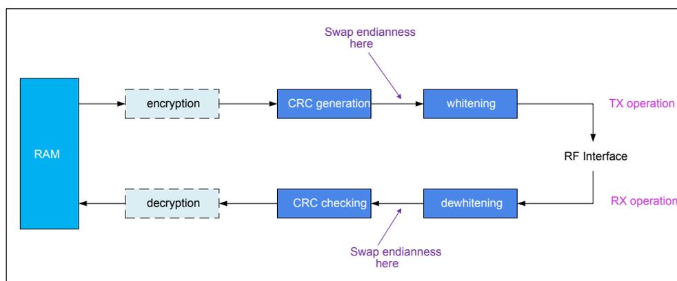
graph LR
    subgraph TX
        RAM[RAM] --> encryption[encryption]
        encryption --> CRC_gen[CRC generation]
        CRC_gen --> whitening[whitenning]
        whitening --> RF[RF Interface]
        RF --> TX_op[TX operation]
    end
    subgraph RX
        RF --> RX_op[RX operation]
        RX_op --> dewhitenning[dewhitenning]
        dewhitenning --> CRC_check[CRC checking]
        CRC_check --> decryption[decryption]
        decryption --> RAM
    end
    CRC_gen -.->|Swap endianness here| whitening
    CRC_check -.->|Swap endianness here| dewhitenning
The feature is enabled by setting the StatMach.MsbFirst bit.
This feature must not be enabled when at least one of the conditions below is true:
- • the packet is in coded PHY format (long range),
- • the CTE mode is enabled (StatMach.CTEDisable=0),
- • the packet is encrypted,
- • StatMach.DisableCRC = 0. Note that in this configuration, either Viterbi must be disabled or packet length=0 cannot be used.
There is no hardware mechanism to ensure previous forbidden configurations are not active at the same time as the MSBFirst feature. So, if the SW does not respect the rule, the integrity of the transfer is not guaranteed.
25.8.9 IP_BLE registers
25.8.9.1 IP_BLE controller register list
The BLUE_BLOCKBaseAddress keyword used for all the register base address information corresponds to the IP_BLE registers base address decided by the SoC when integrating the IP.
Note: BLUE_BLOCKBaseAddress is 0x6000_0000 in the STM32WB05xZ product.
Table 241. IP_BLE controller registers list| Address offset | Name | RW | Reset | Description |
|---|---|---|---|---|
| 0x04 | INTERRUPT1REG | RW | 0x00000000 | INTERRUPT1REG register, related to sources of the irq_BLE_int1, aka BLE_TXRX interrupt line |
| 0x08 | INTERRUPT2REG | RW | 0x00000000 | INTERRUPT2REG register, related to sources of the irq_BLE_int2, aka BLE_AES |
| 0x0C | TIMEOUTDESTREG | RW | 0x00000000 | Timer1 and Timer2 enable/disable |
| 0x10 | TIMEOUTREG | RW | 0x00000000 | Timer1 and Timer2 timeout register |
| 0x14 | TIMERCAPTUREREG | R | 0x00000000 | Timer capture register |
| 0x18 | CMDREG | RW | 0x00000000 | CmdReg register |
| 0x1C | STATUSREG | R | 0x00000000 | Status register |
| 0x20 | INTERRUPT1ENABLEREG | R | 0x00000000 | This read-only register is a copy/summary of all the enable mask bits located in the different RAM tables. When '0', corresponding interrupt was masked during previous sequence. When '1', corresponding interrupt was enabled during the previous sequence. |
| 0x24 | INTERRUPT1LATENCYREG | R | 0x00000000 | Interrupt1 Latency register |
| 0x28 | MANAESKEY0REG | RW | 0x00000000 | Manual AES Key0 register |
| 0x2C | MANAESKEY1REG | RW | 0x00000000 | Manual AES Key1 register |
| 0x30 | MANAESKEY2REG | RW | 0x00000000 | Manual AES Key2 register |
| 0x34 | MANAESKEY3REG | RW | 0x00000000 | Manual AES Key3 register |
| 0x38 | MANAESCLEARTTEXT0REG | RW | 0x00000000 | Manual AES ClearText0 register |
| 0x3C | MANAESCLEARTTEXT1REG | RW | 0x00000000 | Manual AES ClearText1 register |
| 0x40 | MANAESCLEARTTEXT2REG | RW | 0x00000000 | Manual AES ClearText2 register |
| 0x44 | MANAESCLEARTTEXT3REG | RW | 0x00000000 | Manual AES ClearText3 register |
| 0x48 | MANAESCIPHERTEXT0REG | R | 0x00000000 | Manual AES CipherText0 register |
| 0x4C | MANAESCIPHERTEXT1REG | R | 0x00000000 | Manual AES CipherText1 register |
| 0x50 | MANAESCIPHERTEXT2REG | R | 0x00000000 | Manual AES CipherText2 register |
| 0x54 | MANAESCIPHERTEXT3REG | R | 0x00000000 | Manual AES CipherText3 register |
| 0x58 | MANAESCMDREG | RW | 0x00000000 | Manual AES CmdReg register |
| 0x5C | MANAESSTATREG | R | 0x00000000 | Manual AES Status register |
| 0x60 | AESLEPRIVPOINTERREG | RW | 0x00000000 | AES LE Privacy Pointer register |
| 0x64 | AESLEPRIVHASHREG | RW | 0x00000000 | AES LE Privacy Hash register |
| 0x68 | AESLEPRIVPRANDREG | RW | 0x00000000 | AES LE Privacy Prand register |
| 0x6C | AESLEPRIVCMDREG | RW | 0x00000000 | AES LE Privacy CmdReg register |
| 0x70 | AESLEPRIVSTATREG | R | 0x00000000 | AES LE Privacy Status register |
| 0x7C | STATUS2REG | R | 0x00000000 | STATUS2REG register |
25.8.9.2 IP_BLE controller register list description
Table 242. INTERRUPT 1REG register description| Bit | Field name | Reset | RW | Description |
|---|---|---|---|---|
| 3:0 | RESERVED3_0 | 0x0 | R | Reserved |
| 4 | ADDPOINTERERROR | 0x0 | RW | Address Pointer Error. When read, indicates the interrupt status. |
| Bit | Field name | Reset | RW | Description |
|---|---|---|---|---|
| 4 | ADDPONTERERROR | 0x0 | RW | Write 1'b1 to clear. |
| 5 | RXOVERFLOWERROR | 0x0 | RW | Receive Overflow. When read, indicates the interrupt status. Write 1'b1 to clear. |
| 6 | RESERVED6 | 0x0 | R | Reserved |
| 7 | SEQDONE | 0x0 | RW | Sequencer end of task. When read, indicates the interrupt status. Write 1'b1 to clear. |
| 8 | TXERROR_0 | 0x0 | RW | Transmission error 0: transmit block missing data error. When read, indicates the interrupt status. Write 1'b1 to clear. |
| 9 | TXERROR_1 | 0x0 | RW | Transmission error 1: a Tx skip happened during an on-going transmission. When read, indicates the interrupt status. Write 1'b1 to clear. |
| 10 | TXERROR_2 | 0x0 | RW | Transmission error 2: channel index is greater than 39. When read, indicates the interrupt status. Write 1'b1 to clear. |
| 11 | TXERROR_3 | 0x0 | RW | Transmission error 3: error while waiting for the confirmation the Radio FSM is in Tx state. When read, indicates the interrupt status. Write 1'b1 to clear. |
| 12 | TXERROR_4 | 0x0 | RW | Transmission error 4: a CTE issue occurred. When read, indicates the interrupt status. Write 1'b1 to clear. |
| 13 | ENCERROR | 0x0 | RW | Encryption error on receive. When read, indicates the interrupt status. Write 1'b1 to clear. |
| 14 | ALLTABLEREADYERROR | 0x0 | RW | All RAM table not ready on time. When read, indicates the interrupt status. Write 1'b1 to clear. |
| 15 | TXDATAREADYERROR | 0x0 | RW | Transmit data pack not ready error . When read, indicates the interrupt status. Write 1'b1 to clear. |
| 16 | NOACTIVEERROR | 0x0 | RW | GlobStatMach.active bit error. When read, indicates the interrupt status. Write 1'b1 to clear. |
| 17 | RESERVED17 | 0x0 | RW | Reserved |
| 18 | RCVLENGTHERROR | 0x0 | RW | Receive length error. When read, indicates the interrupt status. Write 1'b1 to clear. |
| 19 | SEMETIMEOUTERROR | 0x0 | RW | Semaphore timeout error. When read, indicates the interrupt. Write 1'b1 to clear. |
| Bit | Field name | Reset | RW | Description |
|---|---|---|---|---|
| 20 | RESERVED20 | 0x0 | RW | Reserved |
| 21 | TXRXSKIP | 0x0 | RW | Transmission/Reception skip. |
| When read, indicates the interrupt status. | ||||
| Write 1'b1 to clear. | ||||
| 22 | ACTIVE2ERROR | 0x0 | RW | Active2 Radio state error. |
| When read, indicates the interrupt status. | ||||
| Write 1'b1 to clear. | ||||
| 23 | CONFIGERROR | 0x0 | RW | Data pointer configuration error. |
| When read, indicates the interrupt status. | ||||
| Write 1'b1 to clear. | ||||
| 24 | TXOK | 0x0 | RW | Previous transmitted packet received OK by the peer device. |
| When read, indicates the interrupt status. | ||||
| Write 1'b1 to clear. | ||||
| 25 | DONE | 0x0 | RW | Receive/Transmit done. |
| When read, indicates the interrupt status. | ||||
| Write 1'b1 to clear. | ||||
| 26 | RCVTIMEOUT | 0x0 | RW | Receive timeout (no preamble found). |
| When read, indicates the interrupt status. | ||||
| Write 1'b1 to clear. | ||||
| 27 | RCVNOMD | 0x0 | RW | Received low MD bit. |
| When read, indicates the interrupt status. | ||||
| Write 1'b1 to clear. | ||||
| 28 | RCVCMD | 0x0 | RW | Received command. |
| When read, indicates the interrupt status. | ||||
| Write 1'b1 to clear. | ||||
| 29 | TIMECAPTURETRIG | 0x0 | RW | A time has been captured in TIMERCAPTUREREG. |
| When read, indicates the interrupt status. | ||||
| Write 1'b1 to clear. | ||||
| 30 | RCVRCERR | 0x0 | RW | Receive data fail . |
| When read, indicates the interrupt status. | ||||
| Write 1'b1 to clear. | ||||
| 31 | RCVOK | 0x0 | RW | Receive data OK. |
| When read, indicates the interrupt status. | ||||
| Write 1'b1 to clear. |
Note: All bits with the corresponding enable mask at '0' are seen at '0' in this register whatever the status. The full unmasked status is visible in the STATUSREG register. Refer to STATUSREG for exhaustive flag description.
Table 243. INTERRUPT2REG register description
| Bit | Field name | Reset | RW | Description |
|---|---|---|---|---|
| 0 | AESMANENCINT | 0x0 | RW | AES manual encryption. |
| This interrupt is enabled through AESLEPRIVCMDREG register. |
| Bit | Field name | Reset | RW | Description |
|---|---|---|---|---|
| 0 | AESMANENCINT | 0x0 | RW | When read, indicates the interrupt status. Write 1'b1 to clear. |
| 1 | AESLEPRIVINT | 0x0 | RW | AES LE privacy engine. This interrupt is enabled through MANAESCMDREG register. When read, indicates the interrupt status. Write 1'b1 to clear. |
| 31:2 | RESERVED31_2 | 0x0 | R | Reserved |
Table 244. TIMEOUTDESTREG register description
| Bit | Field name | Reset | RW | Description |
|---|---|---|---|---|
| 1:0 | DESTINATION | 0x0 | RW | Timeout timer Destination - 00 or 01: all disabled - 10: Timer1 enable - 11: Timer2 enable (but Timer2 really starts counting at the end of a Rx/Tx sequence) Note: Enabling one of the two timers automatically disables the second one. See Section 25.8.2.1: Possible trigger timers for the Sequencer for more details. |
| 31:2 | RESERVED31_2 | 0x0 | R | Reserved |
Table 245. TIMEOUTREG register description
| Bit | Field name | Reset | RW | Description |
|---|---|---|---|---|
| 31:0 | TIMEOUT | 0x0 | RW | Timer1 or Timer2 Timeout value (depending on destination register). Time units:
|
Table 246. TIMERCAPTUREREG register description
| Bit | Field name | Reset | RW | Description |
|---|---|---|---|---|
| 31:0 | TIMERCAPTURE | 0x0 | RW | Interpolated absolute time capture register (TxRxPack.TrigRcv/TrigDone, GlobStatMach.TimeCapture/TimeCaptureSel for detailed specifications). This register is cleared on the beginning of a new Bluetooth® LE sequence (Sequencer trigger event) sequence. Time unit is in 16 x slow clock so typically 512 kHz period cycle. |
Table 247. CMDREG register description
| Bit | Field name | Reset | RW | Description |
|---|---|---|---|---|
| 0 | TXRXSKIP | 0x0 | RW | Transmission/reception skip command. This bit is auto-cleared by the hardware. |
| 1:2 | RESERVED | 0x0 | RW | Reserved |
| 3 | CLEARSEMAREQ | 0x0 | RW | Semaphore clear command. Setting this bit releases the token for the IP_BLE. Software option in parallel with the hardware management by the Bluetooth® LE Sequencer through TxRxPack.KeepSemaReq bit. |
| Bit | Field name | Reset | RW | Description |
|---|---|---|---|---|
| This bit is auto-cleared by the hardware. | ||||
| 31:4 | RESERVED31_4 | 0x0 | R | Reserved |
| Bit | Field name | Reset | RW | Description |
|---|---|---|---|---|
| 0 | AESONFLYBUSY | 0x0 | R | AES on the fly encryption busy status. |
| 2:1 | RESERVED2_1 | 0x0 | R | Reserved |
| 3 | NOT_SUPPORTED_FEATURE | 0x0 | R | It indicates that the SW requests an unsupported feature. |
| 4 | ADDPOINTERERROR | 0x0 | R | Address Pointer Error status. This flag is set when the MSB[31:24] part of some address pointers defined in the RAM tables is not equal to the MSB[31:24] part of the RAM base address of the device. |
| 5 | RXOVERFLOWERROR | 0x0 | R | AHB arbiter is full and there is no more storage capability available in Rx data path. |
| 6 | PREVTRANSMIT (*) | 0x0 | R | Previous event was a Transmission (1) or Reception (0) status. |
| 7 | SEQDONE | 0x0 | R | Sequencer end of task status. This bit is set each time the Sequencer ends the execution of a sequence due to a trigger event whatever the result (OK, with errors, ACTIVE bit not set, etc.). |
| 8 | TXERROR_0 | 0x0 | R | Transmission error 0 status transmit block missing data error. This flag is raised if the transmit block did not receive bytes to transmit from RAM on time during transmission). Note: On this error, the transmit block stops the on-going transmission but the Sequencer manages it as a normal end of transmission. This TXERROR_0 flag is the only information available for the user regarding this issue. |
| 9 | TXERROR_1 | 0x0 | R | Transmission error 1 status. This flag is raised if a TxSkip event occurs during the Transmission/Reception step of the Sequencer (mainly due to a SW skip through CMDREG.TXRXSKIP bit or possibly due to a PLL lock issue during EN_PA Radio FSM state). |
| 10 | TXERROR_2 | 0x0 | R | Transmission error 2 status. This flag is raised if the requested channel number is greater than 39. This channel index comes:
|
| 11 | TXERROR_3 | 0x0 | R | Transmission error 3 status: error while waiting for the confirmation the Radio FSM is in Tx state (timeout defined in GlobalStatMach.TxReadyTimeout[7:0] bit field). Possible causes are:
|
| 12 | TXERROR_4 | 0x0 | R | Transmission error 4 status. Possible causes are:
|
| 13 | ENCERROR | 0x0 | R | Encryption error on receive status |
| Bit | Field name | Reset | RW | Description |
|---|---|---|---|---|
| 14 | ALLTABLEREADYERROR | 0x0 | R | All RAM Table not ready status. |
| 15 | TXDATAREADYERROR | 0x0 | R | Transmit data pack not ready status. Indicates the data to transmit are not ready in RAM when Tx on antenna is about to start. This flag is raised if the Sequencer reads TxRxPack.TXdataReady= 0 during DATA INIT step (for transmission sequence only). |
| 16 | NOACTIVELErrorROR | 0x0 | R | GlobalStatMach.active bit error status. This flag is raised when the Sequencer reads active = 0 at the beginning of a trigger sequence. |
| 17 | RESERVED17 | 0x0 | R | Reserved |
| 18 | RCVLENGTHERROR | 0x0 | R | Receive length error status. |
| 19 | SEMATIMEOUTERROR | 0x0 | R | Semaphore timeout error status. This flag is raised when the IP_BLE token request is not granted on time by the RRM semaphore. |
| 20 | RESERVED20 | 0x0 | R | Reserved |
| 21 | TXRXSKIP | 0x0 | R | Transmission/Reception skip status. |
| 22 | ACTIVE2ERROR | 0x0 | R | Active2 Radio state error status. |
| 23 | CONFIGERROR (*) | 0x0 | R | Data pointer configuration error status. |
| 24 | TXOK | 0x0 | R | Previous transmitted packet received OK by the peer device status. This bit is updated at the end of a reception. 0: the previous transmitted packet was not received OK by the peer device. 1: the previous transmitted packet was received OK by the peer device. This bit is set only if the following conditions are verified:
|
| 25 | DONE | 0x0 | R | Receive/Transmit done status. This flag is set if the Sequencer reached the Transmission/Reception step. |
| 26 | RCVTIMEOUT | 0x0 | R | Receive timeout status (no preamble found). |
| 27 | RCVNOMD | 0x0 | R | Received MD bit status (valid only on Data Physical Channel PDU reception). This flag is raised when MD = 0 in the received data packet header. |
| 28 | RCVCMD | 0x0 | R | Received command status (valid only on Data Physical Channel PDU reception). This flag is raised when LLID = 2'b11 in the received data packet header. |
| 29 | TIMECAPTURETRIG | 0x0 | R | Indicates a time has been captured in TIMERCAPTUREREG when set. |
| 30 | RCVCRCERR | 0x0 | R | Receive data fail. (CRC error or invalid CI field) status. Note: This error is raised only if at least preamble and access address have been detected. |
| 31 | RCVOK | 0x0 | R | Receive data OK status. |
- Note:
- • This StatusReg is updated on each Sequencer end of sequence.
- • This register is cleared each time the Sequencer starts a new sequence (timer trig event) except for the bit tagged with (*):
- – CONFIGERROR : updated when the Sequencer reads the StatMach
- – PREVTRANSMIT : updated when the Sequencer reaches the TX/RX step again
- • After a reception, an SN_NESN error is identified if the STATUSREG indicates the Rx is done ( DONE=1 ), not OK ( RCVOK=0 ) but no specific error flag is set.
- • When a proper transmission occurred, the DONE flag (in STATUSREG and potentially INTERRUPT1REG ) and the STATUSREG.PREVTRANSMIT bit are set.
| Bit | Field name | Reset | RW | Description |
|---|---|---|---|---|
| 3:0 | RESERVED3_0 | 0x0 | R | Reserved |
| 4 | ADDPONTERERROR | 0x0 | R | Address Pointer Error enable interruption. |
| 5 | RXOVERFLOWERROR | 0x0 | R | Rx Overflow Error enable interruption. |
| 6 | RESERVED6 | 0x0 | R | Reserved |
| 7 | SEQDONE | 0x0 | R | Sequencer end of task enable interruption. |
| 8 | TXERROR_0 | 0x0 | R | Transmission error 0 enable interruption. |
| 9 | TXERROR_1 | 0x0 | R | Transmission error 1 enable interruption. |
| 10 | TXERROR_2 | 0x0 | R | Transmission error 2 enable interruption. |
| 11 | TXERROR_3 | 0x0 | R | Transmission error 3 enable interruption. |
| 12 | TXERROR_4 | 0x0 | R | Transmission error 4 enable interruption. |
| 13 | ENCERROR | 0x0 | R | Encryption error on receive enable interruption. |
| 14 | ALLTABLEREADYERROR | 0x0 | R | All RAM Table not ready enable interruption. |
| 15 | TXDATAREADYERROR | 0x0 | R | Transmit data pack not ready enable interruption. |
| 16 | NOACTIVELELERROR | 0x0 | R | Active bit error enable interruption. |
| 17 | RESERVED17 | 0x0 | R | Reserved |
| 18 | RCVLENGTHERROR | 0x0 | R | Receive length error enable interruption . |
| 19 | SEMATIMEOUTERROR | 0x0 | R | Semaphore timeout error enable interruption. |
| 20 | RESERVED20 | 0x0 | R | Reserved |
| 21 | TXRXSKIP | 0x0 | R | Transmission/Reception skip enable interruption. |
| 22 | ACTIVE2ERROR | 0x0 | R | Active2 Radio state error enable interruption. |
| 23 | CONFIGERROR | 0x0 | R | Data pointer configuration error enable interruption. |
| 24 | TXOK | 0x0 | R | Previous transmitted packet received OK enable interruption. |
| 25 | DONE | 0x0 | R | Receive/Transmit done interruption. |
| 26 | RCVTIMEOUT | 0x0 | R | Receive timeout enable interruption (no preamble found). |
| 27 | RCVNOMD | 0x0 | R | Received MD bit embedded in the PDU data packet header was zero enable interruption. |
| 28 | RCVCMD | 0x0 | R | Received command enable interruption. |
| 29 | TIMECAPTURETRIG | 0x0 | R | Time capture enable interruption. |
| 30 | RCVRCERR | 0x0 | R | Receive data fail enable interruption. |
| 31 | RCVOK | 0x0 | R | Receive data OK enable interruption. |
Note: This read-only register is a copy/summary of all the enable mask bit located in the different RAM tables treated by the Sequencer. When '0', corresponding interrupt was masked during previous sequence. When '1', corresponding interrupt was enabled during the previous sequence.
Table 250. INTERRUPT1LATENCYREG register description| Bit | Field name | Reset | RW | Description |
|---|---|---|---|---|
| 7:0 | INTERRUPT1LATENCY | 0x0 | R | Relative time counter started on irq_BLE_int1 (BLE_TXRX) occurrence.
|
| 31:8 | RESERVED31_8 | 0x0 | R | Reserved |
| Bit | Field name | Reset | RW | Description |
|---|---|---|---|---|
| 31:0 | MANAESKEY_31_0 | 0x0 | RW | Manual mode AES key |
| Bit | Field name | Reset | RW | Description |
|---|---|---|---|---|
| 31:0 | MANAESKEY_63_32 | 0x0 | RW | Manual mode AES key |
| Bit | Field name | Reset | RW | Description |
|---|---|---|---|---|
| 31:0 | MANAESKEY_95_64 | 0x0 | RW | Manual mode AES key |
| Bit | Field name | Reset | RW | Description |
|---|---|---|---|---|
| 31:0 | MANAESKEY_127_96 | 0x0 | RW | Manual mode AES key |
| Bit | Field name | Reset | RW | Description |
|---|---|---|---|---|
| 31:0 | AES_CIPHER_31_0 | 0x0 | RW | Manual AES clear text |
| Bit | Field name | Reset | RW | Description |
|---|---|---|---|---|
| 31:0 | AES_CLEAR_63_32 | 0x0 | RW | Manual AES clear text |
| Bit | Field name | Reset | RW | Description |
|---|---|---|---|---|
| 31:0 | AES_CLEAR_95_64 | 0x0 | RW | Manual AES clear text |
Table 258. MANAESCLEARTEXT3REG register description
| Bit | Field name | Reset | RW | Description |
|---|---|---|---|---|
| 31:0 | AES_CLEAR_127_96 | 0x0 | RW | Manual AES clear text |
Table 259. MANAESCHIPHERTEXT0REG register description
| Bit | Field name | Reset | RW | Description |
|---|---|---|---|---|
| 31:0 | AES_CIPHER_31_0 | 0x0 | RW | Manual AES cipher text |
Table 260. MANAESCHIPHERTEXT1REG register description
| Bit | Field name | Reset | RW | Description |
|---|---|---|---|---|
| 31:0 | AES_CIPHER_63_32 | 0x0 | RW | Manual AES cipher text |
Table 261. MANAESCHIPHERTEXT2REG register description
| Bit | Field name | Reset | RW | Description |
|---|---|---|---|---|
| 31:0 | AES_CIPHER_95_64 | 0x0 | RW | Manual AES cipher text |
Table 262. MANAESCHIPHERTEXT3REG register description
| Bit | Field name | Reset | RW | Description |
|---|---|---|---|---|
| 31:0 | AES_CIPHER_127_96 | 0x0 | RW | Manual AES cipher text |
Table 263. MANAESCMDREG register description
| Bit | Field name | Reset | RW | Description |
|---|---|---|---|---|
| 0 | START | 0x0 | R | AES manual encryption Start command. This bit is auto-cleared by the hardware. |
| 1 | INTENA | 0x0 | RW | AES manual encryption interrupt enable on Interrupt2Reg. |
| 31:2 | RESERVED31_2 | 0x0 | R | Reserved |
Table 264. MANAESSTATREG register description
| Bit | Field name | Reset | RW | Description |
|---|---|---|---|---|
| 0 | BUSY | 0x0 | R | AES manual encryption busy status |
| 31:1 | RESERVED31_1 | 0x0 | R | Reserved |
Table 265. AESLEPRIVPOINTERREG register description
| Bit | Field name | Reset | RW | Description |
|---|---|---|---|---|
| 23:0 | POINTER | 0x0 | RW | AES LE privacy pointer |
| 31:24 | RESERVED31_24 | 0x0 | R | Reserved |
Table 266. AESLEPRIVHASHREG register description
| Bit | Field name | Reset | RW | Description |
|---|---|---|---|---|
| 23:0 | HASH | 0x0 | RW | AES LE privacy reference hash |
| 31:24 | RESERVED31_24 | 0x0 | R | Reserved |
| Bit field | Field name | Reset | RW | Description |
|---|---|---|---|---|
| 23:0 | PRAND | 0x0 | RW | AES Le privacy Prand |
| 31:24 | RESERVED31_24 | 0x0 | R | Reserved |
| Bit | Field name | Reset | RW | Description |
|---|---|---|---|---|
| 0 | START | 0x0 | RW | AES LE privacy start command. This bit is auto-cleared by the hardware. |
| 1 | INTENA | 0x0 | RW | AES LE privacy interrupt enable on Interrupt2Reg. |
| 9:2 | NBKEYS | 0x0 | RW | AES LE privacy number of keys pointed by AesLePrivPointerReg (points to the resolution key list). |
| 31:10 | RESERVED31_10 | 0x0 | R | Reserved |
| Bit | Field name | Reset | RW | Description |
|---|---|---|---|---|
| 0 | BUSY | 0x0 | R | AES LE privacy busy status. |
| 1 | KEYFND | 0x0 | R | AES LE privacy key finding status. |
| 9:02 | KEYFNDINDEX | 0x0 | R | AES LE privacy index of the key found in the resolution key list. |
| 31:10 | RESERVED31_10 | 0x0 | R | Reserved |
| Bit | Field name | Reset | RW | Description |
|---|---|---|---|---|
| 0 | IQSAMPLES_READY | 0x0 | R | Indicates if IQ samples have been received on the last reception. 0: no IQ samples reception occurred so no IQ samples stored in RAM 1: IQ samples received and stored in RAM. Exact number of stored samples is available in IQSAMPLES_NUMBER[6:0] bit field. |
| 7:1 | IQSAMPLES_NUMBER | 0x0 | R | Indicates the number of IQ samples stored in the RAM buffer addressed by StatMach.IQSamplesPtr. |
| 28:8 | RESERVED28_8 | 0x0 | R | For future use. |
| 29 | IQSAMPLES_MISSING_ERROR | 0x0 | R | IQ sample internal buffer overflow error flag. This bit is set when the internal buffer storing the IQ samples is full and new IQ samples have to be recording. The reason would be a too long latency on AHB write transfer from this internal buffer to RAM. |
| 30 | ANTENNA_SWITCHING_PATTERN_ACCESS_ERROR | 0x0 | R | Timing error flag related to Antenna Pattern not read on time. This bit is set when the hardware antenna switching sub-block requests a new element of the Antenna Pattern and does not get it on time versus antenna switching event. |
| 31 | ANTENNA_SWITCHING_PATTERN_ADDRESS_ERROR | 0x0 | R | AHB access error flag. |
| Bit | Field name | Reset | RW | Description |
|---|---|---|---|---|
| This bit is set when an internal error is raised while the IP_BLE tries to read the Antenna pattern in RAM. This indicates the value contained in the StatMach.AntennaPtr is not pointing on a supported address in the SoC mapping. |
Note: This register is updated on each start of a new Bluetooth® LE sequence (timer trigger event).
25.9 Wakeup block
The wakeup block is partially located in the always-on power domain to stay supplied even in the low-power modes of the device. All features not mandatory during low-power modes are located in the 1V2 switchable power domain to limit power consumption.
The wakeup block combines in fact two features:
- • wakeup / sleep requests management
- • absolute and interpolated time computation.
25.9.1 Time features management
The wakeup block computes two kinds of time: the absolute time and the interpolated time.
25.9.1.1 Absolute time
This timer is located in the always-on power domain and is based on a rollover free running counter. The absolute time is computed by a 28-bit counter clocked on the slow clock (around 32 kHz).
This absolute time is used to generate a wakeup event to the power controller block of the device when the programmed target reaches the current absolute time.
Two different targets can be programmed in parallel:
- • one associated to the IP_BLE link layer
- • one to generate a device wakeup event for CPU/application purpose.
The absolute time is also used by the time interpolator block to build the 28-bit MSB non-interpolated part of the 32-bit interpolated time.
25.9.1.2 Interpolated time
The interpolated time is located in the 1.2 V switchable power domain and is clocked at 16 x slow clock typically 512 kHz. This interpolated time is a 32-bit timer built with:
- • 28-bit MSB part corresponding to the non-interpolated time clocked at 32 kHz (absolute time)
- • 4-bit LSB corresponding to the fractional part (interpolation at 512 kHz).
The 32-bit interpolated time is provided to the IP_BLE link layer to get current time information and to manage the timer1.
The 512 kHz interpolation part (4-LSB) is generated using both the 32 kHz and the system clock using a 16 MHz base whatever the system clock frequency is.
25.9.1.3 Slow clock frequency statistics
A module computes the minimum, the maximum and the average value of the slow clock period length by counting the number of 16 MHz periods in a slow clock period. The value is tuned on each slow clock cycle.
The calculation is done continuously from the moment the MR_BLE IP reset is released. The result is available in MINIMUM_PERIOD_LENGTH, AVERAGE_PERIOD_LENGTH and MAXIMUM_PERIOD_LENGTH registers (see Section 25.9.5: wakeup block registers ).
The average value is calculated using the previous sampled results as recursive weight: the new calculation is added to previous average and divided by the number of measurements up to 16. Then the ratio factor stays at 16.
The software can reset the minimum/maximum period value and/or the average value registers thanks to dedicated command bit in STATISTICS_RESTART register.
25.9.2 Sleep feature management
The sleep management informs the device power controller block if the MR_BLE allows the device to go in low-power mode (“sleep request”).
The Wakeup block allows the device to go in low-power mode (through sleep request information) if:
- • the IP_BLE sleep enable feature is active (bit SLEEP_EN = 1 in the BLE_SLEEP_REQUEST_MODE APB register),
- • the IP_BLE link layer is not busy which means:
- – the Sequencer is in IDLE state (no sequence on-going),
- – Timer1 and Timer2 are not enabled,
- – no pending interrupt(s) in INTERRUPT1REG APB register (related to irq_BLE_int1 aka BLE_TXRX),
When the device is in low-power, the slow clock timer is still active and may generate a wakeup request to the power controller.
25.9.3 Wakeup management
The wakeup feature is in charge of waking up the device from a low-power mode and in a second time (once power and clock tree are restored), to wake up the IP_BLE link layer and/or the CPU.
Note: the CPU wakeup/interrupt feature offers an additional low-power timer to the device.
The Wakeup block manages:
- • the SoC wakeup event generation to restart the power and clock system (based on 28-bit absolute time only),
- • the IP_BLE wakeup trigger event, supposed to be done once the power and accurate clock are restored (based on 32-bit interpolated time),
- • a CPU wakeup interrupt, based on 28-bit absolute time
25.9.3.1 SoC wakeup event generation
The Wakeup block offers the possibility to wake up the SoC before waking up the IP_BLE link layer or the CPU to let time to power and clocks to settle.
This way, the user only has to program dynamically along its application the IP_BLE link layer/CPU wakeup time target, letting the hardware manage the anticipated SoC wakeup.
The mechanism consists in programming a dedicated register called WAKEUP_OFFSET at the power-on with a value corresponding to at least the duration of the power and clock restoration from a low-power mode exit.
The hardware automatically uses this information to anticipate the SoC wakeup event generation from this duration versus the absolute time wakeup target.
Information to program the SoC wakeup event time:
- • a wakeup offset information must be filled in a WAKEUP_OFFSET[7:0] bit field,
- • this value is in slow clock period time units (typically 32 kHz),
- • So the maximum SoC power and clocks settlement time supported by the MR_BLE IP is:
- – typically, 7.96 ms when slow clock is 32 kHz
- – 5.2 ms if slow clock is 49 kHz
- – 10.6 ms if slow clock is 24 kHz.
25.9.3.2 IP_BLE wakeup management
The user must program two pieces of information to activate the IP_BLE link layer wakeup feature:
- • the BLUE_SLEEP_REQUEST_MODE[30] = BLE_WAKEUP_EN bit must be set to enable the wakeup feature,
- • the IP_BLE link layer wakeup target time in the BLUE_WAKEUP_TIME[31:0] APB register
- – this register represents a 32-bit interpolated time
- – the 28-bit absolute time (corresponding to BLUE_WAKEUP_TIME[31:4]) is used first to generate the anticipated event to the power controller and the wakeup trigger event to the IP_BLE link layer Sequencer
- – the 32-bit interpolated time information (corresponding to BLUE_WAKEUP_TIME[31:0]), is used by the IP_BLE link layer Sequencer block to manage the 1 st INIT step duration.
Note:
the user must ensure when setting the
BLE_WAKEUP_EN
bit that the programmed
IP_BLE
wakeup time is at least
WAKEUP_OFFSET[7:0]
duration later.
Figure 210.
IP_BLE
wakeup timing contributors provides an overview of the registers involved in the wakeup management and summarizes the steps described just above.
Figure 210.
IP_BLE
wakeup timing contributors
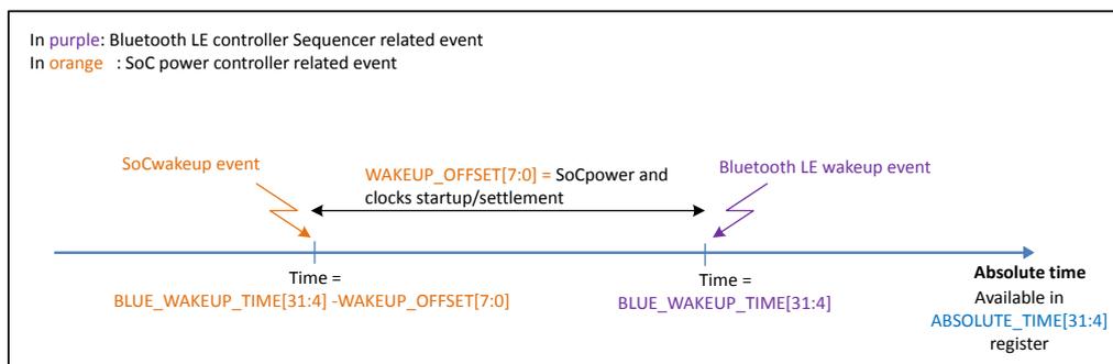
The diagram illustrates the timing contributors for an
IP_BLE
wakeup. A horizontal timeline represents 'Absolute time Available in
ABSOLUTE_TIME[31:4]
register'. Two events are marked: a 'SoC wakeup event' (orange arrow) and a 'Bluetooth LE wakeup event' (purple arrow). The time difference between them is labeled 'WAKEUP_OFFSET[7:0] = SoC power and clocks startup/settlement'. The time of the SoC wakeup event is labeled 'Time =
BLUE_WAKEUP_TIME[31:4] - WAKEUP_OFFSET[7:0]
'. The time of the Bluetooth LE wakeup event is labeled 'Time =
BLUE_WAKEUP_TIME[31:4]
'. A legend indicates: 'In purple: Bluetooth LE controller Sequencer related event' and 'In orange: SoC power controller related event'.
25.9.4 CPU wakeup management
A similar behavior is possible to generate a CPU wakeup event.
The user must program three information to activate the CPU wakeup feature:
- the
CM0_SLEEP_REQUEST_MODE[30] = CM0_WAKEUP_ENbit must be set to enable the wakeup feature, - the CPU wakeup target time in the
CM0_WAKEUP_TIME[31:4]APB register - the
WAKEUP_CM0_IRQ_ENABLE[0] = WAKEUP_ITbit must be set to have an interrupt generated on CPU on event
Note: Only the 28-bit absolute time is used for the CPU wakeup feature, so granularity of wakeup target is slow clock frequency.
In this case, the wakeup process also occurs in two steps:
- At
ABSOLUTE_TIME[31:4] = CM0_WAKEUP_TIME [31:4] - WAKEUP_OFFSET[7:0]- the wakeup block raises a SoC wakeup request towards the Power Controller of the SoC to request voltage/clock restoring.
- At
ABSOLUTE_TIME[31:4] = CM0_WAKEUP_TIME [31:4]- if
WAKEUP_CM0_IRQ_ENABLE.WAKEUP_IT = 1, the Wakeup block sends an interrupt towards the CPU (irq_wakeup_cpuline)
- if
This feature allows using the existing slow clock timer to generate a CPU wakeup source. This feature when activated has no impact on the Bluetooth LE transfers (no trigger event generated to the Bluetooth LE Sequencer).
25.9.5 wakeup block registers
The
WAKEUP_SLEEP_BLOCKBaseAddress
keyword used for all the register base address information corresponds to the wakeup registers base address decided by the SoC when integrating the IP.
Note:
WAKEUP_SLEEP_BLOCKBaseAddress
is
0x6000_1800
in
STM32WB05xZ
product.
Table 271. wakeup block register list
| Address offset | Name | RW | Reset | Description |
|---|---|---|---|---|
| 0x08 | WAKEUP_OFFSET | RW | 0x00000000 | wakeup offset register |
| 0x10 | ABSOLUTE_TIME | R | 0x00000000 | Absolute time register |
| 0x14 | MINIMUM_PERIOD_LENGTH | R | 0x00000000 | Minimum period length register |
| 0x18 | AVERAGE_PERIOD_LENGTH | R | 0x00000000 | Average period length register |
| Address offset | Name | RW | Reset | Description |
|---|---|---|---|---|
| 0x1C | MAXIMUM_PERIOD_LENGTH | R | 0x00000000 | Maximum period length register |
| 0x20 | STATISTICS_RESTART | RW | 0x00000000 | Statistics restart register |
| 0x24 | BLUE_WAKEUP_TIME | RW | 0x00000000 | IP_BLE wakeup time register |
| 0x28 | BLUE_SLEEP_REQUEST_MODE | RW | 0x00000007 | IP_BLE sleep request mode register |
| 0x2C | CM0_WAKEUP_TIME | RW | 0x00000000 | CPU wakeup time register |
| 0x30 | CM0_SLEEP_REQUEST_MODE | RW | 0x80000007 | CPU sleep request mode register |
| 0x40 | WAKEUP_BLE_IRQ_ENABLE | RW | 0x00000000 | Wakeup IP_BLE interrupt enable register |
| 0x44 | WAKEUP_BLE_IRQ_STATUS | RW | 0x00000000 | Wakeup IP_BLE interrupt status register |
| 0x48 | WAKEUP_CM0_IRQ_ENABLE | RW | 0x00000000 | Wakeup CPU interrupt enable register |
| 0x4C | WAKEUP_CM0_IRQ_STATUS | RW | 0x00000000 | Wakeup CPU interrupt status register |
25.9.5.1 Wakeup block registers
Table 272. WAKEUP_OFFSET register description
| Bit | Field name | Reset | RW | Description |
|---|---|---|---|---|
| 7:0 | WAKEUP_OFFSET | 0x0 | RW | Delay of anticipation of the Soc device to settle power and clock. Unit is in slow clock period time (typically 32 kHz). |
| 31:8 | RESERVED_31_8 | 0x0 | RW | Reserved |
Table 273. ABSOLUTE_TIME register description
| Bit | Field name | Reset | RW | Description |
|---|---|---|---|---|
| 31:0 | ABSOLUTE_TIME | 0x0 | R | Absolute time Unit of this full bit field is (slow_clock *16) frequency period cycle (typically 512 kHz). Note: ABSOLUTE_TIME[31:4] is clocked on the slow clock (typically 32 kHz), ABSOLUTE_TIME[3:0] is the interpolation at slow clock * 16 frequency (typically 512 kHz). |
Table 274. MINIMUM_PERIOD_LENGTH register description
| Bit | Field name | Reset | RW | Description |
|---|---|---|---|---|
| 3:0 | RESERVED3_0 | 0x0 | R | Reserved |
| 13:4 | LENGTH | 0x0 | R | Minimum period length computed by time interpolator |
| 31:14 | RESERVED31_14 | 0x0 | R | Reserved |
Table 275. AVERAGE_PERIOD_LENGTH register description
| Bit | Field name | Reset | RW | Description |
|---|---|---|---|---|
| 3:0 | LENGTH_FRAC | 0x0 | R | Additional information/precision on slow clock frequency. Reading AVERAGE_PERIOD_LENGTH[13:0] indicates the number of 16 MHz clock cycles contained in 16 slow clock periods. This bit field is updated every 16 slow clock periods. |
| 13:4 | LENGTH_INT | 0x0 | R | Average period length computed by Time Interpolator. This value indicates the number of 16 MHz clock cycles contained in 1 slow clock period. This bit field is updated every 16 slow clock periods. |
| 23:14 | RESERVED23_14 | 0x0 | R | Reserved |
| Bit | Field name | Reset | RW | Description |
|---|---|---|---|---|
| 31:24 | AVERAGE_COUNT | 0x0 | R | This value indicates the number of slow clock periods taken into account to calculate the average. This bit field is updated every slow clock period. This bit field is clamped at 0xFF so reading 0xFF means at least 128 slow clock periods are already being used to calculate the average. |
| Bit | Field name | Reset | RW | Description |
|---|---|---|---|---|
| 3:0 | RESERVED3_0 | 0x0 | R | Reserved |
| 13:4 | LENGTH | 0x0 | R | Maximum period length computed by Time Interpolator. |
| 31:14 | RESERVED31_14 | 0x0 | R | Reserved |
| Bit | Field name | Reset | RW | Description |
|---|---|---|---|---|
| 0 | CLR_MIN_MAX | 0x0 | RW | Write '1' to clear the minimum and maximum registers. Note: This bit is auto cleared by the hardware. |
| 1 | CLR_AVR | 0x0 | RW | Write '1' to clear the AVERAGE_PERIOD_LENGTH register value. This action clears both the average length value and the average counter. Note: This bit is auto cleared by the hardware. |
| 31:2 | RESERVED31_2 | 0x0 | R | Reserved |
| Bit | Field name | Reset | RW | Description |
|---|---|---|---|---|
| 31:0 | WAKEUP_TIME | 0x0 | RW | Programmed wakeup time for the IP_BLE. Unit is in (16 x slow clock) period so typically 512 kHz when slow clock is 32 kHz. |
| Bit | Field name | Reset | RW | Description |
|---|---|---|---|---|
| 2:0 | RESERVED2_0 | 0x7 | RW | Reserved |
| 28:3 | RESERVED28_3 | 0x0 | R | Reserved |
| 29 | SLEEP_EN | 0x0 | RW | - 0: disable IP_BLE sleeping mode = no low-power mode request when the Bluetooth LE link layer indicates it is no longer busy. - 1: enable IP_BLE sleeping mode = low-power mode request when the Bluetooth LE link layer indicates it is no longer busy. Note: Bluetooth LE Sequencer is no longer busy if no sequence is on-going and if no Timer1 nor Timer2 counter is enabled (to trig the next sequence). |
| 30 | BLE_WAKEUP_EN | 0x0 | RW | - 0: disable the IP_BLE wakeup - 1: enable the IP_BLE wakeup request through the embedded wakeup timer. This bit is auto-cleared by hardware when a wakeup event occurs (IP_BLE wakeup time matches with current time). |
| 31 | FORCE_SLEEPING | 0x0 | RW | - 0: the IP_BLE sleeping is managed dynamically according to IP_BLE activity and status - 1: the IP_BLE is always considered as sleeping, which means it always allows the SoC to go to low power mode |
| Bit | Field name | Reset | RW | Description |
|---|---|---|---|---|
| 3:0 | RESERVED3_0 | 0x0 | R | Always read as zero as no 512 kHz granularity on this time wakeup. |
| 31:4 | WAKEUP_TIME | 0x0 | RW | Programmed wakeup time for the CPU. Unit is in slow clock period. |
| Bit | Field name | Reset | RW | Description |
|---|---|---|---|---|
| 2:0 | RESERVED2_0 | 0x7 | RW | Reserved |
| 29:3 | RESERVED29_3 | 0x0 | R | Reserved |
| 30 | CPU_WAKEUP_EN | 0x0 | RW |
This bit is auto-cleared by hardware when a wakeup event occurs (CM0_WAKEUPTIME value matches with current time). |
| 31 | FORCE_SLEEPING | 0x1 | RW |
|
| Bit | Field name | Reset | RW | Description |
|---|---|---|---|---|
| 0 | WAKEUP_IT | 0x0 | RW |
|
| 31:1 | RESERVED31_1 | 0x0 | R | Reserved |
| Bit | Field name | Reset | RW | Description |
|---|---|---|---|---|
| 0 | WAKEUP_IT | 0x0 | RW | Write '1' to clear the interrupt. When read, returns the interrupt status. |
| 31:1 | RESERVED31_1 | 0x0 | R | Reserved |
| Bit | Field name | Reset | RW | Description |
|---|---|---|---|---|
| 0 | WAKEUP_IT | 0x0 | RW |
|
| 31:1 | RESERVED31_0 | 0x0 | R | Reserved |
| Bit | Field name | Reset | RW | Description |
|---|---|---|---|---|
| 0 | WAKEUP_IT | 0x0 | RW | Write '1' to clear the interrupt. When read, returns the interrupt status. |
| 31:1 | RESERVED31_0 | 0x0 | R | Reserved |