22. Universal synchronous asynchronous receiver transmitter (USART)
22.1 USART introduction
The universal synchronous asynchronous receiver transmitter (USART) offers a flexible means of full-duplex data exchange with external equipment requiring an industry standard NRZ asynchronous serial data format. The USART offers a very wide range of baud rates using a fractional baud rate generator.
It supports synchronous one-way communication and half-duplex single-wire communication. It also supports the LIN (local interconnection network), smartcard protocol and IrDA (infrared data association) SIR ENDEC specifications, and modem operations (CTS/RTS). It also supports multiprocessor communications.
High speed data communication is possible by using the DMA (direct memory access) for multi-buffer configuration.
22.2 USART main features
- • Full-duplex asynchronous communication
- • NRZ standard format (mark/space)
- • Configurable oversampling method by 16 or 8 to give flexibility between speed and clock tolerance
- • Baud rate generator systems
- • Two internal FIFOs for transmit and receive data, that can be enabled/disabled by software. FIFOs come with status flags for FIFOs states
- • A common programmable transmit and receive baud rate of up to 2 Mbit/s with the clock frequency at 16 MHz and oversampling is by 8
- • Dual clock domain with a dedicated kernel clock allowing baud rate programming independent from the PCLK reprogramming
- • Auto baud rate detection
- • Programmable data word length (7 or 8 or 9 bits)
- • Programmable data order with MSB-first or LSB-first shifting
- • Configurable stop bits (1 or 2 stop bits)
- • Synchronous master/slave mode and clock output/input for synchronous communications
- • SPI slave transmission underrun error flag
- • Single-wire half-duplex communications
- • Continuous communications using DMA
- • Received/transmitted bytes are buffered in reserved SRAM using centralized DMA
- • Separate enable bits for transmitter and receiver
- • Separate signal polarity control for transmission and reception
- • Swappable Tx/Rx pin configuration
- • Hardware flow control for modem and RS-485 transceiver
- • Communication control/error detection flags
- • Parity control:
- – Transmits parity bit
- – Checks parity of received data byte
- • Interrupt sources with flags
- • Multi processor communications
- • Wakeup from mute mode (by idle line detection or address mark detection)
22.3 USART extended features
- • LIN master synchronous break send capability and LIN slave break detection capability
- – 13-bit break generation and 10/11 bit break detection when USART is hardware configured for LIN
- • IrDA SIR encoder decoder supporting 3/16 bit duration for normal mode
- • Smartcard mode
- – Supports the T=0 and T=1 asynchronous protocols for smartcards as defined in the ISO/IEC 7816-3 standard
- – 0.5 and 1.5 stop bits for smartcard operation
- • Support for Modbus communication
- – Timeout feature
- – CR/LF character recognition
22.4 USART implementation
Table 97. USART/LPUART features describes the USART and LPUART implementation on the STM32WB05xZ device.
Table 97. USART/LPUART features
| USART modes/features (1) | USART | LPUART |
|---|---|---|
| Hardware flow control for modem | X | X |
| Continuous communication using DMA | X | X |
| Multiprocessor communication | X | X |
| Synchronous mode (master/slave) | X | - |
| Smartcard mode | X | - |
| Single-wire half-duplex communication | X | X |
| IrDA SIR ENDEC block | X | - |
| LIN mode | X | - |
| Dual clock domain | X | X |
| Receiver timeout interrupt | X | - |
| Modbus communication | X | - |
| Auto baud rate detection | X | - |
| Driver enable | X | X |
| USART data length | 7, 8 and 9 bits | |
| Tx/Rx FIFO | X | X |
| Tx/Rx FIFO size | 8 | |
1. X=supported.
22.5 USART functional description
Any USART bidirectional communication requires a minimum of two pins: receive data in (RX) and transmit data out (TX):
- •
RX:
receive data input
This is the serial data input. Oversampling techniques are used for data recovery by discriminating between valid incoming data and noise. - •
TX:
Transmit data output
When the transmitter is disabled, the output pin returns to its I/O port configuration. When the transmitter is enabled and nothing is to be transmitted, the TX pin is at high level. In single-wire and smartcard modes, this I/O is used to transmit and receive the data.
Serial data are transmitted and received through these pins in normal USART mode. The frames are comprised of:
- • An Idle Line prior to transmission or reception
- • A start bit
- • A data word (7, 8 or 9 bits) least significant bit first
- • 0.5, 1, 1.5, 2 stop bits indicating that the frame is complete
- • The USART interface uses a baud rate generator
- • A status register(USART_ISR)
- • Receive and transmit data registers (USART_RDR, USART_TDR). When FIFO mode is enabled, writing into USART_TDR adds one data to the transmit FIFO; and reading from USART_RDR removes one data from the receive FIFO
- • A baud rate register(USART_BRR)
- • A guardtime register (USART_GTPR) in case of smartcard mode.
Refer to Section 22.7: USART registers for the definitions of each bit.
The following pin is required to interface in synchronous mode and smartcard mode:
- • SCLK: This pin acts as clock output in synchronous master and smartcard modes. It acts as clock input in synchronous slave mode. In synchronous master mode, this pin outputs the transmitter data clock for synchronous transmission corresponding to SPI master mode (no clock pulses on start bit and stop bit, and a software option to send a clock pulse on the last data bit). In parallel, data can be received synchronously on RX. This can be used to control peripherals that have shift registers (e.g. LCD drivers). The clock phase and polarity are software programmable.
In smartcard mode, SCLK output can provide the clock to the smartcard.
- • NSS: This pin acts as slave select input in synchronous slave mode.
The following pins are required in RS232 hardware flow control mode:
- • nCTS: Clear to send blocks the data transmission at the end of the current transfer when high
- • nRTS: Request to send indicates that the USART is ready to receive data (when low).
The following pin is required in RS485 hardware control mode:
- • DE: driver enable activates the transmission mode of the external transceiver.
Note: DE and nRTS share the same pin.
Note: NSS and nCTS share the same pin.
Figure 124. USART block diagram![Figure 124. USART block diagram. This is a complex block diagram of a USART. At the top, there are two data registers: 'Transmit data register (TDR/TXFIFO)' and 'Receive data register (RDR/RXFIFO)'. Data is written to the TDR and read from the RDR by a CPU or DMA. Below these are 'Transmit shift register' and 'Receive shift register'. To the left is an 'IrDA SIR ENDEC block' connected to TX and RX pins. On the right is an 'SCKL control' block connected to an SCKL pin. Below the shift registers are control and configuration registers: 'USART_CR3', 'USART_CR2', 'USART_CR1', and 'USART_GTPR' (with GT and PSC fields). A 'Hardware flow controller' is connected to nRTS, /DE, and nCTS pins. Below the registers are 'Transmit control', 'Wake-up unit', and 'Receiver control' blocks. These are connected to 'USART_CR1', 'USART_ISR', and 'USART interrupt control'. At the bottom is a 'Conventional baud rate generator' containing 'USART_BRR', 'Transmitter rate controller', 'Receiver rate controller', and 'BRR[15:0]'. It is controlled by 'USART_BRR' register (TE and FE bits) and a clock divider '/USARTDIV or 2/USARTDIV (depending on the oversampling mode)'. The input clock is fCK.](/RM0529-STM32WB05xZ/5a9ea854664cdf215f6a11bda819d065_img.jpg)
Note: For details on coding USARTDIV in the USARTx_BRR register, refer to Section 22.7.4: Baud rate register (USARTx_BRR) .
Note: \( f_{CK} \) is 16 MHz.
22.5.1 USART character description
The word length can be selected as being either 7 or 8 or 9 bits by programming the M bits (M0: bit 12 and M1: bit 28) in the USART_CR1 register (see Figure 125. Word length programming ).
- • 7-bit character length: M[1:0] = 10
- • 8-bit character length: M[1:0] = 00
- • 9-bit character length: M[1:0] = 01
Note: In 7-bits data length mode, the smartcard mode, LIN master mode and auto baud rate (0x7F and 0x55 frames detection) are not supported.
In default configuration, the signal (TX or RX) is in low state during the start bit. It is in high state during the stop bit.
These values can be inverted, separately for each signal, through polarity configuration control.
An Idle character is interpreted as an entire frame of “1”s. (The number of “1”s includes the number of stop bits).
A Break character is interpreted on receiving “0”s for a frame period. At the end of the break frame, the transmitter inserts 2 stop bits.
Transmission and reception are driven by a common baud rate generator, the clock for each is generated when the enable bit is set respectively for the transmitter and receiver.
The details of each block is given below.
Figure 125. Word length programming
The diagram illustrates three word length configurations for USART communication, showing the timing of data frames, idle frames, and break frames relative to a clock signal.
- 9-bit word length (M = 01), 1 Stop bit:
- Data frame: Start bit, Bit0 through Bit8, Possible Parity bit, Stop bit, followed by the Next Start bit.
- Clock: A square wave with a note that the last data clock pulse is controlled by the LBCL bit (**).
- Idle frame: A continuous high level followed by a Start bit.
- Break frame: A continuous low level followed by two Stop bits and a Start bit.
- 8-bit word length (M = 00), 1 Stop bit:
- Data frame: Start bit, Bit0 through Bit7, Possible Parity bit, Stop bit, followed by the Next Start bit.
- Clock: Similar to the 9-bit configuration, with the last data clock pulse controlled by the LBCL bit (**).
- Idle frame: Continuous high level followed by a Start bit.
- Break frame: Continuous low level followed by two Stop bits and a Start bit.
- 7-bit word length (M = 10), 1 Stop bit:
- Data frame: Start bit, Bit0 through Bit6, Possible Parity bit, Stop bit, followed by the Next Start bit.
- Clock: Similar to the other configurations, with the last data clock pulse controlled by the LBCL bit (**).
- Idle frame: Continuous high level followed by a Start bit.
- Break frame: Continuous low level followed by two Stop bits and a Start bit.
** LBCL bit controls last data clock pulse
22.5.2 FIFOs and thresholds
The USART can operate in FIFO mode, with the FIFO buffers having a depth of 16 bytes (8 bytes TX, 8 bytes RX).
The USART comes with a transmit FIFO (TXFIFO) and a receive FIFO (RXFIFO). The FIFO mode is enabled by setting the bit 29 FIFOEN in the USARTx_CR1 register.
The FIFO mode is supported only on UART, SPI and smartcard modes.
Being 9 bits the maximum data word length, the TXFIFO is 9-bits wide. However the RXFIFO is by default 12-bits wide. This is due to the fact that the receiver does not only put the data in the FIFO, but also the error flags associated to each character (Parity error, Noise error and Framing error flags).
Note: The received data is stored in the RXFIFO with its flags. But If you read RDR, you read just the data. The status flags are available in the USART_ISR register.
It is possible to define the TXFIFO and RXFIFO levels at which the Tx and RX interrupt are triggered. These thresholds are programmed through bit fields RXFTCFG and TXFTCFG in USARTx_CR3 control register.
In this case:
- • The receive interrupt is generated when the number of received data in the RXFIFO reaches the threshold programmed in the RXFTCFG bits fields
- • The transmit interrupt is generated when the number of empty locations in the TXFIFO reaches the threshold programmed in the TXFTCFG bit fields.
RXFIFO threshold
The RXFIFO threshold is configured using the RXFTCFG bits fields in the USARTx_CR3 register.
When the number of received data is equal to the programmed RXFTCFG, the flag RXFT in the USART_ISR register is set.
Having RXFT flag set means that there are RXFTCFG data received: 1 data in USARTx_RDR and (RXFTCFG - 1) data in the RXFIFO. So, when the RXFTCFG is programmed to «101», the RXFT flag is set when 8 data are received: 7 data in the RXFIFO and 1 data in the USARTx_RDR. Consequently, the 9 th received data do not set the overrun flag.
22.5.3 Transmitter
The transmitter can send data words of either 7 or 8 or 9 bits depending on the M bit status. The transmit enable bit (TE) must be set in order to activate the transmitter function. The data in the transmit shift register is output on the TX pin and the corresponding clock pulses are output on the SCLK pin.
Character transmission
During an USART transmission, data shifts out least significant bit first (default configuration) on the TX pin. In this mode, the USARTx_TDR register consists of a buffer (TDR) between the internal bus and the transmit shift register.
When FIFO mode is enabled, data written to the transmit data register USART_TDR, is queued in the TXFIFO.
Every character is preceded by a start bit which is a logic level low for one bit period. The character is terminated by a configurable number of stop bits.
The following stop bits are supported by USART: 0.5, 1, 1.5 and 2 stop bits.
Note: The TE bit must be set before writing the data to be transmitted to the USART_TDR. The TE bit should not be reset during transmission of data. Resetting the TE bit during the transmission corrupts the data on the TX pin as the baud rate counters get frozen. The current data being transmitted are lost. An idle frame is sent after the TE bit is enabled.
Configurable stop bits
The number of stop bits to be transmitted with every character can be programmed in control register 2, bits 13,12.
- • 1 stop bit: this is the default value of number of stop bits
- • 2 stop bits: this is supported by normal USART, single-wire and modem modes
- • 1.5 stop bits: to be used in smartcard mode.
An idle frame transmission includes the stop bits.
A break transmission is 10 low bits (when M[1:0] = 00) or 11 low bits (when M[1:0] = 01) or 9 low bits (when M[1:0] = 10) followed by 2 stop bits (see Figure 126. Configurable stop bits ). It is not possible to transmit long breaks (break of length greater than 9/10/11 low bits).
Figure 126. Configurable stop bits
The diagram illustrates three timing scenarios for 8-bit data transmission, showing the relationship between the data frame, stop bits, and the next data frame relative to a CLOCK signal.
- 8-bit data, 1 Stop bit: The sequence starts with a Start bit, followed by an 8-bit Data frame (Bit0 to Bit7), a Possible parity bit, a single Stop bit, and then the Next start bit for the next data frame. A CLOCK signal is shown below the bits, with a note that the ** LBCL bit controls the last data clock pulse.
- 8-bit data, 1 1/2 Stop bits: The sequence starts with a Start bit, followed by an 8-bit Data frame (Bit0 to Bit7), a Possible parity bit, 1.5 Stop bits, and then the Next start bit for the next data frame.
- 8-bit data, 2 Stop bits: The sequence starts with a Start bit, followed by an 8-bit Data frame (Bit0 to Bit7), a Possible parity bit, 2 Stop bits, and then the Next start bit for the next data frame.
Character transmission procedure
- 1. Program the M bits in USART_CR1 to define the word length.
- 2. Select the desired baud rate using the USART_BRR register.
- 3. Program the number of stop bits in USART_CR2.
- 4. Enable the USART by writing the UE bit in USART_CR1 register to 1.
- 5. Select DMA enable (DMAT) in USART_CR3 if multi-buffer communication is to take place. Configure the DMA register as explained in multi-buffer communication.
- 6. Set the TE bit in USART_CR1 to send an idle frame as first transmission.
- 7. Write the data to send in the USART_TDR register. Repeat this for each data to be transmitted in case of single buffer.
- a. When FIFO mode is disabled, writing a data in the USART_TDR clears the TXE flag.
- b. When FIFO mode is enabled, writing a data in the USART_TDR adds one data to the TXFIFO and write operations in the USART_TDR are made when TXFNF flag is set. This flag remains set until the TXFIFO is full.
- 8. After writing the last data into the USART_TDR register, wait until TC=1.
- – When FIFO mode is disabled, this indicates that the transmission of the last frame is complete.
- – When FIFO mode is enabled, this indicates that both TXFIFO and shift register are empty.
Single byte communication
- • When FIFO mode is disabled:
clearing the TXE flag is always performed by a write to the transmit data register. The TXE flag is set by hardware and it indicates:
- • the data has been moved from the USARTx_TDR register to the shift register and the data transmission has started
- • the USARTx_TDR register is empty
- • the next data can be written in the USARTx_TDR register without overwriting the previous data.
This flag generates an interrupt if the TXEIE bit is set.
When a transmission is taking place, a write instruction to the USARTx_TDR register stores the data in the TDR register and which is copied in the shift register at the end of the current transmission.
When no transmission is taking place, a write instruction to the USARTx_TDR register places the data in the shift register, the data transmission starts, and the TXE bit is set.
- • When FIFO mode is enabled, the TXFNF (TXFIFO not full) flag is set by hardware and it indicates:
- – the TXFIFO is not full
- – the USART_TDR register is empty
- – the next data can be written in the USART_TDR register without overwriting the previous data. When a transmission is taking place, a write operation to the USART_TDR register stores the data in the TXFIFO. Data are copied from the TXFIFO into the shift register at the end of the current transmission.
When the TXFIFO is not full, the TXFNF flag stays at 1 even after a write in USART_TDR . It is cleared when the TXFIFO is full.
This flag generates an interrupt if the TXFNFIE bit is set.
Alternatively, interrupts can be generated and data can be written into FIFO when the TXFIFO threshold is reached. In this case, the CPU can write a block of data defined by the programmed trigger level.
If a frame is transmitted (after the stop bit) and the TXE flag (TXFE in case of FIFO mode) is set, the TC flag goes high. An interrupt is generated if the TCIE bit is set in the USART_CR1 register.
After writing the last data in the USART_TDR register, it is mandatory to wait for TC=1 before disabling the USART or causing the microcontroller to enter the low-power mode (see Figure 127. TC/TXE behavior when transmitting ).
Figure 127. TC/TXE behavior when transmitting
The diagram illustrates the sequence of events for transmitting three frames (F1, F2, F3) after an idle preamble. The signals shown are the TX line, TXE flag, USART_DR, and TC flag.
- TX line: Shows an idle preamble followed by the transmission of Frame 1, Frame 2, and Frame 3.
- TXE flag:
- Initially high.
- When F1 is written to USART_DR, TXE is set by hardware.
- TXE is cleared by software when it is read.
- When F2 is written to USART_DR, TXE is set by hardware.
- TXE is cleared by software when it is read.
- When F3 is written to USART_DR, TXE is set by hardware.
- TXE remains set until the transmission of F3 is complete.
- USART_DR: Shows the data registers being loaded with F1, F2, and F3.
- TC flag:
- Initially high.
- When F1 is written, TC is not set because TXE=0.
- When F2 is written, TC is not set because TXE=0.
- When F3 is written, TC is not set because TXE=0.
- TC is set by hardware when TXE=1 and the transmission of F3 is complete.
Software logic:
- Software enables the USART.
- Software waits until TXE=1 and writes F1 into DR.
- Software waits until TXE=1 and writes F2 into DR.
- Software waits until TXE=1 and writes F3 into DR.
- Software waits until TC=1.
Note: When FIFO management is enabled, the TXFNF flag is used for data transmission.
Break characters
Setting the SBKRQ bit transmits a break character. The break frame length depends on the M bit (see Figure 125. Word length programming).
If a '1' is written to the SBKRQ bit, a break character is sent on the TX line after completing the current character transmission. The SBKF bit is set by the write operation and it is reset by hardware when the break character is completed (during the stop bits after the break character). The USART inserts a logic 1 signal (STOP) for the duration of 2 bits at the end of the break frame to guarantee the recognition of the start bit of the next frame.
When the SBKRQ bit is set, the break character is sent at the end of the current transmission.
When FIFO mode is enabled, sending the break character has priority on sending data even if the TXFIFO is full.
Idle characters
Setting the TE bit drives the USART to send an idle frame before the first data frame.
22.5.4 Receiver
The USART can receive data words of either 7 or 8 or 9 bits depending on the M bits in the USART_CR1 register.
Start bit detection
The start bit detection sequence is the same when oversampling by 16 or by 8. In the USART, the start bit is detected when a specific sequence of samples is recognized. This sequence is: 1 1 1 0 X 0 X 0 X 0 X 0 X 0.
Figure 128. Start bit detection when oversampling by 16 or 8
The diagram illustrates the start bit detection process. The RX line transitions from Idle to a Start bit (low). Ideal sample clocks are shown as regular pulses. Real sample clocks are shown as pulses that are shifted relative to the ideal ones. The sampled values are shown as a sequence of bits: 1 1 1 0 X 0 X 0 X 0 X 0 X 0. The first three samples (1 1 1) are used for falling edge detection. The subsequent samples (0 X, 0 X, 0 X) are used to verify that at least 2 bits out of 3 are at 0. The duration of one bit time is indicated as 7/16 of the ideal sample clock period. The 6/16 and 7/16 durations are also shown for the start bit detection sequence.
Note: If the sequence is not complete, the start bit detection aborts and the receiver returns to the idle state (no flag is set), where it waits for a falling edge.
The start bit is confirmed (RXNE flag set, interrupt generated if RXNEIE=1 (RXFNE flag set, interrupt generated if RXFNEIE=1 if FIFO mode is enabled) if the 3 sampled bits are at 0 (first sampling on the 3rd, 5th and 7th bits finds the 3 bits at 0 and second sampling on the 8th, 9th and 10th bits also finds the 3 bits at 0).
The start bit is validated but the NF noise flag is set if,
- 1. for both samplings, 2 out of the 3 sampled bits are at 0 (sampling on the 3rd, 5th and 7th bits and sampling on the 8th, 9th and 10th bits)
or - 2. for one of the samplings (sampling on the 3rd, 5th and 7th bits or sampling on the 8th, 9th and 10th bits), 2 out of the 3 bits are found at 0.
If neither conditions, 1 or 2, are met, the start detection aborts and the receiver returns to the idle state (no flag is set).
Character reception
During a USART reception, data shifts in least significant bit first (default configuration) through the RX pin.
Character reception procedure
- 1. Program the M bits in USART_CR1 to define the word length
- 2. Select the desired baud rate using the baud rate register USART_BRR
- 3. Program the number of stop bits in USART_CR2
- 4. Enable the USART by writing the UE bit in USART_CR1 register to 1
- 5. Select DMA enable (DMAR) in USART_CR3 if multi-buffer communication is to take place. Configure the DMA register as explained in multi-buffer communication
- 6. Set the RE bit USART_CR1. This enables the receiver which begins searching for a start bit.
When a character is received
- • When FIFO mode is disabled, the RXNE bit is set indicating that the content of the shift register is transferred to the RDR. In other words, data has been received and can be read (as well as its associated error flags)
- • When FIFO is enabled, the RXFNE bit is set indicating that the RXFIFO is not empty. A read of the USART_RDR gets the oldest entry in the RXFIFO. When a data is received, it is stored in the RXFIFO, with error bits associated with that data
- • An interrupt is generated if the RXNEIE (RXFNEIE in case of FIFO mode) bit is set
- • The error flags can be set if a frame error, noise, parity or an overrun error has been detected during reception
- • In multi-buffer communication:
- – When FIFO mode is disabled, the RXNE is set after every byte received and is cleared by the DMA read of the receive data register.
- – When FIFO mode is enabled, the RXFNE is set when the RXFIFO is not empty. After every DMA request, a data is retrieved from the RXFIFO. DMA request is triggered by RXFIFO if not empty, i.e. there is data in the RXFIFO to be read.
- • In single buffer mode,
- – When FIFO mode is disabled: clearing the RXNE flag is performed by a software read to the USARTx_RDR register. The RXNE flag can also be cleared by writing 1 to the RXFRQ in the USARTx_RQR register. The RXNE flag must be cleared before the end of the reception of the next character to avoid an overrun error.
- – When FIFO mode is enabled, the RXFNE is set when the RXFIFO is not empty. After every read of the USART_RDR, a data is retrieved from the RXFIFO. When the RXFIFO is empty, the RXFNE flag is cleared. The RXFNE flag can also be cleared by writing 1 to the RXFRQ in the USART_RQR register. When the RXFIFO is full, the first entry in the RXFIFO must be read before the end of the reception of the next character to avoid an overrun error. The RXFNE flag generates an interrupt if the RXFNEIE bit is set. Alternatively, interrupts can be generated and data can be read from RXFIFO when the RXFIFO threshold is reached. In this case, the CPU can read a block of data defined by the programmed threshold.
Break character
When a break character is received, the USART handles it as a framing error.
Idle character
When an idle frame is detected, there is the same procedure as for a received data character plus an interrupt if the IDLEIE bit is set.
Overrun error
- • FIFO mode disabled:
An overrun error occurs when a character is received when RXNE has not been reset. Data cannot be transferred from the shift register to the RDR register until the RXNE bit is cleared. The RXNE flag is set after every byte received. An overrun error occurs if RXNE flag is set when the next data is received or the previous DMA request has not been serviced. When an overrun error occurs:
- 1. The ORE bit is set.
- 2. The RDR content is not lost. The previous data is available when a read to USARTx_RDR is performed.
- 3. The shift register is overwritten. After that point, any data received during overrun is lost.
- 4. An interrupt is generated if either the RXNEIE bit is set or EIE bit is set.
- • FIFO mode enabled
An overrun error occurs when the shift register is ready to be transferred when the receive FIFO is full. Data can not be transferred from the shift register to the USARTx_RDR register until there is one free location in the RXFIFO. The RXFNE flag is set when the RXFIFO is not empty. An overrun error occurs if the RXFIFO is full and the shift register is ready to be transferred. When an overrun error occurs:
- 1. The ORE bit is set.
- 2. The first entry in the RXFIFO is not lost. It is available when a read to USART_RDR is performed.
- 3. The shift register is overwritten. After that point, any data received during overrun is lost.
- 4. An interrupt is generated if either the RXFNEIE bit is set or EIE bit is set.
The ORE bit is reset by setting the ORECF bit in the USARTx_ICR register.
Note: The ORE bit, when set, indicates that at least 1 data has been lost. When the FIFO mode is disabled, there are two possibilities
- • if RXNE=1, then the last valid data is stored in the receive register RDR and can be read
- • if RXNE=0, then it means that the last valid data has already been read and thus there is nothing to be read in the RDR. This case can occur when the last valid data is read in the RDR at the same time as the new (and lost) data is received.
Selecting the clock source and the proper oversampling method
The clock source frequency is \( f_{CK} \) (16 MHz).
The \( f_{CK} \) can be divided by a programmable factor in the USARTx_PRESC register.
Figure 129. usart_ker_ck clock divider block diagram
![Block diagram of the usart_ker_ck clock divider. An input signal 'usart_ker_ck' enters a grey box. Inside the box, it first passes through a block labeled 'USARTx_PRESC[3:0]'. The output of this block, labeled 'usart_ker_ck_pres', then enters another block labeled 'USARTx_BRR register and oversampling'.](/RM0529-STM32WB05xZ/9cb749c8c85bf7890745e0856c6d352e_img.jpg)
MSv40855V1
The communication speed range (specially the maximum communication speed) is also determined by the clock source.
The receiver implements different user-configurable oversampling techniques (except in synchronous mode) for data recovery by discriminating between valid incoming data and noise. This allows a trade off between the maximum communication speed and noise/clock inaccuracy immunity.
The oversampling method can be selected by programming the OVER8 bit in the USART_CR1 register and can be either 16 or 8 times the baud rate clock (Figure 130. Data sampling when oversampling by 16 and Figure 131. Data sampling when oversampling by 8).
Depending on the application:
- • Select oversampling by 8 (OVER8=1) to achieve higher speed (up to \( f_{CKPRES}/8 \) ). In this case the maximum receiver tolerance to clock deviation is reduced (refer to Section 22.5.6: Tolerance of the USART receiver to clock deviation).
- • Select oversampling by 16 (OVER8=0) to increase the tolerance of the receiver to clock deviations. In this case, the maximum speed is limited to maximum \( f_{CKPRES}/16 \) .
where \( f_{CKPRES} \) is the USART input clock divided by a prescaler.
Programming the ONEBIT bit in the USART_CR3 register selects the method used to evaluate the logic level. There are two options:
- • The majority vote of the three samples in the center of the received bit. In this case, when the 3 samples used for the majority vote are not equal, the NF bit is set
- • A single sample in the center of the received bit
Depending on the application:- – select the three samples' majority vote method (ONEBIT=0) when operating in a noisy environment and reject the data when a noise is detected (refer to Figure 2 because this indicates that a glitch occurred during the sampling).
- – select the single sample method (ONEBIT=1) when the line is noise-free to increase the receiver's tolerance to clock deviations (see Section 22.5.6: Tolerance of the USART receiver to clock deviation). In this case the NF bit is never set.
When noise is detected in a frame:
- • The NF bit is set at the rising edge of the RXNE bit (RXFNE in case of FIFO mode enabled)
- • The invalid data is transferred from the Shift register to the USART_RDR register
- No interrupt is generated in case of single byte communication. However this bit rises at the same time as the RXNE bit (RXFNE in case of FIFO mode enabled) which itself generates an interrupt. In case of multi-buffer communication an interrupt is issued if the EIE bit is set in the USART_CR3 register.
The NF bit is reset by setting NFCF bit in the ICR register.
Note: Noise error is not supported in SPI mode.
Note: Oversampling by 8 is not available in the smartcard, IrDA and LIN modes. In those modes, the OVER8 bit is forced to '0' by hardware.
Figure 130. Data sampling when oversampling by 16
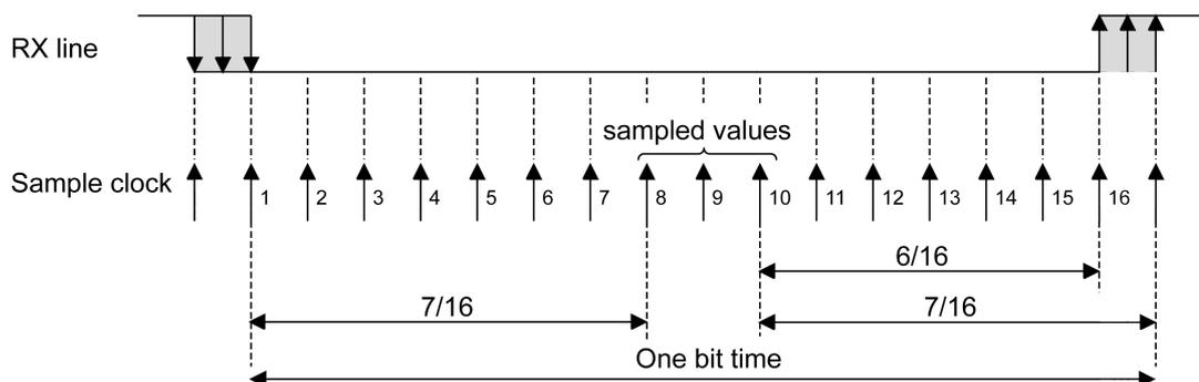
Figure 131. Data sampling when oversampling by 8
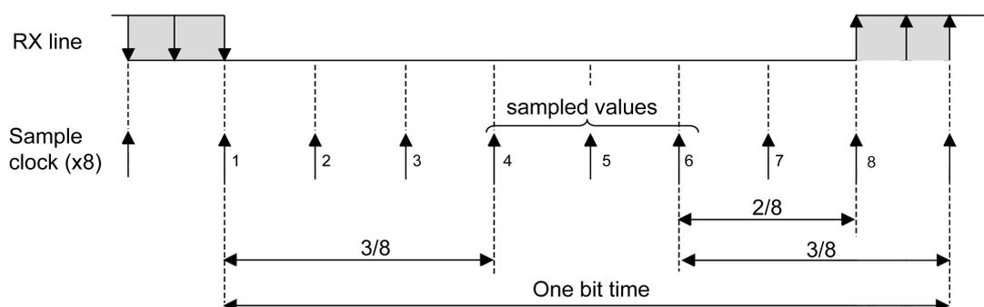
Table 98. Noise detection from sampled data
| Sampled value | NE status | Received bit value |
|---|---|---|
| 000 | 0 | 0 |
| 001 | 1 | 0 |
| 010 | 1 | 0 |
| 011 | 1 | 1 |
| 100 | 1 | 0 |
| 101 | 1 | 1 |
| 110 | 1 | 1 |
| 111 | 0 | 1 |
Framing error
A framing error is detected when the stop bit is not recognized on reception at the expected time, following either a de-synchronization or excessive noise.
When the framing error is detected:
- The FE bit is set by hardware
- The invalid data is transferred from the shift register to the USART_RDR register ( RXFIFO in case FIFO mode is enabled)
- No interrupt is generated in case of single byte communication. However this bit rises at the same time as the RXNE bit (RXFNE in case FIFO mode is enabled) which itself generates an interrupt. In case of multi-buffer communication an interrupt is issued if the EIE bit is set in the USART_CR3 register.
The FE bit is reset by writing 1 to the FECF in the USART_ICR register.
Note: Framing error is not supported in SPI mode.
Configurable stop bits during reception
The number of stop bits to be received can be configured through the control bits of control register 2 - it can be either 1 or 2 in normal mode and 0.5 or 1.5 in smartcard mode.
- 0.5 stop bit (reception in smartcard mode): No sampling is done for 0.5 stop bit. As a consequence, no framing error and no break frame can be detected when 0.5 stop bit is selected.
- 1 stop bit: Sampling for 1 stop bit is done on the 8 th , 9 th and 10 th samples.
- 1.5 stop bits (smartcard mode): When transmitting in smartcard mode, the device must check that the data is correctly sent. Thus the receiver block must be enabled (RE=1 in the USART_CR1 register) and the stop bit is checked to test if the smartcard has detected a parity error. In the event of a parity error, the smartcard forces the data signal low during the sampling - NACK signal -, which is flagged as a framing error. Then, the FE flag is set with the RXNE (RXFNE in case FIFO mode is enabled) at the end of the 1.5 stop bit. Sampling for 1.5 stop bits is done on the 16 th , 17 th and 18 th samples (1 baud clock period after the beginning of the stop bit). The 1.5 stop bit can be decomposed into 2 parts: one 0.5 baud clock period during which nothing happens, followed by 1 normal stop bit period during which sampling occurs halfway through. Refer to Section 22.5.14: Receiver timeout for more details.
- 2 stop bits: Sampling for 2 stop bits is done on the 8 th , 9 th and 10 th samples of the first stop bit. If a framing error is detected during the first stop bit the framing error flag is set. The second stop bit is not checked for framing error. The RXNE (RXFNE in case FIFO mode is enabled) flag is set at the end of the first stop bit.
22.5.5 Baud rate generation
The baud rate for the receiver and transmitter (Rx and Tx) are both set to the same value as programmed in the USART_BRR register.
Equation 1: Baud rate for standard USART (SPI mode included) (OVER8 = 0 or 1).
In case of oversampling by 16, the equation is:
In case of oversampling by 8, the equation is:
Equation 2: Baud rate in Smartcard, LIN and IrDA modes (OVER8 = 0)
\( f_{CKPRES} \) is the USART clock which is the USART input clock divided by a prescaler configured in the USART_PRES register.
USARTDIV is an unsigned fixed point number that is coded on the USART_BRR register.
- When OVER8 = 0, BRR = USARTDIV
- When OVER8 = 1
- BRR[2:0] = USARTDIV[3:0] shifted 1 bit to the right
- BRR[3] must be kept cleared
- BRR[15:4] = USARTDIV[15:4]
Note: The baud counters are updated to the new value in the baud registers after a write operation to USART_BRR. Hence the baud rate register value should not be changed during communication. In case of oversampling by 16 and 8, USARTDIV must be greater than or equal to 16d.
How to derive USARTDIV from USART_BRR register values
Example 1
To obtain 9600 baud with \( f_{CKPRES} = 8 \) MHz.
- • In case of oversampling by 16:
\( USARTDIV = 8\,000\,000/9600 \)
\( BRR = USARTDIV = 833d = 0341h \) - • In case of oversampling by 8:
\( USARTDIV = 2 * 8\,000\,000/9600 \)
\( USARTDIV = 1666,66 \) ( \( 1667d = 683h \) )
\( BRR[3:0] = 3h \gg 1 = 1h \)
\( BRR = 0x681 \)
22.5.6 Tolerance of the USART receiver to clock deviation
The asynchronous receiver of the USART works correctly only if the total clock system deviation is less than the tolerance of the USART receiver. The causes which contribute to the total deviation are:
- • DTRA: Deviation due to the transmitter error (which also includes the deviation of the transmitter's local oscillator)
- • DQUANT: Error due to the baud rate quantization of the receiver
- • DREC: Deviation of the receiver local oscillator
- • DTCL: Deviation due to the transmission line (generally due to the transceivers which can introduce an asymmetry between the low-to-high transition timing and the high-to-low transition timing)
\( DTRA + DQUANT + DREC + DTCL < USART receiver tolerance \) .
The USART receiver can receive data correctly at up to the maximum tolerated deviation specified in Table 99. Tolerance of the USART receiver when BRR [3:0] = 0000 (high-density devices) and Table 100. Tolerance of the USART receiver when BRR[3:0] is different from 0000 (high-density devices) , depending on the following choices:
- • 9-,10- or 11-bit character length defined by the M bits in the USART_CR1 register
- • Oversampling by 8 or 16 defined by the OVER8 bit in the USART_CR1 register
- • Bits BRR[3:0] of USART_BRR register are equal to or different from 0000
- • Use of 1 bit or 3 bits to sample the data, depending on the value of the ONEBIT bit in the USART_CR3 register.
Table 99. Tolerance of the USART receiver when BRR [3:0] = 0000 (high-density devices)
| M bits | OVER8 bit = 0 | OVER8 bit = 1 | ||
|---|---|---|---|---|
| ONEBIT=0 | ONEBIT=1 | ONEBIT=0 | ONEBIT=1 | |
| 00 | 3.75% | 4.375% | 2.50% | 3.75% |
| 01 | 3.41% | 3.97% | 2.27% | 3.41% |
| 10 | 4.16 | 4.86 | 2.77 | 4.16 |
Table 100. Tolerance of the USART receiver when BRR[3:0] is different from 0000 (high-density devices)
| M bits | OVER8 bit = 0 | OVER8 bit = 1 | ||
|---|---|---|---|---|
| ONEBIT=0 | ONEBIT=1 | ONEBIT=0 | ONEBIT=1 | |
| 00 | 3.33% | 3.88% | 2% | 3% |
| 01 | 3.03% | 3.53% | 1.82% | 2.73% |
| 10 | 3.7 | 4.31 | 2.22 | 3.33 |
Note: The data specified in Table 99. Tolerance of the USART receiver when BRR [3:0] = 0000 (high-density devices) and Table 100. Tolerance of the USART receiver when BRR[3:0] is different from 0000 (high-density devices) may slightly differ in the special case when the received frames contain some Idle frames of exactly 10-bit times when M bits = 00 (11-bit times when M = 01 or 9-bit times when M = 10).
22.5.7 Auto baud rate detection
The USART is able to detect and automatically set the USART_BRR register value based on the reception of one character. Automatic baud rate detection is useful under two circumstances:
- • The communication speed of the system is not known in advance
- • The system is using a relatively low accuracy clock source and this mechanism allows the correct baud rate to be obtained without measuring the clock deviation.
The clock source frequency must be compatible with the expected communication speed (when oversampling by 16, the baud rate is between \( f_{CK}/65535 \) and \( f_{CK}/16 \) . When oversampling by 8, the baud rate is between \( f_{CK}/65535 \) and \( f_{CK}/8 \) .
Before activating the auto baud rate detection, the auto baud rate detection mode must be chosen. There are four modes based on different character patterns.
The modes can be chosen through the ABRMOD[1:0] field in the USART_CR2 register. In these auto baud rate modes, the baud rate is measured several times during the synchronization data reception and each measurement is compared to the previous one.
These modes are:
- •
Mode 0:
Any character starting with a bit at 1.
In this case the USART measures the duration of the start bit (falling edge to rising edge). - •
Mode 1:
Any character starting with a 10xx bit pattern.
In this case, the USART measures the duration of the start and of the 1 st data bit. The measurement is done falling edge to falling edge, ensuring better accuracy in the case of slow signal slopes. - •
Mode 2:
A 0x7F character frame (it may be a 0x7F character in LSB first mode or a 0xFE in MSB first mode).
In this case, the baud rate is updated first at the end of the start bit (BRs), then at the end of bit 6 (based on the measurement done from falling edge to falling edge: BR6). Bit0 to Bit6 are sampled at BRs while further bits of the character are sampled at BR6. - •
Mode 3:
A 0x55 character frame.
In this case, the baud rate is updated first at the end of the start bit (BRs), then at the end of bit0 (based on the measurement done from falling edge to falling edge: BR0), and finally at the end of bit6 (BR6). Bit0 is sampled at BRs, Bit1 to Bit6 are sampled at BR0, and further bits of the character are sampled at BR6. In parallel, another check is performed for each intermediate transition of RX line. An error is generated if the transitions on RX are not sufficiently synchronized with the receiver (the receiver being based on the baud rate calculated on bit 0).
Prior to activating auto baud rate detection, the USART_BRR register must be initialized by writing a non-zero baud rate value.
The automatic baud rate detection is activated by setting the ABREN bit in the USART_CR2 register. The USART then waits for the first character on the RX line. The auto baud rate operation completion is indicated by the setting of the ABRF flag in the USART_ISR register. If the line is noisy, the correct baud rate detection cannot be guaranteed. In this case the BRR value may be corrupted and the ABRE error flag is set. This also happens if the communication speed is not compatible with the automatic baud rate detection range (bit duration not between 16 and 65536 clock periods (oversampling by 16) and not between 8 and 65536 clock periods (oversampling by 8)).
The auto baud rate detection can be re-launched later by resetting the ABRF flag (by writing a 0).
When FIFO management is disabled, in case of auto baud rate error, the ABRE flag is set with RXNE and FE.
When FIFO management is enabled, in case of auto baud rate error, the ABRE flag is set with RXFNE and FE.
In case FIFO mode is enabled, the auto baud rate detection should be made using the data on the first RXFIFO location. So, prior to launching the auto baud rate detection, the user should make sure that the RXFIFO is empty using the RXFNE flag in the USARTx_ISR register.
Note: The BRR value may be corrupted if the USART is disabled (UE=0) during an auto baud rate operation.
22.5.8 Multiprocessor communication
It is possible to perform multiprocessor communication with the USART (with several USARTs connected in a network). For instance one of the USARTs can be the master, its TX output connected to the RX inputs of the other USARTs. The others are slaves, their respective TX outputs are logically ANDed together and connected to the RX input of the master.
In multiprocessor configurations it is often desirable that only the intended message recipients should actively receive the full message contents, thus reducing redundant USART service overhead for all non addressed receivers.
The non addressed devices may be placed in mute mode by means of the muting function. In order to use the mute mode feature, the MME bit must be set in the USARTx_CR1 register.
Note: When FIFO management is enabled and MME is already set, MME bit must not be cleared and then set again quickly (within two UCLK cycles) otherwise mute mode might remain active.
In mute mode:
- • None of the reception status bits can be set
- • All the receive interrupts are inhibited
- • The RWU bit in USART_ISR register is set to 1. RWU can be controlled automatically by hardware or by software, through the MMRQ bit in the USART_RQR register, under certain conditions.
The USART can enter or exit from mute mode using one of two methods, depending on the WAKE bit in the USART_CR1 register:
- • Idle Line detection if the WAKE bit is reset
- • Address Mark detection if the WAKE bit is set.
Idle line detection (WAKE=0)
The USART enters mute mode when the MMRQ bit is written to 1 and the RWU is automatically set. It wakes up when an idle frame is detected. Then the RWU bit is cleared by hardware but the IDLE bit is not set in the USART_ISR register. An example of mute mode behavior using Idle line detection is given in Figure 132. Mute mode using Idle line detection.
Figure 132. Mute mode using Idle line detection
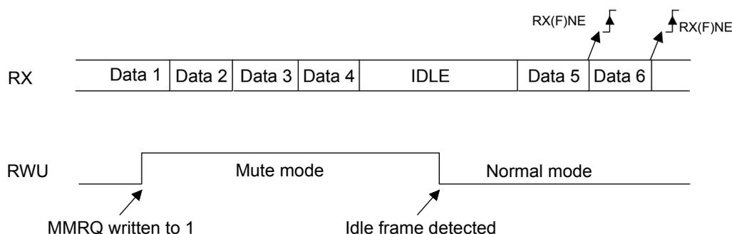
The diagram illustrates the relationship between the RX line and the RWU signal during mute mode operation using idle line detection. The RX line shows a sequence of data frames: Data 1, Data 2, Data 3, Data 4, followed by an IDLE period, then Data 5, and Data 6. RX(F)NE (Receive Frame Not Empty) pulses are shown at the beginning of Data 5 and Data 6. The RWU signal starts low, transitions to high when 'MMRQ written to 1', entering 'Mute mode', and transitions back to low when 'Idle frame detected', returning to 'Normal mode'.
Note: If the MMRQ is set while the IDLE character has already elapsed, mute mode is not entered (RWU is not set).
Note: If the USART is activated while the line is IDLE, the idle state is detected after the duration of one IDLE frame (not only after the reception of one character frame).
4-bit/7-bit address mark detection (WAKE=1)
In this mode, bytes are recognized as addresses if their MSB is a '1' otherwise they are considered as data. In an address byte, the address of the targeted receiver is put in the 4 or 7 LSBs. The choice of 7 or 4 bit address detection is done using the ADDM7 bit. This 4-bit/7-bit word is compared by the receiver with its own address which is programmed in the ADD bits in the USART_CR2 register.
Note: In 7-bit and 9-bit data modes, address detection is done on 6-bit and 8-bit addresses (ADD[5:0] and ADD[7:0]) respectively.
The USART enters mute mode when an address character is received which does not match its programmed address. In this case, the RWU bit is set by hardware. The RXNE flag is not set for this address byte and no interrupt or DMA request is issued when the USART enters mute mode. When FIFO management is enabled, the software should ensure that there is at least one empty location in the RXFIFO before entering mute mode.
The USART also enters mute mode when the MMRQ bit is written to 1. The RWU bit is also automatically set in this case. The USART exits from mute mode when an address character is received which matches the programmed address. Then the RWU bit is cleared and subsequent bytes are received normally. The RXNE/RXFNE bit is set for the address character since the RWU bit has been cleared.
Note: When FIFO management is enabled, when MMRQ is set while the receiver is sampling the last bit of data, these data maybe be received before entering mute mode.
An example of mute mode behavior using address mark detection is given in Figure 133. Mute mode using address mark detection.
Figure 133. Mute mode using address mark detection
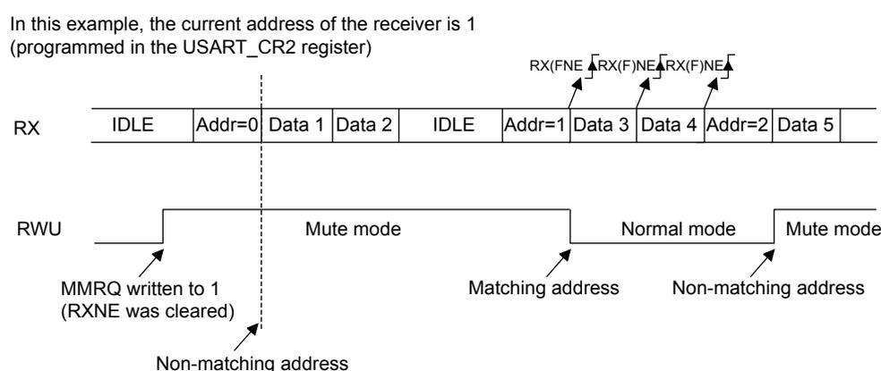
In this example, the current address of the receiver is 1 (programmed in the USART_CR2 register)
The diagram illustrates the RX and RWU signals during address mark detection. The RX signal shows a sequence of IDLE, Addr=0, Data 1, Data 2, IDLE, Addr=1, Data 3, Data 4, Addr=2, Data 5. The RWU signal shows transitions between Mute mode and Normal mode. Mute mode is entered when Addr=0 (non-matching) and Addr=2 (non-matching) are received. Normal mode is entered when Addr=1 (matching) is received. RX(F)NE flags are shown for the matching address characters.
Key events shown in the diagram:
- MMRQ written to 1 (RXNE was cleared): The initial transition to Mute mode.
- Non-matching address (Addr=0): The USART enters Mute mode.
- Matching address (Addr=1): The USART exits Mute mode and enters Normal mode. The RX(F)NE flag is set.
- Non-matching address (Addr=2): The USART enters Mute mode again.
22.5.9 Modbus communication
The USART offers basic support for the implementation of Modbus/RTU and Modbus/ASCII protocols.
Modbus/RTU is a half-duplex, block transfer protocol. The control part of the protocol (address recognition, block integrity control and command interpretation) must be implemented in software.
The USART offers basic support for the end of the block detection, without software overhead or other resources.
Modbus/RTU
In this mode, the end of one block is recognized by a “silence” (idle line) for more than 2 character times. This function is implemented through the programmable timeout function.
The timeout function and interrupt must be activated, through the RTOEN bit in the USART_CR2 register and the RTOIE in the USART_CR1 register. The value corresponding to a timeout of 2 character times (for example 22 x bit time) must be programmed in the RTO register. When the receive line is idle for this duration, after the last stop bit is received, an interrupt is generated, informing the software that the current block reception is completed.
Modbus/ASCII
In this mode, the end of a block is recognized by a specific (CR/LF) character sequence. The USART manages this mechanism using the character match function. By programming the LF ASCII code in the ADD[7:0] field and by activating the character match interrupt (CMIE=1), the software is informed when an LF has been received and can check the CR/LF in the DMA buffer.
22.5.10 Parity control
Parity control (generation of parity bit in transmission and parity checking in reception) can be enabled by setting the PCE bit in the USART_CR1 register. Depending on the frame length defined by the M bits, the possible USART frame formats are as listed in Table 101. Frame formats .
Table 101. Frame formats
| M bits | PCE bit | USART frame (1) |
|---|---|---|
| 00 | 0 | | SB | 8-bit data | STB | |
| 00 | 1 | | SB | 7-bit data | PB | STB | |
| 01 | 0 | | SB | 9-bit data | STB | |
| 01 | 1 | | SB | 8-bit data PB | STB | |
| 10 | 0 | | SB | 7-bit data | STB | |
| 10 | 1 | | SB | 6-bit data | PB | STB | |
1. Legends: SB: start bit, STB: stop bit, PB: parity bit. In the data register, the PB is always taking the MSB position (8 th or 7 th , depending on the M bit value).
Even parity
The parity bit is calculated to obtain an even number of “1s” inside the frame of the 6, 7 or 8 LSB bits (depending on M bit values) and the parity bit.
As an example, if data=00110101, and 4 bits are set, then the parity bit is 0 if even parity is selected (PS bit in USART_CR1 = 0).
Odd parity
The parity bit is calculated to obtain an odd number of “1s” inside the frame made of the 6, 7 or 8 LSB bits (depending on M bit values) and the parity bit.
As an example, if data=00110101 and 4 bits set, then the parity bit is 1 if odd parity is selected (PS bit in USART_CR1 = 1).
Parity checking in reception
If the parity check fails, the PE flag is set in the USART_ISR register and an interrupt is generated if PEIE is set in the USART_CR1 register. The PE flag is cleared by software writing 1 to the PECF in the USART_ICR register.
Parity generation in transmission
If the PCE bit is set in USART_CR1, then the MSB bit of the data written in the data register is transmitted but is changed by the parity bit (even number of “1s” if even parity is selected (PS=0) or an odd number of “1s” if odd parity is selected (PS=1)).
22.5.11 LIN (local interconnection network) mode
This section is relevant only when LIN mode is supported. Refer to Section 22.4: USART implementation .
The LIN mode is selected by setting the LINEN bit in the USART_CR2 register. In LIN mode, the following bits must be kept cleared:
- • CLKEN in the USART_CR2 register
- • STOP[1:0], SCEN, HDSEL and IREN in the USART_CR3 register.
LIN transmission
The procedure explained in FIFOs and thresholds has to be applied for LIN Master transmission. It must be the same as for normal USART transmission with the following differences:
- • Clear the M bit to configure 8-bit word length
- • Set the LINEN bit to enter LIN mode. In this case, setting the SBKRQ bit sends 13'0 bits as a break character. Then 2 bits of value '1' are sent to allow the next start detection.
LIN reception
When LIN mode is enabled, the break detection circuit is activated. The detection is totally independent from the normal USART receiver. A break can be detected whenever it occurs, during idle state or during a frame.
When the receiver is enabled (RE=1 in USART_CR1), the circuit looks at the RX input for a start signal. The method to detect start bits is the same when searching break characters or data. After a start bit has been detected, the circuit samples the next bits exactly like for the data (on the 8 th , 9 th and 10 th samples). If 10 (when the LBDL = 0 in USART_CR2) or 11 (when LBDL=1 in USART_CR2) consecutive bits are detected as '0', and are followed by a delimiter character, the LBDF flag is set in USART_ISR. If the LBDIE bit=1, an interrupt is generated. Before validating the break, the delimiter is checked for as it signifies that the RX line has returned to a high level.
If a '1' is sampled before the 10 or 11 have occurred, the break detection circuit cancels the current detection and searches for a start bit again.
If the LIN mode is disabled (LINEN=0), the receiver continues working as normal USART, without taking into account the break detection.
If the LIN mode is enabled (LINEN=1), as soon as a framing error occurs (i.e. stop bit detected at '0', which is the case for any break frame), the receiver stops until the break detection circuit receives either a '1', if the break word was not complete, or a delimiter character if a break has been detected.
The behavior of the break detector state machine and the break flag is shown in Figure 134. Break detection in LIN mode (11-bit break length - LBDL bit is set).
Examples of break frames are given in Figure 135. Break detection in LIN mode vs. framing error detection:
Figure 134. Break detection in LIN mode (11-bit break length - LBDL bit is set)
Case 1: break signal not long enough => break discarded, LBDF is not set
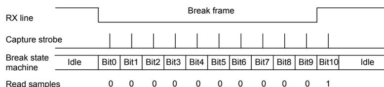
| RX line | Break frame | ||||||||||||
| Capture strobe | | | | | | | | | | | | | | | | | | | | | | | ||
| Break state machine | Idle | Bit0 | Bit1 | Bit2 | Bit3 | Bit4 | Bit5 | Bit6 | Bit7 | Bit8 | Bit9 | Bit10 | Idle |
| Read samples | 0 | 0 | 0 | 0 | 0 | 0 | 0 | 0 | 0 | 0 | 1 | ||
Case 2: break signal just long enough => break detected, LBDF is set
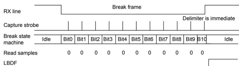
| RX line | Break frame | Delimiter is immediate | ||||||||||||
| Capture strobe | | | | | | | | | | | | | | | | | | | | | | | | | | | |
| Break state machine | Idle | Bit0 | Bit1 | Bit2 | Bit3 | Bit4 | Bit5 | Bit6 | Bit7 | Bit8 | Bit9 | Bit10 | Idle | |
| Read samples | 0 | 0 | 0 | 0 | 0 | 0 | 0 | 0 | 0 | 0 | 0 | |||
| LBDF | Set | |||||||||||||
Case 3: break signal long enough => break detected, LBDF is set
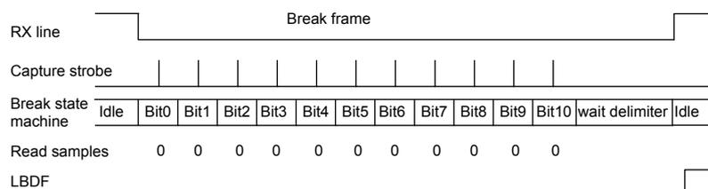
| RX line | Break frame | |||||||||||||
| Capture strobe | | | | | | | | | | | | | | | | | | | | | | | | | ||
| Break state machine | Idle | Bit0 | Bit1 | Bit2 | Bit3 | Bit4 | Bit5 | Bit6 | Bit7 | Bit8 | Bit9 | Bit10 | wait delimiter | Idle |
| Read samples | 0 | 0 | 0 | 0 | 0 | 0 | 0 | 0 | 0 | 0 | 0 | |||
| LBDF | Set | |||||||||||||
Case 1: break occurring after an Idle
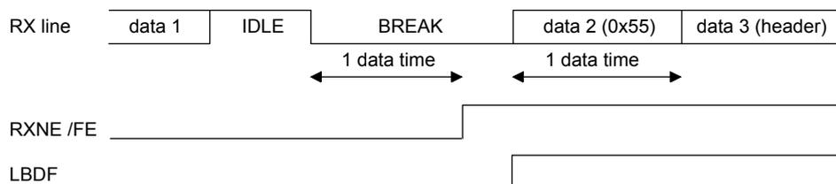
Timing diagram for Case 1: break occurring after an Idle. The RX line shows a sequence of data 1, IDLE, BREAK, data 2 (0x55), and data 3 (header). The BREAK duration is 1 data time. The RXNE/FE line is high during IDLE and low during BREAK. The LBDF line is high during IDLE and low during BREAK.
Case 2: break occurring while data is being received
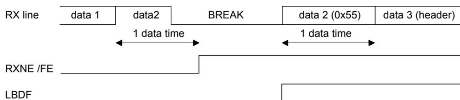
Timing diagram for Case 2: break occurring while data is being received. The RX line shows a sequence of data 1, data 2, BREAK, data 2 (0x55), and data 3 (header). The BREAK duration is 1 data time. The RXNE/FE line is high during data 1 and data 2, and low during BREAK. The LBDF line is high during data 1 and data 2, and low during BREAK.
22.5.12 USART synchronous mode
Master mode
The synchronous master mode is selected by writing the CLKEN bit in the USART_CR2 register to 1. In synchronous mode, the following bits must be kept cleared:
- • LINEN bit in the USART_CR2 register
- • SCEN, HDSEL and IREN bits in the USART_CR3 register.
In this mode, the USART can be used to control bidirectional synchronous serial communications in master mode. The SCLK pin is the output of the USART transmitter clock. No clock pulses are sent to the SCLK pin during start bit and stop bit. Depending on the state of the LBCL bit in the USART_CR2 register, clock pulses are, or are not, generated during the last valid data bit (address mark). The CPOL bit in the USART_CR2 register is used to select the clock polarity, and the CPHA bit in the USART_CR2 register is used to select the phase of the external clock (see Figure 136. USART example of synchronous master transmission and Figure 137. USART data clock timing diagram M=0).
During the idle state, preamble and send break, the external SCLK clock is not activated.
In synchronous master mode the USART transmitter works exactly like in asynchronous mode. But as SCLK is synchronized with TX (according to CPOL and CPHA), the data on TX is synchronous.
In this mode the USART receiver works in a different manner compared to the asynchronous mode. If RE=1, the data is sampled on SCLK (rising or falling edge, depending on CPOL and CPHA), without any oversampling. A setup and a hold time must be respected (which depends on the baud rate: 1/16 bit time).
Note: In master mode, the SCLK pin works in conjunction with the TX pin. Thus, the clock is provided only if the transmitter is enabled (TE=1) and data is being transmitted (the data register USART_DR written). This means that it is not possible to receive synchronous data without transmitting data.
Figure 136. USART example of synchronous master transmission
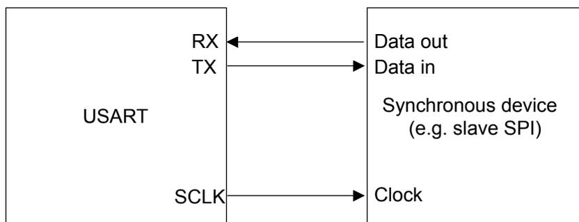
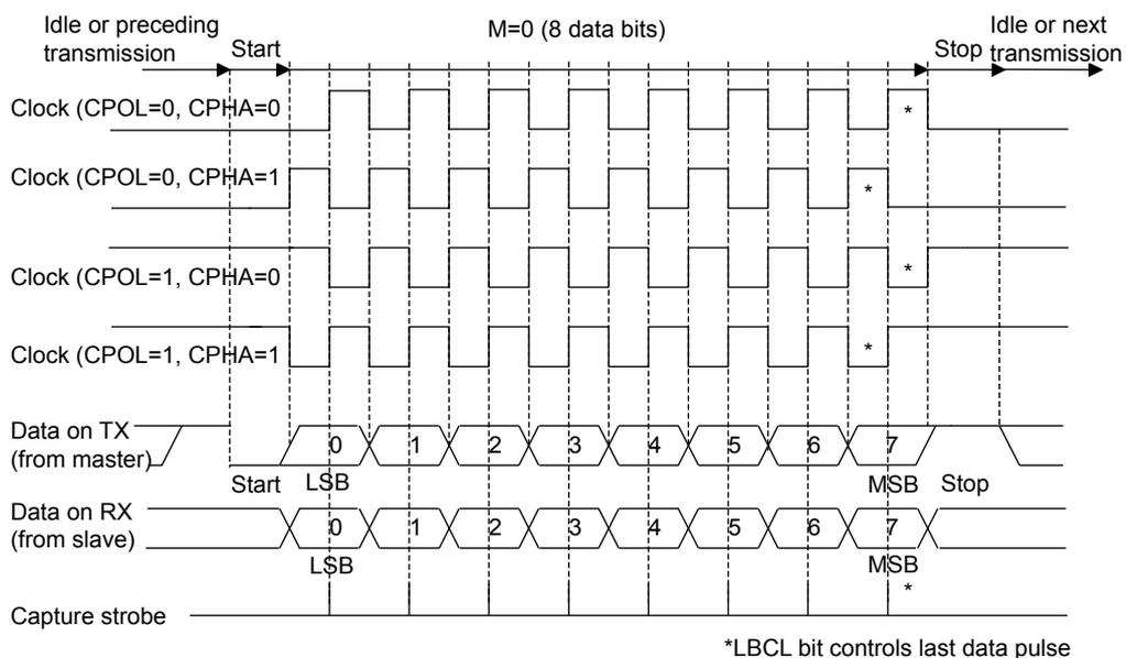
Figure 137. USART data clock timing diagram M=0
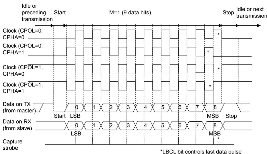
The diagram illustrates USART timing for 9 data bits (M=1). It shows four clock configurations based on CPOL (0 or 1) and CPHA (0 or 1). Below the clocks, 'Data on TX (from master)' and 'Data on RX (from slave)' waveforms show a Start bit, followed by data bits 0 through 8 (LSB to MSB), and a Stop bit. A 'Capture strobe' line indicates sampling points. Labels indicate 'Idle or preceding transmission', 'Start', 'M=1 (9 data bits)', 'Stop', and 'Idle or next transmission'. An asterisk note states: *LBCL bit controls last data pulse.
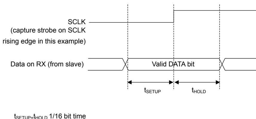
This diagram shows the timing relationship between the SCLK (capture strobe on rising edge) and the 'Data on RX (from slave)'. It defines \( t_{SETUP} \) as the time data must be valid before the rising edge and \( t_{HOLD} \) as the time it must remain valid after. Below the diagram, the relationship is defined as:
Slave mode
The synchronous slave mode is selected by writing the SLVEN bit in the USART_CR2 register to 1. In synchronous slave mode, the following bits must be kept cleared:
- • LINEN and CLKEN bits in the USART_CR2 register,
- • SCEN, HDSEL and IREN bits in the USART_CR3 register.
In this mode, the USART can be used to control bidirectional synchronous serial communications in slave mode. The SCLK pin is the input of the USART in slave mode.
Note: When the peripheral is used in SPI slave mode, the peripheral clock source (fck_pres) must be greater than 3xSCLK input clock.
The CPOL bit in the USART_CR2 register is used to select the clock polarity, and the CPHA bit in the USART_CR2 register is used to select the phase of the external clock (see Figure 136. USART example of synchronous master transmission , Figure 137. USART data clock timing diagram M=0 and Figure 138. USART data clock timing diagram (M bits = 01) ).
In slave transmission mode, an underun error flag is available. This flag is set when the first clock for data transmission appears while the software has not yet loaded any value into USARTx_TDR.
The slave supports the hardware and software NSS management.
Slave select (NSS) pin management
Hardware or software slave select management can be set using the DIS_NSS bit in the USART_CR2 register.
- • Software NSS management (DIS_NSS =1)
SPI slave is always selected and NSS input pin is ignored. The external NSS pin remains free for other application uses. - • Hardware NSS management (DIS_NSS =0)
The SPI slave selection depends on NSS input pin. The slave is selected when NSS is low and deselected when NSS high.
Note: The LBCL (used only on SPI master mode), CPOL and CPHA bits have to be selected when the USART is disabled (UE=0) to ensure that the clock pulses function correctly.
Note: When in SPI slave mode, the USART must be enabled before the master starts communication (or between frames while the clock is stable). Otherwise, if the USART slave is enabled while the master is in the middle of a frame, it becomes desynchronized with the master. The data register of the slave needs to be ready before the first edge of the communication clock or before the end of the on-going communication, otherwise SPI slave transmits zeros.
SPI slave underrun error
When an underrun error occurs, the SPI slave sends the last data until the underrun error flag is cleared in software.
The underrun flag is set at the beginning of the frame.
The underrun error flag is cleared by setting bit UDRCF in the USART_ICR register.
In underrun condition, it is allowed to write the TDR register. Clearing the underrun error would allow sending the new data.
If an underrun error occurred and there is no new data written in TDR, then the TC flag is set at the end of the frame.
Note: An underrun error may occur if the data is written in the USARTx_TDR too close to the first SCLK transmission edge. To avoid this underrun error, the USART_TDR should be written 3 UCLK cycles before the first SCLK edge.
22.5.13 Single-wire half-duplex communication
Single-wire half-duplex mode is selected by setting the HDSEL bit in the USART_CR3 register. In this mode, the following bits must be kept cleared:
- • LINEN and CLKEN bits in the USART_CR2 register
- • SCEN and IREN bits in the USART_CR3 register.
The USART can be configured to follow a single-wire half-duplex protocol where the TX and RX lines are internally connected. The selection between half- and full-duplex communication is made with a control bit HDSEL in USART_CR3.
As soon as HDSEL is written to 1:
- • The TX and RX lines are internally connected
- • The RX pin is no longer used
- • The TX pin is always released when no data is transmitted. Thus, it acts as a standard I/O in idle or in reception. It means that the I/O must be configured so that TX is configured as alternate function open-drain with an external pull-up.
Apart from this, the communication protocol is similar to normal USART mode. Any conflicts on the line must be managed by software (by the use of a centralized arbiter, for instance). In particular, the transmission is never blocked by hardware and continues as soon as data are written in the data register while the TE bit is set.
Note: As the TX line and the RX lines are connected together, all the transmitted data are stored in the RX FIFO as the data received from an external device. The software has to take care to discard its “own” information after a transmit phase. In half-duplex mode, it is always wise to read back the transmitted data to check if they are correct as there is no hardware protection against possible collision between nodes. If the software does not want to have the RX FIFO storing the transmitted value then it has to disable the receiver part while transmitting (by clearing the RE bit in USART_CR1 register).
22.5.14 Receiver timeout
The receiver timeout feature is enabled by setting the RTOEN bit in the USART_CR2 control register. The timeout duration is programmed using the RTO bit fields in the USARTx_RTOR register. The receiver timeout counter starts counting
- • From the end of the stop bit in case STOP = 00 and STOP = 11
- • From the end of the second stop bit in case STOP = 10
- • From the beginning of the stop bit in case STOP = 01.
When the timeout duration has elapsed, the RTOF flag in the USARTx_ISR register is set and a timeout is generated if RTOIE bit in USARTx_CR1 register is set.
22.5.15 Smartcard mode
This section is relevant only when smartcard mode is supported. Refer to Section 22.4: USART implementation . Smartcard mode is selected by setting the SCEN bit in the USART_CR3 register. In Smartcard mode, the following bits must be kept cleared:
- • LINEN bit in the USART_CR2 register
- • HDSEL and IREN bits in the USART_CR3 register.
The CLKEN bit may be set in order to provide a clock to the Smartcard.
The Smartcard interface is designed to support asynchronous protocol Smartcards as defined in the ISO 7816-3 standard. Both T=0 (character mode) and T=1 (block mode) are supported.
The USART should be configured as:
- • 8-bit plus parity: where M=1 and PCE=1 in the USART_CR1 register
- • 1.5 stop bits when transmitting and receiving data: where STOP=11 in the USART_CR2 register. It is also possible to choose the 0.5 stop bit for receiving.
In T=0 (character) mode, the parity error is indicated at the end of each character during the Guard Time period.
Figure 140. ISO 7816-3 asynchronous protocol shows examples of what can be seen on the data line with and without parity error.
Figure 140. ISO 7816-3 asynchronous protocol
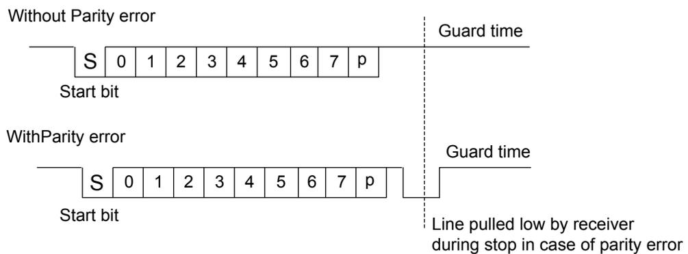
The diagram illustrates two timing scenarios for the ISO 7816-3 asynchronous protocol. Both show a sequence of bits: a Start bit (S), 8 data bits (0-7), and a parity bit (p). A vertical dashed line marks the 'Guard time' period. In the 'Without Parity error' scenario, the line returns to the idle state after the parity bit. In the 'With Parity error' scenario, the line is pulled low by the receiver during the stop bit period, which is indicated by the text 'Line pulled low by receiver during stop in case of parity error'.
When connected to a Smartcard, the TX output of the USART drives a bidirectional line that is also driven by the Smartcard. The TX pin must be configured as open drain.
Smartcard mode implements a single-wire half-duplex communication protocol.
- • Transmission of data from the transmit shift register is guaranteed to be delayed by a minimum of 1/2 baud clock. In a normal operation a full transmit shift register starts shifting on the next baud clock edge. In Smartcard mode this transmission is further delayed by a guaranteed 1/2 baud clock.
- • In transmission, if the Smartcard detects a parity error, it signals this condition to the USART by driving the line low (NACK). This NACK signal (pulling transmit line low for 1 baud clock) causes a framing error on the transmitter side (configured with 1.5 stop bits). The USART can handle automatic re-sending of data according to the protocol. The number of retries is programmed in the SCARCNT bit field. If the USART continues receiving the NACK after the programmed number of retries, it stops transmitting and signals the error as a framing error. The TXE bit (TXFNF bit in case FIFO mode is enabled) may be set using the TXFRQ bit in the USART_RQR register.
- • Smartcard auto-retry in transmission: a delay of 2.5 baud periods is inserted between the NACK detection by the USART and the start bit of the repeated character. The TC bit is set immediately at the end of reception of the last repeated character (no Guard Time). If the software wants to repeat it again, it must ensure the minimum 2 baud periods required by the standard.
- • If a parity error is detected during reception of a frame programmed with a 1.5 stop bit period, the transmit line is pulled low for a baud clock period after the completion of the receive frame. This is to indicate to the Smartcard that the data transmitted to the USART has not been correctly received. A parity error is NACKed by the receiver if the NACK control bit is set, otherwise a NACK is not transmitted (to be used in T=1 mode). If the received character is erroneous, the RXNE (RXFNE in case FIFO mode is enabled)/receive DMA request is not activated. According to the protocol specification, the Smartcard must resend the same character. If the received character is still erroneous after the maximum number of retries specified in the SCARCNT bit field, the USART stops transmitting the NACK and signals the error as a parity error.
- • Smartcard auto-retry in reception: the BUSY flag remains set if the USART NACKs the card but the card does not repeat the character.
- • In transmission, the USART inserts the Guard Time (as programmed in the Guard Time register) between two successive characters. As the Guard Time is measured after the stop bit of the previous character, the GT[7:0] register must be programmed to the desired CGT (Character Guard Time, as defined by the 7816-3 specification) minus 12 (the duration of one character).
- • The assertion of the TC flag can be delayed by programming the Guard Time register. In normal operation, TC is asserted when the transmit shift register is empty and no further transmit requests are outstanding. In Smartcard mode an empty transmit shift register triggers the Guard Time counter to count up to the programmed value in the Guard Time register. TC is forced low during this time. When the Guard Time counter reaches the programmed value TC is asserted high. The TCBGT flag can be used to detect the end of data transfer without waiting for Guard Time completion. This flag is set just after the end of frame transmission and if no NACK has been received from the card.
- • The deassertion of TC flag is unaffected by Smart card mode.
- • If a framing error is detected on the transmitter end (due to a NACK from the receiver), the NACK is not detected as a start bit by the receive block of the transmitter. According to the ISO protocol, the duration of the received NACK can be 1 or 2 baud clock periods.
- • On the receiver side, if a parity error is detected and a NACK is transmitted the receiver does not detect the NACK as a start bit.
Note: A break character is not significant in smartcard mode. A 0x00 data with a framing error is treated as data and not as a break.
Note: No Idle frame is transmitted when toggling the TE bit. The Idle frame (as defined for the other configurations) is not defined by the ISO protocol.
Figure 141. Parity error detection using 1.5 stop bits details how the NACK signal is sampled by the USART. In this example the USART is transmitting data and is configured with 1.5 stop bits. The receiver part of the USART is enabled in order to check the integrity of the data and the NACK signal.
Figure 141. Parity error detection using 1.5 stop bits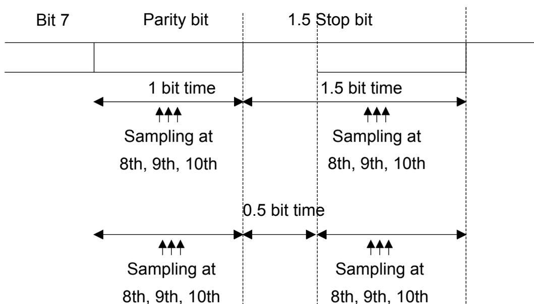
The diagram illustrates the sampling timing for parity and stop bits in a USART communication. It shows two horizontal timelines. The top timeline shows 'Bit 7' followed by a 'Parity bit' (duration: 1 bit time) and a '1.5 Stop bit' (duration: 1.5 bit time). Sampling for the parity bit occurs at the 8th, 9th, and 10th clock cycles within its 1-bit duration. Sampling for the stop bit also occurs at the 8th, 9th, and 10th clock cycles within its 1.5-bit duration. The bottom timeline shows a '0.5 bit time' interval followed by sampling at the 8th, 9th, and 10th clock cycles for a subsequent bit.
The USART can provide a clock to the Smartcard through the SCLK output. In Smartcard mode, SCLK is not associated to the communication but is simply derived from the internal peripheral input clock through a 5-bit prescaler. The division ratio is configured in the prescaler register USART_. SCLK frequency can be programmed from \( f_{CKPRES}/2 \) to \( f_{CKPRES}/62 \) , where \( f_{CKPRES} \) is the peripheral input clock divided by a programmed prescaler.
Block mode (T=1)
In T=1 (block) mode, the parity error transmission can be deactivated by clearing the NACK bit in the UART_CR3 register.
When requesting a read from the Smartcard, in block mode, the software must program the RTOR register to the BWT (block wait time) - 11 value. If no answer is received from the card before the expiration of this period, a timeout interrupt is generated. If the first character is received before the expiration of the period, it is signaled by the RXNE/RXFNE interrupt.
Note: The RXNE/RXFNE interrupt must be enabled even when using the USART in DMA mode to read from the Smartcard in block mode. In parallel, the DMA must be enabled only after the first received byte.
After the reception of the first character (RXNE/RXFNE interrupt), the RTO register must be programmed to the CWT (character wait time) - 11 value, in order to allow the automatic check of the maximum wait time between two consecutive characters. This time is expressed in baudtime units. If the Smartcard does not send a new character in less than the CWT period after the end of the previous character, the USART signals this to the software through the RTOF flag and interrupt (when RTOIE bit is set).
Note: As in the Smartcard protocol definition, the BWT/CWT values should be defined from the beginning (start bit) of the last character. The RTO register must be programmed to BWT - 11 or CWT - 11, respectively, taking into account the length of the last character itself.
A block length counter is used to count all the characters received by the USART. This counter is reset when the USART is transmitting. The length of the block is communicated by the Smartcard in the third byte of the block (prologue field). This value must be programmed to the BLEN field in the USART_RTOR register. When using DMA mode, before the start of the block, this register field must be programmed to the minimum value (0x0). With this value, an interrupt is generated after the 4th received character. The software must read the LEN field (third byte), its value must be read from the receive buffer.
In interrupt driven receive mode, the length of the block may be checked by software or by programming the BLEN value. However, before the start of the block, the maximum value of BLEN (0xFF) may be programmed. The real value is programmed after the reception of the third character.
If the block is using the LRC longitudinal redundancy check (1 epilogue byte), the BLEN=LEN. If the block is using the CRC mechanism (2 epilog bytes), BLEN=LEN+1 must be programmed. The total block length (including prologue, epilogue and information fields) equals BLEN+4. The end of the block is signaled to the software through the EOBF flag and interrupt (when EOBIE bit is set). In case of an error in the block length, the end of the block is signaled by the RTO interrupt (character wait time overflow).
Note: The error checking code (LRC/CRC) must be computed/verified by software.
Direct and inverse convention
The Smartcard protocol defines two conventions: direct and inverse.
The direct convention is defined as: LSB first, logical bit value of 1 corresponds to a H state of the line and parity is even. In order to use this convention, the following control bits must be programmed: MSBFIRST=0, DATAINV=0 (default values).
The inverse convention is defined as: MSB first, logical bit value 1 corresponds to an L state on the signal line and parity is even. In order to use this convention, the following control bits must be programmed: MSBFIRST=1, DATAINV=1.
Note: When logical data values are inverted (0=H, 1=L), the parity bit is also inverted in the same way.
In order to recognize the card convention, the card sends the initial character, TS, as the first character of the ATR (answer to reset) frame. The two possible patterns for the TS are: LHHL LLL LLH and LHHL HHH LLH.
- • (H) LHHL LLL LLH sets up the inverse convention: state L encodes value 1 and moment 2 conveys the most significant bit (MSB first). When decoded by inverse convention, the conveyed byte is equal to '3F'.
- • (H)LHHL HHH LLH sets up the direct convention: state H encodes value 1 and moment 2 conveys the least significant bit (LSB first). When decoded by direct convention, the conveyed byte is equal to '3B'.
Character parity is correct when there is an even number of bits set to 1 in the nine moments 2 to 10.
As the USART does not know which convention is used by the card, it needs to be able to recognize either pattern and act accordingly. The pattern recognition is not done in hardware, but through a software sequence. Moreover, supposing that the USART is configured in direct convention (default) and the card answers with the inverse convention, TS = LHHL LLL LLH => the USART received character is '03' and the parity is odd.
Therefore, two methods are available for TS pattern recognition:
Method 1
The USART is programmed in standard Smartcard mode/direct convention. In this case, the TS pattern reception generates a parity error interrupt and error signal to the card.
- • The parity error interrupt informs the software that the card did not answer correctly in direct convention. Software then reprograms the USART for inverse convention
- • In response to the error signal, the card retries the same TS character, and it is correctly received this time, by the reprogrammed USART.
Alternatively, in answer to the parity error interrupt, the software may decide to reprogram the USART and also to generate a new reset command to the card, then wait again for the TS.
Method 2
The USART is programmed in 9-bit/no-parity mode, no bit inversion. In this mode it receives either of the two TS patterns as:
- • (H) LHHL LLL LLH = 0x103 -> inverse convention to be chosen
- • (H) LHHL HHH LLH = 0x13B -> direct convention to be chosen.
The software checks the received character against these two patterns and, if either of them match, then programs the USART accordingly for the next character reception.
If neither of the two are recognized, a card reset may be generated in order to restart the negotiation.
22.5.16 IrDA SIR ENDEC block
This section is relevant only when IrDA mode is supported. Refer to Section 22.4: USART implementation .
IrDA mode is selected by setting the IREN bit in the USART_CR3 register. In IrDA mode, the following bits must be kept cleared:
- • LINEN, STOP and CLKEN bits in the USART_CR2 register
- • SCEN and HDSEL bits in the USART_CR3 register.
The IrDA SIR physical layer specifies use of a return to zero, inverted (RZI) modulation scheme that represents logic 0 as an infrared light pulse (see Figure 142. IrDA SIR ENDEC - block diagram ).
The SIR transmit encoder modulates the non-return-to-zero (NRZ) transmit bit stream output from USART. The output pulse stream is transmitted to an external output driver and infrared LED. USART supports only the bit rates up to 115.2 Kbps for the SIR ENDEC. In normal mode the transmitted pulse width is specified as 3/16 of a bit period.
The SIR receive decoder demodulates the return-to-zero bit stream from the infrared detector and outputs the received NRZ serial bit stream to the USART. The decoder input is normally high (marking state) in the idle state. The transmit encoder output has the opposite polarity to the decoder input. A start bit is detected when the decoder input is low.
- • IrDA is a half-duplex communication protocol. If the transmitter is busy (when the USART is sending data to the IrDA encoder), any data on the IrDA receive line is ignored by the IrDA decoder and if the receiver is busy (when the USART is receiving decoded data from the USART), data on the TX from the USART to IrDA is not encoded. While receiving data, transmission should be avoided as the data to be transmitted could be corrupted.
- • A 0 is transmitted as a high pulse and a 1 is transmitted as a 0. The width of the pulse is specified as 3/16th of the selected bit period in normal mode (see Figure 143. IrDA data modulation (3/16) - normal mode ).
- • The SIR decoder converts the IrDA compliant receive signal into a bit stream for USART.
- • The SIR receive logic interprets a high state as a logic one and low pulses as logic zeros.
- • The transmit encoder output has the opposite polarity to the decoder input. The SIR output is in low state when Idle.
- • The IrDA specification requires the acceptance of pulses greater than 1.41 µs. The acceptable pulse width is programmable. Glitch detection logic on the receiver end filters out pulses of width less than 2 PSC periods (PSC is the prescaler value programmed in the USART_GTPR). Pulses of width less than 1 PSC period are always rejected, but those of width greater than one and less than two periods may be accepted or rejected, those greater than 2 periods are accepted as a pulse. The IrDA encoder/decoder does not work when PSC=0.
- • The receiver can communicate with a low-power transmitter.
- • In IrDA mode, the STOP bits in the USART_CR2 register must be configured to “1 stop bit”.
IrDA low-power mode
Transmitter
In low-power mode the pulse width is not maintained at 3/16 of the bit period. Instead, the width of the pulse is 3 times the low-power baud rate which can be a minimum of 1.42 MHz. Generally, this value is 1.8432 MHz (1.42 MHz < PSC < 2.12 MHz). A low-power mode programmable divisor divides the system clock to achieve this value.
Receiver:
Receiving in low-power mode is similar to receiving in normal mode. For glitch detection the USART should discard pulses of duration shorter than 1/PSC. A valid low is accepted only if its duration is greater than 2 periods of the IrDA low-power baud clock (PSC value in the USART_GTPR).
Note: A pulse of width less than two and greater than one PSC period(s) may or may not be rejected.
Note: The receiver set-up time should be managed by software. The IrDA physical layer specification specifies a minimum of 10 ms delay between transmission and reception (IrDA is a half-duplex protocol).
Figure 142. IrDA SIR ENDEC - block diagram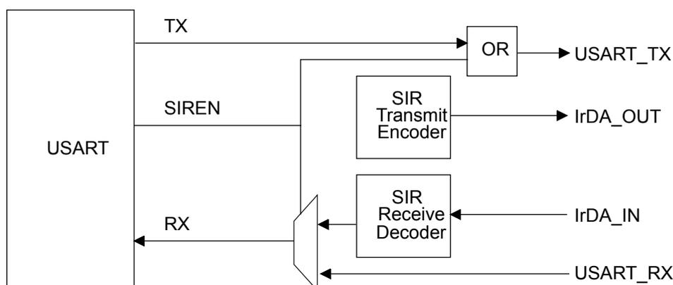
22.5.17 Continuous communication using DMA
The USART is capable of performing continuous communication using the DMA. The DMA requests for Rx buffer and Tx buffer are generated independently.
Note: Refer to Section 22.4: USART implementation to determine if the DMA mode is supported. If DMA is not supported, use the USART as explained in Section 22.5.4: Receiver . To perform continuous communication, when FIFO is disabled, you can clear the TXE/ RXNE flags in the USART_ISR register.
Transmission using DMA
DMA mode can be enabled for transmission by setting DMAT bit in the USART_CR3 register. Data are loaded from an SRAM area configured using the DMA peripheral (refer to Section 10: DMA controller (DMA) ) to the USART_TDR register whenever the TXE flag (TXFNF flag if FIFO mode is enabled) is set. To map a DMA channel for USART transmission, use the following procedure (x denotes the channel number):
- 1. Write the USART_TDR register address in the DMA control register to configure it as the destination of the transfer. The data are moved to this address from memory after each TXE (or TXFNF if FIFO mode is enabled) event.
- 2. Write the memory address in the DMA control register to configure it as the source of the transfer. The data is loaded into the USART_TDR register from this memory area after each TXE (or TXFNF if FIFO mode is enabled) event.
- 3. Configure the total number of bytes to be transferred to the DMA control register.
- 4. Configure the channel priority in the DMA register.
- 5. Configure DMA interrupt generation after half/ full transfer as required by the application.
- 6. Clear the TC flag in the USART_ISR register by setting the TCCF bit in the USART_ICR register.
- 7. Activate the channel in the DMA register.
When the number of data transfers programmed in the DMA controller is reached, the DMA controller generates an interrupt on the DMA channel interrupt vector.
In transmission mode, once the DMA has written all the data to be transmitted (the TCIF flag is set in the DMA_ISR register), the TC flag can be monitored to make sure that the USART communication is complete. This is required to avoid corrupting the last transmission before disabling the USART or entering Deepstop mode. Software must wait until TC=1. The TC flag remains cleared during all data transfers and it is set by hardware at the end of transmission of the last frame.
Figure 144. Transmission using DMA
| Software configures DMA to send 3 data blocks and enables USART | DMA writes F1 into USART_DR | DMA writes F2 into USART_DR | DMA writes F3 into USART_DR The DMA transfer is complete (TCIF=1 in DMA_ISR) | Software waits until TC=1 |
Note: When FIFO management is enabled, the DMA request is triggered by transmit FIFO not full (i.e. TXFNF = 1).
Reception using DMA
DMA mode can be enabled for reception by setting the DMAR bit in USART_CR3 register. Data is loaded from the USART_RDR register to an SRAM area configured using the DMA peripheral (refer to Section 10: DMA controller (DMA) ) whenever a data byte is received. To map a DMA channel for USART reception, use the following procedure:
- 1. Write the USART_RDR register address in the DMA control register to configure it as the source of the transfer. The data is moved from this address to the memory after each RXNE (RXFNE in case FIFO mode is enabled) event.
- 2. Write the memory address in the DMA control register to configure it as the destination of the transfer. The data is loaded from USART_RDR to this memory area after each RXNE (RXFNE in case FIFO mode is enabled) event.
- 3. Configure the total number of bytes to be transferred to the DMA control register.
- 4. Configure the channel priority in the DMA control register.
- 5. Configure interrupt generation after half/ full transfer as required by the application.
- 6. Activate the channel in the DMA control register.
When the number of data transfers programmed in the DMA controller is reached, the DMA controller generates an interrupt on the DMA channel interrupt vector.
Figure 145. Reception using DMA
Note: When FIFO management is enabled, the DMA request is triggered by ReceiveFIFO not empty (i.e. RXFNE = 1).
Error flagging and interrupt generation in multi-buffer communication
In multi-buffer communication if any error occurs during the transaction the error flag is asserted after the current byte. An interrupt is generated if the interrupt enable flag is set. For framing error, overrun error and noise flag which are asserted with RXNE ( RXFNE in case FIFO mode is enabled) in single byte reception, there is a separate error flag interrupt enable bit ( EIE bit in the USART_CR3 register), which, if set, enables an interrupt after the current byte if any of these errors occur.
22.5.18 RS232 hardware flow control and RS485 driver enable
It is possible to control the serial data flow between 2 devices by using the nCTS input and the nRTS output. Figure 146. Hardware flow control between 2 USARTs shows how to connect 2 devices in this mode.
Figure 146. Hardware flow control between 2 USARTs
RS232 RTS and CTS flow control can be enabled independently by writing the RTSE and CTSE bits respectively to 1 (in the USART_CR3 register).
RS232 RTS flow control
If the RTS flow control is enabled (RTSE=1), then nRTS is asserted (tied low) as long as the USART receiver is ready to receive new data. When the receive register is full, nRTS is deasserted, indicating that the transmission is expected to stop at the end of the current frame. Figure 147. RS232 RTS flow control shows an example of communication with RTS flow control enabled.
Figure 147. RS232 RTS flow control
Note: When FIFO mode is enabled, nRTS is deasserted only when RXFIFO is full.
RS232 CTS flow control
If the CTS flow control is enabled (CTSE=1), then the transmitter checks the nCTS input before transmitting the next frame. If nCTS is asserted (tied low), then the next data is transmitted (assuming that data is to be transmitted, in other words, if TXE/TXFE=0), otherwise the transmission does not occur. When nCTS is deasserted during a transmission, the current transmission is completed before the transmitter stops.
When CTSE=1, the CTSIF status bit is automatically set by hardware as soon as the CTS input toggles. It indicates when the receiver becomes ready or not ready for communication. An interrupt is generated if the CTSIE bit in the USART_CR3 register is set. Figure 148. RS232 CTS flow control shows an example of communication with CTS flow control enabled.
Figure 148. RS232 CTS flow control
Note: For correct behavior, nCTS must be asserted at least 3 USART clock source periods before the end of the current character. In addition it should be noted that the CTSCF flag may not be set for pulses shorter than 2 x PCLK periods.
RS485 driver enable
The driver enable feature is enabled by setting bit DEM in the USART_CR3 control register. This allows the user to activate the external transceiver control, through the DE (driver enable) signal. The assertion time is the time between the activation of the DE signal and the beginning of the START bit. It is programmed using the DEAT [4:0] bit fields in the USART_CR1 control register. The deassertion time is the time between the end of the last stop bit, in a transmitted message, and the de-activation of the DE signal. It is programmed using the DEDT [4:0] bit fields in the USART_CR1 control register. The polarity of the DE signal can be configured using the DEP bit in the USART_CR3 control register.
In USART, the DEAT and DEDT are expressed in sample time units (1/8 or 1/16 bit time, depending on the oversampling rate).
22.6 USART interrupts
Table 102. USART interrupt requests
| Interrupt event | Event flag | Enable control bit |
|---|---|---|
| Transmit data register empty | TXE | TXEIE |
| Transmit FIFO not full | TXFNF | TXFNFIE |
| Transmit FIFO empty | TXFE | TXFEIE |
| CTS interrupt | CTSIF | CTSIE |
| Transmission complete | TC | TCIE |
| Transmission complete before Guard Time | TCBGT | TCBGTIE |
| Receive data register not empty (data ready to be read) | RXNE | RXNEIE |
| Receive FIFO not empty | RXFNE | RXFNEIE |
| Receive FIFO full | RXFF | RXFFIE |
| Overrun error detected | ORE | RXNEIE/RXF- NEIE |
| Idle line detected | IDLE | IDLEIE |
| Parity error | PE | PEIE |
| LIN break | LBDF | LBDIE |
| Noise flag, overrun error and framing error in multi-buffer communication | NF or ORE or FE | EIE |
| Character match | CMF | CMIE |
| Receiver timeout error | RTOF | RTOIE |
| End of block | EOBF | EOBIE |
| SPI slave underrun error | UDR | EIE |
These events generate an interrupt if the corresponding enable control bit is set.
22.7 USART registers
Refer to Section 1.5: Acronyms for a list of abbreviations used in register descriptions.
22.7.1 Control register 1 (USARTx_CR1)
Address offset: 0x00
Reset value: 0x0000
| 31 | 30 | 29 | 28 | 27 | 26 | 25 | 24 | 23 | 22 | 21 | 20 | 19 | 18 | 17 | 16 |
|---|---|---|---|---|---|---|---|---|---|---|---|---|---|---|---|
| RXFFIE | TXFEIE | FIFOEN | M1 | EOBIE | RTOIE | DEAT[4:0] | DEDT[4:0] | ||||||||
| rw | rw | rw | rw | rw | rw | rw | rw | rw | rw | rw | rw | rw | rw | rw | rw |
| 15 | 14 | 13 | 12 | 11 | 10 | 9 | 8 | 7 | 6 | 5 | 4 | 3 | 2 | 1 | 0 |
| OVER8 | CMIE | MME | M0 | WAKE | PCE | PS | PEIE | TXEIE/ TXFNFIE | TCIE | RXNEIE /RXFNEIE | IDLEIE | TE | RE | Res. | UE |
| rw | rw | rw | rw | rw | rw | rw | rw | rw | rw | rw | rw | rw | rw | rw | |
| Bit 31 | RXFFIE : RXFIFO full interrupt enable. This bit is set and cleared by software. 0: Interrupt is inhibited 1: A USART interrupt is generated when RXFF=1 in the USART_ISR register Note: When FIFO mode is disabled, this bit is reserved and must be kept at reset value. |
| Bit 30 | TXFEIE : TXFIFO empty interrupt enable. This bit is set and cleared by software. 0: Interrupt is inhibited 1: A USART interrupt is generated when TXFE=1 in the USART_ISR register Note: When FIFO mode is disabled, this bit is reserved and must be kept at reset value. |
| Bit 29 | FIFOEN : FIFO mode enable. This bit is set and cleared by software. 0: FIFO mode is disabled 1: FIFO mode is enabled This bit field can only be written when the USART is disabled (UE=0). Note: FIFO mode can be used on standard UART communication, in SPI master/slave mode and in smartcard modes only. It must not be enabled in IrDA and LIN modes. |
| Bit 28 | M1 : Word length. This bit, with bit 12 (M0) determines the word length. It is set or cleared by software. M[1:0] = 00: 1 Start bit, 8 data bits, n Stop bit M[1:0] = 01: 1 Start bit, 9 data bits, n Stop bit M[1:0] = 10: 1 Start bit, 7 Data bits, n Stop bit This bit can only be written when the USART is disabled (UE=0). Note: In 7-bits data length mode, the smartcard mode, LIN master mode and auto baud rate (0x7F and 0x55 frames detection) are not supported. |
| Bit 27 | EOBIE : End of block interrupt enable. This bit is set and cleared by software. 0: Interrupt is inhibited 1: A USART interrupt is generated when the EOBF flag is set in the USART_ISR register Note: If the USART does not support Smartcard mode, this bit is reserved and forced by hardware to '0'. Refer to Section 22.4: USART implementation . |
| Bit 26 | RTOIE : Receiver timeout interrupt enable. This bit is set and cleared by software. 0: Interrupt is inhibited 1: A USART interrupt is generated when the RTOF bit is set in the USART_ISR register |
| Note: If the USART does not support the Receiver timeout feature, this bit is reserved and forced by hardware to '0'. Section 22.4: USART implementation. | |
| Bits 25:21 | DEAT[4:0]:
Driver enable assertion time. This 5-bit value defines the time between the activation of the DE (driver enable) signal and the beginning of the start bit. It is expressed in sample time units (1/8 or 1/16 bit time, depending on the oversampling rate). This bit field can only be written when the USART is disabled (UE=0). Note: If the driver enable feature is not supported, this bit is reserved and must be kept cleared. Refer to Section 22.4: USART implementation. |
| Bits 20:16 | DEDT[4:0]:
Driver enable deassertion time. This 5-bit value defines the time between the end of the last stop bit, in a transmitted message, and the deactivation of the DE (driver enable) signal. It is expressed in sample time units (1/8 or 1/16 bit time, depending on the oversampling rate). If the USART_TDR register is written during the DEDT time, the new data is transmitted only when the DEDT and DEAT times have both elapsed. This bit field can only be written when the USART is disabled (UE=0). Note: If the driver enable feature is not supported, this bit is reserved and must be kept cleared. Refer to Section 22.4: USART implementation. |
| Bit 15 | OVER8:
Oversampling mode. 0: Oversampling by 16 1: Oversampling by 8 This bit can only be written when the USART is disabled (UE=0). Note: In LIN, IrDA and Smartcard modes, this bit must be kept cleared. |
| Bit 14 | CMIE:
Character match interrupt enable. This bit is set and cleared by software. 0: Interrupt is inhibited 1: A USART interrupt is generated when the CMF bit is set in the USART_ISR register |
| Bit 13 | MME:
Mute mode enable. This bit activates the mute mode function of the USART. When set, the USART can switch between the active and mute modes, as defined by the WAKE bit. It is set and cleared by software. 0: Receiver in active mode permanently 1: Receiver can switch between mute mode and active mode |
| Bit 12 | M0:
Word length. This bit, with bit 28 (M1) determines the word length. It is set or cleared by software. See bit 28 (M1) description. This bit can only be written when the USART is disabled (UE=0). |
| Bit 11 | WAKE:
Receiver wakeup method. This bit determines the USART wakeup method from mute mode. It is set or cleared by software. 0: Idle line 1: Address mark This bit field can only be written when the USART is disabled (UE=0). |
| Bit 10 | PCE:
Parity control enable. This bit selects the hardware parity control (generation and detection). When the parity control is enabled, the computed parity is inserted at the MSB position (9 th bit if M=1; 8 th bit if M=0) and parity is checked on the received data. This bit is set and cleared by software. Once it is set, PCE is active after the current byte (in reception and in transmission). 0: Parity control disabled 1: Parity control enabled This bit field can only be written when the USART is disabled (UE=0). |
| Bit 9 | PS: Parity selection. |
This bit selects the odd or even parity when the parity generation/detection is enabled (PCE bit set). It is set and cleared by software. The parity is selected after the current byte. 0: Even parity This bit field can only be written when the USART is disabled (UE=0). | |
| Bit 8 | PEIE : PE interrupt enable. This bit is set and cleared by software. 0: Interrupt is inhibited |
| Bit 7 | TXEIE/TXFNFIE : Transmit data register empty/TXFIFO not full interrupt enable. This bit is set and cleared by software. 0: Interrupt is inhibited |
| Bit 6 | TCIE : Transmission complete interrupt enable. This bit is set and cleared by software. 0: Interrupt is inhibited |
| Bit 5 | RXNEIE/RXFNEIE : Receive data register not empty/RXFIFO not empty interrupt enable. This bit is set and cleared by software. 0: Interrupt is inhibited |
| Bit 4 | IDLEIE : IDLE interrupt enable. This bit is set and cleared by software. 0: Interrupt is inhibited |
| Bit 3 | TE : Transmitter enable. This bit enables the transmitter. It is set and cleared by software. 0: Transmitter is disabled Note: During transmission, a “0” pulse on the TE bit (“0” followed by “1”) sends a preamble (idleline) after the current word, except in Smartcard mode. In order to generate an idle character, the TE must not be immediately written to 1. In order to ensure the required duration, the software can poll the TEACK bit in the USART_ISR register. In Smartcard mode, when TE is set there is a 1 bit-time delay before the transmission starts. |
| Bit 2 | RE : Receiver enable. This bit enables the receiver. It is set and cleared by software. 0: Receiver is disabled |
| Bit 1 | Reserved, must be kept at reset value. |
| Bit 0 | UE : USART enable. When this bit is cleared, the USART prescalers and outputs are stopped immediately, and current operations are discarded. The configuration of the USART is kept, but all the status flags in the USART_ISR are reset. This bit is set and cleared by software. 0: USART prescaler and outputs disabled, low-power mode 1: USART enabled Note: In order to go into low-power mode without generating errors on the line, the TE bit must be reset before and the software must wait for the TC bit in the USART_ISR to be set before resetting the UE bit. The DMA requests are also reset when UE = 0 so the DMA channel must be disabled before resetting the UE bit. Note: In Smartcard mode, (SCEN = 1), the SCLK is always available when CLKEN = 1, regardless of the UE bit value. |
22.7.2 Control register 2 (USARTx_CR2)
Address offset: 0x04
Reset value: 0x0000
| 31 | 30 | 29 | 28 | 27 | 26 | 25 | 24 | 23 | 22 | 21 | 20 | 19 | 18 | 17 | 16 |
|---|---|---|---|---|---|---|---|---|---|---|---|---|---|---|---|
| ADD[7:4] | ADD[3:0] | RTOEN | ABRMOD[1:0] | ABREN | MSBFI | RST | DATAINV | TXINV | |||||||
| rw | rw | rw | rw | rw | rw | rw | rw | rw | rw | rw | rw | rw | rw | rw | rw |
| 15 | 14 | 13 | 12 | 11 | 10 | 9 | 8 | 7 | 6 | 5 | 4 | 3 | 2 | 1 | 0 |
| SWAP | LINEN | STOP[1:0] | CLKEN | CPOL | CPHA | LBCL | Res. | LBDIE | LBDL | ADD7 | DIS_N | SS. | Res. | SLVEN. | |
| rw | rw | rw | rw | rw | rw | rw | rw | rw | rw | rw | rw | rw | |||
| Bits 31:28 | ADD[7:4]: Address of the USART node. This bit-field gives the address of the USART node or a character code to be recognized. This is used in multiprocessor communication during Mute mode for wakeup with 7-bit address mark detection. The MSB of the character sent by the transmitter should be equal to 1. It may also be used for character detection during normal reception, Mute mode inactive (for example, end of block detection in ModBus protocol). In this case, the whole received character (8-bit) is compared to the ADD[7:0] value and CMF flag is set on match. This bit field can only be written when reception is disabled (RE=0) or the USART is disabled (UE=0). |
| Bits 27:24 | ADD[3:0]: Address of the USART node. This bit-field gives the address of the USART node or a character code to be recognized. This is used in multiprocessor communication during Mute mode, for wakeup with address mark detection. This bit field can only be written when reception is disabled (RE=0) or the USART is disabled (UE=0). |
| Bit 23 | RTOEN: Receiver timeout enable. This bit is set and cleared by software. 0: Receiver timeout feature disabled 1: Receiver timeout feature enabled When this feature is enabled, the RTOF flag in the USART_ISR register is set if the RX line is idle (no reception) for the duration programmed in the RTOR (receiver timeout register). Note: If the USART does not support the Receiver timeout feature, this bit is reserved and forced by hardware to '0'. Refer to Section 22.4: USART implementation . |
| Bit 22:21 | ABRMOD[1:0]: Auto baud rate mode. These bits are set and cleared by software. 00: Measurement of the start bit is used to detect the baud rate 01: Falling edge to falling edge measurement (the received frame must start with a single bit = 1 -> Frame = Start10xxxxxx) 10: 0x7F frame detection 11: 0x55 frame detection This bit field can only be written when ABREN=0 or the USART is disabled (UE=0). Note: If DATAINV=1 and/or MSBFIRST=1 the patterns must be the same on the line, for example 0xAA for MSBFIRST). If the USART does not support the auto baud rate feature, this bit is reserved and forced by hardware to '0'. Refer to Section 22.4: USART implementation . |
| Bit 20 | ABREN: Auto baud rate enable. This bit is set and cleared by software. 0: Auto baud rate detection is disabled 1: Auto baud rate detection is enabled Note: If the USART does not support the auto baud rate feature, this bit is reserved and forced by hardware to '0'. Refer to Section 22.4: USART implementation . |
| Bit 19 | MSBFIRST: Most significant bit first. This bit is set and cleared by software. 0: Data is transmitted/received with data bit 0 first, following the start bit |
| 1: Data is transmitted/received with the MSB (bit 7/8) first, following the start bit. This bit field can only be written when the USART is disabled (UE=0). | |
| Bit 18 | DATAINV:
Binary data inversion. This bit is set and cleared by software. 0: Logical data from the data register are sent/received in positive/direct logic. (1=H, 0=L) 1: Logical data from the data register are sent/received in negative/inverse logic. (1=L, 0=H). The parity bit is also inverted. This bit field can only be written when the USART is disabled (UE=0). |
| Bit 17 | TXINV:
TX pin active level inversion. This bit is set and cleared by software. 0: TX pin signal works using the standard logic levels (VDD=1/idle, Gnd=0/mark) 1: TX pin signal values are inverted. (VDD=0/mark, Gnd=1/idle). This allows the use of an external inverter on the TX line. This bit field can only be written when the USART is disabled (UE=0). |
| Bit 16 | RXINV:
RX pin active level inversion. This bit is set and cleared by software. 0: RX pin signal works using the standard logic levels (VDD=1/idle, Gnd=0/mark) 1: RX pin signal values are inverted. (VDD=0/mark, Gnd=1/idle). This allows the use of an external inverter on the RX line. This bit field can only be written when the USART is disabled (UE=0). |
| Bit 15 | SWAP:
Swap TX/RX pins. This bit is set and cleared by software. 0: TX/RX pins are used as defined in standard pinout 1: The TX and RX pins functions are swapped. This helps to work in the case of a cross-wired connection to another UART. This bit field can only be written when the USART is disabled (UE=0). |
| Bit 14 | LINEN:
LIN mode enable. This bit is set and cleared by software. 0: LIN mode disabled 1: LIN mode enabled The LIN mode enables the capability to send LIN Synch Breaks (13 low bits) using the SBKRQ bit in the USART_CR1 register, and to detect LIN Sync breaks. This bit field can only be written when the USART is disabled (UE=0). Note: If the USART does not support LIN mode, this bit is reserved and forced by hardware to '0'. Refer to Section 22.4: USART implementation . |
| Bits 13:12 | STOP[1:0]:
STOP bits. These bits are used for programming the stop bits. 00: 1 stop bit 01: 0.5 stop bit 10: 2 stop bits 11: 1.5 stop bits This bit field can only be written when the USART is disabled (UE=0). |
| Bit 11 | CLKEN:
Clock enable. This bit allows the user to enable the SCLK pin. 0: SCLK pin disabled 1: SCLK pin enabled This bit can only be written when the USART is disabled (UE=0). Note: If neither synchronous mode nor Smartcard mode is supported, this bit is reserved and forced by hardware to '0'. Refer to Section 22.4: USART implementation . Note: In Smartcard mode, in order to provide correctly the SCLK clock to the smartcard, the steps below must be respected: |
| |
| Bit 10 | CPOL: Clock polarity. This bit allows the user to select the polarity of the clock output on the SCLK pin in synchronous mode. It works in conjunction with the CPHA bit to produce the desired clock/data relationship. 0: Steady low value on SCLK pin outside transmission window 1: Steady high value on SCLK pin outside transmission window This bit can only be written when the USART is disabled (UE=0). Note: If synchronous mode is not supported, this bit is reserved and forced by hardware to '0'. Refer to Section 22.4: USART implementation . |
| Bit 9 | CPHA: Clock phase. This bit is used to select the phase of the clock output on the SCLK pin in synchronous mode. It works in conjunction with the CPOL bit to produce the desired clock/data relationship (see Figure 137. USART data clock timing diagram M=0 and Figure 138. USART data clock timing diagram (M bits = 01) ). 0: The first clock transition is the first data capture edge 1: The second clock transition is the first data capture edge This bit can only be written when the USART is disabled (UE=0). Note: If synchronous mode is not supported, this bit is reserved and forced by hardware to '0'. Refer to Section 22.4: USART implementation . |
| Bit 8 | LBCL: Last bit clock pulse. This bit is used to select whether the clock pulse associated with the last data bit transmitted (MSB) has to be output on the SCLK pin in synchronous mode. 0: The clock pulse of the last data bit is not output to the SCLK pin 1: The clock pulse of the last data bit is output to the SCLK pin Caution: The last bit is the 7 th or 8 th or 9 th data bit transmitted depending on the 7 or 8 or 9 bit format selected by the M bit in the USART_CR1 register. This bit can only be written when the USART is disabled (UE=0). Note: If synchronous mode is not supported, this bit is reserved and forced by hardware to '0'. Refer to Section 22.4: USART implementation . |
| Bit 7 | Reserved, must be kept at reset value. |
| Bit 6 | LBDIE: LIN break detection interrupt enable. Break interrupt mask (break detection using break delimiter). 0: Interrupt is inhibited 1: An interrupt is generated whenever LBDIF=1 in the USART_ISR register Note: If LIN mode is not supported, this bit is reserved and forced by hardware to '0'. Refer to Section 22.4: USART implementation . |
| Bit 5 | LBDL: LIN break detection length. This bit is for selection between 11 bit or 10 bit break detection. 0: 10-bit break detection 1: 11-bit break detection This bit can only be written when the USART is disabled (UE=0). Note: If LIN mode is not supported, this bit is reserved and forced by hardware to '0'. Refer to Section 22.4: USART implementation . |
| Bit 4 | ADD7: 7-bit address detection/4-bit address detection. This bit is for selection between 4-bit address detection or 7-bit address detection. 0: 4-bit address detection. 1: 7-bit address detection (in 8-bit data mode) |
| This bit can only be written when the USART is disabled (UE=0). Note: In 7-bit and 9-bit data modes, the address detection is done on 6-bit and 8-bit address (ADD[5:0] and ADD[7:0]) respectively. | |
| Bit 3 | DIS_NSS When the DIS_NSS bit is set, the NSS pin input is ignored. 0: SPI slave selection depends on NSS input pin 1: SPI slave is always selected and NSS input pin is ignored Note: When SPI slave mode is not supported, this bit is reserved and must be kept at reset value. |
| Bit 2 | Reserved, must be kept at reset value. |
| Bit 1 | Reserved, must be kept at reset value. |
| Bit 0 | SLVEN
: Synchronous slave mode enable. When the SLVEN bit is set, the synchronous slave mode is enabled. 0: Slave mode disabled 1: Slave mode enabled Note: When SPI slave mode is not supported, this bit is reserved and must be kept at reset value. |
Note: The CPOL, CPHA and LBCL bits should not be written while the transmitter is enabled.
22.7.3 Control register 3 (USARTx_CR3)
Address offset: 0x08
Reset value: 0x0000
| 31 | 30 | 29 | 28 | 27 | 26 | 25 | 24 | 23 | 22 | 21 | 20 | 19 | 18 | 17 | 16 |
|---|---|---|---|---|---|---|---|---|---|---|---|---|---|---|---|
| TXFTCFG | RXFTI E. | RXFTCFG | TCBGT IE | TXFTIE | Res. | Res. | SCARCNT2:0] | Res. | |||||||
| rw | rw | rw | rw | rw | rw | rw | rw | ||||||||
| 15 | 14 | 13 | 12 | 11 | 10 | 9 | 8 | 7 | 6 | 5 | 4 | 3 | 2 | 1 | 0 |
| DEP | DEM | DDRE | OVR DIS | ONE BIT | CTSIE | CTSE | RTSE | DMAT | DMAR | SCEN | NACK | HD SEL | IRLP | IREN | EIE |
| rw | rw | rw | rw | rw | rw | rw | rw | rw | rw | rw | rw | rw | rw | rw | rw |
| Bits 31:29 | TXFTCFG:
TXFIFO threshold configuration. 000: TXFIFO reaches 1/8 of its depth 001: TXFIFO reaches 1/4 of its depth 010: TXFIFO reaches 1/2 of its depth 011: TXFIFO reaches 3/4 of its depth. 100:TXFIFO reaches 7/8 of its depth. 101: TXFIFO becomes empty Remaining combinations: Reserved. |
| Bit28 | RXFTIE:
RXFIFO threshold interrupt enable. This bit is set and cleared by software. 0: Interrupt is inhibited 1: A USART interrupt is generated when Receive FIFO reaches the threshold programmed in RXFTCFG |
| Bits 27:25 | RXFTCFG:
Receive FIFO threshold configuration. 000: Receive FIFO reaches 1/8 of its depth 001: Receive FIFO reaches 1/4 of its depth 010: Receive FIFO reaches 1/2 of its depth 011: Receive FIFO reaches 3/4 of its depth 100: Receive FIFO reaches 7/8 of its depth 101: Receive FIFO becomes full Remaining combinations: Reserved. |
| Bit 24 | TCBGTIE:
Transmission complete before Guard Time, interrupt enable. This bit is set and cleared by software. 0: Interrupt is inhibited 1: A USART interrupt is generated whenever TCBGT=1 in the USARTx_ISR register Note: If the USART does not support the Smartcard mode, this bit is reserved and forced by hardware to '0'. |
| Bit 23 | TXFTIE:
TXFIFO threshold interrupt enable. This bit is set and cleared by software. 0: Interrupt is inhibited 1: A USART interrupt is generated when TXFIFO reaches the threshold programmed in TXFTCFG |
| Bits 22:20 | Reserved, must be kept at reset value. |
| Bit 19:17 | SCARCNT[2:0]:
Smartcard auto-retry count. This bit-field specifies the number of retries in transmit and receive, in Smartcard mode. In transmission mode, it specifies the number of automatic retransmission retries, before generating a transmission error (FE bit set). In reception mode, it specifies the number or erroneous reception trials, before generating a reception error (RXNE/RXFNE and PE bits set). This bit field must be programmed only when the USART is disabled (UE=0). |
When the USART is enabled (UE=1), this bit field may only be written to 0x0, in order to stop retransmission. 0x0: Retransmission disabled - No automatic retransmission in transmit mode 0x1 to 0x7: Number of automatic retransmission attempts (before signaling error) Note: If Smartcard mode is not supported, this bit is reserved and forced by hardware to '0'. Refer to Section 22.4: USART implementation . | |
| Bit 16 | Reserved, must be kept at reset value. |
| Bit 15 | DEP: Driver enable polarity selection. 0: DE signal is active high 1: DE signal is active low This bit can only be written when the USART is disabled (UE=0). Note: If the driver enable feature is not supported, this bit is reserved and must be kept cleared. Refer to Section 22.4: USART implementation . |
| Bit 14 | DEM: Driver enable mode. This bit allows the user to activate the external transceiver control, through the DE signal. 0: DE function is disabled 1: DE function is enabled. The DE signal is output on the RTS pin. This bit can only be written when the USART is disabled (UE=0). Note: If the driver enable feature is not supported, this bit is reserved and must be kept cleared. Section 22.4: USART implementation . |
| Bit 13 | DDRE: DMA disable on reception error. 0: DMA is not disabled in case of reception error. The corresponding error flag is set but RXNE is kept 0 preventing from overrun. As a consequence, the DMA request is not asserted, so the erroneous data is not transferred (no DMA request), but next correct received data are transferred (used for Smartcard mode). 1: DMA is disabled following a reception error. The corresponding error flag is set, as well as RXNE. The DMA request is masked until the error flag is cleared. This means that the software must first disable the DMA request (DMAR=0) or clear RXNE (RXFNE in case FIFO mode is enabled) before clearing the error flag. This bit can only be written when the USART is disabled (UE=0). Note: The reception errors are: parity error, framing error or noise error. |
| Bit 12 | OVRDIS: Overrun disable. This bit is used to disable the receive overrun detection. 0: Overrun error flag, ORE, is set when received data is not read before receiving new data 1: Overrun functionality is disabled. If new data is received while the RXNE flag is still set the ORE flag is not set and the new received data overwrites the previous content of the USART_RDR register. When FIFO mode is enabled, the RXFIFO is bypassed and data are written directly in USARTx_RDR register. Even when FIFO management is enabled, the RXNE flag is to be used. This bit can only be written when the USART is disabled (UE=0). Note: This control bit allows checking the communication flow w/o reading the data. |
| Bit 11 | ONEBIT: One sample bit method enable. This bit allows the user to select the sample method. When the one sample bit method is selected the noise detection flag (NF) is disabled. 0: Three sample bit method 1: One sample bit method This bit can only be written when the USART is disabled (UE=0). |
| Bit 10 | CTSIE: CTS interrupt enable. 0: Interrupt is inhibited 1: An interrupt is generated whenever CTSIF=1 in the USART_ISR register Note: If the hardware flow control feature is not supported, this bit is reserved and forced by hardware to '0'. Refer to Section 22.4: USART implementation . |
| Bit 9 | CTSE: CTS enable. |
0: CTS hardware flow control disabled 1: CTS mode enabled, data are only transmitted when the nCTS input is asserted (tied to 0). If the nCTS input is deasserted while data is being transmitted, then the transmission is completed before stopping. If data are written into the data register while nCTS is asserted, the transmission is postponed until nCTS is asserted. This bit can only be written when the USART is disabled (UE=0). Note: If the hardware flow control feature is not supported, this bit is reserved and forced by hardware to '0'. Refer to Section 22.4: USART implementation . | |
| Bit 8 | RTSE : RTS enable. 0: RTS hardware flow control disabled 1: RTS output enabled, data are only requested when there is space in the receive buffer. The transmission of data is expected to cease after the current character has been transmitted. The nRTS output is asserted (pulled to 0) when data can be received. This bit can only be written when the USART is disabled (UE=0). Note: If the hardware flow control feature is not supported, this bit is reserved and forced by hardware to '0'. Refer to Section 22.4: USART implementation . |
| Bit 7 | DMAT : DMA enable transmitter. This bit is set/reset by software. 1: DMA mode is enabled for transmission 0: DMA mode is disabled for transmission |
| Bit 6 | DMAR : DMA enable receiver. This bit is set/reset by software. 1: DMA mode is enabled for reception 0: DMA mode is disabled for reception |
| Bit 5 | SCEN : Smartcard mode enable. This bit is used for enabling Smartcard mode. 0: Smartcard mode disabled 1: Smartcard mode enabled This bit field can only be written when the USART is disabled (UE=0). Note: If the USART does not support Smartcard mode, this bit is reserved and forced by hardware to '0'. Refer to Section 22.4: USART implementation . |
| Bit 4 | NACK : Smartcard NACK enable. 0: NACK transmission in case of parity error is disabled 1: NACK transmission during parity error is enabled This bit field can only be written when the USART is disabled (UE=0). Note: If the USART does not support Smartcard mode, this bit is reserved and forced by hardware to '0'. Refer to Section 22.4: USART implementation . |
| Bit 3 | HDSEL : Half-duplex selection. Selection of single-wire half-duplex mode. 0: Half-duplex mode is not selected 1: Half-duplex mode is selected This bit can only be written when the USART is disabled (UE=0). |
| Bit 2 | IRLP : IrDA low-power. This bit is used for selecting between normal and low-power IrDA modes. 0: Normal mode 1: Low-power mode This bit can only be written when the USART is disabled (UE=0). Note: If IrDA mode is not supported, this bit is reserved and forced by hardware to '0'. Refer to Section 22.4: USART implementation |
| Bit 1 | IREN : IrDA mode enable. This bit is set and cleared by software. |
0: IrDA disabled 1: IrDA enabled This bit can only be written when the USART is disabled (UE=0). Note: If IrDA mode is not supported, this bit is reserved and forced by hardware to '0'. Refer to Section 22.4: USART implementation . | |
| Bit 0 | EIE: Error interrupt enable. Error interrupt enable bit is required to enable interrupt generation in case of a framing error, overrun error noise flag or SPI slave underrun error (FE=1 or ORE=1 or NF=1 or UDR = 1 in the USART_ISR register). 0: Interrupt is inhibited 1: An interrupt is generated when FE=1 or ORE=1 or NF=1 or UDR = 1 (in SPI slave mode) in the USART_ISR register |
22.7.4 Baud rate register (USARTx_BRR)
This register can only be written when the USART is disabled (UE=0). It may be automatically updated by hardware in auto baud rate detection mode.
Address offset: 0x0C
Reset value: 0x0000
| 31 | 30 | 29 | 28 | 27 | 26 | 25 | 24 | 23 | 22 | 21 | 20 | 19 | 18 | 17 | 16 |
| Res. | Res. | Res. | Res. | Res. | Res. | Res. | Res. | Res. | Res. | Res. | Res. | Res. | Res. | Res. | Res. |
| 15 | 14 | 13 | 12 | 11 | 10 | 9 | 8 | 7 | 6 | 5 | 4 | 3 | 2 | 1 | 0 |
| BRR[15:0] | |||||||||||||||
| rw | rw | rw | rw | rw | rw | rw | rw | rw | rw | rw | rw | rw | rw | rw | rw |
| Bits 31:16 | Reserved, must be kept at reset value. |
| Bits 15:4 | BRR[15:4] BRR[15:4] = USARTDIV[15:4] |
| Bits 3:0 | BRR[3:0] When OVER8 = 0, BRR[3:0] = USARTDIV[3:0]. When OVER8 = 1: BRR[2:0] = USARTDIV[3:0] shifted 1 bit to the right. BRR[3] must be kept cleared. |
22.7.5 Guard Time and prescaler register (USARTx_GTPR)
Address offset: 0x10
Reset value: 0x0000
| 31 | 30 | 29 | 28 | 27 | 26 | 25 | 24 | 23 | 22 | 21 | 20 | 19 | 18 | 17 | 16 |
| Res. | Res. | Res. | Res. | Res. | Res. | Res. | Res. | Res. | Res. | Res. | Res. | Res. | Res. | Res. | Res. |
| 15 | 14 | 13 | 12 | 11 | 10 | 9 | 8 | 7 | 6 | 5 | 4 | 3 | 2 | 1 | 0 |
| GT[7:0] | PSC[7:0] | ||||||||||||||
| rw | rw | ||||||||||||||
| Bits 31:16 | Reserved, must be kept at reset value. |
| Bits 15:8 | GT[7:0]: Guard Time value. This bit-field is used to program the Guard Time value in terms of number of baud clock periods. This is used in smartcard mode. The transmission complete flag is set after this Guard Time value. This bit field can only be written when the USART is disabled (UE=0). Note: If smartcard mode is not supported, this bit is reserved and forced by hardware to '0'. Refer to Section 22.4: USART implementation . |
| Bits 7:0 | PSC[7:0]: Prescaler value. In IrDA Low-power and normal IrDA mode: |
22.7.6 Receiver timeout register (USARTx_RTOR)
Address offset: 0x14
Reset value: 0x0000
| BLEN[7:0] | RTO[23:16] | ||||||||||||||
|---|---|---|---|---|---|---|---|---|---|---|---|---|---|---|---|
| rw | rw | rw | rw | rw | rw | rw | rw | rw | rw | rw | rw | rw | rw | rw | rw |
| 15 | 14 | 13 | 12 | 11 | 10 | 9 | 8 | 7 | 6 | 5 | 4 | 3 | 2 | 1 | 0 |
| RTO[15:0] | |||||||||||||||
| rw | rw | rw | rw | rw | rw | rw | rw | rw | rw | rw | rw | rw | rw | rw | rw |
| 15 | 14 | 13 | 12 | 11 | 10 | 9 | 8 | 7 | 6 | 5 | 4 | 3 | 2 | 1 | 0 |
| Bits 31:24 | BLEN[7:0]: Block length. This bit-field gives the block length in Smartcard T=1 Reception. Its value equals the number of information characters + the length of the epilogue field (1-LEC/2-CRC) - 1. Examples: In Smartcard mode, the Block length counter is reset when TXE=0 (TXFE=0 in case FIFO mode is enabled). This bit-field can be used also in other modes. In this case, the Block length counter is reset when RE=0 (receiver disabled) and/or when the EOBCF bit is written to 1. Note: This value can be programmed after the start of the block reception (using the data from the LEN character in the prologue field). It must be programmed only once per received block. |
| Bits 23:0 | RTO[23:0]: Receiver timeout value. This bit-field gives the Receiver timeout value in terms of number of baud clocks. In standard mode, the RTOF flag is set if, after the last received character, no new start bit is detected for more than the RTO value. In Smartcard mode, this value is used to implement the CWT and BWT. See Smartcard section for more details. In the standard, the CWT/BWT measurement is done starting from the start bit of the last received character. Note: This value must only be programmed once per received character. |
Note: RTOR can be written on the fly. If the new value is lower than or equal to the counter, the RTOF flag is set. This register is reserved and forced by hardware to “0x00000000” when the receiver timeout feature is not supported. Refer to Section 22.4: USART implementation.
22.7.7 Request register (USARTx_RQR)
Address offset: 0x18
Reset value: 0x0000
| 31 | 30 | 29 | 28 | 27 | 26 | 25 | 24 | 23 | 22 | 21 | 20 | 19 | 18 | 17 | 16 |
|---|---|---|---|---|---|---|---|---|---|---|---|---|---|---|---|
| Res. | Res. | Res. | Res. | Res. | Res. | Res. | Res. | Res. | Res. | Res. | Res. | Res. | Res. | Res. | Res. |
| 15 | 14 | 13 | 12 | 11 | 10 | 9 | 8 | 7 | 6 | 5 | 4 | 3 | 2 | 1 | |
| Res. | Res. | Res. | Res. | Res. | Res. | Res. | Res. | Res. | Res. | Res. | TXFRQ | RXFRQ | MMRQ | SBKRQ | ABRRQ |
| w_r0 | w_r0 | w_r0 | w_r0 | w_r0 |
| Bits 31:5 | Reserved, must be kept at reset value. |
| Bit 4 | TXFRQ: Transmit data flush request. When FIFO mode is disabled, writing 1 to this bit sets the TXE flag. This allows the transmit data to be discarded. This bit must be used only in Smartcard mode, when data has not been sent due to errors (NACK) and the FE flag is active in the USART_ISR register. If the USART does not support Smartcard mode, this bit is reserved and forced by hardware to '0'. When FIFO is enabled, TXFRQ bit is set to flush the whole FIFO. This sets the flag TXFE (transmit FIFO empty, bit 23 in the USART_ISR register). Flushing the transmit FIFO is supported in both UART and Smartcard modes. Note: In FIFO mode, the TXFNF flag is reset during the flush request until TXFIFO is empty in order to ensure that no data is written in the data register. |
| Bit 3 | RXFRQ: Receive data flush request. Writing 1 to this bit empties the entire receive FIFO, i.e. clears the bit RXFNE. This allows the received data to be discarded without reading them, and avoid an overrun condition. |
| Bit 2 | MMRQ: Mute mode request. Writing 1 to this bit puts the USART in mute mode and resets the RWU flag. |
| Bit 1 | SBKRQ: Send break request. Writing 1 to this bit sets the SBKF flag and requests to send a BREAK on the line, as soon as the transmit machine is available. Note: In the case the application needs to send the break character following all previously inserted data, including the ones not yet transmitted, the software should wait for the TXE flag assertion before setting the SBKRQ bit. |
| Bit 0 | ABRRQ: Auto baud rate request. Writing 1 to this bit resets the ABRF flag in the USART_ISR and requests an automatic baud rate measurement on the next received data frame. Note: If the USART does not support the auto baud rate feature, this bit is reserved and forced by hardware to '0'. Refer to Section 22.4: USART implementation . |
22.7.8 Interrupt and status register (USARTx_ISR)
Address offset: 0x1C
Reset value: 0x00C0 (in case FIFO disabled).
Reset value: 0x28000C0 (in case FIFO/Smartcard mode enabled).
Reset value: 0x08000C0 (in case FIFO enabled/Smartcard mode disabled).
| 31 | 30 | 29 | 28 | 27 | 26 | 25 | 24 | 23 | 22 | 21 | 20 | 19 | 18 | 17 | 16 |
|---|---|---|---|---|---|---|---|---|---|---|---|---|---|---|---|
| Res. | Res. | Res. | Res. | TXFT | RXFT | TCBGT | RXFF | TXFE | RE ACK | TE ACK | Res. | RWU | SBKF | CMF | BUSY |
| r | r | r | r | r | r | r | r | r | r | r | |||||
| 15 | 14 | 13 | 12 | 11 | 10 | 9 | 8 | 7 | 6 | 5 | 4 | 3 | 2 | 1 | 0 |
| ABRF | ABRE | UDR | EOBF | RTOF | CTS | CTSIF | LBDF | TXE/TX FNF | TC | RXNE/ RXFNE | IDLE | ORE | NF | FE | PE |
| r | r | r | r | r | r | r | r | r | r | r | r | r | r | r | r |
| Bits 31:28 | Reserved, must be kept at reset value. |
| Bit 27 | TXFT: TXFIFO threshold flag. This bit is set by hardware when the TXFIFO reaches the programmed threshold in TXFTCFG in USARTx_CR3 register i.e. the TXFIFO contains TXFTCFG empty locations. An interrupt is generated if the TXFTIE bit = 1 (bit 31) in the USART_CR3 register. 0: TXFIFO doesn't reach the programmed threshold |
| Bit 26 | RXFT: RXFIFO threshold flag. This bit is set by hardware when the programmed threshold in RXFTCFG in USARTx_CR3 register is reached. This means that there are (RXFTCFG - 1) data in the Receive FIFO and one data in the USART_RDR register. An interrupt is generated if the RXFTIE bit = 1 (bit 27) in the USART_CR3 register. 0: Receive FIFO does not reach the programmed threshold Note: When the RXFTCFG threshold is configured to «101», RXFT flag is set if 16 data are available, i.e. 15 data in the RXFIFO and 1 data in the USARTx_RDR. Consequently, the 17 th received data do not cause an overrun error. The overrun error occurs after receiving the 18 th data. |
| Bit 25 | TCBGT: Transmission complete before Guard Time flag. This bit indicates when the last data written in the USART_TDR has been transmitted correctly out of the shift register. It is set by hardware in Smartcard mode, if the transmission of a frame containing data is complete and if there is no NACK from the smartcard. An interrupt is generated if TCBGTIE=1 in the USART_CR3 register. It is cleared by software, writing 1 to the TCBGTIF in the USART_ICR register or by a write to the USART_TDR register. 0: Transmission is not complete or transmission is complete unsuccessfully (i.e. a NACK is received from the card) Note: If the USART does not support the Smartcard mode, this bit is reserved and forced by hardware to '0'. If the USART supports the Smartcard mode and the Smartcard mode is enabled, the TCBGT reset value is "1". |
| Bit 24 | RXFF: RXFIFO full. This bit is set by hardware when RXFIFO is full. An interrupt is generated if the RXFFIE bit = 1 in the USART_CR1 register. 0: RXFIFO is not full |
| Bit 23 | TXFE: TXFIFO empty. This bit is set by hardware when TXFIFO is Empty. When the TXFIFO contains at least one data, this flag is cleared. The TXFE flag can also be set by writing 1 to the bit TXFRQ (bit 4) in the USART_RQR register. An interrupt is generated if the TXFEIE bit = 1 (bit 30) in the USART_CR1 register. |
| 0: TXFIFO is not empty 1: TXFIFO is empty | |
| Bit 22 | REACK:
Receive enable acknowledge flag. This bit is set/reset by hardware, when the receive enable value is taken into account by the USART. It can be used to verify that the USART is ready for reception before entering Deepstop mode. Note: If the USART does not support the wakeup from Deepstop feature, this bit is reserved and forced by hardware to '0'. |
| Bit 21 | TEACK:
transmit enable acknowledge flag. This bit is set/reset by hardware, when the transmit enable value is taken into account by the USART. It can be used when an idle frame request is generated by writing TE=0, followed by TE=1 in the USART_CR1 register, in order to respect the TE=0 minimum period. |
| Bit 20 | Reserved, must be kept at reset value. |
| Bit 19 | RWU:
Receiver wakeup from Mute mode. This bit indicates if the USART is in mute mode. It is cleared/set by hardware when a wakeup/mute sequence is recognized. The mute mode control sequence (address or IDLE) is selected by the WAKE bit in the USART_CR1 register. When wakeup on IDLE mode is selected, this bit can only be set by software, writing 1 to the MMRQ bit in the USART_RQR register. 0: Receiver in active mode 1: Receiver in mute mode Note: If the USART does not support the wakeup from Deepstop feature, this bit is reserved and forced by hardware to '0'. |
| Bit 18 | SBKF:
Send break flag. This bit indicates that a send break character was requested. It is set by software, by writing 1 to the SBKRQ bit in the USART_CR3 register. It is automatically reset by hardware during the stop bit of break transmission. 0: No break character is transmitted 1: Break character is transmitted |
| Bit 17 | CMF:
Character match flag. This bit is set by hardware, when the character defined by ADD[7:0] is received. It is cleared by software, writing 1 to the CMCF in the USART_ICR register. An interrupt is generated if CMIE=1 in the USART_CR1 register. 0: No character match detected 1: Character match detected |
| Bit 16 | BUSY:
Busy flag. This bit is set and reset by hardware. It is active when a communication is on-going on the RX line (successful start bit detected). It is reset at the end of the reception (successful or not). 0: USART is idle (no reception) 1: Reception on-going |
| Bit 15 | ABRF:
Auto baud rate flag. This bit is set by hardware when the automatic baud rate has been set (RXNE is also set, generating an interrupt if RXNEIE=1) or when the auto baud rate operation was completed without success (ABRE=1) (ABRE, RXNE and FE are also set in this case). It is cleared by software, in order to request a new auto baud rate detection, by writing 1 to the ABRHQ in the USART_RQR register. Note: If the USART does not support the auto baud rate feature, this bit is reserved and forced by hardware to '0'. |
| Bit 14 | ABRE:
Auto baud rate error. This bit is set by hardware if the baud rate measurement failed (baud rate out of range or character comparison failed). It is cleared by software, by writing 1 to the ABRHQ bit in the USART_CR3 register. Note: If the USART does not support the auto baud rate feature, this bit is reserved and forced by hardware to '0'. |
| Bit 13 | UDR: SPI slave underrun error flag. In slave transmission mode, this flag is set when the first clock for data transmission appears while the software has not yet loaded any value into USART x _DR. 0: No underrun error 1: underrun error Note: If the USART does not support the SPI slave mode, this bit is reserved and forced by hardware to '0'. |
| Bit 12 | EOBF: End of block flag. This bit is set by hardware when a complete block has been received (for example T=1 Smartcard mode). The detection is done when the number of received bytes (from the start of the block, including the prologue) is equal or greater than BLEN + 4. An interrupt is generated if the EOBIE=1 in the USART_CR2 register. It is cleared by software, writing 1 to the EOBCF in the USART_ICR register. 0: End of block not reached 1: End of block (number of characters) reached Note: If Smartcard mode is not supported, this bit is reserved and forced by hardware to '0'. Refer to Section 22.4: USART implementation . |
| Bit 11 | RTOF: Receiver timeout. This bit is set by hardware when the timeout value programmed in the RTOR register has lapsed, without any communication. It is cleared by software, writing 1 to the RTOCF bit in the USART_ICR register. An interrupt is generated if RTOIE=1 in the USART_CR2 register. In Smartcard mode, the timeout corresponds to the CWT or BWT timings. 0: Timeout value not reached 1: Timeout value reached without any data reception Note: If a time equal to the value programmed in RTOR register separates 2 characters, RTOF is not set. If this time exceeds this value + 2 sample times (2/16 or 2/8, depending on the oversampling method), the RTOF flag is set. The counter counts even if RE=0 but RTOF is set only when RE=1. If the timeout has already elapsed when RE is set, then RTOF is set. If the USART does not support the receiver timeout feature, this bit is reserved and forced by hardware to '0'. |
| Bit 10 | CTS: CTS flag. This bit is set/reset by hardware. It is an inverted copy of the status of the nCTS input pin. 0: nCTS line set 1: nCTS line reset Note: If the hardware flow control feature is not supported, this bit is reserved and forced by hardware to '0'. |
| Bit 9 | CTSIF: CTS interrupt flag. This bit is set by hardware when the nCTS input toggles, if the CTSE bit is set. It is cleared by software, by writing 1 to the CTSCF bit in the USART_ICR register. An interrupt is generated if CTSIE=1 in the USART_CR3 register. 0: No change occurred on the nCTS status line 1: A change occurred on the nCTS status line Note: If the hardware flow control feature is not supported, this bit is reserved and forced by hardware to '0'. |
| Bit 8 | LBDIF: LIN break detection flag. This bit is set by hardware when the LIN break is detected. It is cleared by software, by writing 1 to the LBDCF in the USART_ICR. An interrupt is generated if LBDIE=1 in the USART_CR2 register. 0: LIN Break not detected 1: LIN break detected Note: If the USART does not support LIN mode, this bit is reserved and forced by hardware to '0'. Refer to Section 22.4: USART implementation . |
| Bit 7 | TXE/TXFNF: Transmit data register empty/TXFIFO not full. |
When FIFO mode is disabled, TXE is set by hardware when the content of the USARTx_TDR register has been transferred into the shift register. It is cleared by a write to the USARTx_TDR register. The TXE flag can also be set by writing 1 to the TXFRQ in the USART_RQR register, in order to discard the data (only in Smartcard T=0 mode, in case of transmission failure). When FIFO mode is enabled, TXFNF is set by hardware when TXFIFO is not full, and so data can be written in the USART_TDR. Every write in the USART_TDR places the data in the TXFIFO. This flag remains set until the TXFIFO is full. When the TXFIFO is full, this flag is cleared indicating that data cannot be written into the USART_TDR. Note: The TXFNF is kept reset during the flush request until TXFIFO is empty . After sending the flush request (by setting TXFRQ bit), the flag TXFNF should be checked prior to writing in TXFIFO. (TXFNF and TXFE are set at the same time). An interrupt is generated if the TXEIE/TXFNFIE bit = 1 in the USART_CR1 register. 0: Data register is full/transmit FIFO is full 1: Data register/transmit FIFO is not full Note: This bit is used during single buffer transmission. | |
| Bit 6 | TC: Transmission complete This bit indicates when the last data written in the USART_TDR has been transmitted out of the shift register. It is set by hardware if the transmission of a frame containing data is complete and if TXE/TXFE is set. An interrupt is generated if TCIE=1 in the USART_CR1 register. It is cleared by software, writing 1 to the TCCF in the USART_ICR register or by a write to the USART_TDR register. An interrupt is generated if TCIE=1 in the USART_CR1 register. 0: Transmission is not complete 1: Transmission is complete Note: If TE bit is reset and no transmission is on-going, the TC bit is set immediately. |
| Bit 5 | RXNE/RXFNE: Read data register not empty/RXFIFO not empty. RXNE bit is set by hardware when the content of the USARTx_RDR shift register has been transferred to the USARTx_RDR register. It is cleared by a read to the USARTx_RDR register. The RXNE flag can also be cleared by writing 1 to the RXFRQ in the USARTx_RQR register. RXFNE bit is set by hardware when the RXFIFO is not empty, and so data can be read from the USART_RDR register. Every read of the USART_RDR frees a location in the RXFIFO. It is cleared when the RXFIFO is empty. The RXNE/RXFNE flag can also be cleared by writing 1 to the RXFRQ in the USART_RQR register. An interrupt is generated if RXNEIE/RXFNEIE=1 in the USART_CR1 register. 0: Data is not received 1: Received data is ready to be read |
| Bit 4 | IDLE: Idle line detected. This bit is set by hardware when an idle line is detected. An interrupt is generated if IDLEIE=1 in the USART_CR1 register. It is cleared by software, writing 1 to the IDLECF in the USART_ICR register. 0: No idle line is detected 1: Idle line is detected Note: The IDLE bit is not set again until the RXNE bit has been set (i.e. a new idle line occurs). If mute mode is enabled (MME=1), IDLE is set if the USART is not mute (RWU=0), whatever the mute mode selected by the WAKE bit. If RWU=1, IDLE is not set. |
| Bit 3 | ORE: Overrun error. This bit is set by hardware when the data currently being received in the shift register is ready to be transferred into the USARTx_RDR register while RXNE=1 (RXFF=1 in case FIFO mode is enabled). It is cleared by a software, writing 1 to the ORECF, in the USARTx_ICR register. An interrupt is generated if RXNEIE/ RXFNEIE=1 or EIE=1 in the USARTx_CR1 register. 0: No overrun error 1: Overrun error is detected Note: When this bit is set, the USART_RDR register content is not lost but the shift register is overwritten. An interrupt is generated if the ORE flag is set during multi-buffer communication if the EIE bit is set. This bit is permanently forced to 0 (no overrun detection) when the bit OVRDIS is set in the USART_CR3 register. |
| Bit 2 | NF: START bit noise detection flag. |
This bit is set by hardware when noise is detected on a received frame. It is cleared by software, writing 1 to the NFECF bit in the USART_ICR register. 0: No noise is detected Note: This bit does not generate an interrupt as it appears at the same time as the RXNE/RXFNE bit which itself generates an interrupt. An interrupt is generated when the NF flag is set during multi-buffer communication if the EIE bit is set. Note: When the line is noise-free, the NF flag can be disabled by programming the ONEBIT bit to 1 to increase the USART tolerance to deviations (refer to Section 22.5.6: Tolerance of the USART receiver to clock deviation ). Note: In FIFO mode, this error is associated with the character in the USARTx_RDR. | |
| Bit 1 | FE: Framing error. This bit is set by hardware when a de-synchronization, excessive noise or a break character is detected. It is cleared by software, writing 1 to the FECF bit in the USART_ICR register. In Smartcard mode, in transmission, this bit is set when the maximum number of transmit attempts is reached without success (the card NACKs the data frame). An interrupt is generated if EIE=1 in the USART_CR1 register. 0: No framing error is detected Note: In FIFO mode, this error is associated with the character in the USARTx_RDR. |
| Bit 0 | PE: Parity error. This bit is set by hardware when a parity error occurs in receiver mode. It is cleared by software, writing 1 to the PECF in the USART_ICR register. An interrupt is generated if PEIE=1 in the USART_CR1 register. 0: No parity error |
Note: In FIFO mode, this error is associated with the character in the USARTx_RDR.
22.7.9 Interrupt flag clear register (USART_ICR)
Address offset: 0x20
Reset value: 0x0000
| 31 | 30 | 29 | 28 | 27 | 26 | 25 | 24 | 23 | 22 | 21 | 20 | 19 | 18 | 17 | 16 |
|---|---|---|---|---|---|---|---|---|---|---|---|---|---|---|---|
| Res. | Res. | Res. | Res. | Res. | Res. | Res. | Res. | Res. | Res. | Res. | Res. | Res. | Res. | CMCF | Res. |
| w | |||||||||||||||
| 15 | 14 | 13 | 12 | 11 | 10 | 9 | 8 | 7 | 6 | 5 | 4 | 3 | 2 | 1 | 0 |
| Res. | Res. | UDRCF | EOBCF | RTOCF | Res. | CTSCF | LBDCF | TCBGT CF | TCCF | TXFEC F | IDLECF | ORECF | NECF | FECF | PECF |
| w | w | w | w | w | w | w | w | w | w | w | w | w |
| Bits 31:20 | Reserved, must be kept at reset value. |
| Bit 19:18 | Reserved, must be kept at reset value. |
| Bit 17 | CMCF
: Character match clear flag. Writing 1 to this bit clears the CMF flag in the USART_ISR register. |
| Bit 16:14 | Reserved, must be kept at reset value. |
| Bit 13 | UDRCF
: SPI slave underrun clear flag. Writing 1 to this bit clears the UDRF flag in the USART_ISR register. Note: If the USART does not support SPI slave mode, this bit is reserved and forced by hardware to '0'. Refer to Section 22.4: USART implementation . |
| Bit 12 | EOBCF
: End of block clear flag. Writing 1 to this bit clears the EOBF flag in the USART_ISR register. Note: If the USART does not support Smartcard mode, this bit is reserved and forced by hardware to '0'. Refer to Section 22.4: USART implementation . |
| Bit 11 | RTOCF
: Receiver timeout clear flag. Writing 1 to this bit clears the RTOF flag in the USART_ISR register. Note: If the USART does not support the receiver timeout feature, this bit is reserved and forced by hardware to '0'. Refer to Section 22.4: USART implementation . |
| Bit 10 | Reserved, must be kept at reset value. |
| Bit 9 | CTSCF
: CTS clear flag. Writing 1 to this bit clears the CTSIF flag in the USART_ISR register. Note: If the hardware flow control feature is not supported, this bit is reserved and forced by hardware to '0'. Refer to Section 22.4: USART implementation . |
| Bit 8 | LBDCF
: LIN break detection clear flag. Writing 1 to this bit clears the LBDF flag in the USART_ISR register. Note: If LIN mode is not supported, this bit is reserved and forced by hardware to '0'. Refer to Section 22.4: USART implementation . |
| Bit 7 | TCBGT CF : Transmission complete before Guard Time clear flag writing 1 to this bit clears the TCBGT flag in the USART_ISR register. |
| Bit 6 | TCCF : Transmission complete clear flag writing 1 to this bit clears the TC flag in the USART_ISR register. |
| Bit 5 | TXFECF
: TXFIFO empty clear flag. Writing 1 to this bit clears the TXFE flag in the USART_ISR register. |
| Bit 4 | IDLECF
: Idle line detected clear flag. Writing 1 to this bit clears the IDLE flag in the USART_ISR register. |
| Bit 3 | ORECF
: Overrun error clear flag. Writing 1 to this bit clears the ORE flag in the USART_ISR register. |
| Bit 2 | NECF
: Noise detected clear flag. Writing 1 to this bit clears the NF flag in the USART_ISR register. |
| Bit 1 | FECF
: Framing error clear flag. Writing 1 to this bit clears the FE flag in the USART_ISR register. |
| Bit 0 | PECF
: Parity error clear flag. Writing 1 to this bit clears the PE flag in the USART_ISR register. |
22.7.10 Receive data register (USART_RDR)
Address offset: 0x24
Reset value: undefined
| 31 | 30 | 29 | 28 | 27 | 26 | 25 | 24 | 23 | 22 | 21 | 20 | 19 | 18 | 17 | 16 |
| Res. | Res. | Res. | Res. | Res. | Res. | Res. | Res. | Res. | Res. | Res. | Res. | Res. | Res. | Res. | Res. |
| 15 | 14 | 13 | 12 | 11 | 10 | 9 | 8 | 7 | 6 | 5 | 4 | 3 | 2 | 1 | 0 |
| Res. | Res. | Res. | Res. | Res. | Res. | Res. | RDR[8:0] | ||||||||
| r | r | r | r | r | r | r | r | r | |||||||
| Bits 31:9 | Reserved, must be kept at reset value. |
| Bits 8:0 | RDR[8:0] : Receive data value. Contains the received data character. The RDR register provides the parallel interface between the input shift register and the internal bus (see Figure 124. USART block diagram). When receiving with the parity enabled, the value read in the MSB bit is the received parity bit. |
22.7.11 Transmit data register (USART_TDR)
Address offset: 0x28
Reset value: undefined
| 31 | 30 | 29 | 28 | 27 | 26 | 25 | 24 | 23 | 22 | 21 | 20 | 19 | 18 | 17 | 16 |
| Res. | Res. | Res. | Res. | Res. | Res. | Res. | Res. | Res. | Res. | Res. | Res. | Res. | Res. | Res. | Res. |
| 15 | 14 | 13 | 12 | 11 | 10 | 9 | 8 | 7 | 6 | 5 | 4 | 3 | 2 | 1 | 0 |
| Res. | Res. | Res. | Res. | Res. | Res. | Res. | TDR[8:0] | ||||||||
| rw | rw | rw | rw | rw | rw | rw | rw | rw | |||||||
| Bits 31:9 | Reserved, must be kept at reset value. |
| Bits 8:0 | TDR[8:0]: Transmit data value. Contains the data character to be transmitted. The USART x _TDR register provides the parallel interface between the internal bus and the output shift register (see Figure 124. USART block diagram ). When transmitting with the parity enabled (PCE bit set to 1 in the USART_CR1 register), the value written in the MSB (bit 7 or bit 8 depending on the data length) has no effect because it is replaced by the parity. Note: This register must be written only when TXE/TXFNF=1. |
22.7.12 Prescaler register (USARTx_PRESC)
This register can only be written when the USART is disabled (UE=0).
Address offset: 0x2C
Reset value: 0x0000
| 31 | 30 | 29 | 28 | 27 | 26 | 25 | 24 | 23 | 22 | 21 | 20 | 19 | 18 | 17 | 16 |
| Res. | Res. | Res. | Res. | Res. | Res. | Res. | Res. | Res. | Res. | Res. | Res. | Res. | Res. | Res. | Res. |
| 15 | 14 | 13 | 12 | 11 | 10 | 9 | 8 | 7 | 6 | 5 | 4 | 3 | 2 | 1 | 0 |
| Res. | Res. | Res. | Res. | Res. | Res. | Res. | Res. | Res. | Res. | Res. | Res. | PRESCALER[3:0] | |||
| rw | rw | rw | rw | ||||||||||||
| Bits 31:4 | Reserved, must be kept at reset value. |
| Bits 3:0 | PRESCALER[3:0]: Clock prescaler. The USART input clock can be divided by a prescaler:
Remaining combinations: Reserved. Note: When PRESCALER is programmed with a value different to the allowed ones, programmed prescaler value is «1011», i.e. input clock divided by 256. |
22.7.13 USART register map
Table 103. USART register map
| Offset | Register | 31 | 30 | 29 | 28 | 27 | 26 | 25 | 24 | 23 | 22 | 21 | 20 | 19 | 18 | 17 | 16 | 15 | 14 | 13 | 12 | 11 | 10 | 9 | 8 | 7 | 6 | 5 | 4 | 3 | 2 | 1 | 0 |
|---|---|---|---|---|---|---|---|---|---|---|---|---|---|---|---|---|---|---|---|---|---|---|---|---|---|---|---|---|---|---|---|---|---|
| 0x00 | USART_CR1 | RXFFIE | RXFEIE | FIFOEN | M1 | EOBIE | RTOIE | DEAT[4:0] | DED[4:0] | OVER8 | CMIE | MME | M0 | WAKE | PCE | PS | PEIE | TXEIE | TCIE | RXNEIE | IDLEIE | TE | RE | Res. | UE | ||||||||
| Reset value | 0 | 0 | 0 | 0 | 0 | 0 | 0 | 0 | 0 | 0 | 0 | 0 | 0 | 0 | 0 | 0 | 0 | 0 | 0 | 0 | 0 | 0 | 0 | 0 | 0 | 0 | 0 | 0 | 0 | 0 | 0 | 0 | |
| 0x04 | USART_CR2 | ADD[7:4] | ADD[3:0] | RTOEN | ABRMOD[1:0] | ABREN | MSBFIRST | DATAINV | TXINV | RXINV | SWAP | LINEN | STOP [1:0] | CLKEN | CPOL | CPHA | LBCL | Res. | LBIDIE | LBDL | ADD7 | DIS_NSS | Res. | SLVEN | |||||||||
| Reset value | 0 | 0 | 0 | 0 | 0 | 0 | 0 | 0 | 0 | 0 | 0 | 0 | 0 | 0 | 0 | 0 | 0 | 0 | 0 | 0 | 0 | 0 | 0 | 0 | 0 | 0 | 0 | 0 | 0 | 0 | 0 | ||
| 0x08 | USART_CR3 | TXFTCF G[2:0] | RXFTIE | RXFTCF G[2:0] | TCBGTE | TXFTIE | Res. | Res. | Res. | SCAR CNT2[0] | Res. | DEP | DEM | DDRE | OVRDIS | ONEBIT | CTSIE | CTSE | RTSE | DMAT | DMAR | SCEN | NACK | HDSEL | IRLIP | EIE | |||||||
| Reset value | 0 | 0 | 0 | 0 | 0 | 0 | 0 | 0 | 0 | 0 | 0 | 0 | 0 | 0 | 0 | 0 | 0 | 0 | 0 | 0 | 0 | 0 | 0 | 0 | 0 | 0 | 0 | 0 | 0 | 0 | 0 | ||
| 0x0C | USART_BRR | Res. | Res. | Res. | Res. | Res. | Res. | Res. | Res. | Res. | Res. | Res. | Res. | Res. | Res. | Res. | Res. | ||||||||||||||||
| Reset value | 0 | 0 | 0 | 0 | 0 | 0 | 0 | 0 | 0 | 0 | 0 | 0 | 0 | 0 | 0 | ||||||||||||||||||
| 0x10 | USART_GTPR | Res. | Res. | Res. | Res. | Res. | Res. | Res. | Res. | Res. | Res. | Res. | Res. | Res. | Res. | Res. | Res. | ||||||||||||||||
| Reset value | 0 | 0 | 0 | 0 | 0 | 0 | 0 | 0 | 0 | 0 | 0 | 0 | 0 | 0 | 0 | ||||||||||||||||||
| 0x14 | USART_RTOR | ||||||||||||||||||||||||||||||||
| Reset value | 0 | 0 | 0 | 0 | 0 | 0 | 0 | 0 | 0 | 0 | 0 | 0 | 0 | 0 | 0 | 0 | 0 | 0 | 0 | 0 | 0 | 0 | 0 | 0 | 0 | 0 | 0 | 0 | 0 | 0 | 0 | ||
| 0x18 | USART_RQR | Res. | Res. | Res. | Res. | Res. | Res. | Res. | Res. | Res. | Res. | Res. | Res. | Res. | Res. | Res. | Res. | Res. | Res. | Res. | Res. | Res. | Res. | Res. | Res. | Res. | Res. | Res. | Res. | Res. | Res. | Res. | Res. |
| Reset value | |||||||||||||||||||||||||||||||||
| 0x1C | USART_ISR | Res. | Res. | Res. | Res. | Res. | Res. | Res. | Res. | Res. | REACK | TEACK | Res. | RWU | SBKF | CMF | BUSY | ABRF | ABRE | Res. | EOBF | RTOF | CTS | CTSIF | LBDF | TXE | TC | RXNE | IDLE | ORE | NF | FE | PE |
| Reset value | 0 | 0 | 0 | 0 | 0 | 0 | 0 | 0 | 0 | 0 | 0 | 0 | 0 | 0 | 0 | 1 | 0 | 0 | 0 | 0 | 0 | 0 |
| Offset | Register | 31 | 30 | 29 | 28 | 27 | 26 | 25 | 24 | 23 | 22 | 21 | 20 | 19 | 18 | 17 | 16 | 15 | 14 | 13 | 12 | 11 | 10 | 9 | 8 | 7 | 6 | 5 | 4 | 3 | 2 | 1 | 0 |
|---|---|---|---|---|---|---|---|---|---|---|---|---|---|---|---|---|---|---|---|---|---|---|---|---|---|---|---|---|---|---|---|---|---|
| 0x20 | USART_ICR | Res. | Res. | Res. | Res. | Res. | Res. | Res. | Res. | Res. | Res. | Res. | Res. | Res. | Res. | CMCF | Res. | Res. | Res. | Res. | EOBCF | RTOCF | Res. | CTSCF | LBDCF | Res. | TCCF | Res. | IDLECF | ORECF | NECF | FECF | PECF |
| Reset value | 0 | 0 | 0 | 0 | 0 | 0 | 0 | 0 | 0 | 0 | 0 | ||||||||||||||||||||||
| 0x24 | USART_RDR | Res. | Res. | Res. | Res. | Res. | Res. | Res. | Res. | Res. | Res. | Res. | Res. | Res. | Res. | Res. | Res. | Res. | Res. | Res. | Res. | Res. | Res. | Res. | RDR[8:0] | ||||||||
| Reset value | 0 | 0 | 0 | 0 | 0 | 0 | 0 | 0 | 0 | ||||||||||||||||||||||||
| 0x28 | USART_TDR | Res. | Res. | Res. | Res. | Res. | Res. | Res. | Res. | Res. | Res. | Res. | Res. | Res. | Res. | Res. | Res. | Res. | Res. | Res. | Res. | Res. | Res. | Res. | TDR[8:0] | ||||||||
| Reset value | 0 | 0 | 0 | 0 | 0 | 0 | 0 | 0 | 0 | ||||||||||||||||||||||||
| 0x2C | USART_PRESC | Res. | Res. | Res. | Res. | Res. | Res. | Res. | Res. | Res. | Res. | Res. | Res. | Res. | Res. | Res. | Res. | Res. | Res. | Res. | Res. | Res. | Res. | Res. | Res. | Res. | Res. | Res. | Res. | PRESCALER[3:0] | |||
| Reset value | 0 | 0 | 0 | 0 | |||||||||||||||||||||||||||||
Refer to Section 2.2.2: Memory map and register boundary addresses for the register boundary addresses.