21. Inter-integrated circuit (I 2 C) interface
21.1 Introduction
The I 2 C (inter-integrated circuit) bus interface handles communications between the microcontroller and the serial I 2 C bus. It provides multimaster capability, and controls all I 2 C bus-specific sequencing, protocol, arbitration and timing. It supports standard-mode (Sm), fast-mode (Fm) and fast-mode plus (Fm+).
It is also SMBus (system management bus) and PMBus (power management bus) compatible.
DMA can be used to reduce CPU overload.
21.2 I 2 C main features
- • I
2
C bus specification rev 03 compatibility:
- – Target and controller modes
- – Multi controller capability
- – Standard-mode (up to 100 kHz)
- – Fast-mode (up to 400 kHz)
- – Fast-mode plus (up to 1 MHz)
- – 7-bit and 10-bit addressing mode
- – Multiple 7-bit target addresses (2 addresses, 1 with configurable mask)
- – All 7-bit addresses acknowledge mode
- – General call
- – Programmable setup and hold times
- – Easy to use event management
- – Optional clock stretching
- – Software reset
- • 1-byte buffer with DMA capability
- • Programmable analog and digital noise filters.
The following additional features are also available depending on the product implementation (see Section 21.3: I 2 C implementation ):
- • SMBus specification rev 2.0 compatibility:
- – Hardware PEC (packet error checking) generation and verification with ACK control
- – Command and data acknowledge control
- – Address resolution protocol (ARP) support
- – Host and device support
- – SMBus alert
- – Timeouts and idle condition detection
- • PMBus rev 1.1 standard compatibility
- • Independent clock: a choice of independent clock sources allowing the I 2 C communication speed to be independent from the PCLK reprogramming.
Note: For the fast-mode plus mode, it is strongly recommended to use I 2 C pins mentioned as open-drain capable (embedding a 10ns/50ns filter).
21.3 I 2 C implementation
This manual describes the full set of features implemented in I2C1.
Table 85. STM32WB05xZ I 2 C implementation
| I 2 C features (1) | I2C1 |
|---|---|
| 7-bit addressing mode | X |
| 10-bit addressing mode | X |
| Standard-mode (up to 100 kbit/s) | X |
| Fast-mode (up to 400 kbit/s) | X |
| Fast-mode plus with 20 mA output drive I/Os (up to 1 Mbit/s) | X |
| Independent clock | X |
| SMBus | X |
1. X=supported
21.4 I 2 C functional description
In addition to receiving and transmitting data, this interface converts it from serial to parallel format and vice versa. The interrupts are enabled or disabled by software. The interface is connected to the I 2 C bus by a data pin (SDA) and by a clock pin (SCL). It can be connected with a standard (up to 100 kHz), fast-mode (up to 400 kHz) or fast-mode plus (up to 1 MHz) I 2 C bus.
This interface can also be connected to an SMBus with the data pin (SDA) and clock pin (SCL).
If SMBus feature is supported: the additional optional SMBus alert pin (SMBA) is also available.
21.4.1 I 2 C block diagram
The block diagram of the I 2 C interface is shown below.
Figure 94. I 2 C block diagram
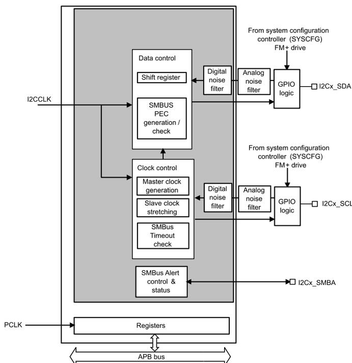
The block diagram illustrates the internal architecture of the I 2 C interface. At the bottom, an APB bus connects to a 'Registers' block, which is also connected to a 'PCLK' input. Above the registers are three main functional blocks: 'Data control', 'Clock control', and 'SMBus Alert control & status'. The 'Data control' block contains a 'Shift register' and 'SMBus PEC generation / check'. The 'Clock control' block contains 'Master clock generation', 'Slave clock stretching', and 'SMBus Timeout check'. The 'SMBus Alert control & status' block is connected to the 'I2Cx_SMBA' pin. The 'Data control' and 'Clock control' blocks are connected to 'Digital noise filter' blocks, which in turn connect to 'Analog noise filter' blocks. These analog filters connect to 'GPIO logic' blocks that drive the external pins 'I2Cx_SDA' and 'I2Cx_SCL'. These pins are also connected to 'From system configuration controller (SYSCFG) FM+ drive' inputs. The 'I2CCLK' input is connected to the 'Clock control' block.
The I 2 C is clocked by an independent clock source which allows the I 2 C to operate independently from the PCLK frequency.
This independent clock source is a fixed 16-MHz clock. Refer to Section 6: Reset and clock controller (RCC) for more details.
I 2 C I/Os supports 20 mA output current drive for fast-mode plus operation. This is enabled by setting the driving capability control bits for SCL and SDA in Section 8.2.3: I2C Fast-Mode Plus pin capability control register (I2C_FMP_CTRL) .
21.4.2 I 2 C clock requirements
The I 2 C kernel is clocked by I2CCLK.
The I2CCLK period \( t_{I2CCLK} \) must respect the following conditions:
with:
\( t_{LOW} \) : SCL low time and \( t_{HIGH} \) : SCL high time
\( t_{filters} \) : when enabled, sum of the delays brought by the analog filter and by the digital filter. Analog filter delay is maximum 260 ns. Digital filter delay is \( DNF \times t_{I2CCLK} \) .
The PCLK clock period \( t_{PCLK} \) must respect the following condition:
with \( t_{SCL} \) : SCL period.
21.4.3 Mode selection
The interface can operate in one of the four following modes:
- • Target transmitter
- • Target receiver
- • Controller transmitter
- • Controller receiver
By default, it operates in target mode. The interface automatically switches from target to controller when it generates a START condition, and from controller to target if an arbitration loss or a STOP generation occurs, allowing multicontroller capability.
Communication flow
In controller mode, the I 2 C interface initiates a data transfer and generates the clock signal. A serial data transfer always begins with a START condition and ends with a STOP condition. Both START and STOP conditions are generated in controller mode by software.
In target mode, the interface is capable of recognizing its own addresses (7 or 10-bit), and the general call address. The general call address detection can be enabled or disabled by software. The reserved SMBus addresses can also be enabled by software.
Data and addresses are transferred as 8-bit bytes, MSB first. The first byte(s) following the START condition contain the address (one in 7-bit mode, two in 10-bit mode). The address is always transmitted in controller mode.
A 9 th clock pulse follows the 8 clock cycles of a byte transfer, during which the receiver must send an acknowledge bit to the transmitter. Refer to the following figure.
Figure 95. I 2 C bus protocol
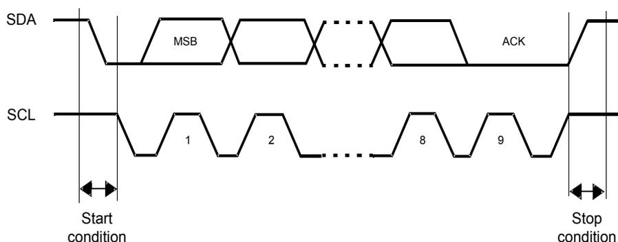
Acknowledge can be enabled or disabled by software. The I 2 C interface addresses can be selected by software.
21.4.4
I 2 C initialization
Enabling and disabling the peripheral
The I 2 C peripheral clock must be configured and enabled in the clock controller (refer to Section 6: Reset and clock controller (RCC) ).
Then the I 2 C can be enabled by setting the PE bit in the I2C_CR1 register. When the I 2 C is disabled (PE=0), the I 2 C performs a software reset. Refer to Section 21.4.5: Software reset for more details.
Noise filters
Before you enable the I 2 C peripheral by setting the PE bit in the I2C_CR1 register, you must configure the noise filters, if needed. By default, an analog noise filter is present on the SDA and SCL inputs. This analog filter is compliant with the I 2 C specification which requires the suppression of spikes with a pulse width up to 50 ns in fast-mode and fast-mode plus. You can disable this analog filter by setting the ANFOFF bit, and/or select a digital filter by configuring the DNF[3:0] bit in the I2C_CR1 register.
When the digital filter is enabled, the level of the SCL or the SDA line is internally changed only if it remains stable for more than DNF x I2CCLK periods. This allows spikes to be suppressed with a programmable length of 1 to 15 I2CCLK periods.
Caution: Changing the filter configuration is not allowed when the I 2 C is enabled.
I 2 C timings
The timings must be configured in order to guarantee a correct data hold and set-up time, used in controller and target modes. This is done by programming the PRESC[3:0], SCLDEL[3:0] and SDADEL[3:0] bits in the I2C_TIMINGR register.
Figure 96. Setup and hold timings
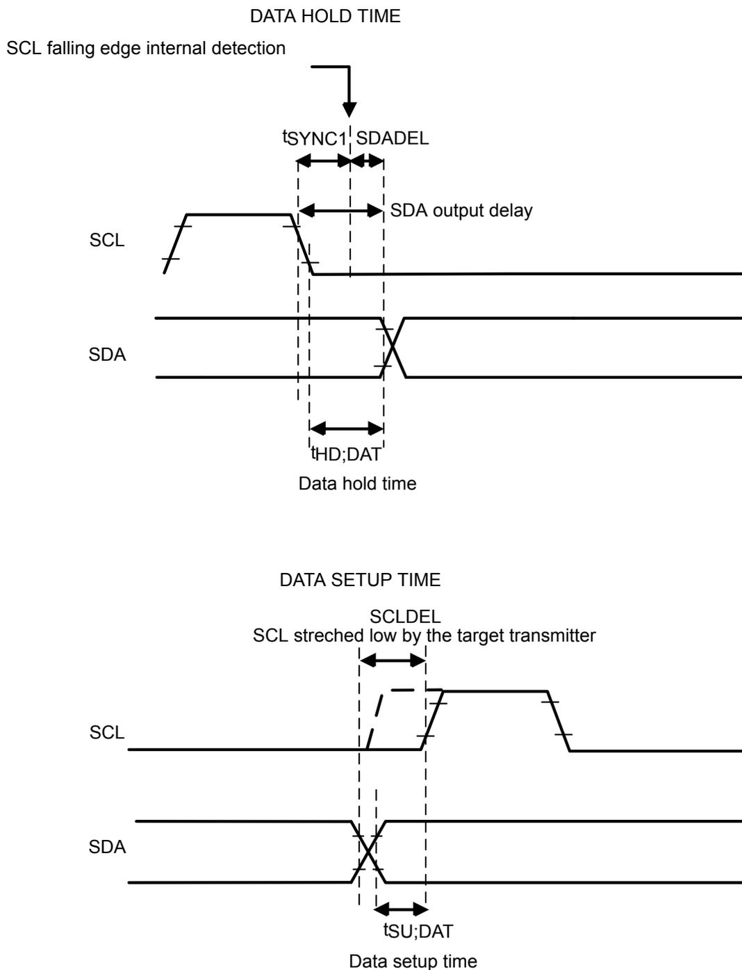
DATA HOLD TIME
SCL falling edge internal detection
SCL
SDA
\( t_{SYNC1} \) \( SDADEL \)
SDA output delay
\( t_{HD;DAT} \)
Data hold time
DATA SETUP TIME
SCLDEL
SCL stretched low by the target transmitter
SCL
SDA
\( t_{SU;DAT} \)
Data setup time
- When the SCL falling edge is internally detected, a delay is inserted before sending SDA output. This delay is
\( t_{SDADEL} \) and impacts the hold time \( t_{HD;DAT} \) .
The total SDA output delay is:
\( t_{SYNC1} \) duration depends on these parameters:
- SCL falling slope
- When enabled, input delay \( t_{SYNC1} \) brought by the analog filter: \( t_{AF(min)} < t_{AF} < t_{AF(max)} \) ns.
- When enabled, input delay brought by the digital filter: \( t_{DNF} = DNF \times t_{I2CCLK} \)
- Delay due to SCL synchronization to I2CCLK clock (2 to 3 I2CCLK periods)
In order to bridge the undefined region of the SCL falling edge, you must program SDADEL in such a way that:
Note: \( t_{AF(min)} \) / \( t_{AF(max)} \) are part of the equation only when the analog filter is enabled. Refer to device datasheet for \( t_{AF} \) values.
The maximum \( t_{HD;DAT} \) could be 3.45 µs, 0.9 µs and 0.45 µs for standard-mode, fast-mode and fast-mode plus, but must be less than the maximum of \( t_{VD;DAT} \) by a transition time. This maximum must only be met if the device does not stretch the LOW period ( \( t_{LOW} \) ) of the SCL signal. If the clock stretches the SCL, the data must be validated by the set-up time before it releases the clock.
The SDA rising edge is usually the worst case, so in this case the previous equation becomes:
Note: This condition can be violated when NOSTRETCH=0, because the device stretches SCL low to guarantee the set-up time, according to the SCLDEL value.
Refer to Table 86. I 2 C-SMBUS specification data setup and hold times for \( t_r \) , \( t_f \) , \( t_{HD;DAT} \) and \( t_{VD;DAT} \) standard values.
- After sending SDA output, SCL line is kept at low level during the set-up time. This set-up time is \( t_{SCLDEL} = (SCLDEL+1) \times t_{PRESC} \) where \( t_{PRESC} = (PRESC+1) \times t_{I2CCLK} \) . \( t_{SCLDEL} \) impacts the set-up time \( t_{SU;DAT} \) .
In order to bridge the undefined region of the SDA transition (rising edge usually worst case), you must program SCLDEL in such a way that:
Refer to Table 86. I 2 C-SMBUS specification data setup and hold times for \( t_r \) and \( t_{SU;DAT} \) standard values.
The SDA and SCL transition time values to be used are the ones in the application. Using the maximum values from the standard increases the constraints for the SDADEL and SCLDEL calculation, but ensures the feature whatever the application.
Table 86. I 2 C-SMBUS specification data setup and hold times
| Symbol | Parameter | Standard-mode (Sm) | Fast-mode (Fm) | Fast-mode Plus (Fm+) | SMBUS | Unit | ||||
|---|---|---|---|---|---|---|---|---|---|---|
| Min. | Max. | Min. | Max. | Min. | Max. | Min. | Max. | |||
| \( t_{HD;DAT} \) | Data hold time | 0 | - | 0 | - | 0 | - | 0.3 | - | µs |
| \( t_{VD;DAT} \) | Data valid time | - | 3.45 | - | 0.9 | - | 0.45 | - | - | µs |
| \( t_{SU;DAT} \) | Data set-up time | 250 | - | 100 | - | 50 | - | 250 | - | ns |
| \( t_r \) | Rise time of both SDA and SCL signals | - | 1000 | - | 300 | - | 120 | - | 1000 | ns |
| \( t_f \) | Fall time of both SDA and SCL signals | - | 300 | - | 300 | - | 120 | - | 300 | ns |
Additionally, in controller mode, the SCL clock high and low levels must be configured by programming the PRESC[3:0], SCLH[7:0] and SCLL[7:0] bits in the I2C_TIMINGR register.
- • When the SCL falling edge is internally detected, a delay is inserted before releasing the SCL output. This delay is \( t_{SCLL} = (SCLL+1) \times t_{PRESC} \) where \( t_{PRESC} = (PRESC+1) \times t_{I2CCLK} \) .
\( t_{SCLL} \) impacts the SCL low time \( t_{LOW} \) .
- • When the SCL rising edge is internally detected, a delay is inserted before forcing the SCL output to low level. This delay is \( t_{SCLH} = (SCLH+1) \times t_{PRESC} \) where \( t_{PRESC} = (PRESC+1) \times t_{I2CCLK} \) . \( t_{SCLH} \) impacts the SCL high time \( t_{HIGH} \) .
Refer to Section 21.4.8: I2C controller mode for more details.
Caution: Changing the timing configuration is not allowed when the I 2 C is enabled.
The I 2 C target NOSTRETCH mode must also be configured before enabling the peripheral.
Caution: Changing the NOSTRETCH configuration is not allowed when the I 2 C is enabled.
Figure 97. I 2 C initialization flowchart
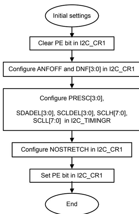
graph TD
    A([Initial settings]) --> B[Clear PE bit in I2C_CR1]
    B --> C[Configure ANFOFF and DNF[3:0] in I2C_CR1]
    C --> D["Configure PRESC[3:0],
SDADEL[3:0], SCLDEL[3:0], SCLH[7:0],
SCLL[7:0] in I2C_TIMINGR"]
    D --> E[Configure NOSTRETCH in I2C_CR1]
    E --> F[Set PE bit in I2C_CR1]
    F --> G([End])
21.4.5 Software reset
A software reset can be performed by clearing the PE bit in the I2C_CR1 register. In that case I 2 C lines SCL and SDA are released. Internal state machines are reset and communication control bits, as well as status bits come back to their reset value. The configuration registers are not impacted.
Here is the list of impacted register bits:
- 1. I2C_CR2 register: START, STOP, NACK
- 2. I2C_ISR register: BUSY, TXE, TXIS, RXNE, ADDR, NACKF, TCR, TC, STOPF, BERR, ARLO, OVR
- and in addition when the SMBus feature is supported:
- 1. I2C_CR2 register: PECBYTE
- 2. I2C_ISR register: PECERR, TIMEOUT, ALERT
PE must be kept low during at least 3 APB clock cycles in order to perform the software reset. This is ensured by writing the following software sequence: - Write PE=0 - Check PE=0 - Write PE=1.
21.4.6 Data transfer
The data transfer is managed through transmit and receive data registers and a shift register.
Reception
The SDA input fills the shift register. After the 8 th SCL pulse (when the complete data byte is received), the shift register is copied into the I2C_RXDR register if it is empty (RXNE=0). If RXNE=1, meaning that the previous received data byte has not yet been read, the SCL line is stretched low until I2C_RXDR is read. The stretch is inserted between the 8 th and 9 th SCL pulse (before the acknowledge pulse).
Figure 98. Data reception
The diagram shows the timing for data reception. The SCL line is a periodic clock. The Shift register contains 'xx', 'data1', 'xx', 'data2', 'xx'. The RXNE line is high when the shift register is not empty. The I2C_RXDR register contains 'data0', 'data1', 'data2'. Arrows show data being read from the shift register to I2C_RXDR ('rd data0', 'rd data1') when RXNE is high and an ACK pulse is received. A blue line on the SCL signal indicates a stretch between the 8th and 9th pulses.
Transmission
If the I2C_TXDR register is not empty (TXE=0), its content is copied into the shift register after the 9 th SCL pulse (the acknowledge pulse). Then the shift register content is shifted out on the SDA line. If TXE=1, meaning that no data is written yet in I2C_TXDR, SCL line is stretched low until I2C_TXDR is written. The stretch is done after the 9 th SCL pulse.
Figure 99. Data transmission
The diagram shows the timing for data transmission. The SCL line is a periodic clock. The Shift register contains 'xx', 'data1', 'xx', 'data2', 'xx'. The TXE line is high when the shift register is empty. The I2C_TXDR register contains 'data0', 'data1', 'data2'. Arrows show data being written from I2C_TXDR to the shift register ('wr data1', 'wr data2') when TXE is high and an ACK pulse is received. A blue line on the SCL signal indicates a stretch after the 9th pulse.
Hardware transfer management
The I 2 C has a byte counter embedded in hardware in order to manage byte transfer and to close the communication in various modes such as:
- • NACK, STOP and ReSTART generation in controller mode
- • ACK control in target receiver mode
- • PEC generation/checking when SMBus feature is supported
The byte counter is always used in controller mode. By default it is disabled in target mode, but it can be enabled by software by setting the SBC (target byte control) bit in the I2C_CR2 register.
The number of bytes to be transferred is programmed in the NBBYTES[7:0] bit field in the I2C_CR2 register. If the number of bytes to be transferred (NBBYTES) is greater than 255, or if a receiver wants to control the acknowledge value of a received data byte, the reload mode must be selected by setting the RELOAD bit in the I2C_CR2 register. In this mode, TCR flag is set when the number of bytes programmed in NBBYTES has been transferred, and an interrupt is generated if TCIE is set. SCL is stretched as long as TCR flag is set. TCR is cleared by software when NBBYTES is written to a non-zero value.
When the NBBYTES counter is reloaded with the last number of bytes, RELOAD bit must be cleared.
When RELOAD=0 in controller mode, the counter can be used in 2 modes:
- • Automatic end mode (AUTOEND = '1' in the I2C_CR2 register). In this mode, the controller automatically sends a STOP condition once the number of bytes programmed in the NBBYTES[7:0] bit field has been transferred.
- • Software end mode (AUTOEND = '0' in the I2C_CR2 register). In this mode, software action is expected once the number of bytes programmed in the NBBYTES[7:0] bit field has been transferred; the TC flag is set and an interrupt is generated if the TCIE bit is set. The SCL signal is stretched as long as the TC flag is set. The TC flag is cleared by software when the START or STOP bit is set in the I2C_CR2 register. This mode must be used when the controller wants to send a RESTART condition.
Caution: The AUTOEND bit has no effect when the RELOAD bit is set.
Table 87. I 2 C configurable table
| Function | SBC bit | RELOAD bit | AUTOEND bit |
|---|---|---|---|
| Controller Tx/Rx NBBYTES + STOP | x | 0 | 1 |
| Controller Tx/Rx + NBBYTES + RESTART | x | 0 | 0 |
| Target Tx/Rx all received bytes ACKed | 0 | x | x |
| Target Rx with ACK control | 1 | 1 | x |
21.4.7 I2C target mode
I 2 C target initialization
In order to work in target mode, you must enable at least one target address. Two registers, I2C_OAR1 and I2C_OAR2, are available in order to program the target own addresses OA1 and OA2.
- • OA1 can be configured either in 7-bit mode (by default) or in 10-bit addressing mode by setting the OA1MODE bit in the I2C_OAR1 register.
OA1 is enabled by setting the OA1EN bit in the I2C_OAR1 register. - • If additional target addresses are required, you can configure the 2
nd
target address OA2. Up to 7 OA2 LSB can be masked by configuring the OA2MSK[2:0] bits in the I2C_OAR2 register. Therefore for OA2MSK configured from 1 to 6, only OA2[7:2], OA2[7:3], OA2[7:4], OA2[7:5], OA2[7:6] or OA2[7] are compared with the received address. As soon as OA2MSK is not equal to 0, the address comparator for OA2 excludes the I
2
C reserved addresses (0000 XXX and 1111 XXX), which are not acknowledged. If OA2MSK=7, all received 7-bit addresses are acknowledged (except reserved addresses). OA2 is always a 7-bit address.
These reserved addresses can be acknowledged if they are enabled by the specific enable bit, if they are programmed in the I2C_OAR1 or I2C_OAR2 register with OA2MSK=0.
OA2 is enabled by setting the OA2EN bit in the I2C_OAR2 register. - • The general call address is enabled by setting the GCEN bit in the I2C_CR1 register.
When the I 2 C is selected by one of its enabled addresses, the ADDR interrupt status flag is set, and an interrupt is generated if the ADDRIE bit is set.
By default, the target uses its clock stretching capability, which means that it stretches the SCL signal at low level when needed, in order to perform software actions. If the controller does not support clock stretching, the I 2 C must be configured with NOSTRETCH=1 in the I2C_CR1 register.
After receiving an ADDR interrupt, if several addresses are enabled you must read the ADDCODE[6:0] bits in the I2C_ISR register in order to check which address matched. DIR flag must also be checked in order to know the transfer direction.
Target clock stretching (NOSTRETCH = 0)
In default mode, the I 2 C target stretches the SCL clock in the following situations:
- • When the ADDR flag is set: the received address matches with one of the enabled target addresses. This stretch is released when the ADDR flag is cleared by software setting the ADDRCF bit.
- • In transmission, if the previous data transmission is completed and no new data is written in I2C_TXDR register, or if the first data byte is not written when the ADDR flag is cleared (TXE=1). This stretch is released when the data is written to the I2C_TXDR register.
- • In reception when the I2C_RXDR register is not read yet and a new data reception is completed. This stretch is released when I2C_RXDR is read.
- • When TCR = 1 in target byte Control mode, reload mode (SBC=1 and RELOAD=1), meaning that the last data byte has been transferred. This stretch is released when then TCR is cleared by writing a non-zero value in the NBBYTES[7:0] field.
- • After SCL falling edge detection, the I 2 C stretches SCL low during \( [(SDADEL+SCLDEL+1) \times (PRESC+1) + 1] \times tI2CCLK \) .
Target without clock stretching (NOSTRETCH = 1)
When NOSTRETCH = 1 in the I2C_CR1 register, the I 2 C target does not stretch the SCL signal.
- • The SCL clock is not stretched while the ADDR flag is set.
- • In transmission, the data must be written in the I2C_TXDR register before the first SCL pulse corresponding to its transfer occurs. If not, an underrun occurs, the OVR flag is set in the I2C_ISR register and an interrupt is generated if the ERRIE bit is set in the I2C_CR1 register. The OVR flag is also set when the first data transmission starts and the STOPF bit is still set (has not been cleared). Therefore, if you clear the STOPF flag of the previous transfer only after writing the first data to be transmitted in the next transfer, you ensure that the OVR status is provided, even for the first data to be transmitted.
- • In reception, the data must be read from the I2C_RXDR register before the 9 th SCL pulse (ACK pulse) of the next data byte occurs. If not an overrun occurs, the OVR flag is set in the I2C_ISR register and an interrupt is generated if the ERRIE bit is set in the I2C_CR1 register.
Target byte control mode
In order to allow byte ACK control in target reception mode, target byte control mode must be enabled by setting the SBC bit in the I2C_CR1 register. This is required to be compliant with SMBus standards.
Reload mode must be selected in order to allow byte ACK control in target reception mode (RELOAD=1). To get control of each byte, NBBYTES must be initialized to 0x1 in the ADDR interrupt subroutine, and reloaded to 0x1 after each received byte. When the byte is received, the TCR bit is set, stretching the SCL signal low between the 8 th and 9 th SCL pulses. You can read the data from the I2C_RXDR register, and then decide to acknowledge it or not by configuring the ACK bit in the I2C_CR2 register. The SCL stretch is released by programming NBBYTES to a non-zero value: the acknowledge or not- acknowledge is sent and the next byte can be received.
NBYTES can be loaded with a value greater than 0x1, and in this case, the reception flow is continuous during NBBYTES data reception.
Note: The SBC bit must be configured when the I 2 C is disabled, or when the target is not addressed, or when ADDR=1. The RELOAD bit value can be changed when ADDR=1, or when TCR=1.
Caution: Target byte control mode is not compatible with NOSTRETCH mode. Setting SBC when NOSTRETCH=1 is not allowed.
Figure 100. Target initialization flowchart
![Flowchart for Target initialization. Steps: Target initialization (oval) -> Initial settings (rectangle) -> Clear {OA1EN, OA2EN} in I2C_CR1 (rectangle) -> Configure {OA1[9:0], OA1MODE, OA1EN, OA2[6:0], OA2MSK[2:0], OA2EN, GCEN} (rectangle) -> Configure SBC in I2C_CR1* (rectangle) -> Enable interrupts and/or DMA in I2C_CR1 (rectangle) -> End (oval).](/RM0529-STM32WB05xZ/cf6ca8f1a86c81dccf05cb590811fa7e_img.jpg)
graph TD
    A([Target initialization]) --> B[Initial settings]
    B --> C[Clear {OA1EN, OA2EN} in I2C_CR1]
    C --> D["Configure {OA1[9:0], OA1MODE, OA1EN, OA2[6:0], OA2MSK[2:0], OA2EN, GCEN}"]
    D --> E[Configure SBC in I2C_CR1*]
    E --> F[Enable interrupts and/or DMA in I2C_CR1]
    F --> G([End])
*SBC must be set to support SMBus features
Target transmitter
A transmit interrupt status (TXIS) is generated when the I2C_TXDR register becomes empty. An interrupt is generated if the TXIE bit is set in the I2C_CR1 register.
The TXIS bit is cleared when the I2C_TXDR register is written with the next data byte to be transmitted.
When a NACK is received, the NACKF bit is set in the I2C_ISR register and an interrupt is generated if the NACKIE bit is set in the I2C_CR1 register. The target automatically releases the SCL and SDA lines in order to let the controller perform a STOP or a RESTART condition. The TXIS bit is not set when a NACK is received.
When a STOP is received and the STOPIE bit is set in the I2C_CR1 register, the STOPF flag is set in the I2C_ISR register and an interrupt is generated. In most applications, the SBC bit is usually programmed to '0'. In this case, If TXE = 0 when the target address is received (ADDR=1), you can choose either to send the content of the I2C_TXDR register as the first data byte, or to flush the I2C_TXDR register by setting the TXE bit in order to program a new data byte.
In target byte control mode (SBC=1), the number of bytes to be transmitted must be programmed in NBBYTES in the address match interrupt subroutine (ADDR=1). In this case, the number of TXIS events during the transfer corresponds to the value programmed in NBBYTES.
Caution: When NOSTRETCH=1, the SCL clock is not stretched while the ADDR flag is set, so you cannot flush the I2C_TXDR register content in the ADDR subroutine, in order to program the first data byte. The first data byte to be sent must be previously programmed in the I2C_TXDR register:
- • This data can be the data written in the last TXIS event of the previous transmission message
- • If this data byte is not the one to be sent, the I2C_TXDR register can be flushed by setting the TXE bit in order to program a new data byte. The STOPF bit must be cleared only after these actions, in order to guarantee that they are executed before the first data transmission starts, following the address acknowledge.
If STOPF is still set when the first data transmission starts, an underrun error is generated (the OVR flag is set).
If you need a TXIS event, (Transmit Interrupt or Transmit DMA request), you must set the TXIS bit in addition to the TXE bit, in order to generate a TXIS event.
Figure 101. Transfer sequence flowchart for I2C target transmitter, NOSTRETCH=0
graph TD;
    Start([Target transmission]) --> Init[Target initialization];
    Init --> AddrCheck{I2C_ISR.ADDR = 1?};
    AddrCheck -- No --> AddrCheck;
    AddrCheck -- Yes --> ReadAddr[Read ADDCODE and DIR in I2C_ISR
Optional: Set I2C_ISR.TXE = 1
Set I2C_ICR.ADDRCF];
    ReadAddr --> TxisCheck{I2C_ISR.TXIS = 1?};
    TxisCheck -- No --> TxisCheck;
    TxisCheck -- Yes --> WriteData[Write I2C_TXDR.TXDATA];
    WriteData --> TxisCheck;

    subgraph SCL_Stretched [SCL stretched]
    AddrCheck
    ReadAddr
    TxisCheck
    end
The flowchart describes the process for target transmission when clock stretching is enabled (NOSTRETCH=0). It starts with Target transmission followed by Target initialization . The system waits for I2C_ISR.ADDR = 1 . Once detected, it reads ADDCODE and DIR , optionally sets I2C_ISR.TXE = 1 , and sets I2C_ICR.ADDRCF . Then, it enters a loop waiting for I2C_ISR.TXIS = 1 to Write I2C_TXDR.TXDATA . A vertical arrow indicates that SCL is stretched from the address match until the first data is written.
Figure 102. Transfer sequence flowchart for I2C target transmitter, NOSTRETCH=1
graph TD;
    Start([Target transmission]) --> Init[Target initialization];
    Init --> TxisCheck{I2C_ISR.TXIS = 1?};
    Init --> StopfCheck{I2C_ISR.STOPF = 1?};

    TxisCheck -- No --> TxisCheck;
    TxisCheck -- Yes --> WriteData[Write I2C_TXDR.TXDATA];
    WriteData --> TxisCheck;

    StopfCheck -- No --> StopfCheck;
    StopfCheck -- Yes --> OptSet[Optional: Set I2C_ISR.TXE = 1
and I2C_ISR.TXIS=1];
    OptSet --> Stopcf[Set I2C_ICR.STOPCF];
The flowchart describes the process for target transmission when clock stretching is disabled (NOSTRETCH=1). After Target initialization , two parallel paths are followed. The left path handles data transmission by waiting for I2C_ISR.TXIS = 1 and then performing Write I2C_TXDR.TXDATA . The right path monitors for the stop condition: when I2C_ISR.STOPF = 1 , it optionally sets I2C_ISR.TXE = 1 and I2C_ISR.TXIS = 1 , then sets I2C_ICR.STOPCF .
Figure 103. Transfer bus diagram for I2C target transmitter
graph TD
    Start([Target reception]) --> Init[Target initialization]
    Init --> RXNE{I2C_ISR.RXNE = 1?}
    RXNE -- Yes --> Read[Read I2C_RXDR.RXDATA]
    Read --> RXNE
    RXNE -- No --> STOPF{I2C_ISR.STOPF = 1?}
    STOPF -- Yes --> StopCF[Set I2C_ICR.STOPCF]
    StopCF --> RXNE
    STOPF -- No --> RXNE
Target receiver
RXNE is set in I2C_ISR when the I2C_RXDR is full, and generates an interrupt if RXIE is set in I2C_CR1. RXNE is cleared when I2C_RXDR is read.
When a STOP is received and STOPIE is set in I2C_CR1, STOPF is set in I2C_ISR and an interrupt is generated.
Figure 104. Transfer sequence flowchart for target receiver with NOSTRETCH=0
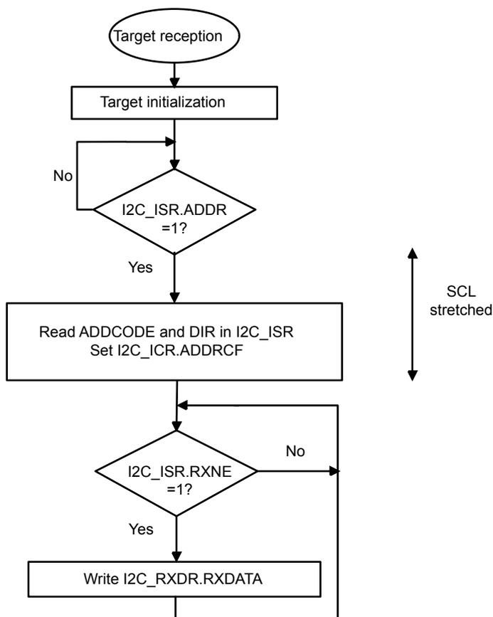
graph TD
    Start([Target reception]) --> Init[Target initialization]
    Init --> ADDR{I2C_ISR.ADDR = 1?}
    ADDR -- Yes --> ReadAddr[Read ADDCODE and DIR in I2C_ISR
Set I2C_ICR.ADDRCF]
    ReadAddr --> RXNE{I2C_ISR.RXNE = 1?}
    RXNE -- Yes --> Write[Write I2C_RXDR.RXDATA]
    Write --> RXNE
    RXNE -- No --> ADDR
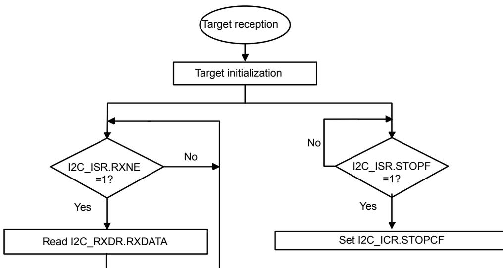
Figure 105. Transfer sequence flowchart for target receiver with NOSTRETCH=1
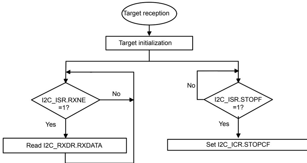
graph TD
    Start([Target reception]) --> Init[Target initialization]
    Init --> RXNE{I2C_ISR.RXNE = 1?}
    RXNE -- Yes --> Read[Read I2C_RXDR.RXDATA]
    Read --> RXNE
    RXNE -- No --> STOPF{I2C_ISR.STOPF = 1?}
    STOPF -- Yes --> Stop[Set I2C_ICR.STOPCF]
    STOPF -- No --> RXNE
Figure 106. Transfer bus diagrams for I2C target receiver
Example I2C target receiver 3 bytes, NOSTRETCH=0:
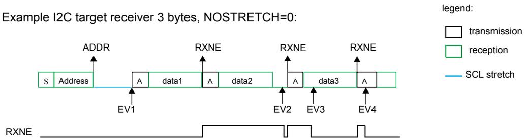
bus sequence: S Address A data1 A data2 A data3 A [ ]
events: EV1(ADDR) EV2(RXNE) EV3(RXNE) EV4(RXNE)
RXNE signal: [Pulse] [Pulse] [Pulse]
legend:
- transmission
- reception
- SCL stretch
- EV1: ADDR ISR: check ADDCODE and DIR, set ADDRCF
- EV2: RXNE ISR: rd data1
- EV3: RXNE ISR: rd data2
- EV4: RXNE ISR: rd data3
Example I2C target receiver 3 bytes, NOSTRETCH=1:
bus sequence: S Address A data1 data2 data3 A P
events: EV1(RXNE) EV2(RXNE) EV3(RXNE)
RXNE signal: [Pulse] [Pulse] [Pulse]
legend:
- transmission
- reception
- SCL stretch
- EV1: RXNE ISR: rd data1
- EV2: RXNE ISR: rd data2
- EV3: RXNE ISR: rd data3
- EV4: STOPF ISR: set STOPCF
21.4.8 I2C controller mode
I2C controller initialization
Before enabling the peripheral, the I 2 C controller clock must be configured by setting the SCLH and SCLL bits in the I2C_TIMINGR register.
A clock synchronization mechanism is implemented in order to support multi-controller environment and target clock stretching.
In order to allow clock synchronization:
- • The low level of the clock is counted using the SCLL counter, starting from the SCL low level internal detection.
- • The high level of the clock is counted using the SCLH counter, starting from the SCL high level internal detection.
The I 2 C detects its own SCL low level after a \( t_{\text{SYNC1}} \) delay depending on the SCL falling edge, SCL input noise filters (analog + digital) and SCL synchronization to the I2CxCLK clock. The I 2 C releases SCL to high level once the SCLL counter reaches the value programmed in the SCLL[7:0] bits in the I2C_TIMINGR register.
The I 2 C detects its own SCL high level after a \( t_{\text{SYNC2}} \) delay depending on the SCL rising edge, SCL input noise filters (analog + digital) and SCL synchronization to I2CxCLK clock. The I 2 C ties SCL to low level once the SCLH counter reaches the value programmed in the SCLH[7:0] bits in the I2C_TIMINGR register.
Consequently the controller clock period is:
The duration of \( t_{\text{SYNC1}} \) depends on these parameters:
- • SCL falling slope
- • When enabled, input delay induced by the analog filter
- • When enabled, input delay induced by the digital filter: \( \text{DNF} \times t_{\text{I2CCLK}} \)
- • Delay due to SCL synchronization with I2CCLK clock (2 to 3 I2CCLK periods).
The duration of \( t_{\text{SYNC2}} \) depends on these parameters:
- • SCL rising slope
- • When enabled, input delay induced by the analog filter
- • When enabled, input delay induced by the digital filter: \( \text{DNF} \times t_{\text{I2CCLK}} \)
- • Delay due to SCL synchronization with I2CCLK clock (2 to 3 I2CCLK periods).
Figure 107. Controller clock generation
SCL controller clock generation
SCL controller clock synchronization
Caution: In order to be I 2 C or SMBus compliant, the controller clock must respect the timings given below:
Table 88. I 2 C-SMBUS specification clock timings
| Symbol | Parameter | Standard-mode (Sm) | Fast-mode (Fm) | Fast-mode Plus (Fm+) | SMBUS | Unit | ||||
|---|---|---|---|---|---|---|---|---|---|---|
| Min. | Max. | Min. | Max. | Min. | Max. | Min. | Max. | |||
| f SCL | SCL clock frequency | 100 | 400 | 1000 | 100 | kHz | ||||
| t HD:STA | Hold time (repeated) START condition | 4.0 | - | 0.6 | - | 0.26 | - | 4.0 | - | µs |
| t SU:STA | Set-up time for a repeated START condition | 4.7 | - | 0.6 | - | 0.26 | - | 4.7 | - | µs |
| t SU:STO | Set-up time for STOP condition | 4.0 | - | 0.6 | - | 0.26 | - | 4.0 | - | µs |
| t BUF | Bus free time between a STOP and START condition | 4.7 | - | 1.3 | - | 0.5 | - | 4.7 | - | µs |
| t LOW | Low period of the SCL clock | 4.7 | - | 1.3 | - | 0.5 | - | 4.7 | - | µs |
| t HIGH | Period of the SCL clock | 4.0 | - | 0.6 | - | 0.26 | - | 4.0 | 50 | µs |
| t r | Rise time of both SDA and SCL signals | - | 1000 | - | 300 | - | 120 | - | 1000 | ns |
| t f | Fall time of both SDA and SCL signals | - | 300 | - | 300 | - | 120 | - | 300 | ns |
Note: SCLL is also used to generate the t BUF and t SU:STA timings.
SCLH is also used to generate the t HD:STA and t SU:STO timings.
Refer to Section 21.4.9: I2C_TIMINGR register configuration examples for examples of I2C_TIMINGR settings vs. I2CCLK frequency.
Controller communication initialization (address phase)
In order to initiate the communication, you must program the following parameters for the addressed target in the I2C_CR2 register:
- • Addressing mode (7-bit or 10-bit): ADD10
- • Target address to be sent: SADD[9:0]
- • Transfer direction: RD_WRN
- • In case of 10-bit address read: HEAD10R bit. HEAD10R must be configured to indicate if the complete address sequence must be sent, or only the header in case of a direction change.
- • The number of bytes to be transferred: NBYTES[7:0]. If the number of bytes is equal to or greater than 255 bytes, NBYTES[7:0] must initially be filled with 0xFF.
You must then set the START bit in the I2C_CR2 register. Changing all the above bits is not allowed when START bit is set.
Then the controller automatically sends the START condition followed by the target address as soon as it detects that the bus is free (BUSY = 0) and after a delay of t BUF .
In case of an arbitration loss, the controller automatically switches back to target mode and can acknowledge its own address if it is addressed as a target.
Note: The START bit is reset by hardware when the target address has been sent on the bus, whatever the received acknowledge value. The START bit is also reset by hardware if an arbitration loss occurs. If the I 2 C is addressed as a target (ADDR=1) while the START bit is set, the I 2 C switches to target mode and the START bit is cleared when the ADDRCF bit is set.
Note: The same procedure is applied for a repeated start condition. In this case BUSY=1.
Figure 108. Controller initialization flowchart
graph TD
    A([Controller initialization]) --> B[Initial settings]
    B --> C[Enable interrupts and/or DMA in I2C_CR1]
    C --> D([End])
Initialization of a controller receiver addressing a 10-bit address target
- • If the target address is in 10-bit format, you can choose to send the complete read sequence by clearing the HEAD10R bit in the I2C_CR2 register. In this case the controller automatically sends the following complete sequence after the START bit is set: (Re)Start + target address 10-bit header Write + target address 2nd byte + REStart + target address 10-bit header Read
- • If the controller addresses a 10-bit address target, transmits data to this target and then reads data from the same target, a controller transmission flow must be done first. Then a repeated start is set with the 10 bit target address configured with HEAD10R=1. In this case the controller sends this sequence: ReStart + target address 10-bit header Read.
Figure 109. 10-bit address read access with HEAD10R=1
Controller transmitter
In the case of a write transfer, the TXIS flag is set after each byte transmission, after the 9 th SCL pulse when an ACK is received.
A TXIS event generates an interrupt if the TXIE bit is set in the I2C_CR1 register. The flag is cleared when the I2C_TXDR register is written with the next data byte to be transmitted.
The number of TXIS events during the transfer corresponds to the value programmed in NBBYTES[7:0]. If the total number of data bytes to be sent is greater than 255, reload mode must be selected by setting the RELOAD bit in the I2C_CR2 register. In this case, when NBBYTES data have been transferred, the TCR flag is set and the SCL line is stretched low until NBBYTES[7:0] is written to a non-zero value.
The TXIS flag is not set when a NACK is received.
- • When RELOAD=0 and NBYTES data have been transferred:
- – In automatic end mode (AUTOEND=1), a STOP is automatically sent.
- – In software end mode (AUTOEND=0), the TC flag is set and the SCL line is stretched low in order to perform software actions:
A RESTART condition can be requested by setting the START bit in the I2C_CR2 register with the proper target address configuration, and number of bytes to be transferred. Setting the START bit clears the TC flag and the START condition is sent on the bus.
A STOP condition can be requested by setting the STOP bit in the I2C_CR2 register. Setting the STOP bit clears the TC flag and the STOP condition is sent on the bus.
- • If a NACK is received: the TXIS flag is not set, and a STOP condition is automatically sent after the NACK reception. the NACKF flag is set in the I2C_ISR register, and an interrupt is generated if the NACKIE bit is set.
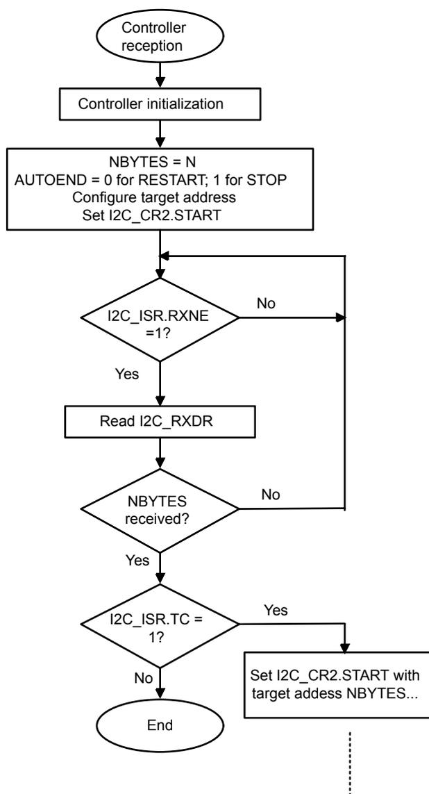
Figure 110. Transfer sequence flowchart for I2C controller transmitter for N 255 bytes
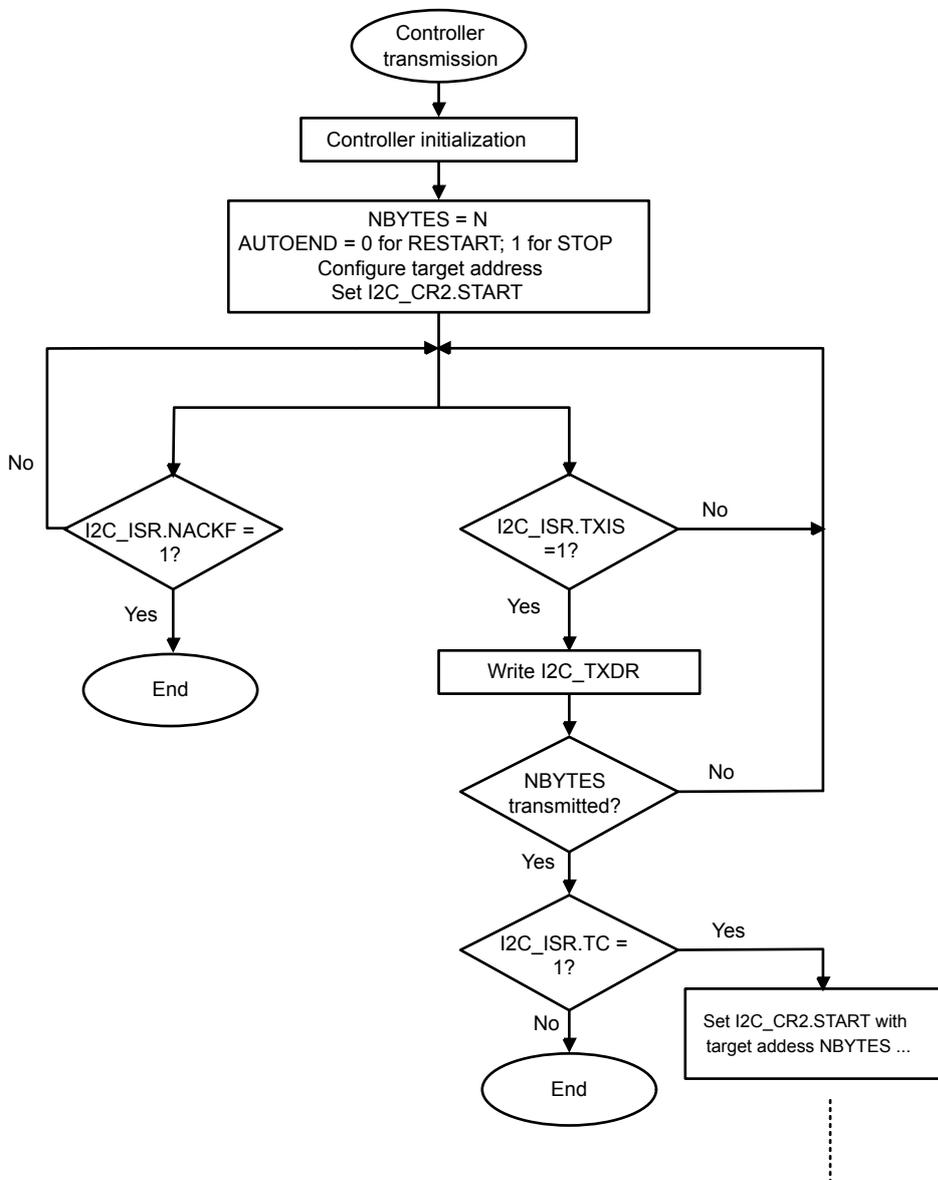
graph TD
    Start([Controller transmission]) --> Init[Controller initialization]
    Init --> Config["NBYTES = N
AUTOEND = 0 for RESTART; 1 for STOP
Configure target address
Set I2C_CR2.START"]
    Config --> LoopStart(( ))
    LoopStart --> TXIS{I2C_ISR.TXIS = 1?}
    TXIS -- No --> NACKF{I2C_ISR.NACKF = 1?}
    NACKF -- Yes --> End1([End])
    NACKF -- No --> LoopStart
    TXIS -- Yes --> Write[Write I2C_TXDR]
    Write --> Transmitted{NBYTES transmitted?}
    Transmitted -- No --> LoopStart
    Transmitted -- Yes --> TC{I2C_ISR.TC = 1?}
    TC -- Yes --> SetStart["Set I2C_CR2.START with
target address NBYTES ..."]
    TC -- No --> End2([End])
    SetStart -.-> DashedLine[⋮]
    End2 -.-> DashedLine
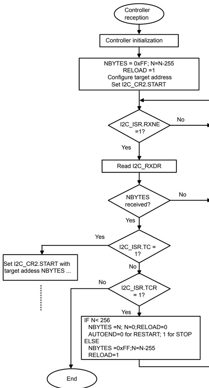
Figure 111. Transfer sequence flowchart for I2C controller transmitter for N>255 bytes
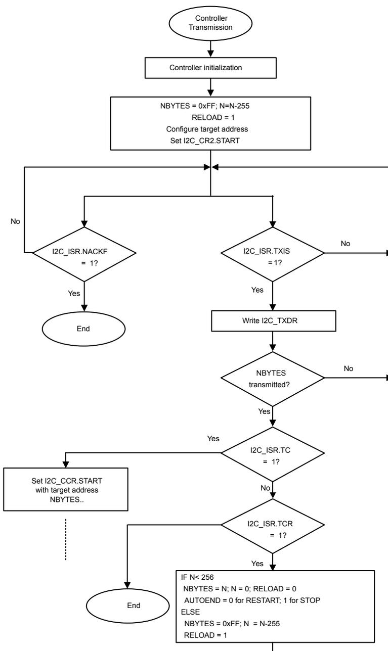
graph TD
    Start([Controller Transmission]) --> Init[Controller initialization]
    Init --> Config["NBYTES = 0xFF; N=N-255
RELOAD = 1
Configure target address
Set I2C_CR2.START"]
    Config --> LoopStart(( ))
    LoopStart --> NACKF{I2C_ISR.NACKF
= 1?}
    LoopStart --> TXIS{I2C_ISR.TXIS
= 1?}
    NACKF -- Yes --> End1([End])
    NACKF -- No --> LoopStart
    TXIS -- Yes --> Write[Write I2C_TXDR]
    TXIS -- No --> LoopStart
    Write --> Transmitted{NBYTES
transmitted?}
    Transmitted -- Yes --> TC{I2C_ISR.TC
= 1?}
    Transmitted -- No --> LoopStart
    TC -- Yes --> CCR[Set I2C_CCR.START
with target address
NBYTES..]
    TC -- No --> TCR{I2C_ISR.TCR
= 1?}
    TCR -- Yes --> Logic["IF N < 256
NBYTES = N; N = 0; RELOAD = 0
AUTOEND = 0 for RESTART; 1 for STOP
ELSE
NBYTES = 0xFF; N = N-255
RELOAD = 1"]
    TCR -- No --> LoopStart
    CCR -.-> End2([End])
    Logic --> End2
Figure 112. Transfer bus diagrams for I2C controller transmitter
Example I2C controller transmitter 2 bytes, automatic end mode (STOP)
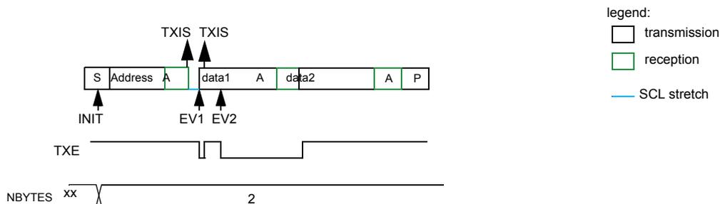
The diagram illustrates the transfer bus for an I2C controller transmitter in automatic end mode (STOP). The sequence of events is as follows:
- INIT : Program target address, program NBBYTES = 2, AUTOEND=1, set START. The bus shows a Start condition (S) followed by an Address.
- EV1 : TXIS ISR: write data1. The bus shows data1 being transmitted.
- EV2 : TXIS ISR: write data2. The bus shows data2 being transmitted.
- P : Stop condition. The bus shows a Stop condition (P).
INIT: program target address, program NBBYTES = 2, AUTOEND=1, set START
EV1: TXIS ISR: wr data1
EV2: TXIS ISR: wr data2
Example I2C controller transmitter 2 bytes, software end (RESTART)
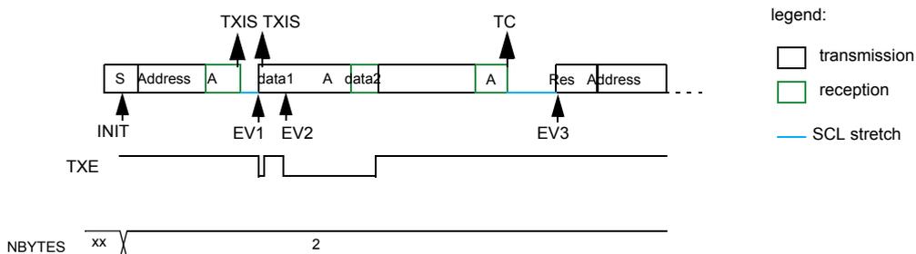
The diagram illustrates the transfer bus for an I2C controller transmitter in software end mode (RESTART). The sequence of events is as follows:
- INIT : program target address, program NBBYTES = 2, AUTOEND=0, set START. The bus shows a Start condition (S) followed by an Address.
- EV1 : TXIS ISR: write data1. The bus shows data1 being transmitted.
- EV2 : TXIS ISR: write data2. The bus shows data2 being transmitted.
- EV3 : TC ISR: program target address, program NBBYTES = N, set START. The bus shows a TC (transfer complete) condition followed by a Restart condition (Res) and a new Address.
INIT: program target address, program NBBYTES = 2, AUTOEND=0, set START
EV1: TXIS ISR: wr data1
EV2: TXIS ISR: wr data2
EV3: TC ISR: program target address, program NBBYTES = N, set START
Controller receiver
In the case of a read transfer, the RXNE flag is set after each byte reception, after the 8th SCL pulse. An RXNE event generates an interrupt if the RXIE bit is set in the I2C_CR1 register. The flag is cleared when I2C_RXDR is read.
If the total number of data bytes to be received is greater than 255, reload mode must be selected by setting the RELOAD bit in the I2C_CR2 register. In this case, when NBBYTES[7:0] data have been transferred, the TCR flag is set and the SCL line is stretched low until NBBYTES[7:0] is written to a non-zero value.
- When RELOAD=0 and NBBYTES[7:0] data have been transferred:
- In automatic end mode (AUTOEND=1), a NACK and a STOP are automatically sent after the last received byte
- In software end mode (AUTOEND=0), a NACK is automatically sent after the last received byte, the TC flag is set and the SCL line is stretched low in order to allow software actions:
A RESTART condition can be requested by setting the START bit in the I2C_CR2 register with the proper target address configuration, and number of bytes to be transferred. Setting the START bit clears the TC flag and the START condition, followed by target address, are sent on the bus.
A STOP condition can be requested by setting the STOP bit in the I2C_CR2 register. Setting the STOP bit clears the TC flag and the STOP condition is sent on the bus.
Figure 113. Transfer sequence flowchart for I 2 C controller receiver for N>255 bytes
graph TD
    Start([Controller reception]) --> Init[Controller initialization]
    Init --> Config["NBYTES = N
AUTOEND = 0 for RESTART; 1 for STOP
Configure target address
Set I2C_CR2.START"]
    Config --> RXNE{I2C_ISR.RXNE = 1?}
    RXNE -- No --> RXNE
    RXNE -- Yes --> Read[Read I2C_RXDR]
    Read --> Received{NBYTES received?}
    Received -- No --> RXNE
    Received -- Yes --> TC{I2C_ISR.TC = 1?}
    TC -- Yes --> SetStart["Set I2C_CR2.START with
target address NBYTES..."]
    TC -- No --> End([End])
    SetStart -.-> Dots[⋮]
Figure 114. Transfer sequence flowchart for I 2 C controller receiver for N >255 bytes
graph TD
    Start([Controller reception]) --> Init[Controller initialization]
    Init --> Setup["NBYS = 0xFF; N=N-255
RELOAD =1
Configure target address
Set I2C_CR2.START"]
    Setup --> RXNE{"I2C_ISR.RXNE =1?"}
    RXNE -- No --> NBYS_RECV{"NBYS received?"}
    RXNE -- Yes --> ReadRXDR[Read I2C_RXDR]
    ReadRXDR --> NBYS_RECV
    NBYS_RECV -- No --> RXNE
    NBYS_RECV -- Yes --> TC{"I2C_ISR.TC = 1?"}
    TC -- Yes --> SetStart["Set I2C_CR2.START with
target address NBYS ..."]
    TC -- No --> TCR{"I2C_ISR.TCR = 1?"}
    TCR -- Yes --> EndCond["IF N < 256
NBYS = N; N=0; RELOAD=0
AUTOEND=0 for RESTART; 1 for STOP
ELSE
NBYS = 0xFF; N=N-255
RELOAD=1"]
    SetStart --> End([End])
    EndCond --> End
Figure 115. Transfer bus diagrams for I 2 C controller receiver
Example I2C controller receiver 2 bytes, automatic end mode (STOP)
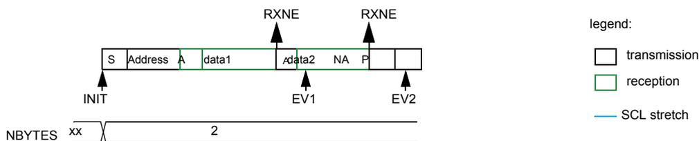
The diagram shows the following sequence of events:
- INIT : Start condition (S) and target address.
- A : Address Acknowledge.
- data1 : First data byte received. RXNE flag is set at the end of reception.
- A : Acknowledge for data1.
- data2 : Second data byte received. RXNE flag is set at the end of reception.
- NA : Not Acknowledge for data2.
- P : Stop condition.
- EV1 : RXNE ISR: rd data1.
- EV2 : RXNE ISR: rd data2.
NBYTES register: xx | 2
legend:
- transmission (white box)
- reception (green box)
- SCL stretch (blue line)
INIT: program target address, program NBYTES = 2, AUTOEND=1, set START
EV1: RXNE ISR: rd data1
EV2: RXNE ISR: rd data2
Example I2C controller receiver 2 bytes, software end mode (RESTART)
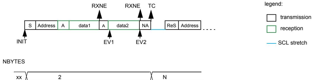
The diagram shows the following sequence of events:
- INIT : Start condition (S) and target address.
- A : Address Acknowledge.
- data1 : First data byte received. RXNE flag is set at the end of reception.
- A : Acknowledge for data1.
- data2 : Second data byte received. RXNE flag is set at the end of reception.
- NA : Not Acknowledge for data2. TC flag is set.
- ReS : Restart condition.
- Address : Next target address.
- EV1 : RXNE ISR: rd data1.
- EV2 : RXNE ISR: read data2.
- EV3 : TC ISR: program target address, program NBYTES = N, set START.
NBYTES register: xx | 2 | N
legend:
- transmission (white box)
- reception (green box)
- SCL stretch (blue line)
INIT: program target address, program NBYTES = 2, AUTOEND=0, set START
EV1: RXNE ISR: rd data1
EV2: RXNE ISR: read data2
EV3: TC ISR: program target address, program NBYTES = N, set START
21.4.9 I2C_TIMINGR register configuration examples
The tables below provide examples of how to program the I2C_TIMINGR to obtain timings compliant with the I 2 C specifications.
Table 89. Examples of timings settings for \( f_{I2CCLK} = 16 \) MHz
| Parameter | Standard-mode (Sm) | Fast-mode (Fm) | Fast-mode Plus (Fm+) | |
|---|---|---|---|---|
| 10 kHz | 100 kHz | 400 kHz | 1000 kHz | |
| PRESC | 3 | 3 | 1 | 0 |
| SCLL | 0xC7 | 0x13 | 0x9 | 0x4 |
| \( t_{SCLL} \) | \( 200 \times 250 \text{ ns} = 50 \text{ } \mu\text{s} \) | \( 20 \times 250 \text{ ns} = 5.0 \text{ } \mu\text{s} \) | \( 10 \times 125 \text{ ns} = 1250 \text{ ns} \) | \( 5 \times 62.5 \text{ ns} = 312.5 \text{ ns} \) |
| SCLH | 0xC3 | 0xF | 0x3 | 0x2 |
| \( t_{SCLH} \) | \( 196 \times 250 \text{ ns} = 49 \text{ } \mu\text{s} \) | \( 16 \times 250 \text{ ns} = 4.0 \text{ } \mu\text{s} \) | \( 4 \times 125 \text{ ns} = 500 \text{ ns} \) | \( 3 \times 62.5 \text{ ns} = 187.5 \text{ ns} \) |
| \( t_{SCL}^{(1)} \) | \( \sim 100 \text{ } \mu\text{s}^{(2)} \) | \( \sim 10 \text{ } \mu\text{s}^{(2)} \) | \( \sim 2500 \text{ ns}^{(3)} \) | \( \sim 1000 \text{ ns}^{(4)} \) |
| SDADEL | 0x2 | 0x2 | 0x2 | 0x0 |
| \( t_{SDADEL} \) | \( 2 \times 250 \text{ ns} = 500 \text{ ns} \) | \( 2 \times 250 \text{ ns} = 500 \text{ ns} \) | \( 2 \times 125 \text{ ns} = 250 \text{ ns} \) | 0 ns |
| SCLDEL | 0x4 | 0x4 | 0x3 | 0x2 |
| \( t_{SCLDEL} \) | \( 5 \times 250 \text{ ns} = 1250 \text{ ns} \) | \( 5 \times 250 \text{ ns} = 1250 \text{ ns} \) | \( 4 \times 125 \text{ ns} = 500 \text{ ns} \) | \( 3 \times 62.5 \text{ ns} = 187.5 \text{ ns} \) |
- 1. SCL period \( t_{SCL} \) is greater than \( t_{SCLL} + t_{SCLH} \) due to SCL internal detection delay. Values provided for \( t_{SCL} \) are examples only.
- 2. \( t_{SYNC1} + t_{SYNC2} \) minimum value is \( 4 \times f_{I2CCLK} = 250 \text{ ns} \) . Example with \( t_{SYNC1} + t_{SYNC2} = 1000 \text{ ns} \)
- 3. \( t_{SYNC1} + t_{SYNC2} \) minimum value is \( 4 \times f_{I2CCLK} = 250 \text{ ns} \) . Example with \( t_{SYNC1} + t_{SYNC2} = 750 \text{ ns} \)
- 4. \( t_{SYNC1} + t_{SYNC2} \) minimum value is \( 4 \times f_{I2CCLK} = 250 \text{ ns} \) . Example with \( t_{SYNC1} + t_{SYNC2} = 500 \text{ ns} \)
21.4.10 SMBus specific features
This section is relevant only when SMBus feature is supported. Refer to Section 21.3: I 2 C implementation .
Introduction
The system management bus (SMBus) is a two-wire interface through which various devices can communicate with each other and with the rest of the system. It is based on I 2 C principles of operation. SMBus provides a control bus for system and power management related tasks.
This peripheral is compatible with the SMBUS specification rev 2.0 ( http://smbus.org ).
The system management bus specification refers to three types of devices.
- • A target is a device that receives or responds to a command
- • A controller is a device that issues commands, generates the clocks and terminates the transfer
- • A host is a specialized controller that provides the main interface to the system's CPU. A host must be a controller-target and must support the SMBus host notify protocol. Only one host is allowed in a system.
This peripheral can be configured as controller or target device, and also as a host.
SMBUS is based on I 2 C specification rev 2.1.
Bus protocols
There are eleven possible command protocols for any given device. A device may use any or all of the eleven protocols to communicate. The protocols are Quick Command, Send Byte, Receive Byte, Write Byte, Write Word, Read Byte, Read Word, Process Call, Block Read, Block Write and Block Write-Block Read Process Call. These protocols should be implemented by the user software.
For more details of these protocols, refer to SMBus specification version 2.0 ( http://smbus.org ).
Address resolution protocol (ARP)
SMBus target address conflicts can be resolved by dynamically assigning a new unique address to each target device. In order to provide a mechanism to isolate each device for the purpose of address assignment each device must implement a unique device identifier (UDID). This 128-bit number is implemented by software.
This peripheral supports the address resolution protocol (ARP). The SMBus Device Default Address (0b1100 001) is enabled by setting the SMBDEN bit in the I2C_CR1 register. The ARP commands should be implemented by the user software.
Arbitration is also performed in target mode for ARP support.
For more details of the SMBus Address Resolution Protocol, refer to SMBus specification version 2.0 ( http://smbus.org ).
Received command and data acknowledge control
An SMBus receiver must be able to NACK each received command or data. In order to allow the ACK control in target mode, the Target Byte Control mode must be enabled by setting SBC bit in I2C_CR1 register. Refer to Section 21.4.13: SMBus target mode for more details.
Host Notify protocol
This peripheral supports the Host Notify protocol by setting the SMBHEN bit in the I2C_CR1 register. In this case the host acknowledges the SMBus Host address (0b0001 000).
When this protocol is used, the device acts as a controller and the host as a target.
SMBus alert
The SMBus ALERT optional signal is supported. A target-only device can signal the host through the SMBALERT# pin that it wants to talk. The host processes the interrupt and simultaneously accesses all SMBALERT# devices through the Alert Response Address (0b0001 100). Only the device(s) which pulled SMBALERT# low acknowledges the Alert Response Address.
When configured as a target device (SMBHEN=0), the SMBA pin is pulled low by setting the ALERTEN bit in the I2C_CR1 register. The Alert Response Address is enabled at the same time.
When configured as a host (SMBHEN=1), the ALERT flag is set in the I2C_ISR register when a falling edge is detected on the SMBA pin and ALERTEN=1. An interrupt is generated if the ERRRIE bit is set in the I2C_CR1 register. When ALERTEN=0, the ALERT line is considered high even if the external SMBA pin is low.
If the SMBus ALERT pin is not needed, the SMBA pin can be used as a standard GPIO if ALERTEN=0.
Packet error checking
A packet error checking mechanism has been introduced in the SMBus specification to improve reliability and communication robustness. Packet Error Checking is implemented by appending a Packet Error Code (PEC) at the end of each message transfer. The PEC is calculated by using the \( C(x) = x^8 + x^2 + x + 1 \) CRC-8 polynomial on all the message bytes (including addresses and read/write bits).
The peripheral embeds a hardware PEC calculator and allows a non Acknowledge to be sent automatically when the received byte does not match with the hardware calculated PEC.
Timeouts
This peripheral embeds hardware timers in order to be compliant with the 3 timeouts defined in SMBus specification version 2.0.
Table 90. SMBus timeout specifications
| Symbol | Parameter | Limits | Unit | |
|---|---|---|---|---|
| Min. | Max. | |||
| \( t_{TIMEOUT} \) | Detect clock low timeout | 25 | 35 | ms |
| \( t_{LOW:SEXT}^{(1)} \) | Cumulative clock low extend time (target device) | 25 | ms | |
| \( t_{LOW:MEXT}^{(2)} \) | Cumulative clock low extend time (controller device) | 10 | ms | |
- \( t_{LOW:SEXT} \) is the cumulative time a given target device is allowed to extend the clock cycles in one message from the initial START to the STOP. It is possible that, another target device or the controller also extends the clock causing the combined clock low extend time to be greater than \( t_{LOW:SEXT} \) . Therefore, this parameter is measured with the target device as the sole target of a full-speed controller.
- \( t_{LOW:MEXT} \) is the cumulative time a controller device is allowed to extend its clock cycles within each byte of a message as defined from START-to-ACK, ACK-to-ACK, or ACK-to-STOP. It is possible that a target device or another controller also extends the clock causing the combined clock low time to be greater than \( t_{LOW:MEXT} \) on a given byte. Therefore, this parameter is measured with a full speed target device as the sole target of the controller.
Figure 116. Timeout intervals for \( t_{LOW:SEXT} \) , \( t_{LOW:MEXT} \)
Bus idle detection
A controller can assume that the bus is free if it detects that the clock and data signals have been high for \( t_{IDLE} \) greater than \( t_{HIGH, MAX} \) . (Refer to Table 88. I 2 C-SMBUS specification clock timings).
This timing parameter covers the condition where a controller has been dynamically added to the bus and may not have detected a state transition on the SMBCLK or SMBDAT lines. In this case, the controller must wait long enough to ensure that a transfer is not currently in progress. The peripheral supports a hardware bus idle detection.
21.4.11 SMBus initialization
This section is relevant only when SMBus feature is supported. Refer to Section 21.3: I 2 C implementation.
In addition to I 2 C initialization, some other specific initializations must be done in order to perform SMBus communication:
Received command and data acknowledge control (target mode)
An SMBus receiver must be able to NACK each received command or data. In order to allow ACK control in target mode, the target byte control mode must be enabled by setting the SBC bit in the I2C_CR1 register. Refer to Section 21.4.7: I2C target mode "target byte control mode" for more details.
Specific address (target mode)
The specific SMBus addresses should be enabled if needed.
- • The SMBus Device Default address (0b1100 001) is enabled by setting the SMBDEN bit in the I2C_CR1 register
- • The SMBus Host address (0b0001 000) is enabled by setting the SMBHEN bit in the I2C_CR1 register.
- • The Alert Response Address (0b0001100) is enabled by setting the ALERTEN bit in the I2C_CR1 register.
Packet error checking
PEC calculation is enabled by setting the PECEN bit in the I2C_CR1 register. Then the PEC transfer is managed with the help of a hardware byte counter: NBBYTES[7:0] in the I2C_CR2 register. The PECEN bit must be configured before enabling the I 2 C.
The PEC transfer is managed with the hardware byte counter, so the SBC bit must be set when interfacing the SMBus in target mode. The PEC is transferred after NBBYTES-1 data have been transferred when the PECBYTE bit is set and the RELOAD bit is cleared. If RELOAD is set, PECBYTE has no effect.
Caution: Changing the PECEN configuration is not allowed when the I 2 C is enabled.
Table 91. SMBUS with PEC configuration
| Mode | SBC bit | RELOAD bit | AUTOEND bit | PECBYTE bit |
|---|---|---|---|---|
| Controller Tx/Rx NBYTES + PEC+ STOP | x | 0 | 1 | 1 |
| Controller Tx/Rx NBYTES + PEC + ReSTART | x | 0 | 0 | 1 |
| Target Tx/Rx with PEC | 1 | 0 | x | 1 |
Timeout detection
The timeout detection is enabled by setting the TIMOUTEN and TEXTEN bits in the I2C_TIMEOUTR register. The timers must be programmed in such a way that they detect a timeout before the maximum time given in the SMBus specification version 2.0.
- • \( t_{\text{TIMEOUT}} \) check
In order to enable the \( t_{\text{TIMEOUT}} \) check, the 12-bit TIMEOUTA[11:0] bits must be programmed with the timer reload value in order to check the \( t_{\text{TIMEOUT}} \) parameter. The TIDLE bit must be configured to '0' in order to detect the SCL low level timeout.
Then the timer is enabled by setting the TIMOUTEN in the I2C_TIMEOUTR register.
If SCL is tied low for a time greater than \( (\text{TIMEOUTA}+1) \times 2048 \times t_{\text{I2CCLK}} \) , the TIMEOUT flag is set in the I2C_ISR register.
Refer to Table 92. Examples of TIMEOUTA settings (max. \( t_{\text{TIMEOUT}} = 25 \text{ ms} \) ).
Caution: Changing the TIMEOUTA[11:0] bits and TIDLE bit configuration is not allowed when the TIMOUTEN bit is set.
- • \( t_{\text{LOW:SEXT}} \) and \( t_{\text{LOW:MEXT}} \) check
Depending on whether the peripheral is configured as a controller or as a target, the 12-bit TIMEOUTB timer must be configured in order to check \( t_{\text{LOW:SEXT}} \) for a target and \( t_{\text{LOW:MEXT}} \) for a controller. As the standard specifies only a maximum, you can choose the same value for both.
Then the timer is enabled by setting the TEXTEN bit in the I2C_TIMEOUTR register.
If the SMBus peripheral performs a cumulative SCL stretch for a time greater than \( (\text{TIMEOUTB}+1) \times 2048 \times t_{\text{I2CCLK}} \) , the timeout interval, the TIMEOUT flag is set in the I2C_ISR register.
Refer to Table 93. Example of TIMEOUTB settings.
Caution: Changing the TIMEOUTB configuration is not allowed when the TEXTEN bit is set.
Bus idle detection
In order to enable the \( t_{\text{IDLE}} \) check, the 12-bit TIMEOUTA[11:0] field must be programmed with the timer reload value in order to obtain the \( t_{\text{IDLE}} \) parameter. The TIDLE bit must be configured to '1' in order to detect both SCL and SDA high level timeout.
Then the timer is enabled by setting the TIMOUTEN bit in the I2C_TIMEOUTR register.
If both the SCL and SDA lines remain high for a time greater than \( (\text{TIMEOUTA}+1) \times 4 \times t_{\text{I2CCLK}} \) , the TIMEOUT flag is set in the I2C_ISR register.
Refer to Table 94. Examples of TIMEOUTA settings (max. \( t_{\text{IDLE}} = 50 \text{ } \mu\text{s} \) ).
Caution: Changing the TIMEOUTA and TIDLE configuration is not allowed when the TIMOUTEN is set.
21.4.12 SMBus: I2C_TIMEOUTR register configuration examples
This section is relevant only when SMBus feature is supported. Refer to Section 21.3: I 2 C implementation .
- Configuring the maximum duration of \( t_{TIMEOUT} \) to 25 ms:
Table 92. Examples of TIMEOUTA settings (max. \( t_{TIMEOUT} \) = 25 ms)
| \( f_{I2CCLK} \) | TIMEOUTA[11:0]bits | TIDLE bit | TIMEOUTEN bit | \( t_{TIMEOUT} \) |
|---|---|---|---|---|
| 16 MHz | 0xC3 | 0 | 1 | \( 196 \times 2048 \times 62.5 \text{ ns} = 25 \text{ ms} \) |
- Configuring the maximum duration of \( t_{LOW:SEXT} \) and \( t_{LOW:MEXT} \) to 8 ms:
Table 93. Example of TIMEOUTB settings
| \( f_{I2CCLK} \) | TIMEOUTB[11:0]bits | TEXTEN bit | \( t_{LOW:EXT} \) |
|---|---|---|---|
| 16 MHz | 0x3F | 0 | \( 64 \times 2048 \times 62.5 \text{ ns} = 8 \text{ ms} \) |
- Configuring the maximum duration of \( t_{IDLE} \) to 50 \( \mu\text{s} \) :
Table 94. Examples of TIMEOUTA settings (max. \( t_{IDLE} \) = 50 \( \mu\text{s} \) )
| \( f_{I2CCLK} \) | TIMEOUTA[11:0]bits | TIDLE bit | TIMEOUTEN bit | \( t_{IDLE} \) |
|---|---|---|---|---|
| 16 MHz | 0xC7 | 0 | 1 | \( 200 \times 4 \times 62.5 \text{ ns} = 50 \mu\text{s} \) |
21.4.13 SMBus target mode
This section is relevant only when SMBus feature is supported. Refer to Section 21.3: I 2 C implementation .
In addition to I 2 C target transfer management (refer to Section 21.4.7: I 2 C target mode ) some additional software flowcharts are provided to support SMBus.
SMBus target transmitter
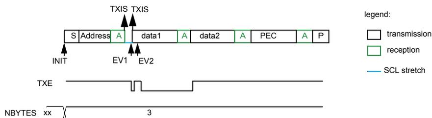
When the IP is used in SMBus, SBC must be programmed to '1' in order to allow the PEC transmission at the end of the programmed number of data bytes. When the PECBYTE bit is set, the number of bytes programmed in NBBYTES[7:0] includes the PEC transmission. In that case the total number of TXIS interrupts is NBBYTES-1 and the content of the I2C_PECR register is automatically transmitted if the controller requests an extra byte after the NBBYTES-1 data transfer.
Caution: The PECBYTE bit has no effect when the RELOAD bit is set.
Figure 117. Transfer sequence flowchart for SMBus target transmitter N bytes + PEC
graph TD
    Start([SMBus target transmission]) --> Init[Target initialization]
    Init --> ADDR{I2C_ISR.ADDR = 1?}
    ADDR -- No --> ADDR
    ADDR -- Yes --> Config[Read ADDCODE and DIR in I2C_ISR
I2C_CR2.NBYTES = N + 1
PECBYTE=1
Set I2C_ICR.ADDRCF]
    Config --> TXIS{I2C_ISR.TXIS = 1?}
    TXIS -- No --> TXIS
    TXIS -- Yes --> Write[Write I2C_TXDR.TXDATA]
    Write --> TXIS
    style ADDR fill:none,stroke:none
    style TXIS fill:none,stroke:none
Figure 118. Transfer bus diagrams for SMBus target transmitter (SBC=1)
Example SMBus target transmitter 2 bytes + PEC,
Legend:
transmission
reception
—
SCL stretch
EV1: ADDR ISR: check ADDCODE, program NBYTES=3, set PECBYTE, set ADDRCF
EV2: TXIS ISR: wr data1
EV3: TXIS ISR: wr data2
SMBus target receiver
When the I 2 C is used in SMBus mode, SBC must be programmed to '1' in order to allow the PEC checking at the end of the programmed number of data bytes. In order to allow the ACK control of each byte, the reload mode must be selected (RELOAD=1).
Refer to Section 21.4.7: I2C target mode "target bite control mode" for more details.
In order to check the PEC byte, the RELOAD bit must be cleared and the PECBYTE bit must be set. In this case, after NBBYTES-1 data have been received, the next received byte is compared with the internal I2C_PECR register content. A NACK is automatically generated if the comparison does not match, and an ACK is automatically generated if the comparison matches, whatever the ACK bit value. Once the PEC byte is received, it is copied into the I2C_RXDR register like any other data, and the RXNE flag is set.
In the case of a PEC mismatch, the PECERR flag is set and an interrupt is generated if the ERRIE bit is set in the I2C_CR1 register.
If no ACK software control is needed, you can program PECBYTE=1 and, in the same write operation, program NBBYTES with the number of bytes to be received in a continuous flow. After NBBYTES-1 are received, the next received byte is checked as being the PEC.
Caution: The PECBYTE bit has no effect when the RELOAD bit is set.
Figure 119. Transfer sequence flowchart for SMBus target receiver N bytes + PEC
graph TD
    Start([SMBus target reception]) --> Init[Target initialization]
    Init --> Addr{I2C_ISR.ADDR = 1?}
    Addr -- No --> Init
    Addr -- Yes --> ReadAddr[Read ADDCODE and DIR in I2C_ISR
I2C_CR2.NBYTES = 1, RELOAD = 1
PECBYTE = 1
Set I2C_ICR.ADDRCF]
    ReadAddr --> Rxne{I2C_ISR.RXNE = 1?
I2C_ISR.TCR = 1?}
    Rxne -- No --> ReadAddr
    Rxne -- Yes --> ReadData1[Read I2C_RXDR.RXDATA
Program I2C_CR2.NACK = 0
I2C_CR2.NBYTES = 1
N = N - 1]
    ReadData1 --> N1{N = 1?}
    N1 -- No --> ReadAddr
    N1 -- Yes --> ReadData2[Read I2C_RXDR.RXDATA
Program RELOAD = 0
NACK = 0 and NBBYTES = 1]
    ReadData2 --> Rxne2{I2C_ISR.RXNE = 1?}
    Rxne2 -- No --> ReadData2
    Rxne2 -- Yes --> ReadData3[Read I2C_RXDR.RXDATA]
    ReadData3 --> End([End])
Figure 120. Bus transfer diagrams for SMBus target receiver (SBC=1)
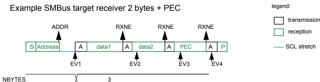
Example SMBus target receiver 2 bytes + PEC
legend:
transmission
reception
— SCL stretch
EV1: ADDR ISR: check ADDCODE and DIR, program NBYTES = 3, PECBYTE=1, RELOAD=0, set ADDRCF
EV2: RXNE ISR: rd data1
EV3: RXNE ISR: rd data2
EV4: RXNE ISR: rd PEC
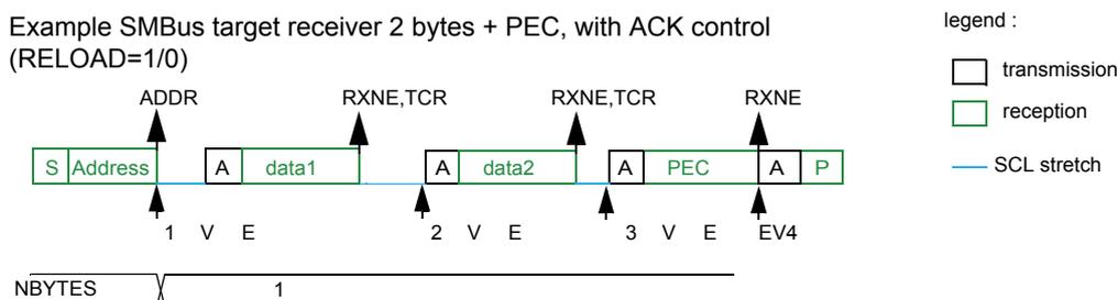
Example SMBus target receiver 2 bytes + PEC, with ACK control (RELOAD=1/0)
legend :
transmission
reception
— SCL stretch
EV1: ADDR ISR: check ADDCODE and DIR, program NBYTES = 1, PECBYTE=1, RELOAD=1, set ADDRCF
EV2: RXNE-TCR ISR: rd data1, program NACK=0 and NBYTES = 1
EV3: RXNE-TCR ISR: rd data2, program NACK=0, NBYTES = 1 and RELOAD=0
EV4: RXNE-TCR ISR: rd PEC
This section is relevant only when SMBus feature is supported. Refer to Section 21.3: I 2 C implementation .
In addition to I 2 C controller transfer management (refer to Section 21.4.8: I2C controller mode ) some additional software flowcharts are provided to support SMBus.
SMBus controller transmitter
When the SMBus controller wants to transmit the PEC, the PECBYTE bit must be set and the number of bytes must be programmed in the NBYTES[7:0] field, before setting the START bit. In this case the total number of TXIS interrupts is NBYTES-1. So if the PECBYTE bit is set when NBYTES=0x1, the content of the I2C_PECR register is automatically transmitted.
If the SMBus controller wants to send a STOP condition after the PEC, automatic end mode should be selected (AUTOEND=1). In this case, the STOP condition automatically follows the PEC transmission.
When the SMBus controller wants to send a RESTART condition after the PEC, software mode must be selected (AUTOEND=0). In this case, once NBYTES-1 have been transmitted, the I2C_PECR register content is transmitted and the TC flag is set after the PEC transmission, stretching the SCL line low. The RESTART condition must be programmed in the TC interrupt subroutine.
Caution: The PECBYTE bit has no effect when the RELOAD bit is set.
Figure 121. Bus transfer diagrams for SMBus controller transmitter
Example SMBus controller transmitter 2 bytes + PEC, automatic end mode (STOP)
INIT: program target address, program NBYTES = 3, AUTOEND=1, set PECBYTE, set START
EV1: TXIS ISR: wr data1
EV2: TXIS ISR: wr data2
Example SMBus controller transmitter 2 bytes + PEC, software end mode (RESTART)
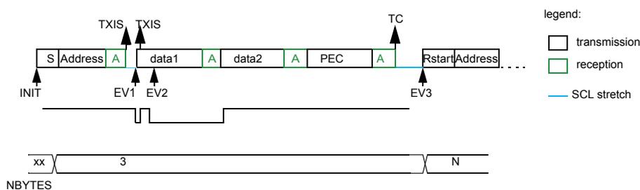
INIT: program target address, program NBYTES = 3, AUTOEND=0, set PECBYTE, set START
EV1: TXIS ISR: wr data1
EV2: TXIS ISR: wr data2
EV3: TC ISR: program target address, program NBYTES = N, set START
SMBus controller receiver
When the SMBus controller wants to receive the PEC followed by a STOP at the end of the transfer, automatic end mode can be selected (AUTOEND=1). The PECBYTE bit must be set and the target address must be programmed, before setting the START bit. In this case, after NBYTES-1 data have been received, the next received byte is automatically checked versus the I2C_PECR register content. A NACK response is given to the PEC byte, followed by a STOP condition.
When the SMBus controller receiver wants to receive the PEC byte followed by a RESTART condition at the end of the transfer, software mode must be selected (AUTOEND=0). The PECBYTE bit must be set and the target address must be programmed, before setting the START bit. In this case, after NBYTES-1 data have been received, the next received byte is automatically checked versus the I2C_PECR register content. The TC flag is set after the PEC byte reception, stretching the SCL line low. The RESTART condition can be programmed in the TC interrupt subroutine.
Caution: The PECBYTE bit has no effect when the RELOAD bit is set.
Figure 122. Bus transfer diagrams for SMBus controller receiver
Example SMBus controller receiver 2 bytes + PEC, automatic end mode (STOP)
The diagram shows a sequence of events: INIT (S, Address, A), data1 (RXNE), data2 (RXNE), PEC (RXNE), NA, and P. The NBYTES register is set to 3. The legend indicates transmission (white), reception (green), and SCL stretch (blue line).
INIT: program target address, program NBYTES = 3, AUTOEND=1, set PECBYTE, set START
EV1: RXNE ISR: rd data1
EV2: RXNE ISR: rd data2
EV3: RXNE ISR: rd PEC
Example SMBus controller receiver 2 bytes + PEC, software end mode (RESTART)
The diagram shows a sequence of events: INIT (S, Address, A), data1 (RXNE), data2 (RXNE), PEC (RXNE), NA (TC), and Restart Address. The NBYTES register is set to 3. The legend indicates transmission (white), reception (green), and SCL stretch (blue line).
INIT: program target address, program NBYTES = 3, AUTOEND=0, set PECBYTE, set START
EV1: RXNE ISR: rd data1
EV2: RXNE ISR: rd data2
EV3: RXNE ISR: read PEC
EV4: TC ISR: program target address, program NBYTES = N, set START
21.4.14 Error conditions
The following are error conditions which may cause communication to fail.
Bus error (BERR)
A bus error is detected when a START or a STOP condition is detected and is not located after a multiple of 9 SCL clock pulses. A START or a STOP condition is detected when an SDA edge occurs while SCL is high.
The bus error flag is set only if the I 2 C is involved in the transfer as controller or addressed target (i.e not during the address phase in target mode).
In case of a misplaced START or RESTART detection in target mode, the I 2 C enters address recognition state like for a correct START condition.
When a bus error is detected, the BERR flag is set in the I2C_ISR register, and an interrupt is generated if the ERRIE bit is set in the I2C_CR1 register.
Arbitration loss (ARLO)
An arbitration loss is detected when a high level is sent on the SDA line, but a low level is sampled on the SCL rising edge.
- • In controller mode, arbitration loss is detected during the address phase, data phase and data acknowledge phase. In this case, the SDA and SCL lines are released, the START control bit is cleared by hardware and the controller switches automatically to target mode.
- • In target mode, arbitration loss is detected during data phase and data acknowledge phase. In this case, the transfer is stopped, and the SCL and SDA lines are released.
When an arbitration loss is detected, the ARLO flag is set in the I2C_ISR register, and an interrupt is generated if the ERRIE bit is set in the I2C_CR1 register.
Overrun/underrun error (OVR)
An overrun or underrun error is detected in target mode when NOSTRETCH=1 and:
- • In reception when a new byte is received and the RXDR register has not been read yet. The new received byte is lost, and a NACK is automatically sent as a response to the new byte.
- • In transmission:
- – When STOPF=1 and the first data byte should be sent. The content of the I2C_TXDR register is sent if TXE=0, 0xFF if not.
- – When a new byte should be sent and the I2C_TXDR register has not been written yet, 0xFF is sent.
When an overrun or underrun error is detected, the OVR flag is set in the I2C_ISR register, and an interrupt is generated if the ERRIE bit is set in the I2C_CR1 register.
Packet Error Checking Error (PECERR)
This section is relevant only when the SMBus feature is supported. Refer to Section 21.3: I 2 C implementation .
A PEC error is detected when the received PEC byte does not match with the I2C_PECR register content. A NACK is automatically sent after the wrong PEC reception.
When a PEC error is detected, the PECERR flag is set in the I2C_ISR register, and an interrupt is generated if the ERRIE bit is set in the I2C_CR1 register.
Timeout Error (TIMEOUT)
This section is relevant only when the SMBus feature is supported. Refer to Section 21.3: I 2 C implementation .
A timeout error occurs for any of these conditions:
- • TIDLE=0 and SCL remained low for the time defined in the TIMEOUTA[11:0] bits: this is used to detect a SMBus timeout
- • TIDLE=1 and both SDA and SCL remained high for the time defined in the TIMEOUTA [11:0] bits: this is used to detect a bus idle condition
- • Controller cumulative clock low extend time reached the time defined in the TIMEOUTB[11:0] bits (SMBus tLOW:MEXTparameter)
- • Target cumulative clock low extend time reached the time defined in TIMEOUTB[11:0] bits (SMBus tLOW:SEXTparameter).
When a timeout violation is detected in controller mode, a STOP condition is automatically sent.
When a timeout violation is detected in target mode, SDA and SCL lines are automatically released.
When a timeout error is detected, the TIMEOUT flag is set in the I2C_ISR register, and an interrupt is generated if the ERRIE bit is set in the I2C_CR1 register.
Alert (ALERT)
This section is relevant only when the SMBus feature is supported. Refer to Section 21.3: I 2 C implementation .
The ALERT flag is set when the I 2 C interface is configured as a host (SMBHEN=1), the alert pin detection is enabled (ALERTEN=1) and a falling edge is detected on the SMBA pin. An interrupt is generated if the ERRIE bit is set in the I2C_CR1 register.
21.4.15 DMA requests
Transmission using DMA
DMA (Direct Memory Access) can be enabled for transmission by setting the TXDMAEN bit in the I2C_CR1 register. Data is loaded from an SRAM area configured using the DMA peripheral (see DMA controller (DMA)) to the I2C_TXDR register whenever the TXIS bit is set.
Only the data are transferred with DMA.
- • In controller mode: the initialization, the target address, direction, number of bytes and START bit are programmed by software (the transmitted target address cannot be transferred with DMA). When all data are transferred using DMA, the DMA must be initialized before setting the START bit. The end of transfer is managed with the NBYPES counter.
- • In target mode:
- – With NOSTRETCH=0, when all data are transferred using DMA, the DMA must be initialized before the address match event, or in ADDR interrupt subroutine, before clearing ADDR
- – With NOSTRETCH=1, the DMA must be initialized before the address match event.
- • For instances supporting SMBus: the PEC transfer is managed with NBYPES counter.
Refer to Section 21.4.13: SMBus target mode "SMBus target transmitter" and "SMBus controller transmitter" for more details.
Note: If DMA is used for transmission, the TXIE bit does not need to be enabled.
Reception using DMA
DMA (direct memory access) can be enabled for reception by setting the RXDMAEN bit in the I2C_CR1 register. Data is loaded from the I2C_RXDR register to an SRAM area configured using the DMA peripheral (refer to DMA controller (DMA)) whenever the RXNE bit is set. Only the data (including PEC) are transferred with DMA.
- • In controller mode, the initialization, the target address, direction, number of bytes and START bit are programmed by software. When all data are transferred using DMA, the DMA must be initialized before setting the START bit. The end of transfer is managed with the NBYTES counter.
- • In target mode with NOSTRETCH=0, when all data are transferred using DMA, the DMA must be initialized before the address match event, or in the ADDR interrupt subroutine, before clearing the ADDR flag.
- • If SMBus is supported (see Section 21.3: I 2 C implementation ): the PEC transfer is managed with the NBYTES counter.
Note: If DMA is used for reception, the RXIE bit does not need to be enabled.
21.5 I2C interrupts
The table below gives the list of I 2 C interrupt requests.
Table 95. I 2 C interrupt requests
| Interrupt event | Event flag | Event flag/interrupt clearing method | Interrupt enable control bit |
|---|---|---|---|
| Receive buffer not empty | RXNE | Read I2C_RXDR register | RXIE |
| Transmit buffer interrupt status | TXIS | Write I2C_TXDR register | TXIE |
| Stop detection interrupt flag | STOPF | Write STOPCF=1 | STOPIE |
| Transfer complete reload | TCR | Write I2C_CR2 with NBYTES[7:0] 1 0 | TCIE |
| Transfer complete | TC | Write START=1 or STOP=1 | |
| Address matched | ADDR | Write ADDRCF=1 | ADDRIE |
| NACK reception | NACKF | Write NACKCF=1 | NACKIE |
| Bus error | BERR | Write BERRCF=1 | ERRIE |
| Arbitration loss | ARLO | Write ARLOCF=1 | |
| Overrun/underrun | OVR | Write OVRCF=1 | |
| PEC error | PECERR | Write PECERRCF=1 | |
| Timeout/t LOW error | TIMEOUT | Write TIMEOUTCF=1 | |
| SMBus alert | ALERT | Write ALERTCF=1 |
Depending on the product implementation, all these interrupt events can either share the same interrupt vector (I 2 C global interrupt), or be grouped into 2 interrupt vectors ( I 2 C event interrupt and I 2 C error interrupt, see Section 2.3.2: Interrupts ). In order to enable the I 2 C interrupts, the following sequence is required:
- • Configure and enable the I 2 C IRQ channel in the NVIC
- • Configure the I 2 C to generate interrupts
Figure 123. I 2 C interrupt mapping diagram
The diagram illustrates the logic for generating I 2 C interrupts based on various status flags. It is divided into three main sections:
- I2C event interrupt:
This interrupt is generated by an OR gate that combines the outputs of several AND gates. The inputs to these AND gates are:
- TCR and TC (outputting to an OR gate, then an AND gate with TCIE)
- TXIS and TXIE (outputting to an AND gate)
- RXNE and RXE (outputting to an AND gate)
- STOPF and STOPIE (outputting to an AND gate)
- ADDR and ADDRIE (outputting to an AND gate)
- NACKF and NACKIE (outputting to an AND gate)
- I2C error interrupt:
This interrupt is generated by an AND gate that combines the output of a large OR gate with the ERRIE flag. The inputs to the large OR gate are:
- BERR
- OVR
- ARLO
- TIMEOUT
- ALERT
- PECERR
- I2C global interrupt: This is the final output, generated by an OR gate that combines the "I2C event interrupt" and the "I2C error interrupt" signals.
21.6 I2C registers
Refer to Section 1.5: Acronyms for a list of abbreviations used in register descriptions. The peripheral registers are accessed by words (32-bit).
21.6.1 Control register 1 (I2C_CR1)
Address offset: 0x00 Reset value: 0x0000 0000
Access: no wait states, except if a write access occurs while a write access to this register is on-going. In this case, wait states are inserted in the second write access until the previous one is completed. The latency of the second write access can be up to \( 2 \times PCLK1 + 6 \times I2CCLK \) .
| 31 | 30 | 29 | 28 | 27 | 26 | 25 | 24 | 23 | 22 | 21 | 20 | 19 | 18 | 17 | 16 |
|---|---|---|---|---|---|---|---|---|---|---|---|---|---|---|---|
| Res. | Res. | Res. | Res. | Res. | Res. | Res. | Res. | PECEN | ALERT EN | SMBD EN | SMBH EN | GCEN | Res. | NOSTR ETCH | SBC |
| rw | rw | rw | rw | rw | rw | rw | |||||||||
| 15 | 14 | 13 | 12 | 11 | 10 | 9 | 8 | 7 | 6 | 5 | 4 | 3 | 2 | 1 | 0 |
| RXDMA EN | TXDMA EN | Res. | ANF OFF | DNF | ERRIE | TCIE | STOP IE | NACK IE | ADDR IE | RXIE | TXIE | PE | |||
| rw | rw | rw | rw | rw | rw | rw | rw | rw | rw | rw | rw | ||||
| Bits 31:24 | Reserved, must be kept at reset value. |
| Bit 23 | PECEN: PEC enable. 0: PEC calculation disabled Note: If the SMBus feature is not supported, this bit is reserved and forced by hardware to '0'. Refer to Section 21.3: I 2 C implementation . |
| Bit 22 | ALERTEN: SMBus alert enable. Device mode (SMBHEN=0): 0: Releases SMBA pin high and alert response Address Header disabled: 0001100x followed by NACK Host mode (SMBHEN=1): 0: SMBus alert pin (SMBA) not supported Note: When ALERTEN=0, the SMBA pin can be used as a standard GPIO. If the SMBus feature is not supported, this bit is reserved and forced by hardware to '0'. Refer to Section 21.3: I 2 C implementation . |
| Bit 21 | SMBDEN: SMBus Device Default address enable. 0: Device default address disabled. Address 0b1100001x is NACKed. Note: If the SMBus feature is not supported, this bit is reserved and forced by hardware to '0'. Refer to Section 21.3: I 2 C implementation . |
| Bit 20 | SMBHEN: SMBus Host address enable. 0: Host address disabled. Address 0b0001000x is NACKed. Note: If the SMBus feature is not supported, this bit is reserved and forced by hardware to '0'. Refer to Section 21.3: I 2 C implementation . |
| Bit 19 | GCEN: General call enable. 0: General call disabled. Address 0b00000000 is NACKed. |
| 1: General call enabled. Address 0b00000000 is ACKed. | |
| Bit 18 | Reserved, must be kept at reset value. |
| Bit 17 | NOSTRETCH:
Clock stretching disable. This bit is used to disable clock stretching in target mode. It must be kept cleared in controller mode. 0: Clock stretching enabled 1: Clock stretching disabled Note: This bit can only be programmed when the I 2 C is disabled (PE = 0). |
| Bit 16 | SBC:
Target byte control. This bit is used to enable hardware byte control in target mode. 0: Target byte control disabled 1: Target byte control enabled |
| Bit 15 | RXDMAEN:
DMA reception requests enable 0: DMA mode disabled for reception 1: DMA mode enabled for reception |
| Bit 14 | TXDMAEN:
DMA transmission requests enable. 0: DMA mode disabled for transmission 1: DMA mode enabled for transmission |
| Bit 13 | Reserved, must be kept at reset value. |
| Bit 12 | ANFOFF:
Analog noise filter OFF. 0: Analog noise filter enabled 1: Analog noise filter disabled Note: This bit can only be programmed when the I 2 C is disabled (PE = 0). |
| Bits 11:8 | DNF[3:0]:
Digital noise filter. These bits are used to configure the digital noise filter on SDA and SCL input. The digital filter filters spikes with a length of up to DNF[3:0] * t I2CCLK . 0000: Digital filter disabled 0001: Digital filter enabled and filtering capability up to 1 t I2CCLK ... 1111: Digital filter enabled and filtering capability up to 15 t I2CCLK Note: If the analog filter is also enabled, the digital filter is added to the analog filter. This filter can only be programmed when the I 2 C is disabled (PE = 0). |
| Bit 7 | ERRIE:
Error interrupts enable. 0: Error detection interrupts disabled 1: Error detection interrupts enabled Note: Any of these errors generate an interrupt: Arbitration Loss (ARLO). Bus Error detection (BERR) Overrun/Underrun (OVR) Timeout detection (TIMEOUT) PEC error detection (PECERR) Alert pin event detection (ALERT) |
| Bit 6 | TCIE:
Transfer complete interruptenable. 0: Transfer complete interrupt disabled 1: Transfer complete interrupt enabled Note: Any of these events generate an interrupt: |
| 0: transfer complete (TC) 1: transfer complete reload (TCR). | |
| Bit 5 | STOPIE
: STOP detection Interrupt enable. 0: Stop detection (STOPF) interrupt disabled 1: Stop detection (STOPF) interrupt enabled |
| Bit 4 | NACKIE
: Not acknowledge received interrupt enable. 0: Not acknowledge (NACKF) received interrupts disabled 1: Not acknowledge (NACKF) received interrupts enabled |
| Bit 3 | ADDRIE
: Address match interrupt enable (target only). 0: Address match (ADDR) interrupts disabled 1: Address match (ADDR) interrupts enabled |
| Bit 2 | RXIE
: RX Interrupt enable. 0: Receive (RXNE) interrupt disabled 1: Receive (RXNE) interrupt enabled |
| Bit 1 | TXIE
: TX interrupt enable. 0: Transmit (TXIS) interrupt disabled 1: Transmit (TXIS) interrupt enabled |
| Bit 0 | PE
: Peripheral enable. 0: Peripheral disable 1: Peripheral enable Note: When PE=0, the I 2 C SCL and SDA lines are released. Internal state machines and status bits are put back to their reset value. When cleared, PE must be kept low for at least 3 APB clock cycles. |
21.6.2 Control register 2 (I2C_CR2)
Address offset: 0x04
Reset value: 0x0000 0000
Access: no wait states, except if a write access occurs while a write access to this register is on-going. In this case, wait states are inserted in the second write access until the previous one is completed. The latency of the second write access can be up to \( 2 \times PCLK1 + 6 \times I2CCLK \) .
| 31 | 30 | 29 | 28 | 27 | 26 | 25 | 24 | 23 | 22 | 21 | 20 | 19 | 18 | 17 | 16 |
| Res. | Res. | Res. | Res. | Res. | PEC BYTE | AUTO END | RE LOAD | NBBYTES[7:0] | |||||||
| rs | rw | rw | rw | ||||||||||||
| 15 | 14 | 13 | 12 | 11 | 10 | 9 | 8 | 7 | 6 | 5 | 4 | 3 | 2 | 1 | 0 |
| NACK | STOP | START | HEAD 10R | ADD10 | RD_W RN | SADD[9:0] | |||||||||
| rs | rs | rs | rw | rw | rw | rw | |||||||||
| Bits 31:27 | Reserved, must be kept at reset value. |
| Bit 26 | PECBYTE : Packet error checking byte. This bit is set by software, and cleared by hardware when the PEC is transferred, or when a STOP condition or an Address matched is received, also when PE=0. 0: No PEC transfer 1: PEC transmission/reception is requested Note: Writing '0' to this bit has no effect. This bit has no effect when RELOAD is set. This bit has no effect in target mode when SBC=0. If the SMBus feature is not supported, this bit is reserved and forced by hardware to '0'. Refer to Section 21.3: I 2 C implementation . |
| Bit 25 | AUTOEND : Automatic end mode (controller mode). This bit is set and cleared by software. 0: Software end mode: TC flag is set when NBBYTES data are transferred, stretching SCL low. 1: Automatic end mode: a STOP condition is automatically sent when NBBYTES data are transferred. Note: This bit has no effect in target mode or when the RELOAD bit is set. |
| Bit 24 | RELOAD : NBBYTES reload mode. This bit is set and cleared by software. 0: The transfer is completed after the NBBYTES data transfer (STOP or RESTART follows) 1: The transfer is not completed after the NBBYTES data transfer (NBBYTES is reloaded). TCR flag is set when NBBYTES data are transferred, stretching SCL low. |
| Bits 23:16 | NBYTES[7:0] : Number of bytes. The number of bytes to be transmitted/received is programmed there. This field have no effect in target mode with SBC=0. Note: Changing these bits when the START bit is set is not allowed. |
| Bit 15 | NACK : NACK generation (target mode). The bit is set by software, cleared by hardware when the NACK is sent, or when a STOP condition or an Address matched is received, or when PE=0. 0: An ACK is sent after current received byte. 1: A NACK is sent after current received byte. Note: Writing '0' to this bit has no effect. This bit is used in target mode only: in controller receiver mode, NACK is automatically generated after last byte preceding STOP or RESTART condition, whatever the NACK bit value. When an overrun occurs in target receiver NOSTRETCH mode, a NACK is automatically generated whatever the NACK bit value. |
| When hardware PEC checking is enabled (PECBYTE=1), the PEC acknowledge value does not depend on the NACK value. | |
| Bit 14 | STOP: Stop generation (controller mode). The bit is set by software, cleared by hardware when a Stop condition is detected, or when PE=0. In controller Mode: 0: No stop generation 1: Stop generation after current byte transfer Note: Writing '0' to this bit has no effect. |
| Bit 13 | START: Start generation. This bit is set by software, and cleared by hardware after the Start followed by the address sequence is sent, by an arbitration loss, by a timeout error detection, or when PE = 0. It can also be cleared by software by writing '1' to the ADDRCF bit in the I2C_ICR register. 0: No start generation 1: Restart/start generation:
Note: Writing '0' to this bit has no effect. The START bit can be set even if the bus is BUSY or I 2 C is in target mode. This bit has no effect when RELOAD is set. |
| Bit 12 | HEAD10R: 10-bit address header only read direction (controller receiver mode). 0: The controller sends the complete 10 bit target address read sequence: start + 2 bytes 10-bit address in write direction + restart + 1 st 7 bits of the 10-bit address in read direction 1: The controller only sends the 1 st 7 bits of the 10-bit address, followed by Read direction Note: Changing this bit when the START bit is set is not allowed. |
| Bit 11 | ADD10: 10-bit addressing mode (controller mode). 0: The controller operates in 7-bit addressing mode 1: The controller operates in 10-bit addressing mode Note: Changing this bit when the START bit is set is not allowed. |
| Bit 10 | RD_WRN: Transfer direction (controller mode). 0: Controller requests a write transfer 1: Controller requests a read transfer Note: Changing this bit when the START bit is set is not allowed. |
| Bits 9:8 | SADD[9:8]: Target address bit 9:8 (controller mode). In 7-bit addressing mode (ADD10 = 0): These bits have no effect. In 10-bit addressing mode (ADD10 = 1): These bits should be written with bits 9:8 of the target address to be sent Note: Changing these bits when the START bit is set is not allowed. |
| Bits 7:1 | SADD[7:1]: Target address bit 7:1 (controller mode). In 7-bit addressing mode (ADD10 = 0): These bits should be written with the 7-bit target address to be sent In 10-bit addressing mode (ADD10 = 1): These bits should be written with bits 7:1 of the target address to be sent Note: Changing these bits when the START bit is set is not allowed. |
| Bit 0 | SADD0: Target address bit 0 (controller mode). In 7-bit addressing mode (ADD10 = 0): This bit is do not care In 10-bit addressing mode (ADD10 = 1): This bit should be written with bit 0 of the target address to be sent |
| Note: Changing these bits when the START bit is set is not allowed. |
21.6.3 Own address 1 register (I2C_OAR1)
Address offset: 0x08
Reset value: 0x0000 0000
Access: no wait states, except if a write access occurs while a write access to this register is on-going. In this case, wait states are inserted in the second write access until the previous one is completed. The latency of the second write access can be up to \( 2 \times PCLK1 + 6 \times I2CCLK \) .
| 31 | 30 | 29 | 28 | 27 | 26 | 25 | 24 | 23 | 22 | 21 | 20 | 19 | 18 | 17 | 16 |
| Res. | Res. | Res. | Res. | Res. | Res. | Res. | Res. | Res. | Res. | Res. | Res. | Res. | Res. | Res. | Res. |
| 15 | 14 | 13 | 12 | 11 | 10 | 9 | 8 | 7 | 6 | 5 | 4 | 3 | 2 | 1 | 0 |
| OA1EN | Res. | Res. | Res. | Res. | OA1 MODE | OA1[9:8] | OA1[7:1] | OA1[0] | |||||||
| r/w | r/w | r/w | r/w | r/w | |||||||||||
| Bits 31:16 | Reserved, must be kept at reset value. |
| Bit 15 | OA1EN:
Own address 1 enable. 0: Own address 1 disabled. The received target address OA1 is NACKed. 1: Own address 1 enabled. The received target address OA1 is ACKed. |
| Bits 14:11 | Reserved, must be kept at reset value. |
| Bit 10 | OA1MODE
Own address 1 10-bit mode. 0: Own address 1 is a 7-bit address 1: Own address 1 is a 10-bit address Note: This bit can be written only when OA1EN=0. |
| Bits 9:8 | OA1[9:8]:
Interface address. 7-bit addressing mode: do not care 10-bit addressing mode: bits 9:8 of address Note: These bits can be written only when OA1EN=0. |
| Bits 7:1 | OA1[7:1]:
Interface address bits 7:1 of address. Note: These bits can be written only when OA1EN=0. |
| Bit 0 | OA1[0]:
Interface address. 7-bit addressing mode: do not care 10-bit addressing mode: bit 0 of address Note: This bit can be written only when OA1EN=0. |
21.6.4 Own address 2 register (I2C_OAR2)
Address offset: 0x0C
Reset value: 0x0000 0000
Access: no wait states, except if a write access occurs while a write access to this register is on-going. In this case, wait states are inserted in the second write access until the previous one is completed. The latency of the second write access can be up to \( 2 \times PCLK1 + 6 \times I2CCLK \) .
| 31 | 30 | 29 | 28 | 27 | 26 | 25 | 24 | 23 | 22 | 21 | 20 | 19 | 18 | 17 | 16 |
| Res. | Res. | Res. | Res. | Res. | Res. | Res. | Res. | Res. | Res. | Res. | Res. | Res. | Res. | Res. | Res. |
| 15 | 14 | 13 | 12 | 11 | 10 | 9 | 8 | 7 | 6 | 5 | 4 | 3 | 2 | 1 | 0 |
| OA2EN | Res. | Res. | Res. | Res. | OA2MSK[2:0] | OA2[7:1] | Res. | ||||||||
| rw | rw | rw | |||||||||||||
| Bits 31:16 | Reserved, must be kept at reset value. |
| Bit 15 | OA2EN:
Own address 2 enable. 0: Own address 2 disabled. The received target address OA2 is NACKed. 1: Own address 2 enabled. The received target address OA2 is ACKed. |
| Bits 14:11 | Reserved, must be kept at reset value. |
| Bits 10:8 | OA2MSK[2:0]:
Own Address 2 masks. 000: No mask 001: OA2[1] is masked and has no effect. Only OA2[7:2] are compared. 010: OA2[2:1] are masked and has no effect. Only OA2[7:3] are compared. 011: OA2[3:1] are masked and has no effect. Only OA2[7:4] are compared. 100: OA2[4:1] are masked and has no effect. Only OA2[7:5] are compared. 101: OA2[5:1] are masked and has no effect. Only OA2[7:6] are compared. 110: OA2[6:1] are masked and has no effect. Only OA2[7] is compared. 111: OA2[7:1] are masked and has no effect. No comparison is done, and all (except reserved) 7-bit received addresses are acknowledged. Note: These bits can be written only when OA2EN=0. As soon as OA2MSK is not equal to 0, the reserved I 2 C addresses (0b0000xxx and 0b1111xxx) are not acknowledged even if the comparison matches. |
| Bits 7:1 | OA2[7:1]:
Interface address bits 7:1 of address. Note: These bits can be written only when OA2EN=0. |
| Bit 0 | Reserved, must be kept at reset value. |
21.6.5 Timing register (I2C_TIMINGR)
Address offset: 0x10
Reset value: 0x0000 0000
Access: no wait states
| 31 | 30 | 29 | 28 | 27 | 26 | 25 | 24 | 23 | 22 | 21 | 20 | 19 | 18 | 17 | 16 |
| PRESC[3:0] | Res. | Res. | Res. | Res. | SCLDEL[3:0] | SDADEL[3:0] | |||||||||
| rw | rw | rw | |||||||||||||
| 15 | 14 | 13 | 12 | 11 | 10 | 9 | 8 | 7 | 6 | 5 | 4 | 3 | 2 | 1 | 0 |
| SCLH[7:0] | SCLL[7:0] | ||||||||||||||
| rw | rw | ||||||||||||||
| Bits 31:28 | PRESC[3:0]: Timing prescaler. This field is used to prescale I2CCLK in order to generate the clock period \( t_{\text{PRESC}} \) used for data setup and hold counters and for SCL high and low level counters. \[
t_{\text{PRESC}} = (\text{PRESC}+1) \times t_{\text{I2CCLK}}
\] |
| Bits 27:24 | Reserved, must be kept at reset value. |
| Bits 23:20 | SCLDEL[3:0]: Data setup time. This field is used to generate a delay \( t_{\text{SCLDEL}} \) between SDA edge and SCL rising edge in transmission mode. \[
t_{\text{SCLDEL}} = (\text{SCLDEL}+1) \times t_{\text{PRESC}}
\] Note: \( t_{\text{SCLDEL}} \) is used to generate \( t_{\text{SU:DAT}} \) timing. |
| Bits 19:16 | SDADEL[3:0]: Data hold time. This field is used to generate the delay \( t_{\text{SDADEL}} \) between SCL falling edge SDA edge in transmission mode. \[
t_{\text{SDADEL}} = \text{SDADEL} \times t_{\text{PRESC}}
\] Note: SDADEL is used to generate \( t_{\text{HD:DAT}} \) timing. |
| Bits 15:8 | SCLH[7:0]: SCL high period (controller mode). This field is used to generate the SCL high period in controller mode. \( t_{\text{SCLH}} = (\text{SCLH}+1) \times t_{\text{PRESC}} \) . Note: SCLH is also used to generate \( t_{\text{SU:STA}} \) and \( t_{\text{HD:STA}} \) timing. |
| Bits 7:0 | SCLL[7:0]: SCL low period (controller mode). This field is used to generate the SCL low period in controller mode. \( t_{\text{SCLL}} = (\text{SCLL}+1) \times t_{\text{PRESC}} \) . Note: SCLL is also used to generate \( t_{\text{BUF}} \) and \( t_{\text{SU:STA}} \) timings. |
Note: This register must be configured when the I 2 C is disabled (PE = 0).
21.6.6 Timeout register (I2C_TIMEOUTR)
Address offset: 0x14
Reset value: 0x0000 0000
Access: no wait states, except if a write access occurs while a write access to this register is on-going. In this case, wait states are inserted in the second write access until the previous one is completed. The latency of the second write access can be up to \( 2 \times PCLK1 + 6 \times I2CCLK \) .
| 31 | 30 | 29 | 28 | 27 | 26 | 25 | 24 | 23 | 22 | 21 | 20 | 19 | 18 | 17 | 16 |
| TEXTEN | Res. | Res. | Res. | TIMEOUTB [11:0] | |||||||||||
| rw | rw | ||||||||||||||
| 15 | 14 | 13 | 12 | 11 | 10 | 9 | 8 | 7 | 6 | 5 | 4 | 3 | 2 | 1 | 0 |
| TIMOUTEN | Res. | Res. | TIDLE | TIMEOUTA [11:0] | |||||||||||
| rw | rw | rw | |||||||||||||
| Bit 31 | TEXTEN:
Extended clock timeout enable. 0: Extended clock timeout detection is disabled 1: Extended clock timeout detection is enabled. When a cumulative SCL stretch for more than \( t_{LOW:EXT} \) is done by the I 2 C interface, a timeout error is detected (TIMEOUT=1). |
| Bits 30:28 | Reserved, must be kept at reset value. |
| Bits 27:16 | TIMEOUTB[11:0]:
Bus timeout B. This field is used to configure the cumulative clock extension timeout: In controller mode, the controller cumulative clock low extend time ( \( t_{LOW:MEXT} \) ) is detected in target mode, the target cumulative clock low extend time ( \( t_{LOW:SEXT} \) ) is detected \( t_{LOW:EXT} = (TIMEOUTB+1) \times 2048 \times t_{I2CCLK} \) . Note: These bits can be written only when TEXTEN=0. |
| Bit 15 | TIMOUTEN:
Clock timeout enable. 0: SCL timeout detection is disabled 1: SCL timeout detection is enabled: when SCL is low for more than \( t_{TIMEOUT} \) (TIDLE=0) or high for more than \( t_{IDLE} \) (TIDLE=1), a timeout error is detected (TIMEOUT=1) |
| Bits 14:13 | Reserved, must be kept at reset value. |
| Bit 12 | TIDLE:
Idle clock timeout detection. 0: TIMEOUTA is used to detect SCL low timeout 1: TIMEOUTA is used to detect both SCL and SDA high timeout (bus idle condition) Note: This bit can be written only when TIMOUTEN=0. |
| Bits 11:0 | TIMEOUTA[11:0]:
Bus timeout A. This field is used to configure:
|
Note: If the SMBus feature is not supported, this register is reserved and forced by hardware to "0x00000000". Refer to Section 21.3: I 2 C implementation.
21.6.7 Interrupt and status register (I2C_ISR)
Address offset: 0x18
Reset value: 0x0000 0001
Access: no wait states
| 31 | 30 | 29 | 28 | 27 | 26 | 25 | 24 | 23 | 22 | 21 | 20 | 19 | 18 | 17 | 16 |
|---|---|---|---|---|---|---|---|---|---|---|---|---|---|---|---|
| Res. | Res. | Res. | Res. | Res. | Res. | Res. | Res. | ADDCODE[6:0] | DIR | ||||||
| r | r | ||||||||||||||
| 15 | 14 | 13 | 12 | 11 | 10 | 9 | 8 | 7 | 6 | 5 | 4 | 3 | 2 | 1 | 0 |
| BUSY | Res. | ALERT | TIME OUT | PEC ERR | OVR | ARLO | BERR | TCR | TC | STOPF | NACKF | ADDR | RXNE | TXIS | TXE |
| r | r | r | r | r | r | r | r | r | r | r | r | r | rs | rs | |
| Bits 31:24 | Reserved, must be kept at reset value. |
| Bits 23:17 | ADDCODE[6:0]:
Address match code (target mode). These bits are updated with the received address when an address match event occurs (ADDR = 1). In the case of a 10-bit address, ADDCODE provides the 10-bit header followed by the 2 MSBs of the address. |
| Bit 16 | DIR:
Transfer direction (target mode). This flag is updated when an address match event occurs (ADDR=1). 0: Write transfer, target enters receiver mode 1: Read transfer, target enters transmitter mode |
| Bit 15 | BUSY:
Bus busy. This flag indicates that a communication is in progress on the bus. It is set by hardware when a START condition is detected. It is cleared by hardware when a stop condition is detected, or when PE=0. |
| Bit 14 | Reserved, must be kept at reset value. |
| Bit 13 | ALERT:
SMBus alert. This flag is set by hardware when SMBHEN=1 (SMBus host configuration), ALERTEN=1 and an SMBALERT event (falling edge) is detected on SMBA pin. It is cleared by software by setting the ALERTCF bit. Note: This bit is cleared by hardware when PE=0. If the SMBus feature is not supported, this bit is reserved and forced by hardware to '0'. Refer to Section 21.3: I 2 C implementation . |
| Bit 12 | TIMEOUT:
Timeout or t
LOW
detection flag. This flag is set by hardware when a timeout or extended clock timeout occurred. It is cleared by software by setting the TIMEOUTCF bit. Note: This bit is cleared by hardware when PE=0. If the SMBus feature is not supported, this bit is reserved and forced by hardware to '0'. Refer to Section 21.3: I 2 C implementation . |
| Bit 11 | PECERR:
PEC error in reception. This flag is set by hardware when the received PEC does not match with the PEC register content. A NACK is automatically sent after the wrong PEC reception. It is cleared by software by setting the PECCF bit. Note: This bit is cleared by hardware when PE=0. If the SMBus feature is not supported, this bit is reserved and forced by hardware to '0'. Refer to Section 21.3: I 2 C implementation . |
| Bit 10 | OVR:
Overrun/underrun (target mode). This flag is set by hardware in target mode with NOSTRETCH=1, when an overrun/underrun error occurs. It is cleared by software by setting the OVRCF bit. Note: This bit is cleared by hardware when PE=0. |
| Bit 9 | ARLO: Arbitration loss. This flag is set by hardware in case of arbitration loss. It is cleared by software by setting the ARLOCF bit. Note: This bit is cleared by hardware when PE=0. |
| Bit 8 | BERR: Bus error. This flag is set by hardware when a misplaced Start or Stop condition is detected whereas the peripheral is involved in the transfer. The flag is not set during the address phase in target mode. It is cleared by software by setting BERRCF bit. Note: This bit is cleared by hardware when PE=0. |
| Bit 7 | TCR: Transfer complete reload. This flag is set by hardware when RELOAD=1 and NBYTES data have been transferred. It is cleared by software when NBYTES is written to a non-zero value. Note: This bit is cleared by hardware when PE=0. This flag is only for controller mode, or for target mode when the SBC bit is set. |
| Bit 6 | TC: Transfer complete (controller mode). This flag is set by hardware when RELOAD=0, AUTOEND=0 and NBYTES data have been transferred. It is cleared by software when START bit or STOP bit is set. Note: This bit is cleared by hardware when PE=0. |
| Bit 5 | STOPF: Stop detection flag. This flag is set by hardware when a stop condition is detected on the bus and the peripheral is involved in this transfer:
It is cleared by software by setting the STOPCF bit. Note: This bit is cleared by hardware when PE=0. |
| Bit 4 | NACKF: Not acknowledge received flag. This flag is set by hardware when a NACK is received after a byte transmission. It is cleared by software by setting the NACKCF bit. Note: This bit is cleared by hardware when PE=0. |
| Bit 3 | ADDR: Address matched (target mode). This bit is set by hardware as soon as the received target address matched with one of the enabled target addresses. It is cleared by software by setting ADDRCF bit. Note: This bit is cleared by hardware when PE=0. |
| Bit 2 | RXNE: Receive data register not empty (receivers). This bit is set by hardware when the received data is copied into the I2C_RXDR register, and is ready to be read. It is cleared when I2C_RXDR is read. Note: This bit is cleared by hardware when PE=0. |
| Bit 1 | TXIS: Transmit interrupt status (transmitters). This bit is set by hardware when the I2C_TXDR register is empty and the data to be transmitted must be written in the I2C_TXDR register. It is cleared when the next data to be sent is written in the I2C_TXDR register. This bit can be written to '1' by software when NOSTRETCH=1 only, in order to generate a TXIS event (interrupt if TXIE=1 or DMA request if TXDMAEN=1). Note: This bit is cleared by hardware when PE=0. |
| Bit 0 | TXE: Transmit data register empty (transmitters). This bit is set by hardware when the I2C_TXDR register is empty. It is cleared when the next data to be sent is written in the I2C_TXDR register. This bit can be written to '1' by software in order to flush the transmit data register I2C_TXDR. Note: This bit is set by hardware when PE=0. |
21.6.8 Interrupt clear register (I2C_ICR)
Address offset: 0x1C
Reset value: 0x0000 0000
Access: no wait states
| 31 | 30 | 29 | 28 | 27 | 26 | 25 | 24 | 23 | 22 | 21 | 20 | 19 | 18 | 17 | 16 |
|---|---|---|---|---|---|---|---|---|---|---|---|---|---|---|---|
| Res. | Res. | Res. | Res. | Res. | Res. | Res. | Res. | Res. | Res. | Res. | Res. | Res. | Res. | Res. | Res. |
| 15 | 14 | 13 | 12 | 11 | 10 | 9 | 8 | 7 | 6 | 5 | 4 | 3 | 2 | 1 | 0 |
| Res. | Res. | ALERT CF | TIM OUTCF | PEC CF | OVR CF | ARLO CF | BERR CF | Res. | Res. | STOP CF | NACK CF | ADDR CF | Res. | Res. | Res. |
| w | w | w | w | w | w | w | w | w |
| Bits 31:14 | Reserved, must be kept at reset value. |
| Bit 13 | ALERTCF:
Alert flag clear. Writing 1 to this bit clears the ALERT flag in the I2C_ISR register. Note: If the SMBus feature is not supported, this bit is reserved and forced by hardware to '0'. Refer to Section 21.3: I2C implementation . |
| Bit 12 | TIMOUTCF:
Timeout detection flag clear. Writing 1 to this bit clears the TIMEOUT flag in the I2C_ISR register. Note: If the SMBus feature is not supported, this bit is reserved and forced by hardware to '0'. Refer to Section 21.3: I2C implementation . |
| Bit 11 | PEC CF:
PEC Error flag clear. Writing 1 to this bit clears the PECERR flag in the I2C_ISR register. Note: If the SMBus feature is not supported, this bit is reserved and forced by hardware to '0'. Refer to Section 21.3: I2C implementation . |
| Bit 10 | OVR CF:
Overrun/underrun flag clear. Writing 1 to this bit clears the OVR flag in the I2C_ISR register. |
| Bit 9 | ARLOCF:
Arbitration loss flag clear. Writing 1 to this bit clears the ARLO flag in the I2C_ISR register. |
| Bit 8 | BERRCF:
Bus error flag clear. Writing 1 to this bit clears the BERRF flag in the I2C_ISR register. |
| Bits 7:6 | Reserved, must be kept at reset value. |
| Bit 5 | STOPCF:
Stop detection flag clear. Writing 1 to this bit clears the STOPF flag in the I2C_ISR register. |
| Bit 4 | NACKCF:
Not acknowledge flag clear. Writing 1 to this bit clears the ACKF flag in I2C_ISR register. |
| Bit 3 | ADDRCF:
Address matched flag clear. Writing 1 to this bit clears the ADDR flag in the I2C_ISR register. Writing 1 to this bit also clears the START bit in the I2C_CR2 register. |
| Bits 2:0 | Reserved, must be kept at reset value. |
21.6.9 PEC register (I2C_PECR)
Address offset: 0x20
Reset value: 0x0000 0000
Access: no wait states
| 31 | 30 | 29 | 28 | 27 | 26 | 25 | 24 | 23 | 22 | 21 | 20 | 19 | 18 | 17 | 16 |
| Res. | Res. | Res. | Res. | Res. | Res. | Res. | Res. | Res. | Res. | Res. | Res. | Res. | Res. | Res. | Res. |
| 15 | 14 | 13 | 12 | 11 | 10 | 9 | 8 | 7 | 6 | 5 | 4 | 3 | 2 | 1 | 0 |
| Res. | Res. | Res. | Res. | Res. | Res. | Res. | Res. | PEC[7:0] | |||||||
| r | |||||||||||||||
| Bits 31:8 | Reserved, must be kept at reset value. |
| Bits 7:0 | PEC[7:0]
Packet error checking register. This field contains the internal PEC when PECEN=1. The PEC is cleared by hardware when PE=0. |
Note: If the SMBus feature is not supported, this register is reserved and forced by hardware to “0x00000000”. Refer to Section 21.3: I 2 C implementation.
21.6.10 Receive data register (I2C_RXDR)
Address offset: 0x24
Reset value: 0x0000 0000
Access: no wait states
| 31 | 30 | 29 | 28 | 27 | 26 | 25 | 24 | 23 | 22 | 21 | 20 | 19 | 18 | 17 | 16 |
| Res. | Res. | Res. | Res. | Res. | Res. | Res. | Res. | Res. | Res. | Res. | Res. | Res. | Res. | Res. | Res. |
| 15 | 14 | 13 | 12 | 11 | 10 | 9 | 8 | 7 | 6 | 5 | 4 | 3 | 2 | 1 | 0 |
| Res. | Res. | Res. | Res. | Res. | Res. | Res. | Res. | RXDATA[7:0] | |||||||
| r | |||||||||||||||
| Bits 31:8 | Reserved, must be kept at reset value. |
| Bits 7:0 | RXDATA[7:0]
8-bit receive data. Data byte received from the I 2 C bus. |
21.6.11 Transmit data register (I2C_TXDR)
Address offset: 0x28
Reset value: 0x0000 0000
Access: no wait states
| 31 | 30 | 29 | 28 | 27 | 26 | 25 | 24 | 23 | 22 | 21 | 20 | 19 | 18 | 17 | 16 |
| Res. | Res. | Res. | Res. | Res. | Res. | Res. | Res. | Res. | Res. | Res. | Res. | Res. | Res. | Res. | Res. |
| 15 | 14 | 13 | 12 | 11 | 10 | 9 | 8 | 7 | 6 | 5 | 4 | 3 | 2 | 1 | 0 |
| Res. | Res. | Res. | Res. | Res. | Res. | Res. | Res. | TXDATA[7:0] | |||||||
| rw | |||||||||||||||
| Bits 31:8 | Reserved, must be kept at reset value. |
| Bits 7:0 | TXDATA[7:0]
8-bit transmit data. Data byte to be transmitted to the I 2 C bus. Note: These bits can be written only when TXE=1. |
21.6.12 I2C register map
The table below provides the I 2 C register map and reset values.
Table 96. I 2 C register map
| Offset | Register | 31 | 30 | 29 | 28 | 27 | 26 | 25 | 24 | 23 | 22 | 21 | 20 | 19 | 18 | 17 | 16 | 15 | 14 | 13 | 12 | 11 | 10 | 9 | 8 | 7 | 6 | 5 | 4 | 3 | 2 | 1 | 0 |
|---|---|---|---|---|---|---|---|---|---|---|---|---|---|---|---|---|---|---|---|---|---|---|---|---|---|---|---|---|---|---|---|---|---|
| 0x0 | I2C_CR1 | Res. | Res. | Res. | Res. | Res. | Res. | Res. | Res. | PECEN | ALERTEN | SMBDEN | SMBHEN | GCEN | Res. | NOSTRETCH | SBC | RXDMAEN | TXDMAEN | Res. | ANFOFF | DNF[3:0] | ERRIE | TCIE | STOPIE | NACKIE | ADDRIE | RXIE | TXIE | PE | |||
| Reset value | 0 | 0 | 0 | 0 | 0 | 0 | 0 | 0 | 0 | 0 | 0 | 0 | 0 | 0 | 0 | 0 | 0 | 0 | 0 | 0 | 0 | 0 | |||||||||||
| 0x4 | I2C_CR2 | Res. | Res. | Res. | Res. | Res. | PECBYTE | AUTOEND | RELOAD | NACK | STOP | START | HEAD10R | ADD10 | RD_WRN | ||||||||||||||||||
| Reset value | 0 | 0 | 0 | 0 | 0 | 0 | 0 | 0 | 0 | 0 | 0 | 0 | 0 | 0 | 0 | 0 | 0 | 0 | 0 | 0 | 0 | 0 | 0 | 0 | 0 | 0 | 0 | ||||||
| 0x8 | I2C_OAR1 | Res. | Res. | Res. | Res. | Res. | Res. | Res. | Res. | Res. | Res. | Res. | Res. | Res. | Res. | Res. | Res. | OA1EN | Res. | Res. | Res. | Res. | OA1MODE | ||||||||||
| Reset value | 0 | 0 | 0 | 0 | 0 | 0 | 0 | 0 | 0 | 0 | 0 | 0 | |||||||||||||||||||||
| 0xC | I2C_OAR2 | Res. | Res. | Res. | Res. | Res. | Res. | Res. | Res. | Res. | Res. | Res. | Res. | Res. | Res. | Res. | Res. | OA2EN | Res. | Res. | Res. | Res. | Res. | ||||||||||
| Reset value | 0 | 0 | 0 | 0 | 0 | 0 | 0 | 0 | 0 | 0 | 0 | ||||||||||||||||||||||
| 0x10 | I2C_TIMINGR | PRESC[3:0] | |||||||||||||||||||||||||||||||
| Reset value | 0 | 0 | 0 | 0 | 0 | 0 | 0 | 0 | 0 | 0 | 0 | 0 | 0 | 0 | 0 | 0 | 0 | 0 | 0 | 0 | 0 | 0 | 0 | 0 | 0 | 0 | 0 | 0 | |||||
| 0x14 | I2C_TIMEOUTR | TEXTEN | Res. | Res. | Res. | ||||||||||||||||||||||||||||
| Reset value | 0 |

| Offset | Register | 31 | 30 | 29 | 28 | 27 | 26 | 25 | 24 | 23 | 22 | 21 | 20 | 19 | 18 | 17 | 16 | 15 | 14 | 13 | 12 | 11 | 10 | 9 | 8 | 7 | 6 | 5 | 4 | 3 | 2 | 1 | 0 | |
|---|---|---|---|---|---|---|---|---|---|---|---|---|---|---|---|---|---|---|---|---|---|---|---|---|---|---|---|---|---|---|---|---|---|---|
| 0x18 | I2C_ISR | Res. | Res. | Res. | Res. | Res. | Res. | Res. | Res. | ADDCODE[6:0] | DIR | BUSY | Res. | ALERT | TIMEOUT | PECERR | OVR | ARLO | BERR | TCR | TC | STOPF | NACKF | ADDR | RXNE | TXIS | TXE | |||||||
| Reset value | 0 | 0 | 0 | 0 | 0 | 0 | 0 | 0 | 0 | 0 | 0 | 0 | 0 | 0 | 0 | 0 | 0 | 0 | 0 | 0 | 0 | 0 | 1 | |||||||||||
| 0x1C | I2C_ICR | Res. | Res. | Res. | Res. | Res. | Res. | Res. | Res. | Res. | Res. | Res. | Res. | Res. | Res. | Res. | Res. | Res. | Res. | ALERTCF | TIMOUTCF | PEC CF | OVR CF | ARLO CF | BERR CF | Res. | Res. | STOP CF | NACK CF | ADDR CF | Res. | Res. | Res. | Res. |
| Reset value | 0 | 0 | 0 | 0 | 0 | 0 | 0 | 0 | 0 | |||||||||||||||||||||||||
| 0x20 | I2C_PECR | Res. | Res. | Res. | Res. | Res. | Res. | Res. | Res. | Res. | Res. | Res. | Res. | Res. | Res. | Res. | Res. | Res. | Res. | Res. | Res. | Res. | Res. | Res. | Res. | PEC[7:0] | ||||||||
| Reset value | 0 | 0 | 0 | 0 | 0 | 0 | 0 | 0 | ||||||||||||||||||||||||||
| 0x24 | I2C_RXDR | Res. | Res. | Res. | Res. | Res. | Res. | Res. | Res. | Res. | Res. | Res. | Res. | Res. | Res. | Res. | Res. | Res. | Res. | Res. | Res. | Res. | Res. | Res. | Res. | RXDATA[7:0] | ||||||||
| Reset value | 0 | 0 | 0 | 0 | 0 | 0 | 0 | 0 | ||||||||||||||||||||||||||
| 0x28 | I2C_TXDR | Res. | Res. | Res. | Res. | Res. | Res. | Res. | Res. | Res. | Res. | Res. | Res. | Res. | Res. | Res. | Res. | Res. | Res. | Res. | Res. | Res. | Res. | Res. | Res. | TXDATA[7:0] | ||||||||
| Reset value | 0 | 0 | 0 | 0 | 0 | 0 | 0 | 0 | ||||||||||||||||||||||||||
Refer to Section 2.2.2: Memory map and register boundary addresses for the register boundary addresses.