20. Independent watchdog (IWDG)
20.1 Introduction
The devices feature an embedded watchdog peripheral which offers a combination of high safety level, timing accuracy and flexibility of use. The independent watchdog peripheral serves to detect and resolves malfunctions due to software failure, and to trigger system reset when the counter reaches a given timeout value.
The independent watchdog (IWDG) is clocked by its own dedicated low-speed clock (LSI) and thus remains active even if the main clock fails.
The IWDG is best suited to applications which require the watchdog to run as a totally independent process outside the main application, but have lower timing accuracy constraints.
20.2 IWDG main features
- • Free-running down-counter
- • Clocked from an independent RC oscillator (can operate in Deepstop mode)
- • Conditional Reset
- – Reset (if watchdog activated) when the down-counter value becomes less than 000h
- – Reset (if watchdog activated) if the down-counter is reloaded outside the window
20.3 IWDG functional description
Figure 93. Independent watchdog block diagram shows the functional blocks of the independent watchdog module.
When the independent watchdog is started by writing the value 0x0000 CCCC in the Key register (IWDG_KR), the counter starts counting down from the reset value of 0xFFF. When it reaches the end of count value (0x000) a reset signal is generated (IWDG reset).
Whenever the key value 0x0000 AAAA is written in the IWDG_KR register, the IWDG_RLR value is reloaded in the counter and the watchdog reset is prevented.
20.3.1 Window option
The IWDG can also work as a window watchdog by setting the appropriate window in the IWDG_WINR register. If the reload operation is performed while the counter is greater than the value stored in the window register (IWDG_WINR), then a reset is provided.
The default value of the IWDG_WINR is 0x0000 0FFF, so if it is not updated, the window option is disabled.
As soon as the window value is changed, a reload operation is performed in order to reset the down-counter to the IWDG_RLR value and ease the cycle number calculation to generate the next reload.
Configuring the IWDG when the window option is enabled
- 1. Enable the IWDG by writing 0x0000 CCCC in the IWDG_KR register.
- 2. Enable register access by writing 0x0000 5555 in the IWDG_KR register.
- 3. Write the IWDG prescaler by programming IWDG_PR from 0 to 7.
- 4. Write the reload register(IWDG_RLR).
- 5. Wait for the registers to be updated (IWDG_SR = 0x00000000).
- 6. Write to the window register IWDG_WINR. This automatically refreshes the counter value IWDG_RLR.
Note: Writing the window value allows the counter value to be refreshed by the RLR when IWDG_SR to set to 0x0000 0000.
Configuring the IWDG when the window option is disabled.
When the window option it is not used, the IWDG can be configured as follows:
- 1. Enable register access by writing 0x0000 5555 in the IWDG_KR register.
- 2. Write the IWDG prescaler by programming IWDG_PR from 0 to 7.
- 3. Write the reload register (IWDG_RLR).
- 4. Wait for the registers to be updated (IWDG_SR = 0x00000000).
- 5. Refresh the counter value with IWDG_RLR (IWDG_KR = 0x0000AAAA).
- Enable the IWDG by writing 0x0000 CCCC in the IWDG_KR.
20.3.2 Register access protection
Write access to the IWDG_PR, IWDG_RLR and IWDG_WINR registers is protected. To modify them, you must first write the code 0x0000 5555 to the IWDG_KR register. A write access to this register with a different value breaks the sequence and register access is protected again. This implies that it is the case of the reload operation (writing 0x0000 AAAA).
A status register is available to indicate that an update of the prescaler or the down-counter reload value or the window value is on-going.
20.3.3 Debug mode
No specific debug mode implemented in the STM32WB05xZ. The timer goes on counting even when the CPU is halted by the debugger.
Figure 93. Independent watchdog block diagram
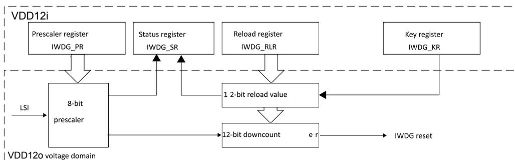
Note: The watchdog is implemented in the VDD12o power domain that is still functional in Deepstop mode.
20.4 IWDG registers
Refer to Table 2. Acronyms for a list of abbreviations used in register descriptions. The peripheral registers can be accessed by half-words (16-bit) or words (32-bit).
20.4.1 Key register (IWDG_KR)
Address offset: 0x00
Reset value: 0x0000 0000
| 31 | 30 | 29 | 28 | 27 | 26 | 25 | 24 | 23 | 22 | 21 | 20 | 19 | 18 | 17 | 16 |
| Res. | Res. | Res. | Res. | Res. | Res. | Res. | Res. | Res. | Res. | Res. | Res. | Res. | Res. | Res. | Res. |
| 15 | 14 | 13 | 12 | 11 | 10 | 9 | 8 | 7 | 6 | 5 | 4 | 3 | 2 | 1 | 0 |
| KEY[15:0] | |||||||||||||||
| w | w | w | w | w | w | w | w | w | w | w | w | w | w | w | w |
| Bits 31:16 | Reserved, must be kept at reset value. |
| Bits 15:0 | KEY[15:0]: Key value (write only, read 0x0000). These bits must be written by software at regular intervals with the key value 0xAAAA, otherwise the watchdog generates a reset when the counter reaches 0. Writing the key value 0x5555 enables access to the IWDG_PR, IWDG_RLR and IWDG_WINR registers (see Section 20.3.2: Register access protection). Writing the key value CCCCh starts the watchdog (except if the hardware watchdog option is selected). |
20.4.2 Prescaler register (IWDG_PR)
Address offset: 0x04
Reset value: 0x0000 0000
| 31 | 30 | 29 | 28 | 27 | 26 | 25 | 24 | 23 | 22 | 21 | 20 | 19 | 18 | 17 | 16 |
|---|---|---|---|---|---|---|---|---|---|---|---|---|---|---|---|
| Res. | Res. | Res. | Res. | Res. | Res. | Res. | Res. | Res. | Res. | Res. | Res. | Res. | Res. | Res. | Res. |
| 15 | 14 | 13 | 12 | 11 | 10 | 9 | 8 | 7 | 6 | 5 | 4 | 3 | 2 | 1 | 0 |
| Res. | Res. | Res. | Res. | Res. | Res. | Res. | Res. | Res. | Res. | Res. | Res. | Res. | rw | rw | rw |
| Bits 31:3 | Reserved, must be kept at reset value. |
| Bits 2:0 | PR[2:0]: Prescaler divider. These bits are write access protected, see Section 20.3.2: Register access protection . They are written by software to select the prescaler divider feeding the counter clock. PVU bit of IWDG_SR must be reset in order to be able to change the prescaler divider. 000: divider /4 Note: Reading this register returns the prescaler value from the VDD12o voltage domain. This value may not be up to date/valid if a write operation to this register is on-going. For this reason the value read from this register is valid only when the PVU bit in the IWDG_SR register is reset. |
20.4.3 Reload register (IWDG_RLR)
Address offset: 0x08
Reset value: 0x0000 0FFF
| 31 | 30 | 29 | 28 | 27 | 26 | 25 | 24 | 23 | 22 | 21 | 20 | 19 | 18 | 17 | 16 |
|---|---|---|---|---|---|---|---|---|---|---|---|---|---|---|---|
| Res. | Res. | Res. | Res. | Res. | Res. | Res. | Res. | Res. | Res. | Res. | Res. | Res. | Res. | Res. | Res. |
| 15 | 14 | 13 | 12 | 11 | 10 | 9 | 8 | 7 | 6 | 5 | 4 | 3 | 2 | 1 | 0 |
| Res. | Res. | Res. | Res. | rw | rw | rw | rw | rw | rw | rw | rw | rw | rw | rw | rw |
| Bits 31:12 | Reserved, must be kept at reset value. |
| Bits 11:0 | RL[11:0]: Watchdog counter reload value. These bits are write access protected, see Section 20.3.2: Register access protection . They are written by software to define the value to be loaded in the watchdog counter each time the value 0xAAAA is written in the IWDG_KR register. The watchdog counter counts down from this value. The timeout period is a function of this value and the clock prescaler. Refer to the datasheet for the timeout information. The RVU bit in the IWDG_SR register must be reset in order to be able to change the reload value. Note: Reading this register returns the reload value from the VDD12o voltage domain. This value may not be up to date/valid if a write operation to this register is on-going on this register. For this reason the value read from this register is valid only when the RVU bit in the IWDG_SR register is reset. |
20.4.4 Status register (IWDG_SR)
Address offset: 0x0C
Reset value: 0x0000 0000
| 31 | 30 | 29 | 28 | 27 | 26 | 25 | 24 | 23 | 22 | 21 | 20 | 19 | 18 | 17 | 16 |
| Res. | Res. | Res. | Res. | Res. | Res. | Res. | Res. | Res. | Res. | Res. | Res. | Res. | Res. | Res. | Res. |
| 15 | 14 | 13 | 12 | 11 | 10 | 9 | 8 | 7 | 6 | 5 | 4 | 3 | 2 | 1 | 0 |
| Res. | Res. | Res. | Res. | Res. | Res. | Res. | Res. | Res. | Res. | Res. | Res. | Res. | WVU | RVU | PVU |
| r | r | r |
| Bits 31:3 | Reserved, must be kept at reset value. |
| Bit 2 | WVU: Watchdog counter window value update. This bit is set by hardware to indicate that an update of the window value is on-going. It is reset by hardware when the reload value update operation is completed in the VDD12o voltage domain (takes up to 5 RC 40 kHzcycles). Window value can be updated only when WVU bit is reset. This bit is generated only if generic "window" = 1. |
| Bit 1 | RVU: Watchdog counter reload value update. This bit is set by hardware to indicate that an update of the reload value is on-going. It is reset by hardware when the reload value update operation is completed in the VDD12o voltage domain (takes up to 5 RC 40 kHzcycles). Reload value can be updated only when RVU bit is reset. |
| Bit 0 | PVU: Watchdog prescaler value update. This bit is set by hardware to indicate that an update of the prescaler value is on-going. It is reset by hardware when the prescaler update operation is completed in the VDD12o voltage domain (takes up to 5 RC 40 kHz cycles). Prescaler value can be updated only when PVU bit is reset. |
20.4.5 Window register (IWDG_WINR)
Address offset: 0x10
Reset value: 0x0000 0FFF
| 31 | 30 | 29 | 28 | 27 | 26 | 25 | 24 | 23 | 22 | 21 | 20 | 19 | 18 | 17 | 16 |
|---|---|---|---|---|---|---|---|---|---|---|---|---|---|---|---|
| Res. | Res. | Res. | Res. | Res. | Res. | Res. | Res. | Res. | Res. | Res. | Res. | Res. | Res. | Res. | Res. |
| 15 | 14 | 13 | 12 | 11 | 10 | 9 | 8 | 7 | 6 | 5 | 4 | 3 | 2 | 1 | 0 |
| Res. | Res. | Res. | Res. | WIN[11:0] | |||||||||||
| rw | rw | rw | rw | rw | rw | rw | rw | rw | rw | rw | rw | ||||
| Bits 31:12 | Reserved, must be kept at reset value. |
| Bits 11:0 | WIN[11:0]: Watchdog counter window value. These bits are write access protected, see Section 20.3.2: Register access protection . These bits contain the high limit of the window value to be compared to the down-counter. To prevent a reset, the down-counter must be reloaded when its value is lower than the window register value and greater than 0x0. The WVU bit in the IWDG_SR register must be reset in order to be able to change the reload value. Note: Reading this register returns the reload value from the VDD12o voltage domain. This value may not be valid if a write operation to this register is on-going. For this reason the value read from this register is valid only when the WVU bit in the IWDG_SR register is reset. |
Note:
If several reload, prescaler, or window values are used by the application, it is mandatory to wait for the RVU bit to be reset before changing the reload value, to wait for the PVU bit to be reset before changing the prescaler value, and to wait for the WVU bit to be reset before changing the window value. However, after updating the prescaler and/or the reload/window value it is not necessary to wait for RVU or PVU or WVU to be reset before continuing code execution except in case of low-power mode entry.
20.4.6 IWDG register map
The following table gives the IWDG register map and reset values.
Table 84. IWDG register map
| Offset | Register | 31 | 30 | 29 | 28 | 27 | 26 | 25 | 24 | 23 | 22 | 21 | 20 | 19 | 18 | 17 | 16 | 15 | 14 | 13 | 12 | 11 | 10 | 9 | 8 | 7 | 6 | 5 | 4 | 3 | 2 | 1 | 0 | |
|---|---|---|---|---|---|---|---|---|---|---|---|---|---|---|---|---|---|---|---|---|---|---|---|---|---|---|---|---|---|---|---|---|---|---|
| 0x00 | IWDG_KR | Res. | Res. | Res. | Res. | Res. | Res. | Res. | Res. | Res. | Res. | Res. | Res. | Res. | Res. | Res. | Res. | KEY[15:0] | ||||||||||||||||
| Reset value | 0 | 0 | 0 | 0 | 0 | 0 | 0 | 0 | 0 | 0 | 0 | 0 | 0 | 0 | 0 | |||||||||||||||||||
| 0x04 | IWDG_PR | Res. | Res. | Res. | Res. | Res. | Res. | Res. | Res. | Res. | Res. | Res. | Res. | Res. | Res. | Res. | Res. | Res. | Res. | Res. | Res. | Res. | Res. | Res. | Res. | Res. | Res. | Res. | Res. | Res. | Res. | PR[2:0] | ||
| Reset value | 0 | 0 | 0 | |||||||||||||||||||||||||||||||
| 0x08 | IWDG_RLR | Res. | Res. | Res. | Res. | Res. | Res. | Res. | Res. | Res. | Res. | Res. | Res. | Res. | Res. | Res. | Res. | Res. | Res. | Res. | Res. | RL[11:0] | ||||||||||||
| Reset value | 1 | 1 | 1 | 1 | 1 | 1 | 1 | 1 | 1 | 1 | 1 | 1 | ||||||||||||||||||||||
| 0x0C | IWDG_SR | Res. | Res. | Res. | Res. | Res. | Res. | Res. | Res. | Res. | Res. | Res. | Res. | Res. | Res. | Res. | Res. | Res. | Res. | Res. | Res. | Res. | Res. | Res. | Res. | Res. | Res. | Res. | Res. | Res. | Res. | WVU | RVU | PVU |
| Reset value | 0 | 0 | 0 | |||||||||||||||||||||||||||||||
| 0x08 | IWDG_WINR | Res. | Res. | Res. | Res. | Res. | Res. | Res. | Res. | Res. | Res. | Res. | Res. | Res. | Res. | Res. | Res. | Res. | Res. | Res. | Res. | WIN[11:0] | ||||||||||||
| Reset value | 1 | 1 | 1 | 1 | 1 | 1 | 1 | 1 | 1 | 1 | 1 | 1 | ||||||||||||||||||||||
Refer to Section 2.2.2: Memory map and register boundary addresses for the register boundary addresses.