12. Analog digital converter (ADC)
The STM32WB05xZ embeds a 12-bit ADC. The ADC consists of a 12-bit successive approximation analog-to-digital converter (SAR) with 2 x 8 multiplexed channels allowing measurements of up to eight external sources and up to two internal sources.
12.1 Features
- • Conversion frequency is up to 1 Msps
- • Three input voltage ranges are supported (0 → 1.2 V, 0 → 2.4 V, 0 → 3.6 V)
- • Up to eight analog single-ended channels or four analog differential inputs or a mix of both
- • Temperature sensor conversion
- • Battery level conversion up to 3.6 V
- • Continuous or single acquisition
- • ADC mode conversion only available, programmable in continuous or single mode
- • ADC down sampler for multi-purpose applications to improve analog performance while off-loading the CPU (ratio adjustable from 1 to 128)
- • A watchdog feature to inform when data is outside thresholds
- • DMA capability
- • Interrupt sources with flags.
12.2 ADC presentation
Figure 22. ADC top level diagram shows the top level diagram of the ADC.
The analog ADC can be configured to interface with the following inputs:
- • External signals through ADC_VINPx and ADC_VINMx, where x = 0,1,2 or 3
- – Up to 4 differential inputs
- – Up to 8 single-ended inputs
- • Temperature sensor
- • Battery level detector up to 3.6 V
Figure 22. ADC top level diagram
![ADC top level diagram showing the internal architecture of the ADC subsystem. It includes input channels (VDDA, GND, TEMP SENSOR, VBAT, SELN_VINP[3:0], SELN_VINM[3:0], VINP, VINM) connected to a Muxing block. The Muxing block feeds into a SAR ADC 12bits block, which is connected to a Reference block. The SAR ADC output (12 bits) goes to an ADC Offset Correction and Bit Inversion block. This block feeds into a Down Sampler (16 bits) and a TO ADC WATCHDOG block. The Down Sampler output (16 bits) goes to a DATA REG1 block. The DATA REG1 block is connected to an APB MEMORY PORT. The APB MEMORY PORT is connected to an APB bus, which is connected to a CPU or DMA to RAM. The APB bus also connects to a Digital ADC Subsystem and an Analog ADC Subsystem. The Digital ADC Subsystem contains a CONF REG, CONTROL REG, WD TRIG REG, INT REG, and STATUS REG. The Analog ADC Subsystem contains a WD Block and a Sequencer Block. The WD Block and Sequencer Block are connected to the APB bus. The INT REG is connected to an INT to CPU block. The DATA REG1 block is also connected to a DREQ1 block. The DREQ1 block is connected to the APB bus. The APB bus is labeled 'APB'.](/RM0529-STM32WB05xZ/c36c9f3fd6dfe6c3116a5b86b6ab0877_img.jpg)
The input of the data path can come from the analog ADC through the possible inputs mentioned previously. The conversion data path can go through a downsampler (for static or low frequency input signals).
Caution: Do not change the configuration registers related to the function in use. Any change done by the user on the different bits are applied immediately, with an immediate effect on the on-going process (conversion, decimator filter or downsampler). This action can lead to unexpected results.
For VBAT < 2.7 V, the IO booster needs to be activated to maintain linearity.
12.2.1 Temperature sensor subsystem
The temperature sensor can be used to measure the junction temperature ( \( T_j \) ) of the device. The temperature sensor is internally connected to the ADC input channels, which are used to convert the sensor output voltage to a digital value.
The temperature sensor output voltage changes linearly with temperature. The offset of this line varies from chip-to-chip due to process variation. The uncalibrated internal temperature sensor is more suited for applications that detect temperature variations instead of absolute temperatures. To improve the accuracy of the temperature sensor measurement, calibration values are stored in system memory for each device by ST during production. During the manufacturing process, the calibration data of the temperature sensor and the internal voltage reference are stored in the system memory area. The user application can then read them and use them to improve the accuracy of the temperature sensor or the internal reference. In this way the temperature can be calculated with this formula:
Where:
TCK is the chuck temperature in 0.1 °C (e.g. 30 °C = 300) readable @0x10001E5C.
C30 is the temperature sensor calibration value acquired at 30 °C readable @0x10001E60.
Cmeas is the actual temperature sensor output value converted by ADC.
Note: ADC gain and offset calibration are left as default values, 0xFFF.
Note: Refer to Section 27: Device electronic signature (DESIG) for information about the location where these calibration values are stored.
12.2.2 Battery sensor
The battery sensor can be used to measure the internal battery voltage of the device. The battery input is internally connected to the ADC input channels which are used to convert the sensor output voltage to a digital value.
The battery sensor range is up to 3.6 V.
The formula for ADC converted data after calibration is the following:
Code = Integer(4096/3.6 * VIN) [clamped at 4095]
As calibration points the VBAT is considered as single negative input with 3.6 V range.
Note: Refer to Section 27.1: DESIG registers for information about the location where these calibration values are stored.
12.2.3 ADC input mode conversion
The ADC is designed to deliver a digital value corresponding to the ratio between the voltage applied on the converted channel and the reference voltage, VDDA. Note that VDDA is also the ADC's power supply.
The formula for ADC digital converted data after calibration and offset is the following:
- • Single-ended input mode
Code = Integer(Slope* VIN) [clamped at 4095]
where Slope for single-ended input mode has the following value:
3.6 V mode: Slope = 4096/3.6 [calibrated gain = 1/3]
2.4 V mode: Slope = 4096/2.4 [calibrated gain = 1/2]
1.2 V mode: Slope = 4096/1.25 [calibrated gain = 0.96, gain clamped at 1] - • Differential input mode
Code = Integer(Slope * (VINP - VINN)) + 2048 [clamped at 4095]
where Slope for differential input mode has the following value:
3.6 V mode: Slope = 2048/3.6 [calibrated gain = 1/3]
2.4 V mode: Slope = 2048/2.4 [calibrated gain = 1/2]
1.2 V mode: Slope = 2048/1.25 [calibrated gain = 0.96, gain clamped at 1]
12.2.4 Steady-state input impedance
As the input nature of the ADC is a switched-capacitor, its steady-state input impedance is defined as the impedance seen in DC. It depends only on the analog sampling frequency, Fs, and the input capacitor, Cin: \( Z_{in} = 1/(C_{in} \cdot F_s) \) .
12.2.5 Input signal sampling transient response
As represented in Figure 24. Effect of analog source resistance , the analog signal path consists of a series resistance (Rext) between source and pin, the internal switch resistor (Rin), and the internal sampling capacitor (Cin). The charging of the capacitor is controlled by Rin. When there is Rext in series, the effective value of charging of Cin is governed by Rin+Rext. So, the charging time constant becomes (Rin+Rext)*Cin and the necessary time to reach a given accuracy is longer. The ADC's sampling time, Tsw, is a function of the ADC's frequency, 1/Ts as follows:
Figure 23. ADC sampling time Tsw and sampling period Ts
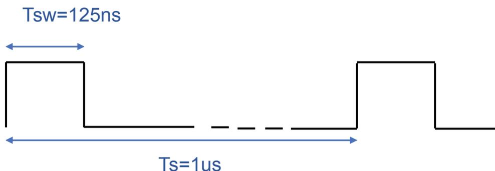
The diagram shows a square wave representing the ADC sampling signal. A horizontal double-headed arrow at the top indicates the sampling time \( T_{sw} = 125\text{ns} \) , which corresponds to the duration of the high state. A horizontal double-headed arrow at the bottom indicates the sampling period \( T_s = 1\text{us} \) , which corresponds to the duration of one full cycle (high + low).
Figure 24. Effect of analog source resistance
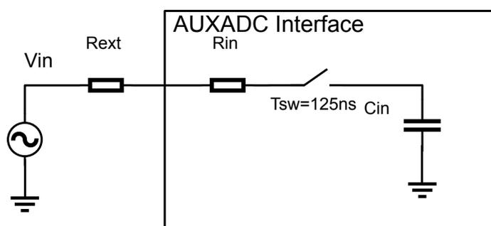
The diagram illustrates the equivalent circuit for an ADC input. An external voltage source \( V_{in} \) is connected to the ADC input through an external source resistance \( R_{ext} \) . Inside the 'AUXADC Interface', there is an internal input resistance \( R_{in} \) . A switch, representing the sampling switch, is shown in series with \( R_{in} \) . This switch has a sampling time \( T_{sw} = 125\text{ns} \) . Following the switch, there is an internal sampling capacitance \( C_{in} \) connected to ground.
Knowing that: \( R_{in} = 550\ \Omega \) , \( C_{in} = 4\ \text{pF} \) , and imposing a maximum sampling error of 1/2 bits, we can determine the maximum input resistance as below:
Where:
12.2.6 Calibration points
Calibration values are stored in the system memory for each device by ST during production. Each value consists of a 12-bit unsigned value for the gain and an 8-bit signed value for the offset as follows:
OFFSET[18:12] | GAIN[11:0]
These values can be written inside the registers COMP_x with \( x = 1, 2, 3, 4 \) to apply a point to a particular ADC input. The COMP_SEL register allows a specific calibration point to be associated to one of the ADC inputs.
The offset value can be written inside the COMP_x register only if it fits in the 7-bit of register field, that means offset is in [-64, 63]. Otherwise, it can be removed by the output raw data manually as \( \text{raw\_value} + \text{offset} \) .
The negative offset values need to be converted as:
offset | 0x80, if the bitfield BIT_INVERT_SN=1 (default value).
Below the list of the calibration points and their location in the system memory.
Table 31. Calibration points
| Calibration point | Address location |
|---|---|
| VINPx - VINMx range 1.2 V | 0x10001E00 |
| VINMx range 1.2 V | 0x10001E04 |
| VINPx range 1.2 V | 0x10001E08 |
| VINPx - VINMx range 2.4 V | 0x10001E0C |
| VINMx range 2.4 V | 0x10001E10 |
| VINPx range 2.4 V | 0x10001E14 |
| VINPx - VINMx range 3.6 V | 0x10001E18 |
| VINMx range 3.6 V | 0x10001E1C |
| VINPx range 3.6 V | 0x10001E20 |
Note: Previous version of the calibration points has the offset in 7-bit signed. This version can be recognized as the user can read at address 0x10001EFC the value 0.
Note: Refer to Section 27.1: DESIG registers for information about the location where these calibration values are stored.
12.2.7 Down sampler (DS)
This down sampler is a simple averaging filter, which can divide the ADC frequency by 1 to 128 by power of 2. The goal is to handle multiple ADC samples and average them into a single data with increased data width ranging from 12-bit to 16-bit.
The down sampler increases the data precision but reduces the output data rate.
Note: A constraint on the ratio between APB system clock ( \( F_{PCLK} \) ) and the output data rate ( \( DR_{out} \) ) must be respected:
- • In ADC mode, the ratio to respect is \( F_{PCLK} / DR_{out} \geq 4 \) .
Example: \( F_{PCLK} \) must be at least 2 MHz to have a \( DR_{out} = 500 \) kHz.
If the DMA is not used to get the data output by the down sampler filter path, the CPU needs to be clocked at a frequency ratio high enough (taking into account bus matrix latency) to avoid missing samples.
12.3 Interrupts
There are 5 maskable interrupts generated by the ADC block. These interrupts are combined to produce one single interrupt output, which is the only interrupt line from the ADC to the CPU.
Table 32. ADC interrupt requests
| Interrupt event | Event flag | Interrupt / flag clearing method | Interrupt enable control bit |
|---|---|---|---|
| ADC end of Conversion (Test mode only) | EOC_IRQ | Write 1 on EOC_IRQ bit | EOC_IRQ_ENA |
| Down sampler end of conversion | EODS_IRQ | Write 1 on EODS_IRQ bit | EODS_IRQ_ENA |
| End of conversion sequence | EOS_IRQ | Write 1 on EOS_IRQ bit | EOS_IRQ_ENA |
| Analog watchdog event | AWD_IRQ | Write 1 on AWD_IRQ bit | AWD_IRQ_ENA |
| Down sampler overrun | OVR_DS_IRQ | Write 1 on OVR_DS_IRQ bit | OVR_DS_IRQ_ENA |
12.4 DMA interface
The ADC has one DMA channel interface to get down sampler data output value.
The DMA feature is enabled by software through the CONF register by DMA_DS_ENA bit.
When DMA feature is disabled, the CPU reads the data through the corresponding APB register.
12.5 ADC mode
ADC is the only conversion mode available for STM32WB05xZ.
The input signal can come from:
- • 8 single external channels (or 4 when coupled as differential)
- • VBAT
- • Temperature sensor
The conversion can be continuous or single mode.
Table 33. ADC mode summary
| Mode | Input signal | DS (1) | Continuous or single |
|---|---|---|---|
| ADC |
| DS | Continuous or single |
1. Down Sampler
12.5.1 ADC mode overview
Presentation
The ADC mode has the following characteristics:
- • The input in the ADC mode can be the eight external channels and the two internal sources (VBAT and temperature sensor)
- • The data path goes from the ADC to the down sampler
- • The converted data is output in the DS_DATAOUT register
- • The output data rates are in the range 117 ksps to 1 Msps
- • The 12-bit converted data can be extended up to 16-bit data thanks to the down sampler. However, in this case, the output data rate is decreased
- • A regular sequence of conversion can be executed in single of continuous mode
- – A regular sequence consists of chaining ADC conversions on any ADC input channel and in any order.
- – A regular sequence can chain up to 16 conversions.
- – The source of the input for each conversion of the sequence is selected through SEQx bit field in SEQ_1 and SEQ_2 registers.
- – This regular sequence can be run once or repeated continuously by setting the CONT bit in the CONF register.
ADC mode usage
This paragraph describes the process to use the ADC mode:
- • Power-on the ADC if not yet done by setting the ADC_ON_OFF bit in the CTRL register
- • Program the targeted data rate through SAMPLE_RATE and DS_CONF registers
- • Program the input voltage selections through the SWITCH register
- • Program the COMP_1 to COMP_4 and the COMP_SEL registers
- • Program the targeted regular sequence (up to 16 chained conversions) through SEQ_1 and SEQ_2 registers
- • Specify the length of the sequence in SEQ_LEN bit field in CONF (from 0 for one conversion to 0xF for sixteen conversions).
Note: To have more than one conversion, ensure the bit SEQUENCE is well at 1 in CONF register.
- • Program the CONT bit and the SEQ_LEN bit field in the CONF register, considering SEQUENCE bit is always set) depending on the wished sequence:
- – CONT = 0 and SEQ_LEN = 0 to have a single conversion on a single channel.
- – CONT = 0 and SEQ_LEN > 0 to have a single run of a sequence chaining several conversions on different channels/sources.
- – CONT = 1 and SEQ_LEN = 0 to have a continuous conversion of a single channel/source.
- – CONT = 1 and SEQ_LEN > 0 to have a continuous run of sequence chaining several conversions on different channels/sources.
- • Launch the programmed regular sequence by setting the START_CONV bit in CTRL register
- • Each time a data is available at the output of the down sampler, the data is stored in the DS_DATAOUT register and the EODS flag is set (as analog mode goes through the down sampler)
- • To get the converted values:
- – Either the DMA is enabled on DS data path (through DMA_DS_ENA bit in CONF register) and DMA copies the converted data in RAM at the end of each data conversion
- – Or the software has enabled the EODS_IRQ interrupt and is able to get the data from DS_DATAOUT register before a new converted data is generated.
Note: If the CPU does not manage to get the converted data before a new converted data is generated, the OVR_DS_IRQ flag is raised to inform a data has been lost. The software can program the hardware behavior in case of overrun through the OVR_DS_CFG bit in CONF register:
- • If 0, the previous data is kept, the new one is lost.
- • If 1, the previous data is lost, the new one is kept.
- • Each time the regular sequence is completed, the EOS_IRQ flag is raised (and may generate an interrupt if enabled)
- • If the sequence is a single sequence (CONT=0), the ADC stops at the end of the sequence and does not restart until START_CONV bit is not set again
- • If continuous conversion is enabled (CONT = 1), the ADC restarts a new sequence, and data conversion continues until the software stops it by setting the STOP_OP_MODE bit in the CTRL register. In this case, the ADC stops immediately, and the data from any ongoing conversion is discarded
12.6 ADC registers
12.6.1 Version register (VERSION_ID)
Address offset: 0x00
Reset value: 0x0000 0030
| 31 | 30 | 29 | 28 | 27 | 26 | 25 | 24 | 23 | 22 | 21 | 20 | 19 | 18 | 17 | 16 |
| Res. | Res. | Res. | Res. | Res. | Res. | Res. | Res. | Res. | Res. | Res. | Res. | Res. | Res. | Res. | Res. |
| 15 | 14 | 13 | 12 | 11 | 10 | 9 | 8 | 7 | 6 | 5 | 4 | 3 | 2 | 1 | 0 |
| Res. | Res. | Res. | Res. | Res. | Res. | Res. | Res. | VERSION_ID[7:0] | |||||||
| r | r | r | r | r | r | r | r | ||||||||
| Bits 31:8 | Reserved, must be kept at reset value. |
| Bit 7:0 | VERSION_ID[7:0] : Version of the embedded IP. |
12.6.2 ADC configuration register (CONF)
Address offset: 0x04
Reset value: 0x0002 0002
| 31 | 30 | 29 | 28 | 27 | 26 | 25 | 24 | 23 | 22 | 21 | 20 | 19 | 18 | 17 | 16 |
| Res. | Res. | Res. | Res. | Res. | Res. | Res. | Res. | SAMPLE_RATE_MSB | ADC_CONT_1V2 | BIT_INVERT_DIFF | BIT_INVERT_SN | ||||
| rw | rw | rw | rw | ||||||||||||
| 15 | 14 | 13 | 12 | 11 | 10 | 9 | 8 | 7 | 6 | 5 | 4 | 3 | 2 | 1 | 0 |
| OVR_DS_CFG | Res. | DMA_DS_ENA | SAMPLE_RATE[1:0] | Res. | Res. | Res. | Res. | SMPS_SYNCHRO_ENA | SEQ_LEN[3:0] | ||||||
| rw | rw | rw | rw | rw | rw | rw | |||||||||
| Bits 31:24 | Reserved, must be kept at reset value. |
| Bits 23:21 | SAMPLE_RATE_MSB
: Sample Rate MSB This field is an extension of SAMPLE_RATE definition in bits 12,11 of CONF register. It impacts the conversion rate of ADC (F_ADC). See SAMPLE_RATE bits for the full description. |
| Bit 20 | Reserved, must be kept at reset value. |
| Bit 19 | ADC_CONT_1V2
: Select the input sampling method:
|
| Bit 18 | BIT_INVERT_DIFF:
Invert bit-to-bit the ADC data output (1's complement) when a differential input is connected to the ADC:
|
| Bit 17 | BIT_INVERT_SN:
Invert bit-to-bit the ADC data output (1's complement) when a single negative input is connected to the ADC:
|
| Bit 16 | Reserved, must be kept at reset value. |
| Bit 15 | OVR_DS_CFG:
Down sampler overrun configuration:
|
| Bit 14 | Reserved, must be kept at reset value. |
| Bit 13 | DMA_DS_EN:
Enable the DMA mode for the down sampler data path:
|
| Bits 12:11 | SAMPLE_RATE[1:0]:
Conversion rate of ADC (
\(
F\_ADC
\)
): \( F\_ADC = F\_ADC\_CLK / (16 + 16 * \text{SAMPLE\_RATE\_MSB} + 4 * \text{SAMPLE\_RATE}) \) , where \( F\_ADC\_CLK \) is the analog ADC clock frequency. By default \( F\_ADC\_CLK \) is 16MHz frequency. |
| Bits 10:7 | Reserved, must be kept at reset value. |
| Bit 6 | SMPS_SYNCHRO_ENA:
Synchronize the ADC start conversion with a pulse generated by the SMPS:
|
| Bits 5:2 | SEQ_LEN[3:0]:
Number of conversions in a regular sequence:
|
| Bit 1 | SEQUENCE:
Enable the sequence mode (active by default):
|
| Bit 0 | CONT:
Regular sequence runs continuously when ADC mode is enabled:
|
12.6.3 ADC control register (CTRL)
Address offset: 0x08
Reset value: 0x0000 0000
| 31 | 30 | 29 | 28 | 27 | 26 | 25 | 24 | 23 | 22 | 21 | 20 | 19 | 18 | 17 | 16 |
|---|---|---|---|---|---|---|---|---|---|---|---|---|---|---|---|
| Res. | Res. | Res. | Res. | Res. | Res. | Res. | Res. | Res. | Res. | Res. | Res. | Res. | Res. | Res. | Res. |
| 15 | 14 | 13 | 12 | 11 | 10 | 9 | 8 | 7 | 6 | 5 | 4 | 3 | 2 | 1 | 0 |
| Res. | Res. | Res. | Res. | Res. | Res. | Res. | Res. | Res. | Res. | ADC_LDO_ENA | Res. | Res. | STOP_OP_MODE | START_CONV | ADC_ON_OFF |
| rw | rw | t | t | rw |
| Bits 31:6 | Reserved, must be kept at reset value. |
| Bit 5 | ADC_LDO_ENA
: Enable the LDO associated to the ADC block:
|
| Bit 4 | Reserved, must be kept at reset value. |
| Bit 3 | Reserved, must be kept at reset value. |
| Bit 2 | STOP_OP_MODE
(1)
: Stop the on-going ADC mode:
|
| Bit 1 | START_CONV
(1)
: Generates a start pulse to initiate an ADC conversion:
|
| Bit 0 | ADC_ON_OFF
:
|
- 1. When setting the STOP_MODE_OP , the user has to wait around 10 µs before starting a new ADC conversion by setting the START_CONV bit.
12.6.4 ADC input voltage switch selection register (SWITCH)
Address offset: 0x14
Reset value: 0x0000 0000
| 31 | 30 | 29 | 28 | 27 | 26 | 25 | 24 | 23 | 22 | 21 | 20 | 19 | 18 | 17 | 16 |
| Res. | Res. | Res. | Res. | Res. | Res. | Res. | Res. | Res. | Res. | Res. | Res. | Res. | Res. | Res. | Res. |
| 15 | 14 | 13 | 12 | 11 | 10 | 9 | 8 | 7 | 6 | 5 | 4 | 3 | 2 | 1 | 0 |
| SE_VIN_7[1:0] | SE_VIN_6[1:0] | SE_VIN_5[1:0] | SE_VIN_4[1:0] | SE_VIN_3[1:0] | SE_VIN_2[1:0] | SE_VIN_1[1:0] | SE_VIN_0[1:0] | ||||||||
| rw | rw | rw | rw | rw | rw | rw | rw | rw | rw | rw | rw | rw | rw | rw | rw |
| Bits 31:16 | Reserved, must be kept at reset value. |
| Bits 15:14 | SE_VIN_7[1:0]
: Input voltage for VINP[3].
|
| Bits 13:12 | SE_VIN_6[1:0]
: Input voltage for VINP[2].
|
| Bits 11:10 | SE_VIN_5[1:0]
: Input voltage for VINP[1].
|
| Bits 9:8 | SE_VIN_4[1:0]
: Input voltage for VINP[0].
|
| Bits 7:6 | SE_VIN_3[1:0]
: Input voltage for VINM[3] / VINP[3]-VINM[3].
|
| Bits 5:4 | SE_VIN_2[1:0]
: Input voltage for VINM[2] / VINP[2]-VINM[2].
|
| Bits 3:2 | SE_VIN_1[1:0]
: Input voltage for VINM[1] / VINP[1]-VINM[1].
|
| Bits 1:0 | SE_VIN_0[1:0]
: Input voltage for VINM[0] / VINP[0]-VINM[0].
|
12.6.5 Down sampler configuration register (DS_CONF)
Address offset: 0x1C
Reset value: 0x0000 0000
| 31 | 30 | 29 | 28 | 27 | 26 | 25 | 24 | 23 | 22 | 21 | 20 | 19 | 18 | 17 | 16 |
| Res. | Res. | Res. | Res. | Res. | Res. | Res. | Res. | Res. | Res. | Res. | Res. | Res. | Res. | Res. | Res. |
| 15 | 14 | 13 | 12 | 11 | 10 | 9 | 8 | 7 | 6 | 5 | 4 | 3 | 2 | 1 | 0 |
| Res. | Res. | Res. | Res. | Res. | Res. | Res. | Res. | Res. | Res. | DS_WIDTH[2:0] | DS_RATIO[2:0] | ||||
| rw | rw | rw | rw | rw | rw | ||||||||||
| Bits 31:6 | Reserved, must be kept at reset value. |
| Bits 5:3 | DS_WIDTH[2:0]:
Program the down sampler width of data output (DSDATA).
|
| Bits 2:0 | DS_RATIO[2:0]:
Program the down sampler ratio (N factor).
|
12.6.6 ADC sequence programming 1 register (SEQ_1)
Address offset: 0x20
Reset value: 0x0000 0000
| 31 | 30 | 29 | 28 | 27 | 26 | 25 | 24 | 23 | 22 | 21 | 20 | 19 | 18 | 17 | 16 |
| SEQ7[3:0] | SEQ6[3:0] | SEQ5[3:0] | SEQ4[3:0] | ||||||||||||
| rw | rw | rw | rw | rw | rw | rw | rw | rw | rw | rw | rw | rw | rw | rw | rw |
| 15 | 14 | 13 | 12 | 11 | 10 | 9 | 8 | 7 | 6 | 5 | 4 | 3 | 2 | 1 | 0 |
| SEQ3[3:0] | SEQ2[3:0] | SEQ1[3:0] | SEQ0[3:0] | ||||||||||||
| rw | rw | rw | rw | rw | rw | rw | rw | rw | rw | rw | rw | rw | rw | rw | rw |
| Bits 31:28 | SEQ7[3:0]
: Channel number code for 8
th
conversion of the sequence. See SEQ0 for code detail. |
| Bits 27:24 | SEQ6[3:0] : Channel number code for 7 th conversion of the sequence. See SEQ0 for code detail. |
| Bits 23:20 | SEQ5[3:0] : Channel number code for 6 th conversion of the sequence. See SEQ0 for code detail. |
| Bits 19:16 | SEQ4[3:0] : Channel number code for 5 th conversion of the sequence. See SEQ0 for code detail. |
| Bits 15:12 | SEQ3[3:0] : Channel number code for 4 th conversion of the sequence. See SEQ0 for code detail. |
| Bits 11:8 | SEQ2[3:0] : Channel number code for 3 rd conversion of the sequence. See SEQ0 for code detail. |
| Bits 7:4 | SEQ1[3:0] : Channel number code for second conversion of the sequence. See SEQ0 for code detail. |
| Bits 3:0 | SEQ0[3:0]
: Channel number code for first conversion of the sequence
|
12.6.7 ADC sequence programming 2 register (SEQ_2)
Address offset: 0x24
Reset value: 0x0000 0000
| 31 | 30 | 29 | 28 | 27 | 26 | 25 | 24 | 23 | 22 | 21 | 20 | 19 | 18 | 17 | 16 |
| SEQ15[3:0] | SEQ14[3:0] | SEQ13[3:0] | SEQ12[3:0] | ||||||||||||
| rw | rw | rw | rw | rw | rw | rw | rw | rw | rw | rw | rw | rw | rw | rw | rw |
| 15 | 14 | 13 | 12 | 11 | 10 | 9 | 8 | 7 | 6 | 5 | 4 | 3 | 2 | 1 | 0 |
| SEQ11[3:0] | SEQ10[3:0] | SEQ9[3:0] | SEQ8[3:0] | ||||||||||||
| rw | rw | rw | rw | rw | rw | rw | rw | rw | rw | rw | rw | rw | rw | rw | rw |
| Bits 31:28 | SEQ15[3:0] : Channel number code for 16 th conversion of the sequence. See SEQ8 for code detail. |
| Bits 27:24 | SEQ14[3:0] : Channel number code for 15 th conversion of the sequence. See SEQ8 for code detail. |
| Bits 23:20 | SEQ13[3:0] : Channel number code for 14 th conversion of the sequence. See SEQ8 for code detail. |
| Bits 19:16 | SEQ12[3:0] : Channel number code for 13 th conversion of the sequence. See SEQ8 for code detail. |
| Bits 15:12 | SEQ11[3:0] : Channel number code for 12 th conversion of the sequence. See SEQ8 for code detail. |
| Bits 11:8 | SEQ10[3:0] : Channel number code for 11 th conversion of the sequence. See SEQ8 for code detail. |
| Bits 7:4 | SEQ9[3:0] : Channel number code for 10 th conversion of the sequence. See SEQ8 for code detail. |
| Bits 3:0 | SEQ8[3:0]
: Channel number code for 9
th
conversion of the sequence.
|
12.6.8 ADC gain and offset correction 1 register (COMP_1)
Address offset: 0x28
Reset value: 0x0000 0555
| 31 | 30 | 29 | 28 | 27 | 26 | 25 | 24 | 23 | 22 | 21 | 20 | 19 | 18 | 17 | 16 |
|---|---|---|---|---|---|---|---|---|---|---|---|---|---|---|---|
| Res. | Res. | Res. | Res. | Res. | Res. | Res. | Res. | Res. | Res. | Res. | Res. | OSFFSET1[7:4] | |||
| rw | rw | rw | rw | ||||||||||||
| 15 | 14 | 13 | 12 | 11 | 10 | 9 | 8 | 7 | 6 | 5 | 4 | 3 | 2 | 1 | 0 |
| OSFFSET1[3:0] | GAIN1[11:0] | ||||||||||||||
| rw | rw | rw | rw | rw | rw | rw | rw | rw | rw | rw | rw | rw | rw | rw | rw |
| Bits 31:20 | Reserved, must be kept at reset value. |
| Bits 19:12 | OFFSET1[7:0] : First calibration point: signed offset compensation[7:0]. |
| Bits 11:0 | GAIN1[11:0] : First calibration point: gain AUXADC_GAIN_1V2[11:0]. |
Note: Refer to Section 27: Device electronic signature (DESIG) for information about the location where these calibration values are stored.
12.6.9 ADC gain and offset correction 2 register (COMP_2)
Address offset: 0x2C
Reset value: 0x0000 0555
| 31 | 30 | 29 | 28 | 27 | 26 | 25 | 24 | 23 | 22 | 21 | 20 | 19 | 18 | 17 | 16 |
|---|---|---|---|---|---|---|---|---|---|---|---|---|---|---|---|
| Res. | Res. | Res. | Res. | Res. | Res. | Res. | Res. | Res. | Res. | Res. | Res. | OFFSET2[7:4] | |||
| rw | rw | rw | rw | rw | rw | rw | rw | rw | rw | rw | rw | rw | rw | rw | rw |
| 15 | 14 | 13 | 12 | 11 | 10 | 9 | 8 | 7 | 6 | 5 | 4 | 3 | 2 | 1 | 0 |
| OFFSET2[3:0] | GAIN2[11:0] | ||||||||||||||
| rw | rw | rw | rw | rw | rw | rw | rw | rw | rw | rw | rw | rw | rw | rw | rw |
| Bits 31:20 | Reserved, must be kept at reset value. |
| Bits 19:12 | OFFSET2[7:0] : Second calibration point: signed offset compensation[7:0]. |
| Bits 11:0 | GAIN2[11:0] : Second calibration point: gain AUXADC_GAIN_1V2[11:0]. |
Note: Refer to Section 27: Device electronic signature (DESIG) for information about the location where these calibration values are stored.
12.6.10 ADC gain and offset correction 3 register (COMP_3)
Address offset: 0x30
Reset value: 0x0000 0555
| 31 | 30 | 29 | 28 | 27 | 26 | 25 | 24 | 23 | 22 | 21 | 20 | 19 | 18 | 17 | 16 |
|---|---|---|---|---|---|---|---|---|---|---|---|---|---|---|---|
| Res. | Res. | Res. | Res. | Res. | Res. | Res. | Res. | Res. | Res. | Res. | Res. | OSFFSET3[7:4] | |||
| rw | rw | rw | rw | ||||||||||||
| 15 | 14 | 13 | 12 | 11 | 10 | 9 | 8 | 7 | 6 | 5 | 4 | 3 | 2 | 1 | 0 |
| OSFFSET3[3:0] | GAIN1[11:0] | ||||||||||||||
| rw | rw | rw | rw | rw | rw | rw | rw | rw | rw | rw | rw | rw | rw | rw | rw |
| Bits 31:20 | Reserved, must be kept at reset value. |
| Bits 19:12 | OFFSET3[7:0] : Third calibration point: signed offset compensation[7:0]. |
| Bits 11:0 | GAIN3[11:0] : Third calibration point: gain AUXADC_GAIN_1V2[11:0]. |
Note: Refer to Section 27: Device electronic signature (DESIG) for information about the location where these calibration values are stored.
12.6.11 ADC gain and offset correction 4 register (COMP_4)
Address offset: 0x34
Reset value: 0x0000 0555
| 31 | 30 | 29 | 28 | 27 | 26 | 25 | 24 | 23 | 22 | 21 | 20 | 19 | 18 | 17 | 16 |
|---|---|---|---|---|---|---|---|---|---|---|---|---|---|---|---|
| Res. | Res. | Res. | Res. | Res. | Res. | Res. | Res. | Res. | Res. | Res. | Res. | OSFFSET4[7:4] | |||
| rw | rw | rw | rw | ||||||||||||
| 15 | 14 | 13 | 12 | 11 | 10 | 9 | 8 | 7 | 6 | 5 | 4 | 3 | 2 | 1 | 0 |
| OSFFSET4[3:0] | GAIN1[11:0] | ||||||||||||||
| rw | rw | rw | rw | rw | rw | rw | rw | rw | rw | rw | rw | rw | rw | rw | rw |
| Bits 31:19 | Reserved, must be kept at reset value. |
| Bits 19:12 | OFFSET4[7:0] : Fourth calibration point: signed offset compensation[7:0]. |
| Bits 11:0 | GAIN4[11:0] : Fourth calibration point: gain AUXADC_GAIN_1V2[11:0]. |
Note: Refer to Section 27: Device electronic signature (DESIG) for information about the location where these calibration values are stored.
12.6.12 ADC gain and offset selection register (COMP_SEL)
Address offset: 0x38
Reset value: 0x0000 0000
| 31 | 30 | 29 | 28 | 27 | 26 | 25 | 24 | 23 | 22 | 21 | 20 | 19 | 18 | 17 | 16 |
|---|---|---|---|---|---|---|---|---|---|---|---|---|---|---|---|
| Res. | Res. | Res. | Res. | Res. | Res. | Res. | Res. | Res. | Res. | Res. | Res. | Res. | Res. | OFFSET_GAIN8[1:0] | |
| rw | rw | ||||||||||||||
| 15 | 14 | 13 | 12 | 11 | 10 | 9 | 8 | 7 | 6 | 5 | 4 | 3 | 2 | 1 | 0 |
| OFFSET_GAIN7[1:0] | OFFSET_GAIN6[1:0] | OFFSET_GAIN5[1:0] | OFFSET_GAIN4[1:0] | OFFSET_GAIN3[1:0] | OFFSET_GAIN2[1:0] | OFFSET_GAIN1[1:0] | OFFSET_GAIN0[1:0] | ||||||||
| rw | rw | rw | rw | rw | rw | rw | rw | rw | rw | rw | rw | rw | rw | rw | rw |
| Bits 31:18 | Reserved, must be kept at reset value. |
| Bits 17:16 | OFFSET_GAIN8[1:0]:
Gain / offset used in ADC differential mode with Vinput range = 3.6 V:
|
| Bits 15:14 | OFFSET_GAIN7[1:0]:
Gain / offset used in ADC single positive mode with Vinput range = 3.6 V:
|
| Bits 13:12 | OFFSET_GAIN6[1:0]:
Gain / offset used in ADC single negative mode with Vinput range = 3.6 V (this field also selects the gain/offset for VBAT input):
|
| Bits 11:10 | OFFSET_GAIN5[1:0]:
Gain / offset used in ADC differential mode with Vinput range = 2.4 V:
|
| Bits 9:8 | OFFSET_GAIN4[1:0]:
Gain / offset used in ADC single positive mode with Vinput range = 2.4 V:
|
| Bits 7:6 | OFFSET_GAIN3[1:0]:
Gain / offset used in ADC single negative mode with Vinput range = 2.4 V:
|
| |
| Bits 5:4 | OFFSET_GAIN2[1:0]:
Gain / offset used in ADC differential mode with Vinput range = 1.2 V:
|
| Bits 3:2 | OFFSET_GAIN1[1:0]:
Gain / offset used in ADC single positive mode with Vinput range = 1.2 V (this field also selects the gain/offset for temperature sensor input):
|
| Bits 1:0 | OFFSET_GAIN0[1:0]:
Gain / offset used in ADC single negative mode with Vinput range = 1.2 V:
|
12.6.13 ADC watchdog threshold register (WD_TH)
Address offset: 0x3C
Reset value: 0x0FFF 0000
| 31 | 30 | 29 | 28 | 27 | 26 | 25 | 24 | 23 | 22 | 21 | 20 | 19 | 18 | 17 | 16 |
| Res. | Res. | Res. | Res. | WD_HT[11:0] | |||||||||||
| rw | rw | rw | rw | rw | rw | rw | rw | rw | rw | rw | rw | ||||
| 15 | 14 | 13 | 12 | 11 | 10 | 9 | 8 | 7 | 6 | 5 | 4 | 3 | 2 | 1 | 0 |
| Res. | Res. | Res. | Res. | WD_LT[11:0] | |||||||||||
| rw | rw | rw | rw | rw | rw | rw | rw | rw | rw | rw | rw | ||||
| Bits 31:28 | Reserved, must be kept at reset value. |
| Bits 27:16 | WD_HT[11:0]: Analog watchdog high level threshold. |
| Bits 15:12 | Reserved, must be kept at reset value. |
| Bits 11:0 | WD_LT[11:0]: Analog watchdog low level threshold. |
12.6.14 ADC watchdog configuration register (WD_CONF)
Address offset: 0x40
Reset value: 0x0000 0000
| 31 | 30 | 29 | 28 | 27 | 26 | 25 | 24 | 23 | 22 | 21 | 20 | 19 | 18 | 17 | 16 |
| Res. | Res. | Res. | Res. | Res. | Res. | Res. | Res. | Res. | Res. | Res. | Res. | Res. | Res. | Res. | Res. |
| 15 | 14 | 13 | 12 | 11 | 10 | 9 | 8 | 7 | 6 | 5 | 4 | 3 | 2 | 1 | 0 |
| AWD_CHX[15:0] | |||||||||||||||
| r/w | r/w | r/w | r/w | r/w | r/w | r/w | r/w | r/w | r/w | r/w | r/w | r/w | r/w | r/w | r/w |
| Bits 31:16 | Reserved, must be kept at reset value. |
| Bits 15:0 | AWD_CHX[15:0]
: Analog watchdog channel selection to define which input channel(s) need to be guarded by the watchdog.
|
12.6.15 Down sampler data out register (DS_DATAOUT)
Address offset: 0x44
Reset value: 0x0000 0000
| 31 | 30 | 29 | 28 | 27 | 26 | 25 | 24 | 23 | 22 | 21 | 20 | 19 | 18 | 17 | 16 |
| Res. | Res. | Res. | Res. | Res. | Res. | Res. | Res. | Res. | Res. | Res. | Res. | Res. | Res. | Res. | Res. |
| 15 | 14 | 13 | 12 | 11 | 10 | 9 | 8 | 7 | 6 | 5 | 4 | 3 | 2 | 1 | 0 |
| DS_DATA[15:0] | |||||||||||||||
| r | r | r | r | r | r | r | r | r | r | r | r | r | r | r | r |
| Bits 31:16 | Reserved, must be kept at reset value. |
| Bits 15:0 | DS_DATA[15:0] : Contains the converted data at the output of the down sampler. |
12.6.16 ADC interrupt status register (IRQ_STATUS)
Address offset: 0x4C
Reset value: 0x0000 0000
| 31 | 30 | 29 | 28 | 27 | 26 | 25 | 24 | 23 | 22 | 21 | 20 | 19 | 18 | 17 | 16 |
|---|---|---|---|---|---|---|---|---|---|---|---|---|---|---|---|
| Res. | Res. | Res. | Res. | Res. | Res. | Res. | Res. | Res. | Res. | Res. | Res. | Res. | Res. | Res. | Res. |
| 15 | 14 | 13 | 12 | 11 | 10 | 9 | 8 | 7 | 6 | 5 | 4 | 3 | 2 | 1 | 0 |
| Res. | Res. | Res. | Res. | Res. | Res. | Res. | Res. | Res. | Res. | OVR_DS_IRQ | AWD_IRQ | EOS_IRQ | Res. | EODS_IRQ | EOC_IRQ |
| rc_w1 | rc_w1 | rc_w1 | rc_w1 | rc_w1 |
| Bits 31:6 | Reserved, must be kept at reset value. |
| Bit 5 | OVR_DS_IRQ: Set to indicate a down sampler overrun (at least one data is lost). When read, provide the status of the interrupt:
Writing this bit clears the status of the interrupt:
|
| Bit 4 | AWD_IRQ: Set when an analog watchdog event occurs. When read, provide the status of the interrupt:
Writing this bit clears the status of the interrupt:
|
| Bit 3 | EOS_IRQ: Set when a sequence of conversion is completed. When read, provide the status of the interrupt:
Writing this bit clears the status of the interrupt:
|
| Bit 2 | Reserved, must be kept at reset value. |
| Bit 1 | EODS_IRQ: Set when the down sampler conversion is completed. When read, provide the status of the interrupt:
Writing this bit clears the status of the interrupt:
|
| Bit 0 | EOC_IRQ (Used in test mode only): set when the ADC conversion is completed. When read, provide the status of the interrupt:
Writing this bit clears the status of the interrupt:
|
12.6.17 ADC interrupt enable register (IRQ_ENABLE)
Address offset: 0x50
Reset value: 0x0000 0000
| 31 | 30 | 29 | 28 | 27 | 26 | 25 | 24 | 23 | 22 | 21 | 20 | 19 | 18 | 17 | 16 |
|---|---|---|---|---|---|---|---|---|---|---|---|---|---|---|---|
| Res. | Res. | Res. | Res. | Res. | Res. | Res. | Res. | Res. | Res. | Res. | Res. | Res. | Res. | Res. | Res. |
| 15 | 14 | 13 | 12 | 11 | 10 | 9 | 8 | 7 | 6 | 5 | 4 | 3 | 2 | 1 | 0 |
| Res. | Res. | Res. | Res. | Res. | Res. | Res. | Res. | Res. | Res. | OVR_DS_IRQ_ENA | AWD_IRQ_ENA | EOS_IRQ_ENA | Res. | EODS_IRQ_ENA | EOC_IRQ_ENA |
| rw | rw | rw | rw | rw |
| Bits 31:6 | Reserved, must be kept at reset value. |
| Bit 5 | OVR_DS_IRQ_ENA:
Down sampler overrun interrupt enable:
|
| Bit 4 | AWD_IRQ_ENA:
Analog watchdog interrupt enable:
|
| Bit 3 | EOS_IRQ_ENA:
End of regular sequence interrupt enable:
|
| Bit 2 | Reserved, must be kept at reset value. |
| Bit 1 | EODS_IRQ_ENA:
End of conversion interrupt enable for the down sampler output:
|
| Bit 0 | EOC_IRQ_ENA
(Used in test mode only): End of ADC conversion interrupt enable:
|
12.6.18 ADC register map
Table 34. ADC register map and reset values
| Offset | Register | 31 | 30 | 29 | 28 | 27 | 26 | 25 | 24 | 23 | 22 | 21 | 20 | 19 | 18 | 17 | 16 | 15 | 14 | 13 | 12 | 11 | 10 | 9 | 8 | 7 | 6 | 5 | 4 | 3 | 2 | 1 | 0 |
|---|---|---|---|---|---|---|---|---|---|---|---|---|---|---|---|---|---|---|---|---|---|---|---|---|---|---|---|---|---|---|---|---|---|
| 0x00 | VERSION_ID | Res. | Res. | Res. | Res. | Res. | Res. | Res. | Res. | Res. | Res. | Res. | Res. | Res. | Res. | Res. | Res. | Res. | Res. | Res. | Res. | Res. | Res. | Res. | Res. | VERSION_ID[7:0] | |||||||
| Reset value | 0 | 0 | 1 | 1 | 0 | 0 | 0 | 0 | |||||||||||||||||||||||||
| 0x04 | CONF | Res. | Res. | Res. | Res. | Res. | Res. | Res. | Res. | SAMPLE_RATE_MSB | Res. | ADC_CONT_1V2 | BIT_INVERT_DIFF | BIT_INVERT_SN | Res. | OVR_DS_CFG | Res. | DMA_DS_ENA | SAMPLE_RATE[1:0] | Res. | Res. | Res. | Res. | SMPS_SYNCHRO_ENA | |||||||||
| Reset value | 0 | 0 | 0 | 0 | 0 | 1 | 0 | 0 | 0 | 0 | 0 | 0 | 0 | 0 | 0 | 1 | 0 | ||||||||||||||||
| 0x08 | CTRL | Res. | Res. | Res. | Res. | Res. | Res. | Res. | Res. | Res. | Res. | Res. | Res. | Res. | Res. | Res. | Res. | Res. | Res. | Res. | Res. | Res. | Res. | Res. | Res. | Res. | Res. | ADC_LDO_ENA | |||||
| Reset value | 0 | ||||||||||||||||||||||||||||||||
| 0x14 | SWITCH | Res. | Res. | Res. | Res. | Res. | Res. | Res. | Res. | Res. | Res. | Res. | Res. | Res. | Res. | Res. | Res. | SE_VIN_7[1:0] | SE_VIN_6[1:0] | SE_VIN_5[1:0] | SE_VIN_4[1:0] | SE_VIN_3[1:0] | SE_VIN_2[1:0] | SE_VIN_1[1:0] | SE_VIN_0[1:0] | ||||||||
| Reset value | 0 | 0 | 0 | 0 | 0 | 0 | 0 | 0 | 0 | 0 | 0 | 0 | 0 | 0 | 0 | ||||||||||||||||||
| 0x1C | DS_CONF | Res. | Res. | Res. | Res. | Res. | Res. | Res. | Res. | Res. | Res. | Res. | Res. | Res. | Res. | Res. | Res. | Res. | Res. | Res. | Res. | Res. | Res. | Res. | Res. | Res. | DS_WIDTH[2:0] | ||||||
| Reset value | 0 | 0 | 0 | 0 | 0 | 0 | |||||||||||||||||||||||||||
| 0x20 | SEQ_1 | SEQ7[3:0] | SEQ6[3:0] | SEQ5[3:0] | SEQ4[3:0] | SEQ3[3:0] | SEQ2[3:0] | SEQ1[3:0] | SEQ0[3:0] | ||||||||||||||||||||||||
| Reset value | 0 | 0 | 0 | 0 | 0 | 0 | 0 | 0 | 0 | 0 | 0 | 0 | 0 | 0 | 0 | 0 | 0 | 0 | 0 | 0 | 0 | 0 | 0 | 0 | 0 | 0 | 0 | 0 | 0 | 0 | 0 | ||
| 0x24 | SEQ_2 | SEQ15[3:0] | SEQ14[3:0] | SEQ13[3:0] | SEQ12[3:0] | SEQ11[3:0] | SEQ10[3:0] | SEQ9[3:0] | SEQ8[3:0] | ||||||||||||||||||||||||

| Offset | Register | 31 | 30 | 29 | 28 | 27 | 26 | 25 | 24 | 23 | 22 | 21 | 20 | 19 | 18 | 17 | 16 | 15 | 14 | 13 | 12 | 11 | 10 | 9 | 8 | 7 | 6 | 5 | 4 | 3 | 2 | 1 | 0 | |
|---|---|---|---|---|---|---|---|---|---|---|---|---|---|---|---|---|---|---|---|---|---|---|---|---|---|---|---|---|---|---|---|---|---|---|
| 0x24 | Reset value | 0 | 0 | 0 | 0 | 0 | 0 | 0 | 0 | 0 | 0 | 0 | 0 | 0 | 0 | 0 | 0 | 0 | 0 | 0 | 0 | 0 | 0 | 0 | 0 | 0 | 0 | 0 | 0 | 0 | 0 | 0 | 0 | 0 |
| 0x28 | COMP_1 | Res. | Res. | Res. | Res. | Res. | Res. | Res. | Res. | Res. | Res. | Res. | Res. | OFFSET1[7:0] | GAIN1[11:0] | |||||||||||||||||||
| Reset value | 0 | 0 | 0 | 0 | 0 | 0 | 0 | 0 | 0 | 1 | 0 | 1 | 0 | 1 | 0 | 1 | 0 | 1 | 0 | 1 | ||||||||||||||
| 0x2C | COMP_2 | Res. | Res. | Res. | Res. | Res. | Res. | Res. | Res. | Res. | Res. | Res. | Res. | OFFSET2[7:0] | GAIN2[11:0] | |||||||||||||||||||
| Reset value | 0 | 0 | 0 | 0 | 0 | 0 | 0 | 0 | 0 | 1 | 0 | 1 | 0 | 1 | 0 | 1 | 0 | 1 | 0 | 1 | ||||||||||||||
| 0x30 | COMP_3 | Res. | Res. | Res. | Res. | Res. | Res. | Res. | Res. | Res. | Res. | Res. | Res. | OFFSET3[7:0] | GAIN3[11:0] | |||||||||||||||||||
| Reset value | 0 | 0 | 0 | 0 | 0 | 0 | 0 | 0 | 0 | 1 | 0 | 1 | 0 | 1 | 0 | 1 | 0 | 1 | 0 | 1 | ||||||||||||||
| 0x34 | COMP_4 | Res. | Res. | Res. | Res. | Res. | Res. | Res. | Res. | Res. | Res. | Res. | Res. | OFFSET4[7:0] | GAIN4[11:0] | |||||||||||||||||||
| Reset value | 0 | 0 | 0 | 0 | 0 | 0 | 0 | 0 | 0 | 1 | 0 | 1 | 0 | 1 | 0 | 1 | 0 | 1 | 0 | 1 | ||||||||||||||
| 0x38 | COMP_SEL | Res. | Res. | Res. | Res. | Res. | Res. | Res. | Res. | Res. | Res. | Res. | Res. | Res. | Res. | OFFSET_GAIN8[1:0] | OFFSET_GAIN7[1:0] | OFFSET_GAIN6[1:0] | OFFSET_GAIN5[1:0] | OFFSET_GAIN4[1:0] | OFFSET_GAIN3[1:0] | OFFSET_GAIN2[1:0] | OFFSET_GAIN1[1:0] | OFFSET_GAIN0[1:0] | ||||||||||
| Reset value | 0 | 0 | 0 | 0 | 0 | 0 | 0 | 0 | 0 | 0 | 0 | 0 | 0 | 0 | 0 | 0 | 0 | |||||||||||||||||
| 0x3C | WD_TH | Res. | Res. | Res. | Res. | WD_HT[11:0] | Res. | Res. | Res. | Res. | WD_LT[11:0] | |||||||||||||||||||||||
| Reset value | 1 | 1 | 1 | 1 | 1 | 1 | 1 | 1 | 1 | 1 | 1 | 1 | 0 | 0 | 0 | 0 | 0 | 0 | 0 | 0 | 0 | 0 | 0 | 0 | ||||||||||
| 0x40 | WD_CONF | Res. | Res. | Res. | Res. | Res. | Res. | Res. | Res. | Res. | Res. | Res. | Res. | Res. | Res. | Res. | Res. | AWD_CHX[15:0] | ||||||||||||||||
| Reset value | 0 | 0 | 0 | 0 | 0 | 0 | 0 | 0 | 0 | 0 | 0 | 0 | 0 | 0 | 0 | 0 | ||||||||||||||||||
| 0x44 | DS_DATAOUT | Res. | Res. | Res. | Res. | Res. | Res. | Res. | Res. | Res. | Res. | Res. | Res. | Res. | Res. | Res. | Res. | DS_DATA[15:0] | ||||||||||||||||
| Reset value | 0 | 0 | 0 | 0 | 0 | 0 | 0 | 0 | 0 | 0 | 0 | 0 | 0 | 0 | 0 | 0 | ||||||||||||||||||
| 0x4C | IRQ_STATUS | Res. | Res. | Res. | Res. | Res. | Res. | Res. | Res. | Res. | Res. | Res. | Res. | Res. | Res. | Res. | Res. | Res. | Res. | Res. | Res. | Res. | Res. | Res. | Res. | Res. | Res. | Res. | OV R _DS_IRQ | AWD_IRQ | EOS_IRQ | Res. | EODS_IRQ | |
| Reset value | 0 | 0 | 0 | 0 | ||||||||||||||||||||||||||||||
| Offset | Register | 31 | 30 | 29 | 28 | 27 | 26 | 25 | 24 | 23 | 22 | 21 | 20 | 19 | 18 | 17 | 16 | 15 | 14 | 13 | 12 | 11 | 10 | 9 | 8 | 7 | 6 | 5 | 4 | 3 | 2 | 1 | 0 | |
|---|---|---|---|---|---|---|---|---|---|---|---|---|---|---|---|---|---|---|---|---|---|---|---|---|---|---|---|---|---|---|---|---|---|---|
| 0x50 | IRQ_ENABLE | Res. | Res. | Res. | Res. | Res. | Res. | Res. | Res. | Res. | Res. | Res. | Res. | Res. | Res. | Res. | Res. | Res. | Res. | Res. | Res. | Res. | Res. | Res. | Res. | Res. | Res. | Res. | OVR_DS_IRQ_ENA | AWD_IRQ_ENA | EOS_IRQ_ENA | Res. | EODS_IRQ_ENA | EOC_IRQ_ENA |
| Reset value | 0 | 0 | 0 | 0 | 0 |
Refer to Table 3. STM32WB05xZ memory map and peripheral register boundary addresses for the register boundary addresses.