11. DMA request multiplexer (DMAMUX)
11.1 Introduction
A peripheral indicates a request for DMA transfer by setting its DMA request signal. The DMA request is pending until it is served by the DMA controller which generates a DMA acknowledge signal and the corresponding DMA request signal is deasserted.
For simplicity, the functional description of the DMA request/acknowledge protocol and its associated control signals are abstracted in this document and globally named as DMA request lines. The DMA controller response signals are not shown in figures nor described in the text.
The DMAMUX request multiplexer allows routing a DMA request line between the peripherals and the DMA controller of the product. The routing function is ensured by a programmable multi-channel DMA request line multiplexer. Each channel selects a unique DMA request line.
11.2 DMAMUX main features
- • 8-channel programmable DMA request line multiplexer output
- • Per DMA request line multiplexer channel output:
- – 25 input DMA request lines from peripherals
- – One DMA request line output
11.3 DMAMUX implementation
11.3.1 DMAMUX instantiation
DMAMUX is instantiated with the following hardware configuration parameters.
Table 28. DMAMUX instantiation
| Feature | DMAMUX |
|---|---|
| Number of DMAMUX output request channels | 8 |
| Number of DMAMUX request generator channels | 1 |
| Number of DMAMUX request trigger inputs | 2 |
| Number of DMAMUX synchronization inputs | 2 |
| Number of DMAMUX peripheral request inputs | 25 |
11.3.2 DMAMUX mapping
The mapping of resources to DMAMUX is hardwired.
Table 29. DMAMUX map
| DMA request MUX input | Resource | DMA request MUX input | Resource |
|---|---|---|---|
| 1 | Reserved | 14 | LPUART_RX |
| 2 | SPI3_RX | 15 | LPUART_TX |
| 3 | SPI3_TX | 16 | ADC_CH0 (DS channel) |
| 4 | Reserved | 17 | Reserved |
| 5 | Reserved | 18 | TIM2_CH1 |
| 6 | Reserved | 19 | TIM2_CH2 |
| 7 | Reserved | 20 | TIM2_CH3 |
| 8 | I2C1_RX | 21 | TIM2_CH4 |
| 9 | I2C1_TX | 22 | TIM2_UP |
| 10 | Reserved | 23 | TIM16_CH1 |
| 11 | Reserved | 24 | TIM16_UP |
| 12 | USART_RX | 25 | TIM17_CH1 |
| 13 | USART_TX | 26 | TIM17_UP |
11.4 DMAMUX functional description
11.4.1 DMAMUX block diagram
Figure 21. DMAMUX block diagram shows the DMAMUX block diagram.
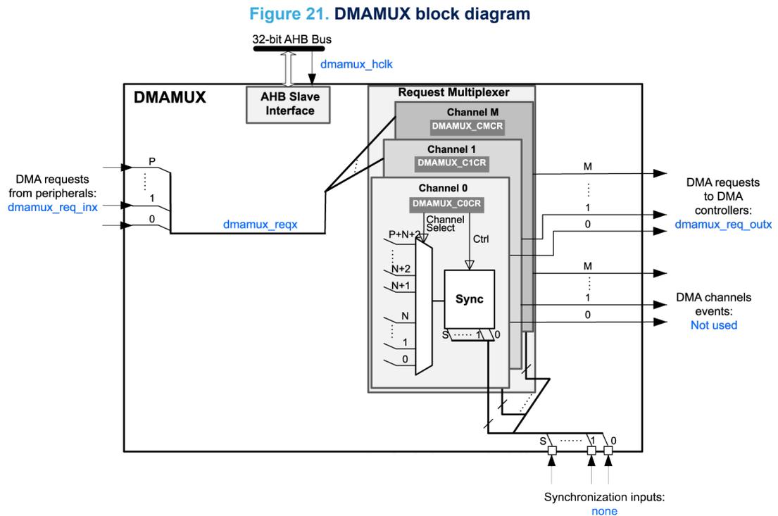
Figure 21. DMAMUX block diagram
The diagram illustrates the internal structure of the DMAMUX block. On the left, DMA requests from peripherals (labeled dmamux_req_inx ) enter through a multiplexer (inputs P, 1, 0). The output of this multiplexer is labeled dmamux_reqx . This signal enters the 'Request Multiplexer' block, which contains multiple channels (Channel 0, Channel 1, ..., Channel M). Each channel has its own control register (e.g., DMAMUX_C0CR, DMAMUX_C1CR, DMAMUX_CMCR). Inside each channel, there is a 'Channel Select' multiplexer (inputs P+N+2, N+2, N+1, N, ..., 1, 0) and a 'Sync' block. The outputs of the channels are labeled dmamux_req_outx and are connected to DMA controllers. Below the channels, there is a 'Sync' block with inputs S, ..., 1, 0, which are connected to synchronization inputs (labeled none ). The entire DMAMUX block is connected to a 32-bit AHB Bus via an 'AHB Slave Interface'. The interface has a signal labeled dmamux_hclk .
The implementation assigns:
- • DMAMUX request multiplexer sub-block inputs ( dmamux_reqx ) from peripherals ( dmamux_req_inx )
- • DMAMUX requests outputs to channels of DMA controllers (dmamux_req_outx)
11.4.2 DMAMUX channels
A DMAMUX channel is a DMAMUX request multiplexer channel which may include, depending on the selected input of the request multiplexer.
A DMAMUX request multiplexer channel is connected and dedicated to one single DMA controller(s) channel.
Channel configuration procedure
The following sequence should be followed to configure both a DMAMUX x channel and the related DMA channel y:
- 1. Set and configure completely the DMA channel y, except enabling the channel y.
- 2. Set and configure completely the related DMAMUX y channel.
- 3. Activate the DMA channel y by setting the EN bit in the DMA y channel register.
11.4.3 DMAMUX request line multiplexer
The DMAMUX request multiplexer with its multiple channels ensures the actual routing of DMA request/acknowledge control signals, named as DMA request lines.
Each DMA request line is connected in parallel to all the channels of the DMAMUX request line multiplexer.
A DMA request is sourced from the peripherals.
The DMAMUX request line multiplexer channel x selects the DMA request line number as configured by the 8-bit DMAREQ_ID field in the DMAMUX_CxCR register.
Note: The null value in the field DMAREQ_ID corresponds to no DMA request line selected. A same non-null DMA_REQ_ID value shall not be programmed to different x and y DMAMUX request multiplexer channels (via DMAMUX1_CxCR and DMAMUX CyCR). It is not allowed to configure a same non-null DMAREQ_ID to two different channels of the DMAMUX request line multiplexer.
On top of the DMA request selection, the synchronization mode and/or the event generation may be configured and enabled, if required.
11.5 DMAMUX registers
Refer to the table about register boundary addresses for the DMAMUX base address. The registers can only be accessed by words (32-bits).
11.5.1 DMAMUX request line multiplexer channel x configuration register (DMAMUX_CxCR)
Address offset: 0x04 * x (x = 0 to 7)
Reset value: 0x0000 0000
| 31 | 30 | 29 | 28 | 27 | 26 | 25 | 24 | 23 | 22 | 21 | 20 | 19 | 18 | 17 | 16 |
| RESERVED | |||||||||||||||
| 15 | 14 | 13 | 12 | 11 | 10 | 9 | 8 | 7 | 6 | 5 | 4 | 3 | 2 | 1 | 0 |
| RESERVED | DMAREQ_ID[4:0] | ||||||||||||||
| rw | |||||||||||||||
| Bits 31:5 | Reserved, must be kept at reset value. |
| Bits 4:0 | DMAREQ_ID[4:0]:
DMA request identification. Selects the input DMA request. DMAMUX table about assignments of multiplexer inputs to resources. |
11.5.2 DMAMUX register map
The following table summarizes the DMAMUX registers and reset values. Refer to the register boundary address table for the DMAMUX register base address.
Table 30. DMAMUX register map and reset values
| Offset | Register | 31 | 30 | 29 | 28 | 27 | 26 | 25 | 24 | 23 | 22 | 21 | 20 | 19 | 18 | 17 | 16 | 15 | 14 | 13 | 12 | 11 | 10 | 9 | 8 | 7 | 6 | 5 | 4 | 3 | 2 | 1 | 0 | |
|---|---|---|---|---|---|---|---|---|---|---|---|---|---|---|---|---|---|---|---|---|---|---|---|---|---|---|---|---|---|---|---|---|---|---|
| 0x000 | DMAMUX_C0CR | Res. | Res. | Res. | Res. | Res. | Res. | Res. | Res. | Res. | Res. | Res. | Res. | Res. | Res. | Res. | Res. | Res. | Res. | Res. | Res. | Res. | Res. | Res. | Res. | Res. | Res. | Res. | Res. | DMAREQ_ID[4:0] | ||||
| Reset value | 0 | 0 | 0 | 0 | 0 | |||||||||||||||||||||||||||||
| 0x004 | DMAMUX_C1CR | Res. | Res. | Res. | Res. | Res. | Res. | Res. | Res. | Res. | Res. | Res. | Res. | Res. | Res. | Res. | Res. | Res. | Res. | Res. | Res. | Res. | Res. | Res. | Res. | Res. | Res. | Res. | Res. | DMAREQ_ID[4:0] | ||||
| Reset value | 0 | 0 | 0 | 0 | 0 | |||||||||||||||||||||||||||||
| 0x008 | DMAMUX_C2CR | Res. | Res. | Res. | Res. | Res. | Res. | Res. | Res. | Res. | Res. | Res. | Res. | Res. | Res. | Res. | Res. | Res. | Res. | Res. | Res. | Res. | Res. | Res. | Res. | Res. | Res. | Res. | Res. | DMAREQ_ID[4:0] | ||||
| Reset value | 0 | 0 | 0 | 0 | 0 | |||||||||||||||||||||||||||||
| 0x00C | DMAMUX_C3CR | Res. | Res. | Res. | Res. | Res. | Res. | Res. | Res. | Res. | Res. | Res. | Res. | Res. | Res. | Res. | Res. | Res. | Res. | Res. | Res. | Res. | Res. | Res. | Res. | Res. | Res. | Res. | Res. | DMAREQ_ID[4:0] | ||||
| Reset value | 0 | 0 | 0 | 0 | 0 | |||||||||||||||||||||||||||||
| 0x010 | DMAMUX_C4CR | Res. | Res. | Res. | Res. | Res. | Res. | Res. | Res. | Res. | Res. | Res. | Res. | Res. | Res. | Res. | Res. | Res. | Res. | Res. | Res. | Res. | Res. | Res. | Res. | Res. | Res. | Res. | Res. | DMAREQ_ID[4:0] | ||||

| Offset | Register | 31 | 30 | 29 | 28 | 27 | 26 | 25 | 24 | 23 | 22 | 21 | 20 | 19 | 18 | 17 | 16 | 15 | 14 | 13 | 12 | 11 | 10 | 9 | 8 | 7 | 6 | 5 | 4 | 3 | 2 | 1 | 0 |
|---|---|---|---|---|---|---|---|---|---|---|---|---|---|---|---|---|---|---|---|---|---|---|---|---|---|---|---|---|---|---|---|---|---|
| 0x010 | Reset value | 0 | 0 | 0 | 0 | 0 | |||||||||||||||||||||||||||
| 0x014 | DMAMUX_C5CR | Res. | Res. | Res. | Res. | Res. | Res. | Res. | Res. | Res. | Res. | Res. | Res. | Res. | Res. | Res. | Res. | Res. | Res. | Res. | Res. | Res. | Res. | Res. | Res. | Res. | Res. | Res. | DMAREQ_ID[4:0] | ||||
| Reset value | 0 | 0 | 0 | 0 | 0 | ||||||||||||||||||||||||||||
| 0x018 | DMAMUX_C6CR | Res. | Res. | Res. | Res. | Res. | Res. | Res. | Res. | Res. | Res. | Res. | Res. | Res. | Res. | Res. | Res. | Res. | Res. | Res. | Res. | Res. | Res. | Res. | Res. | Res. | Res. | Res. | DMAREQ_ID[4:0] | ||||
| Reset value | 0 | 0 | 0 | 0 | 0 | ||||||||||||||||||||||||||||
| 0x01C | DMAMUX_C7CR | Res. | Res. | Res. | Res. | Res. | Res. | Res. | Res. | Res. | Res. | Res. | Res. | Res. | Res. | Res. | Res. | Res. | Res. | Res. | Res. | Res. | Res. | Res. | Res. | Res. | Res. | Res. | DMAREQ_ID[4:0] | ||||
| Reset value | 0 | 0 | 0 | 0 | 0 | ||||||||||||||||||||||||||||
| 0x020 0x3E8 | Reserved | Res. | |||||||||||||||||||||||||||||||