7. General-purpose I/O (GPIO)
7.1 Introduction
Each general-purpose I/O port has four 32-bit configuration registers (GPIOx_MODER, GPIOx_OTYPER, GPIOx_OSPEEDR and GPIOx_PUPDR), two 32-bit data registers (GPIOx_IDR and GPIOx_ODR) and a 32-bit set/reset register (GPIOx_BSRR). In addition all GPIOs have a 32-bit locking register (GPIOx_LCKR) and two 32-bit alternate function selection registers (GPIOx_AFRH and GPIOx_AFRL).
7.2 GPIO main features
- • Output states: push-pull or open drain +pull-up/down
- • Output data from output data register (GPIOx_ODR) or peripheral (alternate function output)
- • Speed selection for each I/O
- • Input states: floating, pull-up/down, analog
- • Input data to input data register (GPIOx_IDR) or peripheral (alternate function input)
- • Bit set and reset register (GPIOx_BSRR) for bitwise write access to GPIOx_ODR
- • Locking mechanism (GPIOx_LCKR) provided to freeze the I/O port configurations
- • Analog function
- • Alternate function selection registers
- • Fast toggle capable of changing every clock cycle
- • Highly flexible pin multiplexing allows the use of I/O pins as GPIOs or as one of several peripheral functions
7.3 GPIO functional description
Subject to the specific hardware characteristics of each I/O port listed in Section 4: I/O operating modes , each port bit of the general-purpose I/O (GPIO) ports can be individually configured by software in several modes:
- • Input floating
- • Input pull-up
- • Input pull-down
- • Analog
- • Output open-drain with pull-up or pull-down capability
- • Output push-pull with pull-up or pull-down capability
- • Alternate function push-pull with pull-up or pull-down capability
- • Alternate function open-drain with pull-up or pull-down capability
Each I/O port bit is freely programmable, however the I/O port registers have to be accessed as 32-bit words, half-words or bytes. The purpose of the GPIOx_BSRR and GPIOx_BRR registers is to allow atomic read/modify accesses to any of the GPIOx_ODR registers. In this way, there is no risk of an IRQ occurring between the read and the modify access.
Note: Open-drain and analog features are not available on all the I/Os of the STM32WB05xZ. Refer to Table 7. GPIO alternate options AF0, AF1 and AF2 modes and Table 8. GPIOs AF3, AF4 and AF6 modes footnotes .
Figure 15. Basic structure of a mixed analog/digital five-volt tolerant I/O port bit and Figure 16. Basic structure of a digital only five-volt tolerant I/O port bit show the basic structures of a mixed analog/digital 5 V tolerant I/O port bit and a digital only 5 V tolerant, respectively. Table 17. Port bit configuration gives the possible port bit configurations.
Figure 15. Basic structure of a mixed analog/digital five-volt tolerant I/O port bit
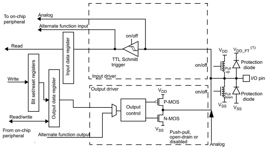
1. \( V_{DD\_FT} \) is a potential specific to five-volt tolerant I/Os and different from \( V_{DD} \) .
Figure 16. Basic structure of a digital only five-volt tolerant I/O port bit
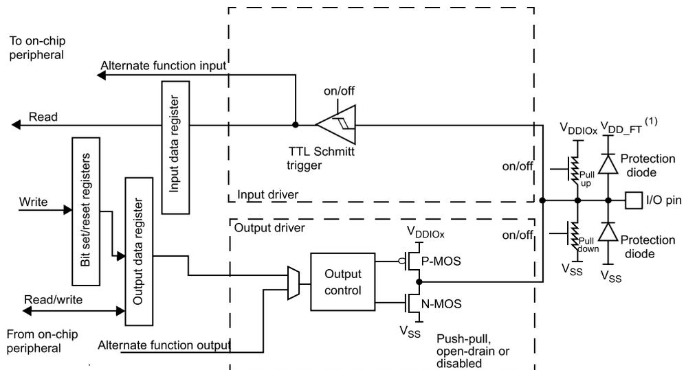
1. \( V_{DD\_FT} \) is a potential specific to five-volt tolerant I/Os and different from \( V_{DD} \) .
Table 17. Port bit configuration
| MODE(i) [1:0] | OTYPER(i) | OSPEED(i) [1:0] | PUPD(i) [1:0] | I/O configuration | |||
|---|---|---|---|---|---|---|---|
| 01 | 0 | SPEED [1:0] | 0 | 0 | GP output | PP | |
| 0 | 0 | 1 | GP output | PP + PU | |||
| 0 | 1 | 0 | GP output | PP + PD | |||
| 0 | 1 | 1 | Reserved | ||||
| 1 | 0 | 0 | GP output | OD | |||
| 1 | 0 | 1 | GP output | OD + PU | |||
| 1 | 1 | 0 | GP output | OD + PD | |||
| 1 | 1 | 1 | Reserved (GP output OD) | ||||
| 10 | 0 | SPEED [1:0] | 0 | 0 | AF | PP | |
| 0 | 0 | 1 | AF | PP + PU | |||
| 0 | 1 | 0 | AF | PP + PD | |||
| 0 | 1 | 1 | Reserved | ||||
| 1 | 0 | 0 | AF | OD | |||
| 1 | 0 | 1 | AF | OD + PU | |||
| 1 | 1 | 0 | AF | OD + PD | |||
| 1 | 1 | 1 | Reserved | ||||
| 00 | x | x | x | 0 | 0 | Input | Floating |
| x | x | x | 0 | 1 | Input | PU | |
| x | x | x | 1 | 0 | Input | PD | |
| x | x | x | 1 | 1 | Reserved (input floating) | ||
| 11 | x | x | x | 0 | 0 | Input/output | Analog |
| x | x | x | 0 | 1 | Reserved | ||
| x | x | x | 1 | 0 | |||
| x | x | x | 1 | 1 | |||
Note: GP = general-purpose, PP = push-pull, PU = pull-up, PD = pull-down, OD = open-drain, AF = alternate function.
Note: Open-drain and analog features are not available on all the I/Os of the STM32WB05xZ. Refer to Table 7. GPIO alternate options AF0, AF1 and AF2 modes and Table 8. GPIOs AF3, AF4 and AF6 modes .
7.3.1 General-purpose I/O (GPIO)
During and just after reset, the alternate functions are not active and most of the I/O ports are configured in GPIO input pull-up mode except the SWD debug pins. The debug pins are in AF0 pull-up/pull-down after reset:
- • PA2: DEBUG_SWDIO in pull-up
- • PA3: DEBUG_SWCLK in pull-down
When the pin is configured as output, the value written to the output data register (GPIOx_ODR) is output on the I/O pin. It is possible to use the output driver in push-pull mode or open-drain mode (only the low level is driven, high level is HI-Z).
The input data register (GPIOx_IDR) captures the data present on the I/O pin at every AHB clock cycle.
All GPIO pins have weak internal pull-up and pull-down resistors, which can be activated or not depending on the value in the GPIOx_PUPDR register.
7.3.2 I/O pin alternate function multiplexer and mapping
The device I/O pins are connected to on-board peripherals/modules through a multiplexer that allows only one peripheral alternate function (AF) connected to an I/O pin at a time. In this way, there can be no conflict between peripherals available on the same I/O pin.
Each I/O pin has a multiplexer with up to six alternate function inputs (AF0, AF1, AF2, AF3, AF4, AF6) that can be configured through the GPIOx_AFRRL (for pin 0 to 6) and GPIOx_AFRH (for pin 8 to 15) registers:
- • After reset the multiplexer selection is alternate function 0 (AF0). The I/Os are configured in alternate function mode through GPIOx_MODER register.
- • The specific alternate function assignments for each pin are detailed in .
In addition to this flexible I/O multiplexing architecture, each peripheral has alternate functions mapped onto different I/O pins to optimize the number of peripherals available in smaller packages.
To use an I/O in a given configuration, the user has to proceed as follows:
- • Debug function: after each device reset these pins are assigned as alternate function pins immediately usable by the debugger host
- • System function: RCC_MCO and RCC_LCO pins have to be configured in alternate function mode
- • GPIO: configures the desired I/O as output, input or analog in the GPIOx_MODER register
- •
Alternate function:
- – Connect the I/O to the desired AFx in one of the GPIOx_AFRRL or GPIOx_AFRH registers.
- – Select the type, pull-up/pull-down and output speed via GPIOx_OTYPER, GPIOx_PUPDR and GPIOx_OSPEEDER registers, respectively.
- – Configure the desired I/O as an alternate function in the GPIOx_MODER register.
- – Cortex-M0+ alternate function (EVENTOUT): The Cortex ® -M0+ output EVENTOUT signal can be output as alternate function on several I/Os. An event can be signaled through the configured pin after executing an SEV instruction.
- •
Additional functions:
- – For the ADC, configure the desired I/O in analog mode in GPIOx_MODER register and configure the required function in the ADC registers
Note: When configuring IOs in analog mode, the user must disable the pull-up/pull-down through the PWRC registers, if PWRC_CR1.APC is set.
Note: If PWRC_CR1.APC is set (default configuration), the pull-up/-down of the IOs is controlled by the PWRC_PUCRx and PWRC_PDCRx registers of the PWRC block. Otherwise it is controlled by the GPIOx_PUPDR register of the GPIO block.
- – For the additional functions such as Wakeup I/Os and LSE oscillator, configure the required function in the related PWRC, RCC, and RTC registers. These functions have priority over the configuration in the standard GPIO registers.
Refer to Table 10. I/O additional function mapping for the detailed mapping of the alternate function I/O pins.
7.3.3 I/O port control registers
Each of the GPIO ports has four 32-bit memory-mapped control registers (GPIOx_MODER, GPIOx_OTYPER, GPIOx_OSPEEDER, GPIOx_PUPDR) to configure up to 16 I/Os. The GPIOx_MODER register is used to select the I/O mode (input, output, AF, analog). The GPIOx_OTYPER and GPIOx_OSPEEDER registers are used to select the output type (push-pull or open-drain) and speed. The GPIOx_PUPDR register is used to select the pull-up/pull-down whatever the I/O direction.
7.3.4 I/O port data registers
Each GPIO has two 16-bit memory-mapped data registers: input and output data registers (GPIOx_IDR and GPIOx_ODR). GPIOx_ODR stores the data to be output, it is read/write accessible. The data input through the I/O are stored into the input data register (GPIOx_IDR), a read-only register. See Section 7.4.9: GPIOA port input data register (GPIOA_IDR) and Section 7.4.11: GPIOA port output data register (GPIOA_ODR) .
7.3.5 I/O data bitwise handling
The bit set reset register (GPIOx_BSRR) is a 32-bit register, which allows the application to set and reset each individual bit in the output data register (GPIOx_ODR). The bit set reset register has twice the size of GPIOx_ODR.
To each bit in GPIOx_ODR, two control bits in GPIOx_BSRR: BS(i) and BR(i) correspond. When written to 1, bit BS(i) sets the corresponding ODR(i) bit. When written to 1, bit BR(i) resets the ODR(i) corresponding bit.
Writing any bit to 0 in GPIOx_BSRR does not have any effect on the corresponding bit in GPIOx_ODR. If there is an attempt to both set and reset a bit in GPIOx_BSRR, the set action takes priority.
Using the GPIOx_BSRR register to change the values of individual bits in GPIOx_ODR is a “one-shot” effect that does not lock the GPIOx_ODR bits. The GPIOx_ODR bits can always be accessed directly. The GPIOx_BSRR register provides a way of performing atomic bitwise handling.
There is no need for the software to disable interrupts when programming the GPIOx_ODR at bit level: it is possible to modify one or more bits in a single atomic AHB write access.
7.3.6 GPIO locking mechanism
It is possible to freeze the GPIO control registers by applying a specific write sequence to the GPIOx_LCKR register. The frozen registers are GPIOx_MODER, GPIOx_OTYPER, GPIOx_OSPEEDR, GPIOx_PUPDR, GPIOx_AFR and GPIOx_AFRH.
To write the GPIOx_LCKR register, a specific write / read sequence has to be applied. When the right LOCK sequence is applied to bit 16 in this register, the value of LCKR[15:0] is used to lock the configuration of the I/Os (during the write sequence the LCKR[15:0] value must be the same). When the LOCK sequence has been applied to a port bit, the value of the port bit can no longer be modified until the next MCU reset or peripheral reset. Each GPIOx_LCKR bit freezes the corresponding bit in the control registers (GPIOx_MODER, GPIOx_OTYPER, GPIOx_OSPEEDR, GPIOx_PUPDR, GPIOx_AFR and GPIOx_AFRH).
The LOCK sequence (refer to GPIO port bit set/register (GPIOxB_BSRR)) can only be performed using a word (32-bit long) access to the GPIOx_LCKR register due to the fact that GPIOx_LCKR bit 16 has to be set at the same time as the [15:0] bits.
For more details refer to the LCKR register description in GPIO port bit set/register (GPIOxB_BSRR).
7.3.7 I/O alternate function input/output
Two registers are provided to select one of the alternate function inputs/outputs available for each I/O. With these registers, the users can connect an alternate function to some other pin as required by their application.
This means that a number of possible peripheral functions are multiplexed on each GPIO using the GPIOx_AFR and GPIOx_AFRH alternate function registers. The application can thus select any one of the possible functions for each I/O. The AF selection signal being common to the alternate function input and alternate function output, a single channel is selected for the alternate function input/output of a given I/O.
To know which functions are multiplexed on each GPIO pin, refer to Section 4: I/O operating modes .
7.3.8 External interrupt/wakeup lines
All ports have external interrupt capability. To use external interrupt lines, the IO port must be configured in input mode. The interruption configuration (level/edge, polarity, mask) has to be done in the system controller (SYSCFG). See Section 8: System controller (SYSCFG) .
7.3.9 Input configuration
When the I/O port is programmed as input:
- • The output buffer is disabled
- • The Schmitt trigger input is activated
- • The pull-up and pull-down resistors are activated depending on the value in the GPIOx_PUPDR register
- • The data present on the I/O pin are sampled into the input data register every AHB clock cycle
- • A read access to the input data register provides the I/O state.
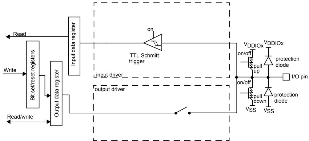
Figure 17. Input floating/pull-up/pull-down configurations shows the input configuration of the I/O port bit.
Figure 17. Input floating/pull-up/pull-down configurations
7.3.10
Output configuration
When the I/O port is programmed as output:
- • The output buffer is enabled:
- – Open drain mode: A “0” in the Output register activates the N-MOS whereas a “1” in the Output register leaves the port in Hi-Z (the P-MOS is never activated)
- – Push-pull mode: A “0” in the Output register activates the N-MOS whereas a “1” in the Output register activates the P-MOS
- • The Schmitt trigger input is activated
- • The pull-up and pull-down resistors are activated depending on the value in the GPIOx_PUPDR register
- • The data present on the I/O pin are sampled into the input data register every AHB clock cycle
- • A read access to the input data register gets the I/Ostate
- • A read access to the output data register gets the last written value
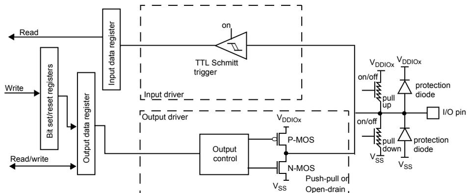
Figure 18. Output configuration shows the output configuration of the I/O port bit.
Figure 18. Output configuration
7.3.11 Alternate function configuration
When the I/O port is programmed as alternate function:
- • The output buffer can be configured in open-drain or push-pull mode
- • The output buffer is driven by the signals coming from the peripheral (transmitter enable and data)
- • The Schmitt trigger input is activated
- • The weak pull-up and pull-down resistors are activated or not depending on the value in the GPIOx_PUPDR register
- • The data present on the I/O pin are sampled into the input data register every AHB clock cycle
- • A read access to the input data register gets the I/O state.
Figure 19. Alternate function configuration shows the alternate function configuration of the I/O port bit.
Figure 19. Alternate function configuration
7.3.12 Analog configuration
When the I/O port is programmed as analog configuration:
- • The output buffer is disabled
- • The Schmitt trigger input is deactivated, providing zero consumption for every analog value of the I/O pin. The output of the Schmitt trigger is forced to a constant value (0).
- • The pull-up and pull-down resistors have to be disabled by the software or else the associated analog feature does not work as expected.
- • Read access to the input data register gets the value "0".
Figure 20. High impedance-analog configuration shows the high-impedance, analog-input configuration of the I/O port bit.
Figure 20. High impedance-analog configuration
7.3.13 Using the LSE oscillator pins as GPIOs
When the LSE oscillator is switched OFF (default state after reset), the related oscillator pins can be used as normal GPIOs.
When the oscillator is configured in user external clock mode, only the RCC_OSC32_IN pin is reserved for clock input and the RCC_OSC32_OUT pin can still be used as normal GPIO.
Note: The high speed oscillator (HSE) OSC_IN and OSC_OUT pins are dedicated oscillator pins and can not be used as GPIO.
7.4 GPIO registers
This section gives a detailed description of the GPIO registers.
For a summary of register bits, register address offsets and reset values, refer to Table 18. GPIO register map and reset values . The peripheral registers can be written in word, half word or byte mode.
7.4.1 GPIOA port mode register (GPIOA_MODER)
Address offset: 0x00
Reset values:
- 0x0000 00A0
| 31 | 30 | 29 | 28 | 27 | 26 | 25 | 24 | 23 | 22 | 21 | 20 | 19 | 18 | 17 | 16 |
|---|---|---|---|---|---|---|---|---|---|---|---|---|---|---|---|
| Res. | Res. | Res. | Res. | Res. | Res. | Res. | Res. | MODE11[1:0] | MODE10[1:0] | MODE9[1:0] | MODE8[1:0] | ||||
| rw | rw | rw | rw | rw | rw | rw | rw | ||||||||
| 15 | 14 | 13 | 12 | 11 | 10 | 9 | 8 | 7 | 6 | 5 | 4 | 3 | 2 | 1 | 0 |
| Res. | Res. | Res. | Res. | Res. | Res. | Res. | Res. | MODE3[1:0] | MODE2[1:0] | MODE1[1:0] | MODE0[1:0] | ||||
| rw | rw | rw | rw | rw | rw | rw | rw | ||||||||
| Bits 2y+1:2y | MODEy[1:0]: Port A configuration bits (y = 0..15). These bits are written by software to configure the I/O mode. 00: Input mode 01: General purpose output mode 10: Alternate function mode 11: Analog mode Note: When configuring a pad in analog mode, the user must take care to disable the associated pull-up/down to avoid pollution on the analog signal. |
7.4.2 GPIOB port mode register (GPIOB_MODER)
Address offset: 0x00
Reset values:
- 0x0000 0000
| 31 | 30 | 29 | 28 | 27 | 26 | 25 | 24 | 23 | 22 | 21 | 20 | 19 | 18 | 17 | 16 |
|---|---|---|---|---|---|---|---|---|---|---|---|---|---|---|---|
| MODE15[1:0] | MODE14[1:0] | MODE13[1:0] | MODE12[1:0] | Res. | Res. | Res. | Res. | Res. | Res. | Res. | Res. | ||||
| rw | rw | rw | rw | rw | rw | rw | rw | ||||||||
| 15 | 14 | 13 | 12 | 11 | 10 | 9 | 8 | 7 | 6 | 5 | 4 | 3 | 2 | 1 | 0 |
| MODE7[1:0] | MODE6[1:0] | MODE5[1:0] | MODE4[1:0] | MODE3[1:0] | MODE2[1:0] | MODE1[1:0] | MODE0[1:0] | ||||||||
| rw | rw | rw | rw | rw | rw | rw | rw | rw | rw | rw | rw | rw | rw | rw | rw |
| Bits 2y+1:2y | MODEy[1:0]: Port B configuration bits (y = 0..15). These bits are written by software to configure the I/O mode. 00: Input mode 01: General purpose output mode 10: Alternate function mode 11: Analog mode Note: When configuring a pad in analog mode, the user must take care to disable the associated pull-up/down to avoid pollution on the analog signal. |
7.4.3 GPIOA port output type register (GPIOA_OTYPER)
Address offset: 0x04
Reset value: 0x0000 0000
| 31 | 30 | 29 | 28 | 27 | 26 | 25 | 24 | 23 | 22 | 21 | 20 | 19 | 18 | 17 | 16 |
|---|---|---|---|---|---|---|---|---|---|---|---|---|---|---|---|
| Res. | Res. | Res. | Res. | Res. | Res. | Res. | Res. | Res. | Res. | Res. | Res. | Res. | Res. | Res. | Res. |
| 15 | 14 | 13 | 12 | 11 | 10 | 9 | 8 | 7 | 6 | 5 | 4 | 3 | 2 | 1 | 0 |
| Res. | Res. | Res. | Res. | OT11 | OT10 | OT9 | OT8 | Res. | Res. | Res. | Res. | OT3 | OT2 | OT1 | OT0 |
| rw | rw | rw | rw | rw | rw | rw | rw |
| Bits 31:16 | Reserved, must be kept at reset value. |
| Bits 15:0 | OTy:
Port A configuration bits (y = 0..15). These bits are written by software to configure the I/O output type. 0: Output push-pull (reset state) 1: Output open-drain |
7.4.4 GPIOB port output type register (GPIOB_OTYPER)
Address offset: 0x04
Reset value: 0x0000 0000
| 31 | 30 | 29 | 28 | 27 | 26 | 25 | 24 | 23 | 22 | 21 | 20 | 19 | 18 | 17 | 16 |
|---|---|---|---|---|---|---|---|---|---|---|---|---|---|---|---|
| Res. | Res. | Res. | Res. | Res. | Res. | Res. | Res. | Res. | Res. | Res. | Res. | Res. | Res. | Res. | Res. |
| 15 | 14 | 13 | 12 | 11 | 10 | 9 | 8 | 7 | 6 | 5 | 4 | 3 | 2 | 1 | 0 |
| OT15 | OT14 | OT13 | OT12 | Res. | Res. | Res. | Res. | OT7 | OT6 | OT5 | OT4 | OT3 | OT2 | OT1 | OT0 |
| rw | rw | rw | rw | rw | rw | rw | rw | rw | rw | rw | rw |
| Bits 31:16 | Reserved, must be kept at reset value. |
| Bits 15:0 | OTy:
Port B configuration bits (y = 0..15). These bits are written by software to configure the I/O output type. 0: Output push-pull (reset state) 1: Output open-drain |
7.4.5 GPIOA port output speed register (GPIOA_OSPEEDR)
Address offset: 0x08
Reset values:
- 0x0000 0030
| 31 | 30 | 29 | 28 | 27 | 26 | 25 | 24 | 23 | 22 | 21 | 20 | 19 | 18 | 17 | 16 |
|---|---|---|---|---|---|---|---|---|---|---|---|---|---|---|---|
| Res. | Res. | Res. | Res. | Res. | Res. | Res. | Res. | OSPEED11 [1:0] | OSPEED10 [1:0] | OSPEED9 [1:0] | OSPEED8 [1:0] | ||||
| rw | rw | rw | rw | rw | rw | rw | rw | ||||||||
| 15 | 14 | 13 | 12 | 11 | 10 | 9 | 8 | 7 | 6 | 5 | 4 | 3 | 2 | 1 | 0 |
| Res. | Res. | Res. | Res. | Res. | Res. | Res. | Res. | OSPEED3 [1:0] | OSPEED2 [1:0] | OSPEED1 [1:0] | OSPEED0 [1:0] | ||||
| rw | rw | rw | rw | rw | rw | rw | rw | ||||||||
| Bits 2y+1:2y | OSPEEDy[1:0]:
Port A configuration bits (y = 0..15). These bits are written by software to configure the I/O output speed. |
7.4.6 GPIOB port output speed register (GPIOB_OSPEEDR)
Address offset: 0x08
Reset values:
- 0x0000 0000
| 31 | 30 | 29 | 28 | 27 | 26 | 25 | 24 | 23 | 22 | 21 | 20 | 19 | 18 | 17 | 16 |
|---|---|---|---|---|---|---|---|---|---|---|---|---|---|---|---|
| OSPEED15 [1:0] | OSPEED14 [1:0] | OSPEED13 [1:0] | OSPEED12 [1:0] | Res. | Res. | Res. | Res. | Res. | Res. | Res. | Res. | ||||
| rw | rw | rw | rw | rw | rw | rw | rw | ||||||||
| 15 | 14 | 13 | 12 | 11 | 10 | 9 | 8 | 7 | 6 | 5 | 4 | 3 | 2 | 1 | 0 |
| OSPEED7 [1:0] | OSPEED6 [1:0] | OSPEED5 [1:0] | OSPEED4 [1:0] | OSPEED3 [1:0] | OSPEED2 [1:0] | OSPEED1 [1:0] | OSPEED0 [1:0] | ||||||||
| rw | rw | rw | rw | rw | rw | rw | rw | rw | rw | rw | rw | rw | rw | rw | rw |
| Bits 2y+1:2y | OSPEEDy[1:0]:
Port B configuration bits (y = 0..15). These bits are written by software to configure the I/O output speed. |
7.4.7 GPIOA port pull-up/pull-down register (GPIOA_PUPDR)
Address offset: 0x0C
Reset values:
- 0x0055 0095
| 31 | 30 | 29 | 28 | 27 | 26 | 25 | 24 | 23 | 22 | 21 | 20 | 19 | 18 | 17 | 16 |
|---|---|---|---|---|---|---|---|---|---|---|---|---|---|---|---|
| Res. | Res. | Res. | Res. | Res. | Res. | Res. | Res. | PUPD11[1:0] | PUPD10[1:0] | PUPD9[1:0] | PUPD8[1:0] | ||||
| rw | rw | rw | rw | rw | rw | rw | rw | ||||||||
| 15 | 14 | 13 | 12 | 11 | 10 | 9 | 8 | 7 | 6 | 5 | 4 | 3 | 2 | 1 | 0 |
| Res. | Res. | Res. | Res. | Res. | Res. | Res. | Res. | PUPD3[1:0] | PUPD2[1:0] | PUPD1[1:0] | PUPD0[1:0] | ||||
| rw | rw | rw | rw | rw | rw | rw | rw | ||||||||
| Bits 2y+1:2y | PUPDy[1:0]: Port A configuration bits (y = 0..15). These bits are written by software to configure the I/O pull-up or pull-down. 00: No pull-up, pull-down 01: Pull-up 10: Pull-down 11: Reserved |
Note: When PWRC_CR1[4] = APC bit is set, GPIOA_PUPDR has no effect on the behavior. When PWRC_CR1[4] = APC bit is not set, GPIOA_PUPDR pull configuration is not effective under low power modes.
7.4.8 GPIOB port pull-up/pull-down register (GPIOB_PUPDR)
Address offset: 0x0C Reset values:
- 0x0055 5555
| 31 | 30 | 29 | 28 | 27 | 26 | 25 | 24 | 23 | 22 | 21 | 20 | 19 | 18 | 17 | 16 |
|---|---|---|---|---|---|---|---|---|---|---|---|---|---|---|---|
| PUPD15[1:0] | PUPD14[1:0] | PUPD13[1:0] | PUPD12[1:0] | Res. | Res. | Res. | Res. | Res. | Res. | Res. | Res. | ||||
| rw | rw | rw | rw | rw | rw | rw | rw | ||||||||
| 15 | 14 | 13 | 12 | 11 | 10 | 9 | 8 | 7 | 6 | 5 | 4 | 3 | 2 | 1 | 0 |
| PUPD7[1:0] | PUPD6[1:0] | PUPD5[1:0] | PUPD4[1:0] | PUPD3[1:0] | PUPD2[1:0] | PUPD1[1:0] | PUPD0[1:0] | ||||||||
| rw | rw | rw | rw | rw | rw | rw | rw | rw | rw | rw | rw | rw | rw | rw | rw |
| Bits 2y+1:2y | PUPDy[1:0]: Port B configuration bits (y = 0..15). These bits are written by software to configure the I/O pull-up or pull-down. 00: No pull-up, pull-down 01: Pull-up 10: Pull-down 11: Reserved |
Note: When PWRC_CR1[4] = APC bit is set, GPIOB_PUPDR has no effect on the behavior. When PWRC_CR1[4] = APC bit is not set, GPIOB_PUPDR pull configuration is not effective under low power modes.
7.4.9 GPIOA port input data register (GPIOA_IDR)
Address offset: 0x10
Reset value: 0x0000 XXXX (where X means undefined)
| 31 | 30 | 29 | 28 | 27 | 26 | 25 | 24 | 23 | 22 | 21 | 20 | 19 | 18 | 17 | 16 |
|---|---|---|---|---|---|---|---|---|---|---|---|---|---|---|---|
| Res. | Res. | Res. | Res. | Res. | Res. | Res. | Res. | Res. | Res. | Res. | Res. | Res. | Res. | Res. | Res. |
| 15 | 14 | 13 | 12 | 11 | 10 | 9 | 8 | 7 | 6 | 5 | 4 | 3 | 2 | 1 | 0 |
| Res. | Res. | Res. | ID12 | ID11 | ID10 | ID9 | ID8 | Res. | Res. | Res. | Res. | ID3 | ID2 | ID1 | ID0 |
| r | r | r | r | r | r | r | r | r |
| Bits 31:16 | Reserved, must be kept at reset value. |
| Bits 15:0 | IDy:
Port A input data bit (y = 0..15). These bits are read-only. They contain the input value of the corresponding I/O port. |
7.4.10 GPIOB port input data register (GPIOB_IDR)
Address offset: 0x10
Reset value: 0x0000 XXXX (where X means undefined)
| 31 | 30 | 29 | 28 | 27 | 26 | 25 | 24 | 23 | 22 | 21 | 20 | 19 | 18 | 17 | 16 |
|---|---|---|---|---|---|---|---|---|---|---|---|---|---|---|---|
| Res. | Res. | Res. | Res. | Res. | Res. | Res. | Res. | Res. | Res. | Res. | Res. | Res. | Res. | Res. | Res. |
| 15 | 14 | 13 | 12 | 11 | 10 | 9 | 8 | 7 | 6 | 5 | 4 | 3 | 2 | 1 | 0 |
| ID15 | ID14 | ID13 | ID12 | Res. | Res. | Res. | Res. | ID7 | ID6 | ID5 | ID4 | ID3 | ID2 | ID1 | ID0 |
| r | r | r | r | r | r | r | r | r | r | r | r | r | r | r | r |
| Bits 31:16 | Reserved, must be kept at reset value. |
| Bits 15:0 | IDy:
Port B input data bit (y = 0..15). These bits are read-only. They contain the input value of the corresponding I/O port. |
7.4.11 GPIOA port output data register (GPIOA_ODR)
Address offset: 0x14
Reset value: 0x0000 0000
| 31 | 30 | 29 | 28 | 27 | 26 | 25 | 24 | 23 | 22 | 21 | 20 | 19 | 18 | 17 | 16 |
| Res. | Res. | Res. | Res. | Res. | Res. | Res. | Res. | Res. | Res. | Res. | Res. | Res. | Res. | Res. | Res. |
| 15 | 14 | 13 | 12 | 11 | 10 | 9 | 8 | 7 | 6 | 5 | 4 | 3 | 2 | 1 | 0 |
| Res. | Res. | Res. | Res. | OD11 | OD10 | OD9 | OD8 | Res. | Res. | Res. | Res. | OD3 | OD2 | OD1 | OD0 |
| rw | rw | rw | rw | rw | rw | rw | rw |
| Bits 31:16 | Reserved, must be kept at reset value. |
| Bits 15:0 | ODy:
Port A output data bit (y = 0..15). These bits can be read and written by software. Note: For atomic bit set/reset, the OD bits can be individually set and/or reset by writing to the GPIOx_BSRR or GPIOx_BRR registers (x = A, B). |
7.4.12 GPIOB port output data register (GPIOB_ODR)
Address offset: 0x14
Reset value: 0x0000 0000
| 31 | 30 | 29 | 28 | 27 | 26 | 25 | 24 | 23 | 22 | 21 | 20 | 19 | 18 | 17 | 16 |
| Res. | Res. | Res. | Res. | Res. | Res. | Res. | Res. | Res. | Res. | Res. | Res. | Res. | Res. | Res. | Res. |
| 15 | 14 | 13 | 12 | 11 | 10 | 9 | 8 | 7 | 6 | 5 | 4 | 3 | 2 | 1 | 0 |
| OD15 | OD14 | OD13 | OD12 | Res. | Res. | Res. | Res. | OD7 | OD6 | OD5 | OD4 | OD3 | OD2 | OD1 | OD0 |
| rw | rw | rw | rw | rw | rw | rw | rw | rw | rw | rw | rw |
| Bits 31:16 | Reserved, must be kept at reset value. |
| Bits 15:0 | ODy:
Port B output data bit (y = 0..15). These bits can be read and written by software. Note: For atomic bit set/reset, the OD bits can be individually set and/or reset by writing to the GPIOx_BSRR or GPIOx_BRR registers (x = A, B). |
7.4.13 GPIOA port bit set/reset register (GPIOA_BSRR)
Address offset: 0x18
Reset value: 0x0000 0000
| 31 | 30 | 29 | 28 | 27 | 26 | 25 | 24 | 23 | 22 | 21 | 20 | 19 | 18 | 17 | 16 |
|---|---|---|---|---|---|---|---|---|---|---|---|---|---|---|---|
| Res. | Res. | Res. | Res. | BR11 | BR10 | BR9 | BR8 | Res. | Res. | Res. | Res. | BR3 | BR2 | BR1 | BR0 |
| w | w | w | w | w | w | w | w | ||||||||
| 15 | 14 | 13 | 12 | 11 | 10 | 9 | 8 | 7 | 6 | 5 | 4 | 3 | 2 | 1 | 0 |
| Res. | Res. | Res. | Res. | BS11 | BS10 | BS9 | BS8 | Res. | Res. | Res. | Res. | BS3 | BS2 | BS1 | BS0 |
| w | w | w | w | w | w | w | w |
| Bits 31:16 | BRy: Port A reset bit y (y = 0..15). These bits are write-only. A read to these bits returns the value 0x0000. 0: No action on the corresponding ODx bit 1: Resets the corresponding ODx bit Note: If both BSx and BRx are set, BSx has priority. |
| Bits 15:0 | BSy: Port A set bit y (y= 0..15). These bits are write-only. A read to these bits returns the value 0x0000. 0: No action on the corresponding ODx bit 1: Set the corresponding ODx bit |
7.4.14 GPIOB port bit set/reset register (GPIOB_BSRR)
Address offset: 0x18
Reset value: 0x0000 0000
| 31 | 30 | 29 | 28 | 27 | 26 | 25 | 24 | 23 | 22 | 21 | 20 | 19 | 18 | 17 | 16 |
|---|---|---|---|---|---|---|---|---|---|---|---|---|---|---|---|
| BR15 | BR14 | BR13 | BR12 | Res. | Res. | Res. | Res. | BR7 | BR6 | BR5 | BR4 | BR3 | BR2 | BR1 | BR0 |
| w | w | w | w | w | w | w | w | w | w | w | w | ||||
| 15 | 14 | 13 | 12 | 11 | 10 | 9 | 8 | 7 | 6 | 5 | 4 | 3 | 2 | 1 | 0 |
| BS15 | BS14 | BS13 | BS12 | Res. | Res. | Res. | Res. | BS7 | BS6 | BS5 | BS4 | BS3 | BS2 | BS1 | BS0 |
| w | w | w | w | w | w | w | w | w | w | w | w |
| Bits 31:16 | BRy: Port B reset bit y (y = 0..15). These bits are write-only. A read to these bits returns the value 0x0000. 0: No action on the corresponding ODx bit 1: Resets the corresponding ODx bit Note: If both BSx and BRx are set, BSx has priority. |
| Bits 15:0 | BSy: Port B set bit y (y= 0..15). These bits are write-only. A read to these bits returns the value 0x0000. 0: No action on the corresponding ODx bit 1: Set the corresponding ODx bit |
7.4.15 GPIOA port configuration lock register (GPIOA_LCKR)
This register is used to lock the configuration of the port bits when a correct write sequence is applied to bit 16 (LCKK). The value of bits [15:0] is used to lock the configuration of the GPIO. During the write sequence, the value of LCKR[15:0] must not change. When the LOCK sequence has been applied on a port bit, the value of this port bit can no longer be modified until the next MCU reset or peripheral resets.
Note: A specific write sequence is used to write to the GPIOx_LCKR register. Only word access (32-bit long) is allowed during this locking sequence.
Each lock bit freezes a specific configuration register (control and alternate function registers).
Address offset: 0x1C
Reset value: 0x0000 0000
| 31 | 30 | 29 | 28 | 27 | 26 | 25 | 24 | 23 | 22 | 21 | 20 | 19 | 18 | 17 | 16 |
| Res. | Res. | Res. | Res. | Res. | Res. | Res. | Res. | Res. | Res. | Res. | Res. | Res. | Res. | Res. | LCKK |
| rw | |||||||||||||||
| 15 | 14 | 13 | 12 | 11 | 10 | 9 | 8 | 7 | 6 | 5 | 4 | 3 | 2 | 1 | 0 |
| Res. | Res. | Res. | Res. | LCK11 | LCK10 | LCK9 | LCK8 | Res. | Res. | Res. | Res. | LCK3 | LCK2 | LCK1 | LCK0 |
| rw | rw | rw | rw | rw | rw | rw | rw |
| Bits 31:17 | Reserved, must be kept at reset value. |
| Bit 16 | LCKK: Lock key. This bit can be read any time. It can only be modified using the lock key write sequence. 0: Port configuration lock key not active 0: Port configuration lock key not active 1: Port configuration lock key active. The GPIOx_LCKR register is locked until the next MCU reset or peripheral reset. LOCK key write sequence: WR LCKR[16] = '1' + LCKR[15:0] RD LCKR[16] = '1' (this read operation is optional but it confirms that the lock is active) Note: During the LOCK key write sequence, the value of LCK[15:0] must not change. Any error in the lock sequence aborts the lock. After the first lock sequence on any bit of the port, any read access on the LCKK bit returns '1' until the next MCU reset or peripheral reset. |
| Bits 15:0 | LCKy: Port A lock bit y (y= 0..15). These bits are read/write but can only be written when the LCKK bit is '0', using the specific sequence described in LCKK bit description. 0: Port configuration not locked |
7.4.16 GPIOB port configuration lock register (GPIOB_LCKR)
This register is used to lock the configuration of the port bits when a correct write sequence is applied to bit 16 (LCKK). The value of bits [15:0] is used to lock the configuration of the GPIO. During the write sequence, the value of LCKR[15:0] must not change. When the LOCK sequence has been applied on a port bit, the value of this port bit can no longer be modified until the next MCU reset or peripheral resets.
Note: A specific write sequence is used to write to the GPIOx_LCKR register. Only word access (32-bit long) is allowed during this locking sequence.
Each lock bit freezes a specific configuration register (control and alternate function registers).
Address offset: 0x1C
Reset value: 0x0000 0000
| 31 | 30 | 29 | 28 | 27 | 26 | 25 | 24 | 23 | 22 | 21 | 20 | 19 | 18 | 17 | 16 |
| Res. | Res. | Res. | Res. | Res. | Res. | Res. | Res. | Res. | Res. | Res. | Res. | Res. | Res. | Res. | LCKKK |
| rw | |||||||||||||||
| 15 | 14 | 13 | 12 | 11 | 10 | 9 | 8 | 7 | 6 | 5 | 4 | 3 | 2 | 1 | 0 |
| LCK15 | LCK14 | LCK13 | LCK12 | Res. | Res. | Res. | Res. | LCK7 | LCK6 | LCK5 | LCK4 | LCK3 | LCK2 | LCK1 | LCK0 |
| rw | rw | rw | rw | rw | rw | rw | rw | rw | rw | rw | rw |
| Bits 31:17 | Reserved, must be kept at reset value. |
| Bit 16 | LCKKK: Lock key. This bit can be read any time. It can only be modified using the lock key write sequence. 0: Port configuration lock key not active |
| Bits 15:0 | LCKy: Port B lock bit y (y= 0..15). These bits are read/write but can only be written when the LCKKK bit is '0', using the specific sequence described in LCKKK bit description. |
7.4.17 GPIOA alternate function low register (GPIOA_AFRL)
Address offset: 0x20
Reset value: 0x0000 0000
| 31 | 30 | 29 | 28 | 27 | 26 | 25 | 24 | 23 | 22 | 21 | 20 | 19 | 18 | 17 | 16 |
|---|---|---|---|---|---|---|---|---|---|---|---|---|---|---|---|
| Res. | Res. | Res. | Res. | Res. | Res. | Res. | Res. | Res. | Res. | Res. | Res. | Res. | Res. | Res. | Res. |
| 15 | 14 | 13 | 12 | 11 | 10 | 9 | 8 | 7 | 6 | 5 | 4 | 3 | 2 | 1 | 0 |
| AFSEL3[3:0] | AFSEL2[3:0] | AFSEL1[3:0] | AFSEL0[3:0] | ||||||||||||
| rw | rw | rw | rw | rw | rw | rw | rw | rw | rw | rw | rw | rw | rw | rw | rw |
| Bits 31:0 | y[3:0]:
Alternate function selection for port A pin y (y = 0..7). |
7.4.18 GPIOB alternate function low register (GPIOB_AFRL)
Address offset: 0x20
Reset value: 0x0000 0000
| 31 | 30 | 29 | 28 | 27 | 26 | 25 | 24 | 23 | 22 | 21 | 20 | 19 | 18 | 17 | 16 |
|---|---|---|---|---|---|---|---|---|---|---|---|---|---|---|---|
| AFSEL7[3:0] | AFSEL6[3:0] | AFSEL5[3:0] | AFSEL4[3:0] | ||||||||||||
| rw | rw | rw | rw | rw | rw | rw | rw | rw | rw | rw | rw | rw | rw | rw | rw |
| 15 | 14 | 13 | 12 | 11 | 10 | 9 | 8 | 7 | 6 | 5 | 4 | 3 | 2 | 1 | 0 |
| AFSEL3[3:0] | AFSEL2[3:0] | AFSEL1[3:0] | AFSEL0[3:0] | ||||||||||||
| rw | rw | rw | rw | rw | rw | rw | rw | rw | rw | rw | rw | rw | rw | rw | rw |
| Bits 31:0 | y[3:0]:
Alternate function selection for port B pin y (y = 0..7). |
7.4.19 GPIOA alternate function high register (GPIOA_AFRH)
Address offset: 0x24
Reset value: 0x0000 0000
| 31 | 30 | 29 | 28 | 27 | 26 | 25 | 24 | 23 | 22 | 21 | 20 | 19 | 18 | 17 | 16 |
|---|---|---|---|---|---|---|---|---|---|---|---|---|---|---|---|
| Res. | Res. | Res. | Res. | Res. | Res. | Res. | Res. | Res. | Res. | Res. | Res. | Res. | Res. | Res. | Res. |
| 15 | 14 | 13 | 12 | 11 | 10 | 9 | 8 | 7 | 6 | 5 | 4 | 3 | 2 | 1 | 0 |
| AFSEL11[3:0] | AFSEL10[3:0] | AFSEL9[3:0] | AFSEL8[3:0] | ||||||||||||
| rw | rw | rw | rw | rw | rw | rw | rw | rw | rw | rw | rw | rw | rw | rw | rw |
| Bits 31:0 | y[3:0]: Alternate function selection for port A pin y (y = 8..15). These bits are written by software to configure alternate function I/Os. AFSEL y selection:
|
7.4.20 GPIOB alternate function high register (GPIOB_AFRH)
Address offset: 0x24
Reset value: 0x0000 0000
| 31 | 30 | 29 | 28 | 27 | 26 | 25 | 24 | 23 | 22 | 21 | 20 | 19 | 18 | 17 | 16 |
|---|---|---|---|---|---|---|---|---|---|---|---|---|---|---|---|
| AFSEL15[3:0] | AFSEL14[3:0] | AFSEL13[3:0] | AFSEL12[3:0] | ||||||||||||
| rw | rw | rw | rw | rw | rw | rw | rw | rw | rw | rw | rw | rw | rw | rw | rw |
| 15 | 14 | 13 | 12 | 11 | 10 | 9 | 8 | 7 | 6 | 5 | 4 | 3 | 2 | 1 | 0 |
| Res. | Res. | Res. | Res. | Res. | Res. | Res. | Res. | Res. | Res. | Res. | Res. | Res. | Res. | Res. | Res. |
| rw | rw | rw | rw | rw | rw | rw | rw | rw | rw | rw | rw | rw | rw | rw | rw |
| Bits 31:0 | y[3:0]: Alternate function selection for port B pin y (y = 8..15). These bits are written by software to configure alternate function I/Os. AFSEL y selection:
|
7.4.21 GPIOA port bit reset register (GPIOA_BRR)
Address offset: 0x28
Reset value: 0x0000 0000
| 31 | 30 | 29 | 28 | 27 | 26 | 25 | 24 | 23 | 22 | 21 | 20 | 19 | 18 | 17 | 16 |
| Res. | Res. | Res. | Res. | Res. | Res. | Res. | Res. | Res. | Res. | Res. | Res. | Res. | Res. | Res. | Res. |
| 15 | 14 | 13 | 12 | 11 | 10 | 9 | 8 | 7 | 6 | 5 | 4 | 3 | 2 | 1 | 0 |
| Res. | Res. | Res. | Res. | BR11 | BR10 | BR9 | BR8 | Res. | Res. | Res. | Res. | BR3 | BR2 | BR1 | BR0 |
| w | w | w | w | w | w | w | w |
| Bits 15:0 | BRy: Port A reset bit y (y = 0..15). These bits are write-only. A read to these bits returns the value 0x0000. 0: No action on the corresponding ODx bit 1: Resets the corresponding ODx bit |
7.4.22 GPIOB port bit reset register (GPIOB_BRR)
Address offset: 0x28
Reset value: 0x0000 0000
| 31 | 30 | 29 | 28 | 27 | 26 | 25 | 24 | 23 | 22 | 21 | 20 | 19 | 18 | 17 | 16 |
| Res. | Res. | Res. | Res. | Res. | Res. | Res. | Res. | Res. | Res. | Res. | Res. | Res. | Res. | Res. | Res. |
| 15 | 14 | 13 | 12 | 11 | 10 | 9 | 8 | 7 | 6 | 5 | 4 | 3 | 2 | 1 | 0 |
| BR15 | BR14 | BR13 | BR12 | Res. | Res. | Res. | Res. | BR7 | BR6 | BR5 | BR4 | BR3 | BR2 | BR1 | BR0 |
| w | w | w | w | w | w | w | w | w | w | w | w |
| Bits 15:0 | BRy: Port B reset bit y (y = 0..15). These bits are write-only. A read to these bits returns the value 0x0000. 0: No action on the corresponding ODx bit 1: Resets the corresponding ODx bit |
7.4.23
GPIO register map
The following table gives the GPIO register map and reset values.
Table 18. GPIO register map and reset values
| Offset | Register | 31 | 30 | 29 | 28 | 27 | 26 | 25 | 24 | 23 | 22 | 21 | 20 | 19 | 18 | 17 | 16 | 15 | 14 | 13 | 12 | 11 | 10 | 9 | 8 | 7 | 6 | 5 | 4 | 3 | 2 | 1 | 0 |
|---|---|---|---|---|---|---|---|---|---|---|---|---|---|---|---|---|---|---|---|---|---|---|---|---|---|---|---|---|---|---|---|---|---|
| 0x00 | GPIOA_MODER | Res. | Res. | Res. | Res. | Res. | Res. | Res. | Res. | MODE11[1:0] | MODE10[1:0] | MODE9[1:0] | MODE8[1:0] | Res. | Res. | Res. | Res. | Res. | Res. | Res. | Res. | MODE3[1:0] | MODE2[1:0] | MODE1[1:0] | MODE0[1:0] | ||||||||
| Reset value | 0 | 0 | 0 | 0 | 0 | 0 | 0 | 0 | 1 | 0 | 1 | 0 | 0 | 0 | 0 | 0 | |||||||||||||||||
| 0x00 | GPIOB_MODER | MODE15[1:0] | MODE14[1:0] | MODE13[1:0] | MODE12[1:0] | Res. | Res. | Res. | Res. | Res. | Res. | Res. | Res. | MODE7[1:0] | MODE6[1:0] | MODE5[1:0] | MODE4[1:0] | MODE3[1:0] | MODE2[1:0] | MODE1[1:0] | MODE0[1:0] | ||||||||||||
| Reset value | 0 | 0 | 0 | 0 | 0 | 0 | 0 | 0 | 0 | 0 | 0 | 0 | 0 | 0 | 0 | 0 | 0 | 0 | 0 | 0 | 0 | 0 | 0 | 0 | |||||||||
| 0x04 | GPIOA_OTYPER | Res. | Res. | Res. | Res. | Res. | Res. | Res. | Res. | Res. | Res. | Res. | Res. | Res. | Res. | Res. | Res. | Res. | Res. | Res. | Res. | OT11 | OT10 | OT9 | OT8 | Res. | Res. | Res. | Res. | OT3 | OT2 | OT1 | OT0 |
| Reset value | 0 | 0 | 0 | 0 | 0 | 0 | 0 | 0 | |||||||||||||||||||||||||
| 0x04 | GPIOB_OTYPER | Res. | Res. | Res. | Res. | Res. | Res. | Res. | Res. | Res. | Res. | Res. | Res. | Res. | Res. | Res. | Res. | OT15 | OT14 | OT13 | OT12 | Res. | Res. | Res. | Res. | OT7 | OT6 | OT5 | OT4 | OT3 | OT2 | OT1 | OT0 |
| Reset value | 0 | 0 | 0 | 0 | 0 | 0 | 0 | 0 | 0 | 0 | 0 | 0 | |||||||||||||||||||||
| 0x08 | GPIOA_OSPEEDR | Res. | Res. | Res. | Res. | Res. | Res. | Res. | Res. | OSPEED11[1:0] | OSPEED10[1:0] | OSPEED9[1:0] | OSPEED8[1:0] | Res. | Res. | Res. | Res. | Res. | Res. | Res. | Res. | OSPEED3[1:0] | OSPEED2[1:0] | OSPEED1[1:0] | OSPEED0[1:0] | ||||||||
| Reset value | 0 | 0 | 0 | 0 | 0 | 0 | 0 | 0 | 0 | 0 | 1 | 1 | 0 | 0 | 0 | 0 | |||||||||||||||||
| 0x08 | GPIOB_OSPEEDR | OSPEED15[1:0] | OSPEED14[1:0] | OSPEED13[1:0] | OSPEED12[1:0] | Res. | Res. | Res. | Res. | Res. | Res. | Res. | Res. | OSPEED7[1:0] | OSPEED6[1:0] | OSPEED5[1:0] | OSPEED4[1:0] | OSPEED3[1:0] | OSPEED2[1:0] | OSPEED1[1:0] | OSPEED0[1:0] | ||||||||||||
| Reset value | 0 | 0 | 0 | 0 | 0 | 0 | 0 | 0 | 0 | 0 | 0 | 0 | 0 | 0 | 0 | 0 | 0 | 0 | 0 | 0 | 0 | 0 | 0 | 0 | |||||||||
| Offset | Register | 31 | 30 | 29 | 28 | 27 | 26 | 25 | 24 | 23 | 22 | 21 | 20 | 19 | 18 | 17 | 16 | 15 | 14 | 13 | 12 | 11 | 10 | 9 | 8 | 7 | 6 | 5 | 4 | 3 | 2 | 1 | 0 |
|---|---|---|---|---|---|---|---|---|---|---|---|---|---|---|---|---|---|---|---|---|---|---|---|---|---|---|---|---|---|---|---|---|---|
| 0x0C | GPIOA_PUPDR | Res. | Res. | Res. | Res. | Res. | Res. | PUPDR11[1:0] | PUPDR10[1:0] | PUPDR9[1:0] | PUPDR8[1:0] | Res. | Res. | Res. | Res. | Res. | Res. | Res. | Res. | PUPDR3[1:0] | PUPDR2[1:0] | PUPDR1[1:0] | PUPDR0[1:0] | ||||||||||
| Reset value | 0 | 1 | 0 | 1 | 0 | 1 | 0 | 1 | 1 | 0 | 0 | 1 | 0 | 1 | 0 | 1 | |||||||||||||||||
| 0x0C | GPIOB_PUPDR | PUPDR15[1:0] | PUPDR14[1:0] | PUPDR13[1:0] | PUPDR12[1:0] | Res. | Res. | Res. | Res. | Res. | Res. | Res. | Res. | PUPDR7[1:0] | PUPDR6[1:0] | PUPDR5[1:0] | PUPDR4[1:0] | PUPDR3[1:0] | PUPDR2[1:0] | PUPDR1[1:0] | PUPDR0[1:0] | ||||||||||||
| Reset value | 0 | 1 | 0 | 1 | 0 | 1 | 0 | 1 | 0 | 1 | 0 | 1 | 0 | 0 | 0 | 1 | 0 | 1 | 0 | 1 | 0 | 1 | 0 | 1 | |||||||||
| 0x10 | GPIOA_IDR | Res. | Res. | Res. | Res. | Res. | Res. | Res. | Res. | Res. | Res. | Res. | Res. | Res. | Res. | Res. | Res. | Res. | Res. | Res. | Res. | ID11 | ID10 | ID9 | ID8 | Res. | Res. | Res. | Res. | ID3 | ID2 | ID1 | ID0 |
| Reset value | x | x | x | x | x | x | x | x | |||||||||||||||||||||||||
| 0x10 | GPIOB_IDR | Res. | Res. | Res. | Res. | Res. | Res. | Res. | Res. | Res. | Res. | Res. | Res. | Res. | Res. | Res. | Res. | ID15 | ID14 | ID13 | ID12 | Res. | Res. | Res. | Res. | ID7 | ID6 | ID5 | ID4 | ID3 | ID2 | ID1 | ID0 |
| Reset value | x | x | x | x | x | x | x | x | x | x | x | x | |||||||||||||||||||||
| 0x14 | GPIOA_ODR | Res. | Res. | Res. | Res. | Res. | Res. | Res. | Res. | Res. | Res. | Res. | Res. | Res. | Res. | Res. | Res. | Res. | Res. | Res. | Res. | OD11 | OD10 | OD9 | OD8 | Res. | Res. | Res. | Res. | OD3 | OD2 | OD1 | OD0 |
| Reset value | 0 | 0 | 0 | 0 | 0 | 0 | 0 | 0 | |||||||||||||||||||||||||
| 0x14 | GPIOB_ODR | Res. | Res. | Res. | Res. | Res. | Res. | Res. | Res. | Res. | Res. | Res. | Res. | Res. | Res. | Res. | Res. | OD15 | OD14 | OD13 | OD12 | OD7 | OD6 | OD5 | OD4 | OD3 | OD2 | OD1 | OD0 | ||||
| Reset value | 0 | 0 | 0 | 0 | 0 | 0 | 0 | 0 | 0 | 0 | 0 | 0 | |||||||||||||||||||||
| 0x18 | GPIOA_BSRR | Res. | Res. | Res. | Res. | BR11 | BR10 | BR9 | BR8 | Res. | Res. | Res. | Res. | BR3 | BR2 | BR1 | BR0 | Res. | Res. | Res. | Res. | BS11 | BS10 | BS9 | BS8 | Res. | Res. | Res. | Res. | BS3 | BS2 | BS1 | BS0 |
| Reset value | 0 | 0 | 0 | 0 | 0 | 0 | 0 | 0 | 0 | 0 | 0 | 0 | 0 | 0 | 0 | 0 | |||||||||||||||||
| 0x18 | GPIOB_BSRR | BR15 | BR14 | BR13 | BR12 | Res. | Res. | Res. | Res. | BR7 | BR6 | BR5 | BR4 | BR3 | BR2 | BR1 | BR0 | BS15 | BS14 | BS13 | BS12 | BS11 | Res. | Res. | Res. | BS7 | BS6 | BS5 | BS4 | BS3 | BS2 | BS1 | BS0 |
| Reset value | 0 | 0 | 0 | 0 | 0 | 0 | 0 | 0 | 0 | 0 | 0 | 0 | 0 | 0 | 0 | 0 | 0 | 0 | 0 | 0 | 0 | 0 | 0 | 0 | 0 | ||||||||
| 0x1C | GPIOA_LCKR | Res. | Res. | Res. | Res. | Res. | Res. | Res. | Res. | Res. | Res. | Res. | Res. | Res. | Res. | Res. | LCKK | Res. | Res. | Res. | Res. | LCK11 | LCK10 | LCK9 | LCK8 | Res. | Res. | Res. | Res. | LCK3 | LCK2 | LCK1 | LCK0 |
| Reset value | 0 | 0 | 0 | 0 | 0 | 0 | 0 | 0 | 0 | ||||||||||||||||||||||||
| 0x1C | GPIOB_LCKR | Res. | Res. | Res. | Res. | Res. | Res. | Res. | Res. | Res. | Res. | Res. | Res. | Res. | Res. | Res. | LCKK | LCK15 | LCK14 | LCK13 | LCK12 | Res. | Res. | Res. | Res. | LCK7 | LCK6 | LCK5 | LCK4 | LCK3 | LCK2 | LCK1 | LCK0 |
| Reset value | 0 | 0 | 0 | 0 | 0 | 0 | 0 | 0 | 0 | 0 | 0 | 0 | 0 | ||||||||||||||||||||
| Offset | Register | 31 | 30 | 29 | 28 | 27 | 26 | 25 | 24 | 23 | 22 | 21 | 20 | 19 | 18 | 17 | 16 | 15 | 14 | 13 | 12 | 11 | 10 | 9 | 8 | 7 | 6 | 5 | 4 | 3 | 2 | 1 | 0 |
|---|---|---|---|---|---|---|---|---|---|---|---|---|---|---|---|---|---|---|---|---|---|---|---|---|---|---|---|---|---|---|---|---|---|
| 0x20 | GPIOA_AFRL | Res. | Res. | Res. | Res. | Res. | Res. | Res. | Res. | Res. | Res. | Res. | Res. | Res. | Res. | Res. | Res. | AFSEL3[3:0] | AFSEL2[3:0] | AFSEL1[3:0] | AFSEL0[3:0] | ||||||||||||
| Reset value | 0 | 0 | 0 | 0 | 0 | 0 | 0 | 0 | 0 | 0 | 0 | 0 | 0 | 0 | 0 | 0 | |||||||||||||||||
| 0x20 | GPIOB_AFRL | AFSEL7[3:0] | AFSEL6[3:0] | AFSEL5[3:0] | AFSEL4[3:0] | AFSEL3[3:0] | AFSEL2[3:0] | AFSEL1[3:0] | AFSEL0[3:0] | ||||||||||||||||||||||||
| Reset value | 0 | 0 | 0 | 0 | 0 | 0 | 0 | 0 | 0 | 0 | 0 | 0 | 0 | 0 | 0 | 0 | 0 | 0 | 0 | 0 | 0 | 0 | 0 | 0 | 0 | 0 | 0 | 0 | 0 | 0 | 0 | 0 | |
| 0x24 | GPIOA_AFRH | Res. | Res. | Res. | Res. | Res. | Res. | Res. | Res. | Res. | Res. | Res. | Res. | Res. | Res. | Res. | Res. | AFSEL11[3:0] | AFSEL10[3:0] | AFSEL9[3:0] | AFSEL8[3:0] | ||||||||||||
| Reset value | 0 | 0 | 0 | 0 | 0 | 0 | 0 | 0 | 0 | 0 | 0 | 0 | 0 | 0 | 0 | 0 | |||||||||||||||||
| 0x24 | GPIOB_AFRH | AFSEL15[3:0] | AFSEL14[3:0] | AFSEL13[3:0] | AFSEL12[3:0] | Res. | Res. | Res. | Res. | Res. | Res. | Res. | Res. | Res. | Res. | Res. | Res. | Res. | Res. | Res. | Res. | ||||||||||||
| Reset value | 0 | 0 | 0 | 0 | 0 | 0 | 0 | 0 | 0 | 0 | 0 | 0 | 0 | 0 | 0 | 0 | |||||||||||||||||
| 0x28 | GPIOA_BRR | Res. | Res. | Res. | Res. | Res. | Res. | Res. | Res. | Res. | Res. | Res. | Res. | Res. | Res. | Res. | Res. | Res. | Res. | Res. | Res. | BR11 | BR10 | BR9 | BR8 | Res. | Res. | Res. | Res. | BR3 | BR2 | BR1 | BR0 |
| Reset value | 0 | 0 | 0 | 0 | 0 | 0 | 0 | 0 | |||||||||||||||||||||||||
| 0x28 | GPIOB_BRR | Res. | Res. | Res. | Res. | Res. | Res. | Res. | Res. | Res. | Res. | Res. | Res. | Res. | Res. | Res. | Res. | BR15 | BR14 | BR13 | BR12 | Res. | Res. | Res. | Res. | BR7 | BR6 | BR5 | BR4 | BR3 | BR2 | BR1 | BR0 |
| Reset value | 0 | 0 | 0 | 0 | 0 | 0 | 0 | 0 | 0 | 0 | 0 | 0 | |||||||||||||||||||||
Refer to Table 3. STM32WB05xZ memory map and peripheral register boundary addresses for the register boundary addresses.