6. Reset and clock controller (RCC)
The RCC block manages the clock and reset generation for all the peripherals of the STM32WB05xZ.
6.1 Reset management
6.1.1 General description
Figure 12. Reset generation shows the general principle of reset generation.
Figure 12. Reset generation
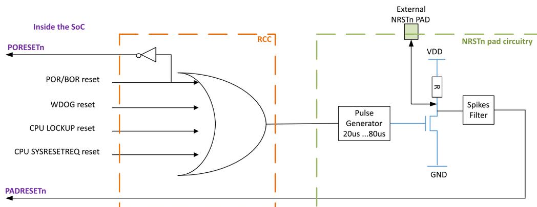
Note: The system reset information is output on the NRSTn pad to inform the external world and reset other elements on the board if needed.
Two different resets are available in the design:
- • PORESETn: this reset is provided by the LPMU analog block and corresponds to a POR or BOR root cause. It is linked to power voltage ramp-up or ramp-down. The PORESETn reset impacts all the resources of the device.
Note: A Shutdown exit is equivalent to a POR/BOR situation and generates a PORESETn.
- • PADRESETn (aka system reset): this reset is built through several sources:
- – PORESETn
- – the watchdog reset
- – the CPU LOCKUP reset
- – the CPU software system reset
- – the NRSTn external pad
Note: The system reset is called PADRESETn as when an internal reset source is activated (watchdog, software, etc.), the NRSTn pad toggles to inform the external world a reset occurs.
This system reset resets all the resources of the device except:
- • Debug features (SWD, test registers...)
- • Flash controller key management part
- • RTC timer
- • Power controller (PWR)
- • Part of the RCC registers
The pulse generator guarantees a minimum reset pulse duration of 20 µs for each internal reset source. In case of reset from the NRSTn external pad, the reset pulse is generated when the pad is asserted low.
6.1.2 Power reset
The PORESETn signal is active when the power supply of the device is below a threshold value or when the regulator does not provide the target voltage. The PORESETn resets all the resources of the device.
6.1.3 Watchdog reset
The STM32WB05xZ device embeds a watchdog timer which may be used to recover from software crashes. See Section 20: Independent watchdog (IWDG) for details about watchdog usage and programming.
6.1.4 LOCKUP reset
The Cortex-M0+ generates a LOCKUP to indicate the core is in the lock-up state resulting from an unrecoverable exception. The LOCKUP reset is masked if a debugger is connected to the Cortex-M0+. The user can use the SWD to reset or recover the code in this case.
6.1.5 System reset request
The system reset request is generated by the debug circuitry of the Cortex-M0+. The debugger sets the SYSRESETREQ bit of the application interrupt and reset control register (AIRCR). This system reset request through the AIRCR can also be done by the embedded software (in hard fault handler for instance). For more details on the Cortex-M0+ system control and ID registers, refer to section B3.2.2 of the "ARMv6-M Architecture" reference manual.
6.1.6 Deepstop exit
The low-power Deepstop state leads to switching off a part of the 1.2 V (power domain called V12i), while keeping the rest of the 1.2 V at 1 V (power domain called V12o) and the 3.3 V (VDDIO).
When the device exits the Deepstop mode, only the V12i power domain is reset as it is the only power domain that lost the power supply.
6.2 Clock management
Three different clock sources may be used to drive the system clock (CLK_SYS) in the STM32WB05xZ:
- • HSI: high speed internal 64 MHz RC oscillator (provided by the RC64MPLL analog block)
- • PLL64M: 64 MHz PLL clock (provided by the RC64MPLL analog block)
- • HSE (high speed external):
- – high speed 32 MHz external crystal
- – or provided by a single-ended 32 MHz input instead of a crystal.
The STM32WB05xZ has also a slow frequency clock tree used by some timers (RTC, watchdog, LPUART and MR_BLE radio timer). Four different clock sources can be used for this slow clock tree:
- • LSI: low speed low drift internal RC with a fixed frequency between 24 kHz and 49 kHz depending on the sample. It is called 32 kHz clock inside this document to simplify.
- • LSE:
- – 32.768 kHz low speed external crystal.
- – or provided by a single-ended 32.768 kHz input instead of a crystal.
- • The always 16 MHz clock divided by 512 (not available for LPUART). In this case, the slow clock is not available in Deepstop low-power mode
Figure 13. Clock tree generation provides an overview of the clock tree in the STM32WB05xZ.
Figure 13. Clock tree generation
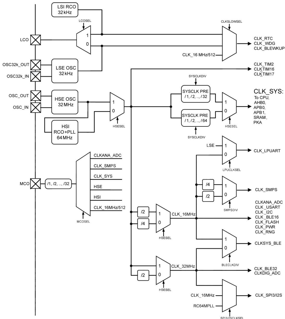
The diagram illustrates the clock tree generation within the RCC. On the left, various clock sources are shown: LSI RCO (32 kHz), LSE OSC (32 kHz), HSE OSC (32 MHz), HSI RCO+PLL (64 MHz), and MCO (output of HSE, HSI, or CLK_16MHz/512). These sources are connected to multiplexers (LOCOSEL, HSESEL, MCOSEL). The main system clock (CLK_SYS) is derived from these sources through a series of dividers (SYSCLKPRE) and multiplexers (HSESEL). The diagram also shows the generation of various peripheral clocks: CLK_RTC, CLK_WDG, CLK_BLEWKUP (from CLK_16 MHz/512); CLK_TIM2, CLK_TIM16, CLK_TIM17 (from SYSCLKDIV); CLK_SYS (to CPU, AHB0, APB0, APB1, SRAM, PKA); CLK_LPUART (from LSE); CLK_SMPS (from SMPSDIV); CLKANA_ADC, CLK_USART, CLK_I2C, CLK_BLE16, CLK_FLASH, CLK_PWR, CLK_RNG (from CLK_16MHz); CLKSYS_BLE (from CLK_16MHz); CLK_BLE32, CLKDIG_ADC (from CLK_32MHz); and CLK_SPI3/I2S (from CLK_16MHz, RC64MPLL, and SPI3I2SCLKSEL).
6.2.1 System clock details
The HSI and the PLL64M clocks are provided by the same analog block called RC64MPLL. The 64 MHz clock output by this block can be:
- • a non accurate clock (target is 1% typical) when no external XO provides an input clock to this block
- • an accurate clock when the external XO provides the 32 MHz and once its internal PLL is locked
Note: The usage of PLL64M or HSE as clock source is mandatory for Bluetooth radio operations (need of a high accuracy on the clock).
The software process to switch the system on the accurate clock is indicated in Section 6.7: Programmer model . This fast clock source is used to generate all the fast clocks of the device through dividers as shown in Figure 13. Clock tree generation .
After reset, the CLK_SYS is divided by four to provide a 16 MHz to the whole system (CPU, DMA, memories and peripherals).
Then the software can program another system clock frequency in the following list:
- • 1 MHz (forbidden when radio or ADC is in use)
- • 2 MHz (forbidden when radio or ADC is in use)
- • 4 MHz (forbidden when radio or ADC is in use)
- • 8 MHz (forbidden when radio is in use)
- • 16 MHz
- • 32 MHz
- • 64 MHz
Note: Forbidden configuration means that the “in use” feature cannot work if the system clock runs at this frequency. Special care must be taken when programming the CLK_SYS as some constraints need to be respected: CLK_SYS frequency must be greater or equal to CLK_SYS_BLE.
6.2.2 Peripheral clock details
This fast clock source is also used to generate several internal fast clocks in the system:
- • A TIM2, TIM16/17 kernel clock that is the maximum reachable frequency of the system (64 MHz in RC64MPLL configuration and 32 MHz in HSE configurations)
- • An always 32 MHz requested by few peripherals such as: the MR_BLE radio IP for instance
- • An always 16 MHz requested by few peripherals like serial interfaces (to maintain fixed baud rate while system clock is switching from one frequency to another) or like Flash controller and MR_BLE radio IP (to have a fixed reference clock to manage delays).
Most of the peripherals use the system clock only (CLK_SYS) except:
- • I2C, USART:
- – In parallel with the system clock, they use an always 16 MHz clock to have a fixed reference clock for baud rate management. The goal is to allow the CPU to boost or slow down the system clock (depending on on-going activities) without impacting a potential on-going serial interface transfer on external I/Os.
- • LPUART:
- – In parallel with the system clock, it uses an always 16 MHz clock to have a fixed reference clock for baud rate management and LSE clock when active in Deepstop. The goal is to allow the CPU to boost or slow down the system clock (depending on on-going activities) without impacting a potential on-going serial interface transfer on external I/Os.
- • SPI:
- – When using the I 2 S mode, the baud rate is managed through the always 16 MHz, always 32 MHz clock or 64 MHz clock (available only when HSESEL=0).
Note: The CPU/system clock frequency must be equal or slower than the I 2 S clock frequency.
- • When running in modes other than the I 2 S, the baud rate is managed by the system clock. This implies the baud rate is impacted by dynamic system clock frequency changes.
- • RNG:
- – In parallel with the system clock, the RNG uses an always 16 MHz clock to generate at a constant frequency the random number whatever the system clock frequency.
- • Flash controller:
- – In parallel with the system clock, the Flash controller uses an always 16 MHz clock to generate specific delays required by the Flash memory during programming and erase operation for instance.
- • MR_BLE IP:
- – MR_BLE IP does not use directly the system clock for its APB / AHB interfaces but the system clock with a potential divider (1 or 2 or 4). Table 15. CPU versus MR_BLE clock dependency shows the supported configurations.
- – In parallel with the CLK_SYS_BLE, the MR_BLE uses an always 16 MHz and an always 32 MHz for modulator, demodulator and to have a fixed reference clock to manage specific delays.
Table 15. CPU versus MR_BLE clock dependency
| CLK_SYS | CLK_SYS_BLE |
|---|---|
| 1 MHz / 2 MHz / 4 MHz / 8 MHz | Not possible to use MR_BLE IP |
| 16 MHz | 16 MHz (CLKBLEDIV = 4) |
| 32 MHz |
|
| 64 MHz |
|
- ADC
- In parallel with the system clock, the ADC uses a 64 MHz prescaled clock (called CLKANA_ADC) running at 16 MHz.
Note: When the ADC is used, the system clock must run at minimum 8 Mhz to be able to read the ADC sample before they are overloaded by a new sample.
Note: To avoid SNR degradation of the ADC, SMPS and ADC clocks must be synchronous.
6.2.3 Slow clock frequency details
As explained at the beginning of the clock management sub-section, four different clock sources can be used for this slow clock tree:
- LSI: low speed low drift internal RC with a fixed frequency between 24 kHz and 49 kHz depending on the sample. It is called 32 kHz clock inside this document to simplify.
- LSE: 32.768 kHz low speed external crystal (or single-ended input frequency).
Note: If the external oscillator is used, the PB12/PB13 I/Os are automatically connected to this feature when RCC_CR.LSEON bit is set (GPIO_MODERX configuration is overloaded).
Caution: If APC bit is set, the user has to disable the PUB12/PUB13/PDB12/PDB13 bits on PB12/PB13 by software I/O Port B pull-up control register (PWRC_PUCRB) to have the feature working well. Otherwise, if APC is reset, the pull-up, pull-down of PB12/13 are automatically configured.
- An always 32 kHz clock equal to HSI/2048 if HSESEL='0' or else HSE/1024. In this case, the slow clock is not available in Deepstop low-power mode
Only one source at a time drives the whole low speed clock tree.
Note: By default after a PORESETn, all low speed sources are OFF. After a PADRESETn, the slow clock configuration is the one programmed before the PADRESETn.
The slow clock activation and selection are relevant during the Deepstop low-power mode and at wakeup as they clock the timers involved in wakeup events generation.
Note: If LSI configuration is used, the software must measure the slow clock frequency to know the associated period that is used by the timers. A slow clock measurement feature is available in the MR_BLE IP.
6.3 System frequency switch while MR_BLE is used
The CPU/system clock frequency can be from 1 MHz to 64 MHz while the MR_BLE clock frequency can be 16 MHz or 32 MHz.
When the radio is used on the device, the system clock frequency selection must respect some rules:
- the system clock frequency must be 16 MHz, 32 MHz or 64 MHz and greater than or equal to the MR_BLE frequency. Other options make the radio not functional.
- changing the frequency of the system must be done through the RCC_CSCMDR register mechanism to avoid any risk of crashing the radio scenarios.
This proper system frequency switch is managed through the collaboration of several blocks:
- the RCC (see Section 6.6.6: Clock switch command register (RCC_CSCMDR) )
- the AHBUPCONV and the AHBDOWNCONV blocks (see Section 3: AHB up/down converter )
Using this safe mechanism, the software requests a system clock frequency change and is informed by the hardware when the new frequency is really in place through a status bit (see Section 6.6.6: Clock switch command register (RCC_CSCMDR) ) and an associated interrupt line on the CPU (see Section 2.3.2: Interrupts ).
The software sequence is described in Section 6.7.3: Changing the system clock frequency while the MR_BLE is enabled .
6.4 Clock observation on external pad
It is possible to output some internal clocks on external pads:
- • the low speed clocks can be output on the RCC_LCO I/O
- • the high speed clocks can be output on the RCC_MCO I/O
This is possible by programming the associated I/O in the good alternate function (see Table 7. GPIO alternate options AF0, AF1 and AF2 modes and Table 8. GPIOs AF3, AF4 and AF6 modes ).
The selection of the clock to output for each I/O is programmable through an RCC register (see Section 6.6: RCC registers for more details).
Figure 14. RCC_LCO / RCC_MCO output clocks shows the possible configurations to output an internal clock.
Figure 14. RCC_LCO / RCC_MCO output clocks
![Block diagram showing the configuration for RCC_LCO and RCC_MCO output clocks. The top part shows LSI and LSE inputs to a multiplexer controlled by RCC_CFGR.LCOSE[1:0], outputting to RCC_LCO. The bottom part shows multiple clock inputs (CLKANA_ADC, CLK_SMPS, CLK_SYS, HSE, HSI, CLK_16MHz/512) to a multiplexer controlled by RCC_CFGR.MCOSEL[2:0]. The output of this multiplexer goes to a prescaler block (/1, /2, /4, /8, /16, /32) controlled by RCC_CFGR.CCOPRE[2:0], which then outputs to RCC_MCO.](/RM0529-STM32WB05xZ/faa6766e9ed23a192edcbbbbb753e88c_img.jpg)
DT56431V1
6.5 Miscellaneous
6.5.1 IO BOOSTER
Some analog switches are used to select the analog VINM/P pair input signals to be used by the ADC.
An IO BOOSTER block has been added to boost the voltage on the command of those analog switches when the VBAT goes below a threshold (2.7 V) to guarantee the good behavior of those switches. This block has to be enabled by the software when needed through RCC_CFGR.IOBOOSTEN bit.
6.6 RCC registers
Refer to Table 3. STM32WB05xZ memory map and peripheral register boundary addresses for the RCC base address location in the STM32WB05xZ.
6.6.1 Clock source control register (RCC_CR)
This register controls the enable on the different clock sources (low and high speed).
Note: The control bits linked to high speed clock source are reset on PADRESETn. The control bits linked to slow speed clock source are reset on PORESETn only (identified by the table footnote). As this register is in V12o power domain, its content is not modified after a wakeup from Deepstop and system clock is restored with configuration present before Deepstop mode entry.
Address offset: 0x00
Reset value: 0x0000 1400
| 31 | 30 | 29 | 28 | 27 | 26 | 25 | 24 | 23 | 22 | 21 | 20 | 19 | 18 | 17 | 16 |
|---|---|---|---|---|---|---|---|---|---|---|---|---|---|---|---|
| Res. | Res. | Res. | Res. | Res. | Res. | Res. | Res. | Res. | Res. | Res. | Res. | Res. | Res. | HSERDY | HSEON |
| r | rw | ||||||||||||||
| 15 | 14 | 13 | 12 | 11 | 10 | 9 | 8 | 7 | 6 | 5 | 4 | 3 | 2 | 1 | 0 |
| Res. | HSIPLL RDY | HSIPLL ON | HSEPLL BUFON | Res. | HSIRDY | LOCKDET_NSTOP | LSEBYP | LSERDY | LSEON | LSIRDY | LSION | Res. | Res. | ||
| r | rw | rw | r | rw | rw | r | rw | r | rw | ||||||
| Bits 31:18 | Reserved, must be kept at reset value. |
| Bit 17 | HSERDY:
External high speed clock flag. This bit is set by hardware to indicate that HSE oscillator (32 MHz XO) is stable.
|
| Bit 16 | HSEON:
External high speed clock enable. The software has to set the bit to start the XO 32 MHz and clear the bit to stop it.
|
| Bit 15 | Reserved, must be kept at reset value. |
| Bit 14 | HSIPLL RDY:
Internal high speed clock PLL flag. This bit is set by hardware to indicate that the RC64MPLL pll is locked.
|
| Bit 13 | HSIPLL ON:
Internal high speed clock PLL enable. The software has to set the bit to request an RC64MPLL lock on HSE and clear the bit to stop it.
|
| Bit 12 | HSEPLL BUFON:
External high speed clock buffer for PLL RF2G4 enable. The software has to set the bit when the radio is used (to have the 2.4 GHz PLL working).
|
| Warning: This bit must be set when the radio is used. The only reason to clear this bit would be to reduce power consumption for application not using the radio on this device. | |
| Bit 11 | Reserved, must be kept at reset value. |
| Bit 10 | HSIRDY:
Internal high speed clock flag. This bit is set by hardware to indicate that internal 64 MHz RC is stable.
|
| Bits 9:7 | LOCKDET_NSTOP:
Defines a time window target for the counter of the lock detector block in charge to manage the HSIPLLRDY information (PLL indicated as locked if the analog lock signal stays high and stable during this time window). The formula to define the time window target is the following: \[
\text{time window target} = (\text{LOCKDET\_NSTOP} + 1) \times 64.
\] |
| Bit 6 (1)(2) | LSEBYP:
External low speed clock bypass. This bit needs to be set when the slow clock is directly provided through RCC_OSC32_IN pin.
|
| Bit 5 (1) | LSERDY:
External low speed clock flag. This bit is set by hardware to indicate that the slow clock has started.
|
| Bit 4 (1)(2) | LSEON:
External low speed clock enable. The software has to set the bit to start the XO 32 kHz and clear the bit to stop it.
|
| Bit 3 (1) | LSIRDY:
Internal low speed clock flag. This bit is set by hardware to indicate that internal low speed RC is stable.
|
| Bit 2 (1) | LSION:
Internal low speed RC clock enable. The software has to set the bit to start the internal slow clock RO and clear the bit to stop it.
|
| Bits 1:0 | Reserved, must be kept at reset value. |
1. This bit is reset on PORESETn and when the low speed clock is disabled at runtime.
2. The LSEBYP and LSEON bits must not be used at the same time. If the user decides to dynamically change the slow clock source between external XO and clock injection on RCC_OSC32_IN, they have to ensure both LSEON and LSEBYP are low at a time to reset the LSERDY flag.
6.6.2 Clocks configuration register (RCC_CFGR)
Note: The control bits linked to high speed clock source are reset on PADRESETn. The control bits linked to slow speed clock source are reset on PORESETn only (identified by the table footnote).
Address offset: 0x08
Reset value: 0x0000 0240
| 31 | 30 | 29 | 28 | 27 | 26 | 25 | 24 | 23 | 22 | 21 | 20 | 19 | 18 | 17 | 16 |
|---|---|---|---|---|---|---|---|---|---|---|---|---|---|---|---|
| CCOPRE[2:0] | MCOSEL[2:0] | LCOSEL[1:0] | SPI3I2SCLKSEL [1:0] | Res. | Res. | LCOEN | OBOOSTCLKEN | IOBOOSTEN | CLKSLOWSEL[1] | ||||||
| rw | rw | rw | rw | rw | rw | rw | rw | rw | rw | rw | rw | rw | rw | ||
| 15 | 14 | 13 | 12 | 11 | 10 | 9 | 8 | 7 | 6 | 5 | 4 | 3 | 2 | 1 | 0 |
| CLKSLOWSEL[0] | Res. | LPUCLKSEL | SMPSDIV | Res. | CLKSYSDIV_STATUS[2:0] | CLKSYSDIV[2:0] | Res. | HSESEL_STATUS | STOPHSI | HSESEL | Res. | ||||
| rw | rw | rw | r | r | r | rw | rw | rw | r | rw | rw | ||||
| Bits 31:29 | CCOPRE: Configurable clock output prescaler.
Note: Glitches propagation possible if CCOPRE[2:0] value is modified while RCC_MCO output is enabled on the IO. |
| Bits 28:26 | MCOSEL: Main configurable clock output selection.
Note: Glitches propagation possible if MCOSEL[2:0] value is modified while RCC_MCO output is enabled on the IO. |
| Bits 25:24 (1) | LCOSEL: Low speed configurable clock output selection.
|
| Note: Glitches propagation possible if LCOSEL[1:0] value is modified while RCC_LCO output is enabled on the IO. | |
| Bit 23:22 | SPI3I2SCLKSEL[1:0]
: Selection of I
2
S clock for SPI3 IP.
|
| Bits 21:20 | Reserved, must be kept at reset value. |
| Bit 19 (1) | LCOEN
: RCC_LCO enable on PA10 also in deepstop.
|
| Bit 18 | IOBOOSTCKEN
: IO BOOSTER clock enable (see
Section 6.5.1: IO BOOSTER
for details).
|
| Bit 17 | IOBOOSTEN
: IO BOOSTER enable (see
Section 6.5.1: IO BOOSTER
for details).
|
| Bits 16:15 (1) | CLKSLOWSEL
: Low speed clock source selection.
|
| Bit 14 | Reserved, must be kept at reset value. |
| Bit 13 (1) | LPUCLKSEL
: Selection of LPUART clock
|
| Bit 12 | SMPSDIV
: SMPS clock prescaling factor.
|
| Bit 11 | Reserved, must be kept at reset value. |
| Bit 10:8 | CLKSYSDIV_STATUS
: system clock frequency status. Set and cleared by hardware to indicate the actual system clock frequency. This register must be read to be sure that the new frequency, selected by CLKSYSDIV, has been applied.
|
| Bits 7:5 | CLKSYSDIV
: System clock divided factor from HSI_64M.
|
*: If RCC_APB2ENR.MRBLEEN bit is set, writing in CLKSYSDIV one of those values is replaced by a 010b = 16 MHz writing at hardware level. Warning:
| |
| Bit 4 | Reserved, must be kept at reset value. |
| Bit 3 | HSESEL_STATUS
: Clock source selection status.
|
| Bit 2 | STOPHSI
: RC64MPLL clock source stop request
Note: If the CLKSYSDIV (from RCC_CFGR or RCC_CSCMDR registers) selects the 64 MHz frequency, the hardware automatically restarts the RC64MPLL block and switches on the RC64MPLL clock source. |
| Bit 1 | HSESEL
: Clock source selection request.
In this case, the fast clock tree is sourced by the RC64MPLL block. The clock can be either the HSI or the PLL64M if the HSI PLL is locked.
In this case, the RC64MPLL block is not used and the maximum available frequency for the system clock tree is 32 MHz. |
| Bit 0 | Reserved, must be kept at reset value. |
1. This bit is reset on PORESETn only.
6.6.3 Clocks Sources Software Calibration register (RCC_CSSWCR)
This register allows overloading the trimming values loaded automatically by hardware with other values.
Note: The control bits linked to high speed clock source are reset on PADRESETn. The control bits linked to high speed clock source are reset on PORESETn only (identified by the table footnote).
Address offset: 0x0C
Reset value: 0x0000 0000
| 31 | 30 | 29 | 28 | 27 | 26 | 25 | 24 | 23 | 22 | 21 | 20 | 19 | 18 | 17 | 16 |
|---|---|---|---|---|---|---|---|---|---|---|---|---|---|---|---|
| Res. | Res. | HSITRIMSW[5:0] | HSISWTRIMEN | Res. | Res. | Res. | Res. | Res. | Res. | Res. | |||||
| rw | rw | rw | rw | rw | rw | rw | |||||||||
| 15 | 14 | 13 | 12 | 11 | 10 | 9 | 8 | 7 | 6 | 5 | 4 | 3 | 2 | 1 | 0 |
| Res. | Res. | Res. | Res. | Res. | Res. | Res. | Res. | Res. | LSEDRV | LSISWBW[3:0] | LSISWTRIMEN | ||||
| rw | rw | rw | rw | rw | rw | rw | |||||||||
| Bits 31:30 | Reserved, must be kept at reset value. |
| Bits 29:24 | HSITRIMSW:
High speed clock trimming set by software. This value is taken into account instead of the trimming value loaded by HW at reset if HSISWTRIMEN bit is set. |
| Bit 23 | HSISWTRIMEN:
High speed clock software trimming enable. 0: HW trimming value readable in RCC_ICSCR.HSITRIM[3:0] bit field is used as trimming value on RC64MPLL block. 1: trimming value written in RCC_CSSWCR.HSITRIMSW[3:0] bit field is used as trimming value on RC64MPLL block. |
| Bits 22:7 | Reserved, must be kept at reset value. |
| Bits 6:5 (1) | LSEDRV:
external 32 kHz crystal GM.
|
| Bits 4:1 (1) | LSISWBW:
Low speed internal RC trimming value set by software. This value is taken into account instead of the trimming value loaded by HW at reset if LSISWTRIMEN bit is set. |
| Bit 0 (1) | LSISWTRIMEN:
Low speed internal RC software trimming enable.
|
1. This bit is reset on PORESETn only.
6.6.4 Clock interrupt enable register (RCC_CIER)
This register controls the enable on interrupt sources.
This register is reset on PADRESETn.
Address offset: 0x18
Reset value: 0x0000 0000
| 31 | 30 | 29 | 28 | 27 | 26 | 25 | 24 | 23 | 22 | 21 | 20 | 19 | 18 | 17 | 16 |
|---|---|---|---|---|---|---|---|---|---|---|---|---|---|---|---|
| Res. | Res. | Res. | Res. | Res. | Res. | Res. | Res. | Res. | Res. | Res. | Res. | Res. | Res. | Res. | Res. |
| 15 | 14 | 13 | 12 | 11 | 10 | 9 | 8 | 7 | 6 | 5 | 4 | 3 | 2 | 1 | 0 |
| Res. | Res. | Res. | Res. | Res. | Res. | LPURSTIE | WDGRSTIE | RTCIRSTIE | HSIPLLUNLOCKDETIE | HSIPLLRDYIE | HSERDYIE | HSIRDYIE | Res. | LSERDYIE | LSIRDYIE |
| r/w | r/w | r/w | r/w | r/w | r/w | r/w | r/w | r/w |
| Bits 31:10 | Reserved, must be kept at reset value. |
| Bit 9 | LPURSTIE:
LPUART reset release interrupt enable.
|
| Bit 8 | WDGRSTIE:
Watchdog reset release interrupt enable.
|
| Bit 7 | RTCIRSTIE:
RTC reset release interrupt enable.
|
| Bit 6 | HSIPLLUNLOCKDETIE:
HSI PLL unlock detection interrupt enable.
|
| Bit 5 | HSIPLLRDYIE:
HSI PLL ready interrupt enable.
|
| Bit 4 | HSERDYIE:
HSE ready interrupt enable.
|
| Bit 3 | HSIRDYIE:
HSI ready interrupt enable.
|
| Bit 2 | Reserved, must be kept at reset value. |
| Bit 1 | LSERDYIE:
LSE ready interrupt enable.
|
| Bit 0 | LSIRDYIE:
LSI ready interrupt enable.
|
6.6.5 Clock interrupt flag register (RCC_CIFR)
This register provides the status flag linked to clock source ready state or not. It is also used to clear the flags.
This register is reset on PADRESETn.
Address offset: 0x1C
Reset value: 0x0000 0008
| 31 | 30 | 29 | 28 | 27 | 26 | 25 | 24 | 23 | 22 | 21 | 20 | 19 | 18 | 17 | 16 |
|---|---|---|---|---|---|---|---|---|---|---|---|---|---|---|---|
| Res. | Res. | Res. | Res. | Res. | Res. | Res. | Res. | Res. | Res. | Res. | Res. | Res. | Res. | Res. | Res. |
| 15 | 14 | 13 | 12 | 11 | 10 | 9 | 8 | 7 | 6 | 5 | 4 | 3 | 2 | 1 | 0 |
| Res. | Res. | Res. | Res. | Res. | Res. | LPURSTF | WDGRSTF | RTCSTF | HSIPLLUNLOCKDETF | HSIPLLRDYF | HSERDYF | HSIRDYF | Res. | LSERDYF | LSIRDYF |
| rc_w1 | rc_w1 | rc_w1 | rc_w1 | rc_w1 | rc_w1 | rc_w1 | rc_w1 | rc_w1 |
| Bits 31:10 | Reserved, must be kept at reset value. |
| Bit 9 | LPURSTF: LPUART reset release flag.
Note: due to asynchronism slow clock/fast clock management, when the software request to release the LPUART reset by writing in the RCC_APB0RSTR.LPUARTRST, the reset release is effective only 2 slow clock periods or 2 16 MHz clock periods after the APB writing, depending on how it's configured LPCLKSEL bit in Clocks Configuration register (RCC_CFGR). This interrupt allows the software to be informed when the reset release is really done. Note: this flag is also set after any PORESETn. |
| Bit 8 | WDGRSTF: Watchdog reset release flag.
Note: Due to asynchronism slow clock/fast clock management, when the software request to release the Watchdog reset by writing in the RCC_APB0RSTR.WDGRST, the reset release is effective only 2 slow clock periods after the APB writing. This interrupt allows informing the software when the reset release is really done. Note: This flag is also set after any PORESETn. |
| Bit 7 | RTCSTF: RTC reset release flag.
Note: Due to asynchronism slow clock/fast clock management, when the software request to release the RTC reset by writing in the RCC_APB0RSTR.RTCRST, the reset release is effective only 2 slow clock periods after the APB writing. This interrupt allows informing the software when the reset release is really done. Note: This flag is also set after any PORESETn. |
| Bit 6 | HSIPLLUNLOCKDETF: HSI PLL unlock detection flag.
|
| Bit 5 | HSIPLLRDYF: HSI PLL ready flag.
|
| Bit 4 | HSERDYF: HSE ready flag.
|
| Bit 3 | HSIRDYF:
HSI ready flag.
|
| Bit 2 | Reserved, must be kept at reset value. |
| Bit 1 | LSERDYF:
LSE ready flag.
|
| Bit 0 | LSIRDYF:
LSI ready flag.
|
6.6.6 Clock switch command register (RCC_CSCMDR)
This register allows switching the CPU / system clock frequency safely while the MR_BLE is active.
Requesting a frequency clock switch holds the AHB/APB transfers between the MR_BLE and the rest of the system to execute safely the clock switching and release AHB / APB transfers as soon as the new frequency is in place.
A dedicated line of interrupt (instead of the RCC line) is used on the NVIC for the EOFSEQ_IRQ information (see Table 6. Interrupt vectors).
Note: Anyway, the user must keep the CPU/system frequency at minimum 16 MHz clock when the radio is used.
This register is reset on PADRESETn.
Address offset: 0x20
Reset value: 0x0000 0080
| 31 | 30 | 29 | 28 | 27 | 26 | 25 | 24 | 23 | 22 | 21 | 20 | 19 | 18 | 17 | 16 |
|---|---|---|---|---|---|---|---|---|---|---|---|---|---|---|---|
| Res. | Res. | Res. | Res. | Res. | Res. | Res. | Res. | Res. | Res. | Res. | Res. | Res. | Res. | Res. | Res. |
| 15 | 14 | 13 | 12 | 11 | 10 | 9 | 8 | 7 | 6 | 5 4 | 3 2 1 | 0 | |||
| Res. | Res. | Res. | Res. | Res. | Res. | Res. | Res. | EOFSEQ_IRQ | EOFSEQ_IE | STATUS[1:0] | CLKSYSDIV_REQ[2:0] | REQUEST | |||
| rc_w1 | rw | r | r | rw | rw | rw | rw | ||||||||
| Bits 31:8 | Reserved, must be kept at reset value. |
| Bit 7 | EOFSEQ_IRQ:
End of sequence flag.
|
| Bit 6 | EOFSEQ_IE:
End of sequence interrupt enable.
|
| Bits 5:4 | STATUS:
Status of the switching sequence.
This bit field is cleared when EOFSEQ_IRQ bit is cleared. |
| Bits 3:1 | CLKSYSDIV_REQ:
System clock requested/targeted frequency. Same format and same notes/warnings as SYSCLKDIV[2:0] bit field described in Section 6.6.2: Clocks configuration register (RCC_CFGR) . |
| Bit 0 | REQUEST:
request to switch the system clock frequency. Write 1 in this bit to request a system clock frequency switch (using CLKSYSDIV_REQ[2:0] information). This bit is cleared by hardware when the clock frequency switch is done. Note: Writing 0 in this bit aborts the frequency switch sequence if it is not yet finished. This action must not be used in the normal life of the application except if the end of sequence does not occur after a long time (to unblock the situation) but this is not supposed to occur. |
6.6.7 AHB0 macro cells reset register (RCC_AHBRSTR)
This register allows resetting individually by software each IP located in the AHB0 mapping. This register is reset on PADRESETn.
Address offset: 0x30
Reset value: 0x0000 0000
| 31 | 30 | 29 | 28 | 27 | 26 | 25 | 24 | 23 | 22 | 21 | 20 | 19 | 18 | 17 | 16 |
|---|---|---|---|---|---|---|---|---|---|---|---|---|---|---|---|
| Res. | Res. | Res. | Res. | Res. | Res. | Res. | Res. | Res. | Res. | Res. | Res. | Res. | RNGRST | Res. | PKARST |
| rw | rw | ||||||||||||||
| 15 | 14 | 13 | 12 | 11 | 10 | 9 | 8 | 7 | 6 | 5 | 4 | 3 | 2 | 1 | 0 |
| Res. | Res. | Res. | CRCRST | Res. | Res. | Res. | Res. | Res. | Res. | Res. | Res. | GPIOBRST | GPIOARST | Res. | DMARST |
| rw | rw | rw | rw |
| Bits 31:19 | Reserved, must be kept at reset value. |
| Bit 18 | RNGRST:
RNG reset.
|
| Bit 17 | Reserved, must be kept at reset value. |
| Bit 16 | PKARST:
PKA reset.
|
| Bits 15:13 | Reserved, must be kept at reset value |
| Bit 12 | CRCRST:
CRC reset.
|
| Bits 11:4 | Reserved, must be kept at reset value. |
| Bit 3 | GPIOBRST:
IO controller for port B reset.
|
| Bit 2 | GPIOARST:
IO controller for port A reset.
|
| Bit 1 | Reserved, must be kept at reset value. |
| Bit 0 | DMARST:
DMA and DMAMUX reset.
|
6.6.8 APB0 macro cells reset register (RCC_APB0RSTR)
This register allows resetting individually by software each IP located in the APB0 mapping. This register is reset on PADRESETn.
Note: Each bit is set and reset by the software.
Address offset: 0x34
Reset value: 0x0000 0000
| 31 | 30 | 29 | 28 | 27 | 26 | 25 | 24 | 23 | 22 | 21 | 20 | 19 | 18 | 17 | 16 |
|---|---|---|---|---|---|---|---|---|---|---|---|---|---|---|---|
| Res. | Res. | Res. | Res. | Res. | Res. | Res. | Res. | Res. | Res. | Res. | Res. | Res. | Res. | Res. | Res. |
| 15 | 14 | 13 | 12 | 11 | 10 | 9 | 8 | 7 | 6 | 5 | 4 | 3 | 2 | 1 | 0 |
|---|---|---|---|---|---|---|---|---|---|---|---|---|---|---|---|
| Res. | WDGRST | Res. | RTCRST | Res. | Res. | Res. | SYSCFGRST | Res. | Res. | Res. | Res. | Res. | TIM17RST | TIM16RST | TIM2RST |
| rw | rw | rw | rw | rw | rw |
| Bits 31:15 | Reserved, must be kept at reset value. |
| Bit 14 | WDGRST
: Watchdog reset.
|
| Bit 13 | Reserved, must be kept at reset value. |
| Bit 12 | RTCRST
: RTC reset.
|
| Bits 11:9 | Reserved, must be kept at reset value. |
| Bit 8 | SYSCFGRST
: System controller reset.
|
| Bits 7:3 | Reserved, must be kept at reset value. |
| Bit 2 | TIM17RST
: TIM17 reset.
|
| Bit 1 | TIM16RST
: TIM16 reset.
|
| Bit 0 | TIM2RST
: TIM2 reset.
|
6.6.9 APB1 macro cells reset register (RCC_APB1RSTR)
This register allows resetting individually by software each IP located in the APB1 mapping. This register is reset on PADRESETn.
Address offset: 0x38
Reset value: 0x0000 0000
| 31 | 30 | 29 | 28 | 27 | 26 | 25 | 24 | 23 | 22 | 21 | 20 | 19 | 18 | 17 | 16 |
|---|---|---|---|---|---|---|---|---|---|---|---|---|---|---|---|
| Res. | Res. | Res. | Res. | Res. | Res. | Res. | Res. | Res. | Res. | I2C1RST | Res. | Res. | Res. | Res. | Res. |
| rw | |||||||||||||||
| 15 | 14 | 13 | 12 | 11 | 10 | 9 | 8 | 7 | 6 | 5 | 4 | 3 | 2 | 1 | 0 |
| Res. | SPI3RST | Res. | Res. | Res. | USARTRST | Res. | LPUARTRST | Res. | Res. | Res. | ADCRST | Res. | Res. | Res. | Res. |
| rw | rw | rw | rw |
| Bits 31:22 | Reserved, must be kept at reset value. |
| Bit 21 | I2C1RST
: I2C1 reset.
|
| Bits 20:15 | Reserved, must be kept at reset value. |
| Bit 14 | SPI3RST
: SPI3 reset.
|
| Bits 13:11 | Reserved, must be kept at reset value. |
| Bit 10 | USARTRST
: USART reset.
|
| Bit 9 | Reserved, must be kept at reset value. |
| Bit 8 | LPUARTRST
: LPUART reset.
|
| Bits 7:5 | Reserved, must be kept at reset value. |
| Bit 4 | ADCRST
: ADC reset.
|
| Bits 3:0 | Reserved, must be kept at reset value. |
6.6.10 APB2 macro cells reset register (RCC_APB2RSTR)
This register allows resetting individually by software each IP located in the APB2 mapping (radio).
This register is reset on PADRESETn.
Address offset: 0x40
Reset value: 0x0000 0000
| 31 | 30 | 29 | 28 | 27 | 26 | 25 | 24 | 23 | 22 | 21 | 20 | 19 | 18 | 17 | 16 |
| Res. | Res. | Res. | Res. | Res. | Res. | Res. | Res. | Res. | Res. | Res. | Res. | Res. | Res. | Res. | Res. |
| 15 | 14 | 13 | 12 | 11 | 10 | 9 | 8 | 7 | 6 | 5 | 4 | 3 | 2 | 1 | 0 |
| Res. | Res. | Res. | Res. | Res. | Res. | Res. | Res. | Res. | Res. | Res. | Res. | Res. | Res. | Res. | MRBLERST |
| Bits 31:1 | Reserved, must be kept at reset value. |
| Bit 0 | MRBLERST:
MR_BLE (Bluetooth radio) reset.
|
6.6.11 AHB0 macro cells clock enable register (RCC_AHBENR)
This register allows resetting individually by software each IP located in the AHB0 mapping.
Note: Each IP clock gating is controlled by only 1 bit which gates both AHB clock and kernel clock when the IP uses one.
This register is reset on PADRESETn.
Address offset: 0x50
Reset value: 0x0000 000C
| 31 | 30 | 29 | 28 | 27 | 26 | 25 | 24 | 23 | 22 | 21 | 20 | 19 | 18 | 17 | 16 |
| Res. | Res. | Res. | Res. | Res. | Res. | Res. | Res. | Res. | Res. | Res. | Res. | Res. | RNGREN | Res. | PKAEN |
| rw | rw | ||||||||||||||
| 15 | 14 | 13 | 12 | 11 | 10 | 9 | 8 | 7 | 6 | 5 | 4 | 3 | 2 | 1 | 0 |
| Res. | Res. | Res. | CREN | Res. | Res. | Res. | Res. | Res. | Res. | Res. | Res. | GPIOBEN | GPIOAEN | Res. | DMAEN |
| rw | rw | rw | rw |
| Bits 31:19 | Reserved, must be kept at reset value. |
| Bit 18 | RNGEN:
RNG clock enable.
|
| Bit 17 | Reserved, must be kept at reset value. |
| Bit 16 | PKAEN:
PKA enable.
|
| Bits 15:13 | Reserved, must be kept at reset value. |
| Bit 12 | CREN:
CRC enable.
|
| Bits 11:4 | Reserved, must be kept at reset value. |
| Bit 3 | GPIOBEN:
IO controller for port B enable.
|
| Bit 2 | GPIOAEN:
IO controller for port A enable.
|
| Bit 1 | Reserved, must be kept at reset value. |
| Bit 0 | DMAEN:
DMA and DMAMUX enable.
|
6.6.12 APB0 macro cell clock enable register (RCC_APB0ENR)
This register allows gating individually by software the clock of each IP located in the APB0 mapping.
Note: Each IP clock gating is controlled by only 1 bit, which gates both APB clock and kernel clock when the IP uses one.
This register is reset on PADRESETn (except one bit identified with a table footnote).
Address offset: 0x54
Reset value: 0x0000 0000
| 31 | 30 | 29 | 28 | 27 | 26 | 25 | 24 | 23 | 22 | 21 | 20 | 19 | 18 | 17 | 16 |
|---|---|---|---|---|---|---|---|---|---|---|---|---|---|---|---|
| Res. | Res. | Res. | Res. | Res. | Res. | Res. | Res. | Res. | Res. | Res. | Res. | Res. | Res. | Res. | Res. |
| 15 | 14 | 13 | 12 | 11 | 10 | 9 | 8 | 7 | 6 | 5 | 4 | 3 | 2 | 1 | 0 |
| Res. | WDGEN | Res. | RTCEN | Res. | Res. | Res. | SYSCFGEN | Res. | Res. | Res. | Res. | Res. | TIM17EN | TIM16EN | TIM2EN |
| rw | rw | rw | rw | rw | rw |
| Bits 31:15 | Reserved, must be kept at reset value. |
| Bit 14 | WDGEN:
Watchdog enable.
|
| Bit 13 | Reserved, must be kept at reset value. |
| Bit 12 (1) | RTCEN:
RTC enable.
|
| Bit 11:9 | Reserved, must be kept at reset value. |
| Bits 8 | SYSCFGEN:
System controller enable.
|
| Bits 7:3 | Reserved, must be kept at reset value |
| Bit 2 | TIM17EN:
TIM17 enable
|
| Bit 1 | TIM16EN:
TIM16 enable
|
| Bit 0 | TIM2EN:
TIM2 enable
|
1. This bit is reset on PORESETn only.
6.6.13 APB1 macro cells clock enable register (RCC_APB1ENR)
This register allows gating individually by software the clock of each IP located in the APB1 mapping.
Note: Each IP clock gating is controlled by only 1 bit, which gates both APB clock and kernel clock when the IP uses one.
This register is reset on PADRESETn.
Address offset: 0x58
Reset value: 0x0000 0000
| 31 | 30 | 29 | 28 | 27 | 26 | 25 | 24 | 23 | 22 | 21 | 20 | 19 | 18 | 17 | 16 |
|---|---|---|---|---|---|---|---|---|---|---|---|---|---|---|---|
| Res. | Res. | Res. | Res. | Res. | Res. | Res. | Res. | Res. | Res. | I2C1EN | Res. | Res. | Res. | Res. | Res. |
| rw | |||||||||||||||
| 15 | 14 | 13 | 12 | 11 | 10 | 9 | 8 | 7 | 6 | 5 | 4 | 3 | 2 | 1 | 0 |
| Res. | SPI3EN | Res. | Res. | Res. | USARTEN | Res. | LPUARTEN | Res. | Res. | ADCANAEN | ADCDIGEN | Res. | Res. | Res. | Res. |
| rw | rw | rw | rw | rw |
| Bits 31:2 | Reserved, must be kept at reset value. |
| Bit 21 | I2C1EN:
I2C1 enable.
|
| Bits 20:15 | Reserved, must be kept at reset value. |
| Bit 14 | SPI3EN:
SPI3 enable.
|
| Bit 13:11 | Reserved, must be kept at reset value. |
| Bit 10 | USARTEN:
USART enable.
|
| Bit 9 | Reserved, must be kept at reset value. |
| Bit 8 | LPUARTEN:
LPUART enable.
WARNING: the software has to wait for 2 slow clock cycles before using the LPUART IP after setting this bit due to a double resynchronization on slow clock. |
| Bits 7:6 | Reserved, must be kept at reset value. |
| Bit 5 | ADCANAEN:
ADC clock enable for the analog part of the ADC block.
|
| Bit 4 | ADCDIGEN
ADC clock enable for digital part of the ADC block.
|
| Bits 3:0 | Reserved, must be kept at reset value. |
6.6.14 APB2 macro cells clock enable register (RCC_APB2ENR)
This register allows gating by software the MR_BLE clock located in the APB2 mapping (radio) and programming the frequency to be used by the MR_BLE IP.
Note: Gating the MR_BLE means both MR_BLE fast and slow clock trees (so including WAKEUP block).
This register is reset on PADRESETn.
Address offset: 0x60
Reset value: 0x0000 0000
| 31 | 30 | 29 | 28 | 27 | 26 | 25 | 24 | 23 | 22 | 21 | 20 | 19 | 18 | 17 | 16 |
| Res. | Res. | Res. | Res. | Res. | Res. | Res. | Res. | Res. | Res. | Res. | Res. | Res. | Res. | Res. | Res. |
| 15 | 14 | 13 | 12 | 11 | 10 | 9 | 8 | 7 | 6 | 5 | 4 | 3 | 2 | 1 | 0 |
| Res. | Res. | Res. | Res. | Res. | Res. | Res. | Res. | Res. | Res. | Res. | Res. | Res. | CLKBLEDIV | Res. | MRBLEEN |
| rw | rw | ||||||||||||||
| Bits 31:3 | Reserved, must be kept at reset value. |
| Bit 2 | CLKBLEDIV: MR_BLE (Bluetooth ® LE radio) clock frequency selection when RCC_APB2ENR.MRBLEEN=1.
Note: Writing “00” by software is replaced by a write “01” in hardware.
Warning:
For this reason, using a static MR_BLE clock configuration is strongly recommended. |
| Bit 1 | Reserved, must be kept at reset value |
| Bit 0 | MRBLEEN: MR_BLE (Bluetooth ® LE radio) enable.
|
6.6.15 V33 reset status register (RCC_CSR)
This register provides the reset reason flags. It is set automatically by hardware on any new reset event and must be cleared by software.
Table 13. Flags versus CPU reboot reason provides a summary of active flags versus reset reason.
This register is reset on PORESETn.
Address offset: 0x94
Reset value: 0x0C00 0000
| 31 | 30 | 29 | 28 | 27 | 26 | 25 | 24 | 23 | 22 | 21 | 20 | 19 | 18 | 17 | 16 |
|---|---|---|---|---|---|---|---|---|---|---|---|---|---|---|---|
| Res. | LOCKUPRSTF | WDGRSTF | SFTRSTF | PORRSTF | PADRSTF | Res. | Res. | RMVF | Res. | Res. | Res. | Res. | Res. | Res. | Res. |
| r | r | r | r | r | rc_w1 | ||||||||||
| 15 | 14 | 13 | 12 | 11 | 10 | 9 | 8 | 7 | 6 | 5 | 4 | 3 | 2 | 1 | 0 |
| Res. | Res. | Res. | Res. | Res. | Res. | Res. | Res. | Res. | Res. | Res. | Res. | Res. | Res. | Res. | Res. |
| Bit 31 | Reserved, must be kept at reset value. |
| Bit 30 | LOCKUPRSTF
: CPU lock-up reset flag. Set by the hardware when a CPU lock-up reset occurs. Reset by writing 1 in RMVF bit. |
| Bit 29 | WDGRSTF
: Watchdog reset flag. Set by the hardware when a watchdog reset occurs. Reset by writing 1 in RMVF bit. |
| Bit 28 | SFTRSTF
: Software reset flag. Set by the hardware when a CPU system reset occurs. Reset by writing 1 in RMVF bit. |
| Bit 27 | PORRSTF
: Power-on reset flag. Set by the hardware when a PORESETN or a BOR reset occurs. Reset by writing 1 in RMVF bit. |
| Bit 26 | PADRSTF
: NRSTn pad reset flag. Set by the hardware when a reset from external NRSTn pad occurs but also after any reset. This means the source of the reset is the NRSTn pad only if all flags are low except this one. Reset by writing 1 in RMVF bit. |
| Bits 25:24 | Reserved, must be kept at reset value. |
| Bit 23 | RMVF
: Remove flag reset. Writing 1 in this bit clears all the reset flags of this register. This bit is auto-cleared by the hardware. |
| Bits 22:0 | Reserved, must be kept at reset value. |
6.6.16 RF software high speed external register (RCC_RFSWHSECR)
This register is reset on PADRESETn.
Address offset: 0x98
Reset value: 0x0000 0030
| 31 | 30 | 29 | 28 | 27 | 26 | 25 | 24 | 23 | 22 | 21 | 20 | 19 | 18 | 17 | 16 |
|---|---|---|---|---|---|---|---|---|---|---|---|---|---|---|---|
| Res. | Res. | Res. | Res. | Res. | Res. | Res. | Res. | Res. | Res. | Res. | Res. | Res. | Res. | Res. | Res. |
| 15 | 14 | 13 | 12 | 11 | 10 | 9 | 8 | 7 | 6 | 5 | 4 | 3 | 2 | 1 | 0 |
| Res. | Res. | SWXOTUNE[5:0] | SWXOTUNEE N | GMC[2:0] | SATRG | Res. | Res. | Res. | |||||||
| rw | rw | rw | rw | rw | rw | rw | rw | rw | rw | rw | |||||
| Bits 31:14 | Reserved, must be kept at reset value. |
| Bits 13:8 | SWXOTUNE:
RF HSE capacitor bank tuning value set by software. This value is taken into account instead of the trimming value loaded by HW at reset if SWXOTUNEEN bit is set. |
| Bit 7 | SWXOTUNEEN:
RF HSE software capacitor bank tuning enable.
|
| Bits 6:4 | GMC:
High speed external IO current control.
|
| Bit 3 | SATRG:
Sense amplifier threshold.
|
| Bits 2:0 | Reserved, must be kept at reset value. |
6.6.17 RF high speed external register (RCC_RFHSECR)
This register is reset on PADRESETn.
Address offset: 0x9C
Reset value: 0x0000 0000 when STM32WB05xZ flash memory is empty, or else depends on trimmed values flashed in the sample.
Note: The XOTUNE value depends on the choice of the external XO component. For this reason, the RCC_RFSWHSECR.SWXOTUNE bit field is the one to program and select before starting the XO.
| 31 | 30 | 29 | 28 | 27 | 26 | 25 | 24 | 23 | 22 | 21 | 20 | 19 | 18 | 17 | 16 |
| Res. | Res. | Res. | Res. | Res. | Res. | Res. | Res. | Res. | Res. | Res. | Res. | Res. | Res. | Res. | Res. |
| 15 | 14 | 13 | 12 | 11 | 10 | 9 | 8 | 7 | 6 | 5 | 4 | 3 | 2 | 1 | 0 |
| Res. | Res. | Res. | Res. | Res. | Res. | Res. | Res. | Res. | Res. | XOTUNE[5:0] | |||||
| r | r | r | r | r | r | ||||||||||
| Bits 31:6 | Reserved, must be kept at reset value. |
| Bits 5:0 | XOTUNE:
RF-HSE capacitor bank tuning. This value is loaded by HW at reset as soon as the Flash controller achieves the reading of the information in Flash memory. |
6.6.18 RCC register map
Refer to Section 2.2.2: Memory map and register boundary addresses for the RCC base address location in the STM32WB05xZ.
The grey cells indicate the register is in the V12o power domain and the pink cell indicates the register is in the VBAT (aka V33) power domain. This implies those registers are not reset on Deepstop exit.
Table 16. RCC register map and reset values
| Offset | Register | 31 | 30 | 29 | 28 | 27 | 26 | 25 | 24 | 23 | 22 | 21 | 20 | 19 | 18 | 17 | 16 | 15 | 14 | 13 | 12 | 11 | 10 | 9 | 8 | 7 | 6 | 5 | 4 | 3 | 2 | 1 | 0 | |||
|---|---|---|---|---|---|---|---|---|---|---|---|---|---|---|---|---|---|---|---|---|---|---|---|---|---|---|---|---|---|---|---|---|---|---|---|---|
| 0x00 | RCC_CR | Res. | Res. | Res. | Res. | Res. | Res. | Res. | Res. | Res. | Res. | Res. | Res. | Res. | Res. | HSE RDY | HSE ON | Res. | HSI PLL RDY | HSI PLL ON | HSE PLL BUF ON | Res. | HSIRDY | LOCKDET_NSTOP | LSE BYP | LSE RDY | LSE ON | LSIRDY | LSION | Res. | Res. | |||||
| Reset value | 0 | 0 | 0 | 0 | 1 | 1 | 0 | 0 | 0 | 0 | 0 | 0 | 0 | 0 | ||||||||||||||||||||||
| 0x04 | Reserved | |||||||||||||||||||||||||||||||||||
| 0x08 | RCC_CFGR | CCOPRE | MCOSEL | LCOSEL | SPI3/2SCLKSEL | Res. | Res. | LCOEN | IOBOOSTCKEN | IOBOOSTEN | CLKSLOWSEL | Res. | LPUCLKSEL | SMPSDIV | Res. | CLKSYSDIV_STATUS | CLKSYSDIV | Res. | HSESEL_STATUS | STOPHSI | HSESEL | Res. | ||||||||||||||
| Reset value | 0 | 0 | 0 | 0 | 0 | 0 | 0 | 0 | 0 | 0 | 0 | 0 | 0 | 0 | 0 | 0 | 0 | 0 | 0 | 0 | 0 | 0 | 1 | 0 | 0 | 1 | 0 | 0 | 0 | 0 | ||||||
| 0x0C | (RCC_CSSW_CR) | Res. | Res. | HSITRIMSW[5:0] | SISW_TRIMEN | Res. | Res. | Res. | Res. | Res. | Res. | Res. | Res. | Res. | Res. | Res. | Res. | Res. | Res. | Res. | Res. | LSEDRV | LSISWBW[3:0] | LSISW_TRIMEN | ||||||||||||
| Reset value | 0 | 0 | 0 | 0 | 0 | 0 | 0 | 0 | 0 | 0 | 0 | 0 | 0 | 0 | 0 | |||||||||||||||||||||
| 0x010-014 | Reserved | |||||||||||||||||||||||||||||||||||

| Offset | Register | 31 | 30 | 29 | 28 | 27 | 26 | 25 | 24 | 23 | 22 | 21 | 20 | 19 | 18 | 17 | 16 | 15 | 14 | 13 | 12 | 11 | 10 | 9 | 8 | 7 | 6 | 5 | 4 | 3 | 2 | 1 | 0 | |
|---|---|---|---|---|---|---|---|---|---|---|---|---|---|---|---|---|---|---|---|---|---|---|---|---|---|---|---|---|---|---|---|---|---|---|
| 0x18 | RCC_CIER 1 | Res. | Res. | Res. | Res. | Res. | Res. | Res. | Res. | Res. | Res. | Res. | Res. | Res. | Res. | Res. | Res. | LPURSTIE | HSIPLLUNLOCKDETIE | |||||||||||||||
| Reset value | 0 | 0 | 0 | 0 | 0 | 0 | 0 | |||||||||||||||||||||||||||
| 0x1C | RCC_CIFR 1 | Res. | Res. | Res. | Res. | Res. | Res. | Res. | Res. | Res. | Res. | Res. | Res. | Res. | Res. | Res. | Res. | LPURSTF | HSIPLLUNLOCKDETIF | |||||||||||||||
| Reset value | 0 | 0 | 0 | 0 | 0 | 0 | 1 | |||||||||||||||||||||||||||
| 0x20 | RCC_CSCM
1 DR | Res. | Res. | Res. | Res. | Res. | Res. | Res. | Res. | Res. | Res. | Res. | Res. | Res. | Res. | Res. | Res. | Res. | Res. | Res. | Res. | Res. | Res. | Res. | EOFSEQ_IRQ | EOFSEQ_IE | STATUS[1:0] | CLKSYSDIV_REQ[2:0] | ||||||
| Reset value | 1 | 0 | 0 | 0 | 0 | 0 | 0 | |||||||||||||||||||||||||||
| 0x24-0 x2C | Reserved | |||||||||||||||||||||||||||||||||
| 0x30 | RCC_AHBR
1 STR | Res. | Res. | Res. | Res. | Res. | Res. | Res. | Res. | Res. | Res. | Res. | Res. | Res. | RNGRST | Res. | PKARST | Res. | Res. | Res. | CRCRST | Res. | Res. | Res. | Res. | Res. | Res. | Res. | Res. | Res. | GPIOBRST | GPIOARST | Res. | DMARST |
| Reset value | 0 | 0 | 0 | 0 | 0 | 0 | 0 | |||||||||||||||||||||||||||
| Offset | Register | 31 | 30 | 29 | 28 | 27 | 26 | 25 | 24 | 23 | 22 | 21 | 20 | 19 | 18 | 17 | 16 | 15 | 14 | 13 | 12 | 11 | 10 | 9 | 8 | 7 | 6 | 5 | 4 | 3 | 2 | 1 | 0 |
|---|---|---|---|---|---|---|---|---|---|---|---|---|---|---|---|---|---|---|---|---|---|---|---|---|---|---|---|---|---|---|---|---|---|
| 0x34 | RCC_APB0 RSTR | Res. | Res. | Res. | Res. | Res. | Res. | Res. | Res. | Res. | Res. | Res. | Res. | Res. | Res. | Res. | Res. | Res. | WDGRST | Res. | RTCRST | Res. | Res. | Res. | SYSCFGRST | Res. | Res. | Res. | Res. | Res. | TIM17RST | TIM16RST | TIM2RST |
| Reset value | 0 | 0 | 0 | 0 | |||||||||||||||||||||||||||||
| 0x38 | RCC_APB1 RSTR | Res. | Res. | Res. | Res. | Res. | Res. | Res. | Res. | I2C2RST | Res. | I2C1RST | Res. | Res. | Res. | Res. | Res. | Res. | SPI3RST | Res. | Res. | Res. | USARTRST | Res. | LPUARTRST | Res. | Res. | Res. | ADCRST | Res. | Res. | Res. | Res. |
| Reset value | 0 | 0 | 0 | 0 | 0 | 0 | |||||||||||||||||||||||||||
| 0x3C | Reserved | ||||||||||||||||||||||||||||||||
| 0x40 | RCC_APB2 RSTR | Res. | Res. | Res. | Res. | Res. | Res. | Res. | Res. | Res. | Res. | Res. | Res. | Res. | Res. | Res. | Res. | Res. | Res. | Res. | Res. | Res. | Res. | Res. | Res. | Res. | Res. | Res. | Res. | Res. | Res. | Res. | MRBLERST |
| Reset value | 0 | ||||||||||||||||||||||||||||||||
| 0x44-0x4C | Reserved | ||||||||||||||||||||||||||||||||
| 0x50 | RCC_AHBENR | Res. | Res. | Res. | Res. | Res. | Res. | Res. | Res. | Res. | Res. | Res. | Res. | Res. | RNGEN | Res. | PKAEN | Res. | Res. | Res. | CRCEN | Res. | Res. | Res. | Res. | Res. | Res. | Res. | Res. | GPIOBEN | GPIOAEN | Res. | DMAEN |
| Reset value | 0 | 0 | 0 | 1 | 1 | 0 | 0 | ||||||||||||||||||||||||||
| 0x54 | RCC_APB0 ENR | Res. | Res. | Res. | Res. | Res. | Res. | Res. | Res. | Res. | Res. | Res. | Res. | Res. | Res. | Res. | Res. | Res. | WDGEN | Res. | RTCEN | Res. | Res. | Res. | SYSCFGEN | Res. | Res. | Res. | Res. | Res. | TIM17EN | TIM16EN | TIM2EN |
| Reset value | 0 | 0 | 0 | ||||||||||||||||||||||||||||||
| Offset | Register | 31 | 30 | 29 | 28 | 27 | 26 | 25 | 24 | 23 | 22 | 21 | 20 | 19 | 18 | 17 | 16 | 15 | 14 | 13 | 12 | 11 | 10 | 9 | 8 | 7 | 6 | 5 | 4 | 3 | 2 | 1 | 0 |
|---|---|---|---|---|---|---|---|---|---|---|---|---|---|---|---|---|---|---|---|---|---|---|---|---|---|---|---|---|---|---|---|---|---|
| 0x58 | RCC_APB1_ENR | Res. | Res. | Res. | Res. | Res. | Res. | Res. | Res. | Res. | Res. | I2C1EN | Res. | Res. | Res. | Res. | Res. | Res. | SPI3EN | Res. | Res. | Res. | USARTFN | us 2 | LPUARTEN | Res. | Res. | ADCANAFN | ADCDIGFN | Res. | Res. | Res. | Res. |
| Reset value | 0 | 0 | 0 | 0 | 0 | 0 | |||||||||||||||||||||||||||
| 0x5C | Reserved | ||||||||||||||||||||||||||||||||
| 0x60 | RCC_APB2_ENR | Res. | Res. | Res. | Res. | Res. | Res. | Res. | Res. | Res. | Res. | Res. | Res. | Res. | Res. | Res. | Res. | Res. | Res. | Res. | Res. | Res. | Res. | Res. | Res. | Res. | Res. | Res. | Res. | Res. | CLKBLEDIV | Res. | MRBLEEN |
| Reset value | 0 | 0 | |||||||||||||||||||||||||||||||
| 0x64-0x90 | Reserved | ||||||||||||||||||||||||||||||||
| 0x94 | RCC_CSR | Res. | LOCKUPRSTF | WDGRSTF | SFTRSTF | PORRSTF | PADRRSTF | Res. | Res. | RMVF | Res. | Res. | Res. | Res. | Res. | Res. | Res. | Res. | Res. | Res. | Res. | Res. | Res. | Res. | Res. | Res. | Res. | Res. | Res. | Res. | Res. | Res. | Res. |
| Reset value | 0 | 0 | 0 | 1 | 1 | 0 | |||||||||||||||||||||||||||
| 0x98 | RCC_RFSW_HSEC_R | Res. | Res. | Res. | Res. | Res. | Res. | Res. | Res. | Res. | Res. | Res. | Res. | Res. | Res. | Res. | Res. | Res. | Res. | SWXOTUNE | SWXOTUNEEN | GMC | SATRG | Res. | Res. | ||||||||
| Reset value | 0 | 0 | 0 | 0 | 0 | 0 | 0 | 0 | 1 | 1 | 0 | ||||||||||||||||||||||
| 0x9C | RCC_RFHSEC_R | Res. | Res. | Res. | Res. | Res. | Res. | Res. | Res. | Res. | Res. | Res. | Res. | Res. | Res. | Res. | Res. | Res. | Res. | Res. | Res. | Res. | Res. | Res. | Res. | Res. | Res. | XOTUNE | |||||
| Reset value | - | - | - | - | - | ||||||||||||||||||||||||||||
6.7 Programmer model
The STM32WB05xZ embeds up to 192 kBytes of internal flash memory. A flash interface implements instruction access and data access based on the AHB protocol. It implements the logic necessary to carry out the Flash memory operations (Program/Erase) controlled through the flash registers.
6.7.1 Switch the system on the PLL64M clock tree
To switch the system from the HSI clock source to the PLL64M clock source, the user has to:
- 1. Enable the HSE (32 MHz external crystal)
- 2. Wait for the HSE ready flag information (through interrupt or by polling)
- 3. Request to enable the PLL
- 4. Wait for the PLL ready flag information (through interrupt or by polling). From this point, the clock source for the whole fast clock tree is the accurate PLL64M source.
Note: A status flag and an associated interrupt are available to inform the software in case of HSIPLL64M unlock event. See RCC_CIER and RCC_CIFR registers.
6.7.2 Use the direct HSE instead of the RC64MPLL block
If the application does not target to use the 64 MHz system clock frequency, the system can be configured to use directly the 32 MHz provided by the external XO (HSE).
This configuration choice is supposed to be static and to be used when 64 MHz is never used.
In this case, the software has to:
- 1. Ensure the RCC_CR.CLKSYSDIV bit field is programmed with a system frequency less than 64 MHz
- 2. Enable the external XO (by setting the RCC_CR.HSEON if not yet done)
- 3. Wait for the HSE ready flag information (through interrupt or by polling)
- 4. Set the RCC_CFGR.HSESEL bit to switch the fast clock tree on HSE path. If both clocks (HSI and HSE) are present, the switch should take around 4 clock cycles
- 5. To save power, the software can stop the RC64MPLL analog block by setting the RCC_CFGR.STOPHSI bit.
Note: A hardware mechanism is in place to restart the RC64MPLL and switch back the clock tree on it if the HSERDY is low or if the CLKSYSDIV bit field has been programmed to request 64 MHz.
The HSE configuration is not lost on a Deepstop sequence. So at wakeup, the system restarts the HSE (thanks to HEON bit) and clock tree switches HSE back on as soon as the HSERDY flag is set. In the meantime, the clock tree is run on the RC64MPLL block. If the STOPHSI was high before the Deepstop, the RC64MPLL analog is switched off as soon as the clock tree is back on HSE path.
Caution: The HSE configuration is not lost on a Deepstop sequence. So at wakeup, the system restarts the HSE (thanks to HEON bit). However, the SW has to switch the system clock back to HSI or PLL64M path to be able to enter in Deepstop/Shutdown, so at wakeup:
- • the clock tree runs on RC64MPLL block (HSI or PLL64M)
- • the SW has to reprogram the HSE mode. However, it is important to avoid the switch of clock tree between HSI and HSE while the MR_BLE already triggered a wakeup event and started its sequence. The SW has to anticipate the CPU wakeup to ensure the final clock source is restored before the radio starts any activity.
6.7.3 Changing the system clock frequency while the MR_BLE is enabled
As long as the MR_BLE is enabled (by setting the RCC_APB2ENR.MRBLEEN), the application software has no guarantee the radio is running or about to start a sequence that makes the MR_BLE IP perform an AHB access to the RAM. Changing the system clock, and by this action changing the ratio between MR_BLE clock domain and system clock domain, could instigate a crash if not managed carefully.
For this reason, a hardware mechanism has been put in place and must be used to change the system frequency when MR_BLE is ON.
The sequence to execute to change the system clock is the following:
- 1. Ensure the targeted frequency is greater than or equal to the MR_BLE frequency (visible in RCC_APB2ENR.CKBLEDIV[1:0])
- 2. Program the wanted frequency in the RCC_CSCMDR.CLKSYSDIV bit field and set the RCC_CSCMDR.REQUEST bit
- 3. Wait for the RCC_CSCMDR.EOFSEQ_IRQ flag information (through interrupt or by polling)
- 4. When the flag (and the interrupt if enabled) is set, the system is running on the new frequency
- 5. The RCC_CFGR.CLKSYSDIV[1:0] bit field has been updated by hardware to the new frequency value.
Note: If the software requested a frequency below 16 MHz, the current final frequency is 16 MHz (associated value is readable in the RCC_CFGR.CLKSYSDIV[1:0]). If the software requested a frequency at 16 MHz while the MR_BLE is clocked at 32 MHz, the wanted frequency is used but the radio scenario is no longer functional.