22. Analog-to-digital converter (ADC4)
22.1 ADC introduction
The 12-bit ADC is a successive approximation analog-to-digital converter. It has up to 10 multiplexed channels enabling it to measure signals from 7 external sources and 3 internal sources. A/D conversion of the various channels can be performed in single, continuous, scan or discontinuous mode. The result of the ADC is stored in a left-aligned or right-aligned 16-bit data register.
The analog watchdog feature enables the application to detect if the input voltage goes outside the user-defined higher or lower thresholds.
An efficient low-power mode is implemented to allow very low consumption at low frequency.
A built-in hardware oversampler allows improving analog performances while off-loading the related computational burden from the CPU.
22.2 ADC main features
- • High performance
- – 12-bit, 10-bit, 8-bit or 6-bit configurable resolution
- – ADC conversion time: 0.4 µs for 12-bit resolution (2.5 Msps), faster conversion times can be obtained by lowering resolution.
- – Self-calibration
- – Programmable sampling time
- – Data alignment with built-in data coherency
- – DMA support
- • Low-power
- – The application can reduce the bus clock frequency for low-power operation while still keeping optimum ADC performance. For example, 0.4 µs conversion time is kept, whatever the bus clock frequency
- – Wait mode: prevents ADC overrun in applications with low bus clock frequency
- – Auto-off mode: ADC is automatically powered off except during the active conversion phase. This dramatically reduces the power consumption of the ADC.
- • Autonomous mode
- – Conversion and DMA transfers supported in Stop mode
- – Wake-up from Stop on ADC interrupts
- – Enter and exit from Deep-power-down mode managed automatically
- • Analog input channels
- – 7 external analog inputs
- – 1 channel for the internal temperature sensor ( \( V_{\text{SENSE}} \) )
- – 1 channel for the internal reference voltage ( \( V_{\text{REFINT}} \) )
- – 1 channel for the internal digital core voltage ( \( V_{\text{CORE}} \) )
- • Start-of-conversion can be initiated:
- – By software
- – By hardware triggers with configurable polarity (timer events or GPIO input events)
- • Conversion modes
- – Can convert a single channel or can scan a sequence of channels.
- – Single mode converts selected inputs once per trigger
- – Continuous mode converts selected inputs continuously
- – Discontinuous mode
- • Interrupt generation at the end of sampling, end of conversion, end of sequence conversion, and in case of analog watchdog or overrun events
- • Analog watchdog
- • Oversampler
- – 16-bit data register
- – Oversampling ratio adjustable from 2 to 256x
- – Programmable data shift up to 8 bits
- • ADC input range: \( V_{SSA} \leq V_{IN} \leq V_{DDA} \)
22.3 ADC implementation
Table 162. ADC features (1)
| ADC modes/features | ADC4 |
|---|---|
| Resolution | 12 bits |
| Maximum sampling speed for 12-bit resolution | 2.5 Msps |
| Hardware offset calibration | X |
| Hardware linearity calibration | - |
| Single-ended inputs | X |
| Differential inputs | - |
| Injected channel conversion | - |
| Oversampling | up to x256 |
| Data register | 16 bits |
| DMA support | X |
| Parallel data output to MDF | - |
| Dual mode | - |
| Autonomous mode | X |
| Offset compensation | - |
| Gain compensation | - |
| Number of analog watchdogs | 3 |
| Wake up from Stop mode | X |
- 1. Note: 'X' = supported, '-' = not supported.
| Name | Description | Memory address |
|---|---|---|
| TS_CAL1 | Temperature sensor 12-bit raw data acquired by ADC4 at 30 °C ( \( \pm 5 \) °C), \( V_{DDA} = V_{REF+} = 3.0 \) V ( \( \pm 10 \) mV) | 0x0BF8 D710 - 0xBF8 D711 |
| TS_CAL2 | Temperature sensor 12-bit raw data acquired by ADC4 at 130 °C ( \( \pm 5 \) °C), \( V_{DDA} = V_{REF+} = 3.0 \) V ( \( \pm 10 \) mV) | 0x0BF8 D742 - 0xBF8 D743 |
| Name | Description | Memory address |
|---|---|---|
| VREFINT_CAL | 12-bit raw data acquired by ADC4 at 30 °C ( \( \pm 5 \) °C), \( V_{DDA} = V_{REF+} = 3.0 \) V ( \( \pm 10 \) mV) | 0x0BF8 D7A5 - 0xBF8 D7A6 |
22.4 ADC functional description
22.4.1 ADC block diagram
Figure 80 shows the ADC block diagram and Table 165 gives the ADC pin description.
Figure 80. ADC block diagram
![Detailed block diagram of the ADC4 functional architecture. The diagram shows the internal components: Input selection & scan control, SAR ADC, Oversampler, AHB interface, and Analog watchdog. External connections include ADC_INx, VDDA, adc_it, adc_dma, adc_ker_ck, adc_hclk, and adc_awd1-3. Internal signals include V<sub>INx</sub>, SMPx[2:0], ADSTART, ADSTP, WAIT, ADEN/ADDIS, AUTOFF/DPD, ADVREGEN, LFTRIG, ADCAL, DATA[15:0], DMAEN, DMACFG, TOVS, OVSS[3:0], OVSR[2:0], OVSE, AWDxEN, AWDxSGL, AWDCH[4:0], LTx[11:0], HTx[11:0], AWDxCH[23:0], CALFACT[6:0], VREFSECSMP, VREFPROT, RES[1:0], ALIGN, OVRMOD, DISCEN, EXTEN[1:0], EXTSEL[2:0], SCANDIR, CHSELRMOD, CHSEL[23:0], SQx[3:0], CONT, and single/continuous mode settings.](/RM0521-STM32WBA2/b3cad0e648b0800ad290fad04b88af92_img.jpg)
MSV76720V1
22.4.2 ADC pins and internal signals
Table 165. ADC input/output pins
| Pin name | Signal type | Description |
|---|---|---|
| VDDA | Input, analog power supply | Analog power supply and positive reference voltage for the ADC, \( V_{DDA} \geq V_{DD} \) |
| Pin name | Signal type | Description |
|---|---|---|
| VSSA | Input, analog supply ground | Ground for analog power supply, equal to V SS . |
| ADC_INx | Analog input signals | 7 external analog input channels. |
| Internal signal name | Signal type | Description |
|---|---|---|
| V IN [x] | Analog inputs | Analog input channels connected either to internal channels or to ADC_INx external channels. |
| adc_trgx | Inputs | ADC conversion triggers. |
| adc_awdx | Output | Internal analog watchdog output signal connected to on-chip timers (x = Analog watchdog number = 1,2,3). |
| adc_it | Output | ADC interrupt. |
| adc_hclk | Input | AHB clock. |
| adc_ker_ck | Input | ADC kernel clock input from the RCC block. |
| adc_dma | Output | ADC DMA request |
| Signal name | Source/destination |
|---|---|
| ADC4 V IN [13] | V SENSE (internal temperature sensor output voltage) |
| ADC4 V IN [0] | V REFINT (buffered voltage from internal reference voltage) |
| ADC4 V IN [12] | V CORE (internal logic supply voltage). |
| adc_trg0 | Reserved |
| adc_trg1 | Reserved |
| adc_trg2 | tim2_trgo |
| adc_trg3 | Reserved |
| adc_trg4 | Reserved |
| adc_trg5 | lptim1_ch1 |
| adc_trg6 | Reserved |
| adc_trg7 | exti15 |
22.4.3 ADC voltage regulator (ADVREGEN)
The ADC has a specific internal voltage regulator which must be enabled and stable before using the ADC.
The ADC internal voltage regulator can be enabled by setting ADVREGEN bit to 1 in the ADC_CR register. The software must wait for the ADC voltage regulator startup time ( \( t_{\text{ADCVREG\_SETUP}} \) ) before launching a calibration or enabling the ADC. The LDO status can be verified by checking the LDORDY bit in ADC_ISR register.
After ADC operations are complete, the ADC can be disabled (ADEN = 0). It is then possible to save additional power by disabling the ADC voltage regulator (refer to Section : ADC voltage regulator disable sequence ).
Note: When the internal voltage regulator is disabled, the internal analog calibration factor is reset, and a new calibration must be performed.
ADC voltage regulator enable sequence
To enable the ADC voltage regulator, follow the sequence below:
- 1. Clear the LDORDY bit in ADC_ISR register by programming this bit to 1.
- 2. Set the ADVREGEN bit to 1 in ADC_CR register.
- 3. Wait until LDORDY = 1 in the ADC_ISR register (LDORDY is set after the ADC voltage regulator startup time). This can be handled by interrupt if the interrupt is enabled by setting the LDORDYIE bit in the ADC_IER register.
ADC voltage regulator disable sequence
To disable the ADC voltage regulator, follow the sequence below:
- 1. Make sure that the ADC is disabled (ADEN = 0).
- 2. Clear ADVREGEN bit in ADC_CR register.
- 3. Clear the LDORDY bit in ADC_ISR register by programming this bit to 1(optional),
22.4.4 Calibration (ADCAL)
The ADC has a calibration feature. During the procedure, the ADC calculates a calibration factor which is internally applied to the ADC until the next ADC power-off. The application must not use the ADC during calibration and must wait until it is complete.
The calibration must be performed before starting analog-to-digital conversion. It removes the offset error which may vary from chip to chip due to process variation, supply voltage and temperature.
The calibration is initiated by software by setting bit ADCAL to 1. It can be initiated only when all the following conditions are met:
- • the ADC voltage regulator is enabled (ADVREGEN = 1 and LDORDY = 1),
- • the ADC is disabled (ADEN = 0), and
- • the auto-off mode is disabled (AUTOFF = 0).
ADCAL bit stays at 1 during all the calibration sequence. It is then cleared by hardware as soon the calibration completes. After this, the calibration factor can be read from the ADC_DR register (from bits 6 to 0).
The internal analog calibration is kept if the ADC is disabled (ADEN = 0). When the ADC operating conditions change (V DDA changes are the main contributor to ADC offset variations and temperature change to a lesser extend), it is recommended to re-run a calibration cycle. It is recommended to recalibrate when V DDA voltage changed more than 10%.
The calibration factor is lost in the following cases:
- • The power supply is removed from the ADC (for example when the product enters Standby mode).
- • The ADC peripheral is reset.
The calibration factor is lost each time power is removed from the ADC (for example when the product enters Standby mode). Still, it is possible to save and restore the calibration factor by software to save time when re-starting the ADC (as long as temperature and voltage are stable during the ADC power-down).
The calibration factor can be written if the ADC is enabled but not converting (ADEN = 1 and ADSTART = 0). Then, at the next start of conversion, the calibration factor is automatically injected into the analog ADC. This loading is transparent and does not add any cycle latency to the start of the conversion.
Software calibration procedure
- 1. Ensure that ADEN = 0, ADVREGEN = 1, AUTOFF = 0, DPD = 0, and DMAEN = 0.
- 2. Set ADCAL = 1.
- 3. Wait until ADCAL = 0 (or until EOCAL = 1). This can be handled by interrupt if the interrupt is enabled by setting the EOCALIE bit in the ADC_IER register
- 4. The calibration factor can be read from bits 6:0 of ADC_DR or ADC_CALFACT registers.
Figure 81. ADC calibration
![Timing diagram for ADC calibration showing the sequence of events for ADCAL, ADC State, ADC_DR[6:0], and ADC_CALFACT[6:0] over time.](/RM0521-STM32WBA2/1078bec8b67cb7a3262eab8b8904988d_img.jpg)
The diagram illustrates the timing for ADC calibration. It features four horizontal timelines. The top timeline shows the ADCAL signal transitioning from a low state to a high state (labeled "by SW" with an upward arrow) and then back to a low state (labeled "by HW" with a downward arrow). The time interval between these two transitions is marked as \( t_{CAB} \) . The second timeline shows the ADC State transitioning from OFF to Startup upon the rising edge of ADCAL , then to CALIBRATE , and returning to OFF upon the falling edge. The third timeline shows the ADC_DR[6:0] register being set to 0x00 during the CALIBRATE state. The bottom timeline shows the ADC_CALFACT[6:0] register being updated with the CALIBRATION FACTOR upon the falling edge of ADCAL .
- 1. Refer to the device datasheet for the value of \( t_{CAB} \) .
MSV33703V2
Calibration factor forcing software procedure
- 1. Ensure that ADEN = 1 and ADSTART = 0 (ADC started with no conversion ongoing).
- 2. Write ADC_CALFACT with the saved calibration factor.
- 3. The calibration factor is used as soon as a new conversion is launched.
Figure 82. Calibration factor forcing
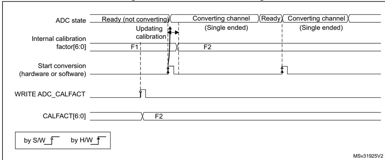
The timing diagram illustrates the process of forcing a calibration factor. It tracks several signals over time: - ADC state : Transitions from 'Ready (not converting)' to 'Converting channel (Single ended)' and back to 'Ready'. - Internal calibration factor[6:0] : Shows a value 'F1' being updated to 'F2' during a 'Ready' state when a write occurs. - Start conversion (hardware or software) : Shows pulses indicating the start of conversion cycles. - WRITE ADC_CALFACT : A software trigger pulse that initiates the update of the calibration factor. - CALFACT[6:0] : Shows the value 'F2' being latched. A legend at the bottom left distinguishes between software triggers (by S/W with a specific arrow symbol) and hardware triggers (by H/W with a different arrow symbol).
22.4.5 ADC on-off control (ADEN, ADDIS, ADRDY)
At power-up, the ADC is disabled and put in power-down mode (ADEN = 0).
As shown in Figure 83 , the ADC needs a stabilization time of \( t_{STAB} \) before it starts converting accurately.
Two control bits are used to enable or disable the ADC:
- • Set ADEN = 1 to enable the ADC. The ADRDY flag is set as soon as the ADC is ready for operation.
- • Set ADDIS = 1 to disable the ADC and put the ADC in Power-down. The ADEN and ADDIS bits are then automatically cleared by hardware as soon as the ADC is fully disabled.
Conversion can then start either by setting ADSTART to 1 (refer to Section 22.4.16: Conversion on external trigger and trigger polarity (EXTSEL, EXTEN) ) or when an external trigger event occurs if triggers are enabled.
Follow the procedure below to enable the ADC:
- 1. Clear the ADRDY bit in ADC_ISR register by programming this bit to 1.
- 2. Set ADEN = 1 in the ADC_CR register.
- 3. Wait until ADRDY = 1 in the ADC_ISR register (ADRDY is set after the ADC startup time). This can be handled by interrupt if the interrupt is enabled by setting the ADRDYIE bit in the ADC_IER register.
Follow the procedure below to disable the ADC:
- 1. Check that ADSTART = 0 in the ADC_CR register to ensure that no conversion is ongoing. If the software trigger mode was used, stop the software trigger mode by writing 1 to the ADSTP bit of the ADC_CR register and waiting until this bit is read at 0.
- 2. Set ADDIS = 1 in the ADC_CR register.
- 3. If required by the application, wait until ADEN = 0 in the ADC_CR register, indicating that the ADC is fully disabled (ADDIS is automatically reset once ADEN = 0).
- 4. Clear the ADRDY bit in ADC_ISR register by programming this bit to 1 (optional).
Figure 83. Enabling/disabling the ADC
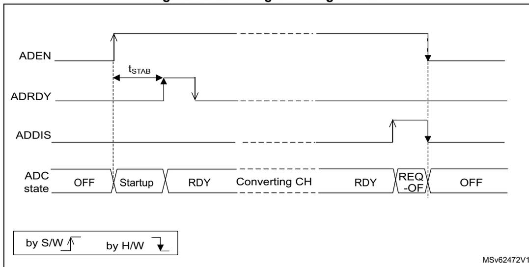
The diagram illustrates the timing for enabling and disabling the ADC. It shows four signal lines: ADEN, ADRDY, ADDIS, and ADC state. - ADEN is set high by software, triggering a startup phase. - After a stabilization time \( t_{STAB} \) , ADRDY is set high by hardware, and the ADC state becomes RDY. - During conversion, the state is "Converting CH". - To disable, ADDIS is set high by software. - This causes ADRDY to go low and the ADC state to transition through "REQ-OF" to "OFF". - ADEN and ADDIS are also reset to low by hardware at the end of the sequence. - A legend indicates that rising edges with an upward arrow are "by S/W" and falling edges with a downward arrow are "by H/W".
Note: In auto-off mode (AUTOFF = 1) the power-on/off phases are performed automatically, by hardware and the ADRDY flag is not set.
Caution: The ADEN bit cannot be set while the ADCAL bit is set, and during four ADC clock cycles after the ADCAL bit is cleared by the hardware (end of calibration).
22.4.6 ADC clock (PRESC[3:0])
The ADC has a dual clock-domain architecture, so that the ADC can be fed with a clock (ADC asynchronous clock) independent from the bus clock.
Figure 84. ADC clock scheme
![Figure 84. ADC clock scheme diagram showing the RCC (Reset and clock controller) connected to the AHB interface and the Analog ADC via adclk_hclk and adclk_ker_ck lines. The adclk_ker_ck line passes through a prescaler block with values /1, 2, 4, 6, 8, 10, 12, 16, 32, 64, 128, 256, controlled by Bits PRESC[3:0] of ADCx_CCR, resulting in FADC output to the Analog ADC.](/RM0521-STM32WBA2/31586fabab4387c18038dc901ca0e9cd_img.jpg)
The diagram illustrates the ADC clock scheme. On the left, the RCC (Reset and clock controller) is shown. It has two output lines: adclk_hclk and adclk_ker_ck. The adclk_hclk line connects to the AHB interface. The adclk_ker_ck line connects to a prescaler block. The prescaler block contains the values /1, 2, 4, 6, 8, 10, 12, 16, 32, 64, 128, 256. This block is controlled by Bits PRESC[3:0] of ADCx_CCR. The output of the prescaler is labeled FADC and connects to the Analog ADC. The entire ADC section (AHB interface, prescaler, and Analog ADC) is enclosed in a large box. A small label MSV62484V3 is at the bottom right of the box.
- 1. Refer to Section Reset and clock control (RCC) for how the bus clock and ADC asynchronous clock are enabled.
The adclk_ker_ck input clock can be selected between different clock sources (see Figure 84: ADC clock scheme ). This selection is done in the RCC (refer to the RCC section for more information):
- • The ADC clock can be provided by an internal or external clock source, which is independent and asynchronous with the bus clock.
- • The ADC clock can be derived from the bus clock by selecting the adclk_ker_ck as bus clock.
Option a) has the advantage of reaching the maximum ADC clock frequency whatever the clock scheme selected. The ADC clock can eventually be divided by a programmable ratio of 1, 2, 4, 6, 8, 10, 12, 16, 32, 64, 128 or 256, configured through PRESC[3:0] bits in the ADCx_CCR register.
Option b) has the advantage of bypassing the clock domain resynchronizations. This can be useful when the ADC is triggered by a timer and if the application requires that the ADC is precisely triggered without any uncertainty (otherwise, an uncertainty of the trigger instant is added by the resynchronizations between the two clock domains).
Table 168. Latency between trigger and start of conversion (1)
| ADC clock source | Latency between the trigger event and the start of conversion |
|---|---|
| Clock different from bus clock | Latency is not deterministic (jitter) |
| Bus clock divided by 2 | Latency is deterministic (no jitter) and equal to 4 ADC clock cycles |
| ADC clock source | Latency between the trigger event and the start of conversion |
|---|---|
| Bus clock divided by 4 | Latency is deterministic (no jitter) and equal to 3.75 ADC clock cycles |
| Bus clock divided by 1 | Latency is deterministic (no jitter) and equal to 4 ADC clock cycles |
1. Refer to the device datasheet for the maximum \( F_{ADC} \) frequency.
22.4.7 ADC connectivity
ADC inputs are connected to the external channels as well as internal sources as described in Figure 85.
Figure 85. ADC4 connectivity
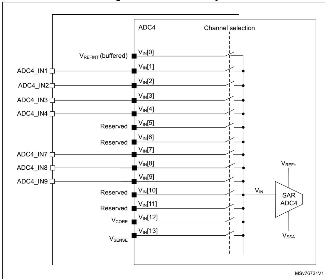
The diagram illustrates the connectivity of the ADC4 SAR (Successive Approximation Register) block. On the left, various internal and external sources are connected to the ADC4's input pins, labeled \( V_{IN}[0] \) through \( V_{IN}[13] \) . The connections are as follows:
- \( V_{REFINT} \) (buffered) is connected to \( V_{IN}[0] \) .
- External pins \( ADC4\_IN1 \) through \( ADC4\_IN9 \) are connected to \( V_{IN}[1] \) through \( V_{IN}[9] \) respectively.
- \( V_{IN}[5] \) and \( V_{IN}[6] \) are labeled as "Reserved".
- \( V_{IN}[10] \) and \( V_{IN}[11] \) are also labeled as "Reserved".
- \( V_{CORE} \) is connected to \( V_{IN}[12] \) .
- \( V_{SENSE} \) is connected to \( V_{IN}[13] \) .
Each input pin has a switch symbol that can connect it to a common bus. This bus is connected to the \( V_{IN} \) input of the SAR ADC4 block. The SAR ADC4 block also has \( V_{REF+} \) and \( V_{SSA} \) inputs. A dashed vertical line labeled "Channel selection" is positioned between the input pins and the common bus. The diagram is labeled MSV76721V1 in the bottom right corner.
22.4.8 Configuring the ADC
The software can write to the ADCAL and ADEN bits in the ADC_CR and ADC_PWR register if the ADC is disabled (ADEN must be 0).
The software must only write to the ADSTART and ADDIS bits in the ADC_CR register only if the ADC is enabled and there is no pending request to disable the ADC (ADEN = 1 and ADDIS = 0).
For all the other control bits in the ADC_IER, ADC_CFGRI, ADC_SMPR, ADC_CHSELR and ADC_CCR registers, refer to the description of the corresponding control bit in Section 22.7: ADC registers . If the ADC operates in software trigger mode, set the ADSTP bit in ADC_CR register, then wait until ADSTP bit become 0 before reconfiguring the above registers.
ADC_AWDTRi registers can be modified when a conversion is ongoing.
The software must only write to the ADSTP bit in the ADC_CR register if the ADC is enabled (and possibly converting) and there is no pending request to disable the ADC (ADSTART = 1 and ADDIS = 0).
Note: There is no hardware protection preventing software from making write operations forbidden by the above rules. If such a forbidden write access occurs, the ADC may enter an undefined state. To recover correct operation in this case, the ADC must be disabled (clear ADEN = 0 and all the bits in the ADC_CR register).
22.4.9 Channel selection (CHSEL, SCANDIR, CHSELROMOD)
There are up to 10 multiplexed channels:
- • 7 analog inputs from GPIO pins (ADC_INx)
- • 3 internal analog inputs: temperature Sensor, internal reference voltage, V CORE
It is possible to convert a single channel or a sequence of channels.
The sequence of the channels to be converted can be programmed in the ADC_CHSELR channel selection register: each analog input channel has a dedicated selection bit (CHSELx).
The ADC scan sequencer can be used in two different modes:
- • Sequencer not fully configurable:
The order in which the channels are scanned is defined by the channel number (CHSELROMOD bit must be cleared in ADC_CFGR1 register):- – Sequence length configured through CHSELx bits in ADC_CHSELR register
- – Sequence direction: the channels are scanned in a forward direction (from the lowest to the highest channel number) or backward direction (from the highest to the lowest channel number) depending on the value of SCANDIR bit (SCANDIR = 0: forward scan, SCANDIR = 1: backward scan)
- – Any channel can belong to in these sequences
- • Fully-configurable sequencer
The CHSELRMOD bit is set in ADC_CFGR1 register.- – Sequencer length is up to eight channels
- – The order in which the channels are scanned is independent from the channel number. Any order can be configured through SQ1[3:0] to SQ8[3:0] bits in ADC_CHSELR register.
- – If the sequencer detects SQx[3:0] = 0b1111, the following SQx[3:0] registers are ignored.
- – If no 0b1111 is programmed in SQx[3:0], the sequencer scans full eight channels.
The software is allowed to program the CHSEL, SCANDIR and CHSELRMOD bit only when ADSTART bit is cleared in ADC_CR register. This ensures that no conversion is ongoing. If the ADC operated in software trigger mode, set ADSTP bit then wait until ADSTP bit become 0 before reconfiguring these registers. This sequence must be respected even if ADSTART bit is cleared to 0 after the conversion,
Temperature sensor, V REFINT , and V CORE internal channels
The temperature sensor, the internal reference voltage (V REFINT ), and V CORE are connected to ADC internal channels. Refer to Table ADC interconnection in Section 22.4.2: ADC pins and internal signals for details.
22.4.10 Programmable sampling time (SMPx[2:0])
Before starting a conversion, the ADC needs to establish a direct connection between the voltage source to be measured and the embedded sampling capacitor of the ADC. This sampling time must be enough for the input voltage source to charge the sample and hold capacitor to the input voltage level.
Having a programmable sampling time allows the conversion speed to be trimmed according to the input resistance of the input voltage source.
The ADC samples the input voltage for a number of ADC clock cycles that can be modified using the SMP1[2:0] and SMP2[2:0] bits in the ADC_SMPR register.
Each channel can choose one out of two sampling times configured in SMP1[2:0] and SMP2[2:0] bitfields, through SMPSELx bits in ADC_SMPR register.
The total conversion time is calculated as follows:
Example:
With ADC_CLK = 16 MHz and a sampling time of 1.5 ADC clock cycles:
The ADC indicates the end of the sampling phase by setting the EOSMP flag.
I/O analog switch voltage booster
The resistance of the I/O analog switch increases when the V DDA voltage is too low. The sampling time must consequently be adapted accordingly (refer to the device datasheet for the corresponding electrical characteristics). This resistance can be minimized at low V DDA voltage by enabling an internal voltage booster through the BOOSTEN bit of the
SYSCFG_CFGR1 register or by selecting a \( V_{DD} \) booster voltage through the ANASWVDD bit of the SYSCFG_CFGR1 register.
22.4.11 Single conversion mode (CONT = 0)
In single conversion mode, the ADC performs a single sequence of conversions, converting all the channels once. This mode is selected when CONT is cleared in the ADC_CFGR1 register. Conversion is started by either:
- • Setting the ADSTART bit in the ADC_CR register
- • Hardware trigger event
Inside the sequence, after each conversion is complete:
- • The converted data are stored in the 16-bit ADC_DR register
- • The EOC (end of conversion) flag is set
- • An interrupt is generated if the EOCIE bit is set
After the sequence of conversions is complete:
- • The EOS (end of sequence) flag is set
- • An interrupt is generated if the EOSIE bit is set
Then the ADC stops until a new external trigger event occurs or the ADSTART bit is set again.
Note: To convert a single channel, program a sequence with a length of 1.
22.4.12 Continuous conversion mode (CONT = 1)
In continuous conversion mode, when a software or hardware trigger event occurs, the ADC performs a sequence of conversions, converting all the channels once and then automatically re-starts and continuously performs the same sequence of conversions. This mode is selected when CONT is set to 1 in the ADC_CFGR1 register. Conversion is started by either:
- • Setting the ADSTART bit in the ADC_CR register
- • Hardware trigger event
Inside the sequence, after each conversion is complete:
- • The converted data are stored in the 16-bit ADC_DR register
- • The EOC (end of conversion) flag is set
- • An interrupt is generated if the EOCIE bit is set
After the sequence of conversions is complete:
- • The EOS (end of sequence) flag is set
- • An interrupt is generated if the EOSIE bit is set
Then, a new sequence restarts immediately and the ADC continuously repeats the conversion sequence.
Note: To convert a single channel, program a sequence with a length of 1.
It is not possible to have both discontinuous mode and continuous mode enabled: it is forbidden to set both bits DISCEN = 1 and CONT = 1.
22.4.13 Starting conversions (ADSTART)
Software starts ADC conversions by setting ADSTART to 1.
When ADSTART is set, the conversion:
- • Starts immediately if EXTEN = 00 (software trigger)
- • At the next active edge of the selected hardware trigger if EXTEN ≠ 00
The ADSTART bit is also used to indicate whether an ADC operation is currently ongoing. It is possible to re-configure the ADC while ADSTART remains at 0, indicating that the ADC is idle.
The ADSTART bit is cleared by hardware:
- • In single mode with software trigger (CONT = 0, EXTEN = 00)
- – At any end of conversion sequence (EOS = 1)
- • In discontinuous mode with software trigger (CONT = 0, DISCEN = 1, EXTEN = 00)
- – At end of conversion (EOC = 1)
- • In all cases (CONT = x, EXTEN = XX)
- – After execution of the ADSTP procedure invoked by software (see Section 22.4.15: Stopping an ongoing conversion (ADSTP) ).
When the ADC operates in autonomous mode (DPD bit transition from 1 to 0, see Autonomous mode (AUTOFF, DPD) ), the ADSTART bit can be set only when the ADC is powered on. (both LDORDY = 1 and ADRDY = 1). In continuous mode (CONT = 1), the ADSTART bit is not cleared by hardware when the EOS flag is set because the sequence is automatically relaunched.
Note: When hardware trigger is selected in single mode (CONT = 0 and EXTEN = 01), ADSTART is not cleared by hardware when the EOS flag is set. This avoids the need for software having to set the ADSTART bit again and ensures the next trigger event is not missed. It is necessary to set ADSTP to 1 and wait until ADSTP is cleared before reconfiguring or disabling the ADC, even if ADSTART bit is cleared to after the software triggered ADC conversion mode.
22.4.14 Timings
The elapsed time between the start of a conversion and the end of conversion is the sum of the configured sampling time plus the successive approximation time depending on data resolution:
Figure 86. Analog-to-digital conversion time
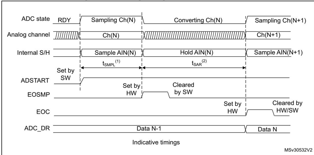
The diagram shows the timing of an ADC conversion. The 'ADC state' line transitions from 'RDY' to 'Sampling Ch(N)', then 'Converting Ch(N)', and finally 'Sampling Ch(N+1)'. The 'Analog channel' line shows 'Ch(N)' being sampled and then 'Ch(N+1)'. The 'Internal S/H' line shows 'Sample AIN(N)', 'Hold AIN(N)', and 'Sample AIN(N+1)'. The 'ADSTART' signal is set by software (SW) at the beginning of the sampling phase. The 'EOSMP' signal is set by hardware (HW) at the start of the conversion phase and cleared by SW. The 'EOC' signal is set by HW at the end of the conversion phase and cleared by HW/SW. The 'ADC_DR' register contains 'Data N-1' during the conversion of 'Ch(N)' and 'Data N' during the sampling of 'Ch(N+1)'. The sampling time is labeled \( t_{SMPL}^{(1)} \) and the conversion time is labeled \( t_{SAR}^{(2)} \) . The diagram is labeled 'Indicative timings' and 'MSV30532V2'.
- 1. \( t_{SMPL} \) depends on SMP[2:0].
- 2. \( t_{SAR} \) depends on RES[2:0].
Figure 87. ADC conversion timings
The diagram shows the timing of ADC conversions. The 'ADSTART' signal is triggered, and the 'ADC state' transitions from 'Ready' to 'S0', then 'Conversion 0', 'S1', 'Conversion 1', 'S2', 'Conversion 2', 'S3', and 'Conversion 3'. The 'ADC_DR' register is updated with 'Data 0', 'Data 1', and 'Data 2'. The latency from the ADSTART trigger to the start of the first conversion is labeled \( t_{LATENCY}^{(2)} \) . The write latency for the ADC_DR register is labeled \( W_{LATENCY}^{(3)} \) . The diagram is labeled 'MSV33174V1'.
- 1. EXTEN = 00 or EXTEN ≠ 00.
- 2. Trigger latency (refer to datasheet for more details).
- 3. ADC_DR register write latency (refer to datasheet for more details).
22.4.15 Stopping an ongoing conversion (ADSTP)
The software can decide to stop any ongoing conversions by setting ADSTP to 1 in the ADC_CR register.
This resets the ADC operation and the ADC is idle, ready for a new operation.
When the ADSTP bit is set by software, any ongoing conversion is aborted and the result is discarded (ADC_DR register is not updated with the current conversion).
The scan sequence is also aborted and reset (meaning that restarting the ADC would re-start a new sequence).
Once this procedure is complete, the ADSTP and ADSTART bits are both cleared by hardware and the software must wait until ADSTART is cleared to 0 before starting new conversions.
Figure 88. Stopping an ongoing conversion
The diagram illustrates the timing for stopping an ongoing conversion. The ADC state transitions from RDY to SAMPLING CH(N) to CONVERTING CH(N) and back to RDY. The ADSTART bit is set by software (SW) to start the conversion and is cleared by hardware (HW) when the conversion is complete. The ADSTOP bit is set by software to abort an ongoing conversion and is cleared by hardware. The ADC_DR register contains DATA N-1 during the conversion. A vertical dashed line indicates the point where ADSTOP is set, which causes the conversion to be aborted and the ADC to return to the RDY state.
22.4.16 Conversion on external trigger and trigger polarity (EXTSEL, EXTEN)
A conversion or a sequence of conversion can be triggered either by software or by an external event (for example timer capture). If the EXTEN[1:0] control bits are not equal to “0b00”, then external events are able to trigger a conversion with the selected polarity. The trigger selection is effective once software has set bit ADSTART to 1.
Any hardware triggers which occur while a conversion is ongoing are ignored.
If bit ADSTART is cleared, any hardware triggers which occur are ignored.
Table 169 provides the correspondence between the EXTEN[1:0] values and the trigger polarity.
Table 169. Configuring the trigger polarity
| Source | EXTEN[1:0] |
|---|---|
| Trigger detection disabled | 00 |
| Detection on rising edge | 01 |
| Detection on falling edge | 10 |
| Detection on both rising and falling edges | 11 |
Note: The polarity of the external trigger can be changed only when the ADC is not converting (ADSTART = 0).
The EXTSEL[2:0] control bits are used to select which of 8 possible events can trigger conversions.
Refer to Table ADC interconnection in Section 22.4.2: ADC pins and internal signals for the list of all the external triggers that can be used for regular conversion.
The software source trigger events can be generated by setting the ADSTART bit in the ADC_CR register.
Note: The trigger selection can be changed only when the ADC is not converting (ADSTART = 0).
22.4.17 Discontinuous mode (DISCEN)
This mode is enabled by setting the DISCEN bit in the ADC_CFGR1 register.
In this mode (DISCEN = 1), a hardware or software trigger event is required to start each conversion defined in the sequence. On the contrary, if DISCEN is cleared, a single hardware or software trigger event successively starts all the conversions defined in the sequence.
Example:
- • DISCEN = 1, channels to be converted are channels 0, 3, 7 and 10
- – 1st trigger: channel 0 is converted and an EOC event is generated
- – 2nd trigger: channel 3 is converted and an EOC event is generated
- – 3rd trigger: channel 7 is converted and an EOC event is generated
- – 4th trigger: channel 10 is converted and both EOC and EOS events are generated.
- – 5th trigger: channel 0 is converted an EOC event is generated
- – 6th trigger: channel 3 is converted and an EOC event is generated
- – ...
- • DISCEN = 0, channels to be converted are channels 0, 3, 7 and 10
- – 1st trigger: the complete sequence is converted: channel 0, then 3, 7 and 10. Each conversion generates an EOC event and the last one also generates an EOS event.
- – Any subsequent trigger events restarts the complete sequence.
Note: It is not possible to have both discontinuous mode and continuous mode enabled: it is forbidden to set both bits DISCEN = 1 and CONT = 1.
22.4.18 Programmable resolution (RES) - fast conversion mode
It is possible to obtain faster conversion times ( \( t_{SAR} \) ) by reducing the ADC resolution.
The resolution can be configured to be either 12, 10, 8, or 6 bits by programming the RES[1:0] bits in the ADC_CFGR1 register. Lower resolution allows faster conversion times for applications where high data precision is not required.
Note: The RES[1:0] bit must only be changed when the ADEN bit is reset.
The result of the conversion is always 12 bits wide and any unused LSB bits are read as zeros.
Lower resolution reduces the conversion time needed for the successive approximation steps as shown in Table 170 .
Table 170. \( t_{SAR} \) timings depending on resolution
| RES[1:0] bits | \( t_{SAR} \) (ADC clock cycles) | \( t_{SAR} \) (ns) at \( f_{ADC} = 35 \) MHz | \( t_{SMPL} \) (min) (ADC clock cycles) | \( t_{CONV} \) (ADC clock cycles) (with min. \( t_{SMPL} \) ) | \( t_{CONV} \) (ns) at \( f_{ADC} = 35 \) MHz |
|---|---|---|---|---|---|
| 12 | 12.5 | 357 | 1.5 | 14 | 400 |
| 10 | 10.5 | 300 | 1.5 | 12 | 343 |
| 8 | 8.5 | 243 | 1.5 | 10 | 286 |
| 6 | 6.5 | 186 | 1.5 | 8 | 229 |
22.4.19 End of conversion, end of sampling phase (EOC, EOSMP flags)
The ADC indicates each end of conversion (EOC) event.
The ADC sets the EOC flag in the ADC_ISR register as soon as a new conversion data result is available in the ADC_DR register. An interrupt can be generated if the EOCIE bit is set in the ADC_IER register. The EOC flag is cleared by software either by writing 1 to it, or by reading the ADC_DR register.
The ADC also indicates the end of sampling phase by setting the EOSMP flag in the ADC_ISR register. The EOSMP flag is cleared by software by writing 1 to it. An interrupt can be generated if the EOSMPIE bit is set in the ADC_IER register.
The aim of this interrupt is to allow the processing to be synchronized with the conversions. Typically, an analog multiplexer can be accessed in hidden time during the conversion phase, so that the multiplexer is positioned when the next sampling starts.
Note: As there is only a very short time left between the end of the sampling and the end of the conversion, it is recommended to use polling or a WFE instruction rather than an interrupt and a WFI instruction.
22.4.20 End of conversion sequence (EOS flag)
The ADC notifies the application of each end of sequence (EOS) event.
The ADC sets the EOS flag in the ADC_ISR register as soon as the last data result of a conversion sequence is available in the ADC_DR register. An interrupt can be generated if the EOSIE bit is set in the ADC_IER register. The EOS flag is cleared by software by writing 1 to it.
22.4.21 Example timing diagrams (single/continuous modes hardware/software triggers)
Figure 89. Single conversions of a sequence, software trigger
The timing diagram shows the following signals and their states over time:
- ADSTART (1) : Software (SW) and Hardware (HW) triggers. The diagram shows two sequences initiated by SW and HW triggers.
- EOC : End of Conversion pulses. Each pulse corresponds to the completion of a channel conversion.
- EOS : End of Sequence flag. It is set after the last conversion in the sequence.
- SCANDIR : Scan direction indicator. It is set when the sequence is active.
- ADC state (2) : The state of the ADC during the sequence. The sequence of states is: RDY, CH0, CH9, CH10, CH17, RDY, CH17, CH10, CH9, CH0, RDY.
- ADC_DR : Data Register. The data values corresponding to the states are: D0, D9, D10, D17, D17, D10, D9, D0.
Legend:
by S/W by H/W
MSV30338V3
- 1. EXTEN = 00, CONT = 0.
- 2. CHSEL = 0x20601, WAIT = 0, AUTOFF = 0.
Figure 90. Continuous conversion of a sequence, software trigger
by S/W by H/W
MSv30339V2
- 1. EXTEN = 00, CONT = 1.
- 2. CHSEL = 0x20601, WAIT = 0, AUTOFF = 0.
Figure 91. Single conversions of a sequence, hardware trigger
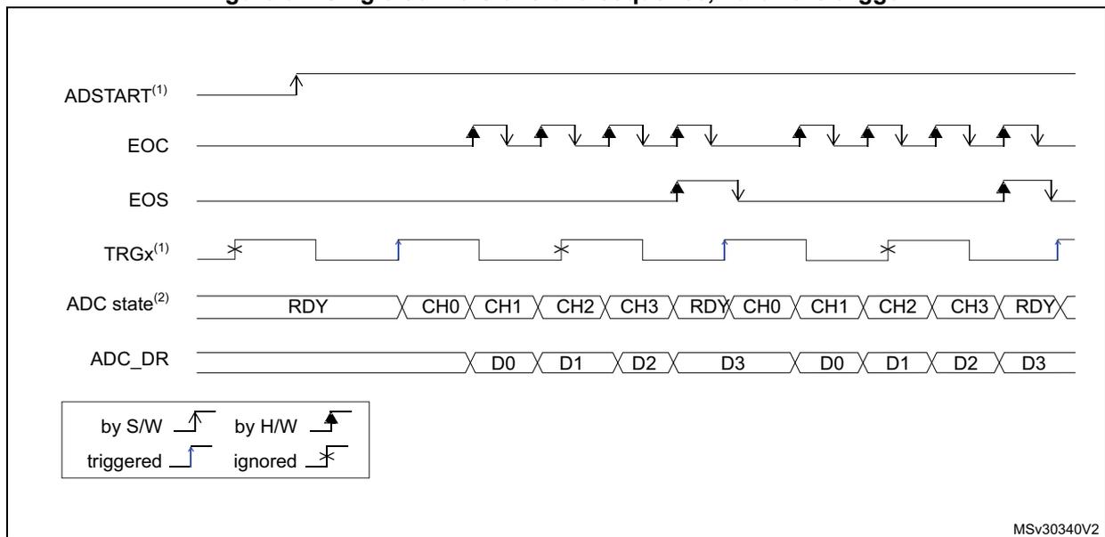
by S/W by H/W
triggered ignored
MSv30340V2
- 1. EXTSEL = TRGx (over-frequency), EXTEN = 01 (rising edge), CONT = 0.
- 2. CHSEL = 0xF, SCANDIR = 0, WAIT = 0, AUTOFF = 0.
Figure 92. Continuous conversions of a sequence, hardware trigger
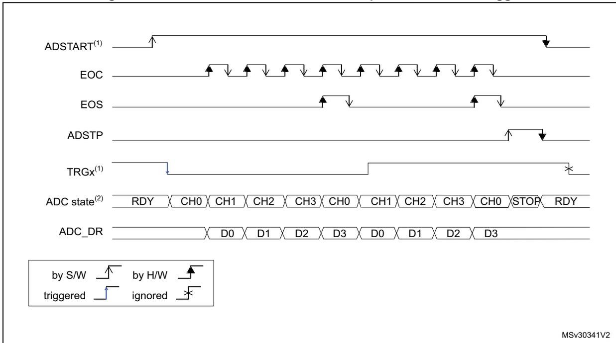
The diagram illustrates the timing for continuous conversions.
-
ADSTART
(1)
: A software (S/W) rising edge starts the conversion sequence.
-
EOC
: A series of hardware (H/W) rising and falling edges indicating the end of each conversion.
-
EOS
: Hardware (H/W) rising and falling edges indicating the end of the sequence.
-
ADSTP
: A software (S/W) rising edge stops the sequence.
-
TRGx
(1)
: A hardware (H/W) falling edge triggers the start of conversions.
-
ADC state
(2)
: Shows the sequence of conversions: RDY → CH0 → CH1 → CH2 → CH3 → CH0 → CH1 → CH2 → CH3 → CH0 → STOP → RDY.
-
ADC_DR
: Shows the data register values: D0 → D1 → D2 → D3 → D0 → D1 → D2 → D3.
-
Legend
:
- by S/W: solid line arrow, triggered (rising edge).
- by H/W: dashed line arrow, ignored (falling edge).
MSv30341V2
- 1. EXTSEL = TRGx, EXTEN = 10 (falling edge), CONT = 1.
- 2. CHSEL = 0xF, SCANDIR = 0, WAIT = 0, AUTOFF = 0.
22.4.22 Low-frequency trigger mode
If the application has to support a time longer than the maximum \( t_{\text{IDLE}} \) value (between one trigger to another for single conversion mode or between the ADC enable and the first ADC conversion), then the ADC internal state needs to be rearmed. This mechanism can be enabled by setting LFTRIG bit to 1 in ADC_CFGR2 register. By setting this bit, any trigger (software or hardware) sends a rearm command to ADC. The conversion is started after a two ADC clock cycle delay compared to LFTRIG set to 0.
It is not necessary to use this mode when AUTOFF bit is set to 1. For wait mode, only the first trigger generates an internal rearm command.
22.4.23 Data management
Data register and data alignment (ADC_DR, ALIGN)
At the end of each conversion (when an EOC event occurs), the result of the converted data is stored in the ADC_DR data register which is 16-bit wide.
The format of the ADC_DR depends on the configured data alignment and resolution.
The ALIGN bit in the ADC_CFGR1 register selects the alignment of the data stored after conversion. Data can be right-aligned (ALIGN = 0) or left-aligned (ALIGN = 1) as shown in Figure 93.
Figure 93. Data alignment and resolution (oversampling disabled: OVSE = 0)
| ALIGN | RES | 15 | 14 | 13 | 12 | 11 | 10 | 9 | 8 | 7 | 6 | 5 | 4 | 3 | 2 | 1 | 0 |
|---|---|---|---|---|---|---|---|---|---|---|---|---|---|---|---|---|---|
| 0 | 0x0 | 0x0 DR[11:0] | |||||||||||||||
| 0x1 | 0x00 DR[9:0] | ||||||||||||||||
| 0x2 | 0x00 DR[7:0] | ||||||||||||||||
| 0x3 | 0x00 DR[5:0] | ||||||||||||||||
| 1 | 0x0 | DR[11:0] | 0x0 | ||||||||||||||
| 0x1 | DR[9:0] | 0x00 | |||||||||||||||
| 0x2 | DR[7:0] | 0x00 | |||||||||||||||
| 0x3 | 0x00 DR[5:0] | 0x0 | |||||||||||||||
MS30342V1
ADC overrun (OVR, OVRMOD)
The overrun flag (OVR) indicates a data overrun event, when the converted data was not read in time by the CPU or the DMA, before the data from a new conversion is available.
The OVR flag is set in the ADC_ISR register if the EOC flag is still at 1 at the time when a new conversion completes. An interrupt can be generated if the OVRRIE bit is set in the ADC_IER register.
When an overrun condition occurs, the ADC keeps operating and can continue to convert unless the software decides to stop and reset the sequence by setting the ADSTP bit in the ADC_CR register.
The OVR flag is cleared by software by writing 1 to it.
It is possible to configure if the data is preserved or overwritten when an overrun event occurs by programming the OVRMOD bit in the ADC_CFGR1 register:
- • OVRMOD = 0
- – An overrun event preserves the data register from being overwritten: the old data is maintained and the new conversion is discarded. If OVR remains at 1, further conversions can be performed but the resulting data is discarded.
- • OVRMOD = 1
- – The data register is overwritten with the last conversion result and the previous unread data is lost. If OVR remains at 1, further conversions can be performed and the ADC_DR register always contains the data from the latest conversion.
Figure 94. Example of overrun (OVR)
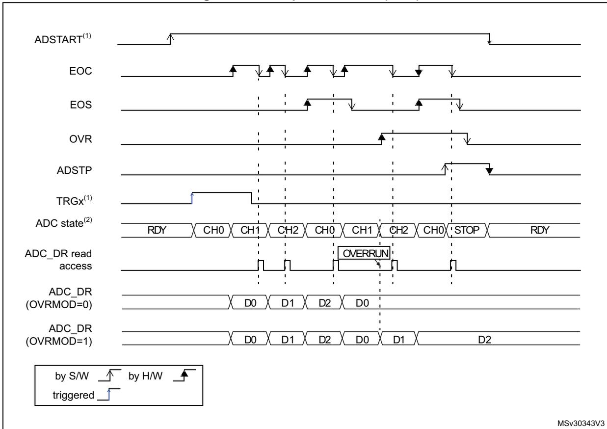
The diagram shows the following signals and states over time:
- ADSTART (1) : A software trigger that starts the ADC sequence.
- EOC : End of Conversion flag, toggling for each channel conversion.
- EOS : End of Sequence flag, toggling at the end of each sequence.
- OVR : Overrun flag, set when a new conversion starts before the previous data is read.
- ADSTP : Stop conversion flag.
- TRGx (1) : Hardware trigger signal.
- ADC state (2) : Sequence of states: RDY, CH0, CH1, CH2, CH0, CH1, CH2, CH0, STOP, RDY.
- ADC_DR read access : Software reads of the data register. An 'OVERRUN' is indicated when a read is missed.
- ADC_DR (OVRMOD=0) : Data register contents when overrun mode is disabled: D0, D1, D2, D0.
- ADC_DR (OVRMOD=1) : Data register contents when overrun mode is enabled: D0, D1, D2, D0, D1, D2.
Legend for signal transitions:
- by S/W (Software): rising edge
- by H/W (Hardware): falling edge
- triggered: rising edge
MSv30343V3
Managing a sequence of data converted without using the DMA
If the conversions are slow enough, the conversion sequence can be handled by software. In this case the software must use the EOC flag and its associated interrupt to handle each data result. Each time a conversion is complete, the EOC bit is set in the ADC_ISR register and the ADC_DR register can be read. The OVRMOD bit in the ADC_CFGR1 register must be configured to 0 to manage overrun events as an error.
Managing converted data without using the DMA without overrun
It may be useful to let the ADC convert one or more channels without reading the data after each conversion. In this case, the OVRMOD bit must be configured at 1 and the OVR flag must be ignored by the software. When OVRMOD is set to 1, an overrun event does not prevent the ADC from continuing to convert and the ADC_DR register always contains the latest conversion data.
Managing converted data using the DMA
Since all converted channel values are stored in a single data register, it is efficient to use DMA when converting more than one channel. This avoids losing the conversion data results stored in the ADC_DR register.
When DMA mode is enabled (DMAEN bit set to 1 in the ADC_CFGR1 register), a DMA request is generated after the conversion of each channel. This allows the transfer of the
converted data from the ADC_DR register to the destination location selected by the software.
Note: The DMAEN bit in the ADC_CFGR1 register must be set after the ADC calibration phase.
Despite this, if an overrun occurs (OVR = 1) because the DMA did not serve the DMA transfer request in time, the ADC stops generating DMA requests and the data corresponding to the new conversion is not transferred by the DMA. Which means that all the data transferred to the RAM can be considered as valid.
Depending on the configuration of OVRMOD bit, the data is either preserved or overwritten (refer to ADC overrun (OVR, OVRMOD) ).
The DMA transfer requests are blocked until the software clears the OVR bit.
Two different DMA modes are proposed depending on the application use and are configured with bit DMACFG in the ADC_CFGR1 register:
- • DMA one-shot mode (DMACFG = 0).
This mode must be selected when the DMA is programmed to transfer a fixed number of data words. - • DMA circular mode (DMACFG = 1)
This mode must be selected when programming the DMA in circular mode or double buffer mode.
DMA one-shot mode (DMACFG = 0)
In this mode, the ADC generates a DMA transfer request each time a new conversion data word is available and stops generating DMA requests once the DMA has reached the last DMA transfer (when a transfer complete interrupt occurs - refer to DMA section), even if a conversion has been started again.
When the DMA transfer is complete (all the transfers configured in the DMA controller have been done):
- • The content of the ADC data register is frozen.
- • Any ongoing conversion is aborted and its partial result discarded
- • No new DMA request is issued to the DMA controller. This avoids generating an overrun error if there are still conversions which are started.
- • The scan sequence is stopped and reset
- • The DMA is stopped
DMA circular mode (DMACFG = 1)
In this mode, the ADC generates a DMA transfer request each time a new conversion data word is available in the data register, even if the DMA has reached the last DMA transfer. This allows the DMA configuration in circular mode in order to handle a continuous analog input data stream.
22.4.24 Low-power features
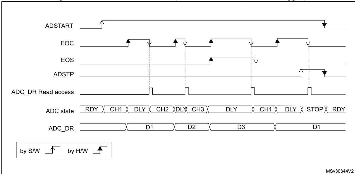
Wait conversion mode (WAIT)
Wait conversion mode can be used to simplify the software as well as optimizing the performance of applications clocked at low frequency where there might be a risk of ADC overrun occurring.
When the WAIT bit is set to 1 in the ADC_CFGR1 register, a new conversion can start only if the previous data has been treated, once the ADC_DR register has been read or if the EOC bit has been cleared.
This is a way to automatically adapt the speed of the ADC to the speed of the system that reads the data.
Note: Any hardware triggers which occur while a conversion is ongoing or during the wait time preceding the read access are ignored.
Figure 95. Wait conversion mode (continuous mode, software trigger)
MSV30344V2
- 1. EXTEN = 00, CONT = 1.
- 2. CHSEL = 0x3, SCANDIR = 0, WAIT = 1, AUTOFF = 0.
ADC power-saving modes
The ADC embeds two power-saving modes, the auto-off and the autonomous modes.
Auto-off mode (AUTOFF)
The auto-off mode is enabled by setting the AUTOFF bit to 1 in the ADC_PWRR register.
Below the auto-off mode operating sequence:
- 1. When AUTOFF is set to 1, the ADC is always powered off when no conversion is ongoing.
- 2. It then automatically wakes up when a conversion is triggered by software or by hardware, and a startup time is inserted between the trigger event and the ADC sampling time.
- 3. The ADC is then automatically disabled once the conversion or sequence of conversions is complete.
- 4. When consecutive hardware or software triggers occur, the ADC is automatically enabled and the conversion is processed.
Refer to Figure 96 for a description of auto-off mode state diagram.
The auto-off mode dramatically reduces power consumption in applications requiring a limited number of conversions or conversion requests far between enough (for example with a low-frequency hardware trigger) to justify the extra power and time used for switching the ADC on and off.
Auto-off mode can be combined with wait mode (WAIT = 1) for applications clocked at low frequency. This combination can achieve significant power saving if the ADC is automatically powered off during the wait phase and restarted as soon as the ADC_DR register is read by the application (see Figure 97: ADC behavior with WAIT = 0 and AUTOFF = 1 and Figure 98: ADC behavior with WAIT = 1 and AUTOFF = 1 ).
The auto-off mode is compatible with the autonomous peripheral mode.
Note: Refer to the Section Reset and clock control (RCC) for the description of how to manage the dedicated internal oscillators. The ADC interface can automatically switch on/off these internal oscillators to save power.
Figure 96. Auto-off mode state diagram
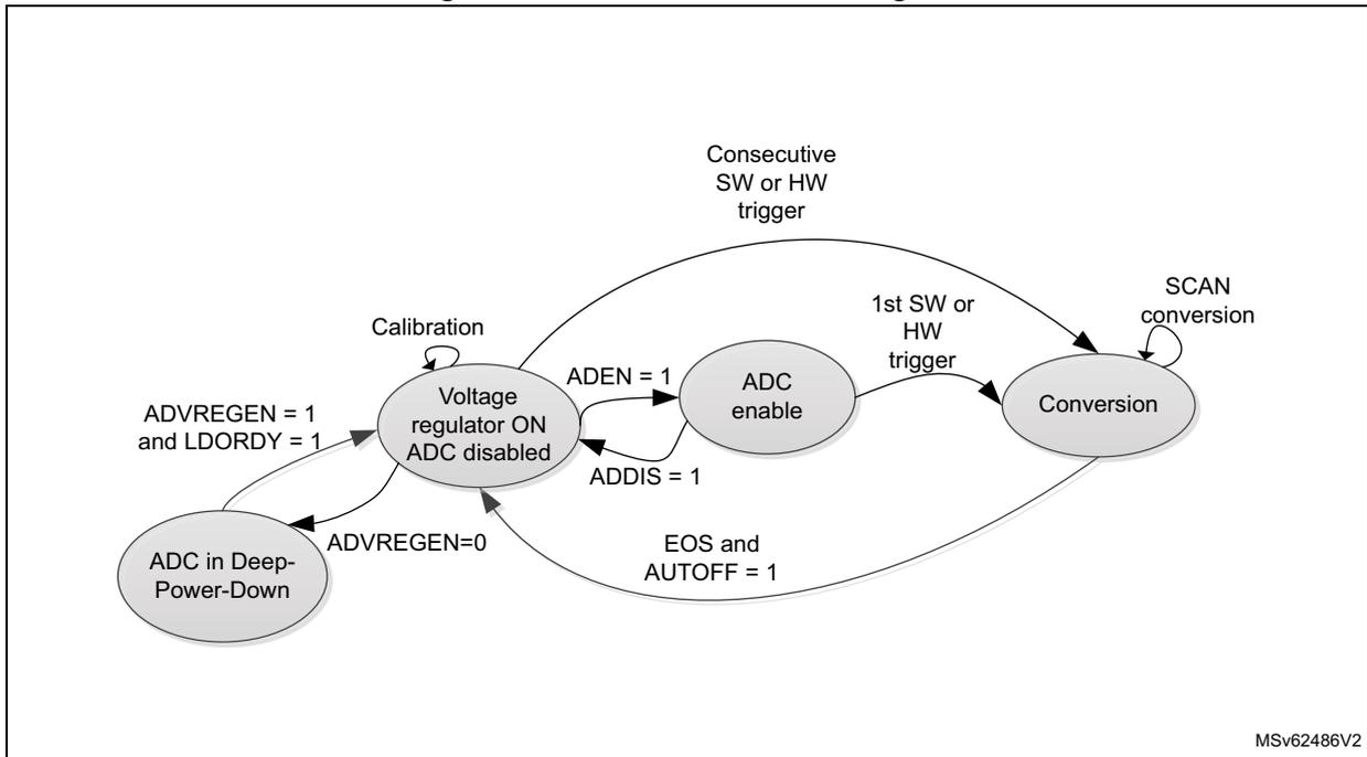
stateDiagram-v2
    State1: ADC in Deep-Power-Down
    State2: Voltage regulator ON ADC disabled
    State3: ADC enable
    State4: Conversion

    State1 --> State2: ADVREGEN = 1 and LDORDY = 1
    State2 --> State1: ADVREGEN=0
    State2 --> State2: Calibration
    State2 --> State3: ADEN = 1
    State3 --> State2: ADDIS = 1
    State3 --> State4: 1st SW or HW trigger
    State4 --> State4: SCAN conversion
    State4 --> State2: EOS and AUTOFF = 1
    State4 --> State2: Consecutive SW or HW trigger
MSv62486V2
Figure 97. ADC behavior with WAIT = 0 and AUTOFF = 1
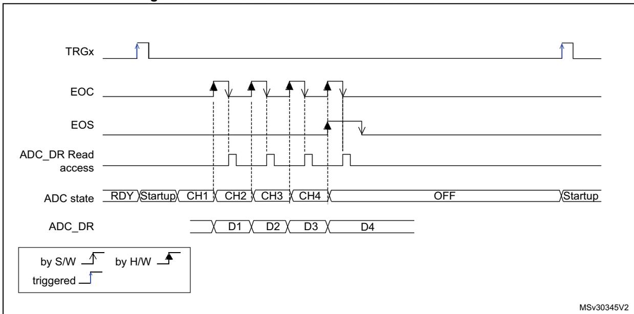
by S/W by H/W
triggered
MSv30345V2
- EXTSEL = TRGx, EXTEN = 01 (rising edge), CONT = x, ADSTART = 1, CHSEL = 0xF, SCANDIR = 0, WAIT = 0, AUTOFF = 1.
Figure 98. ADC behavior with WAIT = 1 and AUTOFF = 1
The diagram shows the following signals and states over time:
- TRGx: Hardware trigger signal. Rising edges are labeled 'by H/W triggered'.
- EOC: End of Conversion signal. It pulses high when a conversion is complete.
- EOS: End of Sequence signal. It pulses high when the end of a conversion sequence is reached.
- ADC_DR Read access: Signal indicating when the ADC data register is being read.
- ADC state: Shows the state of the ADC: RDY (Ready), Startup, CH1 (Channel 1), OFF, Startup, CH2, OFF, Startup, CH3, OFF, Startup, CH1, OFF, CH2. The 'DLY' (Delay) period is indicated between the Startup state and the start of conversion.
- ADC_DR: Data Register values: D1, D2, D3, D4.
Legend:
- by S/W triggered: Software trigger (rising edge).
- by H/W triggered: Hardware trigger (rising edge).
MSv30346V2
- 1. EXTSEL = TRGx, EXTEN = 01 (rising edge), CONT = x, ADSTART = 1, CHSEL = 0xF, SCANDIR = 0, WAIT = 1, AUTOFF = 1.
Autonomous mode (AUTOFF, DPD)
The autonomous mode is enabled by setting both AUTOFF and DPD bits to 1 in ADC_PWR register. In addition, the autonomous mode must be enabled in the RCC.
Below the autonomous mode operating sequence:
- 1. When AUTOFF and DPD are both set to 1, the ADC is powered off when no conversion is ongoing.
- 2. Upon hardware trigger reception, the ADC requests the adc_ker_ck and adc_hclk clocks to the RCC, the ADC voltage regulator is enabled, the calibration factor is loaded, the ADC is enabled and the conversion starts.
- 3. Once the ADC conversion is complete, the ADC can either generate an AWDx interrupt or a DMA request, depending on peripheral configuration:
- – When DMA mode is enabled, the ADC generates a DMA request to transfer data to memory or to another peripherals.
- – When an analog watchdog is enabled, ADC data do not need to be transferred. The analog watchdog compares the data to the threshold value and generates an AWDx interrupt to wake up the device if the data is under or over the programmed threshold.
- 4. When the ADC conversion/sequence or conversion is complete, the ADC and the ADC voltage regulator are automatically disabled as well as \( V_{REFINT} \) buffer and the temperature sensor, and further clock requests are deasserted. This allows the minimization of current consumption.
- 5. When consecutive hardware triggers occur, the ADC is automatically enabled and the conversion is processed.
Refer to Figure 99 for a description of autonomous mode state diagram.
The autonomous mode enables the ADC peripheral to operate when the device is in Stop mode. However it can also be used in Run or Sleep mode.
It is compatible with the autonomous peripheral mode.
Figure 99. Autonomous mode state diagram
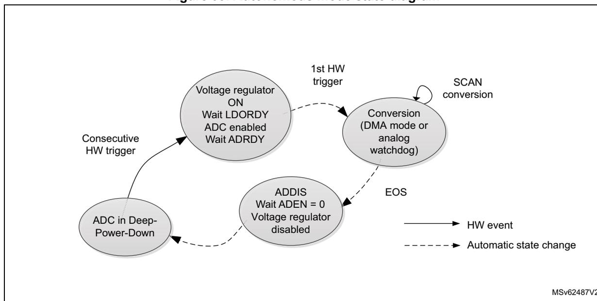
stateDiagram-v2
    [*] --> ADC_in_Deep_Power_Down: Consecutive HW trigger
    ADC_in_Deep_Power_Down --> Voltage_regulator_ON: ADDIS Wait ADEN = 0 Voltage regulator disabled
    Voltage_regulator_ON --> Conversion: 1st HW trigger
    Conversion --> Voltage_regulator_ON: SCAN conversion
    Conversion --> ADDIS: EOS
Legend:
- ———— HW event
- - - - - Automatic state change
MSv62487V2
22.4.25 Analog window watchdog
The three AWD analog watchdogs monitor whether some channels remain within a configured voltage range (window).
Description of analog watchdog 1
AWD1 analog watchdog is enabled by setting the AWD1EN bit in the ADC_CFGR1 register. It is used to monitor that either one selected channel or all enabled channels (see Table 172: Analog watchdog 1 channel selection ) remain within a configured voltage range (window) as shown in Figure 100 .
The AWD1 analog watchdog status bit is set if the analog voltage converted by the ADC is below a lower threshold or above a higher threshold. These thresholds are programmed in HT1[11:0] and LT1[11:0] bits of ADC_AWD1TR register. An interrupt can be enabled by setting the AWD1IE bit in the ADC_IER register.
The AWD1 flag is cleared by software by programming it to 1.
When converting data with a resolution of less than 12-bit (according to bits DRES[1:0]), the LSB of the programmed thresholds must be kept cleared because the internal comparison is always performed on the full 12-bit raw converted data (left aligned).
Table 171 describes how the comparison is performed for all the possible resolutions.
Table 171. Analog watchdog comparison
| Resolution bits RES[1:0] | Analog Watchdog comparison between: | Comments | |
|---|---|---|---|
| Raw converted data, left aligned (1) | Thresholds | ||
| 00: 12-bit | DATA[11:0] | LTx[11:0] and HTx[11:0] | - |
| 01: 10-bit | DATA[11:2],00 | LTx[11:0] and HTx[11:0] | The user must configure LTx[1:0] and HTx[1:0] to “00” |
| 10: 8-bit | DATA[11:4],0000 | LTx[11:0] and HTx[11:0] | The user must configure LTx[3:0] and HTx[3:0] to “0000” |
| 11: 6-bit | DATA[11:6],000000 | LTx[11:0] and HTx[11:0] | The user must configure LTx[5:0] and HTx[5:0] to “000000” |
1. The watchdog comparison is performed on the raw converted data before any alignment calculation.
Table 172 shows how to configure the AWD1SGL and AWD1EN bits in the ADC_CFG1 register to enable the analog watchdog on one or more channels.
Figure 100. Analog watchdog guarded area

Table 172. Analog watchdog 1 channel selection
| Channels guarded by the analog watchdog | AWD1SGL bit | AWD1EN bit |
|---|---|---|
| None | x | 0 |
| All channels | 0 | 1 |
| Single (1) channel | 1 | 1 |
1. Selected by the AWD1CH[4:0] bits
Description of analog watchdog 2 and 3
The second and third analog watchdogs are more flexible and can guard several selected channels by programming the AWDxCHy in ADC_AWDxCR (x = 2, 3).
The corresponding watchdog is enabled when any AWDxCHy bit (x = 2, 3) is set in ADC_AWDxCR register.
When converting data with a resolution of less than 12 bits (configured through DRES[1:0] bits), the LSB of the programmed thresholds must be kept cleared because the internal comparison is always performed on the full 12-bit raw converted data (left aligned).
Table 171 describes how the comparison is performed for all the possible resolutions.
The AWD2/3 analog watchdog status bit is set if the analog voltage converted by the ADC is below a low threshold or above a high threshold. These thresholds are programmed in
HTx[11:0] and LTx[11:0] of ADC_AWDxTR registers (x = 2 or 3). An interrupt can be enabled by setting the AWDxIE bit in the ADC_IER register.
The AWD2 and AWD3 flags are cleared by software by programming them to 1.
ADC_AWDx_OUT signal output generation
Each analog watchdog is associated to an internal hardware signal, ADC_AWDx_OUT (x being the watchdog number) that is directly connected to the ETR input (external trigger) of some on-chip timers (refer to the timers section for details on how to select the ADC_AWDx_OUT signal as ETR).
ADC_AWDx_OUT is activated when the associated analog watchdog is enabled:
- • ADC_AWDx_OUT is set when a guarded conversion is outside the programmed thresholds.
- • ADC_AWDx_OUT is reset after the end of the next guarded conversion which is inside the programmed thresholds. It remains at 1 if the next guarded conversions are still outside the programmed thresholds.
- • ADC_AWDx_OUT is also reset when disabling the ADC (when setting ADDIS to 1). Note that stopping conversions (ADSTP set to 1), might clear the ADC_AWDx_OUT state.
- • ADC_AWDx_OUT state does not change when the ADC converts the none-guarded channel (see Figure 103)
AWDx flag is set by hardware and reset by software: AWDx flag has no influence on the generation of ADC_AWDx_OUT (as an example, ADC_AWDx_OUT can toggle while AWDx flag remains at 1 if the software has not cleared the flag).
The ADC_AWDx_OUT signal is generated by the ADC_CLK domain. This signal can be generated even the bus clock is stopped.
The AWD comparison is performed at the end of each ADC conversion. The ADC_AWDx_OUT rising edge and falling edge occurs two ADC_CLK clock cycles after the comparison.
As ADC_AWDx_OUT is generated by the ADC_CLK domain and AWD flag is generated by the bus clock domain, the rising edges of these signals are not synchronized.
Figure 101. ADC_AWDx_OUT signal generation
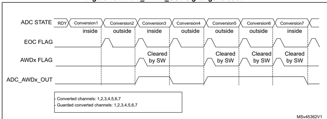
The diagram illustrates the timing relationship between the ADC state, End of Conversion (EOC) flags, Analog Watchdog (AWDx) flags, and the ADC_AWDx_OUT signal across seven conversions. The ADC STATE shows a sequence of 'RDY', 'Conversion1' (inside), 'Conversion2' (outside), 'Conversion3' (inside), 'Conversion4' (outside), 'Conversion5' (outside), 'Conversion6' (outside), and 'Conversion7' (inside). The EOC FLAG pulses at the end of each conversion. The AWDx FLAG is set when a conversion is 'outside' and is manually 'Cleared by SW' after each such conversion. The ADC_AWDx_OUT signal is shown toggling based on these 'outside' conversions, with edges occurring two clock cycles after the comparison. A legend indicates that channels 1, 2, 3, 4, 5, 6, and 7 are both 'Converted channels' and 'Guarded converted channels'.
MSv45362V1
Figure 102. ADC_AWDx_OUT signal generation (AWDx flag not cleared by software)
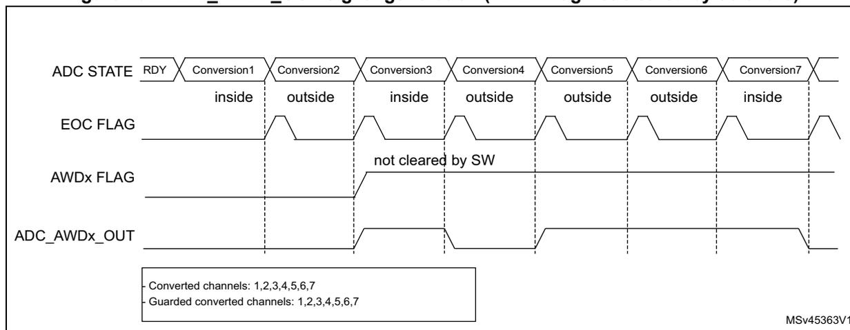
ADC STATE: RDY, Conversion1 (inside), Conversion2 (outside), Conversion3 (inside), Conversion4 (outside), Conversion5 (outside), Conversion6 (outside), Conversion7 (inside)
EOC FLAG: Pulses at the end of each conversion.
AWDx FLAG: Goes high at the end of Conversion 2 and remains high (not cleared by SW) until the end of Conversion 7.
ADC_AWDx_OUT: Goes high at the end of Conversion 2 and remains high until the end of Conversion 7.
Legend:
- Converted channels: 1,2,3,4,5,6,7
- Guarded converted channels: 1,2,3,4,5,6,7
MSV45363V1
Figure 103. ADC_AWDx_OUT signal generation (on a single channel)
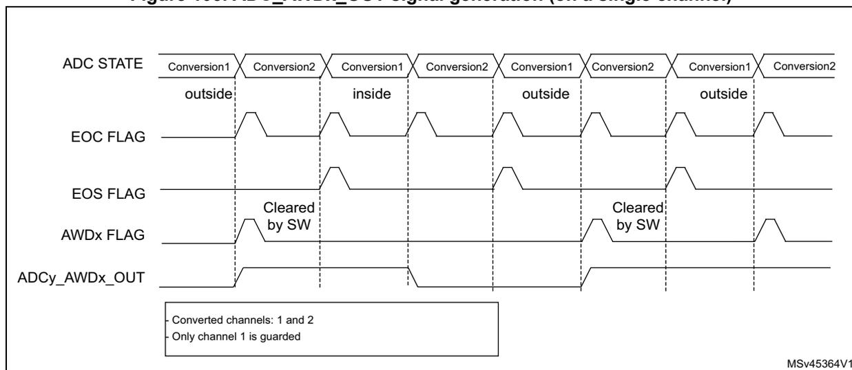
ADC STATE: Conversion1 (outside), Conversion2, Conversion1 (inside), Conversion2, Conversion1 (outside), Conversion2, Conversion1 (outside), Conversion2
EOC FLAG: Pulses at the end of each conversion.
EOS FLAG: Pulses at the end of each pair of conversions (Conversion 2).
AWDx FLAG: Goes high at the end of the first 'inside' conversion (Conversion 1) and is cleared by software. It goes high again at the end of the third 'inside' conversion (Conversion 1) and is cleared by software.
ADCy_AWDx_OUT: Goes high at the end of the first 'inside' conversion (Conversion 1) and remains high until the end of the third 'inside' conversion (Conversion 1).
Legend:
- Converted channels: 1 and 2
- Only channel 1 is guarded
MSV45364V1
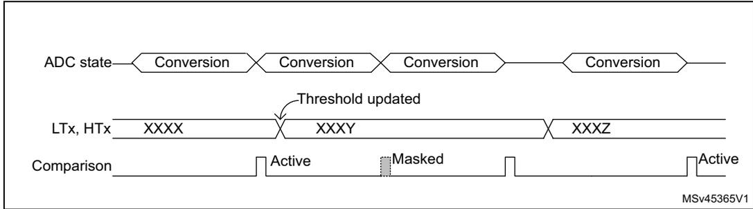
Analog watchdog threshold control
LTx[11:0] and HTx[11:0] can be changed during an analog-to-digital conversion (that is between the start of the conversion and the end of conversion of the ADC internal state). If HTx and LTx bits are programmed during the ADC guarded channel conversion, the watchdog function is masked for this conversion. This mask is cleared when starting a new conversion, and the resulting new AWD threshold is applied starting the next ADC conversion result. AWD comparison is performed at each end of conversion. If the current ADC data are out of the new threshold interval, this does not generate any interrupt or an ADC_AWDx_OUT signal. The Interrupt and the ADC_AWDx_OUT generation only occurs at the end of the ADC conversion that started after the threshold update. If ADC_AWDx_OUT is already asserted, programming the new threshold does not deassert the ADC_AWDx_OUT signal.
Figure 104. Analog watchdog threshold update
22.4.26 Oversampler
The oversampling unit performs data preprocessing to offload the CPU. It can handle multiple conversions and average them into a single data with increased data width, up to 16-bit.
It provides a result with the following form, where N and M can be adjusted:
It allows the following functions to be performed by hardware: averaging, data rate reduction, SNR improvement, basic filtering.
The oversampling ratio N is defined using the OVSR[2:0] bits in the ADC_CFGR2 register. It can range from 2x to 256x. The division coefficient M consists of a right bit shift up to 8 bits. It is configured through the OVSS[3:0] bits in the ADC_CFGR2 register.
The summation unit can yield a result up to 20 bits (256 x 12-bit), which is first shifted right. The lower bits of the result are then truncated, keeping only the 16 least significant bits rounded to the nearest value using the least significant bits left apart by the shifting, before being finally transferred into the ADC_DR data register.
Note: If the intermediate result after the shifting exceeds 16 bits, the upper bits of the result are simply truncated.
Figure 105. 20-bit to 16-bit result truncation
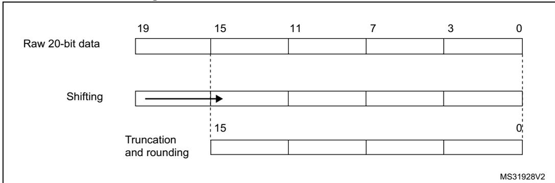
The Figure 106 gives a numerical example of the processing, from a raw 20-bit accumulated data to the final 16-bit result.
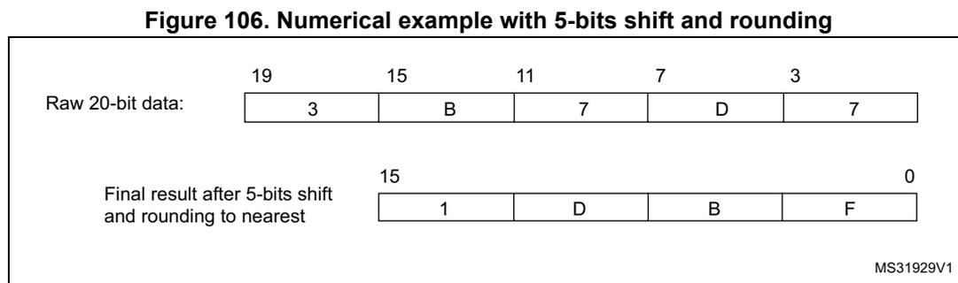
Figure 106. Numerical example with 5-bits shift and rounding
| Raw 20-bit data: | 19 | 15 | 11 | 7 | 3 | |||||
| 3 | B | 7 | D | 7 | ||||||
| Final result after 5-bits shift and rounding to nearest | 15 | 0 | ||||||||
| 1 | D | B | F | |||||||
MS31929V1
The Table 173 below gives the data format for the various N and M combination, for a raw conversion data equal to 0xFFF.
Table 173. Maximum output results vs N and M. Grayed values indicates truncation
| Oversampling ratio | Max Raw data | No-shift | 1-bit shift | 2-bit shift | 3-bit shift | 4-bit shift | 5-bit shift | 6-bit shift | 7-bit shift | 8-bit shift |
|---|---|---|---|---|---|---|---|---|---|---|
| OVSS = 0000 | OVSS = 0001 | OVSS = 0010 | OVSS = 0011 | OVSS = 0100 | OVSS = 0101 | OVSS = 0110 | OVSS = 0111 | OVSS = 1000 | ||
| 2x | 0x1FFE | 0x1FFE | 0x0FFF | 0x0800 | 0x0400 | 0x0200 | 0x0100 | 0x0080 | 0x0040 | 0x0020 |
| 4x | 0x3FFC | 0x3FFC | 0x1FFE | 0x0FFF | 0x0800 | 0x0400 | 0x0200 | 0x0100 | 0x0080 | 0x0040 |
| 8x | 0x7FF8 | 0x7FF8 | 0x3FFC | 0x1FFE | 0x0FFF | 0x0800 | 0x0400 | 0x0200 | 0x0100 | 0x0080 |
| 16x | 0xFFF0 | 0xFFF0 | 0x7FF8 | 0x3FFC | 0x1FFE | 0x0FFF | 0x0800 | 0x0400 | 0x0200 | 0x0100 |
| 32x | 0x1FFE0 | 0xFFE0 | 0xFFF0 | 0x7FF8 | 0x3FFC | 0x1FFE | 0x0FFF | 0x0800 | 0x0400 | 0x0200 |
| 64x | 0x3FFC0 | 0xFFC0 | 0xFFE0 | 0xFFF0 | 0x7FF8 | 0x3FFC | 0x1FFE | 0x0FFF | 0x0800 | 0x0400 |
| 128x | 0x7FF80 | 0xFF80 | 0xFFC0 | 0xFFE0 | 0xFFF0 | 0x7FF8 | 0x3FFC | 0x1FFE | 0x0FFF | 0x0800 |
| 256x | 0xFFF00 | 0xFF00 | 0xFF80 | 0xFFC0 | 0xFFE0 | 0xFFF0 | 0x7FF8 | 0x3FFC | 0x1FFE | 0x0FFF |
The conversion timings in oversampler mode do not change compared to standard conversion mode: the sample time is maintained equal during the whole oversampling sequence. New data are provided every N conversion, with an equivalent delay equal to \( N \times t_{CONV} = N \times (t_{SMPL} + t_{SAR}) \) . The flags features are raised as following:
- • the end of the sampling phase (EOSMP) is set after each sampling phase
- • the end of conversion (EOC) occurs once every N conversions, when the oversampled result is available
- • the end of sequence (EOCSEQ) occurs once the sequence of oversampled data is completed (i.e. after N x sequence length conversions total)
ADC operating modes supported when oversampling
In oversampling mode, most of the ADC operating modes are available:
- • Single or continuous mode conversions, forward or backward scanned sequences and up to 8 channels programmed sequence
- • ADC conversions start either by software or with triggers
- • ADC stop during a conversion (abort)
- • Data read via CPU or DMA with overrun detection
- • Low-power modes (WAIT, AUTOFF)
- • Programmable resolution: in this case, the reduced conversion values (as per RES[1:0] bits in ADC_CFGR1 register) are accumulated, truncated, rounded and shifted in the same way as 12-bit conversions are
Note: The alignment mode is not available when working with oversampled data. The ALIGN bit in ADC_CFGR1 is ignored and the data are always provided right-aligned.
Analog watchdog
The analog watchdog functionality is available, with the following differences:
- • the RES[1:0] bits are ignored, comparison is always done on using the full 12-bits values HTx[11:0] and LTx[11:0]
- • the comparison is performed on the most significant 12 bits of the 16 bits oversampled results ADC_DR[15:4]
Note: Care must be taken when using high shifting values. This reduces the comparison range. For instance, if the oversampled result is shifted by 4 bits thus yielding a 12-bit data right-aligned, the effective analog watchdog comparison can only be performed on 8 bits. The comparison is done between ADC_DR[11:4] and HTx[7:0] / LTx[7:0], and HTx[11:8] / LTx[11:8] must be kept reset.
Triggered mode
The averager can also be used for basic filtering purposes. Although not a very efficient filter (slow roll-off and limited stop band attenuation), it can be used as a notch filter to reject constant parasitic frequencies (typically coming from the mains or from a switched mode power supply). For this purpose, a specific discontinuous mode can be enabled with TOVS bit in ADC_CFGR2, to be able to have an oversampling frequency defined by a user and independent from the conversion time itself.
Figure 107 below shows how conversions are started in response to triggers in discontinuous mode.
If the TOVS bit is set, the content of the DISCEN bit is ignored and considered as 1.
Figure 107. Triggered oversampling mode (TOVS bit = 1)
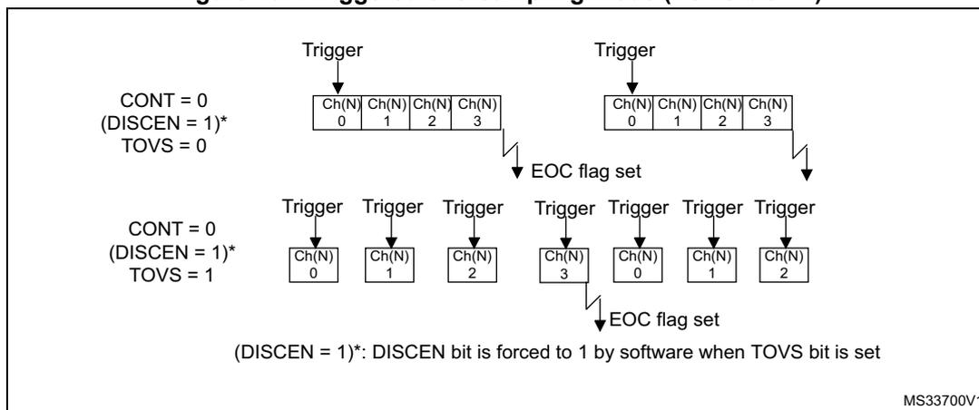
CONT = 0
(DISCEN = 1)*
TOVS = 0
Trigger
Ch(N) 0 Ch(N) 1 Ch(N) 2 Ch(N) 3
EOC flag set
CONT = 0
(DISCEN = 1)*
TOVS = 1
Trigger Trigger Trigger Trigger Trigger Trigger Trigger
Ch(N) 0 Ch(N) 1 Ch(N) 2 Ch(N) 3 Ch(N) 0 Ch(N) 1 Ch(N) 2
EOC flag set
(DISCEN = 1)*: DISCEN bit is forced to 1 by software when TOVS bit is set
MS33700V1
22.4.27 Temperature sensor and internal reference voltage
The temperature sensor can be used to measure the junction temperature ( \( T_j \) ) of the device. The temperature sensor is internally connected an ADC internal input channel which is used to convert the sensor's output voltage to a digital value. The sampling time for the temperature sensor analog pin must be greater than the minimum \( T_{S\_temp} \) value specified in the datasheet. When not in use, the sensor can be put in Power-down mode.
The internal voltage reference ( \( V_{REFINT} \) ) provides a stable (bandgap) voltage output for the ADC and the comparators.
Refer to Table ADC interconnection in Section 22.4.2: ADC pins and internal signals for details on the ADC internal input channel to which the above voltages are connected.
Figure 108 shows the block diagram of connections between the temperature sensor, the internal voltage reference and the ADC.
The VSENSESEL bit must be set to enable the conversion of \( V_{SENSE} \) while VREFEN bit must be set to enable the conversion of \( V_{REFINT} \) .
When the ADC operates in autonomous mode, these signals are controlled automatically to reduce power consumption (VSENSESEL and VREFEN must be set to measure the voltage in autonomous mode).
The temperature sensor output voltage linearly changes with the temperature. The offset of this line varies from chip to chip due to process variation (up to 45 °C from one chip to another).
The uncalibrated internal temperature sensor is more suited for applications that detect temperature variations instead of absolute temperatures. To improve the accuracy of the temperature sensor measurement, calibration values are stored in system memory for each device by STMicroelectronics during production.
During the manufacturing process, the calibration data of the temperature sensor and the internal voltage reference are stored in the system memory area. The user application can then read them and use them to improve the accuracy of the temperature sensor or the internal reference. Refer to the datasheet for additional information.
Main features
- Linearity: \( \pm 2\text{ }^{\circ}\text{C} \) max., precision depending on calibration
Figure 108. Temperature sensor and \( V_{\text{REFINT}} \) channel block diagram
![Figure 108. Temperature sensor and V_REFINT channel block diagram. The diagram shows two input channels connected to an ADC. The top channel is labeled V_IN[0] and is connected to an internal power block through a buffer. The buffer is controlled by the VREFEN control bit. The bottom channel is labeled V_IN[13] and is connected to a temperature sensor through a buffer. This buffer is controlled by the VSENSESEL control bit. Both channels output to a common 'Address/data bus' which provides 'converted data'.](/RM0521-STM32WBA2/5478c8d58d46b842394b57d0a238bc9e_img.jpg)
Reading the temperature
- 1. Select the input channel connected to \( V_{\text{SENSE}} \) (refer to Table ADC interconnection in Section 22.4.2: ADC pins and internal signals ).
- 2. Select an appropriate sampling time specified in the device datasheet ( \( T_{\text{S\_temp}} \) ).
- 3. Set the VSENSESEL bit in the ADC_CCR register to wake up the temperature sensor from power-down mode and wait for its stabilization time ( \( t_{\text{START}} \) ).
- 4. Start the ADC conversion by setting the ADSTART bit in the ADC_CR register (or by external trigger)
- 5. Read the resulting \( V_{\text{SENSE}} \) data in the ADC_DR register
- 6. Calculate the temperature using the following formula
Where:
- – TS_CAL2 is the temperature sensor calibration value acquired at TS_CAL2_TEMP.
- – TS_CAL1 is the temperature sensor calibration value acquired at TS_CAL1_TEMP.
- – TS_DATA is the actual temperature sensor output value converted by the ADC.
Refer to Section 22.3: ADC implementation for more information on TS_CAL1 and TS_CAL2 calibration points.
Note: The sensor has a startup time after waking up from power-down mode before it can output \( V_{\text{SENSE}} \) at the correct level. The ADC also has a startup time after power-on, so to minimize the delay, the ADEN and VSENSESEL bits must be set at the same time.
Calculating the actual \( V_{DDA} \) voltage using the internal reference voltage
The \( V_{DDA} \) power supply voltage applied to the microcontroller may be subject to variation or not precisely known. The embedded internal voltage reference (VREFINT) and its calibration data acquired by the ADC during the manufacturing process at \( V_{DDA} = 3.0\text{ V} \) can be used to evaluate the actual \( V_{DDA} \) voltage level.
The following formula gives the actual \( V_{DDA} \) voltage supplying the device:
Where:
- • VREFINT_CAL is the VREFINT calibration value
- • VREFINT_DATA is the actual VREFINT output value converted by ADC
Converting a supply-relative ADC measurement to an absolute voltage value
The ADC is designed to deliver a digital value corresponding to the ratio between the voltage reference \( V_{DDA} \) and the voltage applied on the converted channel. For most application use cases, it is necessary to convert this ratio into a voltage independent from \( V_{DDA} \) . For applications where \( V_{DDA} \) is known and ADC converted values are right-aligned, the following formula can be used to calculate this absolute value:
For applications where \( V_{DDA} \) value is not known, the internal voltage reference and \( V_{DDA} \) can be replaced by the expression provided in Section : Calculating the actual \( V_{DDA} \) voltage using the internal reference voltage , resulting in the following formula:
Where:
- • VREFINT_CAL is the VREFINT calibration value (refer to Section 22.3: ADC implementation for the value of VREFINT_CAL).
- • ADC_DATA x is the value measured by the ADC on channelx (right-aligned).
- • VREFINT_DATA is the actual VREFINT output value converted by the ADC.
- • FULL_SCALE is the maximum digital value of the ADC output. For example with 12-bit resolution, it is \( 2^{12} - 1 = 4095 \) or with 8-bit resolution, \( 2^8 - 1 = 255 \) .
Note: If ADC measurements are done using an output format other than 12 bit right-aligned, all the parameters must first be converted to a compatible format before the calculation is done.
22.5 ADC in low-power modes
Table 174. Effect of low-power modes on the ADC
| Mode | Description |
|---|---|
| Sleep | No effect, DMA requests are functional. ADC interrupts cause the device to exit Sleep mode. |
| Stop 0 and Stop 1 | The content of the ADC register is kept. ADC can be functional. DMA request are functional, and the interrupt cause the device to exit Stop mode. |
| Stop 2, Stop 3, Standby | The ADC peripheral is powered down and must be reinitialized after exiting Stop 2, Stop 3, and Standby modes. |
22.6 ADC interrupts
An interrupt can be generated by any of the following events:
- • End of calibration (EOCAL flag)
- • ADC power-up, when the ADC is ready (ADRDY flag)
- • End of any conversion (EOC flag)
- • End of a sequence of conversions (EOS flag)
- • When an analog watchdog detection occurs (AWD1, AWD2, AWD3 flags)
- • When the end of sampling phase occurs (EOSMP flag)
- • when a data overrun occurs (OVR flag)
- • LDO ready, when LDO output is stabilized (LDORDY flag)
Separate interrupt enable bits are available for flexibility.
Table 175. ADC wake-up and interrupt requests
| Interrupt vector | Interrupt event | Event flag | Enable Control bit | Interrupt clear method | Exit from Sleep mode | Exit from Stop mode (1) | Exit from Standby mode |
|---|---|---|---|---|---|---|---|
| ADC | LDO ready | LDORDY | LDORDYIE | Program LDORDY to 1 | Yes | Yes | No |
| End of calibration | EOCAL | EOCALIE | Program EOCAL to 1 | Yes | |||
| ADC ready | ADRDY | ADRDYIE | Program ADRDY to 1 | Yes | |||
| End of conversion | EOC | EOCIE | Program EOC to 1 OR read ADC_DR | Yes | |||
| End of sequence of conversions | EOS | EOSIE | Program EOS to 1 | Yes | |||
| Analog watchdog 1 status bit is set | AWD1 | AWD1IE | Program AWD1 to 1 | Yes | |||
| Analog watchdog 2 status bit is set | AWD2 | AWD2IE | Program AWD2 to 1 | Yes | |||
| Analog watchdog 3 status bit is set | AWD3 | AWD3IE | Program AWD2 to 1 | Yes | |||
| End of sampling phase | EOSMP | EOSMPIE | Program EOSMP to 1 | No | |||
| Overrun | OVR | OVRIE | Program OVR to 1 | Yes |
- 1. The ADC can wake up the device from Stop mode only if the peripheral instance supports the wake-up from Stop mode feature. Refer to Section 22.3: ADC implementation for the list of supported Stop modes.
22.7 ADC registers
Refer to Section 1.2 for a list of abbreviations used in register descriptions.
22.7.1 ADC interrupt and status register (ADC_ISR)
Address offset: 0x00
Reset value: 0x0000 0000
| 31 | 30 | 29 | 28 | 27 | 26 | 25 | 24 | 23 | 22 | 21 | 20 | 19 | 18 | 17 | 16 |
|---|---|---|---|---|---|---|---|---|---|---|---|---|---|---|---|
| Res. | Res. | Res. | Res. | Res. | Res. | Res. | Res. | Res. | Res. | Res. | Res. | Res. | Res. | Res. | Res. |
| 15 | 14 | 13 | 12 | 11 | 10 | 9 | 8 | 7 | 6 | 5 | 4 | 3 | 2 | 1 | 0 |
| Res. | Res. | Res. | LDO RDY | EOCAL | Res. | AWD3 | AWD2 | AWD1 | Res. | Res. | OVR | EOS | EOC | EOSMP | ADRDY |
| rc_w1 | rc_w1 | rc_w1 | rc_w1 | rc_w1 | rc_w1 | rc_w1 | rc_w1 | rc_w1 | rc_w1 |
Bits 31:13 Reserved, must be kept at reset value.
Bit 12 LDORDY : LDO ready
This bit is set by hardware. It indicates that the ADC internal LDO output is ready.
It is cleared by software by writing 1 to it.
0: ADC voltage regulator disabled
1: ADC voltage regulator enabled and stabilized
Bit 11 EOCAL : End of calibration flag
This bit is set by hardware when calibration is complete. It is cleared by software writing 1 to it.
0: Calibration is not complete
1: Calibration is complete
Bit 10 Reserved, must be kept at reset value.
Bit 9 AWD3 : Analog watchdog 3 flag
This bit is set by hardware when the converted voltage crosses the values programmed in ADC_AWD3TR and ADC_AWD3TR registers. It is cleared by software by writing 1 to it.
0: No analog watchdog event occurred (or the flag event was already acknowledged and cleared by software)
1: Analog watchdog event occurred
Bit 8 AWD2 : Analog watchdog 2 flag
This bit is set by hardware when the converted voltage crosses the values programmed in ADC_AWD2TR and ADC_AWD2TR registers. It is cleared by software writing 1 to it.
0: No analog watchdog event occurred (or the flag event was already acknowledged and cleared by software)
1: Analog watchdog event occurred
Bit 7 AWD1 : Analog watchdog 1 flag
This bit is set by hardware when the converted voltage crosses the values programmed in ADC_TR1 and ADC_HR1 registers. It is cleared by software by writing 1 to it.
0: No analog watchdog event occurred (or the flag event was already acknowledged and cleared by software)
1: Analog watchdog event occurred
Bits 6:5 Reserved, must be kept at reset value.
Bit 4 OVR : ADC overrun
This bit is set by hardware when an overrun occurs, meaning that a new conversion has complete while the EOC flag was already set. It is cleared by software writing 1 to it.
0: No overrun occurred (or the flag event was already acknowledged and cleared by software)
1: Overrun has occurred
Bit 3 EOS : End of sequence flag
This bit is set by hardware at the end of the conversion of a sequence of channels selected by the CHSEL bits. It is cleared by software writing 1 to it.
0: Conversion sequence not complete (or the flag event was already acknowledged and cleared by software)
1: Conversion sequence complete
Bit 2 EOC : End of conversion flag
This bit is set by hardware at the end of each conversion of a channel when a new data result is available in the ADC_DR register. It is cleared by software writing 1 to it or by reading the ADC_DR register.
0: Channel conversion not complete (or the flag event was already acknowledged and cleared by software)
1: Channel conversion complete
Bit 1 EOSMP : End of sampling flag
This bit is set by hardware during the conversion, at the end of the sampling phase. It is cleared by software by writing 1 to it.
0: Not at the end of the sampling phase (or the flag event was already acknowledged and cleared by software)
1: End of sampling phase reached
Bit 0 ADDRDY : ADC ready
This bit is set by hardware after the ADC has been enabled (ADEN = 1) and when the ADC reaches a state where it is ready to accept conversion requests.
It is cleared by software writing 1 to it.
0: ADC not yet ready to start conversion (or the flag event was already acknowledged and cleared by software)
1: ADC is ready to start conversion
22.7.2 ADC interrupt enable register (ADC_IER)
Address offset: 0x04
Reset value: 0x0000 0000
| 31 | 30 | 29 | 28 | 27 | 26 | 25 | 24 | 23 | 22 | 21 | 20 | 19 | 18 | 17 | 16 |
|---|---|---|---|---|---|---|---|---|---|---|---|---|---|---|---|
| Res. | Res. | Res. | Res. | Res. | Res. | Res. | Res. | Res. | Res. | Res. | Res. | Res. | Res. | Res. | Res. |
| 15 | 14 | 13 | 12 | 11 | 10 | 9 | 8 | 7 | 6 | 5 | 4 | 3 | 2 | 1 | 0 |
| Res. | Res. | Res. | LDORD YIE | EOCAL IE | Res. | AWD3 IE | AWD2 IE | AWD1 IE | Res. | Res. | OVR IE | EOS IE | EOC IE | EOSMP IE | ADDR DY IE |
| rw | rw | rw | rw | rw | rw | rw | rw | rw | rw |
Bits 31:13 Reserved, must be kept at reset value.
Bit 12 LDORDYIE : LDO ready interrupt enable
This bit is set and cleared by software. It is used to enable/disable the LDORDY interrupt.
0: LDO ready interrupt disabled
1: LDO ready interrupt enabled. An interrupt is generated when the LDO output is ready.
Note: The software is allowed to write this bit only when ADSTART bit is cleared to 0 by writing ADSTP to 1 (this ensure that no conversion is ongoing).
Bit 11 EOCALIE : End of calibration interrupt enable
This bit is set and cleared by software to enable/disable the end of calibration interrupt.
0: End of calibration interrupt disabled
1: End of calibration interrupt enabled
Note: The software is allowed to write this bit only when ADSTART bit is cleared to 0 by writing ADSTP to 1 (this ensures that no conversion is ongoing).
Bit 10 Reserved, must be kept at reset value.
Bit 9 AWD3IE : Analog watchdog 3 interrupt enable
This bit is set and cleared by software to enable/disable the analog watchdog interrupt.
0: Analog watchdog interrupt disabled
1: Analog watchdog interrupt enabled
Note: The Software is allowed to write this bit only when ADSTART bit is cleared to 0 by writing ADSTP to 1 (this ensures that no conversion is ongoing).
Bit 8 AWD2IE : Analog watchdog 2 interrupt enable
This bit is set and cleared by software to enable/disable the analog watchdog interrupt.
0: Analog watchdog interrupt disabled
1: Analog watchdog interrupt enabled
Note: The Software is allowed to write this bit only when ADSTART bit is cleared to 0 by writing ADSTP to 1 (this ensures that no conversion is ongoing).
Bit 7 AWD1IE : Analog watchdog 1 interrupt enable
This bit is set and cleared by software to enable/disable the analog watchdog interrupt.
0: Analog watchdog interrupt disabled
1: Analog watchdog interrupt enabled
Note: The Software is allowed to write this bit only when ADSTART bit is cleared to 0 by writing ADSTP to 1 (this ensures that no conversion is ongoing).
Bits 6:5 Reserved, must be kept at reset value.
Bit 4 OVRIE : Overrun interrupt enable
This bit is set and cleared by software to enable/disable the overrun interrupt.
0: Overrun interrupt disabled
1: Overrun interrupt enabled. An interrupt is generated when the OVR bit is set.
Note: The software is allowed to write this bit only when ADSTART bit is cleared to 0 by writing ADSTP to 1 (this ensures that no conversion is ongoing).
Bit 3 EOSIE : End of conversion sequence interrupt enable
This bit is set and cleared by software to enable/disable the end of sequence of conversions interrupt.
0: EOS interrupt disabled
1: EOS interrupt enabled. An interrupt is generated when the EOS bit is set.
Note: The software is allowed to write this bit only when ADSTART bit is cleared to 0 by writing ADSTP to 1 (this ensures that no conversion is ongoing).
Bit 2 EOCIE: End of conversion interrupt enableThis bit is set and cleared by software to enable/disable the end of conversion interrupt.
0: EOC interrupt disabled
1: EOC interrupt enabled. An interrupt is generated when the EOC bit is set.
Note: The software is allowed to write this bit only when ADSTART bit is cleared to 0 by writing ADSTP to 1 (this ensures that no conversion is ongoing).
Bit 1 EOSMPIE: End of sampling flag interrupt enableThis bit is set and cleared by software to enable/disable the end of the sampling phase interrupt.
0: EOSMP interrupt disabled.
1: EOSMP interrupt enabled. An interrupt is generated when the EOSMP bit is set.
Note: The software is allowed to write this bit only when ADSTART bit is cleared to 0 by writing ADSTP to 1 (this ensures that no conversion is ongoing).
Bit 0 ADRDYIE: ADC ready interrupt enableThis bit is set and cleared by software to enable/disable the ADC Ready interrupt.
0: ADRDY interrupt disabled.
1: ADRDY interrupt enabled. An interrupt is generated when the ADRDY bit is set.
Note: The software is allowed to write this bit only when ADSTART bit is cleared to 0 by writing ADSTP to 1 (this ensures that no conversion is ongoing).
22.7.3 ADC control register (ADC_CR)
Address offset: 0x08
Reset value: 0x0000 0000
| 31 | 30 | 29 | 28 | 27 | 26 | 25 | 24 | 23 | 22 | 21 | 20 | 19 | 18 | 17 | 16 |
|---|---|---|---|---|---|---|---|---|---|---|---|---|---|---|---|
| ADCAL | Res. | Res. | ADVREGEN | Res. | Res. | Res. | Res. | Res. | Res. | Res. | Res. | Res. | Res. | Res. | Res. |
| rs | rw | ||||||||||||||
| 15 | 14 | 13 | 12 | 11 | 10 | 9 | 8 | 7 | 6 | 5 | 4 | 3 | 2 | 1 | 0 |
| Res. | Res. | Res. | Res. | Res. | Res. | Res. | Res. | Res. | Res. | Res. | ADSTP | Res. | ADSTART | ADDIS | ADEN |
| rs | rs | rs | rs |
Bit 31 ADCAL: ADC calibration
This bit is set by software to start the calibration of the ADC.
It is cleared by hardware after calibration is complete.
0: Calibration complete
1: Write 1 to calibrate the ADC. Read at 1 means that a calibration is in progress.
Note: The software is allowed to set ADCAL only when the ADC is disabled (ADCAL = 0, ADSTART = 0, ADSTP = 0, ADDIS = 0, AUTOFF = 0, and ADEN = 0).
The software is allowed to update the calibration factor by writing ADC_CALFACT only when ADEN is set to 1 and ADSTART is cleared to 0 by writing ADSTP to 1 (ADC enabled and no conversion is ongoing).
Bits 30:29 Reserved, must be kept at reset value.
Bit 28 ADVREGEN: ADC voltage regulator enable
This bit is set by software, to enable the ADC internal voltage regulator. The voltage regulator output is available after
\(
t_{\text{ADCVREG\_SETUP}}
\)
.
It is cleared by software to disable the voltage regulator. It can be cleared only if ADEN is set to 0.
0: ADC voltage regulator disabled
1: ADC voltage regulator enabled
Note: The software is allowed to program this bit field only when the ADC is disabled (ADCAL = 0, ADSTART = 0, ADSTP = 0, ADDIS = 0 and ADEN = 0).
Bits 27:5 Reserved, must be kept at reset value.
Bit 4 ADSTP: ADC stop conversion command
This bit is set by software to stop and discard an ongoing conversion (ADSTP Command).
It is cleared by hardware when the conversion is effectively discarded and the ADC is ready to accept a new start conversion command.
0: No ADC stop conversion command ongoing
1: Write 1 to stop the ADC. Read 1 means that an ADSTP command is in progress.
Note: To clear the A/D converter state, ADSTP must be set to 1 even if ADSTART is cleared to 0 after the software trigger A/D conversion. It is recommended to set ADSTP to 1 whenever the configuration needs to be modified.
Bit 3 Reserved, must be kept at reset value.
Bit 2 ADSTART: ADC start conversion commandThis bit is set by software to start ADC conversion. Depending on the EXTEN [1:0] configuration bits, a conversion either starts immediately (software trigger configuration) or once a hardware trigger event occurs (hardware trigger configuration).
It is cleared by hardware:
- – In single conversion mode (CONT = 0, DISCEN = 0), when software trigger is selected (EXTEN = 00): at the assertion of the end of Conversion Sequence (EOS) flag.
- – In discontinuous conversion mode (CONT=0, DISCEN = 1), when the software trigger is selected (EXTEN = 00): at the assertion of the end of Conversion (EOC) flag.
- – In all other cases: after the execution of the ADSTP command, at the same time as the ADSTP bit is cleared by hardware.
0: No ADC conversion is ongoing.
1: Write 1 to start the ADC. Read 1 means that the ADC is operating and may be converting.
Note: The software is allowed to set ADSTART only when ADEN = 1 and ADDIS = 0 (ADC is enabled and there is no pending request to disable the ADC).
Bit 1 ADDIS: ADC disable commandThis bit is set by software to disable the ADC (ADDIS command) and put it into power-down state (OFF state).
It is cleared by hardware once the ADC is effectively disabled (ADEN is also cleared by hardware at this time).
0: No ADDIS command ongoing
1: Write 1 to disable the ADC. Read 1 means that an ADDIS command is in progress.
Note: Setting ADDIS to 1 is only effective when ADEN = 1 and ADSTART = 0 (which ensures that no conversion is ongoing)
Bit 0 ADEN: ADC enable commandThis bit is set by software to enable the ADC. The ADC is effectively ready to operate once the ADRDY flag has been set.
It is cleared by hardware when the ADC is disabled, after the execution of the ADDIS command.
0: ADC is disabled (OFF state)
1: Write 1 to enable the ADC.
Note: The software is allowed to set ADEN only when all bits of ADC_CR registers are 0 (ADCAL = 0, ADSTP = 0, ADSTART = 0, ADDIS = 0 and ADEN = 0)
22.7.4 ADC configuration register 1 (ADC_CFGR1)
Address offset: 0x0C
Reset value: 0x0000 0000
| 31 | 30 | 29 | 28 | 27 | 26 | 25 | 24 | 23 | 22 | 21 | 20 | 19 | 18 | 17 | 16 |
|---|---|---|---|---|---|---|---|---|---|---|---|---|---|---|---|
| Res. | AWD1CH[4:0] | Res. | Res. | AWD1EN | AWD1SGL | CHSEL RMOD | Res. | Res. | Res. | Res. | DISCEN | ||||
| rw | rw | rw | rw | rw | rw | rw | rw | rw | |||||||
| 15 | 14 | 13 | 12 | 11 | 10 | 9 | 8 | 7 | 6 | 5 | 4 | 3 | 2 | 1 | 0 |
|---|---|---|---|---|---|---|---|---|---|---|---|---|---|---|---|
| Res. | WAIT | CONT | OVRMOD | EXTEN[1:0] | Res. | EXTSEL[2:0] | ALIGN | SCAN DIR | RES[1:0] | DMAC FG | DMAEN | ||||
| rw | rw | rw | rw | rw | rw | rw | rw | rw | rw | rw | rw | rw | rw | ||
Bit 31 Reserved, must be kept at reset value.
Bits 30:26 AWD1CH[4:0] : Analog watchdog channel selection
These bits are set and cleared by software. They select the input channel to be guarded by the analog watchdog.
00000: ADC analog input Channel 0 monitored by AWD
00001: ADC analog input Channel 1 monitored by AWD
.....
01101: ADC analog input Channel 13 monitored by AWD
Others: Reserved
Note: The channel selected by the AWDCH[4:0] bits must be also set into the CHSELR register. The software is allowed to write this bit only when ADSTART bit is cleared to 0 by writing ADSTP to 1 (this ensures that no conversion is ongoing).
Bits 25:24 Reserved, must be kept at reset value.
Bit 23 AWD1EN : Analog watchdog enable
This bit is set and cleared by software.
0: Analog watchdog 1 disabled
1: Analog watchdog 1 enabled
Note: The software is allowed to write this bit only when ADSTART bit is cleared to 0 by writing ADSTP to 1 (this ensures that no conversion is ongoing).
Bit 22 AWD1SGL : Enable the watchdog on a single channel or on all channels
This bit is set and cleared by software to enable the analog watchdog on the channel identified by the AWDCH[4:0] bits or on all the channels
0: Analog watchdog 1 enabled on all channels
1: Analog watchdog 1 enabled on a single channel
Note: The software is allowed to write this bit only when ADSTART bit is cleared to 0 by writing ADSTP to 1 (this ensures that no conversion is ongoing).
Bit 21 CHSELRMOD : Mode selection of the ADC_CHSELR register
This bit is set and cleared by software to control the ADC_CHSELR feature:
0: Each bit of the ADC_CHSELR register enables an input
1: ADC_CHSELR register is able to sequence up to 8 channels
Note: The software is allowed to write this bit only when ADSTART bit is cleared to 0 by writing ADSTP to 1 (this ensures that no conversion is ongoing).
Bits 20:17 Reserved, must be kept at reset value.
Bit 16 DISCEN : Discontinuous modeThis bit is set and cleared by software to enable/disable discontinuous mode.
0: Discontinuous mode disabled
1: Discontinuous mode enabled
Note: It is not possible to have both discontinuous mode and continuous mode enabled: it is forbidden to set both bits DISCEN = 1 and CONT = 1.
The software is allowed to write this bit only when ADSTART bit is cleared to 0 by writing ADSTP to 1 (this ensures that no conversion is ongoing).
Bit 15 Reserved, must be kept at reset value.
Bit 14 WAIT : Wait conversion modeThis bit is set and cleared by software to enable/disable wait conversion mode.
0: Wait conversion mode off
1: Wait conversion mode on
Note: The software is allowed to write this bit only when ADSTART bit is cleared to 0 by writing ADSTP to 1 (this ensures that no conversion is ongoing).
Bit 13 CONT : Single / continuous conversion modeThis bit is set and cleared by software. If it is set, conversion takes place continuously until it is cleared.
0: Single conversion mode
1: Continuous conversion mode
Note: It is not possible to have both discontinuous mode and continuous mode enabled: it is forbidden to set both bits DISCEN = 1 and CONT = 1.
The software is allowed to write this bit only when ADSTART bit is cleared to 0 by writing ADSTP to 1 (this ensures that no conversion is ongoing).
Bit 12 OVRMOD : Overrun management modeThis bit is set and cleared by software and configure the way data overruns are managed.
0: ADC_DR register is preserved with the old data when an overrun is detected.
1: ADC_DR register is overwritten with the last conversion result when an overrun is detected.
Note: The software is allowed to write this bit only when ADSTART bit is cleared to 0 by writing ADSTP to 1 (this ensures that no conversion is ongoing).
Bits 11:10 EXTEN[1:0] : External trigger enable and polarity selectionThese bits are set and cleared by software to select the external trigger polarity and enable the trigger.
00: Hardware trigger detection disabled (conversions can be started by software)
01: Hardware trigger detection on the rising edge
10: Hardware trigger detection on the falling edge
11: Hardware trigger detection on both the rising and falling edges
Note: The software is allowed to write this bit only when ADSTART bit is cleared to 0 by writing ADSTP to 1 (this ensures that no conversion is ongoing).
Bit 9 Reserved, must be kept at reset value.
Bits 8:6 EXTSEL[2:0] : External trigger selectionThese bits select the external event used to trigger the start of conversion (refer to table ADC interconnection in Section 22.4.2: ADC pins and internal signals for details):
- 000: adc_trg0
- 001: adc_trg1
- 010: adc_trg2
- 011: adc_trg3
- 100: adc_trg4
- 101: adc_trg5
- 110: adc_trg6
- 111: adc_trg7
Note: The software is allowed to write this bit only when ADSTART bit is cleared to 0 by writing ADSTP to 1 (this ensures that no conversion is ongoing).
Bit 5 ALIGN : Data alignmentThis bit is set and cleared by software to select right or left alignment. Refer to Figure 93: Data alignment and resolution (oversampling disabled: OVSE = 0)
- 0: Right alignment
- 1: Left alignment
Note: The software is allowed to write this bit only when ADSTART bit is cleared to 0 by writing ADSTP to 1 (this ensures that no conversion is ongoing).
Bit 4 SCANDIR : Scan sequence directionThis bit is set and cleared by software to select the direction in which the channels is scanned in the sequence. It is effective only if CHSELRMOD bit is cleared to 0.
- 0: Upward scan (from CHSEL0 to CHSEL13)
- 1: Backward scan (from CHSEL13 to CHSEL0)
Note: The software is allowed to write this bit only when ADSTART bit is cleared to 0 by writing ADSTP to 1 (this ensures that no conversion is ongoing).
Bits 3:2 RES[1:0] : Data resolutionThese bits are written by software to select the resolution of the conversion.
- 00: 12 bits
- 01: 10 bits
- 10: 8 bits
- 11: 6 bits
Note: The software is allowed to write these bits only when ADSTART bit is cleared to 0 by writing ADSTP to 1 (this ensures that no conversion is ongoing).
Bit 1 DMACFG : Direct memory access configuration
This bit is set and cleared by software to select between two DMA modes of operation and is effective only when DMAEN = 1.
0: DMA one-shot mode selected
1: DMA circular mode selected
For more details, refer to Managing converted data using the DMA .
Note: The software is allowed to write this bit only when ADSTART bit is cleared to 0 by writing ADSTP to 1 (this ensures that no conversion is ongoing).
Bit 0 DMAEN : Direct memory access enable
This bit is set and cleared by software to enable the generation of DMA requests. This allows the automatic management of the converted data by the DMA controller. For more details, refer to Managing converted data using the DMA .
0: DMA disabled
1: DMA enabled
Note: The software is allowed to write this bit only when ADSTART bit is cleared to 0 by writing ADSTP to 1 (this ensures that no conversion is ongoing).
22.7.5 ADC configuration register 2 (ADC_CFGR2)
Address offset: 0x10
Reset value: 0x0000 0000
| 31 | 30 | 29 | 28 | 27 | 26 | 25 | 24 | 23 | 22 | 21 | 20 | 19 | 18 | 17 | 16 |
|---|---|---|---|---|---|---|---|---|---|---|---|---|---|---|---|
| Res. | Res. | LFTRIG | Res. | Res. | Res. | Res. | Res. | Res. | Res. | Res. | Res. | Res. | Res. | Res. | Res. |
| rw | |||||||||||||||
| 15 | 14 | 13 | 12 | 11 | 10 | 9 | 8 | 7 | 6 | 5 | 4 | 3 | 2 | 1 | 0 |
| Res. | Res. | Res. | Res. | Res. | Res. | TOVS | OVSS[3:0] | OVSR[2:0] | Res. | OVSE | |||||
| rw | rw | rw | rw | rw | rw | rw | rw | rw | |||||||
Bits 31:30 Reserved, must be kept at reset value.
Bit 29 LFTRIG : Low-frequency trigger mode enable
This bit must be set by software.
0: Reserved
1: Low-frequency trigger mode enabled.
Note: The software is allowed to write this bit only when ADSTART bit is cleared to 0 by writing ADSTP to 1 (this ensures that no conversion is ongoing).
Bits 28:10 Reserved, must be kept at reset value.
Bit 9 TOVS : Triggered Oversampling
This bit is set and cleared by software.
0: All oversampled conversions for a channel are done consecutively after a trigger
1: Each oversampled conversion for a channel needs a trigger
Note: The software is allowed to write this bit only when ADSTART is cleared to 0 by writing ADSTP to 1 (which ensures that no conversion is ongoing).
Bits 8:5 OVSS[3:0] : Oversampling shift
This bit is set and cleared by software.
- 0000: No shift
- 0001: Shift 1-bit
- 0010: Shift 2-bits
- 0011: Shift 3-bits
- 0100: Shift 4-bits
- 0101: Shift 5-bits
- 0110: Shift 6-bits
- 0111: Shift 7-bits
- 1000: Shift 8-bits
- Others: Reserved
Note: The software is allowed to write this bit only when ADSTART is cleared to 0 by writing ADSTP to 1 (which ensures that no conversion is ongoing).
Bits 4:2 OVSR[2:0] : Oversampling ratio
This bit field defines the number of oversampling ratio.
- 000: 2x
- 001: 4x
- 010: 8x
- 011: 16x
- 100: 32x
- 101: 64x
- 110: 128x
- 111: 256x
Note: The software is allowed to write this bit only when ADSTART is cleared to 0 by writing ADSTP to 1 (which ensures that no conversion is ongoing).
Bit 1 Reserved, must be kept at reset value.
Bit 0 OVSE : Oversampler Enable
This bit is set and cleared by software.
- 0: Oversampler disabled
- 1: Oversampler enabled
Note: Software is allowed to write this bit only when ADSTART is cleared to 0 by writing ADSTP to 1 (which ensures that no conversion is ongoing).
22.7.6 ADC sampling time register (ADC_SMPR)
Address offset: 0x14
Reset value: 0x0000 0000
| 31 | 30 | 29 | 28 | 27 | 26 | 25 | 24 | 23 | 22 | 21 | 20 | 19 | 18 | 17 | 16 |
|---|---|---|---|---|---|---|---|---|---|---|---|---|---|---|---|
| Res. | Res. | Res. | Res. | Res. | Res. | Res. | Res. | Res. | Res. | SMPSE L13 | SMPSE L12 | SMPSE L11 | SMPSE L10 | SMPSE L9 | SMPSE L8 |
| rw | rw | rw | rw | rw | rw | ||||||||||
| 15 | 14 | 13 | 12 | 11 | 10 | 9 | 8 | 7 | 6 | 5 | 4 | 3 | 2 | 1 | 0 |
| SMPSE L7 | SMPSE L6 | SMPSE L5 | SMPSE L4 | SMPSE L3 | SMPSE L2 | SMPSE L1 | SMPSE L0 | Res. | SMP2[2:0] | Res. | SMP1[2:0] | ||||
| rw | rw | rw | rw | rw | rw | rw | rw | rw | rw | rw | rw | rw | rw | ||
Bits 31:22 Reserved, must be kept at reset value.
Bits 21:8 SMPSELx : Channel-x sampling time selection (x = 13 to 0)
These bits are written by software to define which sampling time is used.
0: Sampling time of CHANNELx use the setting of SMP1[2:0] register.
1: Sampling time of CHANNELx use the setting of SMP2[2:0] register.
Note: The software is allowed to write this bit only when ADSTART is cleared to 0 by writing ADSTP to 1 (which ensures that no conversion is ongoing).
Bit 7 Reserved, must be kept at reset value.
Bits 6:4 SMP2[2:0] : Sampling time selection 2
These bits are written by software to select the sampling time that applies to all channels.
000: 1.5 ADC clock cycles
001: 3.5 ADC clock cycles
010: 7.5 ADC clock cycles
011: 12.5 ADC clock cycles
100: 19.5 ADC clock cycles
101: 39.5 ADC clock cycles
110: 79.5 ADC clock cycles
111: 814.5 ADC clock cycles
Note: The software is allowed to write this bit only when ADSTART is cleared to 0 by writing ADSTP to 1 (which ensures that no conversion is ongoing).
Bit 3 Reserved, must be kept at reset value.
Bits 2:0 SMP1[2:0] : Sampling time selection 1
These bits are written by software to select the sampling time that applies to all channels.
000: 1.5 ADC clock cycles
001: 3.5 ADC clock cycles
010: 7.5 ADC clock cycles
011: 12.5 ADC clock cycles
100: 19.5 ADC clock cycles
101: 39.5 ADC clock cycles
110: 79.5 ADC clock cycles
111: 814.5 ADC clock cycles
Note: The software is allowed to write this bit only when ADSTART is cleared to 0 by writing ADSTP to 1 (which ensures that no conversion is ongoing).
22.7.7 ADC watchdog threshold register (ADC_AWD1TR)
Address offset: 0x20
Reset value: 0x0FFF 0000
| 31 | 30 | 29 | 28 | 27 | 26 | 25 | 24 | 23 | 22 | 21 | 20 | 19 | 18 | 17 | 16 |
|---|---|---|---|---|---|---|---|---|---|---|---|---|---|---|---|
| Res. | Res. | Res. | Res. | HT1[11:0] | |||||||||||
| rw | rw | rw | rw | rw | rw | rw | rw | rw | rw | rw | rw | ||||
| 15 | 14 | 13 | 12 | 11 | 10 | 9 | 8 | 7 | 6 | 5 | 4 | 3 | 2 | 1 | 0 |
| Res. | Res. | Res. | Res. | LT1[11:0] | |||||||||||
| rw | rw | rw | rw | rw | rw | rw | rw | rw | rw | rw | rw | ||||
Bits 31:28 Reserved, must be kept at reset value.
Bits 27:16 HT1[11:0] : Analog watchdog 1 higher threshold
These bits are written by software to define the higher threshold for the analog watchdog.
Refer to Section 22.4.25: Analog window watchdog .
Bits 15:12 Reserved, must be kept at reset value.
Bits 11:0 LT1[11:0] : Analog watchdog 1 lower threshold
These bits are written by software to define the lower threshold for the analog watchdog.
Refer to Section 22.4.25: Analog window watchdog .
22.7.8 ADC watchdog threshold register (ADC_AWD2TR)
Address offset: 0x24
Reset value: 0x0FFF 0000
| 31 | 30 | 29 | 28 | 27 | 26 | 25 | 24 | 23 | 22 | 21 | 20 | 19 | 18 | 17 | 16 |
|---|---|---|---|---|---|---|---|---|---|---|---|---|---|---|---|
| Res. | Res. | Res. | Res. | HT2[11:0] | |||||||||||
| rw | rw | rw | rw | rw | rw | rw | rw | rw | rw | rw | rw | ||||
| 15 | 14 | 13 | 12 | 11 | 10 | 9 | 8 | 7 | 6 | 5 | 4 | 3 | 2 | 1 | 0 |
| Res. | Res. | Res. | Res. | LT2[11:0] | |||||||||||
| rw | rw | rw | rw | rw | rw | rw | rw | rw | rw | rw | rw | ||||
Bits 31:28 Reserved, must be kept at reset value.
Bits 27:16 HT2[11:0] : Analog watchdog 2 higher threshold
These bits are written by software to define the higher threshold for the analog watchdog.
Refer to Section 22.4.25: Analog window watchdog .
Bits 15:12 Reserved, must be kept at reset value.
Bits 11:0 LT2[11:0] : Analog watchdog 2 lower threshold
These bits are written by software to define the lower threshold for the analog watchdog.
Refer to Section 22.4.25: Analog window watchdog .
22.7.9 ADC channel selection register [alternate] (ADC_CHSELR)
Address offset: 0x28
Reset value: 0x0000 0000
The same register can be used in two different modes:
- – Each ADC_CHSELR bit enables an input (CHSELRMOD = 0 in ADC_CFGR1). Refer to the current section.
- – ADC_CHSELR is able to sequence up to 8 channels (CHSELRMOD = 1 in ADC_CFGR1). Refer to next section.
CHSELRMOD = 0 in ADC_CFGR1
| 31 | 30 | 29 | 28 | 27 | 26 | 25 | 24 | 23 | 22 | 21 | 20 | 19 | 18 | 17 | 16 |
|---|---|---|---|---|---|---|---|---|---|---|---|---|---|---|---|
| Res. | Res. | Res. | Res. | Res. | Res. | Res. | Res. | Res. | Res. | Res. | Res. | Res. | Res. | Res. | Res. |
| 15 | 14 | 13 | 12 | 11 | 10 | 9 | 8 | 7 | 6 | 5 | 4 | 3 | 2 | 1 | 0 |
| Res. | Res. | CHSEL 13 | CHSEL 12 | CHSEL 11 | CHSEL 10 | CHSEL 9 | CHSEL 8 | CHSEL 7 | CHSEL 6 | CHSEL 5 | CHSEL 4 | CHSEL 3 | CHSEL 2 | CHSEL 1 | CHSEL 0 |
| rw | rw | rw | rw | rw | rw | rw | rw | rw | rw | rw | rw | rw | rw | ||
Bits 31:14 Reserved, must be kept at reset value.
Bits 13:0 CHSELx : Channel x selection (x = 13 to 0)
These bits are written by software and define which channels are part of the sequence of channels to be converted.
0: Input Channel-x is not selected for conversion
1: Input Channel-x is selected for conversion
Note: The software is allowed to write this bit only when ADSTART is cleared to 0 by writing ADSTP to 1 (which ensures that no conversion is ongoing).
22.7.10 ADC channel selection register [alternate] (ADC_CHSELR)
Address offset: 0x28
Reset value: 0x0000 0000
The same register can be used in two different modes:
- – Each ADC_CHSELR bit enables an input (CHSELRMOD = 0 in ADC_CFGR1). Refer to the current previous section.
- – ADC_CHSELR is able to sequence up to 8 channels (CHSELRMOD = 1 in ADC_CFGR1). Refer to this section.
CHSELRMOD = 1 in ADC_CFGR1
| 31 | 30 | 29 | 28 | 27 | 26 | 25 | 24 | 23 | 22 | 21 | 20 | 19 | 18 | 17 | 16 |
|---|---|---|---|---|---|---|---|---|---|---|---|---|---|---|---|
| SQ8[3:0] | SQ7[3:0] | SQ6[3:0] | SQ5[3:0] | ||||||||||||
| rw | rw | rw | rw | rw | rw | rw | rw | rw | rw | rw | rw | rw | rw | rw | rw |
| 15 | 14 | 13 | 12 | 11 | 10 | 9 | 8 | 7 | 6 | 5 | 4 | 3 | 2 | 1 | 0 |
| SQ4[3:0] | SQ3[3:0] | SQ2[3:0] | SQ1[3:0] | ||||||||||||
| rw | rw | rw | rw | rw | rw | rw | rw | rw | rw | rw | rw | rw | rw | rw | rw |
These bits are programmed by software with the channel number assigned to the 8th conversion of the sequence. 0b1111 indicates the end of the sequence.
When 0b1111 (end of sequence) is programmed to the lower sequence channels, these bits are ignored.
0000: CH0
0001: CH1
...
1101: CH13
1110: Reserved
1111: No channel selected (End of sequence)
Note: The software is allowed to write this bit only when ADSTART is cleared to 0 by writing ADSTP to 1 (which ensures that no conversion is ongoing).
Bits 27:24 SQ7[3:0]: 7th conversion of the sequenceThese bits are programmed by software with the channel number assigned to the 7th conversion of the sequence. 0b1111 indicates end of the sequence.
When 0b1111 (end of sequence) is programmed to the lower sequence channels, these bits are ignored.
Refer to SQ8[3:0] for a definition of channel selection.
Note: The software is allowed to write this bit only when ADSTART is cleared to 0 by writing ADSTP to 1 (which ensures that no conversion is ongoing).
Bits 23:20 SQ6[3:0]: 6th conversion of the sequenceThese bits are programmed by software with the channel number assigned to the 6th conversion of the sequence. 0b1111 indicates end of the sequence.
When 0b1111 (end of sequence) is programmed to the lower sequence channels, these bits are ignored.
Refer to SQ8[3:0] for a definition of channel selection.
Note: The software is allowed to write this bit only when ADSTART is cleared to 0 by writing ADSTP to 1 (which ensures that no conversion is ongoing).
Bits 19:16 SQ5[3:0]: 5th conversion of the sequenceThese bits are programmed by software with the channel number assigned to the 5th conversion of the sequence. 0b1111 indicates end of the sequence.
When 0b1111 (end of sequence) is programmed to the lower sequence channels, these bits are ignored.
Refer to SQ8[3:0] for a definition of channel selection.
Note: The software is allowed to write this bit only when ADSTART is cleared to 0 by writing ADSTP to 1 (which ensures that no conversion is ongoing).
Bits 15:12 SQ4[3:0]: 4th conversion of the sequenceThese bits are programmed by software with the channel number assigned to the 4th conversion of the sequence. 0b1111 indicates end of the sequence.
When 0b1111 (end of sequence) is programmed to the lower sequence channels, these bits are ignored.
Refer to SQ8[3:0] for a definition of channel selection.
Note: The software is allowed to write this bit only when ADSTART is cleared to 0 by writing ADSTP to 1 (which ensures that no conversion is ongoing).
Bits 11:8 SQ3[3:0] : 3rd conversion of the sequenceThese bits are programmed by software with the channel number assigned to the 3rd conversion of the sequence. 0b1111 indicates end of the sequence.
When 0b1111 (end of sequence) is programmed to the lower sequence channels, these bits are ignored.
Refer to SQ8[3:0] for a definition of channel selection.
Note: The software is allowed to write this bit only when ADSTART is cleared to 0 by writing ADSTP to 1 (which ensures that no conversion is ongoing).
Bits 7:4 SQ2[3:0] : 2nd conversion of the sequenceThese bits are programmed by software with the channel number assigned to the 2nd conversion of the sequence. 0b1111 indicates end of the sequence.
When 0b1111 (end of sequence) is programmed to the lower sequence channels, these bits are ignored.
Refer to SQ8[3:0] for a definition of channel selection.
Note: The software is allowed to write this bit only when ADSTART is cleared to 0 by writing ADSTP to 1 (which ensures that no conversion is ongoing).
Bits 3:0 SQ1[3:0] : 1st conversion of the sequenceThese bits are programmed by software with the channel number assigned to the 1st conversion of the sequence. 0b1111 indicates end of the sequence.
When 0b1111 (end of sequence) is programmed to the lower sequence channels, these bits are ignored.
Refer to SQ8[3:0] for a definition of channel selection.
Note: The software is allowed to write this bit only when ADSTART is cleared to 0 by writing ADSTP to 1 (which ensures that no conversion is ongoing).
22.7.11 ADC watchdog threshold register (ADC_AWD3TR)
Address offset: 0x2C
Reset value: 0x0FFF 0000
| 31 | 30 | 29 | 28 | 27 | 26 | 25 | 24 | 23 | 22 | 21 | 20 | 19 | 18 | 17 | 16 |
|---|---|---|---|---|---|---|---|---|---|---|---|---|---|---|---|
| Res. | Res. | Res. | Res. | HT3[11:0] | |||||||||||
| rw | rw | rw | rw | rw | rw | rw | rw | rw | rw | rw | rw | ||||
| 15 | 14 | 13 | 12 | 11 | 10 | 9 | 8 | 7 | 6 | 5 | 4 | 3 | 2 | 1 | 0 |
| Res. | Res. | Res. | Res. | LT3[11:0] | |||||||||||
| rw | rw | rw | rw | rw | rw | rw | rw | rw | rw | rw | rw | ||||
Bits 31:28 Reserved, must be kept at reset value.
Bits 27:16 HT3[11:0] : Analog watchdog 3 higher thresholdThese bits are written by software to define the higher threshold for the analog watchdog.
Refer to Section 22.4.25: Analog window watchdog .
Bits 15:12 Reserved, must be kept at reset value.
Bits 11:0 LT3[11:0] : Analog watchdog 3 lower thresholdThese bits are written by software to define the lower threshold for the analog watchdog.
Refer to Section 22.4.25: Analog window watchdog .
22.7.12 ADC data register (ADC_DR)
Address offset: 0x40
Reset value: 0x0000 0000
| 31 | 30 | 29 | 28 | 27 | 26 | 25 | 24 | 23 | 22 | 21 | 20 | 19 | 18 | 17 | 16 |
| Res. | Res. | Res. | Res. | Res. | Res. | Res. | Res. | Res. | Res. | Res. | Res. | Res. | Res. | Res. | Res. |
| 15 | 14 | 13 | 12 | 11 | 10 | 9 | 8 | 7 | 6 | 5 | 4 | 3 | 2 | 1 | 0 |
| DATA[15:0] | |||||||||||||||
| r | r | r | r | r | r | r | r | r | r | r | r | r | r | r | r |
Bits 31:16 Reserved, must be kept at reset value.
Bits 15:0 DATA[15:0] : Converted data
These bits are read-only. They contain the conversion result from the last converted channel. The data are left- or right-aligned as shown in Figure 93: Data alignment and resolution (oversampling disabled: OVSE = 0) .
Just after a calibration is complete, DATA[6:0] contains the calibration factor.
22.7.13 ADC power register (ADC_PWRR)
Address offset: 0x44
Reset value: 0x0000 0000
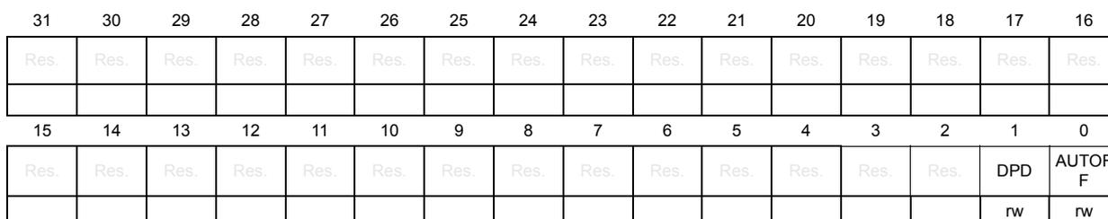
| 31 | 30 | 29 | 28 | 27 | 26 | 25 | 24 | 23 | 22 | 21 | 20 | 19 | 18 | 17 | 16 |
| Res. | Res. | Res. | Res. | Res. | Res. | Res. | Res. | Res. | Res. | Res. | Res. | Res. | Res. | Res. | Res. |
| 15 | 14 | 13 | 12 | 11 | 10 | 9 | 8 | 7 | 6 | 5 | 4 | 3 | 2 | 1 | 0 |
| Res. | Res. | Res. | Res. | Res. | Res. | Res. | Res. | Res. | Res. | Res. | Res. | Res. | Res. | DPD | AUTOFF |
| rw | rw |
Bits 31:2 Reserved, must be kept at reset value.
Bit 1 DPD : Deep-power-down mode bit
This bit is set and cleared by software. It is used to enable/disable Deep-power-down mode in autonomous mode when the ADC is not used.
0: Deep-power-down mode disabled
1: Deep-power-down mode enabled
Note: The software is allowed to write this bit only when ADEN bit is cleared to 0 (this ensures that no conversion is ongoing).
Setting DPD in auto-off mode automatically disables the LDO.
Bit 0 AUTOFF : Auto-off mode bit
This bit is set and cleared by software. it is used to enable/disable the auto-off mode.
0: Auto-off mode disabled
1: Auto-off mode enabled
Note: The software is allowed to write this bit only when ADEN bit is cleared to 0 (this ensures that no conversion is ongoing).
22.7.14 ADC Analog Watchdog 2 Configuration register (ADC_AWD2CR)
Address offset: 0xA0
Reset value: 0x0000 0000
| 31 | 30 | 29 | 28 | 27 | 26 | 25 | 24 | 23 | 22 | 21 | 20 | 19 | 18 | 17 | 16 |
|---|---|---|---|---|---|---|---|---|---|---|---|---|---|---|---|
| Res. | Res. | Res. | Res. | Res. | Res. | Res. | Res. | Res. | Res. | Res. | Res. | Res. | Res. | Res. | Res. |
| 15 | 14 | 13 | 12 | 11 | 10 | 9 | 8 | 7 | 6 | 5 | 4 | 3 | 2 | 1 | 0 |
| Res. | Res. | AWD2 CH13 | AWD2 CH12 | AWD2 CH11 | AWD2 CH10 | AWD2 CH9 | AWD2 CH8 | AWD2 CH7 | AWD2 CH6 | AWD2 CH5 | AWD2 CH4 | AWD2 CH3 | AWD2 CH2 | AWD2 CH1 | AWD2 CH0 |
| rw | rw | rw | rw | rw | rw | rw | rw | rw | rw | rw | rw | rw | rw |
Bits 31:14 Reserved, must be kept at reset value.
Bits 13:0 AWD2CHx : Analog watchdog channel selection (x = 13 to 0)
These bits are set and cleared by software. They enable and select the input channels to be guarded by analog watchdog 2 (AWD2).
0: ADC analog channel-x is not monitored by AWD2
1: ADC analog channel-x is monitored by AWD2
Note: The channels selected through ADC_AWD2CR must be also configured into the ADC_CHSELR registers. Refer to SQ8[3:0] for a definition of channel selection. The software is allowed to write this bit only when ADSTART is cleared to 0 by writing ADSTP to 1 (which ensures that no conversion is ongoing).
22.7.15 ADC Analog Watchdog 3 Configuration register (ADC_AWD3CR)
Address offset: 0xA4
Reset value: 0x0000 0000
| 31 | 30 | 29 | 28 | 27 | 26 | 25 | 24 | 23 | 22 | 21 | 20 | 19 | 18 | 17 | 16 |
|---|---|---|---|---|---|---|---|---|---|---|---|---|---|---|---|
| Res. | Res. | Res. | Res. | Res. | Res. | Res. | Res. | Res. | Res. | Res. | Res. | Res. | Res. | Res. | Res. |
| 15 | 14 | 13 | 12 | 11 | 10 | 9 | 8 | 7 | 6 | 5 | 4 | 3 | 2 | 1 | 0 |
| Res. | Res. | AWD3 CH13 | AWD3 CH12 | AWD3 CH11 | AWD3 CH10 | AWD3 CH9 | AWD3 CH8 | AWD3 CH7 | AWD3 CH6 | AWD3 CH5 | AWD3 CH4 | AWD3 CH3 | AWD3 CH2 | AWD3 CH1 | AWD3 CH0 |
| rw | rw | rw | rw | rw | rw | rw | rw | rw | rw | rw | rw | rw | rw |
Bits 31:14 Reserved, must be kept at reset value.
Bits 13:0 AWD3CHx : Analog watchdog channel selection (x = 13 to 0)
These bits are set and cleared by software. They enable and select the input channels to be guarded by analog watchdog 3 (AWD3).
0: ADC analog channel-x is not monitored by AWD3
1: ADC analog channel-x is monitored by AWD3
Note: The channels selected through ADC_AWD3CR must be also configured into the ADC_CHSELR registers. Refer to SQ8[3:0] for a definition of channel selection. The software is allowed to write this bit only when ADSTART is cleared to 0 by writing ADSTP to 1 (which ensures that no conversion is ongoing).
22.7.16 ADC Calibration factor (ADC_CALFACT)
Address offset: 0xC4
Reset value: 0x0000 0000
| 31 | 30 | 29 | 28 | 27 | 26 | 25 | 24 | 23 | 22 | 21 | 20 | 19 | 18 | 17 | 16 |
|---|---|---|---|---|---|---|---|---|---|---|---|---|---|---|---|
| Res. | Res. | Res. | Res. | Res. | Res. | Res. | Res. | Res. | Res. | Res. | Res. | Res. | Res. | Res. | Res. |
| 15 | 14 | 13 | 12 | 11 | 10 | 9 | 8 | 7 | 6 | 5 | 4 | 3 | 2 | 1 | 0 |
| Res. | Res. | Res. | Res. | Res. | Res. | Res. | Res. | Res. | CALFACT[6:0] | ||||||
| rw | rw | rw | rw | rw | rw | rw | |||||||||
Bits 31:7 Reserved, must be kept at reset value.
Bits 6:0 CALFACT[6:0] : Calibration factor
These bits are written by hardware or by software.
- – Once a calibration is complete, they are updated by hardware with the calibration factors.
- – Software can write these bits with a new calibration factor. If the new calibration factor is different from the current one stored into the analog ADC, it is then applied once a new calibration is launched.
- – Just after a calibration is complete, DATA[6:0] contains the calibration factor.
Note: Software can write these bits only when ADEN = 1 (ADC is enabled and no calibration is ongoing and no conversion is ongoing).
22.7.17 ADC common configuration register (ADC_CCR)
Address offset: 0x308
Reset value: 0x0000 0000
| 31 | 30 | 29 | 28 | 27 | 26 | 25 | 24 | 23 | 22 | 21 | 20 | 19 | 18 | 17 | 16 |
|---|---|---|---|---|---|---|---|---|---|---|---|---|---|---|---|
| Res. | Res. | Res. | Res. | Res. | Res. | Res. | Res. | VSENSE SEL | VREF EN | PRESC[3:0] | Res. | Res. | |||
| rw | rw | rw | rw | rw | rw | ||||||||||
| 15 | 14 | 13 | 12 | 11 | 10 | 9 | 8 | 7 | 6 | 5 | 4 | 3 | 2 | 1 | 0 |
| Res. | Res. | Res. | Res. | Res. | Res. | Res. | Res. | Res. | Res. | Res. | Res. | Res. | Res. | Res. | Res. |
Bits 31:25 Reserved, must be kept at reset value.
Bit 24 Reserved, must be kept at reset value.
Bit 23 VSENSESEL : Temperature sensor selection
This bit is set and cleared by software to enable/disable the temperature sensor.
0: Temperature sensor disabled
1: Temperature sensor enabled
Note: Software is allowed to write this bit only when ADSTART is cleared to 0 by writing ADSTP to 1 (which ensures that no conversion is ongoing).
Bit 22 VREFEN : V REFINT enable
This bit is set and cleared by software to enable/disable the V REFINT buffer.
0: V REFINT disabled
1: V REFINT enabled
Note: Software is allowed to write this bit only when ADSTART is cleared to 0 by writing ADSTP to 1 (which ensures that no conversion is ongoing).
Bits 21:18 PRESC[3:0] : ADC prescaler
Set and cleared by software to select the frequency of the clock to the ADC.
0000: input ADC clock not divided
0001: input ADC clock divided by 2
0010: input ADC clock divided by 4
0011: input ADC clock divided by 6
0100: input ADC clock divided by 8
0101: input ADC clock divided by 10
0110: input ADC clock divided by 12
0111: input ADC clock divided by 16
1000: input ADC clock divided by 32
1001: input ADC clock divided by 64
1010: input ADC clock divided by 128
1011: input ADC clock divided by 256
Other: Reserved
Note: Software is allowed to write these bits only when the ADC is disabled (ADCAL = 0, ADSTART = 0, ADSTP = 0, ADDIS = 0 and ADEN = 0).
Bits 17:0 Reserved, must be kept at reset value.
22.7.18 ADC register map
The following table summarizes the ADC registers.
Table 176. ADC register map and reset values
| Offset | Register name | 31 | 30 | 29 | 28 | 27 | 26 | 25 | 24 | 23 | 22 | 21 | 20 | 19 | 18 | 17 | 16 | 15 | 14 | 13 | 12 | 11 | 10 | 9 | 8 | 7 | 6 | 5 | 4 | 3 | 2 | 1 | 0 | |
|---|---|---|---|---|---|---|---|---|---|---|---|---|---|---|---|---|---|---|---|---|---|---|---|---|---|---|---|---|---|---|---|---|---|---|
| 0x00 | ADC_ISR | Res. | Res. | Res. | Res. | Res. | Res. | Res. | Res. | Res. | Res. | Res. | Res. | Res. | Res. | Res. | Res. | Res. | Res. | Res. | LDORDY | EOCAL | Res. | AWD3 | AWD2 | AWD1 | Res. | Res. | Res. | OVR | EOS | EOC | EOSMP | ADRDY |
| Reset value | 0 | 0 | 0 | 0 | 0 | 0 | 0 | 0 | 0 | 0 | ||||||||||||||||||||||||
| 0x04 | ADC_IER | Res. | Res. | Res. | Res. | Res. | Res. | Res. | Res. | Res. | Res. | Res. | Res. | Res. | Res. | Res. | Res. | Res. | Res. | Res. | LDORDYIE | EOCALIE | Res. | AWD3IE | AWD2IE | AWD1IE | Res. | Res. | Res. | OVRIE | EOSIE | EOCIE | EOSMPIE | ADRDYIE |
| Reset value | 0 | 0 | 0 | 0 | 0 | 0 | 0 | 0 | 0 | 0 | ||||||||||||||||||||||||
| 0x08 | ADC_CR | ADCAL | Res. | Res. | ADVREGEN | Res. | Res. | Res. | Res. | Res. | Res. | Res. | Res. | Res. | Res. | Res. | Res. | Res. | Res. | Res. | Res. | Res. | Res. | Res. | Res. | Res. | Res. | Res. | Res. | ADSTP | Res. | ADSTART | ADDIS | ADEN |
| Reset value | 0 | 0 | 0 | 0 | 0 | 0 | ||||||||||||||||||||||||||||
| 0x0C | ADC_CFGR1 | Res. | AWDCH[4:0] | Res. | Res. | AWD1EN | AWD1SGL | CHSELRMOD | Res. | Res. | Res. | DISCEN | Res. | WAIT | CONT | OVRMOD | EXTEN[1:0] | Res. | EXTSEL[2:0] | Res. | ALIGN | SCANDIR | RES[1:0] | DMACFG | DMAEN | |||||||||
| Reset value | 0 | 0 | 0 | 0 | 0 | 0 | 0 | 0 | 0 | 0 | 0 | 0 | 0 | 0 | 0 | 0 | 0 | 0 | 0 | 0 | 0 | 0 | 0 | |||||||||||
Table 176. ADC register map and reset values (continued)
| Offset | Register name | 31 | 30 | 29 | 28 | 27 | 26 | 25 | 24 | 23 | 22 | 21 | 20 | 19 | 18 | 17 | 16 | 15 | 14 | 13 | 12 | 11 | 10 | 9 | 8 | 7 | 6 | 5 | 4 | 3 | 2 | 1 | 0 |
|---|---|---|---|---|---|---|---|---|---|---|---|---|---|---|---|---|---|---|---|---|---|---|---|---|---|---|---|---|---|---|---|---|---|
| 0x10 | ADC_CFG2 | Res. | Res. | LFTRIG | Res. | Res. | Res. | Res. | Res. | Res. | Res. | Res. | Res. | Res. | Res. | Res. | Res. | Res. | Res. | Res. | Res. | Res. | Res. | TOVS | OVSS[3:0] | OVSR [2:0] | Res. | OVSE | |||||
| Reset value | 0 | 0 | 0 | 0 | 0 | 0 | 0 | 0 | 0 | 0 | |||||||||||||||||||||||
| 0x14 | ADC_SMPR | Res. | Res. | Res. | Res. | Res. | Res. | Res. | Res. | Res. | Res. | SMPSEL13 | SMPSEL12 | SMPSEL11 | SMPSEL10 | SMPSEL9 | SMPSEL8 | SMPSEL7 | SMPSEL6 | SMPSEL5 | SMPSEL4 | SMPSEL3 | SMPSEL2 | SMPSEL1 | SMPSEL0 | Res. | SMP2 [2:0] | Res. | SMP1 [2:0] | ||||
| Reset value | 0 | 0 | 0 | 0 | 0 | 0 | 0 | 0 | 0 | 0 | 0 | 0 | 0 | 0 | 0 | 0 | 0 | 0 | 0 | 0 | |||||||||||||
| 0x18-0x1C | Reserved | Reserved | |||||||||||||||||||||||||||||||
| 0x20 | ADC_AWD1TR | Res. | Res. | Res. | Res. | HT1[11:0] | Res. | Res. | Res. | Res. | LT1[11:0] | ||||||||||||||||||||||
| Reset value | 1 | 1 | 1 | 1 | 1 | 1 | 1 | 1 | 1 | 1 | 1 | 1 | 0 | 0 | 0 | 0 | 0 | 0 | 0 | 0 | 0 | 0 | 0 | 0 | |||||||||
| 0x24 | ADC_AWD2TR | Res. | Res. | Res. | Res. | HT2[11:0] | Res. | Res. | Res. | Res. | LT2[11:0] | ||||||||||||||||||||||
| Reset value | 1 | 1 | 1 | 1 | 1 | 1 | 1 | 1 | 1 | 1 | 1 | 1 | 0 | 0 | 0 | 0 | 0 | 0 | 0 | 0 | 0 | 0 | 0 | 0 | |||||||||
| 0x28 | ADC_CHSELR (CHSELROMOD = 0) | Res. | Res. | Res. | Res. | Res. | Res. | Res. | Res. | Res. | Res. | Res. | Res. | Res. | Res. | Res. | Res. | Res. | Res. | CHSEL13 | CHSEL12 | CHSEL11 | CHSEL10 | CHSEL9 | CHSEL8 | CHSEL7 | CHSEL6 | CHSEL5 | CHSEL4 | CHSEL3 | CHSEL2 | CHSEL1 | CHSEL0 |
| Reset value | 0 | 0 | 0 | 0 | 0 | 0 | 0 | 0 | 0 | 0 | 0 | 0 | 0 | 0 | |||||||||||||||||||
| 0x28 | ADC_CHSELR (CHSELROMOD = 1) | SQ8[3:0] | SQ7[3:0] | SQ6[3:0] | SQ5[3:0] | SQ4[3:0] | SQ3[3:0] | SQ2[3:0] | SQ1[3:0] | ||||||||||||||||||||||||
| Reset value | 0 | 0 | 0 | 0 | 0 | 0 | 0 | 0 | 0 | 0 | 0 | 0 | 0 | 0 | 0 | 0 | 0 | 0 | 0 | 0 | 0 | 0 | 0 | 0 | 0 | 0 | 0 | 0 | 0 | 0 | 0 | 0 | |
| 0x2C | ADC_AWD3TR | Res. | Res. | Res. | Res. | HT3[11:0] | Res. | Res. | Res. | Res. | LT3[11:0] | ||||||||||||||||||||||
| Reset value | 1 | 1 | 1 | 1 | 1 | 1 | 1 | 1 | 1 | 1 | 1 | 1 | 0 | 0 | 0 | 0 | 0 | 0 | 0 | 0 | 0 | 0 | 0 | 0 | |||||||||
| 0x30 - 0x3C | Reserved | Reserved | |||||||||||||||||||||||||||||||
| 0x40 | ADC_DR | Res. | DATA[15:0] | ||||||||||||||||||||||||||||||
| Reset value | 0 | 0 | 0 | 0 | 0 | 0 | 0 | 0 | 0 | 0 | 0 | 0 | 0 | 0 | 0 | 0 | |||||||||||||||||
| 0x44 | ADC_PWRR | Res. | DPD | AUTOFF | |||||||||||||||||||||||||||||
| Reset value | 0 | 0 | |||||||||||||||||||||||||||||||
| 0x48 - 0xBF | Reserved | Reserved | |||||||||||||||||||||||||||||||
| 0xA0 | ADC_AWD2CR | Res. | AWD2CH13 | AWD2CH12 | AWD2CH11 | AWD2CH10 | AWD2CH9 | AWD2CH8 | AWD2CH7 | AWD2CH6 | AWD2CH5 | AWD2CH4 | AWD2CH3 | AWD2CH2 | AWD2CH1 | AWD2CH0 | |||||||||||||||||
| Reset value | 0 | 0 | 0 | 0 | 0 | 0 | 0 | 0 | 0 | 0 | 0 | 0 | 0 | 0 | |||||||||||||||||||
| 0xA4 | ADC_AWD3CR | Res. | AWD3CH13 | AWD3CH12 | AWD3CH11 | AWD3CH10 | AWD3CH9 | AWD3CH8 | AWD3CH7 | AWD3CH6 | AWD3CH5 | AWD3CH4 | AWD3CH3 | AWD3CH2 | AWD3CH1 | AWD3CH0 | |||||||||||||||||
| Reset value | 0 | 0 | 0 | 0 | 0 | 0 | 0 | 0 | 0 | 0 | 0 | 0 | 0 | 0 | |||||||||||||||||||
| 0xA4 - 0xC0 | Reserved | Reserved | |||||||||||||||||||||||||||||||
| 0xC4 | ADC_CALFACT | Res. | CALFACT[6:0] | ||||||||||||||||||||||||||||||
| Reset value | 0 | 0 | 0 | 0 | 0 | 0 | 0 | ||||||||||||||||||||||||||
| 0xB8 - 0xCF | Reserved | Reserved | |||||||||||||||||||||||||||||||
| 0x308 | ADC_CCR | Res. | VSENSESEL | VREFEN | PRESC3 | PRESC2 | PRESC1 | PRESC0 | Res. | ||||||||||||||||||||||||
| Reset value | 0 | 0 | 0 | 0 | 0 | 0 | |||||||||||||||||||||||||||
Refer to Section 2.3: Memory organization for the register boundary addresses.