20. Extended-SPI interface (XSPI)
20.1 XSPI introduction
The XSPI supports external serial memories such as serial NAND and serial NOR flash memories, with the following functional modes:
- • indirect mode: all the operations are performed using the XSPI registers to preset commands, addresses, data, and transfer parameters.
- • memory-mapped mode: the external memory is memory mapped and it is seen by the system as if it was an internal memory, supporting read operations.
The XSPI supports the following protocol with associated frame format:
- • the regular-command frame format with the command, address, alternate byte, dummy cycles, and data phase
20.2 XSPI main features
- • Functional modes: indirect and memory-mapped
- • Read support in memory-mapped mode
- • Support for single, dual, quad, octal communication
- • Dual-memory configuration, where eight bits can be sent/received simultaneously by accessing two quad memories in parallel
- • SDR (single-data rate) and DTR (double-transfer rate) support
- • Data strobe support
- • Fully programmable opcode
- • Fully programmable frame format
- • Integrated FIFO for reception and transmission
- • 8-, 16-, and 32-bit data accesses allowed
- • DMA protocol support
- • DMA channel for indirect mode operations
- • Interrupt generation on FIFO threshold, timeout, operation complete, and access error
- • XSPI interface with transaction acceptance limited to one: the interface accepts the next transfer on AHB bus only once the previous is completed on memory side.
- • Dual chip select support (NCS1 and NCS2)
- • Possibility to disable the automatic prefetch
20.3 XSPI implementation
Table 150. XSPI implementation
| XSPI feature | XSPI1 |
|---|---|
| Octal mode configuration (8-bit) | - |
| Quad mode configuration (4-bit) | X |
| 16-bit mode configuration | - |
Table 150. XSPI implementation (continued)
| XSPI feature | XSPI1 |
|---|---|
| HyperBus standard compliant | - |
| Xccela standard compliant | X |
| XSPI (JESD251C) standard compliant | X |
| AMBA® AHB compliant data interface | X |
| Dual AHB interface | X |
| Asynchronous AHB clock versus kernel clock | - |
| Functional modes: indirect, automatic status-polling, and memory-mapped (1)(2) | X |
| Read and write support in memory-mapped mode (2) | X |
| Dual-quad configuration | - |
| SDR (single-data rate) and DTR (double-transfer rate) | X |
| Data strobe (DS,DQS) | X |
| Fully programmable opcode | X |
| Fully programmable frame format | X |
| Integrated FIFO for reception and transmission | X |
| 8-, 16-, and 32-bit data accesses | X |
| Interrupt on FIFO threshold, timeout, operation complete, and access error | X |
| Bus error bit | - |
| Address offset | - |
| Extended CSHT timeout | X |
| Memory-mapped write | - |
| Refresh counter | - |
| GPDMA interface | X |
| Dual chip select | - |
| Extended external memory | - |
| Prefetch disable | X |
| Prefetch hardware software | - |
1. Automatic status polling mode is not supported.
2. Memory-mapped write are not supported.
20.4 XSPI functional description
20.4.1 XSPI block diagram
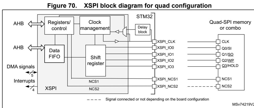
Figure 70. XSPI block diagram for quad configuration
MSv74219V2
20.4.2 XSPI pins and internal signals
Table 151. XSPI input/output pins
| Pin name | Type | Description |
|---|---|---|
| XSPI_CLK | Output | XSPI clock |
| XSPI_IO n (n = 0 to 7) | Input/output | XSPI data pins (1) |
| XSPI_NCS1,2 | Output | Chip select for the memory (2) |
| XSPI_DQS | Input/output | Data strobe/write mask signal from/to the memory |
- 1. XSPI_IO[7:4] is not supported.
- 2. XSPI_NCS2 is not supported.
Caution: Use the same configuration (output speed, HSLV (a) ) for all XSPI input/output pins to avoid any data corruption.
Table 152. XSPI internal signals
| Signal name | Type | Description |
|---|---|---|
| xspi_hclk | Input | XSPI AHB clock |
| xspi_dma | N/A | DMA request signal |
| xspi_it | Output | Global interrupt line (see Table 155 for the multiple sources of interrupt) |
a. When applicable.
20.4.3 XSPI interface to memory modes
The XSPI supports the following protocol:
- • regular-command protocol
The XSPI uses from 6 to 12 signals to interface with a memory, depending on the functional mode:
- • NCS: chip-select (in the following sections, unless otherwise specified, NCS applies for NCS1 or NCS2. Only one of these two signals is active at a given moment in time)
- • CLK: communication clock
- • DQS: data strobe used only in regular-command protocol as input only
- • IO[3:0]: data bus LSB
- • IO[7:4]:
- – data bus MSB used in dual-quad and octal configurations
- – data bus can be used as possible remap for quad-SPI mode
20.4.4 XSPI regular-command protocol
When in regular-command protocol, the XSPI communicates with the external device using commands. Each command can include the following phases:
- • Instruction phase
- • Address phase
- • Alternate-byte phase
- • Dummy-cycle phase
- • Data phase
Any of these phases can be configured to be skipped but, in case of single-phase command, the only use case supported is instruction-phase-only.
The NCS falls before the start of each command and rises again after each command finishes.
In memory-mapped mode, read operations are supported.
Figure 71. SDR read command in octal configuration
![Timing diagram for SDR read command in octal configuration. The diagram shows three signal lines: NCS (chip select), CLK (clock), and IO[7:0] (data bus). NCS is active low and falls before the command starts. CLK is a square wave. IO[7:0] shows the data flow: Instruction phase (ECh, 13h), Address phase (A[31:24], A[23:16], A[15:8], A[7:0]), Dummy phase (Pre-drive), and Data phase (D0, D1, D2, D3). The Address phase is divided into four bytes, and the Data phase shows four bytes being received. The diagram is labeled MSV43488V1.](/RM0521-STM32WBA2/6aa7bc7448897682da2201f18df46006_img.jpg)
The specific regular-command protocol features are configured through the registers in the 0x0100-0x01FC offset range.
Instruction phase
During this phase, a 1- to 4-byte instruction is sent to the external device specifying the type of operation to be performed. The size of the instruction to be sent is configured
by ISIZE[1:0] in XSPI_CCR and the instruction is programmed in INSTRUCTION[31:0] of XSPI_IR.
The instruction phase can optionally send:
- • 1 bit at a time (over IO0, SO signal in single-SPI mode)
- • 2 bits at a time (over IO0/IO1 in dual-SPI mode)
- • 4 bits at a time (over IO0 to IO3 in quad-SPI mode)
- • 8 bits at a time (over IO0 to IO7 in octal-SPI mode)
This can be configured using IMODE[2:0] of XSPI_CCR.
The instruction can be sent in DTR mode on each rising and falling edge of the clock, by setting IDTR in XSPI_CCR.
When IMODE[2:0] = 000 in XSPI_CCR, the instruction phase is skipped, and the command sequence starts with the address phase, if present.
In memory-mapped mode, the instruction used for the read operation and the instruction format are specified in XSPI_IR and XSPI_CCR.
Address phase
In the address phase, 1 to 4 bytes are sent to the external device, to indicate the address of the operation. The number of address bytes to be sent is configured by ADSIZE[1:0] in XSPI_CCR.
In indirect mode, the address bytes to be sent are specified by ADDRESS[31:0] in XSPI_AR. In memory-mapped mode, the address is given directly via the AHB (from any master in the system).
The address phase can send:
- • 1 bit at a time (over IO0, SO signal in single-SPI mode)
- • 2 bits at a time (over IO0/IO1 in dual-SPI mode)
- • 4 bits at a time (over IO0 to IO3 in quad-SPI mode)
- • 8 bits at a time (over IO0 to IO7 in octal-SPI mode)
This can be configured using ADMODE[2:0] in XSPI_CCR.
The address can be sent in DTR mode (on each rising and falling edge of the clock) setting ADDTR in XSPI_CCR.
When ADMODE[2:0] = 000, the address phase is skipped and the command sequence proceeds directly to the next phase, if any.
In memory-mapped mode, the address format for the read operation is specified in XSPI_CCR.
Alternate-byte phase
In the alternate-byte phase, 1 to 4 bytes are sent to the external device, generally to control the mode of operation. The number of alternate bytes to be sent is configured by ABSIZE[1:0] in XSPI_CCR. The bytes to be sent are specified in XSPI_ABR.
The alternate-byte phase can send:
- • 1 bit at a time (over IO0, SO signal in single-SPI mode)
- • 2 bits at a time (over IO0/IO1 in dual-SPI mode)
- • 4 bits at a time (over IO0 to IO3 in quad-SPI mode)
- • 8 bits at a time (over IO0 to IO7 in octal-SPI mode)
This can be configured using ABMODE[2:0] in XSPI_CCR.
The alternate bytes can be sent in DTR mode (on each rising and falling edge of the clock) setting ABDTR in XSPI_CCR.
When ABMODE[2:0] = 000, the alternate-byte phase is skipped and the command sequence proceeds directly to the next phase, if any.
There may be times when only a single nibble needs to be sent during the alternate-byte phase rather than a full byte, such as when the dual-SPI mode is used and only two cycles are used for the alternate bytes.
In this case, the firmware can use the quad-SPI mode (ABMODE[2:0] = 011) and send a byte with bits 7 and 3 of ALTERNATE[31:0] set to 1 (keeping the IO3 line high), and bits 6 and 2 set to 0 (keeping the IO2 line low), in XSPI_IR.
The upper two bits of the nibble to be sent are then placed in bits 5:4 of ALTERNATE[31:0] while the lower two bits are placed in bits 1:0. For example, if the nibble 2 (0010) is to be sent over IO0/IO1, then ALTERNATE[31:0] must be set to 0x8A (1000_1010).
In memory-mapped mode, the alternate bytes used for read operation and the alternate byte format are specified in XSPI_ABR and XSPI_CCR.
Dummy-cycle phase (memory latency)
In the dummy-cycle phase, 1 to 31 cycles are given without any data being sent or received, in order to give the external device, the time to prepare for the data phase when higher clock frequencies are used. The number of cycles given during this phase is specified by DCYC[4:0] in XSPI_TCR. In both SDR and DTR modes, the duration is specified as a number of full CLK cycles.
When DCYC[4:0] = 00000, the dummy-cycle phase is skipped, and the command sequence proceeds directly to the data phase, if present.
In order to assure enough “turn-around” time for changing the data signals from the output mode to the input mode, there must be at least one dummy cycle when using the dual-, the quad-, or the octal-SPI mode, to receive data from the external device.
In memory-mapped mode, the dummy cycles for the read operation are specified in XSPI_TCR.
Data phase
During the data phase, any number of bytes can be sent to or received from the external device.
In indirect mode, the number of bytes to be sent/received is specified in XSPI_DLR. In this mode, the data to be sent to the external device must be written to XSPI_DR, while in indirect-read mode the data received from the external device is obtained by reading XSPI_DR.
In memory-mapped mode, the data read is received directly over the AHB to the Cortex core or to a DMA.
The data phase can send/receive:
- • 1 bit at a time (over IO0/IO1 (SO/SI respectively) in single-SPI mode)
- • 2 bits at a time (over IO0/IO1 in dual-SPI mode)
- • 4 bits at a time (over IO0 to IO3 in quad-SPI mode)
- • 8 bits at a time (over IO0 to IO7 in octal-SPI mode)
This can be configured using DMODE[2:0] in XSPI_CCR.
The data can be sent or received in DTR mode (on each rising and falling edge of the clock) setting DDTR in XSPI_CCR.
When DMODE[2:0] = 000, the data phase is skipped, and the command sequence finishes immediately by raising the NCS. This configuration must be used only in indirect-write mode.
In memory-mapped mode, the data format for the read operation is specified in XSPI_CCR.
DQS use
The DQS signal can be used for data strobing during the read transactions when the device toggles the DQS aligned with the data.
The DQS management can be enabled by setting DQSE in XSPI_CCR.
Figure 72. DTR read in octal-SPI mode with DQS (Macronix mode) example
![Timing diagram for DTR read in octal-SPI mode with DQS. The diagram shows four signals: NCS (active low), CLK (square wave), DQS (data strobe), and IO[7:0] (data bus). The sequence starts with NCS going low, followed by CLK. IO[7:0] sends an address (EEh, 11h, A[31:24], A[23:16], A[15:8], A[7:0]). After a dummy phase (indicated by a hatched area), data is received in word units: D1, D0, D3, D2. DQS is shown toggling to strobe the data. The diagram is labeled MSV43489V1.](/RM0521-STM32WBA2/c6b42f7cc997798b42b06bcd5317c857_img.jpg)
20.4.5 XSPI regular-command protocol signal interface
Single-SPI mode
The legacy SPI mode allows just a single bit to be sent/received serially. In this mode, the data is sent to the external device over the SO signal (Single-SPI Output) (whose I/Os are shared with IO0). The data received from the external device arrives via SI (Single-SPI Input) (whose I/Os are shared with IO1).
Compared to the SPI legacy mode, IO/SO and I1/SI are respectively equivalent to MOSI and MISO, having the XSPI generating the clock.
The different phases can each be configured separately to use this single-SPI mode by setting to 001 the IMODE, ADMODE, ABMODE, and DMODE fields in XSPI_CCR and XSPI_WCCR.
In each phase configured in single-SPI mode:
- • IO0 (SO) is in output mode.
- • IO1 (SI) is in input mode (high impedance).
- • IO2 is in output mode and forced to 0.
- • IO3 is in output mode and forced to 1 (to deactivate the “hold” function).
- • IO4 to IO7 are in output mode and forced to 0.
This is the case even for the dummy phase if DMODE[2:0] = 001.
Dual-SPI mode
In dual-SPI mode, two bits are sent/received simultaneously over the IO0/IO1 signals.
The different phases can each be configured separately to use dual-SPI mode by setting to 010 the IMODE, ADMODE, ABMODE, and DMODE fields in XSPI_CCR and XSPI_WCCR.
In each phase configured in dual-SPI mode:
- • IO0/IO1 are at high-impedance (input) during the data phase for the read operations, and outputs in all other cases.
- • IO2 is in output mode and forced to 0.
- • IO3 is in output mode and forced to 1.
- • IO4 to IO7 are in output mode and forced to 0.
In the dummy phase, when DMODE[2:0] = 010, IO0 and IO1 are in a high-impedance state during read transactions, and are forced to either high or low levels during write transactions.
Quad-SPI mode
In quad-SPI mode, four bits are sent/received simultaneously over the IO0/IO1/IO2/IO3 signals.
The different phases can each be configured separately to use the quad-SPI mode by setting to 011 the IMODE, ADMODE, ABMODE, and DMODE fields in XSPI_CCR and XSPI_WCCR.
In each phase configured in quad-SPI mode:
- • IO0 to IO3 are all at high-impedance (inputs) during the data phase for the read operations, and outputs in all other cases.
- • IO4 to IO7 are in output mode and forced to 0.
In the dummy phase, when DMODE[2:0] = 011, IO0 to IO3 are in a high-impedance state during read transactions, and are forced to either high or low levels during write transactions.
Octal-SPI mode
In regular octal-SPI mode, the eight bits are sent/received simultaneously over the IO[0:7] signals.
The different phases can each be configured separately to use the octal-SPI mode by setting to 100 the IMODE, ADMODE, ABMODE, and DMODE fields in XSPI_CCR and XSPI_WCCR.
In each phase that is configured in octal-SPI mode, IO[0:7] are all at high-impedance (input) during the data phase for read operations, and outputs in all other cases.
In the dummy phase, when DMODE[2:0] = 100, IO[0:7] are in a high-impedance state during read transactions, and are forced to either high or low levels during write transactions.
Single-data rate (SDR) mode
By default, all the phases operate in single-data rate (SDR) mode.
In SDR mode, when the XSPI drives the IO0/SO, IO1 to IO7 signals, these signals transition only with the falling edge of CLK.
When receiving data in SDR mode, the XSPI assumes that the external devices also send the data using CLK falling edge. By default (when SSHIFT = 0 in XSPI_TCR), the signals are sampled using the following (rising) edge of CLK.
Figure 73. SDR write command in octal-SPI mode example
![Timing diagram for SDR write command in octal-SPI mode. The diagram shows three signals: NCS (active low), CLK (square wave), and IO[7:0] (data bus). The sequence of phases is: Instruction (02h), Fake Data (FDh), Address (A[31:24], A[23:16], A[15:8], A[7:0]), Data 0 (D0), Data 1 (D1), Dummy (D254, D255). The NCS signal is low during the entire transaction. The CLK signal is a square wave. The IO[7:0] signal is high-impedance (hatched) during the instruction and address phases, and drives the data during the data and dummy phases. The data is sampled on the rising edge of CLK.](/RM0521-STM32WBA2/9eac14377a049b1a04b63eec3ec06a06_img.jpg)
The diagram illustrates the timing for an SDR write command in octal-SPI mode. The NCS (Negative Clock Signal) line is active-low and remains low throughout the transaction. The CLK (Clock) line is a square wave. The IO[7:0] (Input/Output) bus is shown in three states: high-impedance (indicated by diagonal hatching) during the instruction and address phases, and driving data during the data and dummy phases. The sequence of phases is: Instruction (02h), Fake Data (FDh), Address (divided into four bytes: A[31:24], A[23:16], A[15:8], A[7:0]), Data 0 (D0), Data 1 (D1), and two dummy bytes (D254, D255). Data is driven by the XSPI on the falling edge of CLK and sampled by the external device on the rising edge of CLK.
Double-transfer rate (DTR) mode
Each of the instruction, address, alternate-byte, and data phases can be configured to operate in DTR mode setting IDTR, ADDTR, ABDTR, and DDTR in XSPI_CCR.
In memory-mapped mode, the DTR mode for each phase of the read operations is specified in XSPI_CCR.
In DTR mode, when the XSPI drives the IO0/SO and IO1 to IO7 signals in the instruction, address, and alternate-byte phases, a bit is sent or received on each of the falling and rising edges of CLK.
In DTR mode, when the XSPI drives the IO0 to IO7 signals in the data phases, a bit is sent or received on each of the falling and rising edges of CLK.
When receiving data in DTR mode, the XSPI assumes that the external devices also send the data using both CLK rising and falling edges. When DDTR = 1 in XSPI_CCR, the software must clear SSHIFT in XSPI_TCR. Thus, the signals are sampled one half of a CLK cycle later (on the following, opposite edge).
In DTR mode, it is recommended to set DHQC of XSPI_TCR, to shift the outputs by a quarter of cycle and avoid holding issues on the memory side.
Note: DHQC must not be set when the prescaler value is 0, as this action leads to unpredictable behavior.
Figure 74. DTR write in octal-SPI mode (Macronix mode) example
![Timing diagram for DTR write in octal-SPI mode (Macronix mode) example. The diagram shows three signals: NCS (Active Low Chip Select), CLK (Clock), and IO[7:0] (Data Bus). The NCS signal is active low, starting high, going low for the duration of the transfer, and returning high. The CLK signal is a periodic square wave. The IO[7:0] signal shows the data sequence: a series of dummy cycles (indicated by diagonal hatching), followed by the instruction 02h, the address FDh, and three address segments A[31:24], A[23:16], and A[15:8]. The data phase consists of two 'Word Units'. Each word unit contains two bytes, D1 and D0, followed by D255 and D254. The data is transferred in parallel, with D1 and D255 being the first bytes and D0 and D254 being the second bytes of each word unit. The diagram is labeled MSv43491V1.](/RM0521-STM32WBA2/8f4e98a12762fccee10f1bcbc42bc3f9_img.jpg)
Dual-quad configuration
When DMM = 1 in XSPI_CR, the XSPI is in dual-memory configuration: if DMODE = 011, two external quad-SPI devices (device A and device B) are used in order to send/receive eight bits (or 16 bits in DTR mode) every cycle, effectively doubling the throughput.
Each device (A or B) uses the same CLK and NCS signals, but each has separate IO0 to IO3 signals.
The dual-quad configuration can be used in conjunction with the single-SPI, dual-SPI, and quad-SPI modes, as well as with either the SDR or DTR mode.
The device size, as specified by DEVSIZE[4:0] in XSPI_DCR1, must reflect the total external device capacity that is the double of the size of one individual component.
If address X is even, then the byte that the XSPI gives for address X is the byte at the address X/2 of device A, and the byte that the XSPI gives for address X + 1 is the byte at the address X/2 of device B. In other words, the bytes at even addresses are all stored in device A and the bytes at odd addresses are all stored in device B.
When reading the status registers of the devices in dual-quad configuration, twice as many bytes must be read compared to the same read in regular-command protocol: if each device gives eight valid bits after the instruction for fetching the status register, then the XSPI must be configured with a data length of 2 bytes (16 bits), and the XSPI receives one byte from each device.
If each device gives a status of 16 bits, then the XSPI must be configured to read 4 bytes to get all the status bits of both devices in dual-quad configuration. The least-significant byte of the result (in the data register) is the least-significant byte of device A status register. The next byte is the least-significant byte of device B status register. Then, the third byte of the data register is the device A second byte. The fourth byte is the device B second byte (if devices have 16-bit status registers).
An even number of bytes must always be accessed in dual-quad configuration. For this reason, bit 0 of DL[31:0] in XSPI_DLR is stuck at 1 when DMM = 1.
In dual-quad configuration, the behavior of device A interface signals is basically the same as in normal mode. Device B interface signals have exactly the same waveforms as device A ones during the instruction, address, alternate-byte, and dummy-cycle phases. In other words, each device always receives the same instruction and the same address.
Then, during the data phase, the AIOx and the BIOx buses both transfer data in parallel, but the data that is sent to (or received from) device A is distinct than the one from device B.
20.4.6 XSPI operating mode introduction
The XSPI has the following operating modes regardless of the low-level protocol used :
- • indirect mode (read or write)
- • memory-mapped mode
20.4.7 XSPI indirect mode
In indirect mode, the commands are started by writing to the XSPI registers, and data are transferred by writing or reading the data register, in a similar way to other communication peripherals.
When FMODE[1:0] = 00 in XSPI_CR, the XSPI is in indirect-write mode: bytes are sent to the external device during the data phase. Data are provided by writing to XSPI_DR.
When FMODE[1:0] = 01, the XSPI is in indirect-read mode: bytes are received from the external device during the data phase. Data are recovered by reading XSPI_DR.
In indirect mode, when the XSPI is configured in DTR mode over eight lanes with DQS disabled, the given starting address and the data length must be even.
Note: The XSPI_AR register must be updated even if the start address is the same as the start address of the previous indirect access.
The number of bytes to be read/written is specified in XSPI_DLR:
- • If DL[31:0] = 0xFFFF FFFF, the data length is considered undefined and the XSPI simply continues to transfer data until it reaches the end of the external device (as defined by DEVSIZE). If no bytes are to be transferred, DMODE[2:0] must be set to 0 in XSPI_CCR.
- • If DL[31:0] = 0xFFFF FFFF and DEVSIZE[4:0] = 0x1F (its maximum value indicating at 4-Gbyte device), the transfers continue indefinitely, stopping only after an abort request or after the XSPI is disabled. After the last memory address is read (at address 0xFFFF FFFF), reading continues with address = 0x0000 0000.
When the programmed number of bytes to be transmitted or received is reached, the TCF bit is set in XSPI_SR, and an interrupt is generated if TCIE = 1 in XSPI_CR. In the case of an undefined number of data, TCF is set when the limit of the external SPI memory is reached, according to the device size defined in XSPI_DCR1.
Triggering the start of a transfer in regular-command protocol
Depending on the XSPI configuration, there are three different ways to trigger the start of a transfer in indirect mode when using the regular-command protocol. In general, the start of transfer is triggered as soon as the software gives the last information that is necessary for
the command. More specifically in indirect mode, a transfer starts when one of the following sequence of events occurs:
- • if no address is necessary (ADMODE[2:0] = 000) and if no data need to be provided by the software (FMODE[1:0] = 01 or DMODE[2:0] = 000), and at the moment when a write is performed to INSTRUCTION[31:0] in XSPI_IR
- • if an address is necessary (when ADMODE[2:0] \( \neq \) 000) and if no data need to be provided by the software (when FMODE[1:0] = 01 or DMODE[2:0] = 000), and at the moment when a write is performed to ADDRESS[31:0] in XSPI_AR
- • if data need to be provided by the software (when FMODE[1:0] = 00 and DMODE[2:0] \( \neq \) 000), and at the moment when a write is performed to DATA[31:0] in XSPI_DR
A write to XSPI_ABR never triggers the communication start. If alternate bytes are required, they must have been programmed before.
As soon as a command is started, the BUSY bit is automatically set in XSPI_SR.
FIFO and data management
Data in indirect mode pass through a 32-byte FIFO that is internal to the XSPI. FLEVEL in XSPI_SR indicates how many bytes are currently being held in the FIFO.
AHB burst transactions are supported. Data of the burst are successively written in XSPI_DR, and immediately transferred in the internal FIFO.
In indirect-write mode (FMODE[1:0] = 00), the software adds data to the FIFO when it writes in XSPI_DR. A word write adds 4 bytes to the FIFO, a half-word write adds 2 bytes, and a byte write adds only 1 byte. If the software adds too many bytes to the FIFO (more than indicated in DL[31:0]), the extra bytes are flushed from the FIFO at the end of the write operation (when TCF is set).
The byte/half-word accesses to XSPI_DR must be done only to the least significant byte/halfword of the 32-bit register.
FTHRES is used to define a FIFO threshold after which point the FIFO threshold flag, FTF, gets set. In indirect-read mode, FTF is set when the number of valid bytes to be read from the FIFO is above the threshold. FTF is also set if there is any data left in the FIFO after the last byte is read from the external device, regardless of FTHRES setting. In indirect-write mode, the FTF is set when the number of empty bytes in the FIFO is above the threshold.
If FTIE = 1, there is an interrupt when the FTF is set. If DMAEN = 1, a DMA transfer is initiated when the FTF is set. The FTF is cleared by hardware as soon as the threshold condition is no longer true (after enough data has been transferred by the CPU or DMA).
The last data read in RX FIFO remains valid as long as there is no request for the next line. This means that, when the application reads several times in a row at the same location, the data is provided from the RX FIFO and not read again from the distant memory.
20.4.8 XSPI memory-mapped mode
When configured in memory-mapped mode, the external SPI device is seen as an internal memory.
Note: No more than 256 Mbytes can be addressed even if the external device capacity is larger.
If an access is made to an address outside of the range defined by DEVSIZE[4:0] but still within the 256-Mbyte range, then an AHB error is given. The effect of this error depends on the AHB master that attempted the access:
- • If it is the Cortex CPU, a hard-fault interrupt is generated.
- • If it is a DMA, a DMA transfer error is generated, and the corresponding DMA channel is automatically disabled.
Byte, half-word, and word access types are all supported.
A support for execute in place (XIP) operation is implemented, where the XSPI continues to load the bytes to the addresses following the most recent access. If subsequent accesses are continuous to the bytes that follow, then these operations end up quickly since their results were prefetched.
By default, the XSPI never stops its prefetch operation. It either keeps the previous read operation active with the NCS maintained low or it relaunches a new transfer, even if no access to the external device occurs for a long time. This prefetch feature can be disabled by setting the NOPREF bit in XSPI_DCR1. Disabling the prefetch can be beneficial for performance when the transfer requests are short and jumping frequently between non-consecutive addresses.
Since external devices tend to consume more power when the NCS is held low, the application may want to activate the timeout counter (TCEN = 1 in XSPI_CR): the NCS is released after a period defined by TIMEOUT[15:0] in XSPI_LPTR, when x cycles have elapsed without access since the clock is inactive.
BUSY goes high as soon as the first memory-mapped access occurs. Because of the prefetch operations, BUSY does not fall until there is an abort, or the peripheral is disabled.
It is recommended to add a synchronization barrier between the end of the controller registers configuration and the first memory-mapped access to the external memory when the controller is configured in memory-mapped mode.
The controller can apply an automatic address offset to simplify memory area code switching, such as during a firmware update (if the address offset feature is available in the product implementation table). To enable this feature, set the ADOFFEN bit in the XSPI_CR register and configure the offset value in the ADOFF[4:0] bitfield of the XSPI_DCR1 register. The offset is modulo 256 bytes.
20.4.9 XSPI configuration introduction
The XSPI configuration is done in three steps:
- 1. XSPI system configuration
- 2. XSPI device configuration
- 3. XSPI mode configuration
20.4.10 XSPI system configuration
The XSPI is configured using XSPI_CR. The user must program:
- • the functional mode with FMODE[1:0]
- • the FIFO level with FTHRES
- • the DMA use with DMAEN
- • the timeout counter use with TCEN
- the dual-memory configuration, if needed, with DMM
In case of an interrupt use, the respective enable bit can also be set during this phase.
If the timeout counter is used, the timeout value is programmed in XSPI_LPTR.
The DMA channel must not be enabled during the XSPI configuration: it must be enabled only when the operation is fully configured, to avoid any unexpected request generation.
The DMA and XSPI must be configured in a coherent manner regarding data length: FTHRES value must reflect the DMA burst size.
20.4.11 XSPI device configuration
The parameters related to the external device targeted are configured through XSPI_DCR1 and XSPI_DCR2. The user must program:
- the device size with DEVSIZE[4:0]
- the chip-select minimum high time with CSHT[5:0]
- the clock mode with FRCK and CKMODE
- the associated delay block DLYB connected externally to the peripheral
- the device frequency with PRESCALER[7:0]
DEVSIZE[4:0] defines the size of external memory using the following formula:
where DEVSIZE+1 is the number of address bits required to address the external device. The external device capacity can go up to 4 Gbytes (addressed using 32 bits) in indirect mode, but the addressable space in memory-mapped mode is limited to 256 Mbytes.
If DMM = 1, DEVSIZE[4:0] must reflect the total capacity of the two devices together considering the above formula (DEVSIZE[4:0] value is so equal to one of the two memory capacities).
When the XSPI executes two commands, one immediately after the other, it raises the chip-select signal (NCS) high between the two commands for at least one CLK cycle by default.
If the external device requires more time between commands, CSHT[5:0] can be used to specify the minimum number of CLK cycles for which the NCS must remain high.
CKMODE indicates the level that the CLK takes between commands (when NCS = 1).
Memory types
External memory providers may present some architecture and slight data formatting differences between them. The bitfield MTYP[2:0] into the XSPI_CR register allows targeting the right controller configuration depending on the associated memory type selected in the application. This is the responsibility of the software developer to align the controller configuration to fit with the targeted memory type.
The memory types are grouped in a such way:
- D0/D1 data ordering in octal-SPI data mode (DMODE[2:0] = 100) in DTR mode by configuring MTYP[2:0] = 000. For instance, Micron is using such data ordering. In this configuration, the DQS is sent with a polarity inverted respect to the clock polarity.
Figure 75. D0/D1 data ordering in octal-SPI DTR mode (Micron) - Read access
![Timing diagram for Figure 75 showing NCS, CLK, DQS, and IO[7:0] signals. The diagram illustrates a read access sequence in octal-SPI DTR mode. NCS is active low. CLK is a periodic square wave. DQS is a data strobe signal. IO[7:0] shows the data flow: an initial shaded area, followed by EEh, 11h, A31:24, A23:16, A15:8, A7:0 (labeled 'Address'), a shaded area (labeled 'Dummy'), and then four data units D0, D1, D2, D3 (labeled 'Word unit'). The diagram is labeled MSv71558V1.](/RM0521-STM32WBA2/3a0edcfc38e4b2f1e46273d50ddd188a_img.jpg)
- • D1/D0 data ordering in octal-SPI data mode (DMODE[2:0] = 100) in DTR mode by configuring MTYP[2:0] = 001. For instance, Macronix is using this reverse data ordering in its Octaflash portfolio (this configuration is not adapted to its OctaRAM™ memories). DQS is keeping the same polarity as the clock when reading data from the memory. Refer to Figure 72: DTR read in octal-SPI mode with DQS (Macronix mode) example .
- • D1/D0 data ordering in octal-SPI data mode (DMODE[2:0] = 100) in DTR mode by configuring MTYP[2:0] = 011 with specific address phase built with row and column to fit with Macronix OctaRAM™ memories requirement (refer to Table 153: OctaRAM command address bit assignment (based on 64 Mb OctaRAM) ). This is the controller which translates internally the targeted address provided by the software in row/column address formatting to sent to the memory. DQS is keeping the same polarity as the clock one when reading data from the memory.
Figure 76. OctaRAM read operation with reverse data ordering D1/D0
![Timing diagram for Figure 76 showing NCS, CLK, DQS, and IO[7:0] signals. The diagram illustrates an OctaRAM read operation with reverse data ordering. NCS is active low. CLK is a periodic square wave. DQS is a data strobe signal. IO[7:0] shows the data flow: an initial shaded area, followed by Command, Raw address, and Column address (labeled 'Command & Address'), a shaded area, and then four data units D1, D0, D3, D2 (labeled 'Word Unit'). The diagram is labeled MSv71560V1.](/RM0521-STM32WBA2/4d51cbffacf0c26cdd44ae8ca2a54295_img.jpg)
Table 153. OctaRAM command address bit assignment
(based on 64 Mb
(1)
OctaRAM)
| Clock | 1st clock | 2nd clock | 3rd clock | ||
|---|---|---|---|---|---|
| Function | Command | Row address | Column address | ||
| SIO[7] | Command | Reserved | RA7 | CA9 | Reserved |
| SIO[6] | Reserved | RA6 | CA8 | Reserved | |
| SIO[5] | Reserved | RA5 | CA7 | Reserved | |
| SIO[4] | RA12 | RA4 | CA6 | Reserved | |
| SIO[3] | RA11 | RA3 | CA5 | CA3 | |
| SIO[2] | RA10 | RA2 | CA4 | CA2 | |
| SIO[1] | RA9 | RA1 | Reserved | CA1 | |
| SIO[0] | RA8 | RA0 | Reserved | CA0 (2) | |
- 1. Example of 64 Mb OctaRAM address assignment:
Row Address [RA12:RA0]: 8K. Column Address [CA9:CA0]: 1K. 64 Mb density = 8K x 1K x 8 bits - 2. Column address A0 must be always 0.
- • Standard mode. It is the mode to use whenever the targeted memory is not corresponding to any other configurations described in this section. MTYP[2:0] = 010 for this standard mode.
20.4.12 XSPI regular-command mode configuration
Indirect mode configuration
When FMODE[1:0] = 00, the indirect-write mode is selected and data can be sent to the external device. When FMODE[1:0] = 01, the indirect-read mode is selected, and data can be read from the external device.
When the XSPI is used in indirect mode, the frames are constructed in the following way:
- 1. Specify a number of data bytes to read or write in XSPI_DLR.
- 2. Specify the frame timing in XSPI_TCR.
- 3. Specify the frame format in XSPI_CCR.
- 4. Specify the instruction in XSPI_IR.
- 5. Specify the optional alternate byte to be sent right after the address phase in XSPI_ABR.
- 6. Specify the targeted address in XSPI_AR.
- 7. Enable the DMA channel if needed.
- 8. Read/write the data from/to the FIFO through XSPI_DR (if no DMA usage).
If neither the address register (XSPI_AR) nor the data register (XSPI_DR) need to be updated for a particular command, then the command sequence starts as soon as XSPI_IR is written. This is the case when both ADMODE[2:0] and DMODE[2:0] equal 000, or if just ADMODE[2:0] = 000 when in indirect-read mode (FMODE[1:0] = 01).
When an address is required (ADMODE[2:0] ≠ 000) and the data register does not need to be written (FMODE[1:0] = 01 or DMODE[2:0] = 000), the command sequence starts as soon as the address is updated with a write to XSPI_AR.
In case of data transmission (FMODE[1:0] = 00 and DMODE[2:0] ≠ 000), the communication start is triggered by a write in the FIFO through XSPI_DR.
Memory-mapped mode configuration
In memory-mapped mode, the external device is seen as an internal memory but with some latency during accesses. Read operations are allowed to the external device in this mode.
The memory-mapped mode is entered by setting FMODE[1:0] = 11 in XSPI_CR.
The programmed instruction and frame are sent when an AHB master accesses the memory-mapped space.
The FIFO is used as a prefetch buffer to anticipate any linear reads. Any access to XSPI_DR in this mode returns zero.
The data length register (XSPI_DLR) has no meaning in memory-mapped mode.
When the XSPI is used in memory-mapped mode, the frames are constructed in the following way:
- 1. Specify the frame timing in XSPI_TCR for read operation.
- 2. Specify the frame format in XSPI_CCR for read operation.
- 3. Specify the instruction in XSPI_IR.
- 4. Specify the optional alternate byte to be sent right after the address phase in XSPI_ABR for read operation.
All configuration operations must be completed (ensured by checking BUSY = 0) before the first access to the memory area: any register write operation when BUSY = 1 has no effect and is not signaled with an error response. On the first access, the XSPI becomes busy, and no further configuration is allowed. Then, the only way to get BUSY low is to clear the ENABLE bit or to abort by setting the ABORT bit.
XSPI delayed data sampling when no DQS is used
By default, when no DQS is used, the XSPI samples the data driven by the external device one half of a CLK cycle after the external device drives the signal.
In case of any external signal delays, it may be useful to sample the data later. Using SSHIFT in XSPI_TCR, the sampling of the data can be shifted by half of a CLK cycle.
The firmware must clear SSHIFT when the data phase is configured in DTR mode (DDTR = 1).
XSPI delayed data sampling when DQS is used
When external DQS is used as a sampling clock, it is shifted precisely by one quarter of the SPI clock cycle, for all frequencies above freq_min, to compensate the data propagation delay in the “high-speed interface” when the product embeds one.
This shift is performed by an external delay block (DLYB) located outside the XSPI. This external delay block has to be calibrated (by enabling FRCK) before starting the first transfer, and recalibrated regularly. The control of this feature depends on the device implementation (see the delay block (DLYB) section in this document for more details about DLYB and calibration procedure, and the product datasheet for freq_min value).
In configurations where delay does not need to be compensated, the external delay block can be bypassed by setting DLYBYP in XSPI_DCR1.
20.4.13 XSPI error management
The following errors set the TEF flag in XSPI_SR and generates an interrupt if enabled (TEIE = 1 in XSPI_CR):
- • in indirect mode, when a wrong address has been programmed in XSPI_AR (according to the device size defined by DEVSIZE[4:0]).
- • in indirect mode, if the address plus the data length exceed the device size: TEF is set as soon as the access is triggered.
In memory-mapped mode, the XSPI generates an AHB slave error in the following situations, setting the BERRF flag in XSPI_SR and generating an interrupt if enabled (BERRIE = 1 in XSPI_CR) (if the Bus error bit feature is available in the product implementation table, otherwise the Slave bus error response is generated at system level as transaction response with no dedicated bit into the controller status register):
- • The memory-mapped mode is disabled and an AHB read or write request occurs.
- • A read (including the address offset if ADOFFEN bit is set) address exceeds the size of the external memory.
- • An abort is received while a read burst is ongoing when the abort condition is present at the moment of transfer phases preceding the data phase (In incremental). To avoid the error, refer to Section 20.4.14: XSPI BUSY and ABORT .
- • The XSPI is disabled while a read burst is requested.
- • A read request is received while DMODE[2:0] = 000 (no data phase).
- • Bit DMM is set in XSPI_CR (dual-memory configuration) and octal mode is set.
- • A write request is received.
20.4.14 XSPI BUSY and ABORT
Once the XSPI starts an operation with the external device, BUSY is automatically set in XSPI_SR.
In indirect mode, BUSY is reset once the XSPI has completed the requested command sequence and the FIFO is empty.
After the first access in memory-mapped mode, BUSY goes low only on an abort.
Any operation can be aborted by setting ABORT in XSPI_CR. Once the abort is completed, BUSY and ABORT are automatically reset, and the FIFO is flushed.
Before setting ABORT, the software must ensure that all the current transactions are finished using the synchronization barriers. When DMA is enabled to handle the data read or write operations in XSPI_DR, it is recommended to disable the DMA channel before aborting the SPI.
Note: Some devices may misbehave if a write operation to a status register is aborted.
20.4.15 XSPI reconfiguration or deactivation
Before any XSPI reconfiguration, the software must ensure that all the transactions are completed:
- • After a memory-mapped read, the software must perform a synchronization barrier than an abort.
20.4.16 NCS behavior
By default, NCS is high, deselecting the external device. NCS falls before an operation begins and rises as soon as it finishes.
When CKMODE = 0 (clock mode 0: CLK stays low when no operation is in progress), NCS falls one CLK cycle before an operation first rising CLK edge, and NCS rises one CLK cycle after the operation final rising CLK edge (see the figure below).
Figure 77. NCS when CKMODE = 0 (T = CLK period)
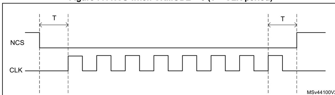
The diagram shows two waveforms: NCS (top) and CLK (bottom). The CLK signal is a periodic square wave with a period labeled 'T'. The NCS signal is initially high. It falls one CLK cycle before the first rising edge of the CLK signal. It remains low through several rising edges of the CLK signal. After the final rising edge of the CLK signal, the NCS signal rises one CLK cycle later. Vertical dashed lines mark the rising edges of the CLK signal. The label 'MSV44100V2' is in the bottom right corner.
Note: Clock mode 3 is not supported.
In dual-memory configuration, the NCS2 behaves exactly the same as the NCS1. The quad-SPI/octal-SPI memory 2 can then use the NCS1, and the NCS2 pin can be used for other functions.
20.4.17 Software control of two external memories
One XSPI instance is able to control the generation of the two chip-select signals (NCS1 and NCS2). This allows two external memories to be connected to the same I/O port driven by the XSPI.
The XSPI generates one NCS signal and the user defines how the NCS is directed to NCS1 or NCS2, by setting the CSSEL bit in XSPI_CR. Intended operation is semistatic commutation, such as starting an application reading an external flash memory and then, for the rest of the application, use an external SRAM connected to the same I/O bus.
From a memory-map point of view, these two memories are located in the same address range.
Figure 78. Example of software control of two external memories (octal mode)
![Diagram showing an XSPI controller connected to two external memories (Memory 1 and Memory 2) in octal mode. The XSPI block has pins for CLK, NCLK, DQS, NCS1, NCS2, and IO[7:0]. Memory 1 and Memory 2 each have pins for clk, nclk, Data strobe, NCS, and Data[7:0]. The XSPI block contains a CSSEL in XSPI_CR register. A 'Software control' arrow points to the CSSEL in XSPI_CR register. The diagram shows the XSPI controller connected to two external memories. The XSPI block has pins for CLK, NCLK, DQS, NCS1, NCS2, and IO[7:0]. Memory 1 and Memory 2 each have pins for clk, nclk, Data strobe, NCS, and Data[7:0]. The XSPI block contains a CSSEL in XSPI_CR register. A 'Software control' arrow points to the CSSEL in XSPI_CR register. The diagram shows the XSPI controller connected to two external memories. The XSPI block has pins for CLK, NCLK, DQS, NCS1, NCS2, and IO[7:0]. Memory 1 and Memory 2 each have pins for clk, nclk, Data strobe, NCS, and Data[7:0]. The XSPI block contains a CSSEL in XSPI_CR register. A 'Software control' arrow points to the CSSEL in XSPI_CR register.](/RM0521-STM32WBA2/d81c682e2efe3c4bc1bb7ef872e47467_img.jpg)
(1): - XXX = XSPI when there is no IO manager in the product
- XXX = XSPIM_Px when an IO manager is available in the product
(2): Refer to the product datasheet for pin availability.
MSv74222V2
20.5 Address alignment and data number
The table below summarizes the effect of the address alignment and programmed data number depending on the use case.
Table 154. Address alignment cases
| Memory type | Transaction type | Constraint on address (1) | Impact if constraint on address not respected | Constraint on number of bytes (1) | Impact if constraint on bytes not respected |
|---|---|---|---|---|---|
| Single, dual, quad flash or SRAM (DMM = 0) | IND (2) read | None | None | None | None |
| MM (3) read | |||||
| IND write | |||||
| Single, dual, quad flash or SRAM (DMM = 1) | IND read | Even | ADDR[0] is set to 0. (4) | Even | DLR[0] is set to 1. (5) |
| MM read | None | None | None | None | |
| IND write | Even | ADDR[0] is set to 0. (4) | Even | DLR[0] is set to 1. (5) | |
| Octal flash in SDR mode | IND read | None | None | None | None |
| MM read | |||||
| IND write | |||||
| Octal memory in DTR mode without WDM (6) | IND read | Even | ADDR[0] is set to 0. (4) | Even | DLR[0] is set to 1. (5) |
| MM read | None | None | None | None | |
| IND write | Even | ADDR[0] is set to 0. (4) | Even | DLR[0] is set to 1. (5) | |
| Octal flash or RAM in DTR mode with WDM | IND read | Even | ADDR[0] is set to 0. (4) | Even | DLR[0] is set to 1. (5) |
| MM read | None | None | None | None | |
| IND write (7) |
1. To be respected by the software.
2. IND = indirect mode.
- 3. MM = memory-mapped mode.
- 4. Extra data at transfer start.
- 5. Extra data at transfer end.
- 6. WDM = write data mask.
- 7. If the FTHRES bitfield is set to the maximum value with DLR value greater than the data burst length, and if the DMA is enabled or the interrupt based on FIFO THRESHOLD Flag is enabled (FTF), the address must be modulo 2 aligned in DTR mode when the initiator (DMA, CPU, ...) is writing the data with a burst length equal to the FIFO size.
20.6 XSPI interrupts
An interrupt can be produced on the following events:
- • Timeout
- • FIFO threshold
- • Transfer complete
- • Transfer error
Separate interrupt enable bits are available to provide more flexibility.
Table 155. XSPI interrupt requests
| Interrupt event | Event flag | Enable control bit |
|---|---|---|
| Timeout | TOF | TOIE |
| FIFO threshold | FTF | FTIE |
| Transfer complete | TCF | TCIE |
| Transfer error | TEF | TEIE |
20.7 XSPI registers
20.7.1 XSPI control register (XSPI_CR)
Address offset: 0x000
Reset value: 0x0000 0000
| 31 | 30 | 29 | 28 | 27 | 26 | 25 | 24 | 23 | 22 | 21 | 20 | 19 | 18 | 17 | 16 |
|---|---|---|---|---|---|---|---|---|---|---|---|---|---|---|---|
| Res. | MSEL | FMODE[1:0] | Res. | Res. | NOPREF | CSSEL | Res. | Res. | BERRIE | TOIE | Res. | FTIE | TCIE | TEIE | |
| rw | rw | rw | rw | rw | rw | rw | rw | rw | |||||||
| 15 | 14 | 13 | 12 | 11 | 10 | 9 | 8 | 7 | 6 | 5 | 4 | 3 | 2 | 1 | 0 |
| Res. | Res. | Res. | FTHRES[4:0] | Res. | DMM | Res. | ADOFFEN | TCEN | DMAEN | ABORT | EN | ||||
| rw | rw | rw | rw | rw | rw | rw | rw | rw | rw | rw | |||||
Bit 31 Reserved, must be kept at reset value.
Bit 30 MSEL : External memory select
This bit selects the external memory to be addressed in single-, dual-, quad-SPI mode in single-memory configuration (when DMM = 0).
0: External memory 1 selected (data exchanged over IO[3:0])
1: External memory 2 selected (data exchanged over IO[7:4])
This bit is ignored when DMM = 1 or when octal-SPI mode is selected.
Note: This bitfield can be modified only when BUSY = 0.
Bits 29:28 FMODE[1:0] : Functional mode
This bitfield defines the XSPI functional mode of operation.
00: Indirect-write mode
01: Indirect-read mode
10: No action derived from this setting
11: Memory-mapped mode
If DMAEN = 1 already, then the DMA controller for the corresponding channel must be disabled before changing the FMODE[1:0] value.
Note: This bitfield can be modified only when BUSY = 0.
Bits 27:26 Reserved, must be kept at reset value.
Bit 25 NOPREF : No prefetch data
This bit disables the automatic prefetch in the external memory.
0: Automatic prefetch enabled
1: Automatic prefetch disabled
Bit 24 CSSEL : Chip-select selection
This bit indicates if it must copy NCS to NCS1 or NCS2.
0: NCS1 active
1: NCS2 active
Note: This bit can be modified only when BUSY = 0.
Bits 23:22 Reserved, must be kept at reset value.
Bit 21 BERRIE : Bus error interrupt enable
This bit enables the bus error interrupt (if Bus error bit feature is available in the product implementation table).
0: Interrupt disabled
1: Interrupt enabled
Bit 20 TOIE : Timeout interrupt enable
This bit enables the timeout interrupt.
0: Interrupt disabled
1: Interrupt enabled
Bit 19 Reserved, must be kept at reset value.
Bit 18 FTIE : FIFO threshold interrupt enable
This bit enables the FIFO threshold interrupt.
0: Interrupt disabled
1: Interrupt enabled
Bit 17 TCIE : Transfer complete interrupt enable
This bit enables the transfer complete interrupt.
0: Interrupt disabled
1: Interrupt enabled
Bit 16 TEIE : Transfer error interrupt enable
This bit enables the transfer error interrupt.
0: Interrupt disabled
1: Interrupt enabled
Bits 15:13 Reserved, must be kept at reset value.
Bits 12:8 FTHRES[4:0] : FIFO threshold level
This bitfield defines, in indirect mode, the threshold number of bytes in the FIFO that causes the FIFO threshold flag FTF in XSPI_SR, to be set.
00000: FTF is set if there are one or more free bytes available to be written to in the FIFO in indirect-write mode, or if there are one or more valid bytes can be read from the FIFO in indirect-read mode.
00001: FTF is set if there are two or more free bytes available to be written to in the FIFO in indirect-write mode, or if there are two or more valid bytes can be read from the FIFO in indirect-read mode.
...
11111: FTF is set if there are 32 free bytes available to be written to in the FIFO in indirect-write mode, or if there are 32 valid bytes can be read from the FIFO in indirect-read mode.
Note: If DMAEN = 1, the DMA controller for the corresponding channel must be disabled before changing the FTHRES[4:0] value.
Bit 7 Reserved, must be kept at reset value.
Bit 6 DMM : Dual-memory configuration
This bit activates the dual-memory configuration, where two external devices are used simultaneously to double the throughput and the capacity
0: Dual-memory configuration disabled
1: Dual-memory configuration enabled
Note: This bit can be modified only when BUSY = 0.
Bit 5 Reserved, must be kept at reset value.
Bit 4 ADOFFEN : Address offset enable
An offset may be applied on the memory address. The offset value is set into ADOFF[4:0].
0: Address offset disabled
1: Address offset enabled
Note: This bit can be modified only when BUSY = 0. This bit is present only if the address offset feature is available in the product implementation table.
Bit 3 TCEN : Timeout counter enable
This bit is valid only when the memory-mapped mode (FMODE[1:0] = 11) is selected. This bit enables the timeout counter.
0: The timeout counter is disabled, and thus the chip-select (NCS) remains active indefinitely after an access in memory-mapped mode.
1: The timeout counter is enabled, and thus the chip-select is released in the memory-mapped mode after TIMEOUT[15:0] cycles of external device inactivity.
Note: This bit can be modified only when BUSY = 0.
Bit 2 DMAEN : DMA enable
In indirect mode, the DMA can be used to input or output data via XSPI_DR. DMA transfers are initiated when FTF is set.
0: DMA disabled for indirect mode
1: DMA enabled for indirect mode
Note: Resetting the DMAEN bit while a DMA transfer is ongoing, breaks the handshake with the DMA. Do not write this bit during DMA operation.
Bit 1 ABORT : Abort request
This bit aborts the ongoing command sequence. It is automatically reset once the abort is completed. This bit stops the current transfer.
0: No abort requested
1: Abort requested
Note: This bit is always read as 0.
Bit 0 EN : Enable
This bit enables the XSPI.
0: XSPI disabled
1: XSPI enabled
Note: The DMA request can be aborted without having received the ACK in case this EN bit is cleared during the operation.
In case this bit is set to 0 during a DMA transfer, the REQ signal to DMA returns to inactive state without waiting for the ACK signal from DMA to be active.
20.7.2 XSPI device configuration register 1 (XSPI_DCR1)
Address offset: 0x008
Reset value: 0x0000 0000
This register can be modified only when BUSY = 0.
| 31 | 30 | 29 | 28 | 27 | 26 | 25 | 24 | 23 | 22 | 21 | 20 | 19 | 18 | 17 | 16 |
|---|---|---|---|---|---|---|---|---|---|---|---|---|---|---|---|
| ADOFF[4:0] | MTYP[2:0] | Res. | Res. | Res. | DEVSIZE[4:0] | ||||||||||
| rw | rw | rw | rw | rw | rw | rw | rw | rw | rw | rw | rw | rw | |||
| 15 | 14 | 13 | 12 | 11 | 10 | 9 | 8 | 7 | 6 | 5 | 4 | 3 | 2 | 1 | 0 |
| Res. | Res. | CSHT[5:0] | Res. | Res. | Res. | Res. | DLYBYP | Res. | FRCK | CKMODE | |||||
| rw | rw | rw | rw | rw | rw | rw | rw | rw | |||||||
Bits 31:27 ADOFF[4:0] : Address offset
This bitfield defines the memory address offset value added to the current address requested to be sent by the controller to hit the external memory using the following formula:
Offset value = \( 2^{[\text{ADOFF}+8]} \) (modulo 256 bytes)
Maximum allowed value is 19 since the memory-mapped mode is limited to 256 Mbytes address space. For greater value, the address offset will not be applied to the address sent by the controller.
This bitfield is relevant only if ADOFFEN is set and if FMODE[1:0] = 11 (memory-mapped mode) and if the address offset feature is available in the product implementation table.
Bits 26:24 MTYP[2:0] : Memory typeThis bitfield indicates the type of memory to be supported.
000: Micron mode, D0/D1 ordering in DTR 8-data-bit mode. regular-command protocol in single-, dual-, quad- and octal-SPI modes.
Note: In this mode, DQS signal polarity is inverted with respect to the memory clock signal. This is the default value and care must be taken to change MTYP[2:0] for memories different from Micron.
001: Macronix mode, D1/D0 ordering in DTR 8-data-bit mode. Regular-command protocol in single-, dual-, quad-, and octal-SPI modes.
010: Standard mode
011: Macronix RAM mode, D1/D0 ordering in DTR 8-data-bit mode. Regular-command protocol in single-, dual-, quad-, and octal-SPI modes with dedicated address mapping (address is built with row and column to fit with Macronix requirements).
Other: Reserved
Bits 23:21 Reserved, must be kept at reset value.
Bits 20:16 DEVSIZE[4:0] : Device sizeThis bitfield defines the size of the external device using the following formula:
Number of bytes in device = \( 2^{[\text{DEVSIZE}+1]} \) .
DEVSIZE + 1 is effectively the number of address bits required to address the external device. The device capacity can be up to 4 Gbytes (addressed using 32-bits) in indirect mode, but the addressable space in memory-mapped mode is limited to 256 Mbytes.
In regular-command protocol, if DMM = 1, DEVSIZE[4:0] must reflect the total capacity of the two devices together considering the above formula (DEVSIZE[4:0] value is so equal to one of the two memory capacities).
Bits 15:14 Reserved, must be kept at reset value.
Bits 13:8 CSHT[5:0] : Chip-select high timeCSHT + 1 defines the minimum number of CLK cycles where the chip-select (NCS) must remain high between commands issued to the external device.
0x0: NCS stays high for at least 1 cycle between external device commands.
0x1: NCS stays high for at least 2 cycles between external device commands.
...
0x3F: NCS stays high for at least 64 cycles between external device commands.
Bits 7:4 Reserved, must be kept at reset value.
Bit 3 DLVBYP : Delay block bypass0: The internal sampling clock (called feedback clock) or the DQS data strobe external signal is delayed by the delay block (for more details on this block, refer to the dedicated section of the reference manual as it is not part of the peripheral).
1: The delay block is bypassed, so the internal sampling clock or the DQS data strobe external signal is not affected by the delay block. The delay is shorter than when the delay block is not bypassed, even with the delay value set to minimum value in delay block.
Bit 2 Reserved, must be kept at reset value.
Bit 1 FRCK : Free running clock
This bit configures the free running clock.
0: CLK is not free running.
1: CLK is free running (always provided).
Note: Free running clock mode is intended for delay calibration only. No memory or other device access is possible when FRCK is set. Once the bit has been set to 1, the BSY bit is set, the NCS signal remains set to 1 and the clock is sent. The only way to stop the clock is to perform an abort (which clears the BSY bit). Then, the FRCK bit must be cleared by software to allow controller transactions to take place with the external memory.
Bit 0 CKMODE : Clock mode 0
This bit is read-only and is read as zero.
20.7.3 XSPI device configuration register 2 (XSPI_DCR2)
Address offset: 0x00C
Reset value: 0x0000 0000
This register can be modified only when BUSY = 0.
| 31 | 30 | 29 | 28 | 27 | 26 | 25 | 24 | 23 | 22 | 21 | 20 | 19 | 18 | 17 | 16 |
|---|---|---|---|---|---|---|---|---|---|---|---|---|---|---|---|
| Res. | Res. | Res. | Res. | Res. | Res. | Res. | Res. | Res. | Res. | Res. | Res. | Res. | Res. | Res. | Res. |
| 15 | 14 | 13 | 12 | 11 | 10 | 9 | 8 | 7 | 6 | 5 | 4 | 3 | 2 | 1 | 0 |
| Res. | Res. | Res. | Res. | Res. | Res. | Res. | Res. | PRESCALER[7:0] | |||||||
| rw | rw | rw | rw | rw | rw | rw | rw | ||||||||
Bits 31:8 Reserved, must be kept at reset value.
Bits 7:0 PRESCALER[7:0] : Clock prescaler
This bitfield defines the scaler factor for generating the CLK based on the kernel clock (value + 1).
0: \( F_{CLK} = F_{KERNEL} \) , kernel clock used directly as XSPI CLK (prescaler bypassed). In this case, if the DTR mode is used, it is mandatory to provide to the XSPI a kernel clock that has 50% duty-cycle.
1: \( F_{CLK} = F_{KERNEL}/2 \)
2: \( F_{CLK} = F_{KERNEL}/3 \)
...
255: \( F_{CLK} = F_{KERNEL}/256 \)
For odd clock division factors, the CLK duty cycle is not 50 %. The clock signal remains low one cycle longer than it stays high.
20.7.4 XSPI status register (XSPI_SR)
Address offset: 0x020
Reset value: 0x0000 0000
| 31 | 30 | 29 | 28 | 27 | 26 | 25 | 24 | 23 | 22 | 21 | 20 | 19 | 18 | 17 | 16 |
|---|---|---|---|---|---|---|---|---|---|---|---|---|---|---|---|
| Res. | Res. | Res. | Res. | Res. | Res. | Res. | Res. | Res. | Res. | Res. | Res. | Res. | Res. | Res. | Res. |
| 15 | 14 | 13 | 12 | 11 | 10 | 9 | 8 | 7 | 6 | 5 | 4 | 3 | 2 | 1 | 0 |
| Res. | Res. | FLEVEL[5:0] | Res. | BERRF | BUSY | TOF | Res. | FTF | TCF | TEF | |||||
| r | r | r | r | r | r | r | r | r | r | r | r | ||||
Bits 31:14 Reserved, must be kept at reset value.
Bits 13:8 FLEVEL[5:0] : FIFO level
This bitfield gives the number of valid bytes that are being held in the FIFO. FLEVEL = 0 when the FIFO is empty, and 32 when it is full.
In automatic status-polling mode, FLEVEL is zero.
Bit 7 Reserved, must be kept at reset value.
Bit 6 BERRF : Bus error flag
This bit is set when a bus error occurs. It is cleared by writing 1 to CBERRF. This bit has a meaning if Bus error bit feature is available in the product implementation table.
Bit 5 BUSY : Busy
This bit is set when an operation is ongoing. It is cleared automatically when the operation with the external device is finished and the FIFO is empty.
Bit 4 TOF : Timeout flag
This bit is set when timeout occurs. It is cleared by writing 1 to CTOF.
Bit 3 Reserved, must be kept at reset value.
Bit 2 FTF : FIFO threshold flag
In indirect mode, this bit is set when the FIFO threshold has been reached, or if there is any data left in the FIFO after the reads from the external device are complete.
It is cleared automatically as soon as the threshold condition is no longer true.
Bit 1 TCF : Transfer complete flag
This bit is set in indirect mode when the programmed number of data has been transferred or in any mode when the transfer has been aborted. It is cleared by writing 1 to CTCF.
Bit 0 TEF : Transfer error flag
This bit is set in indirect mode when an invalid address is being accessed in indirect mode. It is cleared by writing 1 to CTEF.
20.7.5 XSPI flag clear register (XSPI_FCR)
Address offset: 0x024
Reset value: 0x0000 0000
| 31 | 30 | 29 | 28 | 27 | 26 | 25 | 24 | 23 | 22 | 21 | 20 | 19 | 18 | 17 | 16 |
|---|---|---|---|---|---|---|---|---|---|---|---|---|---|---|---|
| Res. | Res. | Res. | Res. | Res. | Res. | Res. | Res. | Res. | Res. | Res. | Res. | Res. | Res. | Res. | Res. |
| 15 | 14 | 13 | 12 | 11 | 10 | 9 | 8 | 7 | 6 | 5 | 4 | 3 | 2 | 1 | 0 |
| Res. | Res. | Res. | Res. | Res. | Res. | Res. | Res. | Res. | CBERRF | Res. | CTOF | Res. | Res. | CTCF | CTEF |
| w | w | w | w |
Bits 31:7 Reserved, must be kept at reset value.
Bit 6 CBERRF : Clear bus error flag
Writing 1 clears the BERRF flag in the XSPI_SR register (if Bus error bit feature is available in the product implementation table).
Bit 5 Reserved, must be kept at reset value.
Bit 4 CTOF : Clear timeout flag
Writing 1 clears the TOF flag in the XSPI_SR register.
Bits 3:2 Reserved, must be kept at reset value.
Bit 1 CTCF : Clear transfer complete flag
Writing 1 clears the TCF flag in the XSPI_SR register.
Bit 0 CTEF : Clear transfer error flag
Writing 1 clears the TEF flag in the XSPI_SR register.
20.7.6 XSPI data length register (XSPI_DLR)
Address offset: 0x040
Reset value: 0x0000 0000
This register can be modified only when BUSY = 0.
| 31 | 30 | 29 | 28 | 27 | 26 | 25 | 24 | 23 | 22 | 21 | 20 | 19 | 18 | 17 | 16 |
|---|---|---|---|---|---|---|---|---|---|---|---|---|---|---|---|
| DL[31:16] | |||||||||||||||
| rw | rw | rw | rw | rw | rw | rw | rw | rw | rw | rw | rw | rw | rw | rw | rw |
| 15 | 14 | 13 | 12 | 11 | 10 | 9 | 8 | 7 | 6 | 5 | 4 | 3 | 2 | 1 | 0 |
| DL[15:0] | |||||||||||||||
| rw | rw | rw | rw | rw | rw | rw | rw | rw | rw | rw | rw | rw | rw | rw | rw |
Bits 31:0 DL[31:0] : Data length
Number of data to be retrieved (value+1) in indirect mode.
All 1's in indirect mode means undefined length, where XSPI continues until the end of the memory, as defined by DEVSIZE.
0x0000_0000: 1 byte is to be transferred.
0x0000_0001: 2 bytes are to be transferred.
0x0000_0002: 3 bytes are to be transferred.
0x0000_0003: 4 bytes are to be transferred.
...
0xFFFF_FFFD: 4,294,967,294 (4G-2) bytes are to be transferred.
0xFFFF_FFFE: 4,294,967,295 (4G-1) bytes are to be transferred.
0xFFFF_FFFF: undefined length; all bytes, until the end of the external device, (as defined by DEVSIZE) are to be transferred. Continue reading indefinitely if DEVSIZE = 0x1F.
DL[0] is stuck at 1 in dual-memory configuration (DMM = 1) even when 0 is written to this bit, thus assuring that each access transfers an even number of bytes.
This bitfield has no effect in memory-mapped mode.
20.7.7 XSPI address register (XSPI_AR)
Address offset: 0x048
Reset value: 0x0000 0000
This register can be modified only when BUSY = 0 and FMODE ≠ 11.
| 31 | 30 | 29 | 28 | 27 | 26 | 25 | 24 | 23 | 22 | 21 | 20 | 19 | 18 | 17 | 16 |
|---|---|---|---|---|---|---|---|---|---|---|---|---|---|---|---|
| ADDRESS[31:16] | |||||||||||||||
| rw | rw | rw | rw | rw | rw | rw | rw | rw | rw | rw | rw | rw | rw | rw | rw |
| 15 | 14 | 13 | 12 | 11 | 10 | 9 | 8 | 7 | 6 | 5 | 4 | 3 | 2 | 1 | 0 |
| ADDRESS[15:0] | |||||||||||||||
| rw | rw | rw | rw | rw | rw | rw | rw | rw | rw | rw | rw | rw | rw | rw | rw |
Bits 31:0 ADDRESS[31:0] : Address
Address to be sent to the external device. In dual-memory configuration, AR[0] is forced to 0.
Caution: Some memory specifications consider that each address corresponds to a 16-bit value. XSPI considers that each address corresponds to an 8-bit value. So the software needs to multiply the address by two when accessing the memory registers.
20.7.8 XSPI data register (XSPI_DR)
Address offset: 0x050
Reset value: 0x0000 0000
| 31 | 30 | 29 | 28 | 27 | 26 | 25 | 24 | 23 | 22 | 21 | 20 | 19 | 18 | 17 | 16 |
|---|---|---|---|---|---|---|---|---|---|---|---|---|---|---|---|
| DATA[31:16] | |||||||||||||||
| rw | rw | rw | rw | rw | rw | rw | rw | rw | rw | rw | rw | rw | rw | rw | rw |
| 15 | 14 | 13 | 12 | 11 | 10 | 9 | 8 | 7 | 6 | 5 | 4 | 3 | 2 | 1 | 0 |
| DATA[15:0] | |||||||||||||||
| rw | rw | rw | rw | rw | rw | rw | rw | rw | rw | rw | rw | rw | rw | rw | rw |
Data to be sent/received to/from the external SPI device
In indirect-write mode, data written to this register is stored on the FIFO before it is sent to the external device during the data phase. If the FIFO is too full, a write operation is stalled until the FIFO has enough space to accept the amount of data being written.
In indirect-read mode, reading this register gives (via the FIFO) the data that was received from the external device. If the FIFO does not have as many bytes as requested by the read operation and if BUSY = 1, the read operation is stalled until enough data is present or until the transfer is complete, whichever happens first.
Word, half-word, and byte accesses to this register are supported. In indirect-write mode, a byte write adds 1 byte to the FIFO, a half-word write 2 bytes, and a word write 4 bytes.
Similarly, in indirect-read mode, a byte read removes 1 byte from the FIFO, a halfword read 2 bytes, and a word read 4 bytes. Accesses in indirect mode must be aligned to the bottom of this register: A byte read must read DATA[7:0] and a half-word read must read DATA[15:0].
20.7.9 XSPI communication configuration register (XSPI_CCR)
Address offset: 0x100
Reset value: 0x0000 0000
This register can be modified only when BUSY = 0.
| 31 | 30 | 29 | 28 | 27 | 26 | 25 | 24 | 23 | 22 | 21 | 20 | 19 | 18 | 17 | 16 |
|---|---|---|---|---|---|---|---|---|---|---|---|---|---|---|---|
| Res. | Res. | DQSE | Res. | DDTR | DMODE[2:0] | Res. | Res. | ABSIZE[1:0] | ABDTR | ABMODE[2:0] | |||||
| rw | rw | rw | rw | rw | rw | rw | rw | rw | rw | rw | |||||
| 15 | 14 | 13 | 12 | 11 | 10 | 9 | 8 | 7 | 6 | 5 | 4 | 3 | 2 | 1 | 0 |
|---|---|---|---|---|---|---|---|---|---|---|---|---|---|---|---|
| Res. | Res. | ADSIZE[1:0] | ADDTR | ADMODE[2:0] | Res. | Res. | ISIZE[1:0] | IDTR | IMODE[2:0] | ||||||
| rw | rw | rw | rw | rw | rw | rw | rw | rw | rw | rw | rw | ||||
Bits 31:30 Reserved, must be kept at reset value.
Bit 29 DQSE : DQS enable
This bit enables the data strobe management.
0: DQS disabled
1: DQS enabled
Bit 28 Reserved, must be kept at reset value.
Bit 27 DDTR : Data double transfer rate
This bit sets the DTR mode for the data phase.
0: DTR mode disabled for data phase
1: DTR mode enabled for data phase
Bits 26:24 DMODE[2:0] : Data mode
This bitfield defines the data phase mode of operation.
000: No data
001: Data on a single line
010: Data on two lines
011: Data on four lines
100: Data on eight lines
Other: Reserved
Bits 23:22 Reserved, must be kept at reset value.
Bits 21:20 ABSIZE[1:0] : Alternate-byte size
This bitfield defines the alternate-byte size.
00: 8-bit alternate bytes
01: 16-bit alternate bytes
10: 24-bit alternate bytes
11: 32-bit alternate bytes
Bit 19 ABDTR : Alternate- byte double transfer rate
This bit sets the DTR mode for the alternate-byte phase.
0: DTR mode disabled for the alternate-byte phase
1: DTR mode enabled for the alternate-byte phase
Bits 18:16 ABMODE[2:0] : Alternate-byte mode
This bitfield defines the alternate-byte phase mode of operation.
000: No alternate bytes
001: Alternate bytes on a single line
010: Alternate bytes on two lines
011: Alternate bytes on four lines
100: Alternate bytes on eight lines
Other: Reserved
Bits 15:14 Reserved, must be kept at reset value.
Bits 13:12 ADSIZE[1:0] : Address size
This bitfield defines the address size.
00: 8-bit address
01: 16-bit address
10: 24-bit address
11: 32-bit address
Bit 11 ADDTR : Address double transfer rate
This bit sets the DTR mode for the address phase.
0: DTR mode disabled for the address phase
1: DTR mode enabled for the address phase
Bits 10:8 ADMODE[2:0] : Address mode
This bitfield defines the address phase mode of operation.
000: No address
001: Address on a single line
010: Address on two lines
011: Address on four lines
100: Address on eight lines
Other: Reserved
Bits 7:6 Reserved, must be kept at reset value.
Bits 5:4 ISIZE[1:0] : Instruction size
This bitfield defines instruction size.
00: 8-bit instruction
01: 16-bit instruction
10: 24-bit instruction
11: 32-bit instruction
Bit 3 IDTR : Instruction double transfer rate
This bit sets the DTR mode for the instruction phase.
0: DTR mode disabled for the instruction phase
1: DTR mode enabled for the instruction phase
Bits 2:0 IMODE[2:0] : Instruction mode
This bitfield defines the instruction phase mode of operation.
000: No instruction
001: Instruction on a single line
010: Instruction on two lines
011: Instruction on four lines
100: Instruction on eight lines
Other: Reserved
20.7.10 XSPI timing configuration register (XSPI_TCR)
Address offset: 0x108
Reset value: 0x0000 0000
This register can be modified only when BUSY = 0.
| 31 | 30 | 29 | 28 | 27 | 26 | 25 | 24 | 23 | 22 | 21 | 20 | 19 | 18 | 17 | 16 |
|---|---|---|---|---|---|---|---|---|---|---|---|---|---|---|---|
| Res. | SSHIFT | Res. | DHQC | Res. | Res. | Res. | Res. | Res. | Res. | Res. | Res. | Res. | Res. | Res. | Res. |
| rw | rw | ||||||||||||||
| 15 | 14 | 13 | 12 | 11 | 10 | 9 | 8 | 7 | 6 | 5 | 4 | 3 | 2 | 1 | 0 |
| Res. | Res. | Res. | Res. | Res. | Res. | Res. | Res. | Res. | Res. | Res. | DCYC[4:0] | ||||
| rw | rw | rw | rw | rw | |||||||||||
Bit 31 Reserved, must be kept at reset value.
Bit 30 SSHIFT : Sample shift
By default, the XSPI samples data 1/2 of a CLK cycle after the data is driven by the external device.
This bit allows the data to be sampled later in order to consider the external signal delays.
0: No shift
1: 1/2 cycle shift
The software must ensure that SSHIFT = 0 when the data phase is configured in DTR mode (when DDTR = 1.)
Bit 29 Reserved, must be kept at reset value.
Bit 28 DHQC : Delay hold quarter cycle
0: No delay hold
1: 1/4 cycle hold
Bits 27:5 Reserved, must be kept at reset value.
Bits 4:0 DCYC[4:0] : Number of dummy cycles
This bitfield defines the duration of the dummy phase according to the memory latency.
In both SDR and DTR modes, it specifies a number of CLK cycles (0-31).
20.7.11 XSPI instruction register (XSPI_IR)
Address offset: 0x110
Reset value: 0x0000 0000
This register can be modified only when BUSY = 0.
| 31 | 30 | 29 | 28 | 27 | 26 | 25 | 24 | 23 | 22 | 21 | 20 | 19 | 18 | 17 | 16 |
| INSTRUCTION[31:16] | |||||||||||||||
| rw | rw | rw | rw | rw | rw | rw | rw | rw | rw | rw | rw | rw | rw | rw | rw |
| 15 | 14 | 13 | 12 | 11 | 10 | 9 | 8 | 7 | 6 | 5 | 4 | 3 | 2 | 1 | 0 |
| INSTRUCTION[15:0] | |||||||||||||||
| rw | rw | rw | rw | rw | rw | rw | rw | rw | rw | rw | rw | rw | rw | rw | rw |
Bits 31:0
INSTRUCTION[31:0]
: Instruction
Instruction to be sent to the external SPI device
20.7.12 XSPI alternate bytes register (XSPI_ABR)
Address offset: 0x120
Reset value: 0x0000 0000
This register can be modified only when BUSY = 0.
| 31 | 30 | 29 | 28 | 27 | 26 | 25 | 24 | 23 | 22 | 21 | 20 | 19 | 18 | 17 | 16 |
| ALTERNATE[31:16] | |||||||||||||||
| rw | rw | rw | rw | rw | rw | rw | rw | rw | rw | rw | rw | rw | rw | rw | rw |
| 15 | 14 | 13 | 12 | 11 | 10 | 9 | 8 | 7 | 6 | 5 | 4 | 3 | 2 | 1 | 0 |
| ALTERNATE[15:0] | |||||||||||||||
| rw | rw | rw | rw | rw | rw | rw | rw | rw | rw | rw | rw | rw | rw | rw | rw |
Bits 31:0
ALTERNATE[31:0]
: Alternate bytes
Optional data to be sent to the external SPI device right after the address.
20.7.13 XSPI low-power timeout register (XSPI_LPTR)
Address offset: 0x130
Reset value: 0x0000 0000
This register can be modified only when BUSY = 0.
| 31 | 30 | 29 | 28 | 27 | 26 | 25 | 24 | 23 | 22 | 21 | 20 | 19 | 18 | 17 | 16 |
| Res. | Res. | Res. | Res. | Res. | Res. | Res. | Res. | Res. | Res. | Res. | Res. | Res. | Res. | Res. | Res. |
| 15 | 14 | 13 | 12 | 11 | 10 | 9 | 8 | 7 | 6 | 5 | 4 | 3 | 2 | 1 | 0 |
| TIMEOUT[15:0] | |||||||||||||||
| rw | rw | rw | rw | rw | rw | rw | rw | rw | rw | rw | rw | rw | rw | rw | rw |
Bits 31:16 Reserved, must be kept at reset value.
Bits 15:0 TIMEOUT[15:0] : Timeout period
After each access in memory-mapped mode, the XSPI prefetches the subsequent bytes and hold them in the FIFO.
This bitfield indicates how many CLK cycles the XSPI waits after the clock becomes inactive and until it raises the NCS, putting the external device in a lower-consumption state.
20.7.14 XSPI register map
Table 156. XSPI register map and reset values
| Offset | Register name | 31 | 30 | 29 | 28 | 27 | 26 | 25 | 24 | 23 | 22 | 21 | 20 | 19 | 18 | 17 | 16 | 15 | 14 | 13 | 12 | 11 | 10 | 9 | 8 | 7 | 6 | 5 | 4 | 3 | 2 | 1 | 0 |
|---|---|---|---|---|---|---|---|---|---|---|---|---|---|---|---|---|---|---|---|---|---|---|---|---|---|---|---|---|---|---|---|---|---|
| 0x000 | XSPI_CR | Res | MSEL | FMD[1:0] | Res | Res | NOPREF | CSSEL | Res | Res | BERRIE | TOIE | Res | Res | FTIE | TCIE | TEIE | Res | Res | Res | FTHRES[4:0] | Res | DMM | Res | ADOFFEN | TCEN | DMAEN | ABORT | EN | ||||
| Reset value | 0 | 0 | 0 | 0 | 0 | 0 | 0 | 0 | 0 | 0 | 0 | 0 | 0 | 0 | 0 | 0 | 0 | 0 | 0 | 0 | 0 | 0 | |||||||||||
| 0x004 | Reserved | ||||||||||||||||||||||||||||||||
| 0x008 | XSPI_DCR1 | ADOFF[4:0] | MTYP [2:0] | Res | Res | Res | DEVSIZE[4:0] | Res | Res | CSHT[5:0] | Res | Res | Res | Res | Res | DLYBYP | Res | FRCK | CKMODE | ||||||||||||||
| Reset value | 0 | 0 | 0 | 0 | 0 | 0 | 0 | 0 | 0 | 0 | 0 | 0 | 0 | 0 | 0 | 0 | 0 | 0 | 0 | 0 | 0 | 0 | |||||||||||
| 0x00C | XSPI_DCR2 | Res | Res | Res | Res | Res | Res | Res | Res | Res | Res | Res | Res | Res | Res | Res | Res | Res | Res | Res | Res | Res | Res | Res | Res | PRESCALER[7:0] | |||||||
| Reset value | 0 | 0 | 0 | 0 | 0 | 0 | 0 | 0 | |||||||||||||||||||||||||
| 0x010 | XSPI_DCR3 | Res | Res | Res | Res | Res | Res | Res | Res | Res | Res | CSBOUND[4:0] | Res | Res | Res | Res | Res | Res | Res | Res | Res | Res | Res | Res | Res | Res | Res | Res | Res | ||||
| Reset value | 0 | 0 | 0 | 0 | 0 | ||||||||||||||||||||||||||||
| 0x020 | XSPI_SR | Res | Res | Res | Res | Res | Res | Res | Res | Res | Res | Res | Res | Res | Res | Res | Res | Res | Res | FLEVEL[5:0] | Res | BERRF | BUSY | TOF | Res | Res | FTF | TCF | TEF | ||||
| Reset value | 0 | 0 | 0 | 0 | 0 | 0 | 0 | 0 | 0 | 0 | 0 | ||||||||||||||||||||||
| 0x024 | XSPI_FCR | Res | Res | Res | Res | Res | Res | Res | Res | Res | Res | Res | Res | Res | Res | Res | Res | Res | Res | Res | Res | Res | Res | Res | Res | CBERRF | Res | CTOF | Res | Res | CTOF | CTEF | |
| Reset value | 0 | 0 | 0 | 0 | |||||||||||||||||||||||||||||
| 0x028-0x03C | Reserved | ||||||||||||||||||||||||||||||||
| 0x040 | XSPI_DLR | DL[31:0] | |||||||||||||||||||||||||||||||
| Reset value | 0 | 0 | 0 | 0 | 0 | 0 | 0 | 0 | 0 | 0 | 0 | 0 | 0 | 0 | 0 | 0 | 0 | 0 | 0 | 0 | 0 | 0 | 0 | 0 | 0 | 0 | 0 | 0 | 0 | 0 | 0 | 0 | |
| 0x044 | Reserved | Reserved | |||||||||||||||||||||||||||||||
| 0x048 | XSPI_AR | ADDRESS[31:0] | |||||||||||||||||||||||||||||||
| Reset value | 0 | 0 | 0 | 0 | 0 | 0 | 0 | 0 | 0 | 0 | 0 | 0 | 0 | 0 | 0 | 0 | 0 | 0 | 0 | 0 | 0 | 0 | 0 | 0 | 0 | 0 | 0 | 0 | 0 | 0 | 0 | 0 | |
| 0x04C | Reserved | Reserved | |||||||||||||||||||||||||||||||
| 0x050 | XSPI_DR | DATA[31:0] | |||||||||||||||||||||||||||||||
| Reset value | 0 | 0 | 0 | 0 | 0 | 0 | 0 | 0 | 0 | 0 | 0 | 0 | 0 | 0 | 0 | 0 | 0 | 0 | 0 | 0 | 0 | 0 | 0 | 0 | 0 | 0 | 0 | 0 | 0 | 0 | 0 | 0 | |
| 0x054-0x0FC | Reserved | ||||||||||||||||||||||||||||||||
Table 156. XSPI register map and reset values (continued)
| Offset | Register name | 31 | 30 | 29 | 28 | 27 | 26 | 25 | 24 | 23 | 22 | 21 | 20 | 19 | 18 | 17 | 16 | 15 | 14 | 13 | 12 | 11 | 10 | 9 | 8 | 7 | 6 | 5 | 4 | 3 | 2 | 1 | 0 |
|---|---|---|---|---|---|---|---|---|---|---|---|---|---|---|---|---|---|---|---|---|---|---|---|---|---|---|---|---|---|---|---|---|---|
| 0x100 | XSPI_CCR | Res | Res | DQSE | Res | DDTR | DMODE [2:0] | Res | Res | Res | Res | ABSIZE [1:0] | ABDTR | ABMODE [2:0] | Res | Res | Res | Res | Res | ADSIZE [1:0] | ADDTR | ADMODE [2:0] | Res | Res | Res | Res | Res | ISIZE[1:0] | IDTR | IMODE [2:0] | |||
| Reset value | 0 | 0 | 0 | 0 | 0 | 0 | 0 | 0 | 0 | 0 | |||||||||||||||||||||||
| 0x104 | Reserved | ||||||||||||||||||||||||||||||||
| 0x108 | XSPI_TCR | Res | SSHIFT | Res | DHQC | Res | Res | Res | Res | Res | Res | Res | Res | Res | Res | Res | Res | Res | Res | Res | Res | Res | Res | Res | Res | Res | Res | Res | Res | DCYC[4:0] | |||
| Reset value | 0 | 0 | |||||||||||||||||||||||||||||||
| 0x10C | Reserved | ||||||||||||||||||||||||||||||||
| 0x110 | XSPI_IR | INSTRUCTION[31:0] | |||||||||||||||||||||||||||||||
| Reset value | 0 | 0 | 0 | 0 | 0 | 0 | 0 | 0 | 0 | 0 | 0 | 0 | 0 | 0 | 0 | 0 | 0 | 0 | 0 | 0 | 0 | 0 | 0 | 0 | 0 | 0 | 0 | 0 | 0 | 0 | 0 | 0 | |
| 0x114-0x11C | Reserved | ||||||||||||||||||||||||||||||||
| 0x120 | XSPI_ABR | ALTERNATE[31:0] | |||||||||||||||||||||||||||||||
| Reset value | 0 | 0 | 0 | 0 | 0 | 0 | 0 | 0 | 0 | 0 | 0 | 0 | 0 | 0 | 0 | 0 | 0 | 0 | 0 | 0 | 0 | 0 | 0 | 0 | 0 | 0 | 0 | 0 | 0 | 0 | 0 | 0 | |
| 0x124-0x12C | Reserved | ||||||||||||||||||||||||||||||||
| 0x130 | XSPI_LPTR | Res | Res | Res | Res | Res | Res | Res | Res | Res | Res | Res | Res | Res | Res | Res | Res | Res | Res | TIMEOUT[15:0] | |||||||||||||
| Reset value | 0 | 0 | 0 | 0 | 0 | 0 | 0 | 0 | 0 | 0 | 0 | 0 | 0 | 0 | |||||||||||||||||||
Refer to Section 2.3: Memory organization for the register boundary addresses.