14. System configuration controller (SYSCFG)
14.1 SYSCFG main features
The devices feature a set of configuration registers. The main purposes of the system configuration controller are the following:
- • Managing robustness feature
- • Configuring FPU interrupts
- • Enabling/disabling the I 2 C fast mode plus high-drive mode on some I/Os and voltage booster for I/Os analog switches
- • Managing the I/O compensation cell
- • Provides memory erase status
- • 2.4 GHz RADIO external PA bypass signal configuration
- • Flash abort operation interrupt enable
- • TrustZone ® security support
14.2 SYSCFG functional description
14.2.1 I/O compensation cell management
The I/O compensation cell generates an 8-bit value for the I/O buffer (4 bits for N-MOS and 4 bits for P-MOS), which depends on PVT operating conditions such as process, voltage, and temperature. These bits are used to control the current slew-rate and output impedance in the I/O buffer.
By default the compensation cell is disabled, and a fixed code is applied to all the I/Os.
When enabled, the compensation cell tracks the PVT, and the 8-bit code PCV1 and NCV1 for I/Os supplied by V DD is available in SYSCFG_CCVR once the RDY1 is set. If the CS1 bit is cleared, the I/O receives the code from SYSCFG_CCVR, resulting from the compensation cell.
To optimize the trimming, the code can be adjusted through SYSCFG_CCCR. A set of bits is available, namely PCC1/NCC1 for the V DD power rail. It can be selected through the CS1 bit in SYSCFG_CCCSR (see Figure 47).
Figure 47. I/O compensation cell block diagram
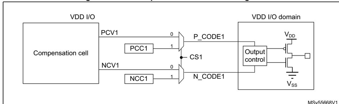
To reduce the power consumption, it is recommended to copy the code from SYSCFG_CCVR to SYSCFG_CCCR. After the result is ready, set the CS bit and disable the compensation cell.
Table 125. Effect of low-power modes on I/O compensation
| Mode | Description |
|---|---|
| Sleep | Compensation value applied on I/Os. |
| Stop | Compensation cell controlled by the EN bit of the SYSCFG_CCCSR register. |
| Standby | Default compensation value applied on I/Os. Compensation cell disabled. |
14.2.2 SYSCFG TrustZone ® security and privilege
SYSCFG TrustZone security
When the TrustZone security is activated, the SYSCFG is able to secure registers from being modified by nonsecure access.
The TrustZone security is activated by the TZEN user option bit in the FLASH_OPTR register.
Nonsecure read/write access to a secured register is RAZ/WI and generates an illegal access event. An illegal access interrupt is generated if the SYSCFG illegal access event is enabled in the GTZC1_TZIC.
As soon as at least one function is configured to be secured, the SYSCFG reset and clock control bits in the RCC are also secured.
Privileged/unprivileged mode
The SYSCFG registers can be read and written by privileged or unprivileged access except the SYSCFG registers for CPU configuration: SYSCFG_CSLCKR, SYSCFG_FPUIMR and SYSCFG_CNSLCKR registers, and the FPUSEC bit in the SYSCFG_SECCFGR register.
An unprivileged access to a privileged register is RAZ/WI.
The table below shows the register security overview.
Table 126. TrustZone security and privilege register access
| SYSCFG register name | Read/write access | Privileged /unprivileged access | |
|---|---|---|---|
| TrustZone configuration (1) | TZEN = 1 | TZEN = 0 | Not applicable |
| SYSCFG_SECCFGR | Read: no restriction Write: secure access only Nonsecure write is WI and generates an illegal access event. | RAZ/WI | Read: no restriction FPUSEC privileged write only Other bits write: no restriction |
| SYSCFG_CSLCKR | Read/Write: secure access only Nonsecure access is RAZ/WI and generates an illegal access event. | RAZ/WI | Privileged only Unprivileged: RAZ/WI |
Table 126. TrustZone security and privilege register access (continued)
| SYSCFG register name | Read/write access | Privileged /unprivileged access | |
|---|---|---|---|
| TrustZone configuration (1) | TZEN = 1 | TZEN = 0 | Not applicable |
| SYSCFG_FPUIMR | – If FPUSEC = 1: Read/Write: secure access only Nonsecure access is RAZ/WI and generates an illegal access event. – If FPUSEC = 0: Read/Write, no restriction | No restriction | Privileged only Unprivileged: RAZ/WI |
| SYSCFG_CNSLCKR | Read/write: no restriction | No restriction | Privileged only Unprivileged: RAZ/WI |
| SYSCFG_CFGR1 | Read/Write: secure access only for secure bits depending on peripheral security bits in the GTZC1_TZSC Nonsecure access only for nonsecure bits, otherwise RAZ/WI | No restriction | No restriction |
| SYSCFG_CFGR2 | – If CLASSBSEC = 1: Read/Write: secure access only Nonsecure access is RAZ/WI and generates an illegal access event. – If CLASSBSEC = 0: Read/Write, no restriction | No restriction | No restriction |
| SYSCFG_MESR | – If SYSCFGSEC = 1: Read/Write: secure access only Nonsecure access is RAZ/WI and generates an illegal access event. – If SYSCFGSEC = 0: Read/Write, no restriction | No restriction | No restriction |
| SYSCFG_CCCSR SYSCFG_CCVR SYSCFG_CCCR | – If SYSCFGSEC = 1: Read/Write: secure access only Nonsecure access is RAZ/WI and generates an illegal access event – If SYSCFGSEC = 0:Read/Write, no restriction | No restriction | No restriction |
1. TrustZone security is activated by the TZEN user option bit in the FLASH_OPTR register.
14.3 SYSCFG registers
14.3.1 SYSCFG secure configuration register (SYSCFG_SECCFGR)
Address offset: 0x000
Reset value: 0x0000 0000
When the system is secure (TZEN = 1), this register provides write access security and can be written only when the access is secure. It can be globally write-protected, or each bit of this register can be individually write-protected. A nonsecure write access is WI and generates an illegal access event. There are no read restrictions.
When the system is not secure (TZEN = 0), this register is RAZ/WI.
This register can be read and written by privileged and unprivileged access, except for FPUSEC that can be written only with privileged access.
| 31 | 30 | 29 | 28 | 27 | 26 | 25 | 24 | 23 | 22 | 21 | 20 | 19 | 18 | 17 | 16 |
|---|---|---|---|---|---|---|---|---|---|---|---|---|---|---|---|
| Res. | Res. | Res. | Res. | Res. | Res. | Res. | Res. | Res. | Res. | Res. | Res. | Res. | Res. | Res. | Res. |
| 15 | 14 | 13 | 12 | 11 | 10 | 9 | 8 | 7 | 6 | 5 | 4 | 3 | 2 | 1 | 0 |
| Res. | Res. | Res. | Res. | Res. | Res. | Res. | Res. | Res. | Res. | Res. | Res. | FPUSEC | Res. | CLASSBSEC | SYSCFGSEC |
| rw | rw | rw |
Bits 31:4 Reserved, must be kept at reset value.
Bit 3 FPUSEC : FPU security
0: SYSCFG_FPUIMR register can be read and written by secure and nonsecure access.
1: SYSCFG_FPUIMR register can be read and written by secure access only.
Bit 2 Reserved, must be kept at reset value.
Bit 1 CLASSBSEC : Class B security
0: SYSCFG_CFGR2 register can be read and written by secure and nonsecure access.
1: SYSCFG_CFGR2 register can be read and written by secure access only.
Bit 0 SYSCFGSEC : SYSCFG clock control, memory erase status and compensation cell registers security
0: SYSCFG configuration clock in RCC registers, SYSCFG_MESR and SYSCFG_CCCSR, SYSCFG_CCVR and SYSCFG_CCCR can be read and written by secure and nonsecure access.
1: SYSCFG configuration clock in RCC registers, SYSCFG_MESR and SYSCFG_CCCSR, SYSCFG_CCVR and SYSCFG_CCCR can be read and written by secure access only.
14.3.2 SYSCFG configuration register 1 (SYSCFG_CFGR1)
Address offset: 0x004
Reset value: 0x0000 0000
When the system is secure (TZEN = 1), this register can be a mix of secure and nonsecure bits depending on the security configuration bit in the GTZC1_TZSC peripheral and the
GPIO port pin security configuration in the GPIO peripheral. A nonsecure read/write access on secured bits is RAZ/WI.
When the system is not secure (TZEN = 0), there is no access restriction.
This register can be read and written by privileged and unprivileged access.
| 31 | 30 | 29 | 28 | 27 | 26 | 25 | 24 | 23 | 22 | 21 | 20 | 19 | 18 | 17 | 16 |
|---|---|---|---|---|---|---|---|---|---|---|---|---|---|---|---|
| RF_EXTPABYP2_INV | RF_EXTPABYP1_INV | Res. | Res. | Res. | Res. | Res. | Res. | Res. | Res. | Res. | Res. | PB3_FMP | PA15_FMP | PA7_FMP | PA6_FMP |
| rw | rw | rw | rw | rw | rw | ||||||||||
| 15 | 14 | 13 | 12 | 11 | 10 | 9 | 8 | 7 | 6 | 5 | 4 | 3 | 2 | 1 | 0 |
| Res. | Res. | Res. | Res. | Res. | Res. | ANASWDD | BOOSTEN | Res. | Res. | Res. | Res. | Res. | Res. | Res. | Res. |
| rw | rw |
Bit 31 RF_EXTPABYP2_INV : signal RF_EXTPABYP2 inversion selection.
This bit can be read and written only with secure access if GTZC1_TZSC RADIOSEC is secure. This bit selects the inversion or not of the RF_EXTPABYP2 signal.
0: RF_EXTPABYP2 not inverted.
1: RF_EXTPABYP2 inverted.
Bit 30 RF_EXTPABYP1_INV : signal RF_EXTPABYP1 inversion selection.
This bit can be read and written only with secure access if GTZC1_TZSC RADIOSEC is secure. This bit selects the inversion or not of the RF_EXTPABYP1 signal.
0: RF_EXTPABYP1 not inverted.
1: RF_EXTPABYP1 inverted.
Bits 29:20 Reserved, must be kept at reset value.
Bit 19 PB3_FMP : Fast mode plus drive capability activation on PB3
This bit can be read and written only with secure access if PB3 is secure in GPIOB. This bit enables the fast mode plus drive mode for PB3 when PB3 is not used by I2C peripheral. This can be used to drive a LED for instance.
0: PB3 pin operates in standard mode when not used by I2C peripheral
1: Fast mode plus mode is enabled on PAB3 pin and the GPIO speed control is bypassed.
Bit 18 PA15_FMP : Fast mode plus drive capability activation on PA15
This bit can be read and written only with secure access if PA15 is secure in GPIOA. This bit enables the fast mode plus drive mode for PA15 when PA15 is not used by I2C peripheral. This can be used to drive a LED for instance.
0: PA15 pin operates in standard mode when not used by I2C peripheral
1: fFst mode plus mode is enabled on PA15 pin and the GPIO speed control is bypassed.
Bit 17 PA7_FMP : Fast mode plus drive capability activation on PA7
This bit can be read and written only with secure access if PA7 is secure in GPIOA. This bit enables the fast mode plus drive mode for PA7 when PA7 is not used by I2C peripheral. This can be used to drive a LED for instance.
0: PA7 pin operates in standard mode when not used by I2C peripheral
1: Fast mode plus mode is enabled on PA7 pin and the GPIO speed control is bypassed.
Bit 16 PA6_FMP : Fast mode plus drive capability activation on PA6
This bit can be read and written only with secure access if PA6 is secure in GPIOA. This bit enables the fast mode plus drive mode for PA6 when PA6 is not used by I2C peripheral. This can be used to drive a LED for instance.
0: PA6 pin operates in standard mode when not used by I2C peripheral
1: Fast mode plus mode is enabled on PA6 pin and the GPIO speed control is bypassed.
Bits 15:10 Reserved, must be kept at reset value.
Bit 9 ANASWVDD : GPIO analog switch control voltage selection
Access can be protected by GTZC1_TZSC ADC4SEC.
0: I/O analog switches are supplied by \( V_{DDA} \) or booster when booster is ON.
1: I/O analog switches are supplied by \( V_{DD} \) .
Note: Refer to Table 127 for settings.
Bit 8 BOOSTEN : I/O analog switch voltage booster enable
Access can be protected by GTZC1_TZSC ADC4SEC.
0: I/O analog switches are supplied by \( V_{DDA} \) voltage.
1: I/O analog switches are supplied by a dedicated voltage booster (supplied by \( V_{DD} \) ).
Note: Refer to Table 127 for settings.
Bits 7:0 Reserved, must be kept at reset value.
Table 127 describes when the BOOSTEN and the ANASWVDD must be set or cleared, depending on the voltage settings.
Table 127. BOOSTEN and ANASWVDD set/cleared
| \( V_{DD} \) | \( V_{DDA} \) | BOOSTEN | ANASWVDD |
|---|---|---|---|
| - | \( > 2.4\text{ V} \) | 0 | |
| \( > 2.4\text{ V} \) | \( \leq 2.4\text{ V} \) | 0 | 1 |
| \( \leq 2.4\text{ V} \) | 1 | 0 |
14.3.3 SYSCFG FPU interrupt mask register (SYSCFG_FPUIMR)
Address offset: 0x008
Reset value: 0x0000 001F
This register can be read and written by privileged access only. Unprivileged access is RAZ/WI.
When the system is secure (TZEN = 1), this register can be protected against nonsecure access by setting the FPUSEC bit in the SYSCFG_SECCFGR register: nonsecure read/write access is RAZ/WI and generates an illegal access event.
When the system is not secure (TZEN = 0), there is no access restriction.
This register can be read and written by privileged access only. Unprivileged access is RAZ/WI.
| 31 | 30 | 29 | 28 | 27 | 26 | 25 | 24 | 23 | 22 | 21 | 20 | 19 | 18 | 17 | 16 |
|---|---|---|---|---|---|---|---|---|---|---|---|---|---|---|---|
| Res. | Res. | Res. | Res. | Res. | Res. | Res. | Res. | Res. | Res. | Res. | Res. | Res. | Res. | Res. | Res. |
| 15 | 14 | 13 | 12 | 11 | 10 | 9 | 8 | 7 | 6 | 5 | 4 | 3 | 2 | 1 | 0 |
| Res. | Res. | Res. | Res. | Res. | Res. | Res. | Res. | Res. | Res. | FPU_IE[5:0] | |||||
| rw | rw | rw | rw | rw | rw | ||||||||||
Bits 31:6 Reserved, must be kept at reset value.
Bits 5:0 FPU_IE[5:0] : Floating point unit interrupts enable bits
FPU_IE[5]: Inexact interrupt enable (interrupt disable at reset)
FPU_IE[4]: Input abnormal interrupt enable
FPU_IE[3]: Overflow interrupt enable
FPU_IE[2]: Underflow interrupt enable
FPU_IE[1]: Divide-by-zero interrupt enable
FPU_IE[0]: Invalid operation Interrupt enable
14.3.4 SYSCFG CPU nonsecure lock register (SYSCFG_CNSLCKR)
Address offset: 0x00C
Reset value: 0x0000 0000
This register is used to lock the configuration of MPU and VTOR registers. This register can be read and written by privileged access only. Unprivileged access is RAZ/WI.
| 31 | 30 | 29 | 28 | 27 | 26 | 25 | 24 | 23 | 22 | 21 | 20 | 19 | 18 | 17 | 16 |
|---|---|---|---|---|---|---|---|---|---|---|---|---|---|---|---|
| Res. | Res. | Res. | Res. | Res. | Res. | Res. | Res. | Res. | Res. | Res. | Res. | Res. | Res. | Res. | Res. |
| 15 | 14 | 13 | 12 | 11 | 10 | 9 | 8 | 7 | 6 | 5 | 4 | 3 | 2 | 1 | 0 |
| Res. | Res. | Res. | Res. | Res. | Res. | Res. | Res. | Res. | Res. | Res. | Res. | Res. | Res. | LOCKNSMPU | LOCKNSVTOR |
| rs | rs |
Bits 31:2 Reserved, must be kept at reset value.
Bit 1 LOCKNSMPU : MPU registers lock
This bit is set by software and cleared only by a system reset. When set, this bit disables write access to nonsecure MPU_CTRL, MPU_RNR and MPU_RBAR registers.
0: Nonsecure MPU registers write enabled
1: Nonsecure MPU registers write disabled
Bit 0 LOCKNSVTOR : VTOR register lock
This bit is set by software and cleared only by a system reset.
0: VTOR register write enabled
1: VTOR register write disabled
14.3.5 SYSCFG CPU secure lock register (SYSCFG_CSLOCKR)
Address offset: 0x010
Reset value: 0x0000 0000
This register is used to lock the configuration of PRIS and BFHFNMINS bits in the AIRCR register, SAU, secure MPU and VTOR_S registers.
When the system is secure (TZEN = 1), this register can be written only when the access is secure. Nonsecure read/write access is RAZ/WI and generates an illegal access event.
When the system is not secure (TZEN = 0), this register is RAZ/WI
This register can be read and written by privileged access only. Unprivileged access is RAZ/WI.
| 31 | 30 | 29 | 28 | 27 | 26 | 25 | 24 | 23 | 22 | 21 | 20 | 19 | 18 | 17 | 16 |
|---|---|---|---|---|---|---|---|---|---|---|---|---|---|---|---|
| Res. | Res. | Res. | Res. | Res. | Res. | Res. | Res. | Res. | Res. | Res. | Res. | Res. | Res. | Res. | Res. |
| 15 | 14 | 13 | 12 | 11 | 10 | 9 | 8 | 7 | 6 | 5 | 4 | 3 | 2 | 1 | 0 |
| Res. | Res. | Res. | Res. | Res. | Res. | Res. | Res. | Res. | Res. | Res. | Res. | Res. | LOCKSAU | LOCKNSMPU | LOCKNSVTOR |
| rs | rs | rs |
Bits 31:3 Reserved, must be kept at reset value.
Bit 2 LOCKSAU : SAU registers lock
This bit is set by software and cleared only by a system reset. When set, this bit disables write access to SAU_CTRL, SAU_RNR, SAU_RBAR and SAU_RLAR registers.
0: SAU registers write enabled
1: SAU registers write disabled
Bit 1 LOCKSMPU : Secure MPU registers lock
This bit is set by software and cleared only by a system reset. When set, this bit disables write access to secure MPU_CTRL, MPU_RNR and MPU_RBAR registers.
0: Secure MPU registers writes enabled
1: Secure MPU registers writes disabled
Bit 0 LOCKSVT AIRCR : VTOR_S register and AIRCR register bits lock
This bit is set by software and cleared only by a system reset. When set, this bit disables write access to the VTOR_S register, and the PRIS and the BFHFNMINS bits in the AIRCR register.
0: VTOR_S register PRIS and BFHFNMINS bits in the AIRCR register write enabled
1: VTOR_S register PRIS and BFHFNMINS bits in the AIRCR register write disabled
14.3.6 SYSCFG configuration register 2 (SYSCFG_CFGR2)
Address offset: 0x014
Reset value: 0x0000 0000
When the system is secure (TZEN = 1), this register can be protected against nonsecure access by setting the CLASSBSEC bit in the SYSCFG_SECCFGR register. When the CLASSBSEC bit is set, only secure access is allowed: nonsecure read/write access is RAZ/WI and generates an illegal access event.
When the system is not secure (TZEN = 0), there is no access restriction.
This register can be read and written by privileged and unprivileged access.
| 31 | 30 | 29 | 28 | 27 | 26 | 25 | 24 | 23 | 22 | 21 | 20 | 19 | 18 | 17 | 16 |
|---|---|---|---|---|---|---|---|---|---|---|---|---|---|---|---|
| Res. | Res. | Res. | Res. | Res. | Res. | Res. | Res. | Res. | Res. | Res. | Res. | Res. | Res. | Res. | Res. |
| 15 | 14 | 13 | 12 | 11 | 10 | 9 | 8 | 7 | 6 | 5 | 4 | 3 | 2 | 1 | 0 |
| Res. | Res. | Res. | Res. | Res. | Res. | Res. | Res. | Res. | Res. | Res. | Res. | ECCL rs | PVDL rs | SPL rs | CLL rs |
Bits 31:4 Reserved, must be kept at reset value.
Bit 3 ECCL : ECC lock
This bit is set by software and cleared only by a system reset. It can be used to enable and lock the flash ECC double error signal connection to TIM16 and TIM17 break input.
0: ECC double error disconnected from TIM16 and TIM17 break input
1: ECC double error connected to TIM16 and TIM17 break input
Bit 2 PVDL : PVD lock enable bit
This bit is set by software and cleared only by a system reset. It can be used to enable and lock the PVD connection to TIM16 and TIM17 break input, as well as the PVDE and PVDLS[2:0] in the PWR register.
0: PVD interrupt disconnected from TIM16 and TIM17 break input. PVDE and PVDLS[2:0] bits can be programmed by the application.
1: PVD interrupt connected to TIM16 and TIM17 break input. PVDE and PVDLS[2:0] bits are read only.
Bit 1 SPL : SRAM2 parity lock bit
This bit is set by software and cleared only by a system reset. It can be used to enable and lock the SRAM2 parity error signal connection to TIM16 and TIM17 break inputs.
0: SRAM2 parity error disconnected from TIM16 and TIM17 break inputs
1: SRAM2 parity error connected to TIM16 and TIM17 break inputs
Bit 0 CLL : Cortex-M33 LOCKUP (hardfault) output enable
This bit is set by software and cleared only by a system reset. It can be used to enable and lock the connection of Cortex-M33 LOCKUP (hardfault) output to TIM16 and TIM17 break input.
0: Cortex-M33 LOCKUP output disconnected from TIM16 to TIM17 break inputs
1: Cortex-M33 LOCKUP output connected to TIM16 and TIM17 break inputs
14.3.7 SYSCFG memory erase status register (SYSCFG_MESR)
Address offset: 0x018
Power-on reset value: 0x0000 0000
System reset value: 0x0000 000X (bit MCLR not affected by system reset)
When the system is secure (TZEN = 1), this register can be protected against nonsecure access by setting the SYSCFGSEC bit in the SYSCFG_SECCFGR register. When the SYSCFGSEC bit is set, only secure access is allowed: nonsecure read/write access is RAZ/WI and generates an illegal access event.
When the system is not secure (TZEN = 0), there is no access restriction.
This register can be read and written by privileged and unprivileged access.
| 31 | 30 | 29 | 28 | 27 | 26 | 25 | 24 | 23 | 22 | 21 | 20 | 19 | 18 | 17 | 16 |
|---|---|---|---|---|---|---|---|---|---|---|---|---|---|---|---|
| Res. | Res. | Res. | Res. | Res. | Res. | Res. | Res. | Res. | Res. | Res. | Res. | Res. | Res. | Res. | IPMEE |
| rc_w1 | |||||||||||||||
| 15 | 14 | 13 | 12 | 11 | 10 | 9 | 8 | 7 | 6 | 5 | 4 | 3 | 2 | 1 | 0 |
| Res. | Res. | Res. | Res. | Res. | Res. | Res. | Res. | Res. | Res. | Res. | Res. | Res. | Res. | Res. | MCLR |
| rc_w1 |
Bits 31:17 Reserved, must be kept at reset value.
Bit 16 IPMEE : ICACHE and PKA SRAM erase status
This bit is set by hardware when ICACHE and PKA SRAM erase is completed after potential tamper detection (refer to Section 34: Tamper and backup registers (TAMP) for more details).
This bit is cleared by software by writing 1 to it.
0: ICACHE and PKA SRAM erase ongoing if not yet cleared by software
1: ICACHE and PKA SRAM erase done
Bits 15:1 Reserved, must be kept at reset value.
Bit 0 MCLR : Device memories erase status
This bit is set by hardware when SRAM2, ICACHE, and PKA SRAM erase is completed after power-on reset or tamper detection (refer to Section 34: Tamper and backup registers (TAMP) for more details). This bit is not cleared by system reset. It is cleared by software by writing 1 to it.
0: Memory erase ongoing if not yet cleared by software
1: Memory erase done
14.3.8 SYSCFG compensation cell control/status register (SYSCFG_CCCSR)
Address offset: 0x01C
Reset value: 0x0000 0002
When the system is secure (TZEN = 1), this register can be protected against nonsecure access by setting the SYSCFGSEC bit in the SYSCFG_SECCFGR register. When the SYSCFGSEC bit is set, only secure access is allowed: nonsecure read/write access is RAZ/WI and generates an illegal access event.
When the system is not secure (TZEN = 0), there is no access restriction.
This register can be read and written by privileged and unprivileged access.
| 31 | 30 | 29 | 28 | 27 | 26 | 25 | 24 | 23 | 22 | 21 | 20 | 19 | 18 | 17 | 16 |
|---|---|---|---|---|---|---|---|---|---|---|---|---|---|---|---|
| Res. | Res. | Res. | Res. | Res. | Res. | Res. | Res. | Res. | Res. | Res. | Res. | Res. | Res. | Res. | Res. |
| 15 | 14 | 13 | 12 | 11 | 10 | 9 | 8 | 7 | 6 | 5 | 4 | 3 | 2 | 1 | 0 |
| Res. | Res. | Res. | Res. | Res. | Res. | Res. | RDY1 | Res. | Res. | Res. | Res. | Res. | Res. | CS1 | EN1 |
| r | rw | rw | |||||||||||||
Bits 31:9 Reserved, must be kept at reset value.
Bit 8 RDY1 : V DD I/Os compensation cell ready flag
This bit provides the compensation cell status of the I/Os supplied by \( V_{DD} \) .
- 0: V DD I/Os compensation cell not ready
- 1: V DD I/Os compensation cell ready
Note: The HSI16 clock is required for the compensation cell to work properly. The compensation cell ready bit (RDY1) is not set if the HSI16 clock is not enabled (HSION).
Bits 7:2 Reserved, must be kept at reset value.
Bit 1 CS1 : V DD I/Os code selection
This bit selects the code to be applied for the compensation cell of the I/Os supplied by \( V_{DD} \) .
- 0: V DD I/Os code from the cell (available in the SYSCFG_CCVR register)
- 1: V DD I/Os code from the SYSCFG compensation cell code register (SYSCFG_CCCR)
Bit 0 EN1 : V DD I/Os compensation cell enable
This bit enables the compensation cell of the I/Os supplied by \( V_{DD} \) .
- 0: V DD I/Os compensation cell disabled
- 1: V DD I/Os compensation cell enabled
14.3.9 SYSCFG compensation cell value register (SYSCFG_CCVR)
Address offset: 0x020
Reset value: 0x0000 0000
When the system is secure (TZEN = 1), this register can be protected against nonsecure access by setting the SYSCFGSEC bit in the SYSCFG_SECCFGR register. When the SYSCFGSEC bit is set, only secure access is allowed: nonsecure read/write access is RAZ/WI and generates an illegal access event.
When the system is not secure (TZEN = 0), there is no access restriction.
This register can be read and written by privileged and unprivileged access.
| 31 | 30 | 29 | 28 | 27 | 26 | 25 | 24 | 23 | 22 | 21 | 20 | 19 | 18 | 17 | 16 |
|---|---|---|---|---|---|---|---|---|---|---|---|---|---|---|---|
| Res. | Res. | Res. | Res. | Res. | Res. | Res. | Res. | Res. | Res. | Res. | Res. | Res. | Res. | Res. | Res. |
| 15 | 14 | 13 | 12 | 11 | 10 | 9 | 8 | 7 | 6 | 5 | 4 | 3 | 2 | 1 | 0 |
| Res. | Res. | Res. | Res. | Res. | Res. | Res. | Res. | PCV1[3:0] | NCV1[3:0] | ||||||
| r | r | r | r | r | r | r | r | ||||||||
Bits 31:8 Reserved, must be kept at reset value.
Bits 7:4 PCV1[3:0] : PMOS compensation value of the I/Os supplied by V DD
This value is provided by the cell and can be used by the CPU to compute an I/Os compensation cell code for PMOS transistors. This code is applied to the I/Os compensation cell when the CS1 bit of the SYSCFG_CCCSR register is cleared.
Bits 3:0 NCV1[3:0] : NMOS compensation value of the I/Os supplied by V DD
This value is provided by the cell and can be used by the CPU to compute an I/Os compensation cell code for NMOS transistors. This code is applied to the I/Os compensation cell when the CS1 bit of the SYSCFG_CCCSR is cleared.
14.3.10 SYSCFG compensation cell code register (SYSCFG_CCCR)
Address offset: 0x024
Reset value: 0x0000 0078
When the system is secure (TZEN = 1), this register can be protected against nonsecure access by setting the SYSCFGSEC bit in the SYSCFG_SECCFGR register. When the SYSCFGSEC bit is set, only secure access is allowed: nonsecure read/write access is RAZ/WI and generates an illegal access event.
When the system is not secure (TZEN = 0), there is no access restriction.
This register can be read and written by privileged and unprivileged access.
| 31 | 30 | 29 | 28 | 27 | 26 | 25 | 24 | 23 | 22 | 21 | 20 | 19 | 18 | 17 | 16 |
|---|---|---|---|---|---|---|---|---|---|---|---|---|---|---|---|
| Res. | Res. | Res. | Res. | Res. | Res. | Res. | Res. | Res. | Res. | Res. | Res. | Res. | Res. | Res. | Res. |
| 15 | 14 | 13 | 12 | 11 | 10 | 9 | 8 | 7 | 6 | 5 | 4 | 3 | 2 | 1 | 0 |
| Res. | Res. | Res. | Res. | Res. | Res. | Res. | Res. | PCC1[3:0] | NCC1[3:0] | ||||||
| rw | rw | rw | rw | rw | rw | rw | rw | ||||||||
Bits 31:8 Reserved, must be kept at reset value.
Bits 7:4 PCC1[3:0] : PMOS compensation code of the I/Os supplied by \( V_{DD} \)
These bits are written by software to define an I/Os compensation cell code for PMOS transistors. This code is applied to the I/Os compensation cell when the CS1 bit of the SYSCFG_CCCSR is set.
Bits 3:0 NCC1[3:0] : NMOS compensation code of the I/Os supplied by \( V_{DD} \)
These bits are written by software to define an I/Os compensation cell code for NMOS transistors. This code is applied to the I/Os compensation cell when the CS1 bit of the SYSCFG_CCCSR is set.
14.3.11 SYSCFG flash abort interrupt enable register (SYSCFG_FAIER)
Address offset: 0x110
Reset value: 0x0000 0000
This register can be read and written by privileged access only. An unprivileged read/write access is RAZ/WI.
| 31 | 30 | 29 | 28 | 27 | 26 | 25 | 24 | 23 | 22 | 21 | 20 | 19 | 18 | 17 | 16 |
|---|---|---|---|---|---|---|---|---|---|---|---|---|---|---|---|
| Res. | Res. | Res. | Res. | Res. | Res. | Res. | USB | Res. | Res. | Res. | WKUP_S | WKUP | RADIO | Res. | SPI3 |
| rw | rw | rw | rw | rw | |||||||||||
| 15 | 14 | 13 | 12 | 11 | 10 | 9 | 8 | 7 | 6 | 5 | 4 | 3 | 2 | 1 | 0 |
| SAI1 | I2C3_EV | LPUART1 | Res. | USART1 | Res. | I2C1_EV | LPDMA_CH3 | LPDMA_CH2 | LPDMA_CH1 | LPDMA_CH0 | EXTI5 | EXTI4 | EXTI3 | EXTI2 | PVD |
| rw | rw | rw | rw | rw | rw | rw | rw | rw | rw | rw | rw | rw | rw |
Bits 31:25 Reserved, must be kept at reset value.
Bit 24 USB : enable USB interrupt to abort flash operation.
Access can be secured by GTZC1_TZSC USBSEC. When secure, nonsecure read/write access is RAZ/WI. It does not generate an illegal access interrupt.
0: USB interrupt abort flash operation disabled
1: USB interrupt abort flash operation enabled
Note: This bit is reserved on STM32WBA23xx devices.
Bits 23:21 Reserved, must be kept at reset value.
Bit 20 WKUP_S : enable PWR WKUP secure interrupt to abort flash operation.
Access is always secure, nonsecure read/write access is RAZ/WI. It does not generate an illegal access interrupt.
0: PWR WKUP secure interrupt abort flash operation disabled
1: PWR WKUP secure interrupt abort flash operation enabled
Bit 19 WKUP : enable PWR WKUP interrupt to abort flash operation.
This bit can be access read/write secure and nonsecure.
0: PWR WKUP interrupt abort flash operation disabled
1: PWR WKUP interrupt abort flash operation enabled
Bit 18 RADIO : enable RADIO interrupt to abort flash operation.
Access can be secured by GTZC1_TZSC RADIOSEC. When secure, nonsecure read/write access is RAZ/WI. It does not generate an illegal access interrupt.
0: RADIO interrupt abort flash operation disabled
1: RADIO interrupt abort flash operation enabled
Bit 17 Reserved, must be kept at reset value.
Bit 16 SPI3 : enable SPI3 interrupt to abort flash operation.
Access can be secured by GTZC1_TZSC SPI3SEC. When secure, nonsecure read/write access is RAZ/WI. It does not generate an illegal access interrupt.
0: SPI3 interrupt abort flash operation disabled
1: SPI3 interrupt abort flash operation enabled
Bit 15 SAI1 : enable SAI1 interrupt to abort flash operation.
Access can be secured by GTZC1_TZSC SAI1SEC. When secure, nonsecure read/write access is RAZ/WI. It does not generate an illegal access interrupt.
0: SAI1 interrupt abort flash operation disabled
1: SAI1 interrupt abort flash operation enabled
Bit 14 I2C3_EV : enable I2C3_EV interrupt to abort flash operation.
Access can be secured by GTZC1_TZSC I2C3SEC. When secure, nonsecure read/write access is RAZ/WI. It does not generate an illegal access interrupt.
0: I2C3_EV interrupt abort flash operation disabled
1: I2C3_EV interrupt abort flash operation enabled
Bit 13 LPUART1 : enable LPUART1 interrupt to abort flash operation.
Access can be secured by GTZC1_TZSC LPUART1SEC. When secure, nonsecure read/write access is RAZ/WI. It does not generate an illegal access interrupt.
0: LPUART1 interrupt abort flash operation disabled
1: LPUART1 interrupt abort flash operation enabled
Bit 12 Reserved, must be kept at reset value.
Bit 11 USART1 : enable USART1 interrupt to abort flash operation.
Access can be secured by GTZC1_TZSC USART1SEC. When secure, nonsecure read/write access is RAZ/WI. It does not generate an illegal access interrupt.
0: USART1 interrupt abort flash operation disabled
1: USART1 interrupt abort flash operation enabled
Bit 10 Reserved, must be kept at reset value.
Bit 9 I2C1_EV : enable I2C1_EV interrupt to abort flash operation.
Access can be secured by GTZC1_TZSC I2C1SEC. When secure, nonsecure read/write access is RAZ/WI. It does not generate an illegal access interrupt.
0: I2C1_EV interrupt abort flash operation disabled
1: I2C1_EV interrupt abort flash operation enabled
Bit 8 LPDMA_CH3 : enable LPDMA_CH3 interrupt to abort flash operation.
Access can be secured by LPDMA SEC3. When secure, nonsecure read/write access is RAZ/WI. It does not generate an illegal access interrupt.
0: LPDMA_CH3 interrupt abort flash operation disabled
1: LPDMA_CH3 interrupt abort flash operation enabled
Bit 7 LPDMA_CH2 : enable LPDMA_CH2 interrupt to abort flash operation.
Access can be secured by LPDMA SEC2. When secure, nonsecure read/write access is RAZ/WI. It does not generate an illegal access interrupt.
0: LPDMA_CH2 interrupt abort flash operation disabled
1: LPDMA_CH2 interrupt abort flash operation enabled
Bit 6 LPDMA_CH1 : enable LPDMA_CH1 interrupt to abort flash operation.
Access can be secured by LPDMA SEC1. When secure, nonsecure read/write access is RAZ/WI. It does not generate an illegal access interrupt.
0: LPDMA_CH1 interrupt abort flash operation disabled
1: LPDMA_CH1 interrupt abort flash operation enabled
Bit 5 LPDMA_CH0 : enable LPDMA_CH0 interrupt to abort flash operation.
Access can be secured by LPDMA SEC0. When secure, nonsecure read/write access is RAZ/WI. It does not generate an illegal access interrupt.
0: LPDMA_CH0 interrupt abort flash operation disabled
1: LPDMA_CH0 interrupt abort flash operation enabled
Bit 4 EXTI5 : enable EXTI5 interrupt to abort flash operation.
Access can be secured by EXTI SEC5. When secure, nonsecure read/write access is RAZ/WI. It does not generate an illegal access interrupt.
0: EXTI5 interrupt abort flash operation disabled
1: EXTI5 interrupt abort flash operation enabled
Bit 3 EXTI4 : enable EXTI4 interrupt to abort flash operation.
Access can be secured by EXTI SEC4. When secure, nonsecure read/write access is RAZ/WI. It does not generate an illegal access interrupt.
0: EXTI4 interrupt abort flash operation disabled
1: EXTI4 interrupt abort flash operation enabled
Bit 2 EXTI3 : enable EXTI3 interrupt to abort flash operation.
Access can be secured by EXTI SEC3. When secure, nonsecure read/write access is RAZ/WI. It does not generate an illegal access interrupt.
0: EXTI3 interrupt abort flash operation disabled
1: EXTI3 interrupt abort flash operation enabled
Bit 1 EXTI2 : enable EXTI2 interrupt to abort flash operation.
Access can be secured by EXTI SEC2. When secure, nonsecure read/write access is RAZ/WI. It does not generate an illegal access interrupt.
0: EXTI2 interrupt abort flash operation disabled
1: EXTI2 interrupt abort flash operation enabled
Bit 0 PVD : enable EXTI16 PVD interrupt to abort flash operation.
Access can be secured by EXTI SEC16. When secure, nonsecure read/write access is RAZ/WI. It does not generate an illegal access interrupt.
0: PVD EXTI16 interrupt abort flash operation disabled
1: PVD EXTI16 interrupt abort flash operation enabled
14.3.12 SYSCFG register map
Table 128. SYSCFG register map and reset values
| Offset | Register | 31 | 30 | 29 | 28 | 27 | 26 | 25 | 24 | 23 | 22 | 21 | 20 | 19 | 18 | 17 | 16 | 15 | 14 | 13 | 12 | 11 | 10 | 9 | 8 | 7 | 6 | 5 | 4 | 3 | 2 | 1 | 0 |
|---|---|---|---|---|---|---|---|---|---|---|---|---|---|---|---|---|---|---|---|---|---|---|---|---|---|---|---|---|---|---|---|---|---|
| 0x000 | SYSCFG_SECCFGR | Res. | Res. | Res. | Res. | Res. | Res. | Res. | Res. | Res. | Res. | Res. | Res. | Res. | Res. | Res. | Res. | Res. | Res. | Res. | Res. | Res. | Res. | Res. | Res. | Res. | Res. | Res. | Res. | Res. | Res. | Res. | Res. |
| Reset value | 0 | 0 | 0 | ||||||||||||||||||||||||||||||
| 0x004 | SYSCFG_CFGR1 | RF_EXTABYP2_INV | RF_EXTABYP1_INV | Res. | Res. | Res. | Res. | Res. | Res. | Res. | Res. | Res. | Res. | Res. | PB3_FMP | PA15_FMP | PA7_FMP | PA6_FMP | Res. | Res. | Res. | Res. | Res. | ANASWVDD | BOOSTEN | Res. | Res. | Res. | Res. | Res. | Res. | Res. | Res. |
| Reset value | 0 | 0 | 0 | 0 | 0 | 0 | 0 | 0 | |||||||||||||||||||||||||
| 0x008 | SYSCFG_FPUIMR | Res. | Res. | Res. | Res. | Res. | Res. | Res. | Res. | Res. | Res. | Res. | Res. | Res. | Res. | Res. | Res. | Res. | Res. | Res. | Res. | Res. | Res. | Res. | Res. | Res. | Res. | Res. | Res. | Res. | Res. | Res. | FPU_IE[5:0] |
| Reset value | 1 | 1 | 1 | 1 | |||||||||||||||||||||||||||||
| 0x00C | SYSCFG_CNSLCKR | Res. | Res. | Res. | Res. | Res. | Res. | Res. | Res. | Res. | Res. | Res. | Res. | Res. | Res. | Res. | Res. | Res. | Res. | Res. | Res. | Res. | Res. | Res. | Res. | Res. | Res. | Res. | Res. | Res. | Res. | LOCKNSMPU | LOCKNSVTOR |
| Reset value | 0 | 0 | |||||||||||||||||||||||||||||||
| 0x010 | SYSCFG_CSLOCKR | Res. | Res. | Res. | Res. | Res. | Res. | Res. | Res. | Res. | Res. | Res. | Res. | Res. | Res. | Res. | Res. | Res. | Res. | Res. | Res. | Res. | Res. | Res. | Res. | Res. | Res. | Res. | Res. | Res. | LOCKSAU | LOCKSMPU | |
| Reset value | 0 | 0 | |||||||||||||||||||||||||||||||
| 0x014 | SYSCFG_CFGR2 | Res. | Res. | Res. | Res. | Res. | Res. | Res. | Res. | Res. | Res. | Res. | Res. | Res. | Res. | Res. | Res. | Res. | Res. | Res. | Res. | Res. | Res. | Res. | Res. | Res. | Res. | Res. | Res. | Res. | ECCL | PVDL | |
| Reset value | 0 | 0 | |||||||||||||||||||||||||||||||
| 0x018 | SYSCFG_MESR | Res. | Res. | Res. | Res. | Res. | Res. | Res. | Res. | Res. | Res. | Res. | Res. | Res. | Res. | Res. | IPMEE | Res. | Res. | Res. | Res. | Res. | Res. | Res. | Res. | Res. | Res. | Res. | Res. | Res. | Res. | Res. | MCLR |
| Reset value | 0 | 0 | |||||||||||||||||||||||||||||||
| 0x01C | SYSCFG_CCCSR | Res. | Res. | Res. | Res. | Res. | Res. | Res. | Res. | Res. | Res. | Res. | Res. | Res. | Res. | Res. | Res. | Res. | Res. | Res. | Res. | Res. | Res. | Res. | RDY1 | Res. | Res. | Res. | Res. | Res. | Res. | CS1 | |
| Reset value | 0 | 1 | |||||||||||||||||||||||||||||||
| 0x020 | SYSCFG_CCVR | Res. | Res. | Res. | Res. | Res. | Res. | Res. | Res. | Res. | Res. | Res. | Res. | Res. | Res. | Res. | Res. | Res. | Res. | Res. | Res. | Res. | Res. | Res. | Res. | Res. | PCV1[3:0] | Res. | Res. | Res. | NCV1[3:0] | ||
| Reset value | 0 | 0 | 0 | 0 | 0 | 0 | |||||||||||||||||||||||||||
| 0x024 | SYSCFG_CCCR | Res. | Res. | Res. | Res. | Res. | Res. | Res. | Res. | Res. | Res. | Res. | Res. | Res. | Res. | Res. | Res. | Res. | Res. | Res. | Res. | Res. | Res. | Res. | Res. | Res. | PCC1[3:0] | Res. | Res. | Res. | NCC1[3:0] | ||
| Reset value | 0 | 1 | 1 | 1 | 1 | 0 | |||||||||||||||||||||||||||
| 0x110 | SYSCFG_FAICR | Res. | Res. | Res. | Res. | Res. | Res. | Res. | USB | Res. | Res. | Res. | Res. | WKUP_S | WKUP | RADIO | Res. | SPI3 | SAI1 | I2C3_EV | LPUART1 | Res. | USART1 | Res. | I2C1_EV | LPDMA_CH3 | LPDMA_CH2 | LPDMA_CH1 | LPDMA_CH0 | EXTI5 | EXTI4 | EXTI3 | |
| Reset value | 0 | 0 | 0 | 0 | 0 | 0 | 0 | 0 | 0 | 0 | 0 | 0 | 0 | 0 | 0 | 0 | 0 | ||||||||||||||||
| 0x114 to 0x3FC | Reserved | ||||||||||||||||||||||||||||||||