12. Reset and clock control (RCC)
12.1 Introduction
The reset and clock control (RCC) manages the different kinds of reset and generates all clocks for the bus and peripherals.
12.2 RCC pins and internal signals
Table 107 lists the RCC inputs and output signals connected to package pins or balls.
Table 107. RCC input/output signals connected to package pins or balls
| Signal name | Signal type | Description |
|---|---|---|
| NRST | I/O | System reset, can be used to provide reset to external devices |
| OSC32_IN | I | 32 kHz oscillator input |
| OSC32_OUT | O | 32 kHz oscillator output |
| OSC_IN | I | System oscillator input |
| OSC_OUT | O | System oscillator output |
| MCO | O | Output clock for external devices |
| LSCO | O | Low-speed output clock for external devices |
| AUDIOCLK | I | External kernel clock input for SAI1 |
12.3 RCC reset functional description
The following types of reset exist:
- • Power reset
- • System reset
- • Backup domain reset
- • Individual peripheral reset
12.3.1 Power reset
A power reset is generated when one of the following events occurs:
- • Upon brownout reset (BOR)
- • When exiting Standby modes
A BOR sets all registers to their reset values. Five BOR threshold levels can be selected through the user option bytes. The backup domain is always reset on the \( V_{BOR0} \) threshold, as is the power-on reset.
When exiting Standby mode, all registers in the core domain are set to their reset value. Registers outside the core domain (RTC, TAMP, WKUP, IWDG, and Standby modes control) are not impacted.
12.3.2 System reset
A system reset sets all registers to their reset values, except the reset flags in the RCC control/status register (RCC_CSR) and the registers in the backup domain.
A system reset is generated when one of the following events occurs:
- • A low level on the NRST pin (external reset)
- • An independent watchdog event (IWDG reset)
- • A software reset (SW reset) (see Software reset )
- • A low-power mode security reset (see Low-power mode security reset )
- • An option byte loader reset (see Option byte loader reset )
- • A brownout reset
The reset source can be identified by checking the reset flags in the RCC control/status register (RCC_CSR) .
The device internal reset sources (such as BOR and IWDG) act on the NRST pin, which is always kept low during the delay phase. The internal reset signal is output on the NRST pin. The pulse generator ensures a minimum reset pulse duration of \( t_{O(NRST)} \) for each internal reset source (refer to the product datasheet for more details). In case of an external reset, the reset pulse is generated while the NRST pin is asserted low.
In case of an internal reset, the internal pull-up \( R_{PU} \) is deactivated to save the power consumption through the pull-up resistor.
Figure 35. Simplified diagram of the reset circuit
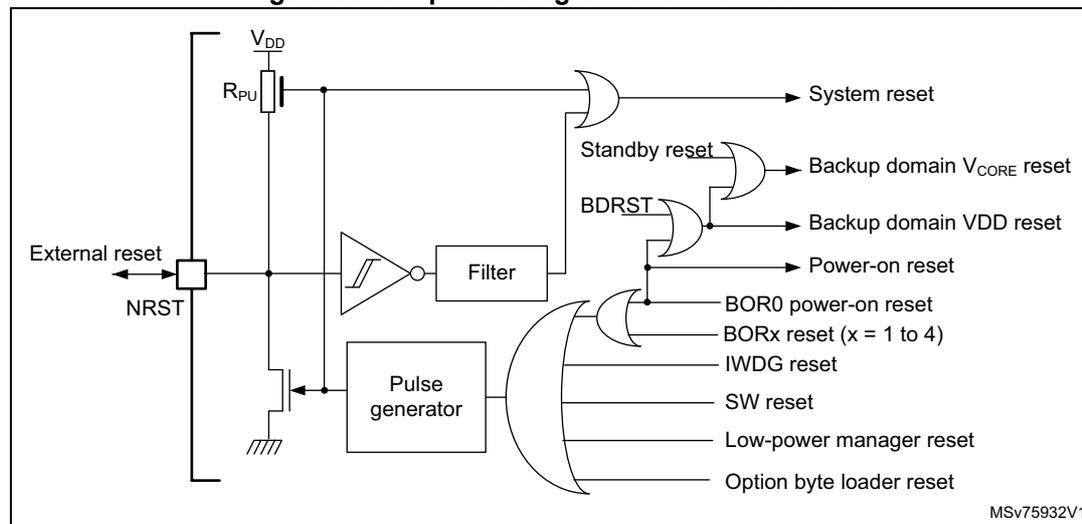
The diagram illustrates the internal reset circuitry. An external reset signal enters the NRST pin. A pull-up resistor \( R_{PU} \) connected to \( V_{DD} \) keeps the pin high when no external reset is active. The NRST signal is split into several paths:
- One path goes through an inverter and a filter to an OR gate that generates the System reset .
- Another path goes through a pulse generator to a large OR gate.
- Internal reset sources (BOR0 power-on reset, BORx reset (x = 1 to 4), IWDG reset, SW reset, Low-power manager reset, and Option byte loader reset) are also connected to this large OR gate.
- The output of the large OR gate is connected to another OR gate that generates the Power-on reset .
- The filtered NRST signal is also input to a NAND gate along with the Standby reset signal. The output of this NAND gate is connected to an OR gate that generates the Backup domain \( V_{CORE} \) reset .
- The filtered NRST signal is also input to another NAND gate along with the BDRST signal. The output of this NAND gate is connected to an OR gate that generates the Backup domain VDD reset .
Software reset
The SYSRESETREQ bit in the core application interrupt and reset control register must be set to force a software reset on the device.
Low-power mode security reset
To avoid that critical applications mistakenly enter a low-power mode, low-power mode security resets are available. If enabled in option bytes, a reset is generated in any of the following conditions:
- • Entering Stop mode: this type of reset is enabled by resetting the nRST_STOP bit in the user option bytes. In this case, whenever a Stop mode entry sequence is successfully executed, the device is reset instead of entering Stop mode.
- • Entering Standby mode: this type of reset is enabled by resetting the nRST_STDBY bit in the user option bytes. In this case, whenever a Standby mode entry sequence is successfully executed, the device is reset instead of entering Standby mode.
For further information on the user option bytes, refer to Section 7.4.1: Option bytes description .
Option byte loader reset
The option byte loader reset is generated when the OBL_LAUNCH bit is set in the FLASH_CR register. This bit is used to launch the option byte loading by software.
12.3.3 Backup domain reset
The backup domain has two specific resets.
A backup domain reset is generated when one of the following events occurs:
- • A software reset, triggered by setting the BDRST bit in the RCC backup domain control register (RCC_BDCR1)
- • A V DD supply BOR0 power-on reset
- • A V CORE supply power-on reset (only resetting the backup domain V CORE : RTC, TAMP, and backup registers).
A backup domain reset only affects the LSE oscillator, the RTC, TAMP, and backup registers, and the RCC_BDCRx registers.
12.3.4 Individual peripheral reset
Individual peripherals can be reset by software with their reset register bit in the RCC.
12.3.5 CPU reset
The CPU reset vector is selected through the boot option bytes.
12.4 RCC clocks functional description
The following clock sources can be used to drive the system clock (SYSCLK):
- • HSI16: high-speed internal 16 MHz RC oscillator clock
- • HSE32: high-speed external crystal or clock, 32 MHz
- • PLL1: clock up to 64 MHz
The HSI16 is used as the system clock source after startup from reset and is configured at 16 MHz.
The device has the following additional clock sources:
- • LSI:
- – LSI1: 32 kHz low-speed, low-power internal RC that drives the independent watchdog and, optionally, the RTC used for auto-wake-up from Stop 0, 1, 2, and Standby modes
- – LSI2: 32 kHz low-speed low drift internal RC that drives optionally the RTC or 2.4 GHz RADIO sleep timer used for auto-wake-up from Stop and Standby modes (not available on STM32WBA25/23 devices).
- • LSE: 32.768 kHz low-speed external crystal or clock that optionally drives the real-time clock (rtc_ck)
Each clock source can be switched on or off independently when it is not used, to optimize power consumption.
The frequencies for AHB1, AHB2, AHB4, and AHB5 for the PTACONV, as well as APB1, APB2, and APB7 are derived from the SYSCLK and are provided with several prescalers to configure them. The maximum frequency of these AHB and APB domains is 64 MHz.
The AHB5 frequency for the 2.4 GHz RADIO is also derived from the SYSCLK and is provided with a prescaler to configure it. The maximum frequency of this AHB5 domain is 32 MHz.
Most peripheral kernel clocks are derived from their bus clock (hclk1, hclk5, pclk1, pclk2, or pclk7). In addition, some peripherals receive an independent kernel clock. For these peripherals the kernel clock can be selected by software between several sources through the RCC_CCIPRx registers (x = 1, 2, 3):
- • RNG
- • ADC4
- • U(S)ART1
- • LPUART1
- • I2Cx (x = 1, 3)
- • SPI3
- • SAI1
- • USB
- • LPTIMx (x = 1, 2)
- • RTC and TAMP (selected in RCC_BDCR1)
- • IWDG (always LSI)
- • 2.4 GHz RADIO (always HSE32)
- • 2.4 GHz RADIO sleep timer (selected in RCC_BDCR1)
- • RCC audio synchronization
The RCC feeds the CPU system timer (SysTick) clock with the AHB clock (hclk1) divided by 8, HSI16 divided by 4, LSE, or LSI. The SysTick can work either with this clock or directly with the CPU bus clock (hclk1), configurable in the CPU SysTick control and status register.
FCLK acts as the CPU free-running clock.
Figure 36. Clock tree
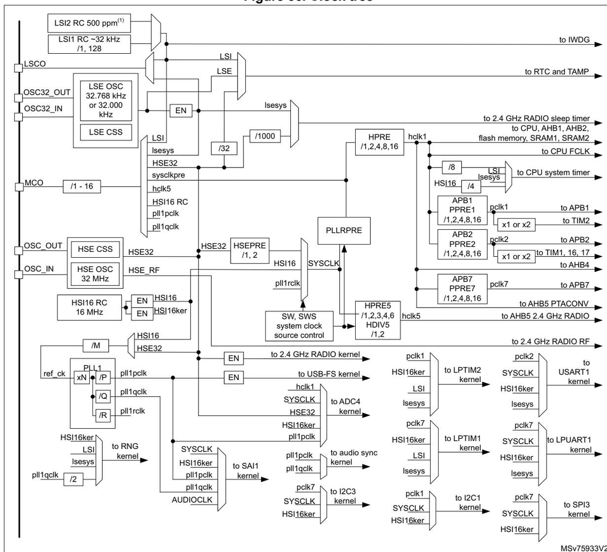
The diagram illustrates the clock tree architecture. On the left, clock sources include LSI (500 ppm and ~32 kHz), LSE (32.768 kHz or 32.000 kHz), HSE (32 MHz), HSI (16 MHz), and PLL1 (driven by HSE32, HSI16, or LSI). These are processed through various dividers (e.g., /1, /128, /32, /1000, /16, /M, /N, /P, /Q, /R) and PLLs (PLL1, PLLRPRE). The main system clock (SYSCLK) is derived from these sources. The clock is then distributed to various functional blocks:
- HPRE (High-Priority Pre-divider): Divides SYSCLK to provide hclk1 (to CPU, AHB1, AHB2, flash memory, SRAM1, SRAM2) and hclk5 (to AHB5 2.4 GHz RADIO).
- APB1 and APB2 Pre-dividers (PPRE1, PPRE2): Further divide hclk1 to provide pclk1 and pclk2 for APB1, TIM2, and TIM1.
- APB7 Pre-divider (PPRE7): Divides hclk5 to provide pclk7 for APB7 and AHB5 PTACONV.
- PLL1 outputs: Provide pll1pclk (to USB-FS kernel), pll1qclk (to ADC4 kernel), and pll1rclk (to audio sync kernel).
- HSI16ker and LSI outputs: Provide clocks for LPTIM2, LPTIM1, USART1, LPUART1, I2C1, I2C3, and SPI3 kernels.
- Other connections: LSI is connected to IWDG and RTC and TAMP. HSE32 is connected to 2.4 GHz RADIO kernel and RF. MCO is an output pin with a /1-16 divider.
12.4.1 HSE32 clock with trimming
The HSE32 32 MHz external oscillator has the advantage of producing a very accurate rate on the main clock. The HSE32 furthermore provides an on-chip trimming capability in RCC_ECSCR1. The HSE32 must be used for any 2.4 GHz RADIO transmission and reception.
The high-speed external clock signal (HSE32) can be generated from the following clock sources:
- • HSE32 external crystal
- • HSE32 external clock
The clock source must be placed as close as possible to the oscillator pins to minimize output distortion and startup stabilization time.
HSE32 is controlled from the CPU and from the 2.4 GHz RADIO.
HSE32 can be switched on and off using the HSEON bit in the RCC clock control register (RCC_CR) . HSE32 must be enabled with the HSEON bit when used for the CPU.
The HSERDY flag in the RCC clock control register (RCC_CR) indicates if the HSE32 oscillator is stable and forwarded or not for use by the CPU. At startup, the clock is not released until this bit is set by hardware. An interrupt can be generated if enabled in the RCC clock interrupt enable register (RCC_CIER) . Refer to the product datasheet for the HSE32 stabilization-ready time.
The 2.4 GHz RADIO when waking up from a sleep timer event enables HSE32 autonomously for its own purpose with STRADIOCLKON, independently of the HSEON bit. To use the 2.4 GHz RADIO outside a sleep timer event, software has to enable HSE32 with HSEON.
External crystal (HSE32 crystal)
The associated hardware configuration is shown in Figure 37 . Refer to the electrical characteristics section of the datasheet for more details.
Frequency trimming
When using HSE32 with the external crystal, the load capacitors are provided by the integrated capacitor banks, which can be trimmed. The HSE32 load capacitor trimming allows a compensation of device manufacturing process variations, used crystal, and PCB design. The HSE32 frequency can be tuned in the application through the RCC_ECSCR1 register.
The HSE32 frequency can be measured by outputting the HSE32 clock on the MCO when in Run or Sleep mode.
External clock (HSE32 external)
The associated hardware configuration is shown in Figure 37 . Refer to the electrical characteristics section of the datasheet for more details.
Figure 37. HSE32 hardware configurations
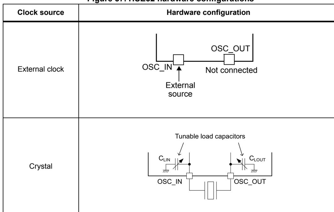
| Clock source | Hardware configuration |
|---|---|
| External clock | |
| Crystal |
12.4.2 HSI16 clock
The HSI16 clock signal is generated from an internal 16 MHz RC oscillator.
The HSI16 RC oscillator has the advantage of providing a clock source at low cost. It also has a faster startup time than the HSE32 crystal oscillator. However, even with calibration, the frequency is less accurate than an external crystal oscillator.
The HSI16 clock is used as the system clock after reset and wake-up from Stop and Standby modes. It can also be used as a backup clock source (auxiliary clock) for the CPU if the HSE32 crystal oscillator fails. Refer to Section 12.4.8: HSE32 clock security system (HSECSS) .
The HSI16 RC oscillator is stable or not. At startup, the HSI16 clock is not released until this bit is set by hardware. The HSI16 RC oscillator is stable or not. At startup, the HSI16 clock is not released until this bit is set by hardware.
The HSI16 RC can be switched on and off using the HSION bit in the RCC clock control register (RCC_CR) .
Calibration
The RC oscillator frequencies may vary from one chip to another due to manufacturing process variations, which is why each device is factory-calibrated by STMicroelectronics for 1 % accuracy at \( T_A = 30^\circ\text{C} \) .
After reset, the factory calibration value is loaded in the HSICAL bits in the RCC internal clock sources calibration register 3 (RCC_ICSCR3) .
If the application is subject to voltage or temperature variations, this may affect the RC oscillator speed. The HSI16 frequency can be trimmed in the application using the HSITRIM in the RCC internal clock sources calibration register 3 (RCC_ICSCR3) .
For more details on how to measure the HSI16 frequency variation, refer to Section 12.4.20 .
12.4.3 PLL1
The RCC features one PLL1 that is generally used to provide clocks to the CPU and to some peripherals. The PLL1 must be enabled only in range 1 and range 1.5. The PLL must be disabled before entering range 2.
The PLL1 integrated in the RCC offers the following features:
- • Input frequency range: 4 to 16 MHz
- • VCO frequency range: 128 to 544 MHz
- • Integer and fractional modes
- • A 13-bit sigma-delta ( \( \Sigma\Delta \) ) modulator for fine-tuning the VCO frequency by steps of 11 to 0.3 ppm
The \( \Sigma\Delta \) modulator can be updated on the fly, without generating frequency overshoots on PLL1 outputs.
- • Three outputs with postdividers
The PLL1 is controlled via the RCC_PLL1DIVR, RCC_PLL1FRACR, RCC_PLL1CFGR, and RCC_CR registers.
The frequency of the reference clock provided to the PLL1 ( \( F_{\text{ref\_ck}} \) ) must range between 4 and 16 MHz. The user application must program the PLL1M dividers properly in the RCC PLL1 configuration register (RCC_PLL1CFGR) to match this condition. Additionally, PLL1RGE must be set according to the reference input frequency to ensure an optimal performance of the PLL1.
To reduce power consumption, it is recommended to configure the VCO output to the lowest possible frequency.
The PLL1N loop divider must be programmed to achieve the expected frequency at VCO output. In addition, the VCO output range (128 to 544 MHz) must be respected.
The PLL1 operates in integer mode when PLL1FRACEN is 0 and the PLL is enabled with PLL1ON. Fractional mode can be enabled at any time by setting PLL1FRACN to the required value, and subsequently setting the PLL1FRACEN bit. The \( \Sigma\Delta \) modulator is designed to minimize the jitter impact while allowing very-small-step frequency adjustments. To update the fractional value, first clear the PLL1FRACEN bit before updating the PLL1FRACN value, and subsequently set PLL1FRACEN again. The old PLL1FRACN value is used until the new value is activated by setting PLL1FRACEN. PLL1FRACN can be updated by software only when PLL1FRACEN has been cleared.
The PLL1 can be enabled by setting PLL1ON to 1 in the RCC clock control register (RCC_CR) . The PLL1RDY bit indicates that the PLL1 is ready (meaning locked).
Note: Before enabling the PLL1, make sure that the reference frequency ( \( F_{\text{ref\_ck}} \) ) provided to the PLL1 is stable.
The hardware prevents writing PLL1ON to 0 if the PLL1 is currently used to deliver the system clock.
The following PLL1 parameters cannot be changed once the PLL1 is enabled: PLL1M, PLL1SRC, PLL1N, PLL1RGE, PLL1P, PLL1Q, and PLL1R.
To insure an optimal behavior of the PLL1 when one of the postdividers (PLL1P, PLL1Q, or PLL1R) is not used, the application must clear the enable bit (PLL1PEN, PLL1QEN, or
PLL1REN), and, preferably, also the corresponding postdivider field (PLL1P, PLL1Q, or PLL1R).
If the above rules are not respected, the PLL1 output frequency is not ensured.
Output frequency computation
When the PLL1 is operated in integer mode, the VCO frequency ( \( F_{VCO} \) ) is given by the following formula:
When the PLL1 is operated in fractional mode, it is possible to change the value of the PLL1FRACN on the fly without disturbing the PLL1 output. This feature can be used either to generate a specific frequency from any crystal value with a good accuracy, or to fine-tune the frequency on the fly.
For PLL1, the VCO frequency is given by the following formula:
For both integer and fractional mode, the PLL1 output frequency is given by the formula below:
The PLL1 is disabled by hardware when:
- • The system enters Stop or Standby mode.
- • A HSE32 failure occurs, and PLL1, clocked by HSE32, is used as the system clock.
The fractional information used by the PLL is reset when disabling the PLL.
PLL1 initialization phase
Here below the recommended PLL1 initialization sequence in integer and fractional mode (PLL1 is supposed to be disabled at the start of the sequence):
- 1. Initialize the PLL1 registers according to the required frequency.
- – For integer mode, clear PLL1FRACEN.
- – For fractional mode, set PLL1FRACN to the required initial value and then set PLL1FRACEN.
- 2. Once the PLL1ON bit is set, the application must wait until the PLL1RDY bit is set. As long as PLL1RDY = 0, the PLL1FRACEN bit must not be altered.
- 3. When the PLL1RDY bit is set, the PLL1 is ready to be used.
- 4. If the application intends to tune the PLL1 frequency on the fly:
- a) PLL1FRACEN must be cleared so the PLL1FRACN value can be updated while the PLL is running.
- b) A new value can be set in PLL1FRACN.
- c) PLL1FRACEN must be set to activate the newly programmed value in PLL1FRACN and for the PLL to take it into account.
Note: When the PLL1RDY is set, it means that the difference between the PLL1 output frequency and the target value is less than 2 %.
12.4.4 LSE clock
The LSE crystal is a 32.768 kHz low-speed external crystal or ceramic resonator. It has the advantage of providing a low-power but highly accurate clock source to the real-time clock peripheral (RTC) for clock/calendar, the 2.4 GHz RADIO sleep timer, or other timing functions.
The LSE crystal is switched on and off using the LSEON bit in RCC backup domain control register (RCC_BDCR1) . If the LSE is used by other peripherals or functions than RTC and TAMP, the LSESYSEN bit must also be set in the RCC backup domain control register (RCC_BDCR1) (refer to LSE when used by peripherals other than RTC/TAMP and RCC functions ).
The crystal oscillator driving strength can be changed at runtime using the LSEDRV[1:0] bits to obtain the best compromise between robustness and a short startup time on the one hand and low-power consumption on the other. The LSE drive can be decreased to a lower-drive capability when the LSE is ON. However, once LSEDRV is selected, the drive capability cannot be increased if LSEON = 1.
The LSERDY flag in the RCC backup domain control register (RCC_BDCR1) indicates whether the LSE crystal is stable or not. At startup, the LSE crystal output clock signal is not released until this bit is set by hardware. An interrupt can be generated if enabled in the RCC clock interrupt enable register (RCC_CIER) .
In addition, glitches on the LSE can be filtered by setting LSEGFON. LSEGFON must be written when the LSE is disabled (LSEON = 0 and LSERDY = 0).
The LSE oscillator can be trimmed using the LSETRIM trimming bits in the RCC backup domain control register (RCC_BDCR1) . After a BOR0 reset and loading option bytes using the OBL_LAUNCH register bit when the SBF is cleared, the factory trimmed values are loaded in the LSETRIM bits, which can subsequently be modified by the application software.
External source (LSE bypass)
In this mode, an external clock source must be provided. It can have a frequency of up to 1 MHz. This mode is selected by setting the LSEBYP and LSEON bits in the RCC backup domain control register (RCC_BDCR1) . The external clock signal (square, sinus, or triangle), with ~50 % duty cycle, must drive the OSC32_IN pin while the OSC32_OUT pin can be used as a GPIO (see Figure 38 ).
Figure 38. LSE 32 clock sources
| Clock source | Hardware configuration |
|---|---|
| External clock | 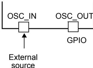 |
| Crystal/ceramic resonators |  |
LSE when used by peripherals other than RTC/TAMP and RCC functions
By default, when enabled by LSEON, the LSE is sent only to RTC and TAMP (assuming that RTCSEL = 01).
If the LSE is needed for other peripherals (such as the peripheral clock or a trigger source) or if the LSE is used by an RCC function (such as LSCO or MCO), the lsesys clock must be enabled with LSESYSEN by following the sequence below:
- 1. Wait until the LSE clock is ready and the LSEON bit is set, so the LSERDY is set in the RCC backup domain control register (RCC_BDCR1) .
- 2. Set the LSESYSEN bit in the RCC_BDCR1 register.
- 3. Wait until the lsesys clock is ready (LSESYSRDY = 1 in RCC_BDCR1).
The LSE power consumption is increased when LSESYSEN = 1.
12.4.5 LSI clock
The low-power LSI clock can be kept running in Stop and Standby modes for the IWDG, and in Stop 0, 1, 2, and Standby modes for the RTC and TAMP. The LSI clock is generated from two sources
- • LSI1 RC low-power oscillator
- • LSI2 RC low-drift oscillator selection between LSI1 or LSI2 is done by the LSI2ON bit. Whenever LSI2 is enabled (LSI2ON = 1) and LSI2 is ready (LSY2RDY = 1), the LSI clock is generated by LSI2. Else, LSI1 is selected as the LSI clock source (not available on STM32WBA25/23 devices).
Table 108. LSI clock selection
| LSI1ON/LSI1RDY | LSI2ON/LSI2RDY | LSI clock |
|---|---|---|
| 0/0 | 0/0 | No clock |
| 1/1 | 0/0 | LS1 RC source |
| 0/0 | 1/1 | LSI2 RC source |
| 1/1 | 1/1 | LSI2 RC source |
When the IWDG is started, the LSI clock is forced on and cannot be disabled. When both the LSI1 and LSI2 are disabled, LSI1 is forced on. When LSI select LSI2 RC source, the LSI1 RC source can be disabled.
LSI1 low-power
Caution: The LSI1 must not be used for the 2.4 GHz RADIO sleep timer.
The LSI1 RC can be switched on and off using the LSI1ON bit in the RCC backup domain control register (RCC_BDCR1) .
The LSI1RDY flag in the RCC backup domain control register (RCC_BDCR1) indicates if the LSI1 oscillator is stable or not. At startup, the clock is not released until this bit is set by hardware. An interrupt can be generated if enabled in the RCC clock interrupt enable register (RCC_CIER) .
The clock frequency is either ~32 kHz or ~250 Hz, depending on the LSI1PREDIV bit in the RCC backup domain control register (RCC_BDCR1) . Setting LSI1PREDIV results in lower consumption (refer to the electrical characteristics section of the datasheet for more details).
Note: When the IWDG is enabled or when the RTC or TAMP is clocked by the LSI, the LSI1PREDIV can no longer be changed.
LSI2 low-drift (not available on STM32WBA25/23 devices)
The LSI2 RC can be switched on and off using the LSI2ON bit in the RCC Backup domain control register (RCC_BDCR1).
The LSI2RDY flag in the RCC Backup domain control register (RCC_BDCR1) indicates if the LSI2 oscillator is stable or not. At startup, the clock is not released until this bit goes to 1 by hardware. An interrupt can be generated if enabled in the RCC clock interrupt enable register (RCC_CIER). After LSI2 ready, there is an additional delay of up to six clock cycles before clocking a peripheral.
The LSI2 makes possible trimming using the LSI2CFG and LSI2MODE in RCC Backup domain control register (RCC_BDCR2).
- • Use LSI2CFG to select the temperature at which the frequency temperature sensitivity is the lowest
- • Use LSI2MODE to configure the power consumption versus the accuracy. For best performance nominal power consumption and highest accuracy must be selected.
12.4.6 System clock (SYSCLK) selection
Different clock sources can be used to drive the system clock (SYSCLK):
- • HSI16 oscillator
- • HSE32 oscillator
- • pll1rclk
The system clock maximum frequency is 64 MHz. After a system reset, the HSI16 oscillator at 16 MHz is selected as the system clock. When a clock source is used directly or through the PLL as a system clock, it is not possible to stop it.
A switch from one clock source to another occurs only if the target clock source is ready (for instance, the clock is stable after a startup delay). If a clock source that is not yet ready is selected, the switch occurs when the clock source is ready. Status bits in the RCC clock configuration register 1 (RCC_CFGR1) indicate which clocks are ready and which clock is currently used as the system clock.
Table 109 gives the different bus frequencies depending on the product voltage range.
Table 109. SYSCLK and bus maximum frequency
| Product voltage | SYSCLK / AHB1 / AHB2 / AHB4 / AHB5 (1) / APB1 / APB2 / APB7 | AHB5 (2) |
|---|---|---|
| range 1 | ||
| range 1.5 | 64 MHz | 32 MHz |
| range 2 | 16 MHz | 12 MHz |
1. For PTACONV.
2. For 2.4 GHz RADIO.
Note: After reset, voltage scaling range 2 is used with SYSCLK at 16 MHz, hclk5 at 8 MHz and one wait state on FLASH, SRAM1, and SRAM2.
System clock maximum frequency step
When increasing the SYSCLK frequency, the frequency step must be limited. The frequency must be increased in steps using the PLL1RCLKPRE divider and PLL1RCLKPRESTEP divider steps.
A two-step divider makes it possible to limit the maximum frequency step to 43 MHz, which requires at least 1000 cycles of the pll1rclk clock to switch. Two-step division uses an intermediate frequency of pll1rclk/1.75.
A three-step divider limits the maximum frequency step to 29 MHz and requires at least 2000 cycles of the pll1rclk clock to switch. Three-step division uses intermediate frequencies of pll1rclk/2.25 and pll1rclk/1.4.
As an example, to increase the SYSCLK from 16 MHz (HSI16) to 64 MHz (pll1rclk), the following sequence must be used:
- 1. Switch VOS to range 1 and wait for VOSRDY.
- 2. Select PLL1RCLKPRE to divide, and the divider steps in PLL1RCLKPRESTEP.
- 3. Lock PLL1.
- 4. Switch the SYSCLK source from HSI16 to PLL1 in SW.
- 5. Wait for the SYSCLK switch to complete in SWS (SYSCLK = pll1rclk divided).
- 6. Set PLL1RCLKPRE to not divide.
- 7. Wait for PLL1RCLKPRERDY to indicate readiness (SYSCLK = pll1rclk).
Warning: The SYSCLK must be switched to a higher frequency when the incremental frequency step is \( \leq 47 \) MHz, or device operation cannot be ensured. For bigger incremental frequency steps, use the PLL1RCLKPRE division.
When the SYSCLK is selected from PLL1 and PLL1RCLKPRE is changed from divide to not divide, the not divide clock is ready on the SYSCLK after a delay, as detailed in Table 110 .
Table 110. PLL1RCLKPRERDY delay versus pll1rclk frequency
| f PLL1RCLK [MHz] | SYSCLK divider delay when going from divide to not divide [ \( \mu\text{s} \) ] | |
|---|---|---|
| Two-step | Three-step | |
| 64 | 15.63 | 31.25 |
The PLL1RCLKPRE, PLL1RCLKPRERDY, and SYSCLK frequency behavior depends on the SWS and pll1rclk settings, as detailed in Table 111 :
Table 111. PLL1RCLKPRERDY and SYSCLK behavior
| PLL1RCLKPRE | PLL1ON | PLL1RCLKPRERDY | SWS | SYSCLK | Description |
|---|---|---|---|---|---|
| 0 | x | 1 | Not PLL1 | Other than pll1rclk | SWS, select other source then PLL1 |
| 1 | x | 0 | |||
| 1 | 1 | x | PLL1 | pll1rclk | SYSCLK = pll1rclk divided |
| 0 | 1 | 0 | SYSCLK = pll1rclk divided. | ||
| 0 | 1 | 1 | SYSCLK = pll1rclk not divided |
System clock frequency change and hclk5
When increasing the SYSCLK frequency above 32 MHz, the hclk5 division ratio in HPRE5 must be adapted to keep the hclk5 frequency \( \leq 32 \) MHz.
Warning: The AHB5 clock frequency for the 2.4 GHz RADIO must never exceed 32 MHz. When this is not respected, device operation cannot be ensured.
For this purpose HPRE5 must be written by software with the divider value corresponding to the \( f_{PLL1RCLK} \) frequency, before switching the system clock to the PLL1 source in SW. The written HPRE5 value is used by the hardware to divide the SYSCLK, at the same time as the SYSCLK clock switch to the PLL1 source.
- 1. Lock PLL1.
- 2. Optional: select PLL1RCLKPRE to divide.
- 3. Set the HPRE5 value to be used with the \( f_{PLL1RCLK} \) frequency.
- 4. Switch the SYSCLK source to pll1rclk in SW.
- 5. Wait for the SYSCLK switch to complete in SWS ( \( hclk5 = f_{PLL1RCLK}/HPRE5 \) ).
When decreasing the SYSCLK frequency from a frequency above 32 MHz from the PLL1 source to the HSE32 or HSE16 source, the hclk5 is set to not divide by hardware.
- 1. Switch the SYSCLK source away from PLL1.
- 2. Wait for the SYSCLK switch to complete in SWS (SYSCLK = HSI16 or HSE32, hclk5 = SYSCLK/HDIV5).
The software-written HPRE5 value takes effect only when the SYSCLK has been switched to pll1rclk in SWS.
When SW = PLL1 and SWS = not PLL1, write operations to HPRE5 are ignored.
Note: The HPRE5 divider is not used when the SYSCLK source is HSE32, HSE32 divided by 2, or HSI16 (SWS = not pll1rclk).
In range 2, the hclk5 frequency must be kept at \( \leq 8 \) MHz. Before entering range 2, HDIV5 must select “divide by 2”.
When moving from range 1 or range 1.5 to range 2:
- 1. Set HDIV5 to divide by 2.
- 2. Switch the SYSCLK source to HSE32 divided by 2 or HSI16.
- 3. Wait for the SYSCLK switch to complete in SWS.
- 4. Select range 2 in VOS in the PWR_VOSR register.
- 5. Optionally, wait until the ACTVOS in PWR_VMMSR = VOS in PWR_VOSR, and the ACTVOSRDY flag is set in PWR_VMMSR.
When changing from range 2 to range 1 or range 1.5:
- 1. Select range 1 or range 1.5 in VOS in PWR_VOSR.
- 2. Wait until the VOSRDY flag is set in PWR_VOSR.
- 3. Optionally, clear HDIV5 to no longer divide by 2.
Note: When entering Stop 1, 2, and 3 mode, hardware sets the hclk5 frequency to divide by 2 in HDIV5.
Note: The HDIV5 divider is not used when the SYSCLK source is PLL1 (SWS = PLL1).
Note: When 2.4 GHz RADIO is active, the device must be in range 1 or range 1.5, hclk5 must be \( \geq 16 \) MHz, and HDIV5 must be cleared.
12.4.7 Clock source frequency versus voltage scaling
Table 112. Clock source maximum frequency
| Product voltage | HSI16 | HSE32 | PLL1 output (VCO min and max) |
|---|---|---|---|
| Range 1 | Allowed | Allowed | 64 MHz |
| Range 1.5 | (128 - 544 MHz) | ||
| Range 2 | Allowed (divided by 2) | Not allowed |
12.4.8 HSE32 clock security system (HSECSS)
The HSECSS can be activated by software with the HSECSSON bit. In this case, the clock detector is enabled after the HSE32 oscillator wake-up time and disabled when this oscillator is stopped.
The HSECSS makes it possible to detect the absence of a clock. Refer to the device datasheet for more information.
If a failure is detected on the HSE32 clock, the HSE32 oscillator is automatically disabled. A clock failure event is sent to several timers break input and an interrupt is generated to inform the software about the failure (HSECSSI: clock security system interrupt). This allows the MCU to perform rescue operations. The HSECSSI is linked to the Core NMI (nonmaskable interrupt) exception vector.
Once the HSECSS has been enabled and if the HSE32 clock fails, the HSECSSI occurs and an NMI is automatically generated. The NMI is executed indefinitely, unless the pending HSECSSI bit is cleared. Consequently, the user must clear the HSECSSI bit in the NMI ISR by setting the HSECSSC bit in the RCC clock interrupt clear register (RCC_CICR) .
If the HSE32 oscillator is used directly or indirectly as the system clock (indirectly meaning it is used as the PLL1 input clock and the pll1rclk clock is used as the system clock), a detected failure causes a switch of the system clock to the HSI16 oscillator and the disabling of the HSE32 oscillator. If the HSE32 clock and PLL1 are used as system clock when the failure occurs, the PLL1 is disabled too.
12.4.9 LSE clock security system on (LSECSS)
A clock security system on the LSE can be activated by software setting the LSECSSON bit in the RCC backup domain control register (RCC_BDCR1) . This bit can be disabled only by a hardware reset or RTC software reset, or after a failure detection on LSE. LSECSSON must be written after LSE is enabled (LSEON set) and ready (LSERDY set by hardware) and after the RTC clock has been selected by RTCSEL.
The LSECSS is working in all modes except Standby.
The clock security system on the LSE detects when the LSE disappears or in case of overfrequency. In addition, the glitches on LSE can be filtered by setting LSEGFON. LSEGFON must be set when LSE is disabled (LSEON = 0 and LSERDY = 0).
If a failure is detected on the external 32 kHz oscillator, the LSE clock is no longer clocking and no hardware action is made to register settings.
In case of an LSECSS detection event (LSECSSD = 1 in the RCC_BDCR1), the software must disable the LSECSSON bit, stop the defective 32 kHz oscillator (disabling LSEON)
and change the low-power clock source (no clock or LSI or HSE32), or take any required action to secure the application.
The LSECSS detection event is connected to the internal tamper 3 of the TAMP peripheral. The internal tamper 3 must be enabled (ITAMP3E = 1 in TAMP_CR1 register) and the associated interrupt enabled (ITAMP3IE in TAMP_IER) to enable wake-up from the low-power modes.
An LSECSS detection event also erases the TAMP backup registers and backup SRAM unless ITAMP3NOER = 1 in the TAMP_CR3 register (see Section 34: Tamper and backup registers (TAMP) for more details).
Refer to the product datasheet for LSECSS electrical characteristics.
12.4.10 ADC kernel clock
The ADC kernel clock source is selected with the ADCSEL bit in the RCC peripherals independent clock configuration register 3 (RCC_CCIPR3) .
If the application requires that the ADC is precisely triggered by a (LP)TIM without any uncertainty, the hclk must be selected as the ADC kernel clock source. The other clock sources are asynchronous to (LP)TIM, so an uncertainty of the trigger instant is added by the resynchronization between the two clock domains.
12.4.11 RTC and TAMP kernel clock
The RTC kernel clock source is used by RTC and TAMP and can be either the HSE32/32, LSE, or LSI clock. It is selected by programming the RTCSEL bits in the RCC backup domain control register (RCC_BDCR1) . This selection cannot be modified without resetting the backup domain. For the RTC to operate properly, the RTC bus clock, pclk, must always be set to a frequency that is greater than or equal to that of the RTC kernel clock.
The TAMP does not require a kernel clock if only the backup registers are used, with tamper in edge detection mode. All other tamper detection modes require a kernel clock (refer to Section 34: Tamper and backup registers (TAMP) for more details).
The LSE and LSI clocks are in the backup domain, whereas the HSE32 clock is not. Consequently:
- • If LSE or LSI is selected as the RTC or TAMP clock, these peripherals continue to work in Stop 0, 1, 2, and Standby modes, provided the RTCRSB is enabled and V DD supply is maintained.
The RTC and TAMP are not functional in Stop 3 mode. When RTC and TAMP use LSI or LSE, they are reset when gating off the clock.
- • If the HSE32 clock is used as the RTC or TAMP clock, these peripherals work only in Run and Sleep modes. They stop working in Stop and Standby modes. Depending on the TAMP configuration, they can remain functional if used in a mode that does not need a kernel clock.
When the RTC and TAMP clock is LSE or LSI, the RTC and TAMP remain clocked and functional under system reset.
If the LSE is needed only for the RTC or TAMP, LSESYSEN must be kept at reset value to get the lowest consumption.
12.4.12 2.4 GHz RADIO bus clocks
The 2.4 GHz RADIO bus clock can be enabled by software with the RADIOEN and RADIOSMEN bits, and by hardware on a 2.4 GHz RADIO sleep timer wake-up event by the STRADIOCLKON bit. Before accessing the 2.4 GHz RADIO sleep timer registers, the bus clock must be ready, indicated by the RADIOCLKRDY register bit.
Table 113. 2.4 GHz RADIO bus clock control
| Device state | CPU state | RADIOEN | RADIOSMEN | STRADIOCLKON | 2.4 GHz RADIO state | 2.4 GHz RADIO bus clock |
|---|---|---|---|---|---|---|
| X | X | 0 | X | 0 | X | Off |
| Run | RUN | 1 | X | X | X | On |
| X | X | 1 | X | On | ||
| Sleep | SLEEP | 1 | 0 | 0 | X | Off |
| 1 | 1 | 0 | ACTIVE | On | ||
| X | X | 1 | SLEEP/DEEPSLEEP | Off | ||
| Stop 0 | DEEPSLEEP | 1 | 0 | 0 | X | Off |
| 1 | 1 | 0 | ACTIVE | On | ||
| X | X | 1 | SLEEP/DEEPSLEEP | Off | ||
| Stop 1 (1) | DEEPSLEEP | X | X | 0 | SLEEP/DEEPSLEEP | Off |
| Stop 2 (1)(3) | DEEPSLEEP | Off | ||||
| Stop 3 (1)(3) | DEEPSLEEP (2) | Off | ||||
| Standby (1)(3) | RESET | DEEPSLEEP/POWER DOWN | Off |
1. When 2.4 GHz RADIO state is ACTIVE or STRADIOCLKON is 1, the device does not enter Stop 1, Stop 2, Stop 3, and Standby modes.
2. The RADIO sleep timer is also stopped.
3. When 2.4 GHz RADIO state is SLEEP, the device does not enter Stop 2, Stop 3, and Standby modes.
When exiting from a low-power mode and the 2.4 GHz RADIO bus clock has been stopped, the RADIOCLKRDY bit must be rechecked before accessing the 2.4 GHz RADIO registers.
The 2.4 GHz RADIO bus clock is kept active only in low-power modes, when STRADIOCLKON is set and/or RADIOEN and RADIOSMEN are set, and the 2.4 GHz RADIO is active.
12.4.13 2.4 GHz RADIO kernel clocks
The 2.4 GHz RADIO has different kernel clocks:
- • Baseband kernel clock
- • Sleep timer low-power clock
The 2.4 GHz RADIO baseband kernel clock is enabled by the BBCLKEN register bit. This clock has the HSE32 as its clock source. For this purpose, the HSE32 oscillator is enabled by hardware on a 2.4 GHz RADIO sleep timer wake-up event setting the STRADIOCLKON register bit, or by software setting the HSEON register bit. When the 2.4 GHz RADIO no longer needs the HSE32 and bus clocks, software must clear the BBCLKEN and STRADIOCLKON bits. If HSE32 is not used by any other function, it must also clear the HSEON bits.
Figure 39. Radio control
The diagram illustrates the clock control logic for the 2.4 GHz RADIO. On the left, various clock sources are shown: 'others' (HSI16), 'OSC HSI16', 'OSC_OUT' (HSE32 OSC 32 MHz), and 'OSC_IN' (HSE CSS). The 'others' and 'OSC HSI16' sources feed into a multiplexer labeled 'sysclk'. The 'HSE32 OSC 32 MHz' and 'HSE CSS' sources feed into a block labeled 'HSE32'. The 'HSE32' block has an 'enable' input and outputs 'HSE32' and 'HSE_RF'. The 'sysclk' output from the multiplexer goes to 'CPU hclk'. The 'HSE32' output goes to 'to 2.4 GHz RADIO kernel clock' through an 'EN' block labeled 'BBCLKEN'. The 'HSE_RF' output goes to 'to 2.4 GHz RADIO RF clock'. There are two 'OR' gates. The first 'OR' gate takes 'STRADIOCLKON' and 'RADIOEN' as inputs and its output goes to an 'EN' block labeled 'HPRE5', which then outputs 'to 2.4 GHz RADIO (hclk5)'. The second 'OR' gate takes 'HSEON' and 'RADIOEN' as inputs and its output goes to an 'EN' block, which then outputs 'to sysclk mux'. The diagram is labeled 'MSV55677V2' in the bottom right corner.
In range 2, the 2.4 GHz RADIO baseband kernel clock is divided by 4 by the hardware. The 2.4 GHz RADIO baseband kernel clock must be enabled to access the 2.4 GHz RADIO RXTX RAM or sequence RAM.
Moreover, the 2.4 GHz RADIO bus clock (hclk5) is enabled by hardware through the STRADIOCLKON bit, independently from the RADIOEN and RADIOSMEN bits. When the 2.4 GHz RADIO no longer needs its bus clock, software must clear the STRADIOCLKON bit. The STRADIOCLKON bit also keeps the 2.4 GHz RADIO bus clock and baseband kernel clock active when entering low-power modes.
Outside any scheduled radio activity, when in Run mode, software can enable the 2.4 GHz RADIO bus clock through the RADIOEN and RADIOSMEN register bits. In this case, the RADIOSMEN bit keeps the 2.4 GHz RADIO bus clock and baseband kernel clock active when entering low-power modes.
The 2.4 GHz RADIO sleep timer kernel clock source can be either the HSE32/1000, LSI, or LSE clock. LSI must be used only when its source is LSI2. It is selected by setting the RADIOSTSEL bits in the RCC backup domain control register (RCC_BDCR1) .
12.4.14 Timer kernel clock
The timer (TIM) kernel clock frequency is derived from the bus clock pclk. The frequency is automatically defined by hardware:
- • If the APB prescaler equals 1, the timer clock frequencies are set to the APB domain frequency (kernel clock frequency = pclk frequency)
- • If the APB prescaler does not equal 1, the timer clock frequencies are set to twice ( \( \times 2 \) ) the APB domain frequency (kernel clock frequency = \( 2 \times \) pclk frequency)
12.4.15 Independent watchdog kernel clock
The independent watchdog uses the LSI as the kernel clock.
If the independent watchdog (IWDG) is started by either user option bytes or software and the LSI clock is disabled (LSI1ON and LSI2ON are cleared), the LSI1 oscillator is forced on. After the LSI oscillator ready delay, the LSI clock is provided to the IWDG.
12.4.16 USB kernel clock
The USB uses the pll1pclk at 48 MHz as the kernel clock. Both the HSE32 and PLL1 shall be enabled.
12.4.17 XSPI feedback clock delay
The XSPI1 feedback clock delay is performed by the DLYBXS1 delay block. It allows for a delay to be added to the XSPI1 feedback clock (refer to Section 21: Delay block (DLYB) ).
12.4.18 SysTick calibration value register
The Cortex ® -M33 core with the TrustZone ® security extension embeds two SysTick timers.
When TrustZone ® is activated, the following SysTick timers are available:
- • SysTick, secure instance
- • SysTick, nonsecure instance
When TrustZone ® is disabled, only one SysTick timer is available.
The Cortex ® -M33 SysTick timer calibration value (STCALIB) is 0x3E8. It gives a reference time base of 1 ms based on a SysTick clock frequency of 1 MHz. To match the 1 ms time base for an application running at a given frequency, the SysTick reload value must be programmed as follows in the Cortex ® -M33 SYST_RVR register:
- • When the SysTick clock source is the CPU clock hclk1
Reload value = ( \( f_{HCLK1} \times STCALIB \) ) - 1 - • When the SysTick clock source is an external clock (hclk1 divided by 8)
Reload value = \( ((f_{HCLK1}/8) \times STCALIB) - 1 \)
Example: the SysTick clock source is the CPU clock hclk1 at 100 MHz, to match a time base of 1 ms:
Note: When using debug Stop mode (DBG_STOP), before the CPU enters DeepSleep it is considered good practice to have software disable the SysTick.
12.4.19 Clock-out capability
• MCO
The microcontroller clock output (MCO) capability allows the clock to be output onto the external MCO pin. One of the following clock signals can be selected as the MCO clock:
- – Active in Run, Sleep, and Stop 0, 1, and 2 modes:
- - LSI
- - LSE
- - HSI16 (in Stop 0, 1, and 2 modes only when an autonomous peripheral kernel clock request is active, or when enabled by HSIKERON)
- - HSE32 (in Stop 0 mode only when the 2.4 GHz RADIO kernel clock request is active)
- - SYSCLKpre (in Stop 0 mode when an autonomous peripheral, other than the 2.4 GHz RADIO, bus clock request is active)
- - hclk5 (when enabled by RCC_AHB5CR.RADIOEN, and in Stop 0 mode when the 2.4 GHz RADIO kernel clock request is active)
- – Active only in Run and Sleep modes:
- - pll1pclk
- - pll1qclk
- - pll1rclk
The selection is controlled by the MCOSEL bits in the RCC clock configuration register 1 (RCC_CFGR1) . The selected clock can be divided with the MCOPRE field in the RCC clock configuration register 1 (RCC_CFGR1) .
The MCO clock output requires the corresponding GPIO pin alternate function to select MCO.
• LSCO
Slow clock output (LSCO) allows one of the low-speed clocks to be output onto the external LSCO pin:
- – LSI
- – LSE
This output remains available in all Run, Sleep, Stop, and Standby modes. The selection is controlled by the LSCOSEL bit and enabled with the LSCOEN bit in the RCC backup domain control register (RCC_BDCR1) .
12.4.20 Internal/external clock measurement
The HSI16 and LSI frequency can be measured indirectly by the TIM16 or TIM17 channel 1 input capture and LPTIM1 or LPTIM2 channel 2 input capture.
HSI16 calibration using LSE
The primary purpose of connecting the LSE to the channel 1 input capture of TIM16 and TIM17 to the channel 2 input capture of LPTIM1 is to be able to measure the HSI16 frequency precisely. When using TIM16 or TIM17 for this purpose, the HSI16 must be used as the system clock source.
The number of HSI16 clock counts between two edges of the LSE signal provides a measure of the internal clock period. Taking advantage of the high precision of the LSE
crystal (typically a few hundred ppm), the internal clock frequency can be determined with a similar resolution, depending on the measurement time. The HSI16 can be trimmed to compensate for the process, temperature, and/or voltage-related frequency deviations.
The basic concept consists of providing a relative measurement (such as the HSI16/LSE ratio). The precision is therefore closely related to the ratio between the two clock sources: the higher the ratio, the better the measurement.
The HSI16 oscillator has dedicated user-accessible calibration bits (HSITRIM) for this purpose.
HSI16 calibration using HSE32
The HSE32 must be used as the system clock and the timer input capture must be connected to HSI16/256. TIM16 and TIM17 channel 1 input capture, as well as the LPTIM2 input capture 2, are connected to the divided oscillator only when TIMICSEL is set in the RCC peripherals independent clock configuration register 1 (RCC_CCIPR1) .
LSI calibration using HSE32
The calibration of the LSI follows the same principle as the HSI16 calibration, but with a change of the reference clock. The LSI clock must be connected to the channel 1 input capture of TIM16 or TIM17, or to the channel 2 input capture of LPTIM1. Then, HSE32 must be defined as the system clock source. The number of HSE32 clock counts between edges of the LSI signal provides a measure of the internal low-speed clock period.
The basic concept consists of providing a relative measurement (such as the HSE32/LSI ratio). The precision is therefore closely related to the ratio between the two clock sources: the higher the ratio, the better the measurement.
12.4.21 Audio synchronization
The audio synchronization system is used to provide capture compare information between the Bluetooth® LE radio packet timing and audio clock.
- • 20-bit programmable free-running upcounter
- • Autoreload
- • Clock prescaler
- • Compare
- • Input capture
- • Capture period
- • Interrupt:
- – Input capture
- – Compare
- – Compare error
- – Autoreload
Before enabling the audio synchronization counter, the autoreload, clock prescaler, and capture prescaler must be provided.
- • The clock prescaler is used to provide a lower-speed clock to the counter.
- • Autoreload is used to define the audio synchronization counter period.
- • The capture prescaler is used to define the capture period. The capture period is a multiple of the audio synchronization counter period.
A capture value of the counter and the capture prescaler value are updated on the first audio synchronization trigger event in the capture period. Any subsequent audio trigger synchronization events during this capture period are discarded. When enabled, an associated capture event interrupt can be generated.
After enabling the audio synchronization counter in CEN, the capture prescaler only starts counting the capture period after receiving a first synchronization from a Bluetooth® LE radio packet.
A capture error flag is set when no audio trigger synchronization event occurs during the capture period. When enabled, an associated capture error interrupt event can be generated.
The compare can be used to generate an interrupt when the counter reaches the compare value.
Refer to Figure 40: Audi synchronization counter block diagram below for the block diagram.
Figure 40. Audi synchronization counter block diagram
The diagram illustrates the internal architecture of the audio synchronization counter. It features a central Counter block. Above it, an Auto-reload block provides a reload value. To the left, a Clock prescaler receives the audiosync_ker_ck input and feeds into the Counter. Below the Clock prescaler, a Capture prescaler receives the audiosync_itr input and also feeds into the Counter. To the right of the Counter, a Capture block and a Compare block are shown. The Capture block receives input from the Counter and the Capture prescaler, and it connects to an Interrupt block. The Compare block also receives input from the Counter and connects to the same Interrupt block. The Interrupt block generates the audiosync_it output. An AHB bus interface is shown on the left, connected to the Counter and the Interrupt block. The diagram is labeled MSv75935V1 in the bottom right corner.
How to use the audio synchronization counter
In the example in Figure 41 below, the following parameters have been used:
- • Autoreload = R (counter period)
- • Capture prescaler = TP (capture period)
- • Compare = C
Figure 41. Audio synchronization timing example
The diagram shows the timing for audio synchronization. The top signal is audiosync_itr , which generates pulses. Below it is the counter , which counts up to R0 (auto-reload) and then resets. The capture prescaler is set to 0 initially, then 1 , then TP , and finally 0 . The capture register stores values N and M . The audiosync_it signal shows interrupts ARF (auto-reload), CAF (capture), and COF (capture overflow). The ENC signal is the enable for the counter. The counter period is the time between two auto-reload events. The capture period is the time between the first and second audiosync_itr events.
The capture value is updated only for the first audiosync_itr event in the capture period. In the first capture period, counter value N and capture prescaler value 0 are captured. The capture period counter is only started after the very first audiosync_itr event, after enabling the audio synchronization counter with ENC . The other audiosync_itr events during this capture period are discarded. In the next capture period, counter value M and capture prescaler value 0 are captured.
The counter drift is calculated by software as follows:
The trigger event may be delayed due to missing received packets by the 2.4 GHz RADIO. The calculation must compensate for this delay.
Error handling
When no audiosync_itr event has been received during the capture period, a capture error interrupt is generated when enabled.
12.4.22 Peripheral clock gating and autonomous mode
Peripheral clock gating in Run mode
Each peripheral clock can be enabled by setting the corresponding EN bit in the RCC_AHBxENR and RCC_APBxENR registers.
When the peripheral clock is not active, read or write access operations to the peripheral registers are not supported.
The enable bit has a synchronization mechanism to create a glitch-free clock for the peripheral. After the enable bit is set, the clock is active after two cycles of the peripheral bus clock.
Caution: Just after enabling the peripheral clock, the software must wait for these two clock cycles before accessing the peripheral registers.
Peripherals clock gating in Sleep and Stop modes
When a peripheral is enabled in RCC_AHBxENR or RCC_APBxENR registers, its bus and kernel clocks can be automatically gated off when the device is in Sleep and Stop modes, by clearing the peripheral SMEN bit in the RCC_AHBxSMENR or RCC_APBxSMENR register. Both the EN and SMEN bits of the peripheral must be set to keep the peripheral bus and kernel clocks on in Sleep and Stop modes. Moreover, in Stop modes, the peripheral bus and kernel clocks are active only upon peripheral clock requests. This excludes the 2.4 GHz RADIO, which requests its bus clock independently from the setting in the RADIOEN and RADIOSMEN register bits.
The peripheral bus clock runs only in Sleep and Stop 0 modes.
The peripheral kernel clock runs only in Sleep and Stop 0, 1, and 2 modes.
For the 2.4 GHz RADIO, the bus clock runs only in Sleep and Stop 0 modes when the STRADIOCLKON bit is set, or when the 2.4 GHz RADIO is active and RADIOEN and RADIOSMEN are set.
Caution: All peripherals on the same bus, with the SMEN bit set, get a clock when an autonomous peripheral on this same bus requests its clock. Peripherals that are not supposed to be clocked in Stop mode must have their SMEN bit cleared.
Caution: The SMEN bit of the peripheral must be set to allow the generation of an interrupt capable of waking up the device from Sleep and Stop modes. This is not necessary when the peripheral wake-up interrupt is generated through the EXTI (GPIO and PVD).
Peripheral clock gating and autonomous mode in Stop modes
Some peripherals support autonomous mode (refer to Table 114: Autonomous peripherals ). These peripherals can generate a kernel clock request and an AHB/APB bus clock request when they need it, to operate and update their status register even in Stop 0, 1, and 2 modes. Depending on the peripheral configuration, either a DMA request or an interrupt can be associated with the peripheral event.
When the system enters a low-power mode (Stop or Standby) and an autonomous peripheral bus clock request is active, or upon an autonomous peripheral bus clock request during Stop mode, Stop 0 mode is entered and the HSI16 oscillator is kept active or woken up and selected as the SYSCLK. The bus clocks for all peripherals having their clock enabled through the EN and SMEN bits are activated.
Note: As soon as the CPU enters DeepSleep, the system enters Stop mode and the autonomous mode operation peripheral bus clock and SYSCLK is switched to HSI16 at 16 MHz. If autonomous peripheral operation with higher bus clock frequencies is needed, the CPU must enter Sleep mode and keep the system in Run with the configured Run mode SYSCLK clock frequency.
If the autonomous peripheral is configured with DMA requests enabled, a data transfer is performed using the peripheral bus clock. The bus clocks and the HSI16 oscillator are switched off automatically when the transfer is finished and no other peripheral requests its bus clock or HSI16 derived kernel clock.
If the autonomous peripheral is configured with interrupt enabled, the interrupt wakes up the device into Run mode.
The autonomous peripherals are autonomous in Stop 0 mode with the LPDMA1, SRAM1, and SRAM2, and are autonomous in Stop 1 and Stop 2 modes on their kernel clock.
There is no autonomous peripheral operation in Stop 3 mode.
Table 114 shows the list of peripherals with autonomous mode capability.
Table 114. Autonomous peripherals
| Domain | Peripheral | Autonomous (1) | Associated DMA (2) | Associated SRAM (2) | |||
|---|---|---|---|---|---|---|---|
| Stop 0 | Stop 1 | Stop 2 | Stop 3 | ||||
| AHB1, APB1, APB2 | U(S)ART1 | Yes | No | LPDMA1 | SRAM1, SRAM2 | ||
| I2C1 | |||||||
| LPTIM2 | |||||||
| AHB4, APB7 | LPUART1 | Yes | Yes (3) | No | |||
| SPI3 | |||||||
| I2C3 | |||||||
| LPTIM1 | No | ||||||
| ADC4 | |||||||
| AHB5 | 2.4 GHz RADIO + RXTXRAM | Yes (4) | No | - | - | ||
1. Enabled when both the EN and SMEN bits of the peripheral are set.
2. DMA and SRAM are only usable in Stop 0 and Stop 1 modes.
3. Without DMA.
4. Enabled when the 2.4 GHz RADIO STRADIOCLKON and BBCLKEN bits are set and the 2.4 GHz RADIO is active. Available only in Stop 0 range 1 and range 1.5.
For peripherals, the autonomous mode is enabled in Stop modes if both the EN and SMEN bits of the peripheral are set.
For the 2.4 GHz RADIO sleep timer it is operational in Stop 0, 1, and 2 modes and Standby with retention. Waking up from the sleep timer puts the system in Run mode and enables the 2.4 GHz RADIO bus clock. The 2.4 GHz RADIO active mode is enabled by software when, additionally, BBCLKEN bit is set, and allows autonomous operation in Stop 0 range 1 and range 1.5 mode.
If an autonomous peripheral requests its kernel clock in Stop 0, 1, and 2 modes, the internal oscillator (HSI16) is woken up if it was off and the kernel clock is propagated only to the peripheral requesting it, and the EN and SMEN bits of the peripheral are set. When the peripheral releases its kernel clock request, the HSI16 is switched off if no other peripheral requests it. Only the 2.4 GHz RADIO uses the HSE32 as the kernel clock, which is woken up, if it was off, by a 2.4 GHz RADIO each time it is woken up by the sleep timer.
If an autonomous peripheral requests its bus clock in Stop 0, 1, and 2 modes and the EN and SMEN bits of the peripheral are set, the internal oscillator (HSI16) is woken up, if it was off, and the system clock is propagated to all peripherals on the associated AHB bus configured with both the EN and SMEN bits of the peripheral set.
Caution: The bus clock propagates to all peripherals (autonomous and nonautonomous peripherals) on the same AHB bus that have both the EN SMEN bits set.
HSI16 can be forced to remain on in Stop 0, 1, and 2 modes by configuring HSIKERON in the RCC_CR register. In this case, the oscillator is propagated only to the peripheral kernel clocks of the enabled autonomous peripherals, which select this oscillator as the kernel clock. This allows the peripheral baud or conversion rates to increase, as there is no need to wait for the oscillator wake-up time when the peripheral requests its kernel clock.
The LSE or LSI always remains on in Stop modes and can be used as the kernel clock in Stop 0, 1, and 2 modes.
12.5 RCC security and privilege functional description
12.5.1 RCC TrustZone® security protection modes
TrustZone® security is activated by the TZEN user option bit in the FLASH_OPTR register. The RCC can secure RCC configuration and status bits from being modified by nonsecure access operations through the RCC secure configuration register (RCC_SECCFGR) . This prevents nonsecure access to reading or modifying the following features:
- • HSE32, HSECSS, HSI16, LSI, LSE, LSECSS, and LSCO configuration and status bits
- • PLL1, AHB, and APB prescaler configuration and status bits
- • System clock (SYSCLK) source clock selection and status bits
- • MCO clock output configuration bits
- • Remove reset flag RMVF configuration
If SPRIV is set in the RCC privilege configuration register (RCC_PRIVCFGR) , the RCC_SECCFGR register can be written only by secure and privileged access. If SPRIV is cleared in RCC_PRIVCFGR, RCC_SECCFGR can be written only through secure access, privileged or unprivileged.
RCC_SECCFGR can be read through secure, nonsecure, privileged, and unprivileged access.
When a peripheral is configured as secure, its related clock, reset, clock source selection, and clock enable during low-power modes control bits are also secure (refer to Table 115: RCC security configuration summary ).
A peripheral is secure when:
- • For securable peripherals by GTZC1_TZSC (TrustZone® security controller): the SEC security bit in the secure configuration registers corresponding to this peripheral is set.
- • For TrustZone®-aware peripherals: a security feature of this peripheral is enabled through its dedicated bits.
Table 115 summarizes the RCC secured bits following the security configuration bit in the RCC_SECCFGR register.
When one security configuration bit is set, some configuration and status bits are secured. The RCC registers may contain secure and nonsecure bits:
- • Secured bits: read and write operations are allowed only by secure access. Nonsecure read returns 0 and write access operations are ignored. No illegal access event is generated.
- • Nonsecure bits: no restriction. Read and write operations are allowed by both secure and nonsecure access operations.
- • A nonsecure write access to RCC_SECCFGR is ignored and generates an illegal access event. An illegal access interrupt is generated if the RCC illegal access interrupt is enabled in the GTZC1_TZIC registers. RCC_SECCFGR can be read by secure or nonsecure access.
When the TrustZone® security is disabled (TZEN = 0), all registers are nonsecure. RCC_SECCFGR write access operations are ignored.
Table 115. RCC security configuration summary
| Configuration bit in RCC_SECCFGR | Secured bits | Corresponding register |
|---|---|---|
| HSISEC | HSION, HSIKERON, HSIRDY | RCC_CR |
| HSICAL, HSITRIM | RCC_ICSCR3 | |
| HSIRDYIE | RCC_CIER | |
| HSIRDYIF | RCC_CIFR | |
| HSIRDYC | RCC_CICR | |
| HSESEC | HSEON, HSERDY, HSECSSON, HSEPRE | RCC_CR |
| HSERDYIE | RCC_CIER | |
| HSERDYIF, HSECSSF | RCC_CIFR | |
| HSERDYC, HSECSSC | RCC_CICR | |
| HSETRIM | RCC_ECSCR1 | |
| LSISEC | LSI1ON, LSI1RDY, LSI1PREDIV, LSI2ON, LSI2RDY, LSCOSEL, LSCOEN | RCC_BDCR1 |
| LSI2MODE, LSI2CFG | RCC_BDCR2 | |
| LSI1RDYIE | RCC_CIER | |
| LSI1RDYIF | RCC_CIFR | |
| LSI1RDYC | RCC_CICR | |
| LSESEC | LSECSSON, LSECSSD, LSEDRV, LSEBYP, LSERDY, LSEON, LSEGON, LSESYSRDY, LSESYSEN, LSCOSEL, LSCOEN | RCC_BDCR1 |
| LSERDYIE, LSI2RDYIE | RCC_CIER | |
| LSERDYF, LSI2RDYF | RCC_CIFR | |
| LSERDYC, LSI2RDYC | RCC_CICR | |
| SYSCLKSEC | SW, SWS, MCOSEL, MCOPRE | RCC_CFGR1 |
| SYSTICKSEL | RCC_CCIPR1 | |
| VOS | PWR_VOSR |
Table 115. RCC security configuration summary (continued)
| Configuration bit in RCC_SECCFGR | Secured bits | Corresponding register |
|---|---|---|
| PRESCSEC | HPRE, PPRE1, PPRE2 | RCC_CFGR2 |
| PPRE7 | RCC_CFGR3 | |
| HPRE5, HDIV5 | RCC_CFGR4 | |
| PLL1SEC | PLL1SRC, PLL1RGE, PLL1FRACEN, PLL1M, PLL1PEN, PLL1QEN, PLL1REN, PLL1RCLKPRE, PLL1RCLKSTEP, PLL1RCLKPRERDY | RCC_PLL1CFGR |
| PLL1N, PLL1P, PLL1Q, PLL1R | RCC_PLL1DIVR | |
| PLL1FRACN | RCC_PLL1FRACR | |
| PLL1RDY, PLL1ON | RCC_CR | |
| PLL1RDYIE | RCC_CIER | |
| PLL1RDYF | RCC_CIFR | |
| PLL1RDYC | RCC_CICR | |
| RMVFSEC | RMVF | RCC_CSR |
12.5.2 RCC privilege protection modes
By default, after reset, all RCC registers can be read or written with both privileged and unprivileged access, except the RCC privilege configuration register (RCC_PRIVCFGR) , which can be written only with privileged access. RCC_PRIVCFGR can be read by secure and nonsecure, privileged and unprivileged access.
The SPRIV bit in RCC_PRIVCFGR can be written only with secure privileged access. This bit configures the privileged access of all RCC secure functions (as defined by the RCC secure configuration register (RCC_SECCFGR) or by the GTZC1_TZSC for securable peripherals, or by the peripheral itself in the case of TrustZone ® -aware peripherals).
When the SPRIV bit is set in RCC_PRIVCFGR:
- • Writing the RCC secure bits is possible only with privileged access, including RCC_SECCFGR.
- • The RCC secure bits can be read only with privileged access except RCC_SECCFGR and RCC_PRIVCFGR that can be read by privileged or unprivileged access.
- • An unprivileged access to a privileged RCC bit or register is discarded: the bits are read as zero and the write to these bits is ignored (RAZ/WI).
The NSPRIV bit in RCC_PRIVCFGR can be written with privileged access only, secure or nonsecure. This bit configures the privileged access of all nonsecure RCC functions (as defined by RCC_SECCFGR, the GTZC1_TZSC for securable peripherals, or the peripheral itself for TrustZone ® -aware peripherals).
When the NSPRIV bit is set in RCC_PRIVCFGR:
- • Writing the nonsecure RCC bits is possible only with privileged access.
- • The nonsecure RCC bits can be read only with privileged access, except RCC_PRIVCFGR, which can be read with privileged or unprivileged access.
- • An unprivileged access operation to a privileged RCC bit or register is discarded: the bits are read as zero and the write to these bits is ignored (RAZ/WI).
12.6 RCC low-power modes
- • AHB and APB peripheral clocks, including the DMA clock, can be disabled by software.
- • Sleep mode stops the CPU hclk1 clock. The memory interface clocks (flash memory, cache, and all SRAM interfaces) can be stopped by software during Sleep mode. The AHB to APB bridge clocks are disabled by hardware during Sleep mode, when all clocks of the peripherals connected to them are disabled.
- • Stop modes stop all clocks in the core domain and disable the PLL1, HSI16, and HSE32 oscillators. However, HSI16 and HSE32 can be switched on if the peripheral requests it for kernel clock operation purposes, or to generate a wake-up interrupt (see Section 12.4.22: Peripheral clock gating and autonomous mode for more details). LSI and LSE can also remain active in Stop modes.
- • Standby mode stops all the clocks and disables the PLL1, HSI16, and HSE32 oscillators. LSI and LSE can remain active in Standby modes.
Stopping the system clock in Stop and Standby modes can be overridden for debugging by setting the DBG_STOP and/or DBG_STANDBY bits. For more details, refer to Section 41.13.4: Low-power mode emulation .
Note: When using debug Stop mode (DBG_STOP), a SysTick event wakes up the device. It is considered good practice that software disables the SysTick before the CPU enters DeepSleep.
When entering and exiting Stop modes, the system clock is HSI16. The user trim of HSI16 is kept.
When leaving the Standby modes, the system clock is HSI16. The user trim is lost.
If a flash memory programming operation is in progress, Stop and Standby mode entry is delayed until the flash memory interface access operation has finished. If access to the APB domain is ongoing, Stop and Standby mode entry is delayed until the APB access operation has finished. If an autonomous peripheral bus clock request is active, Stop 0 mode is entered. If another low-power mode (Stop or Standby) is selected in LPMS, entry to the selected low-power mode is delayed until the autonomous peripheral bus clock request is released.
12.7 RCC interrupts
Table 116 summarizes the interrupt sources and the way to control them.
Table 116. Interrupt sources and control
| Interrupt vector | Interrupt event flag | Description | Enable control bit | Interrupt clear method | Exit from Sleep mode | Exit from Stop, Standby modes |
|---|---|---|---|---|---|---|
| RCC/RCC_S (1) | LSI1RDYF | LSI1 ready | LSI1RDYIE | Set LSI1RDYC to 1 | Yes | No |
| LSI2RDYF | LSI2 ready | LSI2RDYIE | Set LSI2RDYC to 1 | |||
| LSERDYF | LSE ready | LSERDYIE | Set LSERDYC to 1 | |||
| HSIRDYF | HSI16 ready | HSIRDYIE | Set HSIRDYC to 1 | |||
| HSERDYF | HSE32 ready | HSERDYIE | Set HSERDYC to 1 | |||
| PLL1RDYF | PLL1 ready | PLL1RDYIE | Set PLL1RDYC to 1 | |||
| TAMP | ITAMP3F (2) | LSECSS failure | LSECSSON and ITAMP3E (2) and ITAMP3IE (2) | Set CITAMP3F (2) to 1 | Yes | Yes |
| NMI | HSECSSF | HSECSS failure | HSECSSON (3) | Set HSECSSC to 1 | Yes | No |
| AUDIOSYNC | CAF | Capture event | CAIE | Write CAF to 0 | Yes | No |
| COF | Compare event | COIE | Write COF to 0 | |||
| CAEF | Capture error event | CAEIE | Write CAEF to 0 | |||
| ARF | Auto-reload event | ARIE | Write ARF to 0 |
- 1. The RCC secure interrupt vector is used only when TrustZone ® is enabled.
- 2. The LSECSS failure event (LSECSSD) is connected to the TAMP internal tamper 3. To get the interrupt associated with this event, the internal tamper 3 and its interrupt must be enabled. The ITAMP3F, ITAMP3E, ITAMP3IE, and CITAMP3F bits are in the TAMP peripheral.
- 3. It is not possible to mask this interrupt when the security system feature is enabled (HSECSSON = 1).
12.8 RCC registers
12.8.1 RCC clock control register (RCC_CR)
Address offset: 0x000
Reset value: 0x0000 0500
Access: no wait state; word, half-word, and byte access
| 31 | 30 | 29 | 28 | 27 | 26 | 25 | 24 | 23 | 22 | 21 | 20 | 19 | 18 | 17 | 16 |
|---|---|---|---|---|---|---|---|---|---|---|---|---|---|---|---|
| Res. | Res. | Res. | Res. | Res. | Res. | PLL1RDY | PLL1ON | Res. | Res. | Res. | HSEPR E | HSECS SON | Res. | HSE RDY | HSE ON |
| r | rw | rw | rs | r | rw | ||||||||||
| 15 | 14 | 13 | 12 | 11 | 10 | 9 | 8 | 7 | 6 | 5 | 4 | 3 | 2 | 1 | 0 |
| Res. | Res. | Res. | Res. | Res. | HSIRDY | HSIKERON | HSION | Res. | Res. | Res. | Res. | Res. | Res. | Res. | Res. |
| r | rw | rw |
Bits 31:26 Reserved, must be kept at reset value.
Bit 25 PLL1RDY : PLL1 clock ready flag
Set by hardware to indicate that the PLL1 is locked.
Access to the bit can be secured by RCC PLL1SEC. When secure, nonsecure read/write access is RAZ/WI. It does not generate an illegal access interrupt. This bit can be protected against unprivileged access when secure with RCC SPRIV or when nonsecure with RCC NSPRIV.
0: PLL1 unlocked
1: PLL1 locked (PLL1RDY remains set when PLL1 is selected as sysclk and PLL1 is disabled by HSECSS failure).
Bit 24 PLL1ON : PLL1 enable
Set and cleared by software to enable the main PLL.
Cleared by hardware when entering Stop or Standby modes and when PLL1 on HSE32 is selected as sysclk, on a HSECSS failure.
Access to the bit can be secured by RCC PLL1SEC. When secure, nonsecure read/write access is RAZ/WI. It does not generate an illegal access interrupt. This bit can be protected against unprivileged access when secure with RCC SPRIV or when nonsecure with RCC NSPRIV.
0: PLL1 off
1: PLL1 on
Bits 23:21 Reserved, must be kept at reset value.
Bit 20 HSEPRE : HSE32 clock for SYSCLK prescaler
Set and cleared by software to control the division factor of the HSE32 clock for SYSCLK.
Access to the bit can be secured by RCC HSESEC. When secure, nonsecure read/write access is RAZ/WI. It does not generate an illegal access interrupt. This bit can be protected against unprivileged access when secure with RCC SPRIV or when nonsecure with RCC NSPRIV.
0: HSE32 not divided, SYSCLK = HSE32
1: HSE32 divided, SYSCLK = HSE32/2
Bit 19 HSECSSON: HSE32 clock security system enableSet by software to enable the HSE32 clock security system. When HSECSSON is set, the clock detector is enabled by hardware when the HSE32 oscillator is ready and disabled by hardware if a HSE32 clock failure is detected. This bit is set only and is cleared by reset.
Access to the bit can be secured by RCC HSESEC. When secure, nonsecure read/write access is RAZ/WI. It does not generate an illegal access interrupt. This bit can be protected against unprivileged access when secure with RCC SPRIV or when nonsecure with RCC NSPRIV.
0: HSE32 clock security system off (clock detector off)
1: HSE32 clock security system on (clock detector on if the HSE32 oscillator is stable, off if not).
Bit 18 Reserved, must be kept at reset value. Bit 17 HSERDY: HSE32 clock ready flagSet by hardware to indicate that the HSE32 oscillator is stable. This bit is set both when HSE32 is enabled by software by setting HSEON and when requested as kernel clock by the 2.4 GHz RADIO.
Access to the bit can be secured by RCC HSESEC. When secure, nonsecure read/write access is RAZ/WI. It does not generate an illegal access interrupt. This bit can be protected against unprivileged access when secure with RCC SPRIV or when nonsecure with RCC NSPRIV.
0: HSE32 oscillator not ready
1: HSE32 oscillator ready to be used by the CPU.
Bit 16 HSEON: HSE32 clock enableSet and cleared by software.
Cleared by hardware to stop the HSE32 clock for the CPU when entering Stop and Standby modes and on a HSECSS failure.
When the HSE32 is used as a 2.4 GHz RADIO kernel clock, enabled by RADIOEN and RADIOSMEN, and the 2.4 GHz RADIO is active, HSEON is not cleared when entering a low-power mode. In this case, only Stop 0 mode is entered as a low-power mode.
This bit cannot be reset if the HSE32 oscillator is used directly or indirectly as the system clock.
Access to the bit can be secured by RCC HSESEC. When secure, nonsecure read/write access is RAZ/WI. It does not generate an illegal access interrupt. This bit can be protected against unprivileged access when secure with RCC SPRIV or when nonsecure with RCC NSPRIV.
0: HSE32 oscillator not requested by the CPU.
1: HSE32 oscillator ON
Bits 15:11 Reserved, must be kept at reset value. Bit 10 HSIRDY: HSI16 clock ready flagSet by hardware to indicate that HSI16 oscillator is stable. This bit is set only when HSI16 is enabled by software by setting HSION.
Access to the bit can be secured by RCC HSISEC. When secure, nonsecure read/write access is RAZ/WI. It does not generate an illegal access interrupt. This bit can be protected against unprivileged access when secure with RCC SPRIV or when nonsecure with RCC NSPRIV.
0: HSI16 clock not ready
1: HSI16 clock ready
Note: Once the HSION bit is cleared, HSIRDY goes low after six HSI16 clock cycles.
Bit 9 HSIKERON : HSI16 enable for some peripheral kernels
Set and cleared by software to force the HSI16 oscillator on, even in Stop 0, 1, and 2 modes. Keeping the HSI16 oscillator on in Stop modes allows the communication speed not to be reduced by the HSI16 oscillator startup time. This bit has no effect on the HSION register bit value.
Cleared by hardware when entering Stop 3 and Standby modes.
Refer to Peripheral clock gating and autonomous mode for more details.
Access to the bit can be secured by RCC HSISEC. When secure, nonsecure read/write access is RAZ/WI. It does not generate an illegal access interrupt. This bit can be protected against unprivileged access when secure with RCC SPRIV or when nonsecure with RCC NSPRIV.
0: No effect on HSI16 oscillator
1: HSI16 oscillator forced on even in Stop 0, 1, and 2 modes
Bit 8 HSION : HSI16 clock enable
Set and cleared by software.
Cleared by hardware when entering Stop and Standby modes.
Set by hardware to force the HSI16 oscillator on when exiting Stop and Standby modes.
Set by hardware to force the HSI16 oscillator on in case of clock security failure of the HSE32 crystal oscillator.
This bit is set by hardware if the HSI16 is used directly or indirectly as the system clock.
Access to the bit can be secured by RCC HSISEC. When secure, nonsecure read/write access is RAZ/WI. It does not generate an illegal access interrupt. This bit can be protected against unprivileged access when secure with RCC SPRIV or when nonsecure with RCC NSPRIV.
0: HSI16 oscillator off
1: HSI16 oscillator on
Bits 7:0 Reserved, must be kept at reset value.
12.8.2 RCC internal clock sources calibration register 3 (RCC_ICSCR3)
Address offset: 0x010
Reset value: 0x0010 0XXX
X is factory-programmed.
Access: no wait state; word, half-word, and byte access
Access to this register can be protected by RCC HSISEC and RCC SPRIV or RCC NSPRIV.
| 31 | 30 | 29 | 28 | 27 | 26 | 25 | 24 | 23 | 22 | 21 | 20 | 19 | 18 | 17 | 16 |
|---|---|---|---|---|---|---|---|---|---|---|---|---|---|---|---|
| Res. | Res. | Res. | Res. | Res. | Res. | Res. | Res. | Res. | Res. | Res. | HSITRIM[4:0] | ||||
| rw | rw | rw | rw | rw | |||||||||||
| 15 | 14 | 13 | 12 | 11 | 10 | 9 | 8 | 7 | 6 | 5 | 4 | 3 | 2 | 1 | 0 |
| Res. | Res. | Res. | Res. | HSICAL[11:0] | |||||||||||
| r | r | r | r | r | r | r | r | r | r | r | r | ||||
Bits 31:21 Reserved, must be kept at reset value.
Bits 20:16 HSITRIM[4:0] : HSI16 oscillator trimming
These bits provide an additional user-programmable trimming value that is added to the HSICAL[11:0] bits. It can be programmed to adjust to voltage and temperature variations that influence the frequency of the HSI16.
Bits 15:12 Reserved, must be kept at reset value.
Bits 11:0 HSICAL[11:0] : HSI16 oscillator calibration
These bits are initialized at startup with the factory-programmed HSI16 calibration value.
12.8.3 RCC clock configuration register 1 (RCC_CFGR1)
Address offset: 0x01C
Reset value: 0x0000 0000
Access: 0 ≤ wait state ≤ 2; word, half-word, and byte access
One or two wait states are inserted only if access occurs during a clock source switch.
Access to this register can be protected by RCC SYSCLKSEC and RCC SPRIV, or RCC NSPRIV.
| 31 | 30 | 29 | 28 | 27 | 26 | 25 | 24 | 23 | 22 | 21 | 20 | 19 | 18 | 17 | 16 |
|---|---|---|---|---|---|---|---|---|---|---|---|---|---|---|---|
| Res. | MCOPRE[2:0] | MCOSEL[3:0] | Res. | Res. | Res. | Res. | Res. | Res. | Res. | Res. | Res. | ||||
| rw | rw | rw | rw | rw | rw | rw | |||||||||
| 15 | 14 | 13 | 12 | 11 | 10 | 9 | 8 | 7 | 6 | 5 | 4 | 3 | 2 | 1 | 0 |
|---|---|---|---|---|---|---|---|---|---|---|---|---|---|---|---|
| Res. | Res. | Res. | Res. | Res. | Res. | Res. | Res. | Res. | Res. | Res. | Res. | SWS[1:0] | SW[1:0] | ||
| r | r | rw | rw | ||||||||||||
Bit 31 Reserved, must be kept at reset value.
Bits 30:28 MCOPRE[2:0] : microcontroller clock output prescaler
Set and cleared by software.
It is highly recommended to change this prescaler before MCO output is enabled.
000: MCO divided by 1
001: MCO divided by 2
010: MCO divided by 4
011: MCO divided by 8
100: MCO divided by 16
others: not allowed
Bits 27:24 MCOSEL[3:0] : microcontroller clock output
Set and cleared by software.
0000: MCO output disabled, no clock on MCO
0001: sysclkpre system clock after PLL1RCLKPRE division selected
0011: HSI16 clock selected
0100: HSE32 clock selected
0101: pll1rclk clock selected
0110: LSI clock selected
0111: LSE clock selected
1000: pll1pclck clock selected
1001: pll1qclck clock selected
1010: hclk5 clock selected
others: reserved
Note: This clock output may have some truncated cycles at startup or during MCO clock source switching.
Bits 23:4 Reserved, must be kept at reset value.
Bits 3:2 SWS[1:0] : system clock switch status
Set and cleared by hardware to indicate which clock source is used as system clock.
00: HS116 oscillator used as system clock
01: reserved
10: HSE32 or HSE32/2, as defined by HSEPRE, used as system clock
11: pll1rclk used as system clock
Bits 1:0 SW[1:0] : system clock switch
Set and cleared by software to select system clock source (SYSCLK).
Cleared by hardware when entering Stop and Standby modes
When selecting HSE32 directly or indirectly as system clock and HSE32 oscillator clock security fails, cleared by hardware.
00: HS116 selected as system clock
01: reserved
10: HSE32 or HSE32/2, as defined by HSEPRE, selected as system clock
11: pll1rclk selected as system clock
12.8.4 RCC clock configuration register 2 (RCC_CFGR2)
Address offset: 0x020
Reset value: 0x0000 0000
Access: word, half-word, and byte access
From 0 to 15 wait states are inserted if access occurs when the APB or AHB prescalers values update is on going.
Access to this register can be protected by RCC PRESCSEC and RCC SPRIV or RCC NSPRIV.
| 31 | 30 | 29 | 28 | 27 | 26 | 25 | 24 | 23 | 22 | 21 | 20 | 19 | 18 | 17 | 16 |
|---|---|---|---|---|---|---|---|---|---|---|---|---|---|---|---|
| Res. | Res. | Res. | Res. | Res. | Res. | Res. | Res. | Res. | Res. | Res. | Res. | Res. | Res. | Res. | Res. |
| 15 | 14 | 13 | 12 | 11 | 10 | 9 | 8 | 7 | 6 | 5 | 4 | 3 | 2 | 1 | 0 |
| Res. | Res. | Res. | Res. | Res. | PPRE2[2:0] | Res. | PPRE1[2:0] | Res. | HPRE[2:0] | ||||||
| rw | rw | rw | rw | rw | rw | rw | rw | rw | |||||||
Bits 31:11 Reserved, must be kept at reset value.
Bits 10:8 PPRE2[2:0] : APB2 prescaler
Set and cleared by software to control the division factor of the APB2 clock (pclk2).
0xx: pclk2 = hclk1 not divided
100: pclk2 = hclk1 divided by 2
101: pclk2 = hclk1 divided by 4
110: pclk2 = hclk1 divided by 8
111: pclk2 = hclk1 divided by 16
Bit 7 Reserved, must be kept at reset value.
Bits 6:4 PPRE1[2:0] : APB1 prescaler
Set and cleared by software to control the division factor of the APB1 clock (pclk1).
0xx: pclk1 = hclk1 not divided
100: pclk1 = hclk1 divided by 2
101: pclk1 = hclk1 divided by 4
110: pclk1 = hclk1 divided by 8
111: pclk1 = hclk1 divided by 16
Bit 3 Reserved, must be kept at reset value.
Bits 2:0 HPRE[2:0] : AHB1, AHB2, and AHB4 prescaler
Set and cleared by software to control the division factor of the AHB1, AHB2, and AHB4 clock (hclk1).
Caution: The software must limit the incremental frequency step by setting these bits correctly to ensure that the hclk1 maximum incremental frequency step does not exceed the maximum allowed incremental frequency step (for more details, refer to Table 109: SYSCLK and bus maximum frequency ). After a write operation to these bits and before decreasing the voltage range, this register must be read to be sure that the new value is taken into account.
0xx: hclk1 = SYSCLK not divided
100: hclk1 = SYSCLK divided by 2
101: hclk1 = SYSCLK divided by 4
110: hclk1 = SYSCLK divided by 8
111: hclk1 = SYSCLK divided by 16
12.8.5 RCC clock configuration register 3 (RCC_CFGR3)
Address offset: 0x024
Reset value: 0x0000 0000
Access: word, half-word, and byte access
From 0 to 15 wait states are inserted if access occurs when the APB or AHB prescalers values update is on going.
Access to this register can be protected by RCC PRECSEC and RCC SPRIV or RCC NSPRIV.
| 31 | 30 | 29 | 28 | 27 | 26 | 25 | 24 | 23 | 22 | 21 | 20 | 19 | 18 | 17 | 16 |
|---|---|---|---|---|---|---|---|---|---|---|---|---|---|---|---|
| Res. | Res. | Res. | Res. | Res. | Res. | Res. | Res. | Res. | Res. | Res. | Res. | Res. | Res. | Res. | Res. |
| 15 | 14 | 13 | 12 | 11 | 10 | 9 | 8 | 7 | 6 | 5 | 4 | 3 | 2 | 1 | 0 |
| Res. | Res. | Res. | Res. | Res. | Res. | Res. | Res. | Res. | PPRE7[2:0] | Res. | Res. | Res. | Res. | ||
| rw | rw | rw | |||||||||||||
Bits 31:7 Reserved, must be kept at reset value.
Bits 6:4 PPRE7[2:0] : APB7 prescaler
Set and cleared by software to control the division factor of the APB7 clock (pclk7).
0xx: hclk1 not divided
100: hclk1 divided by 2
101: hclk1 divided by 4
110: hclk1 divided by 8
111: hclk1 divided by 16
Bits 3:0 Reserved, must be kept at reset value.
12.8.6 RCC PLL1 configuration register (RCC_PLL1CFGR)
Address offset: 0x028
Reset value: 0x0000 0000
Access: no wait state; word, half-word, and byte access.
Access to this register can be protected by RCC PLL1SEC and RCC SPRIV or RCC NSPRIV.
| 31 | 30 | 29 | 28 | 27 | 26 | 25 | 24 | 23 | 22 | 21 | 20 | 19 | 18 | 17 | 16 |
|---|---|---|---|---|---|---|---|---|---|---|---|---|---|---|---|
| Res. | Res. | Res. | Res. | Res. | Res. | Res. | Res. | Res. | PLL1R CLKPR ERDY | PLL1R CLKPR ESTEP | PLL1R CLKPR E | Res. | PLL1R EN | PLL1Q EN | PLL1P EN |
| r | rw | rw | rw | rw | rw | ||||||||||
| 15 | 14 | 13 | 12 | 11 | 10 | 9 | 8 | 7 | 6 | 5 | 4 | 3 | 2 | 1 | 0 |
| Res. | Res. | Res. | Res. | Res. | PLL1M[2:0] | Res. | Res. | Res. | PLL1F RACEN | PLL1RGE[1:0] | PLL1SRC[1:0] | ||||
| rw | rw | rw | rw | rw | rw | rw | rw | ||||||||
Bits 31:23 Reserved, must be kept at reset value.
Bit 22 PLL1RCLKPRERDY : sysclkpre not divided ready.
Set by hardware after PLL1RCLKPRE has been set from divided to not divide, to indicate that the pll1rclk not divided is available on sysclkpre.
0: sysclkpre divided
1: sysclkpre not divided ready
Bit 21 PLL1RCLKPRESTEP : pll1rclk clock for SYSCLK prescaler division step selection
Set and cleared by software to control the division step of the pll1rclk clock for SYSCLK.
0: pll1rclk 2-step division
1: pll1rclk 3-step division
Bit 20 PLL1RCLKPRE : pll1rclk clock for SYSCLK prescaler division enable
Set and cleared by software to control the division of the pll1rclk clock for SYSCLK.
0: pll1rclk not divided, sysclkpre = pll1rclk
1: pll1rclk divided, sysclkpre = pll1rclk divided
Bit 19 Reserved, must be kept at reset value.
Bit 18 PLL1REN : PLL1 DIVR divider output enable
Set and cleared by software to enable the pll1rclk output of the PLL1.
To save power, the PLL1REN and PLL1R bits must be set to 0 when the pll1rclk is not used.
0: pll1rclk output disabled
1: pll1rclk output enabled
Bit 17 PLL1QEN : PLL1 DIVQ divider output enable
Set and reset by software to enable the pll1qclk output of the PLL1.
To save power, the PLL1QEN and PLL1Q bits must be set to 0 when the pll1qclk is not used.
0: pll1qclk output disabled
1: pll1qclk output enabled
Bit 16 PLL1PEN : PLL1 DIVP divider output enable
Set and reset by software to enable the pll1pclck output of the PLL1.
To save power, the PLL1PEN and PLL1P bits must be set to 0 when the pll1pclck is not used.
0: pll1pclck output disabled
1: pll1pclck output enabled
Bits 15:11 Reserved, must be kept at reset value.
Bits 10:8 PLL1M[2:0] : Prescaler for PLL1
Set and cleared by software to configure the prescaler of the PLL1. The VCO1 input frequency is PLL1 input clock frequency/PLL1M.
This field can be written only when the PLL1 is disabled (PLL1ON = 0 and PLL1RDY = 0).
000: division by 1 (bypass)
001: division by 2
010: division by 3
...
111: division by 8
Bits 7:5 Reserved, must be kept at reset value.
Bit 4 PLL1FRACEN : PLL1 fractional latch enable
Set and reset by software to latch the content of PLL1FRACN into the \( \Sigma\Delta \) modulator.
In order to latch the PLL1FRACN value into the \( \Sigma\Delta \) modulator, PLL1FRACEN must be set to 0, then set to 1: the transition 0 to 1 transfers the content of PLL1FRACN into the modulator (see PLL1 for details).
Bits 3:2 PLL1RGE[1:0] : PLL1 input frequency range
Set and reset by software to select the proper reference frequency range used for PLL1.
This field can be written only when the PLL1 is disabled (PLL1ON = 0 and PLL1RDY = 0).
00-01-10: PLL1 input (ref_ck) clock range frequency between 4 and 8 MHz
11: PLL1 input (ref_ck) clock range frequency between 8 and 16 MHz
Bits 1:0 PLL1SRC[1:0] : PLL1 entry clock source
Set and cleared by software to select PLL1 clock source. This field can be written only when the PLL1 is disabled (PLL1ON = 0 and PLL1RDY = 0).
Cleared by hardware when entering Stop or Standby modes.
00: no clock sent to PLL1
01: reserved
10: HS116 clock selected as PLL1 clock entry
11: HSE32 clock after HSEPRE divider selected as PLL1 clock entry
Note: In order to save power, when no PLL1 clock is used, the value of PLL1SRC must be 0.
12.8.7 RCC PLL1 dividers register (RCC_PLL1DIVR)
Address offset: 0x034
Reset value: 0x0101 0280
Access: no wait state; word, half-word, and byte access.
Access to this register can be protected by RCC PLL1SEC and RCC SPRIV or RCC NSPRIV.
| 31 | 30 | 29 | 28 | 27 | 26 | 25 | 24 | 23 | 22 | 21 | 20 | 19 | 18 | 17 | 16 |
|---|---|---|---|---|---|---|---|---|---|---|---|---|---|---|---|
| Res. | PLL1R[6:0] | Res. | PLL1Q[6:0] | ||||||||||||
| rw | rw | rw | rw | rw | rw | rw | rw | rw | rw | rw | rw | rw | rw | ||
| 15 | 14 | 13 | 12 | 11 | 10 | 9 | 8 | 7 | 6 | 5 | 4 | 3 | 2 | 1 | 0 |
| PLL1P[6:0] | PLL1N[8:0] | ||||||||||||||
| rw | rw | rw | rw | rw | rw | rw | rw | rw | rw | rw | rw | rw | rw | rw | rw |
Bit 31 Reserved, must be kept at reset value.
Bits 30:24 PLL1R[6:0] : PLL1 DIVR division factor
Set and reset by software to control the frequency of the pll1rclk clock. Division factors are forbidden if VCO frequency / (2 x (TRUNC(division factor / 2)) > pll1rclk maximum frequency.
These bits can be written only when the PLL1 is disabled (PLL1ON = 0 and PLL1RDY = 0).
0000000: pll1rclk = VCO output frequency
0000001: pll1rclk = VCO output frequency / 2 (default after reset)
0000010: pll1rclk = VCO output frequency / 3
0000011: pll1rclk = VCO output frequency / 4
...
1111111: pll1rclk = VCO output frequency / 128
Bit 23 Reserved, must be kept at reset value.
Bits 22:16 PLL1Q[6:0] : PLL1 DIVQ division factor
Set and reset by software to control the frequency of the pll1qclk clock. Division factors are forbidden if VCO frequency / (2 x (TRUNC(division factor / 2)) > pll1qclk maximum frequency.
These bits can be written only when the PLL1 is disabled (PLL1ON = 0 and PLL1RDY = 0).
0000000: pll1qclk = VCO output frequency
0000001: pll1qclk = VCO output frequency / 2 (default after reset)
0000010: pll1qclk = VCO output frequency / 3
0000011: pll1qclk = VCO output frequency / 4
...
1111111: pll1qclk = VCO output frequency / 128
Bits 15:9 PLL1P[6:0] : PLL1 DIVP division factor
Set and reset by software to control the frequency of the pll1pclck clock. Division factors are forbidden if VCO frequency / (2 x (TRUNC(division factor / 2)) > pll1pclck maximum frequency.
These bits can be written only when the PLL1 is disabled (PLL1ON = 0 and PLL1RDY = 0).
0000000: pll1pclck = VCO output frequency
0000001: pll1pclck = VCO output frequency / 2 (default after reset)
0000010: pll1pclck = VCO output frequency / 3
0000011: pll1pclck = VCO output frequency / 4
...
1111111: pll1pclck = VCO output frequency / 128
Bits 8:0 PLL1N[8:0] : Multiplication factor for PLL1 VCO
Set and reset by software to control the multiplication factor of the VCO.
These bits can be written only when the PLL1 is disabled (PLL1ON = 0 and PLL1RDY = 0).
0x003: multiplication factor for PLL1 VCO = 4
0x004: multiplication factor for PLL1 VCO = 5
0x005: multiplication factor for PLL1 VCO = 6
...
0x080: multiplication factor for PLL1 VCO = 129 (default after reset)
...
0x1FF: multiplication factor for PLL1 VCO = 512
others: reserved
VCO output frequency = \( F_{ref\_ck} \times \) multiplication factor for PLL1 VCO, when fractional value 0 has been loaded into PLL1FRACN, with:
- - multiplication factor for PLL1 VCO between 4 and 512
- - input frequency \( F_{ref\_ck} \) between 4 and 16 MHz
12.8.8 RCC PLL1 fractional divider register (RCC_PLL1FRACR)
Address offset: 0x038
Reset value: 0x0000 0000
Access: no wait state; word, half-word, and byte access.
Access to this register can be protected by RCC PLL1SEC and RCC SPRIV or RCC NSPRIV.
| 31 | 30 | 29 | 28 | 27 | 26 | 25 | 24 | 23 | 22 | 21 | 20 | 19 | 18 | 17 | 16 |
|---|---|---|---|---|---|---|---|---|---|---|---|---|---|---|---|
| Res. | Res. | Res. | Res. | Res. | Res. | Res. | Res. | Res. | Res. | Res. | Res. | Res. | Res. | Res. | Res. |
| 15 | 14 | 13 | 12 | 11 | 10 | 9 | 8 | 7 | 6 | 5 | 4 | 3 | 2 | 1 | 0 |
| PLL1FRACN[12:0] | Res. | Res. | Res. | ||||||||||||
| rw | rw | rw | rw | rw | rw | rw | rw | rw | rw | rw | rw | rw | |||
Bits 31:16 Reserved, must be kept at reset value.
Bits 15:3 PLL1FRACN[12:0] : Fractional part of the multiplication factor for PLL1 VCO
Set and reset by software to control the fractional part of the multiplication factor of the VCO.
These bits can be written at any time, allowing dynamic fine-tuning of the PLL1 VCO.
VCO output frequency = \( F_{ref\_ck} \times [ \text{multiplication factor for PLL1 VCO} + (\text{PLL1FRACN} / 2^{13}) ] \) , with:
- - Multiplication factor for PLL1 VCO must be between 4 and 512
- - PLL1FRACN can be between 0 and \( 2^{13} - 1 \)
- - The input frequency \( F_{ref\_ck} \) must be between 4 and 16 MHz
To change the used fractional value on the fly even if the PLL1 is enabled, the application must proceed as follows:
- - Set the bit PLL1FRACEN to 0
- - Write the new fractional value into PLL1FRACN
- - Set the bit PLL1FRACEN to 1
Bits 2:0 Reserved, must be kept at reset value.
12.8.9 RCC clock interrupt enable register (RCC_CIER)
Address offset: 0x050
Reset value: 0x0000 0000
Access: no wait state; word, half-word, and byte access
| 31 | 30 | 29 | 28 | 27 | 26 | 25 | 24 | 23 | 22 | 21 | 20 | 19 | 18 | 17 | 16 |
|---|---|---|---|---|---|---|---|---|---|---|---|---|---|---|---|
| Res. | Res. | Res. | Res. | Res. | Res. | Res. | Res. | Res. | Res. | Res. | Res. | Res. | Res. | Res. | LSI2RDYIE |
| rw | |||||||||||||||
| 15 | 14 | 13 | 12 | 11 | 10 | 9 | 8 | 7 | 6 | 5 | 4 | 3 | 2 | 1 | 0 |
| Res. | Res. | Res. | Res. | Res. | Res. | Res. | Res. | Res. | PLL1RDYIE | Res. | HSERDYIE | HSIRDYIE | Res. | LSERDYIE | LSI1RDYIE |
| rw | rw | rw | rw | rw |
Bits 31:17 Reserved, must be kept at reset value.
Bit 16 LSI2RDYIE : LSI2 ready interrupt enable
Set and cleared by software to enable/disable interrupt caused by the LSI2 oscillator stabilization.
Access can be secured by RCC LSISEC. When secure, a nonsecure read/write access is RAZ/WI. It does not generate an illegal access interrupt. This bit can be protected against unprivileged access when secure with RCC SPRIV or when nonsecure with RCC NSPRIV.
Note: If the LSI2 is ready (LSI2RDY in RCC_CR is 1) before enabling LSI2RDYIE, the LSI2RDYF in RCC_CIFR is not set, and no interrupt is generated."
0: LSI2 ready interrupt disabled
1: LSI2 ready interrupt enabled
Note: This bit is reserved on STM32WBA25/23 devices.
Bits 15:7 Reserved, must be kept at reset value.
Bit 6 PLL1RDYIE : PLL1 ready interrupt enable
Set and cleared by software to enable/disable interrupt caused by PLL1 lock.
Access to the bit can be secured by RCC PLL1SEC. When secure, nonsecure read/write access is RAZ/WI. It does not generate an illegal access interrupt. This bit can be protected against unprivileged access when secure with RCC SPRIV or when nonsecure with RCC NSPRIV.
Note: If the PLL1 is ready (PLL1RDY in RCC_CR is 1) before enabling PLL1RDYIE, the PLL1RDYF in RCC_CIFR is not set, and no interrupt is generated.
0: PLL1 lock interrupt disabled
1: PLL1 lock interrupt enabled
Bit 5 Reserved, must be kept at reset value.
Bit 4 HSERDYIE: HSE32 ready interrupt enableSet and cleared by software to enable/disable interrupt caused by the HSE32 oscillator stabilization.
Access to the bit can be secured by RCC HSESEC. When secure, nonsecure read/write access is RAZ/WI. It does not generate an illegal access interrupt. This bit can be protected against unprivileged access when secure with RCC SPRIV or when nonsecure with RCC NSPRIV.
Note: If the HSE is ready (HSERDY in RCC_CR is 1) before enabling HSERDYIE, the HSERDYF in RCC_CIFR is not set, and no interrupt is generated.
0: HSE32 ready interrupt disabled
1: HSE32 ready interrupt enabled
Bit 3 HSIRDYIE: HSI16 ready interrupt enableSet and cleared by software to enable/disable interrupt caused by the HSI16 oscillator stabilization.
Access to the bit can be secured by RCC HSISEC. When secure, nonsecure read/write access is RAZ/WI. It does not generate an illegal access interrupt. This bit can be protected against unprivileged access when secure with RCC SPRIV or when nonsecure with RCC NSPRIV.
Note: If the HSI is ready (HSIRDY in RCC_CR is 1) before enabling HSIRDYIE, the HSIRDYF in RCC_CIFR is not set, and no interrupt is generated.
0: HSI16 ready interrupt disabled
1: HSI16 ready interrupt enabled
Bit 2 Reserved, must be kept at reset value. Bit 1 LSERDYIE: LSE ready interrupt enableSet and cleared by software to enable/disable interrupt caused by the LSE oscillator stabilization.
Access to the bit can be secured by RCC LSESEC. When secure, nonsecure read/write access is RAZ/WI. It does not generate an illegal access interrupt. This bit can be protected against unprivileged access when secure with RCC SPRIV or when nonsecure with RCC NSPRIV.
Note: If the LSE is ready (LSERDY in RCC_CR is 1) before enabling LSERDYIE, the LSERDYF in RCC_CIFR is not set, and no interrupt is generated.
0: LSE ready interrupt disabled
1: LSE ready interrupt enabled
Bit 0 LSIRDYIE: LSI1 ready interrupt enableSet and cleared by software to enable/disable interrupt caused by the LSI1 oscillator stabilization.
Access to the bit can be secured by RCC LSISEC. When secure, nonsecure read/write access is RAZ/WI. It does not generate an illegal access interrupt. This bit can be protected against unprivileged access when secure with RCC SPRIV or when nonsecure with RCC NSPRIV.
Note: If the LSI is ready (LSIRDY in RCC_CR is 1) before enabling LSIRDYIE, the LSIRDYF in RCC_CIFR is not set, and no interrupt is generated.
0: LSI1 ready interrupt disabled
1: LSI1 ready interrupt enabled
12.8.10 RCC clock interrupt flag register (RCC_CIFR)
Address offset: 0x054
Reset value: 0x0000 0000
Access: no wait state; word; half-word, and byte access
| 31 | 30 | 29 | 28 | 27 | 26 | 25 | 24 | 23 | 22 | 21 | 20 | 19 | 18 | 17 | 16 |
|---|---|---|---|---|---|---|---|---|---|---|---|---|---|---|---|
| Res. | Res. | Res. | Res. | Res. | Res. | Res. | Res. | Res. | Res. | Res. | Res. | Res. | Res. | Res. | LSI2RDYF |
| r | |||||||||||||||
| 15 | 14 | 13 | 12 | 11 | 10 | 9 | 8 | 7 | 6 | 5 | 4 | 3 | 2 | 1 | 0 |
| Res. | Res. | Res. | Res. | Res. | HSECSSF | Res. | Res. | Res. | PLL1RDYF | Res. | HSEARDYF | HSIRDYF | Res. | LSEARDYF | LSI1RDYF |
| r | r | r | r | r | r |
Bits 31:17 Reserved, must be kept at reset value.
Bit 16 LSI2RDYF : LSI2 ready interrupt flag
Set by hardware when the LSI2 clock becomes stable and LSI2RDYIE is set.
Cleared by software setting the LSI2RDYC bit.
Access to the bit can be secured by RCC LSISEC. When secure, a nonsecure read/write access is RAZ/WI. It does not generate an illegal access interrupt. This bit can be protected against unprivileged access when secure with RCC SPRIV or when nonsecure with RCC NSPRIV.
0: no clock ready interrupt caused by the LSI2 oscillator
1: clock ready interrupt caused by the LSI2 oscillator
Note: This bit is reserved on STM32WBA25/23 devices.
Bits 15:11 Reserved, must be kept at reset value.
Bit 10 HSECSSF : HSE32 clock security system interrupt flag
Set by hardware when a clock security failure is detected in the HSE32 oscillator.
Cleared by software setting the HSECSSC bit.
Access to the bit can be secured by RCC HSESEC. When secure, nonsecure read/write access is RAZ/WI. It does not generate an illegal access interrupt. This bit can be protected against unprivileged access when secure with RCC SPRIV or when nonsecure with RCC NSPRIV.
0: no clock security interrupt caused by HSE32 clock failure
1: clock security interrupt caused by HSE32 clock failure
Bits 9:7 Reserved, must be kept at reset value.
Bit 6 PLL1RDYF : PLL1 ready interrupt flag
Set by hardware when the PLL1 locks and PLL1RDYIE is set.
Cleared by software setting the PLL1RDYC bit.
Access to the bit can be secured by RCC PLL1SEC. When secure, nonsecure read/write access is RAZ/WI. It does not generate an illegal access interrupt. This bit can be protected against unprivileged access when secure with RCC SPRIV or when nonsecure with RCC NSPRIV.
0: no clock ready interrupt caused by PLL1 lock
1: clock ready interrupt caused by PLL1 lock
Bit 5 Reserved, must be kept at reset value.
Bit 4 HSERDYF: HSE32 ready interrupt flagSet by hardware when the HSE32 clock becomes stable and HSERDYIE is set.
Cleared by software setting the HSERDYC bit.
Access to the bit can be secured by RCC HSESEC. When secure, nonsecure read/write access is RAZ/WI. It does not generate an illegal access interrupt. This bit can be protected against unprivileged access when secure with RCC SPRIV or when nonsecure with RCC NSPRIV.
0: no clock ready interrupt caused by the HSE32 oscillator
1: clock ready interrupt caused by the HSE32 oscillator
Bit 3 HSIRDYF: HSI16 ready interrupt flagSet by hardware when the HSI16 clock becomes stable and HSIRDYIE is set in a response to setting HSION (see RCC_CR). When HSION is not set but the HSI16 oscillator is enabled by the peripheral through a clock request, this bit is not set and no interrupt is generated.
Access to the bit can be secured by RCC HSISEC. When secure, nonsecure read/write access is RAZ/WI. It does not generate an illegal access interrupt. This bit can be protected against unprivileged access when secure with RCC SPRIV or when nonsecure with RCC NSPRIV.
Cleared by software setting the HSIRDYC bit.
0: no clock ready interrupt caused by the HSI16 oscillator
1: clock ready interrupt caused by the HSI16 oscillator
Bit 2 Reserved, must be kept at reset value. Bit 1 LSERDYF: LSE ready interrupt flagSet by hardware when the LSE clock becomes stable and LSERDYIE is set.
Cleared by software setting the LSERDYC bit.
Access to the bit can be secured by RCC LSESEC. When secure, nonsecure read/write access is RAZ/WI. It does not generate an illegal access interrupt. This bit can be protected against unprivileged access when secure with RCC SPRIV or when nonsecure with RCC NSPRIV.
0: no clock ready interrupt caused by the LSE oscillator
1: clock ready interrupt caused by the LSE oscillator
Bit 0 LSI1RDYF: LSI1 ready interrupt flagSet by hardware when the LSI1 clock becomes stable and LSI1RDYIE is set.
Cleared by software setting the LSI1RDYC bit.
Access to the bit can be secured by RCC LSISEC. When secure, nonsecure read/write access is RAZ/WI. It does not generate an illegal access interrupt. This bit can be protected against unprivileged access when secure with RCC SPRIV or when nonsecure with RCC NSPRIV.
0: no clock ready interrupt caused by the LSI1 oscillator
1: clock ready interrupt caused by the LSI1 oscillator
12.8.11 RCC clock interrupt clear register (RCC_CICR)
Address offset: 0x058
Reset value: 0x0000 0000
Access: no wait state; word, half-word, and byte access
| 31 | 30 | 29 | 28 | 27 | 26 | 25 | 24 | 23 | 22 | 21 | 20 | 19 | 18 | 17 | 16 |
|---|---|---|---|---|---|---|---|---|---|---|---|---|---|---|---|
| Res. | Res. | Res. | Res. | Res. | Res. | Res. | Res. | Res. | Res. | Res. | Res. | Res. | Res. | Res. | LSI2RD YC |
| w | |||||||||||||||
| 15 | 14 | 13 | 12 | 11 | 10 | 9 | 8 | 7 | 6 | 5 | 4 | 3 | 2 | 1 | 0 |
| Res. | Res. | Res. | Res. | Res. | HSECSS SC | Res. | Res. | Res. | PLL1R DYC | Res. | HSERD YC | HSIRD YC | Res. | LSErd YC | LSI1RD YC |
| w | w | w | w | w | w |
Bits 31:17 Reserved, must be kept at reset value.
Bit 16 LSI2RDYC : LSI2 ready interrupt clear
Writing this bit to 1 clears the LSI2RDYF flag. Writing 0 has no effect.
Access to the bit can be secured by RCC LSISEC. When secure, a nonsecure read/write access is RAZ/WI. It does not generate an illegal access interrupt. This bit can be protected against unprivileged access when secure with RCC SPRIV or when nonsecure with RCC NSPRIV.
Note: This bit is reserved on STM32WBA25/23 devices.
Bits 15:11 Reserved, must be kept at reset value.
Bit 10 HSECSSC : High speed external clock security system interrupt clear
Setting this bit clears the HSECSSF flag. Clearing it has no effect.
Access to the bit can be secured by RCC HSESEC. When secure, nonsecure read/write access is RAZ/WI. It does not generate an illegal access interrupt. This bit can be protected against unprivileged access when secure with RCC SPRIV or when nonsecure with RCC NSPRIV.
Bits 9:7 Reserved, must be kept at reset value.
Bit 6 PLL1RDYC : PLL1 ready interrupt clear
Setting this bit clears the PLL1RDYF flag. Clearing it has no effect.
Access to the bit can be secured by RCC PLL1SEC. When secure, nonsecure read/write access is RAZ/WI. It does not generate an illegal access interrupt. This bit can be protected against unprivileged access when secure with RCC SPRIV or when nonsecure with RCC NSPRIV.
Bit 5 Reserved, must be kept at reset value.
Bit 4 HSERDYC : HSE32 ready interrupt clear
Setting this bit clears the HSERDYF flag. Clearing it has no effect.
Access to the bit can be secured by RCC HSESEC. When secure, nonsecure read/write access is RAZ/WI. It does not generate an illegal access interrupt. This bit can be protected against unprivileged access when secure with RCC SPRIV or when nonsecure with RCC NSPRIV.
Bit 3 HSIRDYC : HSI16 ready interrupt clear
Setting this bit clears the HSIRDYF flag. Clearing it has no effect.
Access to the bit can be secured by RCC HSISEC. When secure, nonsecure read/write access is RAZ/WI. It does not generate an illegal access interrupt. This bit can be protected against unprivileged access when secure with RCC SPRIV or when nonsecure with RCC NSPRIV.
Bit 2 Reserved, must be kept at reset value.
Bit 1 LSERDYC : LSE ready interrupt clear
Setting this bit clears the LSERDYF flag. Clearing it has no effect.
Access to the bit can be secured by RCC LSESEC. When secure, nonsecure read/write access is RAZ/WI. It does not generate an illegal access interrupt. This bit can be protected against unprivileged access when secure with RCC SPRIV or when nonsecure with RCC NSPRIV.
Bit 0 LSI1RDYC : LSI1 ready interrupt clear
Setting this bit clears the LSI1RDYF flag. Clearing it has no effect.
Access to the bit can be secured by RCC LSISEC. When secure, nonsecure read/write access is RAZ/WI. It does not generate an illegal access interrupt. This bit can be protected against unprivileged access when secure with RCC SPRIV or when nonsecure with RCC NSPRIV.
12.8.12 RCC AHB1 peripheral reset register (RCC_AHB1RSTR)
Address offset: 0x060
Reset value: 0x0000 0000
Access: no wait state; word, half-word, and byte access
| 31 | 30 | 29 | 28 | 27 | 26 | 25 | 24 | 23 | 22 | 21 | 20 | 19 | 18 | 17 | 16 |
|---|---|---|---|---|---|---|---|---|---|---|---|---|---|---|---|
| Res. | Res. | Res. | Res. | Res. | Res. | Res. | Res. | Res. | Res. | Res. | Res. | Res. | Res. | Res. | Res. |
| 15 | 14 | 13 | 12 | 11 | 10 | 9 | 8 | 7 | 6 | 5 | 4 | 3 | 2 | 1 | 0 |
| Res. | Res. | Res. | CRCRST | Res. | Res. | Res. | Res. | Res. | Res. | Res. | Res. | Res. | Res. | Res. | LPDMA1RST |
| rw | rw |
Bits 31:13 Reserved, must be kept at reset value.
Bit 12 CRCRST : CRC reset
Set and cleared by software.
Access can be secured by GTZC1_TZSC CRCSEC. When secure, nonsecure read/write access is RAZ/WI. It does not generate an illegal access interrupt. This bit can be protected against unprivileged access when secure with RCC SPRIV or when nonsecure with RCC NSPRIV.
0: No effect
1: Reset CRC
Bits 11:1 Reserved, must be kept at reset value.
Bit 0 LPDMA1RST : LPDMA1 reset
Set and cleared by software.
Access can be secured by LPDMA1 SECx. When secure, nonsecure read/write access is RAZ/WI. It does not generate an illegal access interrupt. This bit can be protected against unprivileged access when secure with RCC SPRIV or when nonsecure with RCC NSPRIV.
0: No effect
1: Reset LPDMA1
12.8.13 RCC AHB2 peripheral reset register (RCC_AHB2RSTR)
Address offset: 0x064
Reset value: 0x0000 0000
Access: no wait state; word, half-word, and byte access
| 31 | 30 | 29 | 28 | 27 | 26 | 25 | 24 | 23 | 22 | 21 | 20 | 19 | 18 | 17 | 16 |
|---|---|---|---|---|---|---|---|---|---|---|---|---|---|---|---|
| Res. | Res. | XSPI1 RST | Res. | Res. | Res. | Res. | Res. | OTFDE C1RST | Res. | PKARS T | Res. | Res. | RNGR ST | HASHR ST | AESRS T |
| rw | rw | rw | rw | rw | rw | ||||||||||
| 15 | 14 | 13 | 12 | 11 | 10 | 9 | 8 | 7 | 6 | 5 | 4 | 3 | 2 | 1 | 0 |
| Res. | Res. | Res. | Res. | Res. | Res. | Res. | Res. | GPIOH RST | Res. | Res. | Res. | Res. | GPIOC RST | GPIOB RST | GPIOA RST |
| rw | rw | rw | rw |
Bits 31:30 Reserved, must be kept at reset value.
Bit 29 XSPI1RST : XSPI1 and DLYBXS1 reset
Set and cleared by software.
Access can be secured by GTZC1_TZSC XSPI1SEC. When secure, nonsecure read/write access is RAZ/WI. It does not generate an illegal access interrupt. This bit can be protected against unprivileged access when secure with RCC SPRIV or when nonsecure with RCC NSPRIV.
0: No effect
1: Reset XSPI1 and DLYBXS1
Note: This bit is reserved on STM32WBA23xx devices
Bits 28:24 Reserved, must be kept at reset value.
Bit 23 OTFDEC1RST : OTFDEC1 reset
Set and cleared by software.
When TrustZone® is enabled (TZEN = 1) this bit is secure, nonsecure read/write access is RAZ/WI. It does not generate an illegal access interrupt. This bit can be protected against unprivileged access when secure with RCC SPRIV or when nonsecure with RCC NSPRIV.
0: No effect
1: Reset OTFDEC1
Note: This bit is reserved on STM32WBA23xx devices
Bit 22 Reserved, must be kept at reset value.
Bit 21 PKARST : PKA resetSet and cleared by software.
Access can be secured by GTZC1_TZSC PKASEC. When secure, nonsecure read/write access is RAZ/WI. It does not generate an illegal access interrupt. This bit can be protected against unprivileged access when secure with RCC SPRIV or when nonsecure with RCC NSPRIV.
0: No effect
1: Reset PKA
Bits 20:19 Reserved, must be kept at reset value.
Bit 18 RNGRST : Random number generator resetSet and cleared by software.
Access can be secured by GTZC1_TZSC RNGSEC. When secure, nonsecure read/write access is RAZ/WI. It does not generate an illegal access interrupt. This bit can be protected against unprivileged access when secure with RCC SPRIV or when nonsecure with RCC NSPRIV.
0: No effect
1: Reset RNG
Bit 17 HASHRST : Hash resetSet and cleared by software.
Access can be secured by GTZC1_TZSC HASHSEC. When secure, nonsecure read/write access is RAZ/WI. It does not generate an illegal access interrupt. This bit can be protected against unprivileged access when secure with RCC SPRIV or when nonsecure with RCC NSPRIV.
0: No effect
1: Reset HASH
Bit 16 AESRST : AES hardware accelerator resetSet and cleared by software.
Access can be secured by GTZC1_TZSC AESSEC. When secure, nonsecure read/write access is RAZ/WI. It does not generate an illegal access interrupt. This bit can be protected against unprivileged access when secure with RCC SPRIV or when nonsecure with RCC NSPRIV.
0: No effect
1: Reset AES
Bits 15:8 Reserved, must be kept at reset value.
Bit 7 GPIOHRST : IO port H resetSet and cleared by software.
Access can be secured by GPIOH SECx. When secure, nonsecure read/write access is RAZ/WI. It does not generate an illegal access interrupt. This bit can be protected against unprivileged access when secure with RCC SPRIV or when nonsecure with RCC NSPRIV.
0: No effect
1: Reset IO port H
Bits 6:3 Reserved, must be kept at reset value.
Bit 2 GPIOCRST : IO port C resetSet and cleared by software.
Access can be secured by GPIOC SECx. When secure, nonsecure read/write access is RAZ/WI. It does not generate an illegal access interrupt. This bit can be protected against unprivileged access when secure with RCC SPRIV or when nonsecure with RCC NSPRIV.
0: No effect
1: Reset IO port C
Bit 1 GPIOBRST : IO port B reset
Set and cleared by software.
Access can be secured by GPIOB SECx. When secure, nonsecure read/write access is RAZ/WI. It does not generate an illegal access interrupt. This bit can be protected against unprivileged access when secure with RCC SPRIV or when nonsecure with RCC NSPRIV.
0: No effect
1: Reset IO port B
Bit 0 GPIOARST : IO port A reset
Set and cleared by software.
Access can be secured by GPIOA SECx. When secure, nonsecure read/write access is RAZ/WI. It does not generate an illegal access interrupt. This bit can be protected against unprivileged access when secure with RCC SPRIV or when nonsecure with RCC NSPRIV.
0: No effect
1: Reset IO port A
12.8.14 RCC AHB4 peripheral reset register (RCC_AHB4RSTR)
Address offset: 0x06C
Reset value: 0x0000 0000
Access: no wait state; word, half-word, and byte access
| 31 | 30 | 29 | 28 | 27 | 26 | 25 | 24 | 23 | 22 | 21 | 20 | 19 | 18 | 17 | 16 |
|---|---|---|---|---|---|---|---|---|---|---|---|---|---|---|---|
| Res. | Res. | Res. | Res. | Res. | Res. | Res. | Res. | Res. | Res. | Res. | Res. | Res. | Res. | Res. | Res. |
| 15 | 14 | 13 | 12 | 11 | 10 | 9 | 8 | 7 | 6 | 5 | 4 | 3 | 2 | 1 | 0 |
| Res. | Res. | Res. | Res. | Res. | Res. | Res. | Res. | Res. | Res. | ADC4RST | Res. | Res. | Res. | Res. | Res. |
| rw |
Bits 31:6 Reserved, must be kept at reset value.
Bit 5 ADC4RST : ADC4 reset
Set and cleared by software.
Access can be secured by GTZC1_TZSC ADC4SEC. When secure, nonsecure read/write access is RAZ/WI. It does not generate an illegal access interrupt. This bit can be protected against unprivileged access when secure with RCC SPRIV or when nonsecure with RCC NSPRIV.
0: No effect
1: Reset ADC4 interface
Bits 4:0 Reserved, must be kept at reset value.
12.8.15 RCC AHB5 peripheral reset register (RCC_AHB5RSTR)
Address offset: 0x070
Reset value: 0x0000 0000
Access: no wait state; word, half-word, and byte access
| 31 | 30 | 29 | 28 | 27 | 26 | 25 | 24 | 23 | 22 | 21 | 20 | 19 | 18 | 17 | 16 |
|---|---|---|---|---|---|---|---|---|---|---|---|---|---|---|---|
| Res. | Res. | Res. | Res. | Res. | Res. | Res. | Res. | Res. | Res. | Res. | Res. | Res. | Res. | Res. | Res. |
| 15 | 14 | 13 | 12 | 11 | 10 | 9 | 8 | 7 | 6 | 5 | 4 | 3 | 2 | 1 | 0 |
| Res. | Res. | Res. | Res. | Res. | Res. | Res. | Res. | Res. | Res. | Res. | Res. | Res. | Res. | PTACONVRST rw | RADIO RST rw |
Bits 31:2 Reserved, must be kept at reset value.
Bit 1 PTACONVRST: PTACONV reset
Set and cleared by software.
Access can be secured by GTZC1_TZSC PTACONVSEC. When secure, nonsecure read/write access is RAZ/WI. It does not generate an illegal access interrupt. This bit can be protected against unprivileged access when secure with RCC SPRIV or when nonsecure with RCC NSPRIV.
0: No effect
1: Reset PTACONV
Bit 0 RADIORST: 2.4 GHz RADIO reset
Set and cleared by software.
Access can be secured by GTZC1_TZSC RADIOSEC. When secure, nonsecure read/write access is RAZ/WI. It does not generate an illegal access interrupt. This bit can be protected against unprivileged access when secure with RCC SPRIV or when nonsecure with RCC NSPRIV.
0: No effect
1: Reset 2.4 GHz RADIO
12.8.16 RCC APB1 peripheral reset register 1 (RCC_APB1RSTR1)
Address offset: 0x074
Reset value: 0x0000 0000
Access: no wait state; word; half-word and byte access
| 31 | 30 | 29 | 28 | 27 | 26 | 25 | 24 | 23 | 22 | 21 | 20 | 19 | 18 | 17 | 16 |
|---|---|---|---|---|---|---|---|---|---|---|---|---|---|---|---|
| Res. | Res. | Res. | Res. | Res. | Res. | Res. | Res. | Res. | Res. | I2C1RST rw | Res. | Res. | Res. | Res. | Res. |
| 15 | 14 | 13 | 12 | 11 | 10 | 9 | 8 | 7 | 6 | 5 | 4 | 3 | 2 | 1 | 0 |
| Res. | Res. | Res. | Res. | Res. | Res. | Res. | Res. | Res. | Res. | Res. | Res. | Res. | Res. | Res. | TIM2RST rw |
Bits 31:22 Reserved, must be kept at reset value.
Bit 21 I2C1RST : I2C1 reset
Set and cleared by software.
Access can be secured by GTZC1_TZSC I2C1SEC. When secure, nonsecure read/write access is RAZ/WI. It does not generate an illegal access interrupt. This bit can be protected against unprivileged access when secure with RCC SPRIV or when nonsecure with RCC NSPRIV.
0: No effect
1: Reset I2C1
Bits 20:1 Reserved, must be kept at reset value.
Bit 0 TIM2RST : TIM2 reset
Set and cleared by software.
Access can be secured by GTZC1_TZSC TIM2SEC. When secure, nonsecure read/write access is RAZ/WI. It does not generate an illegal access interrupt. This bit can be protected against unprivileged access when secure with RCC SPRIV or when nonsecure with RCC NSPRIV.
0: No effect
1: Reset TIM2
12.8.17 RCC APB1 peripheral reset register 2 (RCC_APB1RSTR2)
Address offset: 0x078
Reset value: 0x0000 0000
Access: no wait state; word, half-word, and byte access
| 31 | 30 | 29 | 28 | 27 | 26 | 25 | 24 | 23 | 22 | 21 | 20 | 19 | 18 | 17 | 16 |
|---|---|---|---|---|---|---|---|---|---|---|---|---|---|---|---|
| Res. | Res. | Res. | Res. | Res. | Res. | Res. | Res. | Res. | Res. | Res. | Res. | Res. | Res. | Res. | Res. |
| 15 | 14 | 13 | 12 | 11 | 10 | 9 | 8 | 7 | 6 | 5 | 4 | 3 | 2 | 1 | 0 |
| Res. | Res. | Res. | Res. | Res. | Res. | Res. | Res. | Res. | Res. | LPTIM2 RST | Res. | Res. | Res. | Res. | Res. |
| rw |
Bits 31:6 Reserved, must be kept at reset value.
Bit 5 LPTIM2RST : LPTIM2 reset
Set and cleared by software.
Access can be secured by GTZC1_TZSC LPTIM2SEC. When secure, nonsecure read/write access is RAZ/WI. It does not generate an illegal access interrupt. This bit can be protected against unprivileged access when secure with RCC SPRIV or when nonsecure with RCC NSPRIV.
0: No effect
1: Reset LPTIM2
Bits 4:0 Reserved, must be kept at reset value.
12.8.18 RCC APB2 peripheral reset register (RCC_APB2RSTR)
Address offset: 0x07C
Reset value: 0x0000 0000
Access: no wait state; word, half-word, and byte access
| 31 | 30 | 29 | 28 | 27 | 26 | 25 | 24 | 23 | 22 | 21 | 20 | 19 | 18 | 17 | 16 |
|---|---|---|---|---|---|---|---|---|---|---|---|---|---|---|---|
| Res. | Res. | Res. | Res. | Res. | Res. | Res. | USBRST | Res. | Res. | SAI1RST | Res. | Res. | TIM17RST | TIM16RST | Res. |
| rw | rw | rw | rw | ||||||||||||
| 15 | 14 | 13 | 12 | 11 | 10 | 9 | 8 | 7 | 6 | 5 | 4 | 3 | 2 | 1 | 0 |
| Res. | USART1RST | Res. | Res. | Res. | Res. | Res. | Res. | Res. | Res. | Res. | Res. | Res. | Res. | Res. | Res. |
| rw |
Bits 31:25 Reserved, must be kept at reset value.
Bit 24 USBRST : USB reset
Set and cleared by software.
Access can be secured by GTZC1_TZSC USBSEC. When secure, nonsecure read/write access is RAZ/WI. It does not generate an illegal access interrupt. This bit can be protected against unprivileged access when secure with RCC SPRIV or when nonsecure with RCC NSPRIV.
0: No effect
1: Reset USB
Note: This bit is reserved on STM32WBA23xx devices
Bits 23:22 Reserved, must be kept at reset value.
Bit 21 SAI1RST : SAI1 reset
Set and cleared by software.
Access can be secured by GTZC1_TZSC SAI1SEC. When secure, nonsecure read/write access is RAZ/WI. It does not generate an illegal access interrupt. This bit can be protected against unprivileged access when secure with RCC SPRIV or when nonsecure with RCC NSPRIV.
0: No effect
1: Reset SAI1
Bits 20:19 Reserved, must be kept at reset value.
Bit 18 TIM17RST : TIM17 reset
Set and cleared by software.
Access can be secured by GTZC1_TZSC TIM17SEC. When secure, nonsecure read/write access is RAZ/WI. It does not generate an illegal access interrupt. This bit can be protected against unprivileged access when secure with RCC SPRIV or when nonsecure with RCC NSPRIV.
0: No effect
1: Reset TIM17
Bit 17 TIM16RST : TIM16 reset
Set and cleared by software.
Access can be secured by GTZC1_TZSC TIM16SEC. When secure, nonsecure read/write access is RAZ/WI. It does not generate an illegal access interrupt. This bit can be protected against unprivileged access when secure with RCC SPRIV or when nonsecure with RCC NSPRIV.
0: No effect
1: Reset TIM16
Bits 16:15 Reserved, must be kept at reset value.
Bit 14 USART1RST : USART1 reset
Set and cleared by software.
Access can be secured by GTZC1_TZSC USART1SEC. When secure, nonsecure read/write access is RAZ/WI. It does not generate an illegal access interrupt. This bit can be protected against unprivileged access when secure with RCC SPRIV or when nonsecure with RCC NSPRIV.
0: No effect
1: Reset USART1
Bits 13:0 Reserved, must be kept at reset value.
12.8.19 RCC APB7 peripheral reset register (RCC_APB7RSTR)
Address offset: 0x080
Reset value: 0x0000 0000
Access: no wait state; word, half-word, and byte access
| 31 | 30 | 29 | 28 | 27 | 26 | 25 | 24 | 23 | 22 | 21 | 20 | 19 | 18 | 17 | 16 |
|---|---|---|---|---|---|---|---|---|---|---|---|---|---|---|---|
| Res. | Res. | Res. | Res. | Res. | Res. | Res. | Res. | Res. | Res. | Res. | Res. | Res. | Res. | Res. | Res. |
| 15 | 14 | 13 | 12 | 11 | 10 | 9 | 8 | 7 | 6 | 5 | 4 | 3 | 2 | 1 | 0 |
| Res. | Res. | Res. | Res. | LPTIM1 RST | Res. | Res. | Res. | I2C3RS T | LPUART1 RST | SPI3R ST | Res. | Res. | Res. | SYSCF GRST | Res. |
| rw | rw | rw | rw | rw |
Bits 31:12 Reserved, must be kept at reset value.
Bit 11 LPTIM1RST : LPTIM1 reset
Set and cleared by software.
Access can be secured by GTZC1_TZSC LPTIM1SEC. When secure, nonsecure read/write access is RAZ/WI. It does not generate an illegal access interrupt. This bit can be protected against unprivileged access when secure with RCC SPRIV or when nonsecure with RCC NSPRIV.
0: No effect
1: Reset LPTIM1
Bits 10:8 Reserved, must be kept at reset value.
Bit 7 I2C3RST : I2C3 resetSet and cleared by software.
Access can be secured by GTZC1_TZSC I2C3 SEC. When secure, nonsecure read/write access is RAZ/WI. It does not generate an illegal access interrupt. This bit can be protected against unprivileged access when secure with RCC SPRIV or when nonsecure with RCC NSPRIV.
0: No effect
1: Reset I2C3
Bit 6 LPUART1RST : LPUART1 resetSet and cleared by software.
Access can be secured by GTZC1_TZSC LPUART1SEC. When secure, nonsecure read/write access is RAZ/WI. It does not generate an illegal access interrupt. This bit can be protected against unprivileged access when secure with RCC SPRIV or when nonsecure with RCC NSPRIV.
0: No effect
1: Reset LPUART1
Bit 5 SPI3RST : SPI3 resetSet and cleared by software.
Access can be secured by GTZC1_TZSC SPI3SEC. When secure, nonsecure read/write access is RAZ/WI. It does not generate an illegal access interrupt. This bit can be protected against unprivileged access when secure with RCC SPRIV or when nonsecure with RCC NSPRIV.
0: No effect
1: Reset SPI3
Bits 4:2 Reserved, must be kept at reset value.
Bit 1 SYSCFGRST : SYSCFG resetSet and cleared by software.
Access can be secured by SYSCFG SYSCFGSEC. When secure, nonsecure read/write access is RAZ/WI. It does not generate an illegal access interrupt. This bit can be protected against unprivileged access when secure with RCC SPRIV or when nonsecure with RCC NSPRIV.
0: No effect
1: Reset SYSCFG
Bit 0 Reserved, must be kept at reset value.
12.8.20 RCC AHB1 peripheral clock enable register (RCC_AHB1ENR)
Address offset: 0x088
Reset value: 0x8000 0100
Access: no wait state; word, half-word, and byte access
Note: When the peripheral clock is not active, the peripheral registers read or write access is not supported.
| 31 | 30 | 29 | 28 | 27 | 26 | 25 | 24 | 23 | 22 | 21 | 20 | 19 | 18 | 17 | 16 |
|---|---|---|---|---|---|---|---|---|---|---|---|---|---|---|---|
| SRAM1EN | Res. | Res. | Res. | Res. | Res. | Res. | GTZC1EN | Res. | Res. | Res. | Res. | Res. | Res. | RAMCFGEN | Res. |
| rw | rw | rw | |||||||||||||
| 15 | 14 | 13 | 12 | 11 | 10 | 9 | 8 | 7 | 6 | 5 | 4 | 3 | 2 | 1 | 0 |
| Res. | Res. | Res. | CRCEIN | Res. | Res. | Res. | FLASHEN | Res. | Res. | Res. | Res. | Res. | Res. | Res. | LPDMA1EN |
| rw | rw | rw |
Bit 31 SRAM1EN : SRAM1 bus clock enable
Set and reset by software.
Access can be secured by GTZC1_MPCBB1 SECx, INVSECSTATE. When secure, nonsecure read/write access is RAZ/WI. It does not generate an illegal access interrupt. This bit can be protected against unprivileged access when secure with RCC SPRIV or when nonsecure with RCC NSPRIV.
0: SRAM1 bus clock disabled
1: SRAM1 bus clock enabled
Bits 30:25 Reserved, must be kept at reset value.
Bit 24 GTZC1EN : GTZC1 bus clock enable
Set and reset by software.
Can only be accessed secure when device is secure (TZEN = 1). When secure, nonsecure read/write access is RAZ/WI. It does not generate an illegal access interrupt. This bit can be protected against unprivileged access when secure with RCC SPRIV or when nonsecure with RCC NSPRIV.
0: GTZC1 bus clock disabled
1: GTZC1 bus clock enabled
Bits 23:18 Reserved, must be kept at reset value.
Bit 17 RAMCFGEN : RAMCFG bus clock enable
Set and cleared by software.
Access can be secured by GTZC1_TZSC RAMCFGSEC. When secure, nonsecure read/write access is RAZ/WI. It does not generate an illegal access interrupt. This bit can be protected against unprivileged access when secure with RCC SPRIV or when nonsecure with RCC NSPRIV.
0: RAMCFG bus clock disabled
1: RAMCFG bus clock enabled
Bits 16:13 Reserved, must be kept at reset value.
Bit 12 CRCEN : CRC bus clock enable
Set and cleared by software.
Access can be secured by GTZC1_TZSC CRCSEC. When secure, nonsecure read/write access is RAZ/WI. It does not generate an illegal access interrupt. This bit can be protected against unprivileged access when secure with RCC SPRIV or when nonsecure with RCC NSPRIV.
0: CRC bus clock disabled
1: CRC bus clock enabled
Bits 11:9 Reserved, must be kept at reset value.
Bit 8 FLASHEN : FLASH bus clock enable
Set and cleared by software. This bit can be disabled only when the Flash memory is in power down mode.
Can only be accessed secured when the Flash security state is secure. When secure, nonsecure read/write access is RAZ/WI. It does not generate an illegal access interrupt. This bit can be protected against unprivileged access when secure with RCC SPRIV or when nonsecure with RCC NSPRIV.
0: FLASH bus clock disabled
1: FLASH bus clock enabled
Bits 7:1 Reserved, must be kept at reset value.
Bit 0 LPDMA1EN : LPDMA1 bus clock enable
Set and cleared by software.
Access can be secured by LPDMA1 SECx. When secure, nonsecure read/write access is RAZ/WI. It does not generate an illegal access interrupt. This bit can be protected against unprivileged access when secure with RCC SPRIV or when nonsecure with RCC NSPRIV.
0: LPDMA1 bus clock disabled
1: LPDMA1 bus clock enabled
12.8.21 RCC AHB2 peripheral clock enable register (RCC_AHB2ENR)
Address offset: 0x08C
Reset value: 0x4000 0000
Access: no wait state; word, half-word, and byte access
Note: When the peripheral clock is not active, the peripheral registers read or write access is not supported.
| 31 | 30 | 29 | 28 | 27 | 26 | 25 | 24 | 23 | 22 | 21 | 20 | 19 | 18 | 17 | 16 |
|---|---|---|---|---|---|---|---|---|---|---|---|---|---|---|---|
| Res. | SRAM2EN | XSPI1EN | Res. | Res. | Res. | Res. | Res. | OTFDEC1EN | Res. | PKAEN | Res. | Res. | RNGEN | HASHEN | AESEN |
| rw | rw | rw | rw | rw | rw | rw | |||||||||
| 15 | 14 | 13 | 12 | 11 | 10 | 9 | 8 | 7 | 6 | 5 | 4 | 3 | 2 | 1 | 0 |
| Res. | Res. | Res. | Res. | Res. | Res. | Res. | Res. | GPIOHEN | Res. | Res. | Res. | Res. | GPIOCEN | GPIOBEN | GPIOAEN |
| rw | rw | rw | rw |
Bit 31 Reserved, must be kept at reset value.
Bit 30 SRAM2EN : SRAM2 bus clock enable
Set and cleared by software.
Access can be secured by GTZC1_MPCBB2 SECx, INVSECSTATE. When secure, nonsecure read/write access is RAZ/WI. It does not generate an illegal access interrupt. This bit can be protected against unprivileged access when secure with RCC SPRIV or when nonsecure with RCC NSPRIV.
0: SRAM2 bus clock disabled
1: SRAM2 bus clock enabled
Bit 29 XSPI1EN : XSPI1 and DLYBXS1 bus clock enable
Set and cleared by software.
Access can be secured by GTZC1_TZSC XSPI1SEC. When secure, nonsecure read/write access is RAZ/WI. It does not generate an illegal access interrupt. This bit can be protected against unprivileged access when secure with RCC SPRIV or when nonsecure with RCC NSPRIV.
0: XSPI1 and DLYBXS1 bus clock disabled
1: XSPI1 and DLYBXS1 bus clock enabled
Note: This bit is reserved on STM32WBA23xx devices
Bits 28:24 Reserved, must be kept at reset value.
Bit 23 OTFDEC1EN : OTFDEC1 bus clock enable
Set and cleared by software.
When TrustZone® is enabled (TZEN = 1) this bit is secure, a nonsecure read/write access is RAZ/WI. It does not generate an illegal access interrupt. This bit can be protected against unprivileged access when secure with RCC SPRIV or when nonsecure with RCC NSPRIV.
0: OTFDEC1 bus clock disabled
1: OTFDEC1 bus clock enabled
Note: This bit is reserved on STM32WBA23xx devices
Bit 22 Reserved, must be kept at reset value.
Bit 21 PKAEN : PKA bus clock enable
Set and cleared by software.
Access can be secured by GTZC1_TZSC PKASEC. When secure, nonsecure read/write access is RAZ/WI. It does not generate an illegal access interrupt. This bit can be protected against unprivileged access when secure with RCC SPRIV or when nonsecure with RCC NSPRIV.
0: PKA bus clock disabled
1: PKA bus clock enabled
Bits 20:19 Reserved, must be kept at reset value.
Bit 18 RNGEN : RNG bus and kernel clocks enable
Set and cleared by software.
Access can be secured by GTZC1_TZSC RNGSEC. When secure, nonsecure read/write access is RAZ/WI. It does not generate an illegal access interrupt. This bit can be protected against unprivileged access when secure with RCC SPRIV or when nonsecure with RCC NSPRIV.
0: RNG bus and kernel clocks disabled
1: RNG bus and kernel clocks enabled
Bit 17 HASHEN : HASH bus clock enableSet and cleared by software.
Access can be secured by GTZC1_TZSC HASHSEC. When secure, nonsecure read/write access is RAZ/WI. It does not generate an illegal access interrupt. This bit can be protected against unprivileged access when secure with RCC SPRIV or when nonsecure with RCC NSPRIV.
0: HASH bus clock disabled
1: HASH bus clock enabled
Bit 16 AESEN : AES bus clock enableSet and cleared by software.
Access can be secured by GTZC1_TZSC AESSEC. When secure, nonsecure read/write access is RAZ/WI. It does not generate an illegal access interrupt. This bit can be protected against unprivileged access when secure with RCC SPRIV or when nonsecure with RCC NSPRIV.
0: AES bus clock disabled
1: AES bus clock enabled
Bits 15:8 Reserved, must be kept at reset value.
Bit 7 GPIOHEN : IO port H bus clock enableSet and cleared by software.
Access can be secured by GPIOH SECx. When secure, nonsecure read/write access is RAZ/WI. It does not generate an illegal access interrupt. This bit can be protected against unprivileged access when secure with RCC SPRIV or when nonsecure with RCC NSPRIV.
0: IO port H bus clock disabled
1: IO port H bus clock enabled
Bits 6:3 Reserved, must be kept at reset value.
Bit 2 GPIOCEN : IO port C bus clock enableSet and cleared by software.
Access can be secured by GPIOC SECx. When secure, nonsecure read/write access is RAZ/WI. It does not generate an illegal access interrupt. This bit can be protected against unprivileged access when secure with RCC SPRIV or when nonsecure with RCC NSPRIV.
0: IO port C bus clock disabled
1: IO port C bus clock enabled
Bit 1 GPIOBEN : IO port B bus clock enableSet and cleared by software.
Access can be secured by GPIOB SECx. When secure, nonsecure read/write access is RAZ/WI. It does not generate an illegal access interrupt. This bit can be protected against unprivileged access when secure with RCC SPRIV or when nonsecure with RCC NSPRIV.
0: IO port B bus clock disabled
1: IO port B bus clock enabled
Bit 0 GPIOAEN : IO port A bus clock enableSet and cleared by software.
Access can be secured by GPIOA SECx. When secure, nonsecure read/write access is RAZ/WI. It does not generate an illegal access interrupt. This bit can be protected against unprivileged access when secure with RCC SPRIV or when nonsecure with RCC NSPRIV.
0: IO port A bus clock disabled
1: IO port A bus clock enabled
12.8.22 RCC AHB4 peripheral clock enable register (RCC_AHB4ENR)
Address offset: 0x094
Reset value: 0x0000 0000
Access: no wait state; word, half-word half-word, and byte access
Note: When the peripheral clock is not active, the peripheral registers read or write access is not supported.
| 31 | 30 | 29 | 28 | 27 | 26 | 25 | 24 | 23 | 22 | 21 | 20 | 19 | 18 | 17 | 16 |
|---|---|---|---|---|---|---|---|---|---|---|---|---|---|---|---|
| Res. | Res. | Res. | Res. | Res. | Res. | Res. | Res. | Res. | Res. | Res. | Res. | Res. | Res. | Res. | Res. |
| 15 | 14 | 13 | 12 | 11 | 10 | 9 | 8 | 7 | 6 | 5 | 4 | 3 | 2 | 1 | 0 |
| Res. | Res. | Res. | Res. | Res. | Res. | Res. | Res. | Res. | Res. | ADC4E N | Res. | Res. | PWRE N | Res. | Res. |
| rw | rw |
Bits 31:6 Reserved, must be kept at reset value.
Bit 5 ADC4EN : ADC4 bus and kernel clocks enable
Set and cleared by software.
Access can be secured by GTZC1_TZSC ADC4SEC. When secure, nonsecure read/write access is RAZ/WI. It does not generate an illegal access interrupt. This bit can be protected against unprivileged access when secure with RCC SPRIV or when nonsecure with RCC NSPRIV.
0: ADC4 bus and kernel clocks disabled
1: ADC4 bus and kernel clocks enabled
Bits 4:3 Reserved, must be kept at reset value.
Bit 2 PWREN : PWR bus clock enable
Set and cleared by software.
Can only be accessed secure when one or more features in the PWR is/are secure. When secure, nonsecure read/write access is RAZ/WI. It does not generate an illegal access interrupt. This bit can be protected against unprivileged access when secure with RCC SPRIV or when nonsecure with RCC NSPRIV.
0: PWR bus clock disabled
1: PWR bus clock enabled
Bits 1:0 Reserved, must be kept at reset value.
12.8.23 RCC AHB5 peripheral clock enable register (RCC_AHB5ENR)
Address offset: 0x098
Reset value: 0x0000 0000
Access: no wait state; word, half-word half-word, and byte access
Note: When the peripheral clock is not active, the peripheral registers read or write access is not supported.
| 31 | 30 | 29 | 28 | 27 | 26 | 25 | 24 | 23 | 22 | 21 | 20 | 19 | 18 | 17 | 16 |
|---|---|---|---|---|---|---|---|---|---|---|---|---|---|---|---|
| Res. | Res. | Res. | Res. | Res. | Res. | Res. | Res. | Res. | Res. | Res. | Res. | Res. | Res. | Res. | Res. |
| 15 | 14 | 13 | 12 | 11 | 10 | 9 | 8 | 7 | 6 | 5 | 4 | 3 | 2 | 1 | 0 |
| Res. | Res. | Res. | Res. | Res. | Res. | Res. | Res. | Res. | Res. | Res. | Res. | Res. | Res. | PTACONV EN | RADIO EN |
| rw | rw |
Bits 31:2 Reserved, must be kept at reset value.
Bit 1 PTACONV : PTACONV bus clock enable
Set and cleared by software.
Access can be secured by GTZC1_TZSC PTACONVSEC. When secure, nonsecure read/write access is RAZ/WI. It does not generate an illegal access interrupt. This bit can be protected against unprivileged access when secure with RCC SPRIV or when nonsecure with RCC NSPRIV.
0: PTACONV bus clock disabled
1: PTACONV bus clock enabled
Bit 0 RADIOEN : 2.4 GHz RADIO bus clock enable
Set and cleared by software.
Access can be secured by GTZC1_TZSC RADIOSEC. When secure, nonsecure read/write access is RAZ/WI. It does not generate an illegal access interrupt. This bit can be protected against unprivileged access when secure with RCC SPRIV or when nonsecure with RCC NSPRIV.
0: 2.4 GHz RADIO bus clock disabled (The 2.4 GHz RADIO bus clock may still be enabled by STRADIOCLKON)
1: 2.4 GHz RADIO bus clock enabled
Note: Before accessing the 2.4 GHz RADIO sleep timers registers the RADIOCLKRDY bit must be checked.
When RADIOSMEN and STRADIOCLKON are both cleared, the RADIOCLKRDY bit must be re-checked when exiting low-power modes (Sleep and Stop).
12.8.24 RCC APB1 peripheral clock enable register 1 (RCC_APB1ENR1)
Address offset: 0x09C
Reset value: 0x0000 0000
Access: no wait state; word, half-word half-word, and byte access
Note: When the peripheral clock is not active, the peripheral registers read or write access is not supported.
| 31 | 30 | 29 | 28 | 27 | 26 | 25 | 24 | 23 | 22 | 21 | 20 | 19 | 18 | 17 | 16 |
|---|---|---|---|---|---|---|---|---|---|---|---|---|---|---|---|
| Res. | Res. | Res. | Res. | Res. | Res. | Res. | Res. | Res. | Res. | I2C1EN | Res. | Res. | Res. | Res. | Res. |
| rw | |||||||||||||||
| 15 | 14 | 13 | 12 | 11 | 10 | 9 | 8 | 7 | 6 | 5 | 4 | 3 | 2 | 1 | 0 |
| Res. | Res. | Res. | Res. | Res. | Res. | Res. | Res. | Res. | Res. | Res. | Res. | Res. | Res. | Res. | TIM2EN |
| rw |
Bits 31:22 Reserved, must be kept at reset value.
Bit 21 I2C1EN : I2C1 bus and kernel clocks enable
Set and cleared by software.
Access can be secured by GTZC1_TZSC I2C1SEC. When secure, nonsecure read/write access is RAZ/WI. It does not generate an illegal access interrupt. This bit can be protected against unprivileged access when secure with RCC SPRIV or when nonsecure with RCC NSPRIV.
0: I2C1 bus and kernel clocks disabled
1: I2C1 bus and kernel clocks enabled
Bits 20:1 Reserved, must be kept at reset value.
Bit 0 TIM2EN : TIM2 bus and kernel clocks enable
Set and cleared by software.
Access can be secured by GTZC1_TZSC TIM2SEC. When secure, nonsecure read/write access is RAZ/WI. It does not generate an illegal access interrupt. This bit can be protected against unprivileged access when secure with RCC SPRIV or when nonsecure with RCC NSPRIV.
0: TIM2 bus and kernel clocks disabled
1: TIM2 bus and kernel clocks enabled
12.8.25 RCC APB1 peripheral clock enable register 2 (RCC_APB1ENR2)
Address offset: 0x0A0
Reset value: 0x0000 0000
Access: no wait state; word, half-word half-word, and byte access
Note: When the peripheral clock is not active, the peripheral registers read or write access is not supported.
| 31 | 30 | 29 | 28 | 27 | 26 | 25 | 24 | 23 | 22 | 21 | 20 | 19 | 18 | 17 | 16 |
|---|---|---|---|---|---|---|---|---|---|---|---|---|---|---|---|
| Res. | Res. | Res. | Res. | Res. | Res. | Res. | Res. | Res. | Res. | Res. | Res. | Res. | Res. | Res. | Res. |
| 15 | 14 | 13 | 12 | 11 | 10 | 9 | 8 | 7 | 6 | 5 | 4 | 3 | 2 | 1 | 0 |
| Res. | Res. | Res. | Res. | Res. | Res. | Res. | Res. | Res. | Res. | LPTIM2 EN | Res. | Res. | Res. | Res. | Res. |
| rw |
Bits 31:6 Reserved, must be kept at reset value.
Bit 5 LPTIM2EN : LPTIM2 bus and kernel clocks enable
Set and cleared by software.
Access can be secured by GTZC1_TZSC LPTIM2SEC. When secure, nonsecure read/write access is RAZ/WI. It does not generate an illegal access interrupt. This bit can be protected against unprivileged access when secure with RCC SPRIV or when nonsecure with RCC NSPRIV.
0: LPTIM2 bus and kernel clocks disabled
1: LPTIM2 bus and kernel clocks enabled
Bits 4:0 Reserved, must be kept at reset value.
12.8.26 RCC APB2 peripheral clock enable register (RCC_APB2ENR)
Address offset: 0x0A4
Reset value: 0x0000 0000
Access: word, half-word half-word, and byte access
Note: When the peripheral clock is not active, the peripheral registers read or write access is not supported.
| 31 | 30 | 29 | 28 | 27 | 26 | 25 | 24 | 23 | 22 | 21 | 20 | 19 | 18 | 17 | 16 |
|---|---|---|---|---|---|---|---|---|---|---|---|---|---|---|---|
| Res. | Res. | Res. | Res. | Res. | Res. | Res. | USBEN | Res. | Res. | SAI1E N | Res. | Res. | TIM17E N | TIM16E N | Res. |
| rw | rw | rw | rw | ||||||||||||
| 15 | 14 | 13 | 12 | 11 | 10 | 9 | 8 | 7 | 6 | 5 | 4 | 3 | 2 | 1 | 0 |
| Res. | USART 1EN | Res. | Res. | Res. | Res. | Res. | Res. | Res. | Res. | Res. | Res. | Res. | Res. | Res. | Res. |
| rw |
Bits 31:25 Reserved, must be kept at reset value.
Bit 24 USBEN : USB bus and kernel clocks enable
Set and cleared by software.
Access can be secured by GTZC1_TZSC USBSEC. When secure, nonsecure read/write access is RAZ/WI. It does not generate an illegal access interrupt. This bit can be protected against unprivileged access when secure with RCC SPRIV or when nonsecure with RCC NSPRIV.
0: USB bus and kernel clocks disabled
1: USB bus and kernel clocks enabled
Note: This bit is reserved on STM32WBA23xx devices
Bits 23:22 Reserved, must be kept at reset value.
Bit 21 SAI1EN : SAI1 bus and kernel clocks enable
Set and cleared by software.
Access can be secured by GTZC1_TZSC SAI1SEC. When secure, nonsecure read/write access is RAZ/WI. It does not generate an illegal access interrupt. This bit can be protected against unprivileged access when secure with RCC SPRIV or when nonsecure with RCC NSPRIV.
0: SAI1 bus and kernel clocks disabled
1: SAI1 bus and kernel clocks enabled
Bits 20:19 Reserved, must be kept at reset value.
Bit 18 TIM17EN : TIM17 bus clock enable
Set and cleared by software.
Access can be secured by GTZC1_TZSC TIM17SEC. When secure, nonsecure read/write access is RAZ/WI. It does not generate an illegal access interrupt. This bit can be protected against unprivileged access when secure with RCC SPRIV or when nonsecure with RCC NSPRIV.
0: TIM17 bus clock disabled
1: TIM17 bus clock enabled
Bit 17 TIM16EN : TIM16 bus clock enable
Set and cleared by software.
Access can be secured by GTZC1_TZSC TIM16SEC. When secure, nonsecure read/write access is RAZ/WI. It does not generate an illegal access interrupt. This bit can be protected against unprivileged access when secure with RCC SPRIV or when nonsecure with RCC NSPRIV.
0: TIM16 bus clock disabled
1: TIM16 bus clock enabled
Bits 16:15 Reserved, must be kept at reset value.
Bit 14 USART1EN : USART1bus and kernel clocks enable
Set and cleared by software.
Access can be secured by GTZC1_TZSC USART1SEC. When secure, nonsecure read/write access is RAZ/WI. It does not generate an illegal access interrupt. This bit can be protected against unprivileged access when secure with RCC SPRIV or when nonsecure with RCC NSPRIV.
0: USART1 bus and kernel clocks disabled
1: USART1 bus and kernel clocks enabled
Bits 13:0 Reserved, must be kept at reset value.
12.8.27 RCC APB7 peripheral clock enable register (RCC_APB7ENR)
Address offset: 0x0A8
Reset value: 0x0000 0000
Access: no wait state; word, half-word half-word, and byte access
Note: When the peripheral clock is not active, the peripheral registers read or write access is not supported.
| 31 | 30 | 29 | 28 | 27 | 26 | 25 | 24 | 23 | 22 | 21 | 20 | 19 | 18 | 17 | 16 |
|---|---|---|---|---|---|---|---|---|---|---|---|---|---|---|---|
| Res. | Res. | Res. | Res. | Res. | Res. | Res. | Res. | Res. | Res. | RTCAPBEN | Res. | Res. | Res. | Res. | Res. |
| rw | |||||||||||||||
| 15 | 14 | 13 | 12 | 11 | 10 | 9 | 8 | 7 | 6 | 5 | 4 | 3 | 2 | 1 | 0 |
| Res. | Res. | Res. | Res. | LPTIM1EN | Res. | Res. | Res. | I2C3EN | LPUART1EN | SPI3EN | Res. | Res. | Res. | SYSCFGEN | Res. |
| rw | rw | rw | rw | rw |
Bits 31:22 Reserved, must be kept at reset value.
Bit 21 RTCAPBEN : RTC and TAMP bus clock enable
Set and cleared by software.
Can only be accessed secure when one or more features in the RTC or TAMP is/are secure. When secure, nonsecure read/write access is RAZ/WI. It does not generate an illegal access interrupt. This bit can be protected against unprivileged access when secure with RCC SPRIV or when nonsecure with RCC NSPRIV.
0: RTC bus clock disabled
1: RTC bus clock enabled
Bits 20:12 Reserved, must be kept at reset value.
Bit 11 LPTIM1EN : LPTIM1 bus and kernel clocks enable
Set and cleared by software.
Access can be secured by GTZC1_TZSC LPTIM1SEC. When secure, nonsecure read/write access is RAZ/WI. It does not generate an illegal access interrupt. This bit can be protected against unprivileged access when secure with RCC SPRIV or when nonsecure with RCC NSPRIV.
0: LPTIM1 bus and kernel clocks disabled
1: LPTIM1 bus and kernel clocks enabled
Bits 10:8 Reserved, must be kept at reset value.
Bit 7 I2C3EN : I2C3 bus and kernel clocks enable
Set and cleared by software.
Access can be secured by GTZC1_TZSC I2C3SEC. When secure, nonsecure read/write access is RAZ/WI. It does not generate an illegal access interrupt. This bit can be protected against unprivileged access when secure with RCC SPRIV or when nonsecure with RCC NSPRIV.
0: I2C3 bus and kernel clocks disabled
1: I2C3 bus and kernel clocks enabled
Bit 6 LPUART1EN : LPUART1 bus and kernel clocks enable
Set and cleared by software.
Access can be secured by GTZC1_TZSC LPUART1SEC. When secure, nonsecure read/write access is RAZ/WI. It does not generate an illegal access interrupt. This bit can be protected against unprivileged access when secure with RCC SPRIV or when nonsecure with RCC NSPRIV.
0: LPUART1 bus and kernel clocks disabled
1: LPUART1 bus and kernel clocks enabled
Bit 5 SPI3EN : SPI3 bus and kernel clocks enable
Set and cleared by software.
Access can be secured by GTZC1_TZSC SPI3SEC. When secure, nonsecure read/write access is RAZ/WI. It does not generate an illegal access interrupt. This bit can be protected against unprivileged access when secure with RCC SPRIV or when nonsecure with RCC NSPRIV.
0: SPI3 bus and kernel clocks disabled
1: SPI3 bus and kernel clocks enabled
Bits 4:2 Reserved, must be kept at reset value.
Bit 1 SYSCFGEN : SYSCFG bus clock enable
Set and cleared by software.
Access can be secured by SYSCFG SYSCFGSEC. When secure, nonsecure read/write access is RAZ/WI. It does not generate an illegal access interrupt. This bit can be protected against unprivileged access when secure with RCC SPRIV or when nonsecure with RCC NSPRIV.
0: SYSCFG bus clock disabled
1: SYSCFG bus clock enabled
Bit 0 Reserved, must be kept at reset value.
12.8.28 RCC AHB1 peripheral clocks enable in Sleep and Stop modes register (RCC_AHB1SMENR)
Address offset: 0x0B0
Reset value: 0xFFFF FFFF
Access: no wait state; word, half-word half-word, and byte access
This register configures the clock gating only when the corresponding peripheral enable bit of the RCC_AHB1ENR register is set.
| 31 | 30 | 29 | 28 | 27 | 26 | 25 | 24 | 23 | 22 | 21 | 20 | 19 | 18 | 17 | 16 |
|---|---|---|---|---|---|---|---|---|---|---|---|---|---|---|---|
| SRAM1 SMEN | Res. | ICACHE SMEN | Res. | Res. | Res. | Res. | GTZC1 SMEN | Res. | Res. | Res. | Res. | Res. | Res. | RAMC FGSM EN | Res. |
| rw | rw | rw | rw | ||||||||||||
| 15 | 14 | 13 | 12 | 11 | 10 | 9 | 8 | 7 | 6 | 5 | 4 | 3 | 2 | 1 | 0 |
| Res. | Res. | Res. | CRCS MEN | Res. | Res. | Res. | FLASH SMEN | Res. | Res. | Res. | Res. | Res. | Res. | Res. | LPDMA 1SMEN |
| rw | rw | rw |
Bit 31 SRAM1SMEN : SRAM1 bus clock enable during Sleep and Stop modes
Set and cleared by software.
Access can be secured by GTZC1_MPCBB1 SECx, INVSECSTATE. When secure, nonsecure read/write access is RAZ/WI. It does not generate an illegal access interrupt. This bit can be protected against unprivileged access when secure with RCC SPRIV or when nonsecure with RCC NSPRIV.
0: SRAM1 bus clock disabled by the clock gating during Sleep and Stop modes
1: SRAM1 bus clock enabled by the clock gating during Sleep and Stop modes
Bit 30 Reserved, must be kept at reset value.
Bit 29 ICACHESMEN : ICACHE bus clock enable during Sleep and Stop modes
Set and cleared by software.
Access can be secured by GTZC1_TZSC ICACHE_REGSEC. When secure, nonsecure read/write access is RAZ/WI. It does not generate an illegal access interrupt. This bit can be protected against unprivileged access when secure with RCC SPRIV or when nonsecure with RCC NSPRIV.
0: ICACHE bus clock disabled by the clock gating during Sleep and Stop modes
1: ICACHE bus clock enabled by the clock gating during Sleep and Stop modes
Bits 28:25 Reserved, must be kept at reset value.
Bit 24 GTZC1SMEN : GTZC1 bus clock enable during Sleep and Stop modes
Set and cleared by software.
Can only be accessed secure when one device is secure (TZEN = 1). When secure, nonsecure read/write access is RAZ/WI. It does not generate an illegal access interrupt. This bit can be protected against unprivileged access when secure with RCC SPRIV or when nonsecure with RCC NSPRIV.
0: GTZC1 bus clock disabled by the clock gating during Sleep and Stop modes
1: GTZC1 bus clock enabled by the clock gating during Sleep and Stop modes
Bits 23:18 Reserved, must be kept at reset value.
Bit 17 RAMCFGSMEN : RAMCFG bus clock enable during Sleep and Stop modes
Set and cleared by software.
Access can be secured by GTZC1_TZSC RAMCFGSEC. When secure, nonsecure read/write access is RAZ/WI. It does not generate an illegal access interrupt. This bit can be protected against unprivileged access when secure with RCC SPRIV or when nonsecure with RCC NSPRIV.
0: RAMCFG bus clock disabled by the clock gating during Sleep and Stop modes
1: RAMCFG bus clock enabled by the clock gating during Sleep and Stop modes
Bits 16:13 Reserved, must be kept at reset value.
Bit 12 CRCSMEN : CRC bus clock enable during Sleep and Stop modes
Set and cleared by software.
Access can be secured by GTZC1_TZSC CRCSEC. When secure, nonsecure read/write access is RAZ/WI. It does not generate an illegal access interrupt. This bit can be protected against unprivileged access when secure with RCC SPRIV or when nonsecure with RCC NSPRIV.
0: CRC bus clock disabled by the clock gating during Sleep and Stop modes
1: CRC bus clock enabled by the clock gating during Sleep and Stop modes
Bits 11:9 Reserved, must be kept at reset value.
Bit 8 FLASHSMEN : FLASH bus clock enable during Sleep and Stop modes
Set and cleared by software.
Can only be accessed secured when the Flash security state is secure. When secure, nonsecure read/write access is RAZ/WI. It does not generate an illegal access interrupt. This bit can be protected against unprivileged access when secure with RCC SPRIV or when nonsecure with RCC NSPRIV.
0: FLASH bus clock disabled by the clock gating during Sleep and Stop modes
1: FLASH bus clock enabled by the clock gating during Sleep and Stop modes
Bits 7:1 Reserved, must be kept at reset value.
Bit 0 LPDMA1SMEN : LPDMA1 bus clock enable during Sleep and Stop modes
Set and cleared by software.
Access can be secured by LPDMA1 SECx. When secure, nonsecure read/write access is RAZ/WI. It does not generate an illegal access interrupt. This bit can be protected against unprivileged access when secure with RCC SPRIV or when nonsecure with RCC NSPRIV.
0: LPDMA1 bus clock disabled by the clock gating during Sleep and Stop modes
1: LPDMA1 bus clock enabled by the clock gating during Sleep and Stop modes
Note: This bit must be set to allow the peripheral to wake up from Stop modes.
12.8.29 RCC AHB2 peripheral clocks enable in Sleep and Stop modes register (RCC_AHB2SMENR)
Address offset: 0x0B4
Reset value: 0xFFFF FFFF
Access: no wait state; word, half-word half-word, and byte access
This register configures the clock gating only when the corresponding peripheral enable bit of the RCC_AHB2ENR is set.
| 31 | 30 | 29 | 28 | 27 | 26 | 25 | 24 | 23 | 22 | 21 | 20 | 19 | 18 | 17 | 16 |
|---|---|---|---|---|---|---|---|---|---|---|---|---|---|---|---|
| Res. | SRAM2 SMEN | XSPI1S MEN | Res. | Res. | Res. | Res. | Res. | OTFDE C1SME N | Res. | PKASM EN | Res. | Res. | RNGS MEN | HASHS MEN | AESSM EN |
| rw | rw | rw | rw | rw | rw | rw | |||||||||
| 15 | 14 | 13 | 12 | 11 | 10 | 9 | 8 | 7 | 6 | 5 | 4 | 3 | 2 | 1 | 0 |
| Res. | Res. | Res. | Res. | Res. | Res. | Res. | Res. | GPIOH SMEN | Res. | Res. | Res. | Res. | GPIOC SMEN | GPIOB SMEN | GPIOA SMEN |
| rw | rw | rw | rw |
Bit 31 Reserved, must be kept at reset value.
Bit 30 SRAM2SMEN : SRAM2 bus clock enable during Sleep and Stop modes
Set and cleared by software.
Access can be secured by GTZC1_MPCBB2 SECx, INVSECSTATE. When secure, nonsecure read/write access is RAZ/WI. It does not generate an illegal access interrupt. This bit can be protected against unprivileged access when secure with RCC SPRIV or when nonsecure with RCC NSPRIV.
0: SRAM2 bus clock disabled by the clock gating during Sleep and Stop modes
1: SRAM2 bus clock enabled by the clock gating during Sleep and Stop modes
Bit 29 XSPI1SMEN : XSPI1 and DLYBXS1 bus clock enable during Sleep and Stop modes
Set and cleared by software.
Access can be secured by GTZC1_TZSC XSPI1SEC. When secure, nonsecure read/write access is RAZ/WI. It does not generate an illegal access interrupt. This bit can be protected against unprivileged access when secure with RCC SPRIV or when nonsecure with RCC NSPRIV.
0: XSPI1 and DLYBXS1 bus clock disabled by the clock gating during Sleep and Stop modes
1: XSPI1 and DLYBXS1 bus clock enabled by the clock gating during Sleep and Stop modes
Note: This bit is reserved on STM32WBA23xx devices
Bits 28:24 Reserved, must be kept at reset value.
Bit 23 OTFDEC1SMEN : OTFDEC1 bus clock enable during Sleep and Stop modes
Set and cleared by software.
When TrustZone® is enabled (TZEN = 1) this bit is secure and nonsecure read/write access is RAZ/WI. It does not generate an illegal access interrupt. This bit can be protected against unprivileged access when secure with RCC SPRIV or when nonsecure with RCC NSPRIV.
0: OTFDEC1 bus clock disabled by the clock gating during Sleep and Stop modes
1: OTFDEC1 bus clock enabled by the clock gating during Sleep and Stop modes
Note: This bit is reserved on STM32WBA23xx devices
Bit 22 Reserved, must be kept at reset value.
Bit 21 PKASMEN : PKA bus clock enable during Sleep and Stop modes
Set and cleared by software.
Access can be secured by GTZC1_TZSC PKASEC. When secure, nonsecure read/write access is RAZ/WI. It does not generate an illegal access interrupt. This bit can be protected against unprivileged access when secure with RCC SPRIV or when nonsecure with RCC NSPRIV.
0: PKA bus clock disabled by the clock gating during Sleep and Stop modes
1: PKA bus clock enabled by the clock gating during Sleep and Stop modes
Bits 20:19 Reserved, must be kept at reset value.
Bit 18 RNGSMEN : Random number generator (RNG) bus and kernel clocks enable during Sleep and Stop modes
Set and cleared by software.
Access can be secured by GTZC1_TZSC RNGSEC. When secure, nonsecure read/write access is RAZ/WI. It does not generate an illegal access interrupt. This bit can be protected against unprivileged access when secure with RCC SPRIV or when nonsecure with RCC NSPRIV.
0: RNG bus and kernel clocks disabled by the clock gating during Sleep and Stop modes
1: RNG bus and kernel clocks enabled by the clock gating during Sleep and Stop modes
Bit 17 HASHSMEN : HASH bus clock enable during Sleep and Stop modes
Set and cleared by software.
Access can be secured by GTZC1_TZSC HASHSEC. When secure, nonsecure read/write access is RAZ/WI. It does not generate an illegal access interrupt. This bit can be protected against unprivileged access when secure with RCC SPRIV or when nonsecure with RCC NSPRIV.
0: HASH bus clock disabled by the clock gating during Sleep and Stop modes
1: HASH bus clock enabled by the clock gating during Sleep and Stop modes
Bit 16 AESSION : AES bus clock enable during Sleep and Stop modes
Set and cleared by software.
Access can be secured by GTZC1_TZSC AESSEC. When secure, nonsecure read/write access is RAZ/WI. It does not generate an illegal access interrupt. This bit can be protected against unprivileged access when secure with RCC SPRIV or when nonsecure with RCC NSPRIV.
0: AES bus clock disabled by the clock gating during Sleep and Stop modes
1: AES bus clock enabled by the clock gating during Sleep and Stop modes
Bits 15:8 Reserved, must be kept at reset value.
Bit 7 GPIOHSMEN : IO port H bus clock enable during Sleep and Stop modes
Set and cleared by software.
Access can be secured by GPIOH SECx. When secure, nonsecure read/write access is RAZ/WI. It does not generate an illegal access interrupt. This bit can be protected against unprivileged access when secure with RCC SPRIV or when nonsecure with RCC NSPRIV.
0: IO port H bus clock disabled by the clock gating during Sleep and Stop modes
1: IO port H bus clock enabled by the clock gating during Sleep and Stop modes
Bits 6:3 Reserved, must be kept at reset value.
Bit 2 GPIOCSMEN : IO port C bus clock enable during Sleep and Stop modes
Set and cleared by software.
Access can be secured by GPIOC SECx. When secure, nonsecure read/write access is RAZ/WI. It does not generate an illegal access interrupt. This bit can be protected against unprivileged access when secure with RCC SPRIV or when nonsecure with RCC NSPRIV.
0: IO port C bus clock disabled by the clock gating during Sleep and Stop modes
1: IO port C bus clock enabled by the clock gating during Sleep and Stop modes
Bit 1 GPIOBSMEN : IO port B bus clock enable during Sleep and Stop modes
Set and cleared by software.
Access can be secured by GPIOB SECx. When secure, nonsecure read/write access is RAZ/WI. It does not generate an illegal access interrupt. This bit can be protected against unprivileged access when secure with RCC SPRIV or when nonsecure with RCC NSPRIV.
0: IO port B bus clock disabled by the clock gating during Sleep and Stop modes
1: IO port B bus clock enabled by the clock gating during Sleep and Stop modes
Bit 0 GPIOAMEN : IO port A bus clock enable during Sleep and Stop modes
Set and cleared by software.
Access can be secured by GPIOA SECx. When secure, nonsecure read/write access is RAZ/WI. It does not generate an illegal access interrupt. This bit can be protected against unprivileged access when secure with RCC SPRIV or when nonsecure with RCC NSPRIV.
0: IO port A bus clock disabled by the clock gating during Sleep and Stop modes
1: IO port A bus clock enabled by the clock gating during Sleep and Stop modes
12.8.30 RCC AHB4 peripheral clocks enable in Sleep and Stop modes register (RCC_AHB4SMENR)
Address offset: 0x0BC
Reset value: 0xFFFF FFFF
Access: no wait state; word, half-word half-word, and byte access
This register configures the clock gating only when the corresponding peripheral enable bit of the RCC_AHB4ENR register is set.
| 31 | 30 | 29 | 28 | 27 | 26 | 25 | 24 | 23 | 22 | 21 | 20 | 19 | 18 | 17 | 16 |
|---|---|---|---|---|---|---|---|---|---|---|---|---|---|---|---|
| Res. | Res. | Res. | Res. | Res. | Res. | Res. | Res. | Res. | Res. | Res. | Res. | Res. | Res. | Res. | Res. |
| 15 | 14 | 13 | 12 | 11 | 10 | 9 | 8 | 7 | 6 | 5 | 4 | 3 | 2 | 1 | 0 |
| Res. | Res. | Res. | Res. | Res. | Res. | Res. | Res. | Res. | Res. | ADC4SMEN | Res. | Res. | PWRSMEN | Res. | Res. |
| rw | rw |
Bits 31:6 Reserved, must be kept at reset value.
Bit 5 ADC4SMEN : ADC4 bus and kernel clocks enable during Sleep and Stop modes
Set and cleared by software.
Access can be secured by GTZC1_TZSC ADC4SEC. When secure, nonsecure read/write access is RAZ/WI. It does not generate an illegal access interrupt. This bit can be protected against unprivileged access when secure with RCC SPRIV or when nonsecure with RCC NSPRIV.
0: ADC4 bus and kernel clocks disabled by the clock gating during Sleep and Stop modes
1: ADC4 bus and kernel clocks enabled by the clock gating during Sleep and Stop modes
Note: This bit must be set to allow the peripheral to wake up from Stop modes.
Bits 4:3 Reserved, must be kept at reset value.
Bit 2 PWRSMEN : PWR bus clock enable during Sleep and Stop modes
Set and cleared by software.
Can only be accessed secure when one or more features in the PWR is/are secure. When secure, nonsecure read/write access is RAZ/WI. It does not generate an illegal access interrupt. This bit can be protected against unprivileged access when secure with RCC SPRIV or when nonsecure with RCC NSPRIV.
0: PWR bus clock disabled by the clock gating during Sleep and Stop modes
1: PWR bus clock enabled by the clock gating during Sleep and Stop modes
Bits 1:0 Reserved, must be kept at reset value.
12.8.31 RCC AHB5 peripheral clocks enable in Sleep and Stop modes register (RCC_AHB5SMENR)
Address offset: 0x0C0
Reset value: 0xFFFF FFFF
Access: no wait state; word, half-word half-word, and byte access
This register configures the clock gating only when the corresponding peripheral enable bit of the RCC_AHB5ENR register is set.
| 31 | 30 | 29 | 28 | 27 | 26 | 25 | 24 | 23 | 22 | 21 | 20 | 19 | 18 | 17 | 16 |
|---|---|---|---|---|---|---|---|---|---|---|---|---|---|---|---|
| Res. | Res. | Res. | Res. | Res. | Res. | Res. | Res. | Res. | Res. | Res. | Res. | Res. | Res. | Res. | Res. |
| 15 | 14 | 13 | 12 | 11 | 10 | 9 | 8 | 7 | 6 | 5 | 4 | 3 | 2 | 1 | 0 |
| Res. | Res. | Res. | Res. | Res. | Res. | Res. | Res. | Res. | Res. | Res. | Res. | Res. | Res. | PTACONVSMEN | RADIO SMEN |
| rw | rw |
Bits 31:2 Reserved, must be kept at reset value.
Bit 1 PTACONVSMEN : PTACONV bus clock enable during Sleep and Stop modes.
Set and cleared by software.
Access can be secured by GTZC1_TZSC PTACONVSEC. When secure, nonsecure read/write access is RAZ/WI. It does not generate an illegal access interrupt. This bit can be protected against unprivileged access when secure with RCC SPRIV or when nonsecure with RCC NSPRIV.
0: PTACONV bus clock disabled by the clock gating during Sleep and Stop modes
1: PTACONV bus clock enabled by the clock gating during Sleep and Stop modes
Bit 0 RADIO SMEN : 2.4 GHz RADIO bus clock enable during Sleep and Stop modes when the 2.4 GHz RADIO is active.
Set and cleared by software.
Access can be secured by GTZC1_TZSC RADIOSEC. When secure, nonsecure read/write access is RAZ/WI. It does not generate an illegal access interrupt. This bit can be protected against unprivileged access when secure with RCC SPRIV or when nonsecure with RCC NSPRIV.
0: 2.4 GHz RADIO bus clock disabled by the clock gating during Sleep and Stop modes (The 2.4 GHz RADIO bus clock may still be enabled by STRADIOCLKON)
1: 2.4 GHz RADIO bus clock enabled by the clock gating during Sleep and Stop modes when the 2.4 GHz RADIO is active
12.8.32 RCC APB1 peripheral clocks enable in Sleep and Stop modes register 1 (RCC_APB1SMENR1)
Address offset: 0x0C4
Reset value: 0xFFFF FFFF
Access: no wait state; word, half-word half-word, and byte access
This register configures the clock gating only when the corresponding peripheral enable bit of the RCC_APB1ENR1 register is set.
| 31 | 30 | 29 | 28 | 27 | 26 | 25 | 24 | 23 | 22 | 21 | 20 | 19 | 18 | 17 | 16 |
|---|---|---|---|---|---|---|---|---|---|---|---|---|---|---|---|
| Res. | Res. | Res. | Res. | Res. | Res. | Res. | Res. | Res. | Res. | I2C1S MEN | Res. | Res. | Res. | Res. | Res. |
| rw |
| 15 | 14 | 13 | 12 | 11 | 10 | 9 | 8 | 7 | 6 | 5 | 4 | 3 | 2 | 1 | 0 |
|---|---|---|---|---|---|---|---|---|---|---|---|---|---|---|---|
| Res. | Res. | Res. | Res. | Res. | Res. | Res. | Res. | Res. | Res. | Res. | Res. | Res. | Res. | Res. | TIM2S MEN |
| rw |
Bits 31:22 Reserved, must be kept at reset value.
Bit 21 I2C1SMEN : I2C1 bus and kernel clocks enable during Sleep and Stop modes
Set and cleared by software.
Access can be secured by GTZC1_TZSC I2C1SEC. When secure, nonsecure read/write access is RAZ/WI. It does not generate an illegal access interrupt. This bit can be protected against unprivileged access when secure with RCC SPRIV or when nonsecure with RCC NSPRIV.
0: I2C1 bus and kernel clocks disabled by the clock gating during Sleep and Stop modes
1: I2C1 bus and kernel clocks enabled by the clock gating during Sleep and Stop modes
Note: This bit must be set to allow the peripheral to wake up from Stop modes.
Bits 20:1 Reserved, must be kept at reset value.
Bit 0 TIM2SMEN : TIM2 bus and kernel clocks enable during Sleep and Stop modes
Set and cleared by software.
Access can be secured by GTZC1_TZSC TIM2SEC. When secure, nonsecure read/write access is RAZ/WI. It does not generate an illegal access interrupt. This bit can be protected against unprivileged access when secure with RCC SPRIV or when nonsecure with RCC NSPRIV.
0: TIM2 bus and kernel clocks disabled by the clock gating during Sleep and Stop modes
1: TIM2 bus and kernel clocks enabled by the clock gating during Sleep and Stop modes
12.8.33 RCC APB1 peripheral clocks enable in Sleep and Stop modes register 2 (RCC_APB1SMENR2)
Address offset: 0x0C8
Reset value: 0xFFFF FFFF
Access: no wait state; word, half-word half-word, and byte access
This register configures the clock gating only when the corresponding peripheral enable bit of the RCC_APB1ENR2 register is set.
| 31 | 30 | 29 | 28 | 27 | 26 | 25 | 24 | 23 | 22 | 21 | 20 | 19 | 18 | 17 | 16 |
|---|---|---|---|---|---|---|---|---|---|---|---|---|---|---|---|
| Res. | Res. | Res. | Res. | Res. | Res. | Res. | Res. | Res. | Res. | Res. | Res. | Res. | Res. | Res. | Res. |
| 15 | 14 | 13 | 12 | 11 | 10 | 9 | 8 | 7 | 6 | 5 | 4 | 3 | 2 | 1 | 0 |
| Res. | Res. | Res. | Res. | Res. | Res. | Res. | Res. | Res. | Res. | LPTIM2 SMEN | Res. | Res. | Res. | Res. | Res. |
| rw |
Bits 31:6 Reserved, must be kept at reset value.
Bit 5 LPTIM2SMEN : LPTIM2 bus and kernel clocks enable during Sleep and Stop modes
Set and cleared by software.
Access can be secured by GTZC1_TZSC LPTIM2SEC. When secure, nonsecure read/write access is RAZ/WI. It does not generate an illegal access interrupt. This bit can be protected against unprivileged access when secure with RCC SPRIV or when nonsecure with RCC NSPRIV.
0: LPTIM2 bus and kernel clocks disabled by the clock gating during Sleep and Stop modes
1: LPTIM2 bus and kernel clocks enabled by the clock gating during Sleep and Stop modes
Note: This bit must be set to allow the peripheral to wake up from Stop modes.
Bits 4:0 Reserved, must be kept at reset value.
12.8.34 RCC APB2 peripheral clocks enable in Sleep and Stop modes register (RCC_APB2SMENR)
Address offset: 0x0CC
Reset value: 0xFFFF FFFF
Access: word, half-word half-word, and byte access
This register configures the clock gating only when the corresponding peripheral enable bit of the RCC_APB2ENR register is set.
| 31 | 30 | 29 | 28 | 27 | 26 | 25 | 24 | 23 | 22 | 21 | 20 | 19 | 18 | 17 | 16 |
|---|---|---|---|---|---|---|---|---|---|---|---|---|---|---|---|
| Res. | Res. | Res. | Res. | Res. | Res. | Res. | USBS MEN | Res. | Res. | SAI1S MEN | Res. | Res. | TIM17S MEN | TIM16S MEN | Res. |
| rw | rw | rw | rw | ||||||||||||
| 15 | 14 | 13 | 12 | 11 | 10 | 9 | 8 | 7 | 6 | 5 | 4 | 3 | 2 | 1 | 0 |
| Res. | USART 1SMEN | Res. | Res. | Res. | Res. | Res. | Res. | Res. | Res. | Res. | Res. | Res. | Res. | Res. | Res. |
| rw |
Bits 31:25 Reserved, must be kept at reset value.
Bit 24 USBMSMEN : USB bus and kernel clocks enable during Sleep and Stop modes
Set and cleared by software.
Access can be secured by GTZC1_TZSC USBSEC. When secure, nonsecure read/write access is RAZ/WI. It does not generate an illegal access interrupt. This bit can be protected against unprivileged access when secure with RCC SPRIV or when nonsecure with RCC NSPRIV.
0: USB bus and kernel clocks disabled by the clock gating during Sleep and Stop modes
1: USB bus and kernel clocks enabled by the clock gating during Sleep and Stop modes
Note: This bit is reserved on STM32WBA23xx devices
Bits 23:22 Reserved, must be kept at reset value.
Bit 21 SAI1MSMEN : SAI1 bus and kernel clocks enable during Sleep and Stop modes
Set and cleared by software.
Access can be secured by GTZC1_TZSC SAI1SEC. When secure, nonsecure read/write access is RAZ/WI. It does not generate an illegal access interrupt. This bit can be protected against unprivileged access when secure with RCC SPRIV or when nonsecure with RCC NSPRIV.
0: SAI1 bus and kernel clocks disabled by the clock gating during Sleep and Stop modes
1: SAI1 bus and kernel clocks enabled by the clock gating during Sleep and Stop modes
Bits 20:19 Reserved, must be kept at reset value.
Bit 18 TIM17MSMEN : TIM17 bus clock enable during Sleep and Stop modes
Set and cleared by software.
Access can be secured by GTZC1_TZSC TIM17SEC. When secure, nonsecure read/write access is RAZ/WI. It does not generate an illegal access interrupt. This bit can be protected against unprivileged access when secure with RCC SPRIV or when nonsecure with RCC NSPRIV.
0: TIM17 bus clock disabled by the clock gating during Sleep and Stop modes
1: TIM17 bus clock enabled by the clock gating during Sleep and Stop modes
Bit 17 TIM16MSMEN : TIM16 bus clock enable during Sleep and Stop modes
Set and cleared by software.
Access can be secured by GTZC1_TZSC TIM16SEC. When secure, nonsecure read/write access is RAZ/WI. It does not generate an illegal access interrupt. This bit can be protected against unprivileged access when secure with RCC SPRIV or when nonsecure with RCC NSPRIV.
0: TIM16 bus clock disabled by the clock gating during Sleep and Stop modes
1: TIM16 bus clock enabled by the clock gating during Sleep and Stop modes
Bits 16:15 Reserved, must be kept at reset value.
Bit 14 USART1MSMEN : USART1 bus and kernel clocks enable during Sleep and Stop modes
Set and cleared by software.
Access can be secured by GTZC1_TZSC USART1SEC. When secure, nonsecure read/write access is RAZ/WI. It does not generate an illegal access interrupt. This bit can be protected against unprivileged access when secure with RCC SPRIV or when nonsecure with RCC NSPRIV.
0: USART1 bus and kernel clocks disabled by the clock gating during Sleep and Stop modes
1: USART1 bus and kernel clocks enabled by the clock gating during Sleep and Stop modes
Note: This bit must be set to allow the peripheral to wake up from Stop modes.
Bits 13:0 Reserved, must be kept at reset value.
12.8.35 RCC APB7 peripheral clock enable in Sleep and Stop modes register (RCC_APB7SMENR)
Address offset: 0x0D0
Reset value: 0xFFFF FFFF
Access: no wait state; word, half-word half-word, and byte access
This register configures the clock gating only when the corresponding peripheral enable bit of the RCC_APB7ENR register is set.
| 31 | 30 | 29 | 28 | 27 | 26 | 25 | 24 | 23 | 22 | 21 | 20 | 19 | 18 | 17 | 16 |
|---|---|---|---|---|---|---|---|---|---|---|---|---|---|---|---|
| Res. | Res. | Res. | Res. | Res. | Res. | Res. | Res. | Res. | Res. | RTCAPBSMEN | Res. | Res. | Res. | Res. | Res. |
| rw | |||||||||||||||
| 15 | 14 | 13 | 12 | 11 | 10 | 9 | 8 | 7 | 6 | 5 | 4 | 3 | 2 | 1 | 0 |
| Res. | Res. | Res. | Res. | LPTIM1SMEN | Res. | Res. | Res. | I2C3SMEN | LPUART1SMEN | SPI3SMEN | Res. | Res. | Res. | SYSCFGSMEN | Res. |
| rw | rw | rw | rw | rw |
Bits 31:22 Reserved, must be kept at reset value.
Bit 21 RTCAPBSMEN : RTC and TAMP APB clock enable during Sleep and Stop modes
Set and cleared by software.
Can only be accessed secure when one or more features in the RTC or TAMP is/are secure. When secure, nonsecure read/write access is RAZ/WI. It does not generate an illegal access interrupt. This bit can be protected against unprivileged access when secure with RCC SPRIV or when nonsecure with RCC NSPRIV.
0: RTC and TAMP APB clock disabled by the clock gating during Sleep and Stop modes
1: RTC and TAMP APB clock enabled by the clock gating during Sleep and Stop modes
Note: This bit must be set to allow the peripheral to wake up from Stop modes.
Bits 20:12 Reserved, must be kept at reset value.
Bit 11 LPTIM1SMEN : LPTIM1 bus and kernel clocks enable during Sleep and Stop modes
Set and cleared by software.
Access can be secured by GTZC1_TZSC LPTIM1SEC. When secure, nonsecure read/write access is RAZ/WI. It does not generate an illegal access interrupt. This bit can be protected against unprivileged access when secure with RCC SPRIV or when nonsecure with RCC NSPRIV.
0: LPTIM1 bus and kernel clocks disabled by the clock gating during Sleep and Stop modes
1: LPTIM1 bus and kernel clocks enabled by the clock gating during Sleep and Stop modes
Note: This bit must be set to allow the peripheral to wake up from Stop modes.
Bits 10:8 Reserved, must be kept at reset value.
Bit 7 I2C3SMEN : I2C3 bus and kernel clocks enable during Sleep and Stop modes
Set and cleared by software..
Access can be secured by GTZC1_TZSC I2C3SEC. When secure, nonsecure read/write access is RAZ/WI. It does not generate an illegal access interrupt. This bit can be protected against unprivileged access when secure with RCC SPRIV or when nonsecure with RCC NSPRIV.
0: I2C3 bus and kernel clocks disabled by the clock gating during Sleep and Stop modes
1: I2C3 bus and kernel clocks enabled by the clock gating during Sleep and Stop modes
Note: This bit must be set to allow the peripheral to wake up from Stop modes.
Bit 6 LPUART1SMEN : LPUART1 bus and kernel clocks enable during Sleep and Stop modes
Set and cleared by software.
Access can be secured by GTZC1_TZSC LPUART1SEC. When secure, nonsecure read/write access is RAZ/WI. It does not generate an illegal access interrupt. This bit can be protected against unprivileged access when secure with RCC SPRIV or when nonsecure with RCC NSPRIV.
0: LPUART1 bus and kernel clocks disabled by the clock gating during Sleep and Stop modes
1: LPUART1 bus and kernel clocks enabled by the clock gating during Sleep and Stop modes
Note: This bit must be set to allow the peripheral to wake up from Stop modes.
Bit 5 SPI3SMEN : SPI3 bus and kernel clocks enable during Sleep and Stop modes
Set and cleared by software.
Access can be secured by GTZC1_TZSC SPI3SEC. When secure, nonsecure read/write access is RAZ/WI. It does not generate an illegal access interrupt. This bit can be protected against unprivileged access when secure with RCC SPRIV or when nonsecure with RCC NSPRIV.
0: SPI3 bus and kernel clocks disabled by the clock gating during Sleep and Stop modes
1: SPI3 bus and kernel clocks enabled by the clock gating during Sleep and Stop modes
Note: This bit must be set to allow the peripheral to wake up from Stop modes.
Bits 4:2 Reserved, must be kept at reset value.
Bit 1 SYSCFGSMEN : SYSCFG bus clock enable during Sleep and Stop modes
Set and cleared by software.
Access can be secured by SYSCFG SYSCFGSEC. When secure, nonsecure read/write access is RAZ/WI. It does not generate an illegal access interrupt. This bit can be protected against unprivileged access when secure with RCC SPRIV or when nonsecure with RCC NSPRIV.
0: SYSCFG bus clock disabled by the clock gating during Sleep and Stop modes
1: SYSCFG bus clock enabled by the clock gating during Sleep and Stop modes
Bit 0 Reserved, must be kept at reset value.
12.8.36 RCC peripherals independent clock configuration register 1 (RCC_CCIPR1)
Address offset: 0x0E0
Reset value: 0x0000 0000
Access: no wait states; word, half-word half-word, and byte access
| 31 | 30 | 29 | 28 | 27 | 26 | 25 | 24 | 23 | 22 | 21 | 20 | 19 | 18 | 17 | 16 |
|---|---|---|---|---|---|---|---|---|---|---|---|---|---|---|---|
| TIMICSEL | Res. | Res. | Res. | Res. | Res. | Res. | Res. | SYSTICKSEL[1:0] | Res. | Res. | LPTIM2SEL[1:0] | Res. | Res. | ||
| rw | rw | rw | rw | rw | |||||||||||
| 15 | 14 | 13 | 12 | 11 | 10 | 9 | 8 | 7 | 6 | 5 | 4 | 3 | 2 | 1 | 0 |
| Res. | Res. | Res. | Res. | I2C1SEL[1:0] | Res. | Res. | Res. | Res. | Res. | Res. | Res. | Res. | USART1SEL[1:0] | ||
| rw | rw | rw | rw |
Bit 31 TIMICSEL : Clocks sources for TIM16, TIM17, and LPTIM2 internal input capture
When the TIMICSEL bit is set, the TIM16, TIM17, and LPTIM2 internal input capture can be connected to HSI16/256.
When TIMICSEL is cleared, the HSI16, clock sources cannot be selected as TIM16, TIM17, or LPTIM2 internal input capture.
Access can be secured by GTZC_TZSC TIM16SEC or GTZC_TZSC TIM17SEC, LPTIM2SEC. When secure, nonsecure read/write access is RAZ/WI. It does not generate an illegal access interrupt. This bit can be protected against unprivileged access when secure with RCC SPRIV or when nonsecure with RCC NSPRIV.
0: HSI16 divider disabled
1: HSI16/256 generated and can be selected by TIM16, TIM17 and LPTIM2 as internal input capture
Note: The clock division must be disabled (TIMICSEL configured to 0) before selecting or changing a clock sources division.
Bits 30:24 Reserved, must be kept at reset value.
Bits 23:22 SYSTICKSEL[1:0] : SysTick clock source selection
These bits are used to select the SysTick clock source.
Access can be secured by RCC SYSCLKSEC. When secure, nonsecure read/write access is RAZ/WI. It does not generate an illegal access interrupt. This bit can be protected against unprivileged access when secure with RCC SPRIV or when nonsecure with RCC NSPRIV.
00: hclk1 divided by 8 selected
01: LSI selected
10: LSE selected
11: HSI16 divided by 4
Note: When HSI16, LSE or LSI is selected, the AHB frequency must be at least four times higher than the LSI or LSE frequency. In addition, a jitter up to one hclk1 cycle is introduced, due to the LSE or LSI sampling with hclk1 in the SysTick circuitry.
Bits 21:20 Reserved, must be kept at reset value.
Bits 19:18 LPTIM2SEL[1:0] : Low-power timer 2 kernel clock source selection
These bits are used to select the LPTIM2 kernel clock source.
Access can be secured by GTZC1_TZSC LPTIM2SEC. When secure, nonsecure read/write access is RAZ/WI. It does not generate an illegal access interrupt. This bit can be protected against unprivileged access when secure with RCC SPRIV or when nonsecure with RCC NSPRIV.
00: pclk1 selected
01: LSI selected
10: HSI16 selected
11: LSE selected
Note: The LPTIM2 is functional in Stop 0 and Stop 1 mode only when the kernel clock is LSI, LSE or HSI16 if HSIKERON = 1.
Bits 17:12 Reserved, must be kept at reset value.
Bits 11:10 I2C1SEL[1:0] : I2C1 kernel clock source selection
These bits are used to select the I2C1 kernel clock source.
Access can be secured by GTZC1_TZSC I2C1SEC. When secure, nonsecure read/write access is RAZ/WI. It does not generate an illegal access interrupt. This bit can be protected against unprivileged access when secure with RCC SPRIV or when nonsecure with RCC NSPRIV.
00: pclk1 selected
01: SYSCLK selected
10: HSI16 selected
11: reserved
Note: The I2C1 is functional in Stop 0 and Stop 1 mode only when the kernel clock is HSI16.
Bits 9:2 Reserved, must be kept at reset value.
Bits 1:0 USART1SEL[1:0] : USART1 kernel clock source selection
These bits are used to select the USART1 kernel clock source.
Access can be secured by GTZC1_TZSC USART1SEC. When secure, nonsecure read/write access is RAZ/WI. It does not generate an illegal access interrupt. This bit can be protected against unprivileged access when secure with RCC SPRIV or when nonsecure with RCC NSPRIV.
00: pclk2 selected
01: SYSCLK selected
10: HSI16 selected
11: LSE selected
Note: The USART1 is functional in Stop 0 and Stop 1 mode only when the kernel clock is HSI16 or LSE.
12.8.37 RCC peripherals independent clock configuration register 2 (RCC_CCIPR2)
Address offset: 0x0E4
Reset value: 0x0000 0000
Access: no wait state; word, half-word half-word, and byte access
| 31 | 30 | 29 | 28 | 27 | 26 | 25 | 24 | 23 | 22 | 21 | 20 | 19 | 18 | 17 | 16 |
|---|---|---|---|---|---|---|---|---|---|---|---|---|---|---|---|
| Res. | ASSEL | Res. | Res. | Res. | Res. | Res. | Res. | Res. | Res. | Res. | Res. | Res. | Res. | Res. | Res. |
| rw | |||||||||||||||
| 15 | 14 | 13 | 12 | 11 | 10 | 9 | 8 | 7 | 6 | 5 | 4 | 3 | 2 | 1 | 0 |
| Res. | Res. | RNGSEL[1:0] | Res. | Res. | Res. | Res. | Res. | SAI1SEL[2:0] | Res. | Res. | Res. | Res. | Res. | ||
| rw | rw | rw | rw | rw | |||||||||||
Bit 31 Reserved, must be kept at reset value.
Bit 30 ASSEL : RCC audio synchronization kernel clock source selection
This bit allow the selection of the audio synchronization kernel clock source.
Access can be secured by GTZC_TZSC SAI1SEC. When secure, nonsecure read/write access is RAZ/WI. It does not generate an illegal access interrupt. This bit can be protected against unprivileged access when secure with RCC SPRIV or when nonsecure with RCC NSPRIV.
0: pll1pclk selected
1: pll1qclk selected
Bits 29:14 Reserved, must be kept at reset value.
Bits 13:12 RNGSEL[1:0] : RNG kernel clock source selection
These bits allow the selection of the RNG kernel clock source.
Access can be secured by GTZC1_TZSC RNGSEC. When secure, nonsecure read/write access is RAZ/WI. It does not generate an illegal access interrupt. This bit can be protected against unprivileged access when secure with RCC SPRIV or when nonsecure with RCC NSPRIV.
00: LSE selected
01: LSI selected
10: HSI16 selected
11: pll1rclk divide by 2 selected
Bits 11:8 Reserved, must be kept at reset value.
Bits 7:5 SAI1SEL[2:0] : SAI1 kernel clock source selection
These bits allow the selection of select the SAI1 kernel clock source.
Access can be secured by GTZC1_TZSC SAI1SEC. When secure, nonsecure read/write access is RAZ/WI. It does not generate an illegal access interrupt. This bit can be protected against unprivileged access when secure with RCC SPRIV or when nonsecure with RCC NSPRIV.
000: pll1pclk selected
001: pll1qclk selected
010: SYSCLK selected
011: input pin AUDIOCLK selected
100: HSI16 clock selected
others reserved
Note: If the selected clock is the external AUDIOCLK and this clock is stopped, a switch to another source is impossible.
Bits 4:0 Reserved, must be kept at reset value.
12.8.38 RCC peripherals independent clock configuration register 3 (RCC_CCIPR3)
Address offset: 0x0E8
Reset value: 0x0000 0000
Access: no wait state; word, half-word half-word, and byte access
| 31 | 30 | 29 | 28 | 27 | 26 | 25 | 24 | 23 | 22 | 21 | 20 | 19 | 18 | 17 | 16 |
|---|---|---|---|---|---|---|---|---|---|---|---|---|---|---|---|
| Res. | Res. | Res. | Res. | Res. | Res. | Res. | Res. | Res. | Res. | Res. | Res. | Res. | Res. | Res. | Res. |
| 15 | 14 | 13 | 12 | 11 | 10 | 9 | 8 | 7 | 6 | 5 | 4 | 3 | 2 | 1 | 0 |
| Res. | ADCSEL[2:0] | LPTIM1SEL[1:0] | Res. | Res. | I2C3SEL[1:0] | Res. | SPI3SEL[1:0] | Res. | LPUART1SEL[1:0] | ||||||
| rw | rw | rw | rw | rw | rw | rw | rw | rw | rw | rw | |||||
Bits 31:15 Reserved, must be kept at reset value.
Bits 14:12 ADCSEL[2:0] : ADC4 kernel clock source selection
These bits are used to select the ADC4 kernel clock source.
Access can be secured by GTZC1_TZSC ADC4SEC. When secure, nonsecure read/write access is RAZ/WI. It does not generate an illegal access interrupt. This bit can be protected against unprivileged access when secure with RCC SPRIV or when nonsecure with RCC NSPRIV.
000: hclk1 clock selected
001: SYSCLK selected
010: pll1pclk selected
011: HSE32 clock selected
100: HSI16 clock selected
others: reserved
Note: The ADC4 is functional in Stop 0 and Stop 1 modes only when the kernel clock is HSI16.
Bits 11:10 LPTIM1SEL[1:0] : LPTIM1 kernel clock source selection
These bits are used to select the LPTIM1 kernel clock source.
Access can be secured by GTZC1_TZSC LPTIM1SEC. When secure, nonsecure read/write access is RAZ/WI. It does not generate an illegal access interrupt. This bit can be protected against unprivileged access when secure with RCC SPRIV or when nonsecure with RCC NSPRIV.
00: pclk7 selected.
01: LSI selected
10: HSI16 selected
11: LSE selected
Note: The LPTIM1 is functional in Stop 0, 1, and 2 modes only when the kernel clock is LSI, LSE, HSI16 with HSIKERON = 1.
Bits 9:8 Reserved, must be kept at reset value.
Bits 7:6 I2C3SEL[1:0] : I2C3 kernel clock source selectionThese bits are used to select the I2C3 kernel clock source.
Access can be secured by GTZC1_TZSC I2C3SEC. When secure, nonsecure read/write access is RAZ/WI. It does not generate an illegal access interrupt. This bit can be protected against unprivileged access when secure with RCC SPRIV or when nonsecure with RCC NSPRIV.
00: pclk7 selected
01: SYSCLK selected
10: HSI16 selected
11: reserved
Note: The I2C3 is functional in Stop 0, 1, and 2 modes only when the kernel clock is HSI16
Bit 5 Reserved, must be kept at reset value.
Bits 4:3 SPI3SEL[1:0] : SPI3 kernel clock source selectionThese bits are used to select the SPI3 kernel clock source.
Access can be secured by GTZC1_TZSC SPI3SEC. When secure, nonsecure read/write access is RAZ/WI. It does not generate an illegal access interrupt. This bit can be protected against unprivileged access when secure with RCC SPRIV or when nonsecure with RCC NSPRIV.
00: pclk7 selected
01: SYSCLK selected
10: HSI16 selected
11: reserved
Note: The SPI3 is functional in Stop 0, 1, and 2 mode only when the kernel clock is HSI16.
Bit 2 Reserved, must be kept at reset value.
Bits 1:0 LPUART1SEL[1:0] : LPUART1 kernel clock source selectionThese bits are used to select the LPUART1 kernel clock source.
Access can be secured by GTZC1_TZSC LPUART1SEC. When secure, nonsecure read/write access is RAZ/WI. It does not generate an illegal access interrupt. This bit can be protected against unprivileged access when secure with RCC SPRIV or when nonsecure with RCC NSPRIV.
00: pclk7 selected
01: SYSCLK selected
10: HSI16 selected
11: LSE selected
Note: The LPUART1 is functional in Stop 0, 1, and 2 modes only when the kernel clock is HSI16 or LSE.
12.8.39 RCC backup domain control register (RCC_BDCR1)
Address offset: 0x0F0
Reset value: 0x0000 X008
Reset by a backup domain VDD reset and BDRST.
Where X (LSETRIM) is loaded with a factory-programmed value at BOR0 reset and OBL_LAUNCH when SBF is cleared.
Fields LSETRIM[1:0] and BDRST are reset only by backup domain power-on reset (BOR0), not reset by a BDRST reset.
Reset value is not affected by exiting Standby mode, nor by a system reset or BORx (x = 1 to 4). This does not apply to the LSIGATEEN and LSEGATEEN fields, which are also reset on a system reset.
Access: 0 ≤ wait state ≤ 3; word, half-word half-word, and byte access
Wait states are inserted in case of successive access operations to this register.
Note: The bits of this register, except BDRST, are outside the core domain. As a result, after reset, these bits are write-protected and the DBP bit in the Section 11.10.9: PWR disable backup domain register (PWR_DBPR) must be set before these can be modified (see Section 11: Power control (PWR) for further information).
| 31 | 30 | 29 | 28 | 27 | 26 | 25 | 24 | 23 | 22 | 21 | 20 | 19 | 18 | 17 | 16 |
|---|---|---|---|---|---|---|---|---|---|---|---|---|---|---|---|
| LSICLK | LSI2RDY | LSI2ON | LSI1PR EDIV | LSI1RDY | LSI1ON | LSCOS EL | LSCOE N | LSEGA TED | LSIGAT ED | LSEGA TEEN | LSIGAT EEN | RADIOSTSEL[1: 0] | Res. | BDRST | |
| r | r | rw | rw | r | rw | rw | rw | r | r | rw | rw | rw | rw | rw | |
| 15 | 14 | 13 | 12 | 11 | 10 | 9 | 8 | 7 | 6 | 5 | 4 | 3 | 2 | 1 | 0 |
| Res. | LSETRIM[1:0] | LSEGF ON | LSESY SRDY | Res. | RTCSEL[1:0] | LSESY SEN | LSECS SD | LSECS SON | LSEDRV[1:0] | LSEBY P | LSERD Y | LSEON | |||
| rw | rw | r | rw | rw | rw | r | rw | rw | rw | rw | r | rw |
Bit 31 LSICLK : LSI Low-speed clock signal ( non user )
Access can be secured by RCC LSISEC. When secure, nonsecure read access is RAZ. It does not generate an illegal access interrupt. This bit can be protected against unprivileged access when secure with RCC SPRIV or when nonsecure with RCC NSPRIV.
0: LSI clock signal low
1: LSI clock signal high
Bit 30 LSI2RDY : LSI2 oscillator ready
Set and cleared by hardware to indicate when the LSI2 oscillator is stable. After the LSI2ON bit is cleared, LSI2RDY goes low after three internal low-speed oscillator clock cycles.
Access can be secured by RCC LSISEC. When secure, a nonsecure read/write access is RAZ/WI. It does not generate an illegal access interrupt. This bit can be protected against unprivileged access when secure with RCC SPRIV or when nonsecure with RCC NSPRIV.
0: LSI2 oscillator not ready
1: LSI2 oscillator ready
Note: This bit is reserved on STM32WBA25/23 devices.
Bit 29 LSI2ON: LSI2 oscillator enableSet and cleared by software.
Access can be secured by RCC LSISEC. When secure, a nonsecure read/write access is RAZ/WI. It does not generate an illegal access interrupt. This bit can be protected against unprivileged access when secure with RCC SPRIV or when nonsecure with RCC NSPRIV.
0: LSI2 oscillator off
1: LSI2 oscillator on
Note: This bit is reserved on STM32WBA25/23 devices.
Bit 28 LSI1PREDIV: LSI1 Low-speed clock divider configurationSet and cleared by software to enable the LSI1 division. This bit can be written only when the LSI1 is disabled (LSI1ON = 0 and LSI1RDY = 0). The LSI1PREDIV cannot be changed if the LSI1 is used by the IWDG or by the RTC.
LSI1PREDIV write protection can be disabled by LSIKEYR.
Access can be secured by RCC LSISEC. When secure, nonsecure read/write access is RAZ/WI. It does not generate an illegal access interrupt. This bit can be protected against unprivileged access when secure with RCC SPRIV or when nonsecure with RCC NSPRIV.
0: LSI1 not divided
1: LSI1 divided by 128
Bit 27 LSI1RDY: LSI1 oscillator readySet and cleared by hardware to indicate when the LSI1 oscillator is stable. After the LSI1ON bit is cleared, LSI1RDY goes low after three internal low-speed oscillator clock cycles. This bit is set when the LSI1 is used by IWDG or RTC, even if LSI1ON = 0.
Access can be secured by RCC LSISEC. When secure, nonsecure read/write access is RAZ/WI. It does not generate an illegal access interrupt. This bit can be protected against unprivileged access when secure with RCC SPRIV or when nonsecure with RCC NSPRIV.
0: LSI1 oscillator not ready
1: LSI1 oscillator ready
Bit 26 LSI1ON: LSI1 oscillator enableSet and cleared by software.
Access can be secured by RCC LSISEC. When secure, nonsecure read/write access is RAZ/WI. It does not generate an illegal access interrupt. This bit can be protected against unprivileged access when secure with RCC SPRIV or when nonsecure with RCC NSPRIV.
0: LSI1 oscillator off
1: LSI1 oscillator on
Bit 25 LSCOSEL: Low-speed clock output selectionSet and cleared by software.
Access can be secured by RCC LSISEC and/or RCC LSESEC. When secure, nonsecure read/write access is RAZ/WI. It does not generate an illegal access interrupt. This bit can be protected against unprivileged access when secure with RCC SPRIV or when nonsecure with RCC NSPRIV.
0: LSI clock selected
1: LSE clock selected
Bit 24 LSCOEN: Low-speed clock output (LSCO) enableSet and cleared by software.
Access can be secured by RCC LSISEC and/or RCC LSESEC. When secure, nonsecure read/write access is RAZ/WI. It does not generate an illegal access interrupt. This bit can be protected against unprivileged access when secure with RCC SPRIV or when nonsecure with RCC NSPRIV.
0: LSCO disabled
1: LSCO enabled
Bit 23 LSEGATED : Digital domain low-speed LSE clock rated
Set and cleared by software.
LSE clock, when used by a peripheral, shall be gated before entering in Stop 3 mode.
Software shall wait for LSEGATED to be set before entering Stop 3 mode.
Access can be secured by RCC LSESEC. When secure, a nonsecure read/write access is RAZ. It does not generate an illegal access interrupt. This bit can be protected against unprivileged access when secure with RCC SPRIV or when nonsecure with RCC NSPRIV.
0: digital domain LSE clock not gated
1: digital domain LSE clock gated off
Note: When RTC select LSE as clock in RTCSEL and LSE clock is gated off, RTC will be reset.
Bit 22 LSIGATED : Digital domain low-speed LSI clock gated
Set and cleared by software.
LSI clock, when used by a peripheral, shall be gated before entering in Stop 3 mode.
Software shall wait for LSIGATED to be set before entering Stop 3 mode.
Access can be secured by RCC LSISEC. When secure, nonsecure read/write access is RAZ. It does not generate an illegal access interrupt. This bit can be protected against unprivileged access when secure with RCC SPRIV or when nonsecure with RCC NSPRIV.
0: digital domain LSI clock not gated
1: digital domain LSI clock gated off
Note: When RTC select LSI as clock in RTCSEL and LSI clock is gated off, RTC will be reset.
Bit 21 LSEGATEEN : Digital domain low-speed LSE clock gating requested
Set and cleared by software.
LSE clock, when used by a peripheral, shall be gated before entering in Stop 3 mode.
Access can be secured by RCC LSESEC. When secure, nonsecure read/write access is RAZ/WI. It does not generate an illegal access interrupt. This bit can be protected against unprivileged access when secure with RCC SPRIV or when nonsecure with RCC NSPRIV.
0: digital domain no LSE clock gating request
1: digital domain LSE clock gating request
Bit 20 LSIGATEEN : Digital domain low-speed LSI clock gating requested
Set and cleared by software.
LSI clock, when used by a peripheral, shall be gated before entering in Stop 3 mode.
Access can be secured by RCC LSISEC. When secure, nonsecure read/write access is RAZ/WI. It does not generate an illegal access interrupt. This bit can be protected against unprivileged access when secure with RCC SPRIV or when nonsecure with RCC NSPRIV.
0: digital domain no LSI clock gating request
1: digital domain LSI clock gating request
Bits 19:18 RADIOSTSEL[1:0] : 2.4 GHz RADIO sleep timer kernel clock enable and selection
Set and cleared by software.
Access can be secured by GTZC1_TZSC RADIOSEC. When secure, nonsecure read/write access is RAZ/WI. It does not generate an illegal access interrupt. This bit can be protected against unprivileged access when secure with RCC SPRIV or when nonsecure with RCC NSPRIV.
00: no clock selected, 2.4 GHz RADIO sleep timer kernel clock disabled
01: LSE oscillator clock selected
10: Reserved
11: HSE32 oscillator clock divided by 1000 selected
Bit 17 Reserved, must be kept at reset value.
Bit 16 BDRST : Backup domain software reset
Set and cleared by software.
A backup domain reset is generated only when the backup domain access protection is disabled.
Can only be accessed secure when one or more features in the RTC or TAMP are secure.
When secure, nonsecure read/write access is RAZ/WI. It does not generate an illegal access interrupt. This bit can be protected against unprivileged access when secure with RCC SPRIV or when nonsecure with RCC NSPRIV.
0: Reset not activated
1: Reset the entire Backup domain
Bit 15 Reserved, must be kept at reset value.
Bits 14:13 LSETRIM[1:0] : LSE trimming
These bits are initialized at startup and after OBL_LAUNCH with SBF cleared with the factory-programmed LSE calibration value.
Set and cleared by software. These bits must be modified only once after a BOR reset or an OBL_LAUNCH and before enabling LSE with LSEON (when both LSEON = 0 and LSERDY = 0).
Access can be secured by RCC LSESEC. When secure, nonsecure read/write access is RAZ/WI. It does not generate an illegal access interrupt. This bit can be protected against unprivileged access when secure with RCC SPRIV or when nonsecure with RCC NSPRIV.
00: current source resistance \( 5/4 \times R \)
01: current source resistance \( R \)
10: current source resistance \( 3/4 \times R \)
11: current source resistance \( 2/3 \times R \)
Note: OBL_LAUNCH of this field occurs only when SBF is cleared and must then only be started by software when LSE oscillator is disabled, LSEON = 0 and LSERDY = 0.
Bit 12 LSEGFON : LSE clock glitch filter enable
Set and cleared by hardware to enable the LSE glitch filter. This bit can be written only when the LSE is disabled (LSEON = 0 and LSERDY = 0).
Access can be secured by RCC LSESEC. When secure, nonsecure read/write access is RAZ/WI. It does not generate an illegal access interrupt. This bit can be protected against unprivileged access when secure with RCC SPRIV or when nonsecure with RCC NSPRIV.
0: LSE glitch filter disabled
1: LSE glitch filter enabled
Bit 11 LSESYSRDY : LSE system clock (LSESYS) ready
Set and cleared by hardware to indicate when the LSE system clock is stable. When the LSESYSEN bit is set, the LSESYSRDY flag is set after two LSE clock cycles.
The LSE clock must be already enabled and stable (LSEON and LSERDY are set).
When the LSEON bit is cleared, LSERDY goes low after six external low-speed oscillator clock cycles.
Access can be secured by RCC LSESEC. When secure, nonsecure read/write access is RAZ/WI. It does not generate an illegal access interrupt. This bit can be protected against unprivileged access when secure with RCC SPRIV or when nonsecure with RCC NSPRIV.
0: LSESYS clock not ready
1: LSESYS clock ready
Bit 10 Reserved, must be kept at reset value.
Bits 9:8 RTCSEL[1:0]: RTC and TAMP kernel clock source enable and selectionSet by software to enable and select the clock source for the RTC.
Can only be accessed secure when one or more features in the RTC or TAMP is/are secure. When secure, nonsecure read/write access is RAZ/WI. It does not generate an illegal access interrupt. This bit can be protected against unprivileged access when secure with RCC SPRIV or when nonsecure with RCC NSPRIV.
00: no clock selected, RTC and TAMP kernel clock disabled
01: LSE oscillator clock selected, and enabled
10: LSI oscillator clock selected, and enabled
11: HSE32 oscillator clock divided by 32 selected, and enabled
Bit 7 LSESYSEN: LSE system clock (LSESYS) enableSet by software to enable the LSE system clock generated by RCC. The lsesys clock is used for peripherals (USART, LPUART, LPTIM, RNG, 2.4 GHz RADIO) and functions (LSCO, MCO, TIM triggers, LPTIM trigger) excluding the RTC, TAMP and LSECSS.
Access can be secured by RCC LSESEC. When secure, nonsecure read/write access is RAZ/WI. It does not generate an illegal access interrupt. This bit can be protected against unprivileged access when secure with RCC SPRIV or when nonsecure with RCC NSPRIV.
0: LSESYS clock disabled
1: LSESYS clock enabled
Bit 6 LSECSSD: Low speed external clock security, LSE failure DetectionSet by hardware to indicate when a failure is detected by the LSECCS on the external 32 kHz oscillator.
Reset when LSCSSON bit is cleared.
Access can be secured by RCC LSESEC. When secure, nonsecure read/write access is RAZ/WI. It does not generate an illegal access interrupt. This bit can be protected against unprivileged access when secure with RCC SPRIV or when nonsecure with RCC NSPRIV.
0: no failure detected on LSE
1: failure detected on LSE
Bit 5 LSECSSON: Low speed external clock security enableSet by software to enable the LSECSS. LSECSSON must be enabled after the LSE oscillator is enabled (LSEON bit enabled) and ready (LSERDY flag set by hardware) and after the RTCSEL bit is selected.
Once enabled, this bit cannot be disabled, except after a LSE failure detection (LSECSSD = 1). In that case, the software must disable the LSECSSON bit.
Access can be secured by RCC LSESEC. When secure, nonsecure read/write access is RAZ/WI. It does not generate an illegal access interrupt. This bit can be protected against unprivileged access when secure with RCC SPRIV or when nonsecure with RCC NSPRIV.
0: LSECSS disabled off
1: LSECSS enabled on
Bits 4:3 LSEDRV[1:0]: LSE oscillator drive capabilitySet by software to modulate the drive capability of the LSE oscillator. LSEDRV must be programmed to a different value than 0 before enabling the LSE oscillator in 'Xtal' mode.
Access can be secured by RCC LSESEC. When secure, nonsecure read/write access is RAZ/WI. It does not generate an illegal access interrupt. This bit can be protected against unprivileged access when secure with RCC SPRIV or when nonsecure with RCC NSPRIV.
00: reserved
01: 'Xtal mode' medium-low driving capability
10: 'Xtal mode' medium-high driving capability
11: 'Xtal mode' higher driving capability
Note: The oscillator is in 'Xtal mode' when it is not in bypass mode.
Bit 2 LSEBYP : LSE oscillator bypass
Set and cleared by software to bypass oscillator. This bit can be written only when the external 32 kHz oscillator is disabled (LSEON = 0 and LSERDY = 0).
Access can be secured by RCC LSESEC. When secure, nonsecure read/write access is RAZ/WI. It does not generate an illegal access interrupt. This bit can be protected against unprivileged access when secure with RCC SPRIV or when nonsecure with RCC NSPRIV.
0: LSE oscillator 'Xtal' mode
1: LSE oscillator bypassed
Bit 1 LSERDY : LSE oscillator ready
Set and cleared by hardware to indicate when the external 32 kHz oscillator is stable. After the LSEON bit is cleared, LSERDY goes low after six external low-speed oscillator clock cycles.
Access can be secured by RCC LSESEC. When secure, nonsecure read/write access is RAZ/WI. It does not generate an illegal access interrupt. This bit can be protected against unprivileged access when secure with RCC SPRIV or when nonsecure with RCC NSPRIV.
0: LSE oscillator not ready
1: LSE oscillator ready
Bit 0 LSEON : LSE oscillator enable
Set and cleared by software.
Access can be secured by RCC LSESEC. When secure, nonsecure read/write access is RAZ/WI. It does not generate an illegal access interrupt. This bit can be protected against unprivileged access when secure with RCC SPRIV or when nonsecure with RCC NSPRIV.
0: LSE oscillator off
1: LSE oscillator on
12.8.40 RCC Backup domain control register (RCC_BDCR2)
Address offset: 0x0F8
Reset value: 0x0000 0000
(reset value not effected by exit Standby mode, nor by system reset or BORx (x = 1 to 4).
Access: 0 ≤ wait state ≤ 3; word, half-word, and byte access
Wait states are inserted in case of successive accesses to this register.
Access to this register can be protected by RCC SPRIV or RCC NSPRIV.
The bits of this register are outside the Core domain. As a result, after reset, they are write protected and the DBP bit in the PWR disable backup domain register (PWR_DBPR) must be set before they can be modified (see Section 11: Power control (PWR) for further information).
Note: This register is reserved on STM32WBA25/23 devices.
| 31 | 30 | 29 | 28 | 27 | 26 | 25 | 24 | 23 | 22 | 21 | 20 | 19 | 18 | 17 | 16 |
|---|---|---|---|---|---|---|---|---|---|---|---|---|---|---|---|
| Res. | Res. | Res. | Res. | Res. | Res. | Res. | Res. | Res. | Res. | Res. | Res. | Res. | Res. | Res. | Res. |
| 15 | 14 | 13 | 12 | 11 | 10 | 9 | 8 | 7 | 6 | 5 | 4 | 3 | 2 | 1 | 0 |
| Res. | Res. | Res. | Res. | Res. | Res. | Res. | Res. | LSI2CFG[3:0] | Res. | LSI2MODE[2:0] | |||||
| rw | rw | rw | rw | rw | rw | rw | |||||||||
Bits 31:8 Reserved, must be kept at reset value.
Bits 7:4 LSI2CFG : LSI2 oscillator configuration
Set and cleared by software to control the temperature at which the frequency temperature sensitivity is close to 0.
Access can be secured by RCC LSISEC. When secure, a nonsecure read/write access is RAZ/WI. It does not generate an illegal access interrupt. This bit can be protected against unprivileged access when secure with RCC SPRIV or when nonsecure with RCC NSPRIV.
0x0: LSI2 frequency temperature sensitivity is close to 0 at +80 °C
0x1: LSI2 frequency temperature sensitivity is close to 0 at +50 °C
0x2: LSI2 frequency temperature sensitivity is close to 0 at +20 °C
Others: Reserved
Bit 3 Reserved, must be kept at reset value.
Bits 2:0 LSI2MODE : LSI2 oscillator operating mode configuration
Set and cleared by software to select operating mode of power consumption versus accuracy.
Access can be secured by RCC LSISEC. When secure, a nonsecure read/write access is RAZ/WI. It does not generate an illegal access interrupt. This bit can be protected against unprivileged access when secure with RCC SPRIV or when nonsecure with RCC NSPRIV.
0b000: nominal-power, high accuracy
0b001: low-power, medium accuracy
0b010: ultra-low-power, low accuracy
Others: Reserved
12.8.41 RCC control/status register (RCC_CSR)
Address offset: 0x0F4
Reset value: 0x0C00 0000
Reset flags are only reset by BOR0 power reset.
Access: 0 ≤ wait state ≤ 3; word, half-word half-word, and byte access
Wait states are inserted in case of successive accesses to this register.
Access to this register can be protected by RCC SPRIV or RCC NSPRIV.
| 31 | 30 | 29 | 28 | 27 | 26 | 25 | 24 | 23 | 22 | 21 | 20 | 19 | 18 | 17 | 16 |
|---|---|---|---|---|---|---|---|---|---|---|---|---|---|---|---|
| LPWR RSTF | Res. | IWDGR STF | SFTRS TF | BORR STF | PINRS TF | OBLRS TF | Res. | RMVF | Res. | Res. | Res. | Res. | Res. | Res. | Res. |
| r | r | r | r | r | r | rw | |||||||||
| 15 | 14 | 13 | 12 | 11 | 10 | 9 | 8 | 7 | 6 | 5 | 4 | 3 | 2 | 1 | 0 |
| Res | Res | Res | Res | Res | Res | Res | Res | Res | Res | Res | Res | Res | Res | Res | Res |
Bit 31 LPWRRSTF : Low-power reset flag
Set by hardware when a reset occurs due to illegal Stop and Standby modes entry.
Cleared by writing to the RMVF bit.
0: no illegal mode reset occurred
1: illegal mode reset occurred
Bit 30 Reserved, must be kept at reset value.
Bit 29 IWDGRSTF : Independent watchdog reset flag
Set by hardware when an independent watchdog reset domain occurs.
Cleared by writing to the RMVF bit.
0: no independent watchdog reset occurred
1: independent watchdog reset occurred
Bit 28 SFTRSTF : Software reset flag
Set by hardware when a software reset occurs.
Cleared by writing to the RMVF bit.
0: no software reset occurred
1: software reset occurred
Bit 27 BORRSTF : BOR flag
Set by hardware when a BOR occurs.
Cleared by writing to the RMVF bit.
0: no BOR occurred
1: BOR occurred
Bit 26 PINRSTF : NRST pin reset flag
Set by hardware when a reset from the NRST pin occurs.
Cleared by writing to the RMVF bit.
0: No reset from NRST pin occurred
1: Reset from NRST pin occurred
Bit 25 OBLRSTF : Option byte loader reset flag
Set by hardware when a reset from the option byte loading occurs.
Cleared by writing to the RMVF bit.
0: No reset from option byte loading occurred
1: Reset from option byte loading occurred
Bit 24 Reserved, must be kept at reset value.
Bit 23 RMVF : Remove reset flag
Set by software to clear the reset flags.
Access can be secured by RCC RMVFSEC. When secure, nonsecure read/write access is RAZ/WI. It does not generate an illegal access interrupt.
0: No effect
1: Clear the reset flags (once set by software bit is cleared automatically by hardware)
Bits 22:0 Reserved, must be kept at reset value.
12.8.42 RCC secure configuration register (RCC_SECCFGR)
Address offset: 0x110
Reset value: 0x0000 0000
Access: no wait state; word, half-word half-word, and byte access
When the system is secure (TZEN = 1), this register can be written only through secure privileged access if RCC SPRIV = 1 and through secure privileged or unprivileged access if RCC SPRIV = 0. Nonsecure write access generates an illegal access event and the data is
not written. This register can be read by secure or nonsecure, privileged or unprivileged access.
When the system is not secure (TZEN = 0), this register is read as 0 and the register write is ignored.
| 31 | 30 | 29 | 28 | 27 | 26 | 25 | 24 | 23 | 22 | 21 | 20 | 19 | 18 | 17 | 16 |
|---|---|---|---|---|---|---|---|---|---|---|---|---|---|---|---|
| Res. | Res. | Res. | Res. | Res. | Res. | Res. | Res. | Res. | Res. | Res. | Res. | Res. | Res. | Res. | Res. |
| 15 | 14 | 13 | 12 | 11 | 10 | 9 | 8 | 7 | 6 | 5 | 4 | 3 | 2 | 1 | 0 |
| Res. | Res. | Res. | RMVFS EC | Res. | Res. | Res. | Res. | PLL1S EC | PRESC SEC | SYSCL KSEC | LSESE C | LSISE C | Res. | HSESE C | HSISE C |
| rw | rw | rw | rw | rw | rw | rw | rw |
Bits 31:13 Reserved, must be kept at reset value.
Bit 12 RMVFSEC : Remove reset flag security
Set and reset by software.
0: Nonsecure
1: Secure
Bits 11:8 Reserved, must be kept at reset value.
Bit 7 PLL1SEC : PLL1 clock configuration and status bits security
Set and reset by software.
0: Nonsecure
1: Secure
Bit 6 PRESCSEC : AHBx/APBx prescaler configuration bits security
Set and reset by software.
0: Nonsecure
1: Secure
Bit 5 SYSCLKSEC : SYSCLK selection, clock output on MCO configuration security
Set and reset by software.
0: Nonsecure
1: Secure
Bit 4 LSESEC : LSE clock configuration and status bits security
Set and reset by software.
0: Nonsecure
1: Secure
Bit 3 LSISEC : LSI clock configuration and status bits security
Set and reset by software.
0: Nonsecure
1: Secure
Bit 2 Reserved, must be kept at reset value.
Bit 1 HSESEC : HSE32 clock configuration bits, status bits and HSECSS security
Set and reset by software.
0: Nonsecure
1: Secure
Bit 0 HSISEC : HSI16 clock configuration and status bits security
Set and reset by software.
0: Nonsecure
1: Secure
12.8.43 RCC privilege configuration register (RCC_PRIVCFGR)
Address offset: 0x114
Reset value: 0x0000 0000
Access: no wait state; word, half-word half-word, and byte access
This register can be written only by a privileged access. It can be read by privileged or unprivileged access.
| 31 | 30 | 29 | 28 | 27 | 26 | 25 | 24 | 23 | 22 | 21 | 20 | 19 | 18 | 17 | 16 |
|---|---|---|---|---|---|---|---|---|---|---|---|---|---|---|---|
| Res. | Res. | Res. | Res. | Res. | Res. | Res. | Res. | Res. | Res. | Res. | Res. | Res. | Res. | Res. | Res. |
| 15 | 14 | 13 | 12 | 11 | 10 | 9 | 8 | 7 | 6 | 5 | 4 | 3 | 2 | 1 | 0 |
| Res. | Res. | Res. | Res. | Res. | Res. | Res. | Res. | Res. | Res. | Res. | Res. | Res. | Res. | NSPRIV | SPRIV |
| rw | rw |
Bits 31:2 Reserved, must be kept at reset value.
Bit 1 NSPRIV : RCC nonsecure functions privilege configuration
Set and reset by software.
This bit can be written only by privileged access, secure or nonsecure.
0: Read and write to RCC nonsecure functions can be done by privileged or unprivileged access.
1: Read and write to RCC nonsecure functions can be done by privileged access only.
Bit 0 SPRIV : RCC secure functions privilege configuration
Set and reset by software.
This bit can be written only by a secure privileged access.
0: Read and write to RCC secure functions can be done by privileged or unprivileged access.
1: Read and write to RCC secure functions can be done by privileged access only.
12.8.44 RCC audio synchronization control register (RCC_ASCR)
Address offset: 0x1C0
Reset value: 0x0000 4000
Access to this register can be protected by GTZC_TZSC SAI1SEC and RCC SPRIV or RCC NSPRIV.
| 31 | 30 | 29 | 28 | 27 | 26 | 25 | 24 | 23 | 22 | 21 | 20 | 19 | 18 | 17 | 16 |
|---|---|---|---|---|---|---|---|---|---|---|---|---|---|---|---|
| Res. | Res. | Res. | Res. | Res. | Res. | Res. | Res. | Res. | TPS[6:0] | ||||||
| rw | rw | rw | rw | rw | rw | rw | |||||||||
| 15 | 14 | 13 | 12 | 11 | 10 | 9 | 8 | 7 | 6 | 5 | 4 | 3 | 2 | 1 | 0 |
| Res. | PSC[6:0] | Res. | Res. | Res. | Res. | Res. | Res. | Res. | CEN | ||||||
| rw | rw | rw | rw | rw | rw | rw | rw | ||||||||
Bits 31:23 Reserved, must be kept at reset value.
Bits 22:16 TPS[6:0] : Capture prescaler
This field is set and cleared by software.
Capture period in number of counter periods. Capture period = counter period * (TPS + 1).
Bit 15 Reserved, must be kept at reset value.
Bits 14:8 PSC[6:0] : Clock prescaler
This field is set and cleared by software.
This field can only be written by software when the counter is disabled (RCC_ASCR.CEN = 0)
Counter clock frequency = \( f_{\text{audiosync\_ker\_ck}} / (\text{PSC} + 1) \) .
Bits 7:1 Reserved, must be kept at reset value.
Bit 0 CEN : Counter enable
This bit is set and cleared by software.
Clearing this bit will reset the audio synchronization counter and capture prescaler and all associated registers ASCR, ASIER, ASSR, ASCNTR, ASARR, ASCAR, and ASCOR.
0: Audio synchronization counter and kernel clock disabled
1: Audio synchronization counter and kernel clock enabled
12.8.45 RCC audio synchronization interrupt enable register (RCC_ASIER)
Address offset: 0x1C4
Reset value: 0x0000 0000
Access to this register can be protected by GTZC_TZSC SAI1SEC and RCC SPRIV or RCC NSPRIV.
| 31 | 30 | 29 | 28 | 27 | 26 | 25 | 24 | 23 | 22 | 21 | 20 | 19 | 18 | 17 | 16 |
|---|---|---|---|---|---|---|---|---|---|---|---|---|---|---|---|
| Res. | Res. | Res. | Res. | Res. | Res. | Res. | Res. | Res. | Res. | Res. | Res. | Res. | Res. | Res. | Res. |
| 15 | 14 | 13 | 12 | 11 | 10 | 9 | 8 | 7 | 6 | 5 | 4 | 3 | 2 | 1 | 0 |
| Res. | Res. | Res. | Res. | Res. | Res. | Res. | Res. | Res. | Res. | Res. | Res. | ARIE | CAEIE | COIE | CAIE |
| rw | rw | rw | rw |
Bits 31:4 Reserved, must be kept at reset value.
Bit 3 ARIE : Auto-reload interrupt enable
This bit is set and cleared by software.
0: Auto-reload interrupt disabled and flag masked
1: Auto-reload interrupt and flag enabled
Bit 2 CAEIE : Capture error interrupt enable
This bit is set and cleared by software.
0: Capture error interrupt disabled and flag masked
1: Capture error interrupt and flag enabled
Bit 1 COIE : Comparator interrupt enable
This bit is set and cleared by software.
0: Compare interrupt disabled and flag masked
1: Compare interrupt and flag enabled
Bit 0 CAIE : Capture trigger interrupt enable
This bit is set and cleared by software.
0: Capture trigger interrupt disabled and flag masked
1: Capture trigger interrupt and flag enabled
12.8.46 RCC audio synchronization status register (RCC_ASSR)
Address offset: 0x1C8
Reset value: 0x0000 0000
Access to this register can be protected by GTZC_TZSC SAI1SEC and RCC SPRIV or RCC NSPRIV.
| 31 | 30 | 29 | 28 | 27 | 26 | 25 | 24 | 23 | 22 | 21 | 20 | 19 | 18 | 17 | 16 |
|---|---|---|---|---|---|---|---|---|---|---|---|---|---|---|---|
| Res. | Res. | Res. | Res. | Res. | Res. | Res. | Res. | Res. | Res. | Res. | Res. | Res. | Res. | Res. | Res. |
| 15 | 14 | 13 | 12 | 11 | 10 | 9 | 8 | 7 | 6 | 5 | 4 | 3 | 2 | 1 | 0 |
| Res. | Res. | Res. | Res. | Res. | Res. | Res. | Res. | Res. | Res. | Res. | Res. | ARF | CAEF | COF | CAF |
| rc_w0 | rc_w0 | rc_w0 | rc_w0 |
Bits 31:4 Reserved, must be kept at reset value.
Bit 3 ARF : Auto-reload interrupt flag
This bit is set by hardware, only when ARIE is enabled. This bit is cleared by software by writing it to '0' or masked when ARIE is '0'.
0: No auto-reload has been detected
1: Auto-reload has been done
Bit 2 CAEF : Capture error interrupt flag
This bit is set by hardware, only when CAEIE is enabled. This bit is cleared by software by writing it to '0' or masked when CAEIE is '0'.
0: No capture error has been detected
1: A capture error has been detected
Bit 1 COF : Comparator interrupt flag
This field is set by hardware, only when COIE is enabled. This bit is cleared by software by writing it to '0' or masked when COIE is '0'.
0: No counter compare occurred
1: A counter compare has occurred
Bit 0 CAF : Capture trigger interrupt flag
This field is set by hardware, only when CAIE is enabled. This bit is cleared by software by writing it to '0' or masked when CAIE is '0'.
0: No capture update occurred
1: A capture update has occurred
12.8.47 RCC audio synchronization counter register (RCC_ASCNTR)
Address offset: 0x1CC
Reset value: 0x0000 0000
Access to this register can be protected by GTZC_TZSC SAI1SEC and RCC SPRIV or RCC NSPRIV.
| 31 | 30 | 29 | 28 | 27 | 26 | 25 | 24 | 23 | 22 | 21 | 20 | 19 | 18 | 17 | 16 |
|---|---|---|---|---|---|---|---|---|---|---|---|---|---|---|---|
| Res. | Res. | Res. | Res. | Res. | Res. | Res. | Res. | Res. | Res. | Res. | Res. | CNT[19:16] | |||
| r | r | r | r | ||||||||||||
| 15 | 14 | 13 | 12 | 11 | 10 | 9 | 8 | 7 | 6 | 5 | 4 | 3 | 2 | 1 | 0 |
| CNT[15:0] | |||||||||||||||
| r | r | r | r | r | r | r | r | r | r | r | r | r | r | r | r |
Bits 31:20 Reserved, must be kept at reset value.
Bits 19:0 CNT[19:0] : Counter value
This field is set by hardware.
CNT[19:0] is the counter value at the time this register is read.
12.8.48 RCC audio synchronization auto-reautoreload register (RCC_ASARR)
Address offset: 0x1D0
Reset value: 0x0008 0000
Access to this register can be protected by GTZC_TZSC SAI1SEC and RCC SPRIV or RCC NSPRIV.
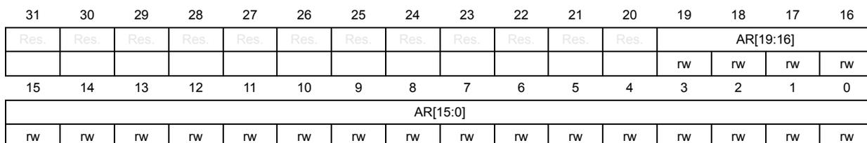
| 31 | 30 | 29 | 28 | 27 | 26 | 25 | 24 | 23 | 22 | 21 | 20 | 19 | 18 | 17 | 16 |
| Res. | Res. | Res. | Res. | Res. | Res. | Res. | Res. | Res. | Res. | Res. | Res. | AR[19:16] | |||
| rw | rw | rw | rw | ||||||||||||
| 15 | 14 | 13 | 12 | 11 | 10 | 9 | 8 | 7 | 6 | 5 | 4 | 3 | 2 | 1 | 0 |
| AR[15:0] | |||||||||||||||
| rw | rw | rw | rw | rw | rw | rw | rw | rw | rw | rw | rw | rw | rw | rw | rw |
Bits 31:20 Reserved, must be kept at reset value.
Bits 19:0 AR[19:0] : Auto-reload value
This field is set by software.
This field can only be written by software when the counter is disabled (RCC_ASCR.CEN = 0)
CA[19:0] is the counter auto-reload value at which to restart the audio synchronization counter from value 0. It defines the counter period.
12.8.49 RCC audio synchronization capture register (RCC_ASCAR)
Address offset: 0x1D4
Reset value: 0x0000 0000
Access to this register can be protected by GTZC_TZSC SAI1SEC and RCC SPRIV or RCC NSPRIV.
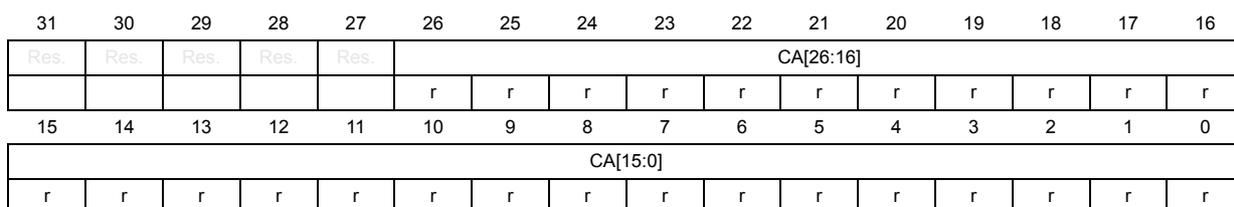
| 31 | 30 | 29 | 28 | 27 | 26 | 25 | 24 | 23 | 22 | 21 | 20 | 19 | 18 | 17 | 16 |
| Res. | Res. | Res. | Res. | Res. | CA[26:16] | ||||||||||
| r | r | r | r | r | r | r | r | r | r | r | |||||
| 15 | 14 | 13 | 12 | 11 | 10 | 9 | 8 | 7 | 6 | 5 | 4 | 3 | 2 | 1 | 0 |
| CA[15:0] | |||||||||||||||
| r | r | r | r | r | r | r | r | r | r | r | r | r | r | r | r |
Bits 31:27 Reserved, must be kept at reset value.
Bits 26:0 CA[26:0] : Capture value
This field is set by hardware.
CA[26:20] is the capture period counter value loaded on the trigger event.
CA[19:0] is the audio synchronization counter value loaded on the trigger event.
12.8.50 RCC audio synchronization compare register (RCC_ASCOR)
Address offset: 0x1D8
Reset value: 0x0000 0000
Access to this register can be protected by GTZC_TZSC_SAI1SEC and RCC_SPRIV or RCC_NSPRIV.
| 31 | 30 | 29 | 28 | 27 | 26 | 25 | 24 | 23 | 22 | 21 | 20 | 19 | 18 | 17 | 16 |
|---|---|---|---|---|---|---|---|---|---|---|---|---|---|---|---|
| Res. | Res. | Res. | Res. | Res. | Res. | Res. | Res. | Res. | Res. | Res. | Res. | CO[19:16] | |||
| rw | rw | rw | rw | ||||||||||||
| 15 | 14 | 13 | 12 | 11 | 10 | 9 | 8 | 7 | 6 | 5 | 4 | 3 | 2 | 1 | 0 |
| CO[15:0] | |||||||||||||||
| rw | rw | rw | rw | rw | rw | rw | rw | rw | rw | rw | rw | rw | rw | rw | rw |
Bits 31:20 Reserved, must be kept at reset value.
Bits 19:0 CO[19:0] : Compare value
This field is set by software.
CO[19:0] is the value to be compared to the audio synchronization counter to generate an compare interrupt event.
12.8.51 RCC clock configuration register 2 (RCC_CFGR4)
Address offset: 0x200
Reset value: 0x0000 0010
Access: word, half-word half-word, and byte access
1 or 2 wait states are inserted only if the access occurs during clock source switch.
Access to this register can be protected by RCC_PRESCSEC and RCC_SPRIV or RCC_NSPRIV.
| 31 | 30 | 29 | 28 | 27 | 26 | 25 | 24 | 23 | 22 | 21 | 20 | 19 | 18 | 17 | 16 |
|---|---|---|---|---|---|---|---|---|---|---|---|---|---|---|---|
| Res. | Res. | Res. | Res. | Res. | Res. | Res. | Res. | Res. | Res. | Res. | Res. | Res. | Res. | Res. | Res. |
| 15 | 14 | 13 | 12 | 11 | 10 | 9 | 8 | 7 | 6 | 5 | 4 | 3 | 2 | 1 | 0 |
| Res. | Res. | Res. | Res. | Res. | Res. | Res. | Res. | Res. | Res. | Res. | HDIV5 | Res. | HPRE5[2:0] | ||
| rw | rw | rw | rw | ||||||||||||
Bits 31:5 Reserved, must be kept at reset value.
Bit 4 HDIV5 : AHB5 for 2.4 GHz RADIO divider when SWS select HSI16 or HSE32
Set and reset by software.
Set to 1 by hardware when entering Stop 1, 2, and 3 mode.
- – When SYSCLK source indicated by SWS is HSI16 or HSE32: HDIV5 is taken into account
- – When SYSCLK source indicated by SWS is PLL1: HDIV5 is taken not taken into account
Caution: Depending on the device voltage range, the software must set this bit correctly to ensure that the AHB5 frequency for the 2.4 GHz RADIO does not exceed the maximum allowed frequency (for more details, refer to Table 109 ). After a write operation to this bit and before decreasing the voltage range, this register must be read to be sure that the new value is taken into account.
0: hclk5 = SYSCLK not divided
1: hclk5 = SYSCLK divided by 2
Bit 3 Reserved, must be kept at reset value.
Bits 2:0 HPRE5[2:0] : AHB5 for the 2.4 GHz RADIO prescaler when SWS select PLL1
Set and cleared by software to control the division factor of the AHB5 clock (hclk5).
Must not be changed when SYSCLK source indicated by SWS is PLL1.
- – When SYSCLK source indicated by SWS is not PLL1: HPRE5 is not taken into account.
- – When SYSCLK source indicated by SWS is PLL1: HPRE5 is taken into account, from the moment the system clock switch occurs
Caution: Depending on the device voltage range, the software must set these bits correctly to ensure that the AHB5 frequency for the 2.4 GHz RADIO does not exceed the maximum allowed frequency (for more details, refer to Table 109: SYSCLK and bus maximum frequency ). After a write operation to these bits and before decreasing the voltage range, this register must be read to be sure that the new value is taken into account.
0xx: hclk5 = SYSCLK not divided
100: hclk5 = SYSCLK divided by 2
101: hclk5 = SYSCLK divided by 3
110: hclk5 = SYSCLK divided by 4
111: hclk5 = SYSCLK divided by 6
12.8.52 RCC RADIO peripheral clock enable register (RCC_RADIOENR)
Address offset: 0x208
Reset value: 0x0000 0000
Access: no wait state; word, half-word half-word, and byte access
Access to this register can be protected by GTZC_TZSC RADIOSEC and RCC SPRIV or NSPRIV.
| 31 | 30 | 29 | 28 | 27 | 26 | 25 | 24 | 23 | 22 | 21 | 20 | 19 | 18 | 17 | 16 |
|---|---|---|---|---|---|---|---|---|---|---|---|---|---|---|---|
| Res. | Res. | Res. | Res. | Res. | Res. | Res. | Res. | Res. | Res. | Res. | Res. | Res. | Res. | RADIO CLKRDY | STRAD IOCLK ON |
| r | rc_w0 | ||||||||||||||
| 15 | 14 | 13 | 12 | 11 | 10 | 9 | 8 | 7 | 6 | 5 | 4 | 3 | 2 | 1 | 0 |
| Res. | Res. | Res. | Res. | Res. | Res. | Res. | Res. | Res. | Res. | Res. | Res. | Res. | Res. | BBCLK EN | Res. |
| rw |
Bits 31:18 Reserved, must be kept at reset value.
Bit 17 RADIOCLKRDY : 2.4 GHz RADIO bus clock ready.
Set and cleared by hardware to indicate that the 2.4 GHz RADIO bus clock is ready and the 2.4 GHz RADIO registers can be accessed.
0: 2.4 GHz RADIO bus clock not ready
1: 2.4 GHz RADIO bus clock ready
Note: Once both RADIOEN and STRADIOCLKON are cleared, RADIOCLKRDY goes low after three hclk5 clock cycles.
Bit 16 STRADIOCLKON : 2.4 GHz RADIO bus clock enable and HSE32 oscillator enable by 2.4 GHz RADIO sleep timer wake-up event
Set by hardware on a 2.4 GHz RADIO sleep timer wake-up event.
Cleared by software writing zero to this bit.
0: 2.4 GHz RADIO bus clock and HSE32 oscillator not requested by 2.4 GHz RADIO sleep timer wake-up event.
1: 2.4 GHz RADIO bus clock and HSE32 oscillator enabled by 2.4 GHz RADIO sleep timer wake-up event
Note: Before accessing the 2.4 GHz RADIO registers the RADIOCLKRDY bit must be checked.
Bits 15:2 Reserved, must be kept at reset value.
Bit 1 BBCLKEN : 2.4 GHz RADIO baseband kernel clock (aclk) enable
Set and cleared by software.
0: 2.4 GHz RADIO baseband kernel clock disabled
1: 2.4 GHz RADIO baseband kernel clock enabled
Note: The HSE32 oscillator needs to be enabled by either HSEON or STRADIOCLKON.
Bit 0 Reserved, must be kept at reset value.
12.8.53 RCC external clock sources calibration register 1(RCC_ECSCR1)
Address offset: 0x210
Power-on reset value: 0x14A0 8000
Reset value not effected by exit Standby mode, nor reset from system reset and BORx (x = 1 to 4).
Access: no wait state; word, half-word half-word, and byte access
Access to this register can be protected by RCC HSESEC and RCC SPRIV or RCC NSPRIV.
| 31 | 30 | 29 | 28 | 27 | 26 | 25 | 24 | 23 | 22 | 21 | 20 | 19 | 18 | 17 | 16 |
|---|---|---|---|---|---|---|---|---|---|---|---|---|---|---|---|
| Res. | HSERDYTRIM[6:0] | HSESFSEN | Res. | HSETRIM[5:0] | |||||||||||
| rw | rw | rw | rw | rw | rw | rw | rw | rw | rw | rw | rw | rw | rw | ||
| 15 | 14 | 13 | 12 | 11 | 10 | 9 | 8 | 7 | 6 | 5 | 4 | 3 | 2 | 1 | 0 |
| XORDYTRIM | HSELD OSEL | Res. | Res. | HSELDOTRIM[3:0] | Res. | Res. | Res. | Res. | Res. | Res. | Res. | Res. | |||
| rw | rw | rw | rw | rw | rw | ||||||||||
Bit 31 Reserved, must be kept at reset value.
Bits 30:24 HSERDYTRIM[6:0] : HSE32 clock ready trimming
HSE clock ready delay value.
HSERDY delay = N * 8 µs. With minimum delay = 160 µs.
Writing values smaller than 0x14 are discarded.
In all cases HSERDY is qualified by hardware XO32 clock ready.
Bit 23 HSESFSEN : HSE32 fast startup enable
0: HSE fast startup disabled.
1: HSE fast startup enabled.
Bit 22 Reserved, must be kept at reset value.
Bits 21:16 HSETRIM[5:0] : HSE32 clock trimming
These bits provide user-programmable capacitor trimming value. It can be programmed to adjust the HSE32 oscillator frequency.
Bit 15 XORDYTRIM : XO32 clock ready trimming
0: XO32 ready after 512 cycles
1: XO32 ready after 1024 cycles
Bit 14 HSELDOSSEL : HSE32 LDO trim selection
0: HSE LDO trim selected from 2.4 GHz RADIO
1: HSE LDO trim selected from HSELDOTRIM
Bits 13:12 Reserved, must be kept at reset value.
Bits 11:8 HSELDOTRIM[3:0] : HSE32 LDO voltage level trimming
This value is only used when HSELDOSSEL = 1.
00: lowest voltage level
01: low mid voltage level
10: high mid voltage level
11: high voltage level
Bits 7:0 Reserved, must be kept at reset value.
12.8.54 RCC LSI key register (RCC_LSIKEYR)
Address offset: 0x220
Reset value: 0x0000 0000
Access: word, half-word half-word, and byte access
Access to this register can be protected by RCC LSISEC and RCC SPRIV or RCC NSPRIV.
| 31 | 30 | 29 | 28 | 27 | 26 | 25 | 24 | 23 | 22 | 21 | 20 | 19 | 18 | 17 | 16 |
|---|---|---|---|---|---|---|---|---|---|---|---|---|---|---|---|
| Res | Res | Res | Res | Res | Res | Res | Res | Res | Res | Res | Res | Res | Res | Res | Res |
| 15 | 14 | 13 | 12 | 11 | 10 | 9 | 8 | 7 | 6 | 5 | 4 | 3 | 2 | 1 | 0 |
| Res. | Res. | Res. | Res. | Res. | Res. | Res. | Res. | KEY[7:0] | |||||||
| rw | rw | rw | rw | rw | rw | rw | rw | ||||||||
Bits 31:8 Reserved, must be kept at reset value.
Bits 7:0 KEY[7:0] : LSI1PREDIV write access enable key
Set and cleared by software to allow write access to LSI1PREDIV even when LSI1 is enabled and ready.
0x4D: write access to LSI1PREDIV granted at all times.
other: write access to LSI1PREDIV disabled when LSI1 is enabled and ready.
12.8.55 RCC register map
Table 117. RCC register map and reset values
| Offset | Register | 31 | 30 | 29 | 28 | 27 | 26 | 25 | 24 | 23 | 22 | 21 | 20 | 19 | 18 | 17 | 16 | 15 | 14 | 13 | 12 | 11 | 10 | 9 | 8 | 7 | 6 | 5 | 4 | 3 | 2 | 1 | 0 |
|---|---|---|---|---|---|---|---|---|---|---|---|---|---|---|---|---|---|---|---|---|---|---|---|---|---|---|---|---|---|---|---|---|---|
| 0x000 | RCC_CR | Res. | Res. | Res. | Res. | Res. | Res. | PLL1RDY | PLL1ON | Res. | Res. | Res. | HSEPRE | HSECGSON | Res. | HSEPRDY | HSEON | Res. | Res. | Res. | Res. | Res. | HSIRDY | HSIKERON | HSION | Res. | Res. | Res. | Res. | Res. | Res. | Res. | Res. |
| Reset value | 0 | 0 | 0 | 0 | 0 | 0 | 0 | 0 | 0 | ||||||||||||||||||||||||
| 0x004 to 0x00C | Reserved | Reserved | |||||||||||||||||||||||||||||||
| 0x010 | RCC_ICSCR3 | Res. | Res. | Res. | Res. | Res. | Res. | Res. | Res. | Res. | Res. | Res. | HSITRIM[4:0] | Res. | Res. | Res. | Res. | HSICAL[11:0] | |||||||||||||||
| Reset value | 1 | 0 | 0 | 0 | 0 | X | X | X | X | X | X | X | X | X | X | X | X | ||||||||||||||||
| 0x014 to 0x0018 | Reserved | Reserved | |||||||||||||||||||||||||||||||
| 0x01C | RCC_CFGR1 | Res. | MCOPRE[2:0] | MCOSEL[3:0] | Res. | Res. | Res. | Res. | Res. | Res. | Res. | Res. | Res. | Res. | Res. | Res. | Res. | Res. | Res. | Res. | Res. | Res. | Res. | SWS[1:0] | SW[1:0] | ||||||||
| Reset value | 0 | 0 | 0 | 0 | 0 | 0 | 0 | 0 | 0 | 0 | 0 | ||||||||||||||||||||||
| 0x020 | RCC_CFGR2 | Res. | Res. | Res. | Res. | Res. | Res. | Res. | Res. | Res. | Res. | Res. | Res. | Res. | Res. | Res. | Res. | Res. | Res. | Res. | Res. | PPPRE2[2:0] | Res. | Res. | PPPRE1[2:0] | Res. | Res. | HPRE[2:0] | |||||
| Reset value | 0 | 0 | 0 | 0 | 0 | 0 | 0 | 0 | |||||||||||||||||||||||||
| 0x024 | RCC_CFGR3 | Res. | Res. | Res. | Res. | Res. | Res. | Res. | Res. | Res. | Res. | Res. | Res. | Res. | Res. | Res. | Res. | Res. | Res. | Res. | Res. | Res. | Res. | Res. | Res. | Res. | PPPRE7[2:0] | Res. | Res. | Res. | Res. | ||
| Reset value | 0 | 0 | 0 | ||||||||||||||||||||||||||||||
| 0x028 | RCC_PLL1CFGR | Res. | Res. | Res. | Res. | Res. | Res. | Res. | Res. | Res. | PLL1RCLKPRERDY | PLL1RCLKPRESTEP | PLL1RCLKPRE | Res. | PLL1REN | PLL1QEN | PLL1PEN | Res. | Res. | Res. | Res. | Res. | PLL1M[2:0] | Res. | Res. | Res. | PLL1FRACEN | PLL1RGE[1:0] | PLL1SRC[1:0] | ||||
| Reset value | 0 | 0 | 0 | 0 | 0 | 0 | 0 | 0 | 0 | 0 | 0 | 0 | 0 | ||||||||||||||||||||
| 0x02C to 0x030 | Reserved | Reserved | |||||||||||||||||||||||||||||||
| 0x034 | RCC_PLL1DIVR | Res. | PLL1R[6:0] | Res. | PLL1Q[6:0] | PLL1P[6:0] | PLL1N[8:0] | ||||||||||||||||||||||||||
| Reset value | 0 | 0 | 1 | 0 | 0 | 0 | 1 | 0 | 0 | 0 | 0 | 0 | 0 | 1 | 0 | 0 | 0 | 0 | 0 | 0 | 0 | 0 | 0 | 0 | 0 | 0 | 0 | 0 | 0 | ||||
| 0x038 | RCC_PLL1FRACR | Res. | Res. | Res. | Res. | Res. | Res. | Res. | Res. | Res. | Res. | Res. | Res. | Res. | Res. | Res. | Res. | PLL1FRACN[12:0] | Res. | Res. | Res. | ||||||||||||
| Reset value | 0 | 0 | 0 | 0 | 0 | 0 | 0 | 0 | 0 | 0 | 0 | 0 | 0 | 0 | 0 | ||||||||||||||||||
| 0x03C to 0x04C | Reserved | Reserved | |||||||||||||||||||||||||||||||
Table 117. RCC register map and reset values (continued)
| Offset | Register | 31 | 30 | 29 | 28 | 27 | 26 | 25 | 24 | 23 | 22 | 21 | 20 | 19 | 18 | 17 | 16 | 15 | 14 | 13 | 12 | 11 | 10 | 9 | 8 | 7 | 6 | 5 | 4 | 3 | 2 | 1 | 0 | |
|---|---|---|---|---|---|---|---|---|---|---|---|---|---|---|---|---|---|---|---|---|---|---|---|---|---|---|---|---|---|---|---|---|---|---|
| 0x050 | RCC_CIER | Res | Res | Res | Res | Res | Res | Res | Res | Res | Res | Res | Res | Res | Res | Res | LSI2RDYIE | Res | Res | Res | Res | Res | Res | Res | Res | Res | Res | PLL1RDYIE | Res | HSERDYE | HSIRDYE | Res | LSERDYE | LSI1RDYIE |
| Reset value | 0 | 0 | 0 | 0 | 0 | 0 | ||||||||||||||||||||||||||||
| 0x054 | RCC_CIFR | Res | Res | Res | Res | Res | Res | Res | Res | Res | Res | Res | Res | Res | Res | Res | LSI2RDYF | Res | Res | Res | Res | Res | Res | Res | Res | Res | Res | PLL1RDYF | Res | HSERDYF | HSIRDYF | Res | LSERDYF | LSI1RDYF |
| Reset value | 0 | 0 | 0 | 0 | 0 | 0 | ||||||||||||||||||||||||||||
| 0x058 | RCC_CICR | Res | Res | Res | Res | Res | Res | Res | Res | Res | Res | Res | Res | Res | Res | Res | LSI2RDYC | Res | Res | Res | Res | Res | Res | Res | Res | Res | Res | PLL1RDYC | Res | HSERDYC | HSIRDYC | Res | LSERDYC | LSI1RDYC |
| Reset value | 0 | 0 | 0 | 0 | 0 | 0 | ||||||||||||||||||||||||||||
| 0x05C | Reserved | Reserved | ||||||||||||||||||||||||||||||||
| 0x060 | RCC_AHB1RSTR | Res | Res | Res | Res | Res | Res | Res | Res | Res | Res | Res | Res | Res | Res | Res | Res | Res | Res | Res | CRORST | Res | Res | Res | Res | Res | Res | Res | Res | Res | Res | Res | LPDMA1RST | |
| Reset value | 0 | 0 | ||||||||||||||||||||||||||||||||
| 0x064 | RCC_AHB2RSTR | Res | Res | XSP1RST | Res | Res | Res | Res | Res | OTFDEC1RST | Res | PKARST | Res | RNGRST | HASHRST | AESRST | Res | Res | Res | Res | Res | Res | Res | Res | Res | Res | GPIOHRST | Res | Res | Res | Res | GPIOCRST | GPIOBRST | |
| Reset value | 0 | 0 | 0 | 0 | 0 | 0 | 0 | 0 | 0 | |||||||||||||||||||||||||
| 0x068 | Reserved | Reserved | ||||||||||||||||||||||||||||||||
| 0x06C | RCC_AHB4RSTR | Res | Res | Res | Res | Res | Res | Res | Res | Res | Res | Res | Res | Res | Res | Res | Res | Res | Res | Res | Res | Res | Res | Res | Res | Res | Res | ADC4RST | Res | Res | Res | Res | Res | |
| Reset value | 0 | |||||||||||||||||||||||||||||||||
| 0x070 | RCC_AHB5RSTR | Res | Res | Res | Res | Res | Res | Res | Res | Res | Res | Res | Res | Res | Res | Res | Res | Res | Res | Res | Res | Res | Res | Res | Res | Res | Res | Res | Res | Res | Res | PTACONVRST | RADIOIRST | |
| Reset value | 0 | 0 | ||||||||||||||||||||||||||||||||
| 0x074 | RCC_APB1RSTR1 | Res | Res | Res | Res | Res | Res | Res | Res | Res | Res | I2C1RST | Res | Res | Res | Res | Res | Res | Res | Res | Res | Res | Res | Res | Res | Res | Res | Res | Res | Res | Res | Res | TIM2RST | |
| Reset value | 0 | 0 | ||||||||||||||||||||||||||||||||
| 0x078 | RCC_APB1RSTR2 | Res | Res | Res | Res | Res | Res | Res | Res | Res | Res | Res | Res | Res | Res | Res | Res | Res | Res | Res | Res | Res | Res | Res | Res | Res | Res | Res | LPTIM2RST | Res | Res | Res | Res | |
| Reset value | 0 | |||||||||||||||||||||||||||||||||
Table 117. RCC register map and reset values (continued)
| Offset | Register | 31 | 30 | 29 | 28 | 27 | 26 | 25 | 24 | 23 | 22 | 21 | 20 | 19 | 18 | 17 | 16 | 15 | 14 | 13 | 12 | 11 | 10 | 9 | 8 | 7 | 6 | 5 | 4 | 3 | 2 | 1 | 0 | |
|---|---|---|---|---|---|---|---|---|---|---|---|---|---|---|---|---|---|---|---|---|---|---|---|---|---|---|---|---|---|---|---|---|---|---|
| 0x07C | RCC_APB2RSTR | Res. | Res. | Res. | Res. | Res. | Res. | Res. | USBRST | Res. | Res. | SAHRST | Res. | Res. | TIM17RST | TIM16RST | Res. | Res. | USART1RST | Res. | Res. | Res. | Res. | Res. | Res. | Res. | Res. | Res. | Res. | Res. | Res. | Res. | Res. | |
| Reset value | 0 | 0 | 0 | 0 | 0 | |||||||||||||||||||||||||||||
| 0x080 | RCC_APB7RSTR | Res. | Res. | Res. | Res. | Res. | Res. | Res. | Res. | Res. | Res. | Res. | Res. | Res. | Res. | Res. | Res. | Res. | Res. | Res. | Res. | LPTIM1RST | Res. | Res. | Res. | I2C3RST | LPUART1RST | SPI3RST | Res. | Res. | Res. | Res. | SYSCFGRST | |
| Reset value | 0 | 0 | 0 | 0 | 0 | |||||||||||||||||||||||||||||
| 0x084 | Reserved | Reserved | ||||||||||||||||||||||||||||||||
| 0x088 | RCC_AHB1ENR | SRAM1EN | Res. | Res. | Res. | Res. | Res. | Res. | GTZC1EN | Res. | Res. | Res. | Res. | Res. | RAMCFGEN | Res. | Res. | Res. | Res. | Res. | CRCEN | Res. | Res. | Res. | FLASHEN | Res. | Res. | Res. | Res. | Res. | Res. | Res. | LPDMA1EN | |
| Reset value | 1 | 0 | 0 | 0 | 1 | 0 | ||||||||||||||||||||||||||||
| 0x08C | RCC_AHB2ENR | Res. | SRAM2EN | XSPI1EN | Res. | Res. | Res. | Res. | OTFDEC1EN | Res. | Res. | PKAEN | Res. | Res. | RNGEN | HASHEN | AESEN | Res. | Res. | Res. | Res. | Res. | Res. | Res. | Res. | GPIOHEN | Res. | Res. | Res. | Res. | Res. | GPIOCEN | GPIOBEN | GPIOAEN |
| Reset value | 0 | 0 | 0 | 0 | 0 | 0 | 0 | 0 | 0 | 0 | 0 | |||||||||||||||||||||||
| 0x090 | Reserved | Reserved | ||||||||||||||||||||||||||||||||
| 0x094 | RCC_AHB4ENR | Res. | Res. | Res. | Res. | Res. | Res. | Res. | Res. | Res. | Res. | Res. | Res. | Res. | Res. | Res. | Res. | Res. | Res. | Res. | Res. | Res. | Res. | Res. | Res. | Res. | ADC4EN | Res. | Res. | Res. | Res. | PWREN | Res. | |
| Reset value | 0 | 0 | ||||||||||||||||||||||||||||||||
| 0x098 | RCC_AHB5ENR | Res. | Res. | Res. | Res. | Res. | Res. | Res. | Res. | Res. | Res. | Res. | Res. | Res. | Res. | Res. | Res. | Res. | Res. | Res. | Res. | Res. | Res. | Res. | Res. | Res. | Res. | Res. | Res. | Res. | Res. | PTACONVEN | RADIOEN | |
| Reset value | 0 | 0 | ||||||||||||||||||||||||||||||||
| 0x09C | RCC_APB1ENR1 | Res. | Res. | Res. | Res. | Res. | Res. | Res. | Res. | Res. | Res. | I2C1EN | Res. | Res. | Res. | Res. | Res. | Res. | Res. | Res. | Res. | Res. | Res. | Res. | Res. | Res. | Res. | Res. | Res. | Res. | Res. | Res. | TIM2EN | |
| Reset value | 0 | 0 | ||||||||||||||||||||||||||||||||
| 0x0A0 | RCC_APB1ENR2 | Res. | Res. | Res. | Res. | Res. | Res. | Res. | Res. | Res. | Res. | Res. | Res. | Res. | Res. | Res. | Res. | Res. | Res. | Res. | Res. | Res. | Res. | Res. | Res. | Res. | Res. | LPTIM2EN | Res. | Res. | Res. | Res. | Res. | |
| Reset value | 0 | |||||||||||||||||||||||||||||||||
| 0x0A4 | RCC_APB2ENR | Res. | Res. | Res. | Res. | Res. | Res. | Res. | USBEN | Res. | Res. | SAI1EN | Res. | Res. | TIM17EN | TIM16EN | Res. | Res. | USART1EN | Res. | Res. | Res. | Res. | Res. | Res. | Res. | Res. | Res. | Res. | Res. | Res. | Res. | Res. | |
| Reset value | 0 | 0 | 0 | 0 | 0 | |||||||||||||||||||||||||||||
| 0x0A8 | RCC_APB7ENR | Res. | Res. | Res. | Res. | Res. | Res. | Res. | Res. | Res. | Res. | RTCAPBEN | Res. | Res. | Res. | Res. | Res. | Res. | Res. | Res. | Res. | LPTIM1EN | Res. | Res. | Res. | I2C3EN | LPUART1EN | SPI3EN | Res. | Res. | Res. | Res. | SYSCFGEN | |
| Reset value | 0 | 0 | 0 | 0 | 0 | 0 | ||||||||||||||||||||||||||||
Table 117. RCC register map and reset values (continued)
| Offset | Register | 31 | 30 | 29 | 28 | 27 | 26 | 25 | 24 | 23 | 22 | 21 | 20 | 19 | 18 | 17 | 16 | 15 | 14 | 13 | 12 | 11 | 10 | 9 | 8 | 7 | 6 | 5 | 4 | 3 | 2 | 1 | 0 | |
|---|---|---|---|---|---|---|---|---|---|---|---|---|---|---|---|---|---|---|---|---|---|---|---|---|---|---|---|---|---|---|---|---|---|---|
| 0x0AC | Reserved | Reserved | ||||||||||||||||||||||||||||||||
| 0x0B0 | RCC_AHB1SMENR | SRAM1SMEN | Res. | ICACHESMEN | Res. | Res. | Res. | Res. | GTZC1SMEN | Res. | Res. | Res. | Res. | Res. | Res. | RAMCFGSMEN | Res. | Res. | Res. | Res. | ORCSMEN | Res. | Res. | Res. | FLASHSMEN | Res. | Res. | Res. | Res. | Res. | Res. | Res. | LPDMA1SMEN | |
| Reset value | 1 | 1 | 1 | 1 | 1 | 1 | 1 | |||||||||||||||||||||||||||
| 0x0B4 | RCC_AHB2SMENR | Res. | SRAM2SMEN | XSPI1SMEN | Res. | Res. | Res. | Res. | OTFDEC1SMEN | Res. | PKASMEN | Res. | Res. | Res. | Res. | RNGSMEN | HASHSMEN | AESSMEN | Res. | Res. | Res. | Res. | Res. | Res. | Res. | GPIOHSMEN | Res. | Res. | Res. | Res. | Res. | GPIOCSMEN | GPIOBSMEN | GPIOASMEN |
| Reset value | 1 | 1 | 1 | 1 | 1 | 1 | 1 | 1 | 1 | 1 | 1 | |||||||||||||||||||||||
| 0x0B8 | Reserved | Reserved | ||||||||||||||||||||||||||||||||
| 0x0BC | RCC_AHB4SMENR | Res. | Res. | Res. | Res. | Res. | Res. | Res. | Res. | Res. | Res. | Res. | Res. | Res. | Res. | Res. | Res. | Res. | Res. | Res. | Res. | Res. | Res. | Res. | Res. | Res. | Res. | ADC4SMEN | Res. | Res. | Res. | PWRSMEN | Res. | |
| Reset value | 1 | 1 | ||||||||||||||||||||||||||||||||
| 0x0C0 | RCC_AHB5SMENR | Res. | Res. | Res. | Res. | Res. | Res. | Res. | Res. | Res. | Res. | Res. | Res. | Res. | Res. | Res. | Res. | Res. | Res. | Res. | Res. | Res. | Res. | Res. | Res. | Res. | Res. | Res. | Res. | Res. | Res. | PTAICONVSMEN | RADIOSMEN | |
| Reset value | 1 | 1 | ||||||||||||||||||||||||||||||||
| 0x0C4 | RCC_APB1SMENR1 | Res. | Res. | Res. | Res. | Res. | Res. | Res. | Res. | Res. | Res. | I2C1SMEN | Res. | Res. | Res. | Res. | Res. | Res. | Res. | Res. | Res. | Res. | Res. | Res. | Res. | Res. | Res. | Res. | Res. | Res. | Res. | Res. | Res. | TIM2SMEN |
| Reset value | 1 | 1 | ||||||||||||||||||||||||||||||||
| 0x0C8 | RCC_APB1SMENR2 | Res. | Res. | Res. | Res. | Res. | Res. | Res. | Res. | Res. | Res. | Res. | Res. | Res. | Res. | Res. | Res. | Res. | Res. | Res. | Res. | Res. | Res. | Res. | Res. | Res. | Res. | Res. | LPTIM2SMEN | Res. | Res. | Res. | Res. | |
| Reset value | 1 | |||||||||||||||||||||||||||||||||
| 0x0CC | RCC_APB2SMENR | Res. | Res. | Res. | Res. | Res. | Res. | Res. | Res. | Res. | Res. | Res. | Res. | Res. | Res. | Res. | Res. | Res. | Res. | Res. | Res. | Res. | Res. | Res. | Res. | Res. | Res. | Res. | Res. | Res. | Res. | Res. | Res. | |
| Reset value | ||||||||||||||||||||||||||||||||||
| 0x0D0 | RCC_APB7SMENR | Res. | Res. | Res. | Res. | Res. | Res. | Res. | Res. | Res. | Res. | Res. | Res. | Res. | Res. | Res. | Res. | Res. | Res. | Res. | Res. | Res. | Res. | Res. | Res. | Res. | Res. | Res. | Res. | Res. | Res. | Res. | Res. | |
| Reset value | ||||||||||||||||||||||||||||||||||
| 0x0D4 to 0x0DC | Reserved | Reserved | ||||||||||||||||||||||||||||||||
Table 117. RCC register map and reset values (continued)
| Offset | Register | 31 | 30 | 29 | 28 | 27 | 26 | 25 | 24 | 23 | 22 | 21 | 20 | 19 | 18 | 17 | 16 | 15 | 14 | 13 | 12 | 11 | 10 | 9 | 8 | 7 | 6 | 5 | 4 | 3 | 2 | 1 | 0 |
|---|---|---|---|---|---|---|---|---|---|---|---|---|---|---|---|---|---|---|---|---|---|---|---|---|---|---|---|---|---|---|---|---|---|
| 0x0E0 | RCC_CCIPR1 | TIM1CSEL | Res. | Res. | Res. | Res. | Res. | Res. | Res. | SYSTICKSEL [1:0] | Res. | Res. | Res. | LPTIM2SEL [1:0] | Res. | Res. | Res. | Res. | Res. | Res. | Res. | I2C1SEL [1:0] | Res. | Res. | Res. | Res. | Res. | Res. | Res. | Res. | Res. | USART1SEL [1:0] | |
| Reset value | 0 | 0 | 0 | 0 | 0 | 0 | 0 | 0 | 0 | ||||||||||||||||||||||||
| 0x0E4 | RCC_CCIPR2 | Res. | ASSEL | Res. | Res. | Res. | Res. | Res. | Res. | Res. | Res. | Res. | Res. | Res. | Res. | Res. | Res. | Res. | Res. | RNGSEL [1:0] | Res. | Res. | Res. | Res. | Res. | SA1SEL [2:0] | Res. | Res. | Res. | Res. | Res. | Res. | |
| Reset value | 0 | 0 | 0 | 0 | 0 | 0 | |||||||||||||||||||||||||||
| 0x0E8 | RCC_CCIPR3 | Res. | Res. | Res. | Res. | Res. | Res. | Res. | Res. | Res. | Res. | Res. | Res. | Res. | Res. | Res. | Res. | Res. | Res. | ADCSEL [2:0] | Res. | LPTIM1SEL [1:0] | Res. | Res. | Res. | I2C3SEL [1:0] | Res. | Res. | SP3SEL [1:0] | Res. | Res. | LPUART1SEL [1:0] | |
| Reset value | 0 | 0 | 0 | 0 | 0 | 0 | 0 | 0 | 0 | 0 | 0 | ||||||||||||||||||||||
| 0x0F0 | RCC_BDCR1 | LSICLK | LSI2RDY | LSI2ON | LSI1PREDIV | LSI1RDY | LSI1ON | LSCOSEL | LSCOEN | LSEGATED | LSIGATED | LSEGATEEN | LSIGATEEN | RADIOI2SEL [1:0] | Res. | BDRST | Res. | LSETRIM [1:0] | Res. | LSEGRDY | LSESYSDRDY | Res. | RTCSEL [1:0] | Res. | Res. | LSESYSEN | LSECSSD | LSECSSON | LSEDRV [1:0] | LSEBYP | LSEDRDY | LSEON | |
| Reset value | 0 | 0 | 0 | 0 | 0 | 0 | 0 | 0 | 0 | 0 | 0 | 0 | 0 | 0 | 0 | 0 | X | X | 0 | 0 | 0 | 0 | 0 | 0 | 0 | 0 | 0 | 1 | 0 | 0 | |||
| 0x0F4 | RCC_CSR | LPWRRSTF | Res. | IWDGRSTF | SFTRSTF | BORRSTF | PINRSTF | OBLRSTF | RMVF | Res. | Res. | Res. | Res. | Res. | Res. | Res. | Res. | Res. | Res. | Res. | Res. | Res. | Res. | Res. | Res. | Res. | Res. | Res. | Res. | Res. | Res. | Res. | Res. |
| Reset value | 0 | 0 | 0 | 1 | 1 | 0 | 0 | ||||||||||||||||||||||||||
| 0x0F8 | RCC_BDCR2 | Res. | Res. | Res. | Res. | Res. | Res. | Res. | Res. | Res. | Res. | Res. | Res. | Res. | Res. | Res. | Res. | Res. | Res. | Res. | Res. | Res. | Res. | Res. | Res. | LSI2CFG[3:0] | Res. | Res. | Res. | Res. | Res. | LSI2MODF[2:0] | |
| Reset value | 0 | 0 | 0 | 0 | 0 | 0 | |||||||||||||||||||||||||||
| 0x0FC to 0x10C | Reserved | Reserved | |||||||||||||||||||||||||||||||
| 0x110 | RCC_SECCFGR | Res. | Res. | Res. | Res. | Res. | Res. | Res. | Res. | Res. | Res. | Res. | Res. | Res. | Res. | Res. | Res. | Res. | Res. | RMVFSEC | Res. | Res. | Res. | Res. | Res. | PLL1SEC | PRESCSEC | SYSCLOCKSEC | LSESEC | LSISEC | Res. | Res. | Res. |
| Reset value | 0 | 0 | 0 | 0 | 0 | 0 | 0 | 0 | |||||||||||||||||||||||||
| 0x114 | RCC_PRIVCFGR | Res. | Res. | Res. | Res. | Res. | Res. | Res. | Res. | Res. | Res. | Res. | Res. | Res. | Res. | Res. | Res. | Res. | Res. | Res. | Res. | Res. | Res. | Res. | Res. | Res. | Res. | Res. | Res. | Res. | Res. | Res. | Res. |
| Reset value | 0 | 0 | |||||||||||||||||||||||||||||||
| 0x118 to 0x1BC | Reserved | Reserved | |||||||||||||||||||||||||||||||
| 0x1C0 | RCC_ASCR | Res. | Res. | Res. | Res. | Res. | Res. | Res. | Res. | TPS[6:0] | Res. | PSC[6:0] | Res. | Res. | Res. | Res. | Res. | Res. | Res. | Res. | CEN | ||||||||||||
| Reset value | 0 | 0 | 0 | 0 | 0 | 0 | 0 | 1 | 0 | 0 | 0 | 0 | 0 | 0 | 0 | ||||||||||||||||||
| 0x1C4 | RCC_ASIER | Res. | Res. | Res. | Res. | Res. | Res. | Res. | Res. | Res. | Res. | Res. | Res. | Res. | Res. | Res. | Res. | Res. | Res. | Res. | Res. | Res. | Res. | Res. | Res. | Res. | Res. | Res. | Res. | Res. | Res. | Res. | Res. |
| Reset value | 0 | 0 | 0 | 0 | |||||||||||||||||||||||||||||
Table 117. RCC register map and reset values (continued)
| Offset | Register | 31 | 30 | 29 | 28 | 27 | 26 | 25 | 24 | 23 | 22 | 21 | 20 | 19 | 18 | 17 | 16 | 15 | 14 | 13 | 12 | 11 | 10 | 9 | 8 | 7 | 6 | 5 | 4 | 3 | 2 | 1 | 0 | |
|---|---|---|---|---|---|---|---|---|---|---|---|---|---|---|---|---|---|---|---|---|---|---|---|---|---|---|---|---|---|---|---|---|---|---|
| 0x1C8 | RCC_ASR | Res. | Res. | Res. | Res. | Res. | Res. | Res. | Res. | Res. | Res. | Res. | Res. | Res. | Res. | Res. | Res. | Res. | Res. | Res. | Res. | Res. | Res. | Res. | Res. | Res. | Res. | Res. | Res. | Res. | ARF | CAEF | COF | CAF |
| Reset value | 0 | 0 | 0 | 0 | ||||||||||||||||||||||||||||||
| 0x1CC | RCC_ASCNTR | Res. | Res. | Res. | Res. | Res. | Res. | Res. | Res. | Res. | Res. | Res. | Res. | CNT[19:0] | ||||||||||||||||||||
| Reset value | 0 | 0 | 0 | 0 | 0 | 0 | 0 | 0 | 0 | 0 | 0 | 0 | 0 | 0 | 0 | 0 | 0 | 0 | 0 | |||||||||||||||
| 0x1D0 | RCC_ASARR | Res. | Res. | Res. | Res. | Res. | Res. | Res. | Res. | Res. | Res. | Res. | Res. | AR[19:0] | ||||||||||||||||||||
| Reset value | 1 | 0 | 0 | 0 | 0 | 0 | 0 | 0 | 0 | 0 | 0 | 0 | 0 | 0 | 0 | 0 | 0 | 0 | 0 | |||||||||||||||
| 0x1D4 | RCC_ASCAR | Res. | Res. | Res. | Res. | Res. | CA[26:0] | |||||||||||||||||||||||||||
| Reset value | 0 | 0 | 0 | 0 | 0 | 0 | 0 | 0 | 0 | 0 | 0 | 0 | 0 | 0 | 0 | 0 | 0 | 0 | 0 | 0 | 0 | 0 | 0 | 0 | 0 | 0 | ||||||||
| 0x1D8 | RCC_ASCOR | Res. | Res. | Res. | Res. | Res. | Res. | Res. | Res. | Res. | Res. | Res. | Res. | CO[19:0] | ||||||||||||||||||||
| Reset value | 0 | 0 | 0 | 0 | 0 | 0 | 0 | 0 | 0 | 0 | 0 | 0 | 0 | 0 | 0 | 0 | 0 | 0 | 0 | |||||||||||||||
| 0x1DC to 0x1FC | Reserved | Reserved | ||||||||||||||||||||||||||||||||
| 0x200 | RCC_CFGR4 | Res. | Res. | Res. | Res. | Res. | Res. | Res. | Res. | Res. | Res. | Res. | Res. | Res. | Res. | Res. | Res. | Res. | Res. | Res. | Res. | Res. | Res. | Res. | Res. | Res. | Res. | Res. | HDIV5 | Res. | HPRE5[2:0] | |||
| Reset value | 1 | 0 | 0 | 0 | ||||||||||||||||||||||||||||||
| 0x204 | Reserved | Reserved | ||||||||||||||||||||||||||||||||
| 0x208 | RCC_RADIOENR | Res. | Res. | Res. | Res. | Res. | Res. | Res. | Res. | Res. | Res. | Res. | Res. | Res. | Res. | RADIOCKRDY | STRADIOCKLON | Res. | Res. | Res. | Res. | Res. | Res. | Res. | Res. | Res. | Res. | Res. | Res. | Res. | Res. | Res. | BBCLKEN | |
| Reset value | 0 | 0 | 0 | |||||||||||||||||||||||||||||||
| 0x20C | Reserved | Reserved | ||||||||||||||||||||||||||||||||
| 0x210 | RCC_ECSCR1 | Res. | HSERDYTRIM[6:0] | HSEFSEN | Res. | HSETRIM[5:0] | XORDYTRIM | HSELDOSEL | Res. | Res. | HSELDOTRIM[3:0] | Res. | Res. | Res. | Res. | Res. | Res. | |||||||||||||||||
| Reset value | 0 | 0 | 1 | 0 | 1 | 0 | 0 | 1 | 1 | 0 | 0 | 0 | 0 | 0 | 1 | 0 | 0 | 0 | 0 | 0 | ||||||||||||||
| 0x214 to 0x21C | Reserved | Reserved | ||||||||||||||||||||||||||||||||
| 0x220 | RCC_LSIKEYR | Res. | Res. | Res. | Res. | Res. | Res. | Res. | Res. | Res. | Res. | Res. | Res. | Res. | Res. | Res. | Res. | Res. | Res. | Res. | Res. | Res. | Res. | Res. | KEY[7:0] | |||||||||
| Reset value | 0 | 0 | 0 | 0 | ||||||||||||||||||||||||||||||
| 0x224 to 0x3FC | Reserved | Reserved | ||||||||||||||||||||||||||||||||
Refer to Section 2.3.2: Memory map and register boundary addresses for the register boundary addresses.