11. Power control (PWR)
11.1 Introduction
The power controller manages all device power supplies and power modes transitions.
11.2 PWR main features
The power controller (PWR) main features are:
- • Power supplies and supply domains
- – Core domain ( \( V_{\text{CORE}} \) )
- – \( V_{\text{DD}} \) domain
- – Analog domain ( \( V_{\text{DDA}} \) )
- – Supply for the SMPS power stage
- – Supply for the 2.4 GHz RADIO
- – \( V_{\text{DDUSB}} \) domain for USB (available only on STM32WBA25xx)
- • System supply voltage regulation
- – SMPS step-down converter
- – Linear voltage regulator (LDO)
- • Power supply supervision
- – BOR monitor (including power-on reset)
- – PVD monitor
- • Power management
- – Operating modes
- – Voltage scaling control
- – Low-power modes
- • GPIO retention in Standby
- • TrustZone ® security and privileged protection
11.3 PWR pins and internal signals
Table 91. PWR input/output pins
| Pin name | Signal type | Description |
|---|---|---|
| VDD | Supply | Main and backup domain supply |
| VDDUSB (1) | Supply | Independent USB supply |
| VDDA | Supply | Analog peripherals supply |
| VDDRF | Supply | 2.4 GHz RADIO RF supply |
| VDDRFPA | Supply | 2.4 GHz RADIO PA regulator supply |
| VDDANA (2) | Supply | 2.4 GHz RADIO analog supply |
| VDDHPA | Output | 2.4 GHz RADIO PA regulator output |
| VSS | Supply | Ground |
| VSSRF | Supply | 2.4 GHz RADIO ground |
| VDD11 | Input/Output | Logic supply ( \( V_{CORE} \) ) |
| VCAP (2) | Output | Logic supply ( \( V_{CORE} \) ) |
| VDDSMPS | Supply | SMPS supply |
| VSSSMPS | Supply | SMPS ground |
| VLXSMPS | Supply | SMPS output |
1. Available only on STM32WBA25xx devices.
2. Available only on STM32WBA23xx devices.
Table 92. PWR internal input/output signals
| Internal signal name | Signal type | Description |
|---|---|---|
| WKUPx_y (x = 1 to 8, y = 1 to 4) | Input | Wake-up event source selection |
| WKUP interrupt | Output | Global WKUP pin interrupt |
| SLEEP | Output | CPU in Sleep mode, device Sleep mode |
| STOP | Output | CPU in DeepSleep mode, device Stop mode |
Each of the wake-up event WKUPx can be generated from device pins or internal events, selected by WUSELx[1:0] in the PWR_WUCR3 register (x = 1 to 8). A WKUP interrupt is generated only when WKUPx is generated from a device pin. WKUPx generated from internal events are associated with an internal event interrupt.
Table 93. PWR wake-up source selection
| Wake-up event | Internal signal source (x = 1 to 8) | |||
|---|---|---|---|---|
| WKUPx_0 (WUSELx = 00) | WKUPx_1 (WUSELx = 01) | WKUPx_2 (WUSELx = 10) | WKUPx_3 (WUSELx = 11) | |
| WKUP1 | PA0 (1) | PB2 | Reserved | Reserved |
| WKUP2 | Reserved | PC13 | Reserved | Reserved |
| WKUP3 | Reserved | PA1 | PB6 | Reserved |
| WKUP4 | PA2 | Reserved | Reserved | Reserved |
| WKUP5 | Reserved | Reserved | Reserved | Reserved |
| WKUP6 | PA12 | PA5 | Reserved | Secure rtc_alra_trg, rtc_alrb_trg, rtc_wut_trg, or RTC_TS |
| WKUP7 | Reserved | PA6 | Reserved | Nonsecure rtc_alra_trg, rtc_alrb_trg, rtc_wut_trg, or RTC_TS |
| WKUP8 | Reserved | PA7 | PB9 | Any secure or nonsecure tamp_trg |
1. Reserved on STM32WBA25xx devices.
11.4 PWR power supplies and supply domains
Figure 30. Power supply overview
The diagram illustrates the power supply overview for a microcontroller, showing various supply domains and their connections:
- Core domain V110: Contains CPU, PWR, RCC, EXTI, GPIO, peripherals, and 2.4 GHz RADIO wakeup. It is connected to VDD and VSS.
- Core domain V111: Contains Peripherals and 2.4 GHz RADIO BB. It is connected to VDD and VSS.
- Retention domain: Contains SRAM2, SRAM1, and 2.4 GHz RADIO SRAMs. It is connected to VDD and VSS.
- Wakeup domain (VDD): Contains HSI16, PLL, LSI1, LSI2, IWDG, and WKUP. It is connected to VDD and VSS.
- Backup domain: Contains RTC, TAMP, and backup registers. It is connected to VDD and VSS.
- Analog domain: Contains ADC with V REF+ and V REF- . It is connected to VDDA and VSS.
- 2.4 GHz RF PHY domain: Contains 2.4 GHz PHY Standby, FSYN LDO, RFFE LDO, HSE32, Int PA, ADC LDO, VCO LDO, and ANA LDO. It is connected to VDDRPA, VDDRF, VSSRF, VDDHPA, VDDANA, and VSSRF.
Power regulation is provided by SMPS/LDO and REG VDDHPA blocks. External pins include VDDUSB, VDD, VDD11/VCAP, VDDSMPS, VLXSMPS, VSSSMPS, VDDA, and VSS. A note indicates that VSS and VSSRF are connected to package exposed pad. MSV77288V2
Warning: When SMPS devices are used in an LDO application, without inductor between VLXSMPS and VDD11, the pins VDDSMPS and VLXSMPS must be connected to the ground.
11.4.1 External power supplies
The devices require a 1.71 V to 3.6 V \( V_{DD} \) operating voltage supply. Several independent supplies can be provided for specific peripherals. Those supplies must not be provided without a valid operating supply on the \( V_{DD} \) pin:
- •
\(
V_{DD} = 1.71 \text{ V to } 3.6 \text{ V}
\)
\( V_{DD} \) is the external power supply for the I/Os, the internal regulator, and the system analog such as reset, power management, and internal clocks. It is provided externally through the \( V_{DD} \) pins. - •
\(
V_{DDUSB} = 3.0 \text{ V to } 3.6 \text{ V}
\)
(only available on STM32WAB25xx)
\( V_{DDUSB} \) is the independent external power supply for the USB GPIO port PB[9:8] I/Os. When no independent supply is used, \( V_{DDUSB} \) shall be connected to \( V_{DD} \) . - •
\(
V_{DDA} = 1.62 \text{ V to } 3.6 \text{ V}
\)
\( V_{DDA} \) is the external analog power supply for ADC. The \( V_{DDA} \) voltage level is independent from the \( V_{DD} \) voltage, and must preferably be connected to \( V_{DD} \) when the peripherals are not used. - •
\(
V_{DDSMPS} = 1.71 \text{ V to } 3.6 \text{ V}
\)
\( V_{DDSMPS} \) is the external power supply for the SMPS step-down converter. It is provided externally through \( V_{DDSMPS} \) supply pin, and must be connected to the same supply as \( V_{DD} \) pin. - • \( V_{LXSMPS} \) is the switched SMPS step-down converter output .
Note: The SMPS power supply pins are available only on specific package with SMPS step-down converter option.
- •
\(
V_{DD11} / V_{CAP} = 0 \text{ V to } 1.2 \text{ V}
\)
\( V_{CORE} \) is the internal power supply for the digital logic. - •
\(
V_{DDRFP_A} = 0 \text{ V to } 3.6 \text{ V}
\)
(need to be above 1.2 V for 2.4 GHz RADIO operation). This supply must be equal or lower than
\(
V_{DDRF}
\)
.
\( V_{DDRFP_A} \) is the external power supply for the 2.4 GHz RADIO front-end part and PA.- – \( V_{DDRFP_A} \) when connected to \( V_{DD11} \) supports a transmit maximum low output power.
- – \( V_{DDRFP_A} \) when connected to \( V_{DD} \) supports a transmit maximum high output power.
- •
\(
V_{DDANA} = 0 \text{ V to } 3.6 \text{ V}
\)
(need to be above 1.2 V for 2.4 GHz RADIO operation). This supply must be equal or lower than
\(
V_{DDRF}
\)
.
\( V_{DDANA} \) is the external power supply for the 2.4 GHz RADIO part, can be connected to \( V_{DD11} \) when REGPASEL select \( V_{DD11} \) . - •
\(
V_{DDRF} = 1.71 \text{ V to } 3.6 \text{ V}
\)
\( V_{DDRF} \) is the external power supply for the 2.4 GHz RADIO. \( V_{DDRF} \) must always be connected to the supply used for \( V_{DD} \) . - •
\(
V_{DDHPA} = 0.9 \text{ V to } 2.3 \text{ V}
\)
\( V_{DDHPA} \) is the internal power supply for the 2.4 GHz RADIO power amplifier.
11.4.2 Application power supply schemes
The device supports different supply schemes, as shown in Figure 31 . The maximum achievable transmit output power from the 2.4 GHz RADIO internal PA is linked to the supply scheme.
- • In packages supporting an SMPS, a maximum transmit low output power can be reached with the lowest power consumption. In this power scheme \( V_{DDRFP A} \) is connected to \( V_{DD11} \) , and REGVDDHPA is connected to \( V_{DD11} \) selected internally by the REGPASEL register bit.
- • In all other power schemes \( V_{DDRFP A} \) is connected to \( V_{DD} \) , providing maximum output power on transmit.
Figure 31. Application power supply schemes
Packages with SMPS
\( V_{DDRFP A} = V_{DD11} \) (transmit default power)
\( V_{DDRFP A} = V_{DD} \) (transmit high output power)
Packages with SMPS use with LDO only
\( V_{DDRFP A} = V_{DD} \) (transmit high output power)
Packages without SMPS
\( V_{DDRFP A} = V_{DD} \) (transmit high output power)
MSV77289V3
11.4.3 Power-up and power-down power sequences
During power-up and power-down phases, the following power sequence requirements must be respected:
- • When \( V_{DD} \) is below 1 V, other power supplies ( \( V_{DDA} \) , \( V_{DDUSB} \) ) must remain below \( V_{DD} + 300 \) mV.
- • When \( V_{DD} \) is above 1 V, all power supplies are independent.
During the power-down phase, \( V_{DD} \) can temporarily become lower than other supplies only if the energy provided to the MCU remains below 1 mJ. This allows external decoupling capacitors with different time constants to be discharged during the power-down transient phase.
11.4.4 Independent analog peripherals supply
To improve A/D conversion accuracy and 2.4 GHz RADIO performance and to extend the supply flexibility, the analog and 2.4 GHz RADIO peripherals have independent power supplies that can be separately filtered and shielded from noise on the PCB:
- • The analog peripheral voltage supply input is available on a separate \( V_{DDA} \) pin
- • The 2.4 GHz RADIO peripheral voltage supply input is available on a separate \( V_{DDRF} \) , \( V_{DDANA} \) , and \( V_{DDRFPA} \) pin.
The \( V_{DDA} \) supply voltage can be different from \( V_{DD} \) . The \( V_{DDA} \) must be present before enabling the analog peripheral supplied by \( V_{DDA} \) (ADC4).
When a single supply is used, \( V_{DDA} \) can be externally connected to \( V_{DD} \) through the external filtering circuit in order to ensure a low-noise \( V_{DDA} \) voltage.
11.4.5 Independent USB transceiver supply
The USB transceiver is supplied from a separate \( V_{DDUSB} \) supply pin. For USB operation the \( V_{DDUSB} \) range is from 3.0 V to 3.6 V independent from \( V_{DD} \) and other supplies.
After reset, the USB transceiver supplied by \( V_{DDUSB} \) is logically and electrically isolated and therefore is not available. The isolation must be removed before using the USB peripheral by setting the USV bit in the PWR_SVMCR register, once the \( V_{DDUSB} \) supply is present.
There is no dedicated \( V_{DDUSB} \) supply monitor. The application software must ensure that \( V_{DDUSB} \) is supplied at the right level before removing the logical and electrical isolation. Ensuring that \( V_{DDUSB} \) is supplied can be done by a software time delay, or measuring \( V_{DDUSB} \) using an ADC channel.
11.4.6 Independent RADIO peripheral supply
The 2.4 GHz RADIO \( V_{DDRF} \) and \( V_{DDRFPA} \) supply voltages can be different from \( V_{DD} \) . The 2.4 GHz RADIO supplies must be present before enabling the 2.4 GHz RADIO.
When a single supply is used, \( V_{DDRF} \) and \( V_{DDRFPA} \) supplies can be externally connected to \( V_{DD} \) through external filtering circuitry to ensure noise-free supply voltages.
11.4.7 Backup domain
The backup domain contains the RTC, TAMP, backup registers supplied from \( V_{CORE} \) , and the LSE oscillator directly supplied from \( V_{DD} \) pin.
Backup domain access
After a system reset, the backup domain (RCC backup domain control register RCC_BDCR1 , RTC registers, TAMP registers, backup registers) is protected against possible unwanted write accesses. To enable access to the backup domain, proceed as follows:
- 1. Enable the power interface clock by setting the PWREN bits in the RCC AHB4 peripheral clock enable register (RCC_AHB4ENR) .
- 2. Set the DBP bit in the PWR disable backup domain register (PWR_DBPR) to enable access to the backup domain.
11.4.8 Internal regulators
The devices embed two regulators: one LDO and one SMPS in parallel to provide the \( V_{CORE} \) (for digital peripherals, SRAMs and embedded flash memory). Both regulators generate this voltage on VDD11 / VCAP pin. The SMPS is available only on some devices.
Both regulators can provide different voltage scaling ranges (voltage scaling) and can operate in Run and Stop modes.
It is possible to switch from SMPS to LDO and from LDO to SMPS and change voltage scaling range on the fly (when the 2.4 GHz RADIO is not active).
Other internal supplies for the 2.4 GHz RADIO are generated for the dedicated regulator.
11.5 PWR system supply voltage regulation
11.5.1 SMPS and LDO embedded regulators
All devices embed an internal linear voltage regulator (LDO). Some devices additionally embed an internal SMPS step-down converter, which can be selected when the application runs, depending on the application requirements.
The SMPS allows the power consumption to be reduced. Some peripherals can be affected by the noise generated by the SMPS, requiring the application to switch to LDO when running this peripheral, to reach the best performances.
The LDO or SMPS can be used in all voltage scaling ranges, and in all Stop modes and Standby with retention mode.
11.5.2 LDO and SMPS versus reset, voltage scaling, and low-power modes
After BOR0 power-on reset and system reset the LDO regulator is enabled in voltage scaling range 2. Switching to the SMPS regulator provides lower consumption in particular at high \( V_{DD} \) voltage level. It is possible to switch from LDO to SMPS, or from SMPS to LDO in any voltage scaling range, by configuring the REGSEL register bit.
When exiting from Stop or Standby retention modes, the regulator is the same than when entering these low-power modes. When exiting from Standby modes, the LDO regulator is always used to startup. When Standby has been entered from the SMPS regulator, after exiting Standby with the LDO, the regulator is then switched automatically to the SMPS regulator.
When exiting from Stop 0 modes the voltage scaling range is the same as on entering Stop 0 mode. When exiting from Stop 1, Stop 2, Stop 3, and Standby modes the voltage scaling range 2 is used.
When the 2.4 GHz RADIO is active, the regulator and voltage scaling range cannot be changed. Any requested regulator or voltage scaling range change while the 2.4 GHz RADIO is active, is suspended and takes effect only after the 2.4 GHz RADIO and PHY have entered Sleep or DeepSleep mode.
11.5.3 LDO and SMPS fast startup
After BOR0 power-on reset, the LDO regulator starts in high-power mode and in slow-startup mode. The slow-startup feature is selected to limit the inrush current after power-on reset. This increases the wake-up time also when exiting Standby modes.
It is possible to configure fast-startup on the fly and it is applied for the next startup either after a system reset or wake-up from standby modes. The fast-startup is selected by setting the FSTEN bit in the PWR_CR3 register. Fast-startup selection applies to both LDO and SMPS regulators.
11.5.4 Dynamic voltage scaling management
The dynamic voltage scaling is a power management technique that consists in increasing or decreasing the voltage used for the digital peripherals ( \( V_{\text{CORE}} \) ), according to the application performance and power consumption needs.
Dynamic voltage scaling to increase \( V_{\text{CORE}} \) is known as overvolting. It allows the device to improve its performance.
Dynamic voltage scaling to decrease \( V_{\text{CORE}} \) is known as undervolting. It is performed to save power, particularly in devices where the energy comes from a battery and is thus limited.
The regulator operates in the following voltage scaling ranges:
- • Range 1 and range 1.5: high performance
It allows a system clock frequency up to 64 MHz, and is required for any 2.4 GHz RADIO transmit and receive operation.
When the 2.4 GHz RADIO is active the range cannot be changed. Any requested voltage scaling range change while the 2.4 GHz RADIO is active, is suspended and only takes effect after the 2.4 GHz RADIO has entered Sleep or DeepSleep mode.
Range 1.5 is used to run the system up to 64 MHz at lower power consumption.
- • Range 2: low-power
The system clock frequency can be up to 16 MHz. The 2.4 GHz RADIO cannot transmit nor receive.
Voltage scaling is selected through the VOS bit in the PWR_VOSR register.
The sequence to switch the voltage scaling from range 2 to range 1 or range 1.5 is the following:
- 1. Program the VOS to range 1 or range 1.5 in the PWR_VOSR
- 2. Wait until the VOSRDY flag is set in the PWR_VOSR
- 3. Enable the HSE32 oscillator and/or PLL source
- 4. Adjust the number of flash wait states according to the new target SYSCLK frequency using flash LATENCY bitfield in FLASH_ACR.
- 5. Switch SYSCLK to HSE32 or pll1rclk.
The sequence to switch the voltage scaling from range 1 or range 1.5 to range 2 is the following:
- 1. Switch to the SYSCLK frequency \( \leq 16 \) MHz, HSI16 or HSE32 divided by 2.
- 2. Wait for the frequency switch to be ready.
- 3. Adjust the number of wait states according to the new target SYSCLK frequency using flash LATENCY bitfield in FLASH_ACR, and SRAMs WSC bitfield in RAMCFG_MxCR.
- 4. Disable the PLL1
- 5. Program the VOS to range 2 in the PWR_VOSR
- 6. Optionally wait until the ACTVOS in the PWR_SVMSR = VOS in the PWR_VOSR and ACTVOSRDY flag is set in PWR_SVMSR
Note: When switching the voltage scaling, the sequence must be completed (VOS = ACTVOS and ACTVOSRDY = 1) before entering Stop, or Standby modes. When the 2.4 GHz RADIO is active (PWR_RADIOSCR.MODE = active) the system does not enter low-power mode and the CPU can enter DeepSleep independently from VOS, ACTVOS and ACTVOSRDY.
11.5.5 2.4 GHz RADIO PA regulator
The PA regulator REG VDDHPA is used to supply the 2.4 GHz RADIO internal PA with the correct voltage level \( V_{DDHPA} \) for a given transmit output power. This regulator output voltage \( V_{DDHPA} \) is controlled from the 2.4 GHz RADIO link layer software. The \( V_{DDHPA} \) maximum supply level and associated maximum transmit output power is depended on the application supply scheme. See Section 11.4.2: Application power supply schemes .
The application software can control the REG VDDHPA regulator input voltage.
- • Force the input voltage selection of the REG VDDHPA regulator to come from VDDRFPA pin by the REGPASEL register bit.
- – When the REG VDDHPA regulator input voltage is forced to VDDRFPA, the power consumption at low transmit output power is higher.
- • Allow the 1.2 V
\(
V_{DDHPA}
\)
voltage level to be generated directly from the VDD11 supply via the REGPABYPEN register bit. This can be selected only when VDD11 is supplied from the device SMPS. This is only available when the input voltage of the REG VDDHPA regulator is not forced to VDDRFPA.
- – When the SMPS is used, allowing the 1.2 V \( V_{DDHPA} \) voltage level to be generated directly from the VDD11 lowers the power consumption at the transmit output levels using this supply level.
The REG VDDHPA is forced off, discharging the external capacitor, in Stop 2, 3, and all Standby modes.
For more information on the 2.4 GHz RADIO transmit output power and REG VDDHPA regulator control, see Section 9.4.3: Transmit output power .
11.6 PWR power supply supervision
11.6.1 Brownout reset (BOR)
The device has an integrated BOR (brownout reset) circuitry. The BOR is active in all power modes, and cannot be disabled. The BOR reset also generates a system reset on pin NRST.
Five BOR thresholds can be selected through option bytes.
A power-on reset is always generated at the \( V_{BOR0} \) thresholds.
The backup domain supplied by \( V_{DD} \) is reset by the \( V_{BOR0} \) thresholds.
The other \( V_{BORx} \) ( \( x = 1 \) to \( 4 \) ) thresholds keep most of the device under system reset until the supply voltage \( V_{DD} \) reaches the specified \( V_{BORx} \) threshold. When \( V_{DD} \) drops below the selected threshold, a system reset is generated on pin NRST. When \( V_{DD} \) is above the \( V_{BORx} \) upper limit, the system reset on pin NRST is released and the system can start.
For more details on the brownout reset thresholds, refer to the electrical characteristics section in the datasheet.
During Stop 1, 2, 3 and Standby modes, it is possible to set the BOR0 in ultra-low-power (discontinuous) mode to further reduce the current consumption by setting the ULPMEN bit in PWR control register 1 (PWR_CR1) .
Warning: In ultralow-power mode, the supply monitoring is discontinuous and can not detect fast drops in supply, hence it must not be used together with autonomous peripherals using HSI16 as kernel clock.
Figure 32. Brownout reset waveform
- 1. The reset temporization \( t_{RSTTEMPO} \) is present only for the BOR0 lowest threshold ( \( V_{BOR0} \) ).
- 2. The rising edge of the system reset NRST can be driven from the \( V_{BOR0} \) power-on reset or \( V_{BORx} \) ( \( x = 1 \) to \( 4 \) ) rising threshold depending on the \( V_{DD} \) rising slope.
11.6.2 Programmable voltage detector (PVD)
The PVD can be used to monitor the \( V_{DD} \) power supply by comparing it to a threshold selected by the PVDLS[2:0] bits in the PWR supply voltage monitoring control register (PWR_SVMCR) . The PVD is enabled by setting the PVDE bit.
A PVDO flag is available in the PWR supply voltage monitoring status register (PWR_SVMSR) to indicate if \( V_{DD} \) is higher or lower than the PVD threshold. This event is internally connected to the EXTI and can generate an interrupt, if enabled through the EXTI registers (refer to Table 105: PWR interrupt requests ).
The rising/falling edge sensitivity of the EXTI line must be configured according to the PVD output behavior. For example, if the EXTI line is configured to rising edge sensitivity, the interrupt is generated when \( V_{DD} \) drops below the PVD threshold. As an example the service routine can perform emergency shutdown tasks.
The PVD can remain active in Stop modes, and the PVD interrupt can wake up the system from Stop mode. The PVD is not functional in Standby mode.
Figure 33. PVD thresholds
The figure illustrates the relationship between the supply voltage ( \( V_{DD} \) ) and the Programmable Voltage Detector (PVD) output. The top graph shows \( V_{DD} \) rising from a low value to a peak and then falling. A horizontal dashed line represents the \( V_{PVD} \) threshold. The bottom graph shows the PVD output, which is a digital signal. When \( V_{DD} \) rises above the threshold, the PVD output goes high. When \( V_{DD} \) falls below the threshold, the PVD output goes low. The hysteresis is indicated as 100 mV, meaning the output will only change state when \( V_{DD} \) crosses the threshold by at least 100 mV.
11.7 PWR power management
11.7.1 PWR power modes
By default, after a system or a power reset, the microcontroller is in Run mode voltage scaling range 2 and the 2.4 GHz RADIO is in DeepSleep. Several low-power modes are available to save power when the CPU or peripherals do not need to be kept running (for example when waiting for an external event). It is up to the user to select the mode that gives the best compromise between low-power consumption, short startup time, and available wake-up sources.
The device features these low-power modes:
- • Run mode:
The CPU is running.
The power consumption in Run mode can be reduced by one of the following means:- – Slowing down the system clocks and configuring voltage scaling to lower-power range.
- – Gating the clocks to the APB and AHB peripherals when they are unused.
- • Sleep mode:
CPU clock off, all peripherals including Cortex-M33 core, NVIC, and SysTick can run and wake up the CPU when an interrupt or an event occurs. Refer to Section 11.7.5: PWR Sleep mode . - • Stop 0, Stop 1 modes:
The Stop modes achieve the lowest power consumption while retaining the content of registers. The SRAM content can be selected to be retained or not. All clocks in the core domain are stopped (except some autonomous peripheral bus and kernel clocks). The PLL1 and HSE32 crystal oscillators are disabled. The HSI16 RC oscillator is disabled when not activated as autonomous peripheral bus or kernel clock. The LSE or LSI can still run.
Some peripherals are autonomous and can operate in Stop modes by requesting their kernel clock, and also in Stop 0 mode when requesting their bus clock as needed. When a peripheral request its (APB or AHB) bus clock, for example in order to transfer data with LPDMA1, the device transitions from Stop 1 to Stop 0 mode.
The I2C, USART, LPUART, SPI, LPTIM, ADC, RTC, TAMP, IWDG can remain active in Stop modes when the kernel clock is LSE, LSI, or HSI16. The 2.4 GHz RADIO can remain active in Stop 0 mode on its kernel clock HSE32. In Stop 0 mode the autonomous peripheral bus clock can remain active using HSI16.
The brownout reset (BOR) always remains active and the PVD can be kept active in Stop modes. In Stop 1 mode the BOR0 can be configured in ultralow-power mode to further reduce power consumption.
Warning: Ultralow-power mode must not be used together with autonomous peripherals using HSI16 as kernel clock.
In Stop 0 mode, the regulator remains in main regulator mode, allowing a very fast wake-up time but with much higher consumption than Stop 1.
When exiting from Stop mode, the system clock is HSI16 at 16 MHz.
Refer to Section 11.7.6: PWR Stop 0 mode , and Section 11.7.7: PWR Stop 1 mode .
- • Stop 2 mode:
The Stop 2 mode achieves lower power consumption while retaining some peripherals and the system configuration registers content. The SRAM content can be selected to be retained or not. All clocks in the core domain are stopped (except some autonomous peripheral kernel clocks). The PLL and HSE32 crystal oscillators are disabled. The HSI16 RC oscillator is disabled when not activated as autonomous peripheral kernel clock. The LSE or LSI can still run.
Some peripherals are autonomous and can operate in Stop 2 mode by requesting their kernel clock as needed.
The I2C3, LPUART1, SPI3, LPTIM1, RTC, TAMP, IWDG, and 2.4 GHz RADIO sleep timer can remain active in Stop 2 mode when the kernel clock is LSE, LSI, or HSI16.
The brownout reset (BOR) always remains active and the PVD can be kept active in Stop 2 mode. The BOR0 can be configured in ultralow-power mode to further reduce power consumption.
Warning: Ultralow-power mode must not be used together with autonomous peripherals using HSI16 as kernel clock.
When exiting from Stop mode, the system clock is HSI16 at 16 MHz.
Refer to Section 11.7.8: PWR Stop 2 mode .
- • Stop 3 mode:
The Stop 3 mode achieves the lowest power consumption while retaining some peripherals and the system configuration registers content. The SRAM content can be selected to be retained or not. All clocks in the core domain are stopped. The PLL, HSI16 and HSE32 crystal oscillators are disabled. The LSE or LSI can still run, but their digital clock must be gated off.
The IWDG can remain active in Stop 3 mode.
The brownout reset (BOR) always remains active and the PVD can be kept active in Stop 3 mode. The BOR0 can be configured in ultralow-power mode to further reduce power consumption.
When exiting from Stop mode, the system clock is HSI16 at 16 MHz.
- • Standby mode:
The Standby mode is used to achieve the lowest power consumption. The internal regulator is switched off so that the core domain is powered off. The PLL1, the HSI16 RC, and the HSE32 crystal oscillators are also switched off. The LSE or LSI can still run.
The IWDG can remain active in Standby mode.
The BOR always remains active in Standby mode. The BOR can be configured in ultralow-power mode to further reduce power consumption during standby mode.
The state of each I/O during Standby mode can be selected by software: I/O with internal pull-up, internal pull-down or floating.
When entering Standby mode, the register content is lost except for registers in the backup domain \( V_{DD} \) and Standby circuitry.
Optionally, SRAMs can be retained in Standby with retention mode, supplied by the regulator.
Optionally, the RTC and TAMPER can remain active when the kernel clock is LSE or LSI, supplied by the regulator (Standby with retention mode).
Optionally, the 2.4 GHz RADIO sleep timer and configuration in RXTRAM, and sequence SRAM can be retained in Standby with retention mode, supplied by the regulator.
The device exits Standby mode when an NRST pin external reset, an IWDG early interrupt or reset, or a WKUP pin event occurs (configurable rising or falling edge). The device exits Standby retention mode when an RTC event (alarm, periodic wake-up,
timestamp), a TAMP tamper detection, or a 2.4 GHz RADIO sleep timer event occurs. The tamper detection can be raised either due to an external pin or due to an internal failure detection.
The system clock after wake-up is HSI16 16 MHz.
Refer to Section 11.7.8: PWR Stop 2 mode .
The operating modes and transitions are shown in Figure 34 .
The power modes overview is shown in Table 94 .
Figure 34. Operating modes
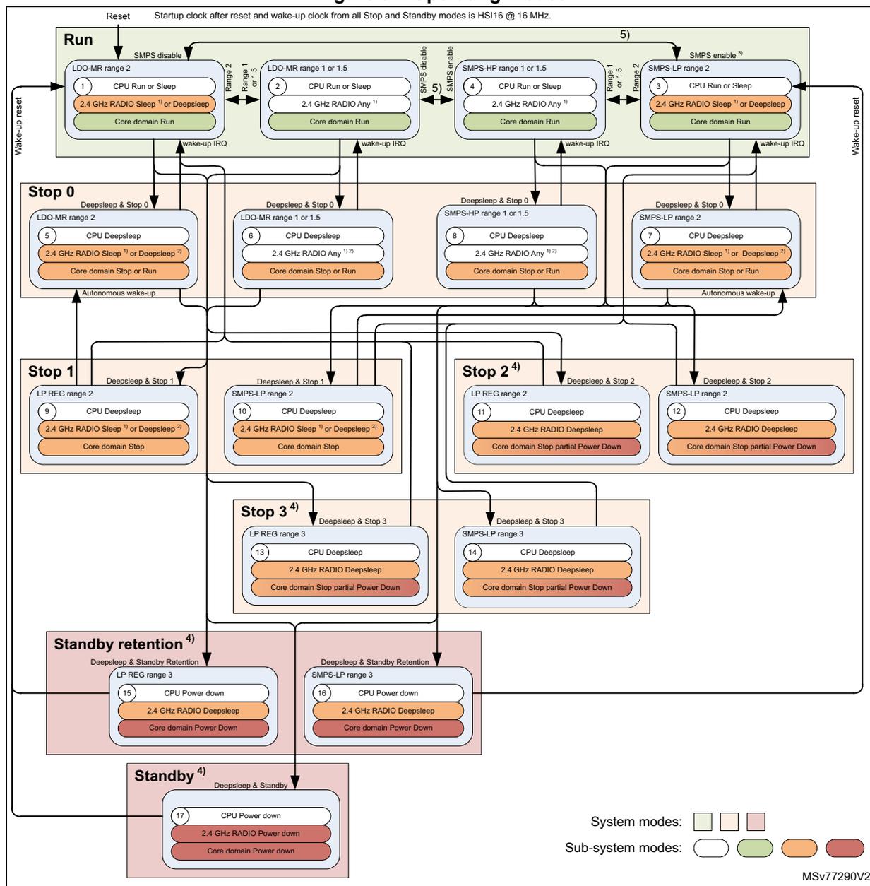
Reset Startup clock after reset and wake-up clock from all Stop and Standby modes is HSI16 @ 16 MHz.
The diagram illustrates the operating modes of the device, categorized into System modes (Run, Stop, Standby) and Sub-system modes (CPU, 2.4 GHz RADIO, Core domain). The modes are organized into a hierarchy starting from Run at the top, branching into Stop 0, Stop 1, Stop 2, Stop 3, Standby retention, and Standby. Each mode box contains the sub-system states for CPU, 2.4 GHz RADIO, and Core domain. Transitions between modes are indicated by arrows, with some transitions requiring specific conditions like 'Deepsleep & Stop 0' or 'Deepsleep & Standby'. Wake-up sources are also indicated, such as 'Wake-up reset', 'wake-up IRQ', and 'Autonomous wake-up'.
System modes:
- Run:
The active mode where the device is powered on and functional. It includes four sub-states based on SMPS/LDO settings:
- LDO-MR range 2 (1): CPU Run or Sleep, 2.4 GHz RADIO Sleep 1) or Deepsleep 1) , Core domain Run
- LDO-MR range 1 or 1.5 (2): CPU Run or Sleep, 2.4 GHz RADIO Any 1) , Core domain Run
- SMPS-HP range 1 or 1.5 (4): CPU Run or Sleep, 2.4 GHz RADIO Any 1) , Core domain Run
- SMPS-LP range 2 (3): CPU Run or Sleep, 2.4 GHz RADIO Sleep 1) or Deepsleep 1) , Core domain Run
- Stop 0:
Low power mode where the CPU is in Deep sleep and the 2.4 GHz RADIO can be in Sleep or Deepsleep. Core domain can be in Stop or Run. It includes four sub-states:
- LDO-MR range 2 (5): CPU Deep sleep, 2.4 GHz RADIO Sleep 1) or Deepsleep 2) , Core domain Stop or Run
- LDO-MR range 1 or 1.5 (6): CPU Deep sleep, 2.4 GHz RADIO Any 1) , Core domain Stop or Run
- SMPS-HP range 1 or 1.5 (8): CPU Deep sleep, 2.4 GHz RADIO Any 1) , Core domain Stop or Run
- SMPS-LP range 2 (7): CPU Deep sleep, 2.4 GHz RADIO Sleep 1) or Deepsleep 2) , Core domain Stop or Run
- Stop 1:
Low power mode where the CPU is in Deep sleep and the 2.4 GHz RADIO is in Sleep or Deepsleep. Core domain is in Stop. It includes two sub-states:
- LP REG range 2 (9): CPU Deep sleep, 2.4 GHz RADIO Sleep 1) or Deepsleep 2) , Core domain Stop
- SMPS-LP range 2 (10): CPU Deep sleep, 2.4 GHz RADIO Sleep 1) or Deepsleep 2) , Core domain Stop
- Stop 2
4)
:
Low power mode where the CPU is in Deep sleep and the 2.4 GHz RADIO is in Deepsleep. Core domain is in Stop partial Power Down. It includes two sub-states:
- LP REG range 2 (11): CPU Deep sleep, 2.4 GHz RADIO Deepsleep, Core domain Stop partial Power Down
- SMPS-LP range 2 (12): CPU Deep sleep, 2.4 GHz RADIO Deepsleep, Core domain Stop partial Power Down
- Stop 3
4)
:
Low power mode where the CPU is in Deep sleep and the 2.4 GHz RADIO is in Deepsleep. Core domain is in Stop partial Power Down. It includes two sub-states:
- LP REG range 3 (13): CPU Deep sleep, 2.4 GHz RADIO Deepsleep, Core domain Stop partial Power Down
- SMPS-LP range 3 (14): CPU Deep sleep, 2.4 GHz RADIO Deepsleep, Core domain Stop partial Power Down
- Standby retention
4)
:
Low power mode where the CPU is in Power down and the 2.4 GHz RADIO is in Deepsleep. Core domain is in Power Down. It includes two sub-states:
- LP REG range 3 (15): CPU Power down, 2.4 GHz RADIO Deepsleep, Core domain Power Down
- SMPS-LP range 3 (16): CPU Power down, 2.4 GHz RADIO Deepsleep, Core domain Power Down
- Standby
4)
:
Low power mode where the CPU is in Power down, the 2.4 GHz RADIO is in Power down, and the Core domain is in Power down. It includes one sub-state:
- (17): CPU Power down, 2.4 GHz RADIO Power down, Core domain Power down
Sub-system modes:
- CPU: Run (green), Deep sleep (light green), Power down (dark green)
- 2.4 GHz RADIO: Sleep (orange), Deepsleep (dark orange), Any (light orange), Power down (dark orange)
- Core domain: Run (green), Stop (light green), Stop partial Power Down (dark green), Power Down (dark green)
MSV77290V2
- Active and Sleep states are controlled by 2.4 GHz RADIO link layer software, independent of the presence of a power supply.
- Only in device Run mode, the 2.4 GHz RADIO operating mode can be changed by software. When the device moves to a low power mode the 2.4 GHz RADIO remains in the same mode.
- For Standby entered from SMPS modes, wake-up is done to Run LDO range 2 mode and a subsequent move to Run SMPS range 2 mode is performed in hardware.
- Stop 2, Stop 3, and Standby mode can only be entered when the 2.4 GHz RADIO is in Deepsleep.
- When the 2.4 GHz radio is active, the SMPS/LDO operating mode cannot be changed. Any request to change the power operating mode is delayed and will take effect only until after the 2.4 GHz RADIO has entered Sleep mode.
Table 94. Low-power mode summary
| Mode name | Entry | Wake-up source (1) | Wake-up system clock | Effect on clocks | Voltage regulator |
|---|---|---|---|---|---|
| Sleep | WFI or Return from ISR | Any interrupt | Same as before entering Sleep mode | CPU clock OFF No effect on other clocks or analog clock sources | Regulator range 1, 1.5, 2 |
| WFE SEVONPEDND = 0 | Wake-up event | ||||
| WFE SEVONPEDND = 1 | Any interrupt, wake-up event | ||||
| Stop 0 | (LPMS = Stop 0 or autonomous peripheral bus clock request active) + SLEEPDEEP bit + WFI or Return from ISR or WFE | Stop 1 wake-up sources + in Stop 0 range 1 or range 1.5: 2.4 GHz RADIO, HSECSS event, USB wake-up. | HSI16 at 16 MHz | All clocks OFF except LSE, LSI and HSI16 or HSE32 when requested as autonomous peripheral kernel or bus clock | |
| Stop 1 | (LPMS = Stop 1 and no autonomous peripheral bus clock request) + SLEEPDEEP bit + WFI or Return from ISR or WFE | Standby with retention wake-up sources + any EXTI line. + autonomous peripherals (reduced peripheral set in Stop 2). | All clocks OFF except LSE, LSI and HSI16 when requested as autonomous peripheral kernel clock. | Regulator range 2 | |
| Stop 2 | (LPMS = Stop 2 and no autonomous peripheral bus clock request and 2.4 GHz RADIO mode = Deep sleep) + SLEEPDEEP bit + WFI or Return from ISR or WFE | ||||
| (LPMS = Stop 3 + (RADIO RSB or RTCRSB = 1) and no autonomous peripheral bus clock request and 2.4 GHz RADIO mode = Deep sleep) + SLEEPDEEP bit + WFI or Return from ISR or WFE | All clocks OFF except LSE and LSI when requested as autonomous peripheral kernel clock, their digital clock must be gated off. | Low voltage | |||
| Stop 3 | (LPMS = Stop 3 + RADIO RSB and RTCRSB = 0 and no autonomous peripheral bus clock request and 2.4 GHz RADIO mode = Deep sleep) + SLEEPDEEP bit + WFI or Return from ISR or WFE | Standby wake-up sources + any EXTI line. | |||
Table 94. Low-power mode summary (continued)
| Mode name | Entry | Wake-up source (1) | Wake-up system clock | Effect on clocks | Voltage regulator |
|---|---|---|---|---|---|
| Standby with retention | (LPMS = Standby + (RADIOUSB or RTCRSB = 1) and no autonomous peripheral bus clock request and 2.4 GHz RADIO mode = Deep sleep) + SLEEPDEEP bit + WFI or Return from ISR or WFE | Standby wake-up sources + RTC event, TAMP event, 2.4 GHz RADIO sleep timer event. | HSI16 at 16 MHz | All clocks OFF except LSI and LSE | Regulator range 2 |
| (LPMS = Standby + (R[2:1]RSB n = 1 and RADIOUSB and RTCRSB = 0) and no autonomous peripheral bus clock request and 2.4 GHz RADIO mode = Deep sleep) + SLEEPDEEP bit + WFI or Return from ISR or WFE | Standby wake-up sources + TAMP event. | All clocks OFF except LSE and LSI when requested as autonomous peripheral kernel clock, their digital clock is be gated off | Low voltage | ||
| Standby | (LPMS = Standby + (R[2:1]RSBn, RADIOUSB and RTCRSB = 0) and no autonomous peripheral bus clock request and 2.4 GHz RADIO mode = Deep sleep) + SLEEPDEEP bit + WFI or Return from ISR or WFE | IWDG event, WKUP event, NRST external reset, BOR reset | All clocks OFF except LSI and LSE | OFF |
1. Refer to Table 95.
Table 95. Functionalities depending on the working mode (1)| Peripheral | Run/Sleep | Stop 0 | Stop 1 | Stop 2 | Stop 3 | Standby retention | Standby | ||||||||
|---|---|---|---|---|---|---|---|---|---|---|---|---|---|---|---|
| Range 1 or 1.5 | Range 2 | Range 1 or 1.5 | Range 2 | Wake-up capability | - | Wake-up capability | - | Wake-up capability | - | Wake-up capability | - | Wake-up capability | - | Wake-up capability | |
| CPU | A | R | - | R | - | R | - | R | - | - | - | - | - | ||
| ICACHE | A | R | - | R | - | R | - | R | - | - | - | - | - | ||
| Flash memory | O (2) | R | - | R | - | R | - | R | - | R | - | R | - | ||
| SRAM1 | A | O | - | O | - | O | - | O | - | O | - | - | - | ||
| SRAM2 | A | O | Y | O | - | O | - | O | - | O | - | - | - | ||
| RAMCFG | O | O | Y | R | - | R | - | R | - | - | - | - | - | ||
Table 95. Functionalities depending on the working mode (1) (continued)
| Peripheral | Run/Sleep | Stop 0 | Stop 1 | Stop 2 | Stop 3 | Standby retention | Standby | ||||||||
|---|---|---|---|---|---|---|---|---|---|---|---|---|---|---|---|
| Range 1 or 1.5 | Range 2 | Range 1 or 1.5 | Range 2 | Wake-up capability | - | Wake-up capability | - | Wake-up capability | - | Wake-up capability | - | Wake-up capability | - | Wake-up capability | |
| SYSCFG | O | O | - | R | - | R | - | R | - | - | - | - | - | ||
| XSPI1 (3) | O | R | - | R | - | - | - | - | - | - | - | - | - | ||
| DLYBXS1 (3) | O | R | - | R | - | - | - | - | - | - | - | - | - | ||
| OTFDEC1 (3) | O | R | - | R | - | - | - | - | - | - | - | - | - | ||
| Backup registers | A | R | - | R | - | R | - | R | - | R | - | - | - | ||
| 2.4 GHz RADIO | O | R | O | R | Y | R | - | - | - | - | - | - | - | - | - |
| 2.4 GHz RADIO SRAM | O | R | O | R | - | R | - | R | - | R | - | O | - | - | - |
| 2.4 GHz RADIO sleep timer | O | O | O | O | Y | O | Y | O | Y | R | - | O | Y | - | - |
| BOR | A | A | - | Y | A | Y | A | Y | A | Y | A | Y | A | Y | |
| PVD | O | O | - | Y | O | Y | O | Y | O | Y | - | - | - | - | |
| HSI16 clock | O | O (4) | - | O (4) | - | O (4) | - | - | - | - | - | - | - | ||
| HSE32 clock | O | O (5) | - | - | - | - | - | - | - | - | - | - | - | ||
| LSI clock | O | O | - | O | - | O | - | O (6) | - | O | - | O | - | ||
| LSE clock | O | O | - | O | - | O | - | O (6) | - | O | - | O | - | ||
| CSSHSE clock security | O | O | - | - | Y | - | - | - | - | - | - | - | - | - | - |
| CSSLSE clock security | O | O | - | Y | O | Y | O | Y | O | Y | O | Y | - | - | |
| RTC | O | O | - | Y | O | Y | O | Y | R (7) | O | Y | - | - | ||
| TAMP | O | O | - | Y | O | Y | O | Y | R (7) | O | Y | - | - | ||
| GPIO | O | R (8) | Y (9) | R (8) | Y (9) | R (8)(10) | Y (9) | R (8)(10) | Y (9) | R (11) | Y (12) | R (11) | Y (12) | ||
| IWDG | O | O | - | Y | O | Y | O | Y | O | Y | O | Y | O | Y | |
| LPDMA1 | O | O | - | Y | R | - | - | - | - | - | - | - | - | - | |
| USART1 | O | O | - | Y | O | Y | - | - | - | - | - | - | - | - | |
| LPUART1 | O | O | - | Y | O | Y | O | Y | R | - | - | - | - | - | |
| I2C1 | O | O | - | Y | O | Y | - | - | - | - | - | - | - | - | |
| I2C3 | O | O | - | Y | O | Y | O | Y | R | - | - | - | - | - | |
| SPI3 | O | O | - | Y | O | Y | O | Y | R | - | - | - | - | - | |
| USB (3) | O | R | O | R | Y | R | - | - | - | - | - | - | - | - | - |
| Peripheral | Run/Sl eep | Stop 0 | Stop 1 | Stop 2 | Stop 3 | Standby retention | Standby | |||||||||
|---|---|---|---|---|---|---|---|---|---|---|---|---|---|---|---|---|
| Range 1 or 1.5 | Range 2 | Range 1 or 1.5 | Range 2 | Wake-up capability | - | Wake-up capability | - | Wake-up capability | - | Wake-up capability | - | Wake-up capability | - | Wake-up capability | ||
| ADC4 | O | O | Y | O | Y | - | - | - | - | - | - | - | - | |||
| Temperature sensor | O | O (13) | Y (13) | O (13) | Y (13) | - | - | - | - | - | - | - | - | |||
| LPTIM1 | O | O | Y | O | Y | O | Y | R | - | - | - | - | - | |||
| LPTIM2 | O | O | Y | O | Y | - | - | - | - | - | - | - | - | |||
| PTACONV | O | R | - | R | - | _(10) | - | _(10) | - | - | - | - | - | |||
| TIMx (x = 2, 16, 17) | O | R | - | R | - | - | - | - | - | - | - | - | - | |||
| SAI1 | O | R | - | R | - | - | - | - | - | - | - | - | - | |||
| RNG | O | R | - | R | - | - | - | - | - | - | - | - | - | |||
| AES | O | R | - | R | - | - | - | - | - | - | - | - | - | |||
| HASH | O | R | - | R | - | - | - | - | - | - | - | - | - | |||
| PKA | O | R | - | R | - | - | - | - | - | - | - | - | - | |||
| CRC | O | R | - | R | - | - | - | - | - | - | - | - | - | |||
| GTZC1_TZSC-(MPCWM1) (3) | O | R | - | R | - | R | - | R | - | - | - | - | - | |||
| GTZC1_TZIC | O | R | - | R | - | R | - | R | - | - | - | - | - | |||
| GTZC1_MPCBB1 | O | R | - | R | - | R | - | R | - | - | - | - | - | |||
| GTZC1_MPCBB2 | O | R | - | R | - | R | - | R | - | - | - | - | - | |||
| SysTick timer | O | R | - | R | - | - | - | - | - | - | - | - | - | |||
| Debug | O | O (14) | - | O (14) | - | O (14) | - | O (14) | - | O (15) | - | O (15) | - | |||
1. A = Active, Y = yes. O = optional (can be enabled/disabled by software). R = Retained, - = not available. Gray cells highlight the wake-up capability in each mode.
2. The flash memory can be configured in power-down mode.
3. Only available on STM32WBA25xx devices.
4. Some peripherals with autonomous mode and wake-up from Stop capability can request HS116 to be enabled. In this case, the oscillator is woken up by the peripheral, and is automatically put off when no peripheral needs it.
5. For the autonomous 2.4 GHz RADIO the HSE32 can be kept running.
6. Digital domain clock must be gated off.
7. RTC and TAMP counting needs to be reinitialized by software after Stop 3 mode exit.
8. GPIO pins from peripherals supporting autonomous mode are still operational.
9. Only GPIOs with enabled wake-up functionality in the EXTI or WKUP are able to wake up the system.
10. GPIO level retention from PTA interface in Stop 2 and Stop 3 mode can be enabled.
11. GPIO level retention in Standby modes can be enabled.
- 12. Only GPIOs with WKUP functionality are able to wake up the system.
- 13. Functional through ADC4 in autonomous mode.
- 14. DBGMCU remains accessible through AP0.
- 15. DBGMCU remains accessible through AP0 when CDBGPWURUPREQ is set.
Debug mode
By default, the debug connection is lost if the application puts the MCU in Stop and Standby modes while the debug features are used. This is due to the fact that the Cortex-M33 core is no longer clocked or powered.
However, by setting some configuration bits in the DBGMCU control registers, the software can be debugged even when using the low-power modes extensively. For more details, refer to Section 41.2.5: DBG low-power modes .
11.7.2 PWR background autonomous mode (BAM)
The devices support a background autonomous mode (BAM), that allows autonomous peripherals to be functional on its bus and kernel clock in Stop 0 mode and on its kernel clock in Stop 0 and Stop 1, and for a limited set of peripherals in Stop 2 modes (when the CPU is in DeepSleep, not running any software). Whenever an autonomous peripheral requests its bus clock, the Stop 0 mode is entered while the CPU remains in DeepSleep.
Stop 0 and Stop 1 modes
In Stop 0 and Stop 1 modes, the autonomous peripherals are ADC, LPTIM, USART, LPUART, SPI, I2C, 2.4 GHz RADIO sleep timer:
- • Peripherals are autonomous only with LSE, LSI or HSI16 used as kernel clock, or HSI16 used as bus clock
- • When an autonomous peripheral requests its bus clock Stop 0 mode is entered while keeping the CPU in DeepSleep.
In Stop 0 mode voltage scaling range 1 and 1.5 the 2.4 GHz RADIO can operate autonomously on HSI16 used as bus clock and HSE32 used as kernel clock. The 2.4 GHz RADIO cannot be autonomous in other Stop modes.
When requesting to enter low-power modes Stop and Standby from Run and an autonomous peripheral bus clock request is active, Stop 0 mode is entered, regardless of the low-power mode selection in LPMS bits. Entering in the LPMS selected low-power mode (Stop 1, 2, 3 and Standby) is delayed until the autonomous peripheral bus clock request is released.
When in Stop 1 mode and an autonomous peripheral requests its bus clock, the Stop 0 mode is entered.
When in Stop 0 mode and all autonomous peripheral bus clock request are deactivated, the low-power mode selected in the LPMS bits is entered. Note that Stop 2, Stop 3, and Standby modes can only be entered when the 2.4 GHz RADIO is in DeepSleep.
Note: As soon as the CPU enters DeepSleep, the system enters Stop mode and the BAM operation peripheral bus clock and SYSCLK is switched to HSI16 at 16 MHz. If an autonomous peripheral operation with higher bus clock frequency is needed, the CPU must enter Sleep and keep the system in Run with the configured Run mode SYSCLK clock frequency.
Stop 2 mode
In Stop 2 mode, the autonomous peripherals are LPTIM1, LPUART1, SPI3, I2C3:
- • Peripherals are autonomous only with LSE, LSI, or HSI16 used as kernel clock.
When in Stop 2 mode an autonomous peripheral shall generate an interrupt to wake up the CPU. From Stop 2 mode, autonomous peripheral BAM operation wake up on bus clock and using the LPDMA1 is not supported.
BAM features
BAM is supported by the autonomous peripherals with the following features:
- • Functionality in Stop 0, 1, and 2 mode thanks to the peripheral kernel clock request capability: the peripheral kernel clock is automatically switched on when requested by a peripheral, and automatically switched off when no peripheral requests it. For the peripheral kernel clock to be switched on, both the peripheralEN and peripheralSMEN bits in the RCC registers must be set.
- • DMA transfers are supported in Stop 0 mode, thanks to the peripheral bus clock request capability: the system clock (HSI16) is automatically switched on when requested by a peripheral, and automatically switched off when no peripheral requests it. When the system clock is requested by an autonomous peripheral and both the peripheralEN and peripheralSMEN bits in the RCC registers are set, the system clock is woken up and distributed to all peripherals for which the RCC peripheralEN and peripheralSMEN bits are set. This makes possible DMA transfers between peripherals and SRAMs. The 2.4 GHz RADIO bus clock is requested independently from the RADIOEN and RADIOSMEN.
- • Automatic start of the peripheral thanks to the hardware synchronous or asynchronous triggers (such as I/Os edge detection and low-power timer events)
- • Wake up the CPU from Deep sleep mode through a peripheral interrupt.
The LPDMA1 is fully functional and the linked-list is updated in Stop 0 mode, allowing the different DMA transfers to be linked without any CPU intervention. This can be used to chain transfers between different peripherals, or to write peripheral registers, in order to change their configuration while in Stop 0 mode.
The DMA transfers from memory to memory can be started by hardware synchronous or asynchronous triggers, and the DMA transfers between peripherals and memories can also be gated by those triggers. In BAM mode only SRAM transfers are supported, flash memory transfers are not supported.
Here below some use-cases that can be done while remaining in Stop 0, 1, and 2 modes:
- • A/D conversion triggered by a low-power timer (or any other trigger)
- – Wake up from Stop mode on analog watchdog if the A/D conversion result is out of the programmed thresholds
- – Wake up from Stop mode on DMA buffer event
- • I
2
C target reception or transmission, SPI reception, UART/LPUART reception
- – Wake up at the end of peripheral transfer or on DMA buffer event
- • I
2
C controller transfer, SPI transmission, UART/LPUART transmission, triggered by a low-power timer (or any other trigger)
- – Example: sensor periodic read
- – Wake up at the end of peripheral transfer or on DMA buffer event
- • Bridges between peripherals
- – Example: A/D converted data transferred by communication peripherals
- • Data transfer from/to GPIO to/from SRAM for:
- – Controlling external components
- – Implementing data transmission and reception protocols
- • Data transfer from one SRAM to another one.
Here below a 2.4 GHz RADIO use-case that can be done while remaining in Stop 0 mode voltage scaling range 1 or range 1.5:
- • Transmit and receive data packets.
- – Wake up at the end of the scheduled event.
11.7.3 PWR Run mode
Slowing down system clocks
In Run mode, the speed of the system clocks (SYSCLK, hclk, pclk) can be reduced by programming the prescaler registers. These prescalers can also be used to slow down the peripherals before entering the Sleep mode.
For more details, refer to Section 12: Reset and clock control (RCC) .
In addition to slowing down the system clocks the voltage scaling range can be changed. When the system clock frequency is low enough, range 2 can be entered.
Peripheral clock gating
In Run mode, the hclk and pclk for individual peripherals and memories can be stopped at any time to reduce the power consumption. The peripheral clock gating is controlled by the RCC_AHBxENR and RCC_APBxENR registers.
In Sleep and Stop 0, 1, and 2 modes, the hclk and pclk for individual peripherals and memories can be stopped automatically. The Sleep and Stop 0, 1, and 2 mode peripheral clock gating is controlled by the RCC_AHBxSMENR and RCC_APBxSMENR registers. For autonomous peripherals to be able to request their clocks the peripheral bus clock in Sleep and Stop 0, 1, and 2 mode must be enabled. Except for the 2.4 GHz RADIO, which requests its bus clock independently from the settings in the RADIOEN and RADIOSMEN register bits.
For the 2.4 GHz RADIO the bus clock is running only in Sleep and Stop 0, 1, and 2 modes when the STRADIOCLKON is set, or when the 2.4 GHz RADIO is active and RADIOEN and RADIOSMEN are set.
11.7.4 PWR low-power modes
Entering into a low-power mode
The MCU enters in low-power modes by
- • The CPU executing the WFI (wait for interrupt), or WFE (wait for event) instructions, or when the SLEEPONEXIT bit in the Cortex-M33 system control register is set on Return from ISR.
Entering into a low-power mode through WFI or WFE is executed only if no interrupt is pending or no event is pending.
Software must enter low-power Stop and Standby modes only when voltage scaling is ready (ACTVOSRDY = 1).
When an autonomous peripheral bus clock request is active only Stop 0 is entered, regardless of the low-power mode set in LPMS register bits.
Stop 2, Stop 3, and Standby modes are only entered when the 2.4 GHz RADIO is in DeepSleep mode.
Exiting a low-power mode
The way the CPU exits the Sleep or Stop mode depends on the way the low-power mode was entered:
- • If the WFI instruction or Return from ISR is used to enter the low-power mode, any peripheral interrupt acknowledged by the NVIC can wake up the device.
- • If the WFE instruction is used to enter the low-power mode, the CPU exits the low-power mode as soon as an event occurs. The wake-up event can be generated by:
- – An NVIC IRQ interrupt:
When SEVONPEND = 0 in the Cortex-M33 system control register
By enabling an interrupt in the peripheral control register and in the NVIC. When the CPU resumes from WFE, the peripheral interrupt pending bit and the NVIC peripheral IRQ channel pending bit (in the NVIC interrupt clear pending register) must be cleared. Only NVIC interrupts with high enough priority wake up and interrupt the CPU.
When SEVONPEND = 1 in the Cortex-M33 system control register
By enabling an interrupt in the peripheral control register and optionally in the NVIC. When the CPU resumes from WFE, the peripheral interrupt pending bit and when enabled the NVIC peripheral IRQ channel pending bit (in the NVIC interrupt clear pending register) must be cleared. All NVIC interrupts wake up the MCU, even the disabled ones. Only enabled NVIC interrupts with high enough priority wake up and interrupt the CPU. - – An event:
Configuring a EXTI line in event mode. When the CPU resumes from WFE, it is not necessary to clear the EXTI peripheral interrupt pending bit or the NVIC IRQ channel pending bit as the pending bits corresponding to the event line is not set. It can be necessary to clear the interrupt flag in the peripheral.
- – An NVIC IRQ interrupt:
The CPU exits Standby mode through a reset. After waking up from Standby mode, the
program execution restarts in the same way as after a reset (boot pin sampling, option bytes loading, reset vector is fetched).
Caution: When the device is in Stop mode, a peripheral interrupt powers on an internal oscillator. The corresponding NVIC interrupt channel must be enabled to allow the interrupt to wake up the CPU from Stop mode. It is not allowed to disable a peripheral interrupt by disabling only the NVIC channel while keeping the peripheral interrupt enabled, as the device could remain in Stop 0, 1, and 2 mode with clock ON.
The peripherals with autonomous mode feature are able to generate an AHB or APB clock request when the device is in Stop 0, 1, and 2 mode, depending on their internal events. The software must ensure that either DMA transfer or interrupt is served, by configuring properly and in a consistent way the RCC, the autonomous peripherals, the DMA channels, and NVIC. Note that when an autonomous peripheral requests the bus clock in Stop mode, the AHB and APB clocks are distributed to all enabled peripherals on the same AHB or APB bus. Consequently, enabled peripherals, even without autonomous mode capability, are temporarily clocked and can also generate an interrupt during this time. These peripheral interrupts also wake up the device from Stop mode.
11.7.5 PWR Sleep mode
I/O states in Sleep mode
In Sleep mode, all I/O pins keep the same state as in Run mode. In addition I/O pins can be toggled through DMA or other active communication peripherals.
To further reduce the power consumption in Sleep mode, disabling the peripheral clocks in Sleep mode can be performed automatically by resetting the corresponding bit in the RCC_AHBxSMENR and RCC_APBxSMENR registers.
Entering the Sleep mode
The MCU enters the Sleep mode as described in Entering into a low-power mode , when the SLEEPDEEP bit in the Cortex-M33 system control register is cleared (see the table below for details on how to enter the Sleep mode).
Exiting the Sleep mode
The MCU exits the Sleep mode as described in Exiting a low-power mode (see the table below for details on how to exit the Sleep mode).
Table 96. Sleep mode
| Sleep mode | Description |
|---|---|
| Mode entry | WFI (wait for interrupt) or WFE (wait for event) while:
|
Table 96. Sleep mode (continued)
| Sleep mode | Description |
|---|---|
| Mode exit | If WFI or Return from ISR was used for entry If WFE was used for entry and SEVONPEND = 0: If WFE was used for entry and SEVONPEND = 1: |
| Wake-up latency | None |
11.7.6 PWR Stop 0 mode
The Stop mode is based on the Core DeepSleep mode combined with peripheral clock gating. The voltage regulator configuration, as used in Run mode, remains the same in Stop 0 mode. In Stop mode, all clocks in the core domain are stopped. The PLL1, HSI16, and HSE32 oscillators are disabled.
Some peripherals with the BAM capability can switch on HSI16 or HSE32 for transferring data (see Section 11.7.2 for details). BAM capable peripherals using HSE32 require the use of Stop 0 mode voltage scaling range 1 or range 1.5.
To reduce the power consumption in Stop mode, disabling the peripheral clocks can be performed automatically by resetting the corresponding bit in the RCC_AHBxSMENR and RCC_APBxSMENR registers. This bit must be set for the autonomous peripherals requesting clocks in Stop 0, 1, and 2 mode.
All register contents are preserved, SRAMs can fully or partially be retained to further reduce consumption.
I/O states in Stop 0 mode
In the Stop 0 mode, all I/O pins keep the same state as in the Run mode. In addition I/O pins can be toggled through DMA or other BAM communication peripherals.
Entering the Stop 0 mode
The MCU enters the Stop 0 mode as described in Entering into a low-power mode , when the SLEEPDEEP bit in the Cortex-M33 system control register is set. The regulator is kept in the same regulation mode and voltage scaling range as used in Run mode (see the table below for details on how to enter the Stop 0 mode).
If the flash memory programming is ongoing, the Stop 0 mode entry is delayed until the memory access is finished.
If an access to the APB domain is ongoing, the Stop 0 mode entry is delayed until the APB access is finished.
In Stop 0 mode, the following features can be selected by programming the individual control bits:
- • The independent watchdog (IWDG) is started by writing to its key register or by hardware option. Once started, it cannot be stopped except by a reset (see Section 32.4: IWDG functional description ).
- • The real-time clock (RTC) and tamper (TAMP) is configured by the RTCSEL bit in the RCC backup domain control register (RCC_BDCR1) .
- • The internal RC oscillator LSI clock, or LSI clock divided by 128, is configured by the LSI1ON and LSI1PREDIV bits in RCC_BDCR1.
- • The external 32.768 kHz oscillator (LSE) is configured by the LSEON bit in RCC_BDCR1.
- • The 2.4 GHz RADIO sleep timer is configured through the link layer software.
- • The SRAM1 retention is configured by the SRAM1PDS bit in PWR control register 2 (PWR_CR2) .
- • The SRAM2 retention is configured by the SRAM2PDSx bit in PWR control register 2 (PWR_CR2) .
- • The peripheral SRAM retention is configured by PKARAMPDS and PRAMPDS in PWR control register 2 (PWR_CR2) .
In Stop 0 mode voltage scaling range 1 and 1.5, the following features can be selected by programming the individual control bits:
- • In addition to the Stop 0 features above, the 2.4 GHz RADIO configured through the link layer software.
Several peripherals can be autonomous in Stop 0 mode, increasing power consumption if enabled (see Section 11.7.2 for more details).
The PVD can be used in Stop mode. If not needed, it must be disabled by software to reduce power consumption.
The ADC4 and the temperature sensor can consume power during the Stop mode, unless they are disabled before entering this mode.
Entering the Stop 1, 2, 3 and Standby modes from Stop 0
When entering low power with Stop 1, 2, 3 or Standby selected in LPMS and an autonomous peripheral bus clock request is active, Stop 0 mode is entered instead. Only when all autonomous peripheral bus clock requests are deasserted the LPMS selected low-power mode is subsequently entered. Stop 2, Stop 3, and Standby modes are only entered when the 2.4 GHz RADIO is in DeepSleep.
Exiting the Stop 0 mode
The MCU exits the Stop 0 mode as described in Exiting a low-power mode (see Table 97 ).
When exiting Stop 0 mode by issuing an interrupt or a wake-up event, HSI16 is selected as system clock.
Several peripherals are autonomous in Stop mode, and can generate interrupts with wake-up from Stop capability. All peripheral clocks must be enabled to allow a wake-up from Stop interrupt (see Peripheral clock gating ).
When exiting the Stop 0 mode, the MCU is in Run mode with the same voltage scaling range as before entering Stop 0 mode.
The MCU can enter another low-power mode, as selected in LPMS, from the Stop 0 mode when all autonomous peripheral bus clocks requests are deasserted.
Table 97. Stop 0 mode
| Stop 0 mode | Description |
|---|---|
| Mode entry from Run | WFI (wait for interrupt) or WFE (wait for event) while:
On Return from ISR while:
– LPMS = Stop 0 in PWR_CR1 or autonomous peripheral bus clock request is active Note: To enter Stop 0 mode, all EXTI line pending bits (in the EXTI rising edge pending register (EXTI_RPR1) and EXTI falling edge pending register (EXTI_FPR1) ), and the peripheral flags generating wake-up interrupts must be cleared. Otherwise, the Stop 0 mode entry procedure is ignored and the program execution continues. |
| Mode entry from Stop 1 | Autonomous peripheral bus clock request active |
Table 97. Stop 0 mode (continued)
| Stop 0 mode | Description |
|---|---|
| Mode exit to Run | If WFI or Return from ISR was used for entry:
If WFE was used for entry and SEVONPEND = 0:
If WFE was used for entry and SEVONPEND = 1:
Note: All peripheral clocks must be enabled to allow this peripheral to generate a wake-up from Stop interrupt (peripheralEN, and peripheralSMEN bits must be set in the RCC, and a functional independent clock must be selected). |
| Mode exit to low-power modes | All autonomous peripheral bus clock requests deasserted. |
| Wake-up latency | HSI16 wake-up time when applicable and flash wake-up time from Stop 0 mode. |
11.7.7 PWR Stop 1 mode
The Stop 1 mode is similar to the Stop 0 mode in voltage scaling range 2, except that the regulator is in low-power mode (see the table below for details on how to enter and exit Stop 1 mode).
The BOR is always available in Stop 1 mode. When not using BAM operation with HSI16 as kernel clock, the BOR0 can be forced in ultralow-power mode by the ULPMEN bit in the PWR_CR1 to reach the lowest power consumption.
Entering the Stop 1 mode
The MCU enters the Stop 1 mode in the same way as entering Stop 0. Whenever an autonomous peripheral bus clock request is active, Stop 1 mode is not entered and Stop 0 mode is entered instead.
Entering the Stop 0 mode from Stop 1
When in low-power Stop 1 mode, an autonomous peripheral bus clock request is activated. The Stop 0 mode voltage scaling range 2 is entered with HSI16 as system clock and HDIV5 is set to divide-by-2 by hardware.
Exiting the Stop 1 mode
The MCU exits the Stop 1 mode as described in Exiting a low-power mode (see Table 98 ).
When exiting Stop 1 mode by issuing an interrupt or a wake-up event, Run voltage scaling range 2 with HSI16 is selected as the system clock, and HDIV5 is set to divide-by-2 by hardware. Before entering Stop 1 mode, the software must configure adequate FLASH wait states latency to at least 1 in FLASH_ACR register and SRAMs wait states to at least 1 in RAMCFG_MxCR.
Table 98. Stop 1 mode
| Stop 1 mode | Description |
|---|---|
| Mode entry | WFI (wait for interrupt) or WFE (wait for event) while:
On Return from ISR while:
– LPMS = Stop 1 in PWR_CR1 and all autonomous peripheral bus clock requests deactivated. – LPMS = Stop 2 in PWR_CR1 and 2.4 GHz RADIO not in Deep sleep. – LPMS = Stop 3 in PWR_CR1 and 2.4 GHz RADIO not in Deep sleep. – LPMS = Standby in PWR_CR1 and all autonomous peripheral bus clock requests deactivated and 2.4 GHz RADIO not in Deep sleep. Note: To enter Stop 1 mode, all EXTI line pending bits (in EXTI rising edge pending register (EXTI_RPR1) and EXTI falling edge pending register (EXTI_FPR1)), and the peripheral flags generating wake-up interrupts must be cleared. Otherwise, the Stop 1 mode entry procedure is ignored and the program execution continues. |
Table 98. Stop 1 mode (continued)
| Stop 1 mode | Description |
|---|---|
| Mode exit to Run | If WFI or Return from ISR was used for entry
If WFE was used for entry and SEVONPEND = 0:
If WFE was used for entry and SEVONPEND = 1:
Any peripheral interrupt occurring when the AHB/APB clocks are present due to an autonomous peripheral clock request (the peripheral vector must be enabled in the NVIC) Note: All peripheral clocks must be enabled to allow this peripheral to generate a wake-up from Stop interrupt (peripheralEN and peripheralSMEN bits must be set in the RCC, and a functional independent clock must be selected). |
| Mode exit to Stop 0 | Autonomous peripheral bus clock request active. |
| Wake-up latency | HSI16 wake-up time and regulator wake-up time from low-power mode + flash wake-up time from Stop 1 mode. |
11.7.8 PWR Stop 2 mode
The Stop 2 mode is similar to the Stop 1 mode except that part of the peripherals is powered down (see the Table 95: Functionalities depending on the working mode for details).
The BOR is always available in Stop 2 mode. When not using autonomous peripheral operation with HSI16 as kernel clock, the BOR0 can be forced in ultralow-power mode by the ULPMEN bit in the PWR_CR1 to reach the lowest power consumption.
I/O states in Stop 2 mode
Before entering Stop 2 mode the peripherals that are not retained shall be disabled and unselected from the GPIO alternate functions. Except for the PTACONV, where the GPIO state can be retained when enabled in the PTASREN register bit, the GPIO retains the output level. When entering Stop 2 mode, PTACONV signals enabled for Stop 2 mode retention keep their state during and after exiting from Stop 2 mode until the PTASR bit is cleared by software. When entering Stop 2 mode the PTASR bit is set by hardware when enabled in PTASREN. The PTASR only controls output levels, it does not affect the GPIO
pulls, analog, input and output states. When exiting from Stop 2 and before removing the PTACONV retention, the PTACONV peripheral must be reinitialized. Once the PTACONV peripheral configuration is reconfigured, disable the retention in PTASR.
Entering the Stop 2 mode
The MCU enters the Stop 2 mode in the same way as entering Stop 0. Whenever an autonomous peripheral bus clock request is active, Stop 2 mode is not entered and Stop 0 mode is entered instead.
Stop 2 mode is only entered when the 2.4 GHz RADIO is in DeepSleep mode. Whenever the 2.4 GHz RADIO is in Active or Sleep mode, Stop 0 or Stop 1 mode is entered instead.
Note: Autonomous peripherals in Stop 2 mode should be configured by software to only request a bus clock when also generating a peripheral IRQ event to wake up the CPU.
Exiting the Stop 2 mode
The MCU exits the Stop 2 mode as described in Exiting a low-power mode (see Table 98 ). The STOP2F status flag in the PWR status register (PWR_SR) indicates that the MCU was in Stop 2 mode. The powered down peripherals registers are reset after wake-up from Stop 2.
When exiting Stop 2 mode by issuing an interrupt or a wake-up event, Run range 2 with HSI16 is selected as the system clock and HDIV5 is set to divide-by-2 by hardware. Before entering Stop 2 mode software must configure adequate FLASH wait states latency to at least 1 in FLASH_ACR register and SRAMs wait states to at least 1 in RAMCFG_MxCR.
Table 99. Stop 2 mode
| Stop 2 mode | Description |
|---|---|
| Mode entry | WFI (wait for interrupt) or WFE (wait for event) while:
On Return from ISR while:
– LPMS = Stop 2 in PWR_CR1 and all autonomous peripheral bus clock requests deasserted and 2.4 GHz RADIO in DeepSleep. – LPMS = Stop 3 in PWR_CR1, RADIOUSB or RTCRSB = 1, and all autonomous peripheral bus clock requests de-asserted and 2.4 GHz RADIO in DeepSleep. Note: To enter Stop 2 mode, all EXTI line pending bits (in EXTI rising edge pending register (EXTI_RPR1) and EXTI falling edge pending register (EXTI_FPR1) ), and the peripheral flags generating wake-up interrupts must be cleared. Otherwise, the Stop 2 mode entry procedure is ignored and the program execution continues. |
Table 99. Stop 2 mode (continued)
| Stop 2 mode | Description |
|---|---|
| Mode exit to Run | If WFI or Return from ISR was used for entry
If WFE was used for entry and SEVONPEND = 0:
If WFE was used for entry and SEVONPEND = 1:
Note: All peripheral clocks must be enabled to allow this peripheral to generate a wake-up from Stop interrupt (peripheralEN and peripheralSMEN bits must be set in the RCC, and a functional independent clock must be selected). |
| Wake-up latency | HSI16 wake-up time and regulator wake-up time from low-power mode + flash wake-up time from Stop 2 mode. |
11.7.9 PWR Stop 3 mode
The Stop 3 mode is similar to the Stop 2 mode except that there is no wake-up from autonomous peripherals (see the Table 95: Functionalities depending on the working mode for details).
The BOR is always available in Stop 3 mode. The BOR0 can be forced in ultralow-power mode by the ULPMEN bit in the PWR_CR1 to reach the lowest power consumption.
I/O states in Stop 3 mode
Before entering Stop 3 mode the peripherals that are not retained must be disabled and unselected from the GPIO alternate functions. Except for the PTACONV, where the GPIO state can be retained when enabled in the PTASREN register bit, the GPIO retains the output level. When entering Stop 3 mode, PTACONV signals enabled for Stop 3 mode retention keep their state during and after exiting from Stop 3 mode until the PTASR bit is cleared by software. When entering Stop 3 mode the PTASR bit is set by hardware when enabled in PTASREN. The PTASR only controls output levels, it does not affect the GPIO pulls, analog, input and output states. When exiting from Stop 3 and before removing the
PTACONV retention, the PTACONV peripheral must be reinitialized. Once the PTACONV peripheral configuration is reconfigured, disable the retention in PTASR.
Entering the Stop 3 mode
The MCU enters the Stop 3 mode in the same way as entering Stop 0. Whenever an autonomous peripheral bus clock request is active, Stop 3 mode is not entered and Stop 0 mode is entered instead.
When RTCRSB or RADIORSB is 1, Stop 3 mode is not entered and Stop 2 mode is entered instead.
Regardless of an active autonomous peripheral kernel clock request, when entering Stop 3 mode the HSI16 oscillator and all clocks in the \( V_{CORE} \) domain stopped. LSI and LSE clocks in the digital domain shall be gated off by software in the RCC, by LSIGATEEN and LSEGATEEN.
Stop 3 mode is only entered when the 2.4 GHz RADIO is in DeepSleep mode. Whenever the 2.4 GHz RADIO is in Active or Sleep mode, Stop 0 or Stop 1 mode is entered instead.
Exiting the Stop 3 mode
The MCU exits the Stop 3 mode as described in Exiting a low-power mode (see Table 98 ). The STOP2F status flag in the PWR status register (PWR_SR) indicates that the MCU was in Stop 3 mode. The powered down peripherals registers are reset after wake-up from Stop 3.
When exiting Stop 3 mode by issuing an interrupt or a wake-up event, Run voltage scaling range 2 with HSI16 is selected as the system clock and HDIV5 is set to divide-by-2 by hardware. Before entering Stop 3 mode, the software must configure adequate FLASH wait states latency to at least 1 in FLASH_ACR register and SRAMs wait states to at least 1 in RAMCFG_MxCR. The gating of LSI and LSE clocks in the digital domain shall be removed by software in the RCC LSIGATEEN and LSEGATEEN. The RTC and TAMP counting need to be reinitialized by software.
Table 100. Stop 3 mode
| Stop 3 mode | Description |
|---|---|
| Mode entry | WFI (wait for interrupt) or WFE (wait for event) while:
On Return from ISR while:
– LPMS = Stop 3 in PWR_CR1, RTCRSB and RADIORSB are 0, and all autonomous peripheral bus clock requests deasserted and 2.4 GHz RADIO in DeepSleep. Note: To enter Stop 3 mode, all EXTI line pending bits (in EXTI rising edge pending register (EXTI_RPR1) and EXTI falling edge pending register (EXTI_FPR1)), and the peripheral flags generating wake-up interrupts must be cleared. Otherwise, the Stop 3 mode entry procedure is ignored and the program execution continues. |
Table 100. Stop 3 mode (continued)
| Stop 3 mode | Description |
|---|---|
| Mode exit to Run | If WFI or Return from ISR was used for entry
If WFE was used for entry and SEVONPEND = 0:
If WFE was used for entry and SEVONPEND = 1:
|
| Wake-up latency | HSI16 wake-up time and regulator wake-up time from low-power mode + flash wake-up time from Stop 3 mode. |
11.7.10 PWR Standby mode
It is based on the Cortex-M33 DeepSleep mode, with the voltage regulators disabled (except when SRAM1, SRAM2, 2.4 GHz RADIO RAMs and 2.4 GHz RADIO sleep timer are retained). The PLL1, HSI16, and HSE32 oscillators are also switched off.
The register contents are lost except for SRAMs and registers in the retention domain and backup domain \( V_{CORE} \) when enabled and the backup domain \( V_{DD} \) and Standby circuitry (see Figure 30 ). SRAMs' content can be preserved depending on the RxRSBy bits configuration in PWR_CR1. In this case, the regulator is ON and provides the supply to SRAMs.
Also the 2.4 GHz RADIO SRAMs can be retained and the 2.4 GHz RADIO sleep timer kept operational depending on RADIORSB bit configuration in PWR_CR1.
The RTC and TAMP can be retained when enabled in RTCRSB bit in PWR_RC1.
The BOR is always available in Standby mode. The ULPMEN bit in the PWR_CR1 register must be configured to 1 to reach the lowest power consumption by forcing the BOR0 in ultralow-power mode.
I/O states in Standby mode
In the Standby mode, the GPIOs are by default in floating state. If Standby GPIO retention is enabled in the PWR_IORETENRx register, the GPIO retains the pull or output level. When entering Standby mode, GPIOs that are enabled for Standby mode retention keep their pull or level during and after exiting from Standby mode until the PWR_IORETRx bit is cleared by software. When entering Standby mode the PWR_IORETRx bit is set by hardware for the
GPIOs with Standby retention enabled. Only once PWR_IORETRx is cleared by software, the GPIO configuration is switched to that defined below:
- • When GPIO is not selecting an alternate function GPIO configuration is applied
- • When GPIO is selecting an alternate function the selected peripheral alternate function control is applied
The GPIO Standby retention enable information in PWR_IORETENRx and PWR_IORETRx are retained in Standby mode.
Note: The Standby GPIO retention level cannot be guaranteed when the GPIO port pin is connected to a low impedance destination.
Table 101. GPIO retention pin with pull-up and pull-down
| PWR_IORETEN | GPIO port pin configuration before entering Standby | GPIO port pin configuration in Standby |
|---|---|---|
| 0 | Any | High-Z |
| 1 | Input no pulls | High-Z |
| Input or output with pull-up | Pull-up | |
| Input or output with pull-down | Pull-down | |
| Output no pulls driving level high | Pull-up | |
| Output no pulls driving level low | Pull-down |
For GPIO port pins enabled to be functional in Standby modes, the Standby GPIO retention can also be controlled in the PWR_IORETENRx register. The following GPIO functions are available in Standby modes:
- • RTC outputs on PC13 and/or PB2 (standby GPIO retention must be disabled), when retention is enabled with register bit RTCRSB.
- • TAMP tamper pins, when retention enabled with register bit RTCRSB.
- • WKUPx_y wake-up pins
- • LSE pins on PC14 and/or PC15 (Standby GPIO retention must be disabled)
- • JTDO/TRACE SWO on PB3 when debugger is connected and CDBGPWRUPREQ is set (Standby GPIO retention must be disabled)
When waking up from Standby with a system reset (NRST) GPIO retention is removed before the software can reconfigure the GPIO port pins in the GPIO peripheral.
Entering Standby mode
The MCU enters the Standby mode as described in Entering into a low-power mode , when the SLEEPDEEP bit in the Cortex-M33 system control register is set (see Table 102 ).
Whenever an autonomous peripheral bus clock request is active, Standby mode is not entered and Stop 0 mode is entered instead.
Standby mode is only entered when the 2.4 GHz RADIO is in DeepSleep mode. Whenever the 2.4 GHz RADIO is in Active or Sleep mode Stop mode is entered instead.
In Standby mode, the following features can be selected by programming individual control bits:
- • The independent watchdog (IWDG) is started by writing to its key register or by hardware option. Once started it cannot be stopped except by a reset (see Section 32.4: IWDG functional description ).
- • The internal RC oscillator LSI clock or LSI clock divided by 128 is configured by the LSI1ON and LSI1PREDIV bits in RCC_BDCR1.
- • The external 32.768 kHz oscillator (LSE) is configured by the LSEON bit in RCC_BDCR1.
- • The real-time clock (RTC) and tamper (TAMP) is retained by the RTCRSB and is configured by the RTCSEL bit in RCC backup domain control register (RCC_BDCR1) . Available in Standby retention mode.
- • The 2.4 GHz RADIO SRAMs and 2.4 GHz RADIO sleep timer retained by the RADIORSB bit in PWR control register 1 (PWR_CR1) . Available in Standby retention mode.
- • SRAM1 retention configured by the R1RSB bit in PWR control register 1 (PWR_CR1) . Available in Standby retention mode.
- • SRAM2 retention configured by the R2RSBx bit in PWR control register 1 (PWR_CR1) . Available in Standby retention mode.
When RTCRSB or RADIORSB is 1, voltage range 2 is used in Standby retention mode. When RTCRSB and RADIORSB are 0 and at least one RxRSBy is 1, low voltage is used in Standby retention mode.
Exiting Standby mode
The MCU exits the Standby mode as described in Exiting a low-power mode . The SBF status flag in the PWR status register (PWR_SR) indicates that the MCU was in Standby mode (see Table 102 for more details on how to exit Standby mode).
Table 102. Standby mode
| Standby mode | Description |
|---|---|
| Mode entry | WFI (wait for interrupt) or WFE (wait for event) while:
On Return from ISR while:
In Standby retention mode the Vcore level depend on RTCRSB and RADIORSB. Refer to Table 94: Low-power mode summary . Note: To enter Standby mode, all EXTI line pending bits (in EXTI rising edge pending register (EXTI_RPR1) and EXTI falling edge pending register (EXTI_FPR1) ), and the peripheral flags generating wake-up interrupts must be cleared. Otherwise, the Standby mode entry procedure is ignored and the program execution continues. |
| Mode exit | WKUPx event, IWDG event, NRST external reset, BOR reset In addition only from Standby retention RTC event, TAMP event, 2.4 GHz RADIO sleep timer event. |
| Wake-up latency | Reset phase |
11.7.11 Power modes output pins
In order to help the debug, three signals are available as device pins alternate functions:
- •
SLEEP
When set, SLEEP indicates that the CPU is in Sleep mode:
– WFI or WFE has been executed, and CPU stops execution CPU hclk1 stopped.
When cleared, SLEEP indicates that the CPU is in Run mode. - •
STOP
When set, STOP indicates that the device is in Stop mode, meaning that the following conditions are true:
– WFI or WFE has been executed with CPU SLEEPDEEP = 1.
When cleared, STOP indicates that the device is in Run or Sleep mode with the CPU clocked.
Note: After WFI or WFE has been executed, the SYSCLK clock is kept running in Stop 0 mode when an autonomous peripheral requests its bus clock. The peripherals bus clock request can prevent the device to enter the selected low-power mode, which enters Stop 0 mode instead (refer to Section 11.7.2: PWR background autonomous mode (BAM) and Section 11.7.4: PWR low-power modes ).
Table 103 explains the MCU power mode depending on these signals states.
Table 103. Power modes output states versus MCU power modes
| SLEEP | STOP | MCU power modes (1) |
|---|---|---|
| 0 | 0 | Run mode (CPU executing) |
| 1 | 0 | Sleep mode (CPU Sleep) |
| X | 1 | Stop mode (CPU Deep sleep) |
1. SLEEP and STOP are generated in core domain, consequently they are not driven in Standby mode.
11.8 PWR security and privileged protection
11.8.1 PWR security protection
TrustZone security is activated by the TZEN user option bit in the FLASH_OPTR. Some PWR register fields can be secured against nonsecure access.
The PWR TrustZone security allows the following features to be secured through the PWR_SECCFGR register:
- • Low-power mode
- • Wake-up (WKUP) pins
- • Voltage detection
- • Backup domain control
Other PWR configuration bits are secure when:
- • The system clock selection is secure in RCC: the voltage scaling (VOS) configuration is secure.
- • The I/O Standby mode retention configuration is secure when the corresponding GPIO is secure.
If SPRIV is set in the PWR privilege control register (PWR_PRIVCFGR) , the PWR_SECCFGR register can be written only by secure and privileged access. If SPRIV is cleared, PWR_SECCFGR can be written only by secure access, privileged, or unprivileged.
PWR_SECCFGR can be read by secure, nonsecure, privileged and unprivileged access.
A nonsecure write access to PWR_SECCFGR is WI and generates an illegal access event and an interrupt if enabled in the GTZC.
When the TrustZone security is disabled (TZEN = 0), PWR_SECCFGR is RAZ/WI and all other registers are nonsecure.
When a peripheral is configured as secure, its related PWR feature control bits are also secure in the associated registers. PWR_PUCRx, PWR_PDCRx, PWR_RADIOSCR, and PWR_VOSR.
A peripheral is secure when:
- • For securable peripherals by GTZC-TZSC (TrustZone security controller), by the SEC security bit in the secure configuration registers corresponding to this peripheral.
- • For TrustZone-aware peripherals, a security feature of this peripheral is enabled through its dedicated bits.
Table 104 gives a summary of the PWR secured bits following the security configuration bit in PWR_SECCFGR.
A nonsecure access to a secure-protected register bit is denied:
- • The secured bits are not written (WI) with a nonsecure write access.
- • The secured bits are read as 0 (RAZ) with a nonsecure read access.
Table 104. PWR Security configuration summary
| Secure configuration register | Security configuration bit | Register name | Secured bits | Nonsecure access on secure bits |
|---|---|---|---|---|
| PWR_SECCFGR | Not applicable (1) | PWR_SECCFGR | All bits | Read OK. WI and illegal access event |
| PWR_SECCFGR | Not applicable (2) | PWR_PRIVCFGR | SPRIV | Read OK. WI |
| PWR_SECCFGR | LPMSEC | PWR_CR1 | All bits | RAZ/WI |
| PWR_CR2 | All bits | |||
| PWR_SR | CSSF | WI | ||
| PWR_SECCFGR | VDMSEC | PWR_CR3 | All bits | RAZ/WI |
| PWR_SVMCR | All bits | RAZ/WI | ||
| PWR_SECCFGR | VBSEC | PWR_DBPR | All bits | RAZ/WI |
| PWR_SECCFGR | WUPxSEC (x = 1 to 8) | PWR_WUCR1 | WUPENx | RAZ/WI |
| PWR_WUCR2 | WUPPx | RAZ/WI | ||
| PWR_WUCR3 | WUSELx | RAZ/WI | ||
| PWR_WUSCR | CWUFX | WI | ||
| GTZC1_TZSC_ SECCFGR | RADIOSEC | PWR_RADIOSCR | REGPABYPEN | RAZ/WI |
| REGPASEL | RAZ/WI | |||
| RCC_SECCFGR | SYSCLKSEC | PWR_VOSR | VOS | RAZ/WI |
| GPIOx_SECCFGR (x = A to C and H) | SECy (y = 0 to 15) | PWR_IORETENRx | ENy | RAZ/WI |
| PWR_IORETRx | RETy | RAZ/WI | ||
| GTZC_TZSC_ SECCFGR | PTACONVSEC | PWR_S2RETR | PTASREN | RAZ/WI |
| PTASR | RAZ/WI |
1. PWR_SECCFGR is always secure.
2. PWR_PRIVCFGR.SPRIV is always secure.
11.8.2 PWR privileged protection
By default, after a reset, all PWR registers can be read or written with both privileged and unprivileged accesses, except PWR_PRIVCFGR that can be written with privileged access only. PWR_PRIVCFGR can be read by secure and nonsecure, privileged, and unprivileged accesses.
The SPRIV bit in PWR_PRIVCFGR can be written with secure privileged access only. This bit configures the privileged access of all PWR secure functions (defined by PWR_SECCFGR, GTZC, RCC, or GPIO as shown in Table 104).
When the SPRIV bit is set in PWR_PRIVCFGR:
- • The PWR secure bits can be written only with privileged access, including PWR_SECCFGR.
- • The PWR secure bits can be read only with privileged access except PWR_SECCFGR and PWR_PRIVCFGR that can be read by privileged or unprivileged access.
- • An unprivileged access to a privileged PWR bit or register is discarded: the bits are read as zero and the write to these bits is ignored (RAZ/WI).
The NSPRIV bit of PWR_PRIVCFGR can be written with privileged access only, secure or nonsecure. This bit configures the privileged access of all PWR securable functions that are configured as nonsecure (defined by PWR_SECCFGR, GTZC, RCC, or GPIO as shown in Table 104 ).
When the NSPRIV bit is set in PWR_PRIVCFGR:
- • The PWR securable bits that are configured as nonsecure, can be written only with privileged access.
- • The PWR securable bits that are configured as nonsecure, can be read only with privileged access except PWR_PRIVCFGR that can be read by privileged or unprivileged accesses.
- • The VOSRDY bit in PWR_VOSR and the registers PWR_SR, PWR_SVMR, PWR_BDSR and PWR_WUSR, can be read with privileged or unprivileged accesses.
- • An unprivileged access to a privileged PWR bit or register is discarded: the bits are read as zero and the write to these bits is ignored (RAZ/WI).
11.9 PWR interrupts
Table 105 gives a summary of the interrupt sources and the way to control them.
Table 105. PWR interrupt requests
| Interrupt vector | Interrupt event | Event flag | Enable control bit | Interrupt clear method | Exit Sleep, Stop modes | Exit Standby retention mode | Exit Standby modes |
|---|---|---|---|---|---|---|---|
| WKUP | External WKUP | WUFx | WUPENx | CWUFx | Yes | Yes | Yes |
| WKUP_S (1) | External secure WKUP | WUFx | WUPENx | CWUFx | Yes | Yes | Yes |
| PVD | Programmable voltage detector through EXTI line 16 | PVDO | EXTI line 16 enabled | EXTI PIF16 | Yes | No | No |
1. The WKUP_S secure interrupt is used only when TrustZone is enabled.
11.10 PWR registers
11.10.1 PWR control register 1 (PWR_CR1)
Address offset: 0x000
Reset value: 0x0000 0400 (reset value not affected by exit Standby mode)
Access: 14 AHB clock cycles added compared to a standard AHB access
Access to this register can be protected by PWR LPMSEC and PWR SPRIV or PWR NSPRIV.
| 31 | 30 | 29 | 28 | 27 | 26 | 25 | 24 | 23 | 22 | 21 | 20 | 19 | 18 | 17 | 16 |
|---|---|---|---|---|---|---|---|---|---|---|---|---|---|---|---|
| Res. | Res. | Res. | Res. | Res. | Res. | Res. | Res. | Res. | Res. | Res. | Res. | Res. | Res. | Res. | Res. |
| 15 | 14 | 13 | 12 | 11 | 10 | 9 | 8 | 7 | 6 | 5 | 4 | 3 | 2 | 1 | 0 |
| Res. | Res. | Res. | R1RSB 1 | Res. | RTCRS B | RADIO RSB | Res. | ULPME N | R2RSB 2 | R2RSB 1 | Res. | Res. | LPMS[2:0] | ||
| rw | rw | rw | rw | rw | rw | rw | rw | rw | |||||||
Bits 31:13 Reserved, must be kept at reset value.
Bit 12 R1RSB1 : SRAM1 page 1, 64 KB retention in Standby mode
This bit is used to keep the SRAM1 page 1 content in Standby retention mode.
0: SRAM1 page 1 content not retained in Standby mode
1: SRAM1 page 1 content retained in Standby mode
Bit 11 Reserved, must be kept at reset value.
Bit 10 RTCRSB : RTC and TAMP retention in Standby mode
This bit is used to keep the RTC and TAMP functional in Standby retention mode.
0: RTC and TAMP content not retained in Standby mode (If any other SRAM retention in Standby mode bit (RxRSBy) is enabled, RTC and TAMP are also functional and retained in Standby mode)
1: RTC and TAMP functionality retained in Standby mode
Bit 9 RADIOUSB : 2.4 GHz RADIO SRAMs (RXTXRAM and sequence RAM) and sleep clock retention in Standby mode
This bit is used to keep the 2.4 GHz RADIO SRAMs content in Standby retention mode and the 2.4 GHz RADIO sleep timer operational.
0: 2.4 GHz RADIO SRAMs and 2.4 GHz RADIO sleep timer content not retained in Standby mode
1: 2.4 GHz RADIO SRAMs and 2.4 GHz RADIO sleep timer content retained in Standby mode
Bit 8 Reserved, must be kept at reset value.
Bit 7 ULPMEN : BOR0 ultra-low-power mode
This bit is used to reduce the consumption by configuring the BOR0 in discontinuous mode for Stop 1, 2, 3 and Standby modes. Discontinuous mode is only available when BOR levels 1 to 4 and PVD are disabled.
0: BOR0 operating in continuous (normal) mode in all operating modes
1: BOR0 operating in discontinuous (ultra-low-power) mode in Stop 1, 2, 3, and Standby modes.
Note: This bit must be set to reach the lowest power consumption in the low-power modes.
Note: This bit must not be set together with autonomous peripherals using HSI16 as kernel clock.
Note: When BOR level 1 to 4 or PVD is enabled continuous mode applies independent from ULPMEN.
Bit 6 R2RSB2 : SRAM2 page 2, 24 Kbyte retention in Standby mode
This bit is used to keep the SRAM2 page 2 content in Standby retention mode.
0: SRAM2 page 2 content not retained in Standby mode
1: SRAM2 page 2 content retained in Standby mode
Bit 5 R2RSB1 : SRAM2 page 1, 8 Kbyte retention in Standby mode
This bit is used to keep the SRAM2 page 1 content in Standby retention mode.
0: SRAM2 page 1 content not retained in Standby mode
1: SRAM2 page 1 content retained in Standby mode
Bits 4:3 Reserved, must be kept at reset value.
Bits 2:0 LPMS[2:0] : Low-power mode selection
These bits select the low-power mode entered when the CPU enters the Deepsleep mode.
000: Stop 0 mode
001: Stop 1 mode
010: Stop 2 mode
011: Stop 3 mode
10x: Standby mode
Others: reserved
11.10.2 PWR control register 2 (PWR_CR2)
Address offset: 0x004
Reset value: 0x0000 0000
Access to this register can be protected by PWR LPMSEC and PWR SPRIV or PWR NSPRIV.
| 31 | 30 | 29 | 28 | 27 | 26 | 25 | 24 | 23 | 22 | 21 | 20 | 19 | 18 | 17 | 16 |
|---|---|---|---|---|---|---|---|---|---|---|---|---|---|---|---|
| Res. | Res. | Res. | Res. | Res. | Res. | Res. | Res. | Res. | Res. | Res. | Res. | Res. | Res. | Res. | Res. |
| 15 | 14 | 13 | 12 | 11 | 10 | 9 | 8 | 7 | 6 | 5 | 4 | 3 | 2 | 1 | 0 |
| Res. | FLASH FWU | Res. | PKARA MPDS | PRAM PDS | Res. | Res. | Res. | Res. | Res. | SRAM2 PDS2 | SRAM2 PDS1 | Res. | Res. | Res. | SRAM1 PDS1 |
| rw | rw | rw | rw | rw | rw |
Bits 31:15 Reserved, must be kept at reset value.
Bit 14 FLASHFWU : Flash memory fast wake-up from Stop modes (Stop 0, 1)
This bit is used to obtain the best trade-off between low-power consumption and wake-up time when exiting the Stop 0 or Stop 1 modes.
When this bit is set, the flash memory remains in normal mode in Stop 0 and Stop 1 modes, which offers a faster startup time with higher consumption.
0: Flash memory enters low-power mode in Stop 0 and Stop 1 modes (lower-power consumption).
1: Flash memory remains in normal mode in Stop 0 and Stop 1 modes (faster wake-up time).
Bit 13 Reserved, must be kept at reset value.
Bit 12 PKARAMPDS : PKA SRAM power-down in Stop 0 and Stop 1 modes
0: PKA SRAM content retained in Stop modes
1: PKA SRAM content lost in Stop modes
Note: The PKA SRAM content is lost in Stop 2, Stop 3, and Standby modes.
Bit 11 PRAMPDS : Peripheral USB power-down in Stop modes
0: Peripheral USNB_FS SRAM content retained in Stop modes
1: Peripheral USB SRAM content lost in Stop modes
Note: This bit is reserved on STM32WBA23xx devices
Note: The peripheral USB SRAM content is lost in Stop 2, Stop 3, and Standby modes.
Bits 10:6 Reserved, must be kept at reset value.
Bit 5 SRAM2PDS2 : SRAM2 page 2, 24 Kbyte power-down in Stop modes
0: SRAM2 page 2 content retained in Stop modes
1: SRAM2 page 2 content lost in Stop modes
Note: The SRAM2 retention in Standby mode is controlled by R2RSB2 bit in PWR_CR1.
Bit 4 SRAM2PDS1 : SRAM2 page 1, 8 Kbyte power-down in Stop modes
0: SRAM2 page 1 content retained in Stop modes
1: SRAM2 page 1 content lost in Stop modes
Note: The SRAM2 retention in Standby mode is controlled by R2RSB1 bit in PWR_CR1.
Bits 3:1 Reserved, must be kept at reset value.
Bit 0 SRAM1PDS1 : SRAM1 page 1, 64 Kbyte power-down in Stop modes
0: SRAM1 page 1 content retained in Stop modes
1: SRAM1 page 1 content lost in Stop modes
Note: The SRAM1 retention in Standby mode is controlled by R1RSB1 bit in PWR_CR1.
11.10.3 PWR control register 3 (PWR_CR3)
Address offset: 0x038
Power-on reset value: 0x0000 0000
Exit from Standby mode: not affected
System reset: not affected, except REGSEL
Access: 14 AHB clock cycles added compared to a standard AHB access
Access to this register can be protected by PWR VDMSEC and PWR SPRIV or PWR NSPRIV.
| 31 | 30 | 29 | 28 | 27 | 26 | 25 | 24 | 23 | 22 | 21 | 20 | 19 | 18 | 17 | 16 |
|---|---|---|---|---|---|---|---|---|---|---|---|---|---|---|---|
| Res. | Res. | Res. | Res. | Res. | Res. | Res. | Res. | Res. | Res. | Res. | Res. | Res. | Res. | Res. | Res. |
| 15 | 14 | 13 | 12 | 11 | 10 | 9 | 8 | 7 | 6 | 5 | 4 | 3 | 2 | 1 | 0 |
| Res. | Res. | Res. | Res. | Res. | Res. | Res. | Res. | Res. | Res. | Res. | Res. | Res. | FSTEN | REGSEL | Res. |
| rw | rw |
Bits 31:3 Reserved, must be kept at reset value.
Bit 2 FSTEN : Fast soft start
0: LDO/SMPS fast startup disabled (limited inrush current after system reset and wake-up from Standby modes)
1: LDO/SMPS fast startup enabled
Bit 1 REGSEL : Regulator selection
0: LDO selected
1: SMPS selected
Bit 0 Reserved, must be kept at reset value.
11.10.4 PWR voltage scaling register (PWR_VOSR)
Address offset: 0x00C
Reset value: 0x0000 8000
| 31 | 30 | 29 | 28 | 27 | 26 | 25 | 24 | 23 | 22 | 21 | 20 | 19 | 18 | 17 | 16 |
|---|---|---|---|---|---|---|---|---|---|---|---|---|---|---|---|
| Res. | Res. | Res. | Res. | Res. | Res. | Res. | Res. | Res. | Res. | Res. | Res. | Res. | Res. | VOS[1:0] | |
| rw | rw | ||||||||||||||
| 15 | 14 | 13 | 12 | 11 | 10 | 9 | 8 | 7 | 6 | 5 | 4 | 3 | 2 | 1 | 0 |
| VOSRDY | Res. | Res. | Res. | Res. | Res. | Res. | Res. | Res. | Res. | Res. | Res. | Res. | Res. | Res. | Res. |
| r | |||||||||||||||
Bits 31:18 Reserved, must be kept at reset value.
Bits 17:16 VOS[1:0] : Voltage scaling range selection
Set a and cleared by software.
Cleared by hardware when entering Stop 1, Stop 2, Stop 3, and Standby modes.
Access can be secured by RCC SYSCLKSEC. When secure, a nonsecure read/write access is RAZ/WI. It does not generate an illegal access interrupt. This bit can be protected against unprivileged access when secure with PWR SPRIV or when nonsecure with PWR NSPRIV.
00: Range 2 (lowest power)
01: Range 1 (highest frequency)
10: Range 1.5 (highest frequency, with lower power)
11: Reserved
Bit 15 VOSRDY : Ready bit for V CORE voltage scaling output selection
Set and cleared by hardware. When decreasing the voltage scaling range, VOSRDY must be set before increasing the SYSCLK frequency.
0: Not ready, voltage level < VOS selected level
1: Ready, voltage level ≥ VOS selected level
Note: Following a write to VOS, it takes one hclk clock cycle for VOSRDY to be updated.
Bits 14:0 Reserved, must be kept at reset value.
11.10.5 PWR supply voltage monitoring control register (PWR_SVMCR)
Address offset: 0x010
Reset value: 0x0000 0000
Access to this register can be protected by PWR VDMSEC and PWR SPRIV or PWR NSPRIV.
| 31 | 30 | 29 | 28 | 27 | 26 | 25 | 24 | 23 | 22 | 21 | 20 | 19 | 18 | 17 | 16 |
|---|---|---|---|---|---|---|---|---|---|---|---|---|---|---|---|
| Res. | Res. | Res. | USV | Res. | Res. | Res. | Res. | Res. | Res. | Res. | Res. | Res. | Res. | Res. | Res. |
| rw | |||||||||||||||
| 15 | 14 | 13 | 12 | 11 | 10 | 9 | 8 | 7 | 6 | 5 | 4 | 3 | 2 | 1 | 0 |
| Res. | Res. | Res. | Res. | Res. | Res. | Res. | Res. | PVDLS[2:0] | PVDE | Res. | Res. | Res. | Res. | ||
| rw | rw | rw | rw | ||||||||||||
Bits 31:29 Reserved, must be kept at reset value.
Bit 28 USV : VDDUSB supply valid
This bit is used to validate the presence of a supply on VDDUSB for electrical and logical isolation purpose. Setting this bit is mandatory to use the USB peripheral.
0: VDDUSB not supplied, electrical and logical isolation enabled.
1: VDDUSB supply present, electrical and logical isolation disabled.
Note: This bit is reserved on STM32WBA23xx devices
Bits 27:8 Reserved, must be kept at reset value.
Bits 7:5 PVDLS[2:0] : Programmable voltage detector level selection
These bits select the voltage threshold detected by the programmable voltage detector:
000: \( V_{PVD0} \sim 2.0 \text{ V} \)
001: \( V_{PVD1} \sim 2.2 \text{ V} \)
010: \( V_{PVD2} \sim 2.4 \text{ V} \)
011: \( V_{PVD3} \sim 2.5 \text{ V} \)
100: \( V_{PVD4} \sim 2.6 \text{ V} \)
101: \( V_{PVD5} \sim 2.8 \text{ V} \)
110: \( V_{PVD6} \sim 2.9 \text{ V} \)
111: Reserved.
Bit 4 PVDE : Programmable voltage detector enable
0: Programmable voltage detector disabled
1: Programmable voltage detector enabled
Bits 3:0 Reserved, must be kept at reset value.
11.10.6 PWR wake-up control register 1 (PWR_WUCR1)
Address offset: 0x014
Reset value: 0x0000 0000 (reset value not affected by exit from Standby mode)
Access: 14 AHB clock cycles added compared to a standard AHB access
| 31 | 30 | 29 | 28 | 27 | 26 | 25 | 24 | 23 | 22 | 21 | 20 | 19 | 18 | 17 | 16 |
|---|---|---|---|---|---|---|---|---|---|---|---|---|---|---|---|
| Res. | Res. | Res. | Res. | Res. | Res. | Res. | Res. | Res. | Res. | Res. | Res. | Res. | Res. | Res. | Res. |
| 15 | 14 | 13 | 12 | 11 | 10 | 9 | 8 | 7 | 6 | 5 | 4 | 3 | 2 | 1 | 0 |
| Res. | Res. | Res. | Res. | Res. | Res. | Res. | Res. | WUPE N8 | WUPE N7 | WUPE N6 | Res. | WUPE N4 | WUPE N3 | WUPE N2 | WUPE N1 |
| rw | rw | rw | rw | rw | rw | rw |
Bits 31:8 Reserved, must be kept at reset value.
Bit 7 WUPEN8 : Wake-up and interrupt pin WKUP8 enable
Access can be secured by PWR WUP8SEC. When secure, a nonsecure read/write access is RAZ/WI. It does not generate an illegal access interrupt. This bit can be protected against unprivileged access when secure with PWR SPRIV or when nonsecure with PWR NSPRIV.
0: Wake-up and interrupt pin WKUP8 disabled
1: Wake-up and interrupt pin WKUP8 enabled
Bit 6 WUPEN7 : Wake-up and interrupt pin WKUP7 enable
Access can be secured by PWR WUP7SEC. When secure, a nonsecure read/write access is RAZ/WI. It does not generate an illegal access interrupt. This bit can be protected against unprivileged access when secure with PWR SPRIV or when nonsecure with PWR NSPRIV.
0: Wake-up and interrupt pin WKUP7 disabled
1: Wake-up and interrupt pin WKUP7 enabled
Bit 5 WUPEN6 : Wake-up and interrupt pin WKUP6 enable
Access can be secured by PWR WUP6SEC. When secure, a nonsecure read/write access is RAZ/WI. It does not generate an illegal access interrupt. This bit can be protected against unprivileged access when secure with PWR SPRIV or when nonsecure with PWR NSPRIV.
0: Wake-up and interrupt pin WKUP6 disabled
1: Wake-up and interrupt pin WKUP6 enabled
Bit 4 Reserved, must be kept at reset value.
Bit 3 WUPEN4 : Wake-up and interrupt pin WKUP4 enable
Access can be secured by PWR WUP4SEC. When secure, a nonsecure read/write access is RAZ/WI. It does not generate an illegal access interrupt. This bit can be protected against unprivileged access when secure with PWR SPRIV or when nonsecure with PWR NSPRIV.
0: Wake-up and interrupt pin WKUP4 disabled
1: Wake-up and interrupt pin WKUP4 enabled
Bit 2 WUPEN3 : Wake-up and interrupt pin WKUP3 enable
Access can be secured by PWR WUP3SEC. When secure, a nonsecure read/write access is RAZ/WI. It does not generate an illegal access interrupt. This bit can be protected against unprivileged access when secure with PWR SPRIV or when nonsecure with PWR NSPRIV.
0: Wake-up and interrupt pin WKUP3 disabled
1: Wake-up and interrupt pin WKUP3 enabled
Bit 1 WUPEN2 : Wake-up and interrupt pin WKUP2 enable
Access can be secured by PWR WUP2SEC. When secure, a nonsecure read/write access is RAZ/WI. It does not generate an illegal access interrupt. This bit can be protected against unprivileged access when secure with PWR SPRIV or when nonsecure with PWR NSPRIV.
0: Wake-up and interrupt pin WKUP2 disabled
1: Wake-up and interrupt pin WKUP2 enabled
Bit 0 WUPEN1 : Wake-up and interrupt pin WKUP1 enable
Access can be secured by PWR WUP1SEC. When secure, a nonsecure read/write access is RAZ/WI. It does not generate an illegal access interrupt. This bit can be protected against unprivileged access when secure with PWR SPRIV or when nonsecure with PWR NSPRIV.
0: Wake-up and interrupt pin WKUP1 disabled
1: Wake-up and interrupt pin WKUP1 enabled
11.10.7 PWR wake-up control register 2 (PWR_WUCR2)
Address offset: 0x018
Reset value: 0x0000 0000 (reset value not affected by exit Standby mode)
Access: 14 AHB clock cycles added compared to a standard AHB access
| 31 | 30 | 29 | 28 | 27 | 26 | 25 | 24 | 23 | 22 | 21 | 20 | 19 | 18 | 17 | 16 |
|---|---|---|---|---|---|---|---|---|---|---|---|---|---|---|---|
| Res. | Res. | Res. | Res. | Res. | Res. | Res. | Res. | Res. | Res. | Res. | Res. | Res. | Res. | Res. | Res. |
| 15 | 14 | 13 | 12 | 11 | 10 | 9 | 8 | 7 | 6 | 5 | 4 | 3 | 2 | 1 | 0 |
| Res. | Res. | Res. | Res. | Res. | Res. | Res. | Res. | WUPP 8 | WUPP 7 | WUPP 6 | Res. | WUPP 4 | WUPP 3 | WUPP 2 | WUPP 1 |
| rw | rw | rw | rw | rw | rw | rw |
Bits 31:8 Reserved, must be kept at reset value.
Bit 7 WUPP8 : Wake-up pin WKUP8 polarity
This bit must be configured when WUPEN8 = 0.
Access can be secured by PWR WUP8SEC. When secure, a nonsecure read/write access is RAZ/WI. It does not generate an illegal access interrupt. This bit can be protected against unprivileged access when secure with PWR SPRIV or when nonsecure with PWR NSPRIV.
0: Detection on high level (rising edge)
1: Detection on low level (falling edge)
Bit 6 WUPP7 : Wake-up pin WKUP7 polarityThis bit must be configured when WUPEN7 = 0.
Access can be secured by PWR WUP7SEC. When secure, a nonsecure read/write access is RAZ/WI. It does not generate an illegal access interrupt. This bit can be protected against unprivileged access when secure with PWR SPRIV or when nonsecure with PWR NSPRIV.
0: Detection on high level (rising edge)
1: Detection on low level (falling edge)
Bit 5 WUPP6 : Wake-up pin WKUP6 polarityThis bit must be configured when WUPEN6 = 0.
Access can be secured by PWR WUP6SEC. When secure, a nonsecure read/write access is RAZ/WI. It does not generate an illegal access interrupt. This bit can be protected against unprivileged access when secure with PWR SPRIV or when nonsecure with PWR NSPRIV.
0: Detection on high level (rising edge)
1: Detection on low level (falling edge)
Bit 4 Reserved, must be kept at reset value.
Bit 3 WUPP4 : Wake-up pin WKUP4 polarityThis bit must be configured when WUPEN4 = 0.
Access can be secured by PWR WUP4SEC. When secure, a nonsecure read/write access is RAZ/WI. It does not generate an illegal access interrupt. This bit can be protected against unprivileged access when secure with PWR SPRIV or when nonsecure with PWR NSPRIV.
0: Detection on high level (rising edge)
1: Detection on low level (falling edge)
Bit 2 WUPP3 : Wake-up pin WKUP3 polarityThis bit must be configured when WUPEN3 = 0.
Access can be secured by PWR WUP3SEC. When secure, a nonsecure read/write access is RAZ/WI. It does not generate an illegal access interrupt. This bit can be protected against unprivileged access when secure with PWR SPRIV or when nonsecure with PWR NSPRIV.
0: Detection on high level (rising edge)
1: Detection on low level (falling edge)
Bit 1 WUPP2 : Wake-up pin WKUP2 polarityThis bit must be configured when WUPEN2 = 0.
Access can be secured by PWR WUP2SEC. When secure, a nonsecure read/write access is RAZ/WI. It does not generate an illegal access interrupt. This bit can be protected against unprivileged access when secure with PWR SPRIV or when nonsecure with PWR NSPRIV.
0: Detection on high level (rising edge)
1: Detection on low level (falling edge)
Bit 0 WUPP1 : Wake-up pin WKUP1 polarityThis bit must be configured when WUPEN1 = 0.
Access can be secured by PWR WUP1SEC. When secure, a nonsecure read/write access is RAZ/WI. It does not generate an illegal access interrupt. This bit can be protected against unprivileged access when secure with PWR SPRIV or when nonsecure with PWR NSPRIV.
0: Detection on high level (rising edge)
1: Detection on low level (falling edge)
11.10.8 PWR wake-up control register 3 (PWR_WUCR3)
Address offset: 0x01C
Reset value: 0x0000 0000 (reset value not affected by exit from Standby mode)
Access: 14 AHB clock cycles added compared to a standard AHB access
| 31 | 30 | 29 | 28 | 27 | 26 | 25 | 24 | 23 | 22 | 21 | 20 | 19 | 18 | 17 | 16 |
|---|---|---|---|---|---|---|---|---|---|---|---|---|---|---|---|
| Res | Res | Res | Res | Res | Res | Res | Res | Res | Res | Res | Res | Res | Res | Res | Res |
| 15 | 14 | 13 | 12 | 11 | 10 | 9 | 8 | 7 | 6 | 5 | 4 | 3 | 2 | 1 | 0 |
| WUSEL8[1:0] | WUSEL7[1:0] | WUSEL6[1:0] | Res. | Res. | WUSEL4[1:0] | WUSEL3[1:0] | WUSEL2[1:0] | WUSEL1[1:0] | |||||||
| rw | rw | rw | rw | rw | rw | rw | rw | rw | rw | rw | rw | rw | rw |
Bits 31:16 Reserved, must be kept at reset value.
Bits 15:14 WUSEL8[1:0] : Wake-up and interrupt pin WKUP8 selection
This field must be configured when WUPEN8 = 0.
Access can be secured by PWR WUP8SEC. When secure, a nonsecure read/write access is RAZ/WI. It does not generate an illegal access interrupt. This bit can be protected against unprivileged access when secure with PWR SPRIV or when nonsecure with PWR NSPRIV.
00: reserved
01: WKUP8_1
10: WKUP8_2
11: WKUP8_3 (internal source, does not generate a WKUP interrupt)
Bits 13:12 WUSEL7[1:0] : Wake-up and interrupt pin WKUP7 selection
This field must be configured when WUPEN7 = 0.
Access can be secured by PWR WUP7SEC. When secure, a nonsecure read/write access is RAZ/WI. It does not generate an illegal access interrupt. This bit can be protected against unprivileged access when secure with PWR SPRIV or when nonsecure with PWR NSPRIV.
00: reserved
01: WKUP7_1
10: reserved
11: WKUP7_3 (internal source, does not generate a WKUP interrupt)
Bits 11:10 WUSEL6[1:0] : Wake-up and interrupt pin WKUP6 selection
This field must be configured when WUPEN6 = 0.
Access can be secured by PWR WUP6SEC. When secure, a nonsecure read/write access is RAZ/WI. It does not generate an illegal access interrupt. This bit can be protected against unprivileged access when secure with PWR SPRIV or when nonsecure with PWR NSPRIV.
00: WKUP6_0
01: WKUP6_1
10: reserved
11: WKUP6_3 (internal source, does not generate a WKUP interrupt)
Bits 9:8 Reserved, must be kept at reset value.
Bits 7:6 WUSEL4[1:0] : Wake-up and interrupt pin WKUP4 selectionThis field must be configured when WUPEN4 = 0.
Access can be secured by PWR WUP4SEC. When secure, a nonsecure read/write access is RAZ/WI. It does not generate an illegal access interrupt. This bit can be protected against unprivileged access when secure with PWR SPRIV or when nonsecure with PWR NSPRIV.
00: WKUP4_0
01: reserved
10: reserved
11: reserved
Bits 5:4 WUSEL3[1:0] : Wake-up and interrupt pin WKUP3 selectionThis field must be configured when WUPEN3 = 0.
Access can be secured by PWR WUP3SEC. When secure, a nonsecure read/write access is RAZ/WI. It does not generate an illegal access interrupt. This bit can be protected against unprivileged access when secure with PWR SPRIV or when nonsecure with PWR NSPRIV.
00: reserved
01: WKUP3_1
10: WKUP3_2
11: reserved
Bits 3:2 WUSEL2[1:0] : Wake-up and interrupt pin WKUP2 selectionThis field must be configured when WUPEN2 = 0.
Access can be secured by PWR WUP2SEC. When secure, a nonsecure read/write access is RAZ/WI. It does not generate an illegal access interrupt. This bit can be protected against unprivileged access when secure with PWR SPRIV or when nonsecure with PWR NSPRIV.
00: reserved
01: WKUP2_1
10: reserved
11: reserved
Bits 1:0 WUSEL1[1:0] : Wake-up and interrupt pin WKUP1 selectionThis field must be configured when WUPEN1 = 0.
Access can be secured by PWR WUP1SEC. When secure, a nonsecure read/write access is RAZ/WI. It does not generate an illegal access interrupt. This bit can be protected against unprivileged access when secure with PWR SPRIV or when nonsecure with PWR NSPRIV.
00: WKUP1_0
01: WKUP1_1
10: reserved
11: reserved
11.10.9 PWR disable backup domain register (PWR_DBPR)
Address offset: 0x028
Reset value: 0x0000 0000
Access to this register can be protected by PWR VBSEC and PWR SPRIV or PWR NSPRIV.
| 31 | 30 | 29 | 28 | 27 | 26 | 25 | 24 | 23 | 22 | 21 | 20 | 19 | 18 | 17 | 16 |
|---|---|---|---|---|---|---|---|---|---|---|---|---|---|---|---|
| Res. | Res. | Res. | Res. | Res. | Res. | Res. | Res. | Res. | Res. | Res. | Res. | Res. | Res. | Res. | Res. |
| 15 | 14 | 13 | 12 | 11 | 10 | 9 | 8 | 7 | 6 | 5 | 4 | 3 | 2 | 1 | 0 |
| Res. | Res. | Res. | Res. | Res. | Res. | Res. | Res. | Res. | Res. | Res. | Res. | Res. | Res. | Res. | DBP |
| rw |
Bits 31:1 Reserved, must be kept at reset value.
Bit 0 DBP : Disable backup domain write protection
In reset state, all registers in the backup domain are protected against parasitic write access. This bit must be set to enable the write access to these registers. Before disabling backup domain access, make sure any write access to the domain has finished.
0: Write access to backup domain disabled
1: Write access to backup domain enabled
11.10.10 PWR security configuration register (PWR_SECCFGR)
Address offset: 0x030
Reset value: 0x0000 0000
When the system is secure (TZEN = 1), this register can be written only by a secure privileged access if SPRIV = 1 and by a secure privileged or unprivileged access if SPRIV = 0. A nonsecure write access generates an illegal access event and data is not written. This register can be read by secure or nonsecure, privileged, or unprivileged access.
When the system is not secure (TZEN = 0), this register is read as 0 and the register write is ignored.
| 31 | 30 | 29 | 28 | 27 | 26 | 25 | 24 | 23 | 22 | 21 | 20 | 19 | 18 | 17 | 16 |
|---|---|---|---|---|---|---|---|---|---|---|---|---|---|---|---|
| Res. | Res. | Res. | Res. | Res. | Res. | Res. | Res. | Res. | Res. | Res. | Res. | Res. | Res. | Res. | Res. |
| 15 | 14 | 13 | 12 | 11 | 10 | 9 | 8 | 7 | 6 | 5 | 4 | 3 | 2 | 1 | 0 |
| Res. | VBSEC | VDMS EC | LPMS EC | Res. | Res. | Res. | Res. | WUP8 SEC | WUP7 SEC | WUP6 SEC | Res. | WUP4 SEC | WUP3 SEC | WUP2 SEC | WUP1 SEC |
| rw | rw | rw | rw | rw | rw | rw | rw | rw | rw |
Bits 31:15 Reserved, must be kept at reset value.
Bit 14 VBSEC : Backup domain secure protection
0: PWR_DBPR can be read and written with secure or nonsecure access.
1: PWR_DBPR can be read and written only with secure access.
Bit 13 VDMSEC : Voltage detection secure protection
- 0: PWR_SVMCR and PWR_CR3 can be read and written with secure or nonsecure access.
- 1: PWR_SVMCR and PWR_CR3 can be read and written only with secure access.
Bit 12 LPMSEC : Low-power modes secure protection
- 0: PWR_CR1, PWR_CR2 and CSSF in the PWR_SR can be read and written with secure or nonsecure access.
- 1: PWR_CR1, PWR_CR2, and CSSF in the PWR_SR can be read and written only with secure access.
Bits 11:8 Reserved, must be kept at reset value.
Bit 7 WUP8SEC : WUP8 secure protection
- 0: Bits related to the WKUP8 pin in PWR_WUCR1, PWR_WUCR2, PWR_WUCR3 and PWR_WUSCR can be read and written with secure or nonsecure access.
- 1: Bits related to the WKUP8 pin in PWR_WUCR1, PWR_WUCR2, PWR_WUCR3 and PWR_WUSCR can be read and written only with secure access.
Bit 6 WUP7SEC : WUP7 secure protection
- 0: Bits related to the WKUP7 pin in PWR_WUCR1, PWR_WUCR2, PWR_WUCR3 and PWR_WUSCR can be read and written with secure or nonsecure access.
- 1: Bits related to the WKUP7 pin in PWR_WUCR1, PWR_WUCR2, PWR_WUCR3 and PWR_WUSCR can be read and written only with secure access.
Bit 5 WUP6SEC : WUP6 secure protection
- 0: Bits related to the WKUP6 pin in PWR_WUCR1, PWR_WUCR2, PWR_WUCR3 and PWR_WUSCR can be read and written with secure or nonsecure access.
- 1: Bits related to the WKUP6 pin in PWR_WUCR1, PWR_WUCR2, PWR_WUCR3 and PWR_WUSCR can be read and written only with secure access.
Bit 4 Reserved, must be kept at reset value.
Bit 3 WUP4SEC : WUP4 secure protection
- 0: Bits related to the WKUP4 pin in PWR_WUCR1, PWR_WUCR2, PWR_WUCR3 and PWR_WUSCR can be read and written with secure or nonsecure access.
- 1: Bits related to the WKUP4 pin in PWR_WUCR1, PWR_WUCR2, PWR_WUCR3 and PWR_WUSCR can be read and written only with secure access.
Bit 2 WUP3SEC : WUP3 secure protection
- 0: Bits related to the WKUP3 pin in PWR_WUCR1, PWR_WUCR2, PWR_WUCR3 and PWR_WUSCR can be read and written with secure or nonsecure access.
- 1: Bits related to the WKUP3 pin in PWR_WUCR1, PWR_WUCR2, PWR_WUCR3 and PWR_WUSCR can be read and written only with secure access.
Bit 1 WUP2SEC : WUP2 secure protection
- 0: Bits related to the WKUP2 pin in PWR_WUCR1, PWR_WUCR2, PWR_WUCR3 and PWR_WUSCR can be read and written with secure or nonsecure access.
- 1: Bits related to the WKUP2 pin in PWR_WUCR1, PWR_WUCR2, PWR_WUCR3 and PWR_WUSCR can be read and written only with secure access.
Bit 0 WUP1SEC : WUP1 secure protection
- 0: Bits related to the WKUP1 pin in PWR_WUCR1, PWR_WUCR2, PWR_WUCR3 and PWR_WUSCR can be read and written with secure or nonsecure access.
- 1: Bits related to the WKUP1 pin in PWR_WUCR1, PWR_WUCR2, PWR_WUCR3 and PWR_WUSCR can be read and written only with secure access.
11.10.11 PWR privilege control register (PWR_PRIVCFGR)
Address offset: 0x034
Reset value: 0x0000 0000
This register can be written only by a privileged access. It can be read by privileged or unprivileged access.
| 31 | 30 | 29 | 28 | 27 | 26 | 25 | 24 | 23 | 22 | 21 | 20 | 19 | 18 | 17 | 16 |
|---|---|---|---|---|---|---|---|---|---|---|---|---|---|---|---|
| Res. | Res. | Res. | Res. | Res. | Res. | Res. | Res. | Res. | Res. | Res. | Res. | Res. | Res. | Res. | Res. |
| 15 | 14 | 13 | 12 | 11 | 10 | 9 | 8 | 7 | 6 | 5 | 4 | 3 | 2 | 1 | 0 |
| Res. | Res. | Res. | Res. | Res. | Res. | Res. | Res. | Res. | Res. | Res. | Res. | Res. | Res. | NSPRIV | SPRIV |
| rw | rw |
Bits 31:2 Reserved, must be kept at reset value.
Bit 1 NSPRIV : PWR nonsecure functions privilege configuration
This bit is set and reset by software.
It can be written only by privileged access, secure or nonsecure.
0: Read and write to PWR nonsecure functions can be done by privileged or unprivileged access.
1: Read and write to PWR nonsecure functions can be done by privileged access only.
Bit 0 SPRIV : PWR secure functions privilege configuration
This bit is set and reset by software.
It can be written only by a secure privileged access.
0: Read and write to PWR secure functions can be done by privileged or unprivileged access.
1: Read and write to PWR secure functions can be done by privileged access only.
11.10.12 PWR status register (PWR_SR)
Address offset: 0x038
Power-on reset value: 0x0000 0000
System reset value: 0b0000 0000 0000 0000 0000 0000 0000 0X00
| 31 | 30 | 29 | 28 | 27 | 26 | 25 | 24 | 23 | 22 | 21 | 20 | 19 | 18 | 17 | 16 |
|---|---|---|---|---|---|---|---|---|---|---|---|---|---|---|---|
| Res. | Res. | Res. | Res. | Res. | Res. | Res. | Res. | Res. | Res. | Res. | Res. | Res. | Res. | Res. | Res. |
| 15 | 14 | 13 | 12 | 11 | 10 | 9 | 8 | 7 | 6 | 5 | 4 | 3 | 2 | 1 | 0 |
| Res. | Res. | Res. | Res. | Res. | Res. | Res. | Res. | Res. | Res. | Res. | Res. | STOP2F | SBF | STOPF | CSSF |
| r | r | r | w |
Bits 31:4 Reserved, must be kept at reset value.
Bit 3 STOP2F : Stop 2 and Stop 3 mode peripherals power down flag
This bit is set by hardware when the device enters Stop 2 or Stop 3 mode at the same time as the Stop 2 and Stop 3 mode peripherals are powered down by hardware. It's cleared by software by writing 1 to the CSSF bit.
0: The device did not enter Stop 2 or Stop 3 mode.
1: The device entered Stop 2 or Stop 3 mode.
Bit 2 SBF : Standby flag
This bit is set by hardware when the device enters the Standby mode and the CPU restart from its reset vector. It's cleared by writing 1 to the CSSF bit, or by a power-on reset. It is not cleared by the system reset.
0: The device did not enter Standby mode.
1: The device entered Standby mode.
Bit 1 STOPF : Stop flag
This bit is set by hardware when the device enters a Stop or Standby mode at the same time as the sysclk has been set by hardware to select HSI16. It's cleared by software by writing 1 to the CSSF bit and by hardware when SBF is set.
0: The device did not enter any Stop mode.
1: The device entered a Stop mode.
Bit 0 CSSF : Clear Stop and Standby flags
Access can be secured by PWR LPMSEC. When secure, a nonsecure read/write access is RAZ/WI. It does not generate an illegal access interrupt. This bit can be protected against unprivileged access when secure with PWR SPRIV or when nonsecure with PWR NSPRIV. Writing 1 to this bit clears the STOPF, STOP2F, and SBF flags.
11.10.13 PWR supply voltage monitoring status register (PWR_SVMSR)
Address offset: 0x03C
Reset value: 0x0000 8000
| 31 | 30 | 29 | 28 | 27 | 26 | 25 | 24 | 23 | 22 | 21 | 20 | 19 | 18 | 17 | 16 |
|---|---|---|---|---|---|---|---|---|---|---|---|---|---|---|---|
| Res. | Res. | Res. | Res. | Res. | Res. | Res. | Res. | Res. | Res. | Res. | Res. | Res. | Res. | ACTVOS[1:0] | |
| r | r | ||||||||||||||
| 15 | 14 | 13 | 12 | 11 | 10 | 9 | 8 | 7 | 6 | 5 | 4 | 3 | 2 | 1 | 0 |
| ACTVOSR RDY | Res. | Res. | Res. | Res. | Res. | Res. | Res. | Res. | Res. | Res. | PVDO | Res. | Res. | REGS | Res. |
| r | r | r |
Bits 31:18 Reserved, must be kept at reset value.
Bits 17:16 ACTVOS[1:0] : Voltage scaling range currently applied to V CORE
This field provides the last VOS value.
00: Range 2 (lowest power)
01: Range 1 (highest frequency)
10: Range 1.5 (highest frequency, lower power)
11: Reserved
Bit 15 ACTVOSRDY : Voltage level ready for currently used VOS
0: \( V_{CORE} \) is above or below the current voltage scaling provided by ACTVOS.
1: \( V_{CORE} \) is equal to the current voltage scaling provided by ACTVOS
Note: Following a write to VOS, it takes one hclk clock cycle for ACTVOSRDY to be updated.
Bits 14:5 Reserved, must be kept at reset value.
Bit 4 PVDO : Programmable voltage detector output
0: \( V_{DD} \) is equal or above the PVD threshold selected by PVDLS[2:0].
1: \( V_{DD} \) is below the PVD threshold selected by PVDLS[2:0].
Bits 3:2 Reserved, must be kept at reset value.
Bit 1 REGS : Regulator selection
0: LDO selected
1: SMPS selected
Bit 0 Reserved, must be kept at reset value.
11.10.14 PWR wake-up status register (PWR_WUSR)
Address offset: 0x044
Reset value: 0x0000 0000
(Reset value not affected by exit from Standby modes)
Access: 14 AHB clock cycles added compared to a standard AHB access
| 31 | 30 | 29 | 28 | 27 | 26 | 25 | 24 | 23 | 22 | 21 | 20 | 19 | 18 | 17 | 16 |
|---|---|---|---|---|---|---|---|---|---|---|---|---|---|---|---|
| Res. | Res. | Res. | Res. | Res. | Res. | Res. | Res. | Res. | Res. | Res. | Res. | Res. | Res. | Res. | Res. |
| 15 | 14 | 13 | 12 | 11 | 10 | 9 | 8 | 7 | 6 | 5 | 4 | 3 | 2 | 1 | 0 |
| Res. | Res. | Res. | Res. | Res. | Res. | Res. | Res. | WUF8 | WUF7 | WUF6 | Res. | WUF4 | WUF3 | WUF2 | WUF1 |
| r | r | r | r | r | r | r |
Bits 31:8 Reserved, must be kept at reset value.
Bit 7 WUF8 : Wake-up and interrupt pending flag 8
This bit is set when a wake-up event is detected on WKUP8 pin. This bit is cleared by writing 1 in the CWUF8 bit of PWR_WUSCR when WUSEL8 \( \neq \) 11, or by hardware when WUPEN8 = 0.
When WUSEL8 = 11, this bit is cleared by hardware when all associated internal wake-up source are cleared.
When WUSEL8 = 11, no WKUP interrupt is generated
Bit 6 WUF7 : Wake-up and interrupt pending flag 7
This bit is set when a wake-up event is detected on WKUP7 pin. This bit is cleared by writing 1 in the CWUF7 bit of PWR_WUSCR when WUSEL7 \( \neq \) 11, or by hardware when WUPEN7 = 0.
When WUSEL7 = 11, this bit is cleared by hardware when all associated internal wake-up source are cleared.
When WUSEL7 = 11, no WKUP interrupt is generated.
Bit 5 WUF6 : Wake-up and interrupt pending flag 6
This bit is set when a wake-up event is detected on WKUP6 pin. This bit is cleared by writing 1 in the CWUF6 bit of PWR_WUSCR when WUSEL6 \( \neq \) 11, or by hardware when WUPEN6 = 0.
When WUSEL6 = 11, this bit is cleared by hardware when all associated internal wake-up source are cleared.
When WUSEL6 = 11, no WKUP interrupt is generated
Bit 4 Reserved, must be kept at reset value.
Bit 3 WUF4 : Wake-up and interrupt pending flag 4
This bit is set when a wake-up event is detected on WKUP4 pin. This bit is cleared by writing 1 in the CWUF4 bit of PWR_WUSCR or by hardware when WUPEN4 = 0.
Bit 2 WUF3 : Wake-up and interrupt pending flag 3
This bit is set when a wake-up event is detected on WKUP3 pin. This bit is cleared by writing 1 in the CWUF3 bit of PWR_WUSCR or by hardware when WUPEN3 = 0.
Bit 1 WUF2 : Wake-up and interrupt pending flag 2
This bit is set when a wake-up event is detected on WKUP2 pin. This bit is cleared by writing 1 in the CWUF2 bit of PWR_WUSCR or by hardware when WUPEN2 = 0.
Bit 0 WUF1 : Wake-up and interrupt pending flag 1
This bit is set when a wake-up event is detected on WKUP1 pin. This bit is cleared by writing 1 in the CWUF1 bit of PWR_WUSCR or by hardware when WUPEN1 = 0.
11.10.15 PWR wake-up status clear register (PWR_WUSCR)
Address offset: 0x048
Reset value: 0x0000 0000
Access: 14 AHB clock cycles added compared to a standard AHB access
| 31 | 30 | 29 | 28 | 27 | 26 | 25 | 24 | 23 | 22 | 21 | 20 | 19 | 18 | 17 | 16 |
|---|---|---|---|---|---|---|---|---|---|---|---|---|---|---|---|
| Res. | Res. | Res. | Res. | Res. | Res. | Res. | Res. | Res. | Res. | Res. | Res. | Res. | Res. | Res. | Res. |
| 15 | 14 | 13 | 12 | 11 | 10 | 9 | 8 | 7 | 6 | 5 | 4 | 3 | 2 | 1 | 0 |
| Res. | Res. | Res. | Res. | Res. | Res. | Res. | Res. | CWUF 8 | CWUF 7 | CWUF 6 | Res. | CWUF 4 | CWUF 3 | CWUF 2 | CWUF 1 |
| w | w | w | w | w | w | w | |||||||||
Bits 31:8 Reserved, must be kept at reset value.
Bit 7 CWUF8 : Clear wake-up flag 8
Access can be secured by PWR WUP8SEC. When secure, a nonsecure read/write access is RAZ/WI. It does not generate an illegal access interrupt. This bit can be protected against unprivileged access when secure with PWR SPRIV or when nonsecure with PWR NSPRIV. Writing 1 to this bit clears the WUF8 flag in PWR_WUSR.
Bit 6 CWUF7 : Clear wake-up flag 7
Access can be secured by PWR WUP7SEC. When secure, a nonsecure read/write access is RAZ/WI. It does not generate an illegal access interrupt. This bit can be protected against unprivileged access when secure with PWR SPRIV or when nonsecure with PWR NSPRIV. Writing 1 to this bit clears the WUF7 flag in PWR_WUSR.
Bit 5 CWUF6 : Clear wake-up flag 6Access can be secured by PWR WUP6SEC. When secure, a nonsecure read/write access is RAZ/WI. It does not generate an illegal access interrupt. This bit can be protected against unprivileged access when secure with PWR SPRIV or when nonsecure with PWR NSPRIV. Writing 1 to this bit clears the WUF6 flag in PWR_WUSR.
Bit 4 Reserved, must be kept at reset value.
Bit 3 CWUF4 : Clear wake-up flag 4Access can be secured by PWR WUP4SEC. When secure, a nonsecure read/write access is RAZ/WI. It does not generate an illegal access interrupt. This bit can be protected against unprivileged access when secure with PWR SPRIV or when nonsecure with PWR NSPRIV. Writing 1 to this bit clears the WUF4 flag in PWR_WUSR.
Bit 2 CWUF3 : Clear wake-up flag 3Access can be secured by PWR WUP3SEC. When secure, a nonsecure read/write access is RAZ/WI. It does not generate an illegal access interrupt. This bit can be protected against unprivileged access when secure with PWR SPRIV or when nonsecure with PWR NSPRIV. Writing 1 to this bit clears the WUF3 flag in PWR_WUSR.
Bit 1 CWUF2 : Clear wake-up flag 2Access can be secured by PWR WUP2SEC. When secure, a nonsecure read/write access is RAZ/WI. It does not generate an illegal access interrupt. This bit can be protected against unprivileged access when secure with PWR SPRIV or when nonsecure with PWR NSPRIV. Writing 1 to this bit clears the WUF2 flag in PWR_WUSR.
Bit 0 CWUF1 : Clear wake-up flag 1Access can be secured by PWR WUP1SEC. When secure, a nonsecure read/write access is RAZ/WI. It does not generate an illegal access interrupt. This bit can be protected against unprivileged access when secure with PWR SPRIV or when nonsecure with PWR NSPRIV. Writing 1 to this bit clears the WUF1 flag in PWR_WUSR.
11.10.16 PWR port A Standby I/O retention enable register (PWR_IORETENRA)
Address offset: 0x050
Reset value: 0x0000 0000 (reset value not affected by exit Standby mode)
Access: 14 AHB clock cycles added compared to a standard AHB access
| 31 | 30 | 29 | 28 | 27 | 26 | 25 | 24 | 23 | 22 | 21 | 20 | 19 | 18 | 17 | 16 |
|---|---|---|---|---|---|---|---|---|---|---|---|---|---|---|---|
| Res. | Res. | Res. | Res. | Res. | Res. | Res. | Res. | Res. | Res. | Res. | Res. | Res. | Res. | Res. | Res. |
| 15 | 14 | 13 | 12 | 11 | 10 | 9 | 8 | 7 | 6 | 5 | 4 | 3 | 2 | 1 | 0 |
| EN15 | EN14 | EN13 | EN12 | EN11 | EN10 | EN9 | EN8 | EN7 | EN6 | EN5 | Res. | Res. | EN2 | EN1 | EN0 |
| rw | rw | rw | rw | rw | rw | rw | rw | rw | rw | rw | rw | rw | rw |
Bits 31:16 Reserved, must be kept at reset value.
Bits 15:5 EN[15:5] : Port A Standby GPIO pin y (y = 15 to 5) retention enable
Access can be secured by GPIOA SECy. When secure, a nonsecure read/write access is RAZ/WI. It does not generate an illegal access interrupt. This bit can be protected against unprivileged access when secure with PWR SPRIV or when nonsecure with PWR NSPRIV.
0: PAy Standby GPIO retention feature disabled.
1: PAy Standby GPIO retention feature enabled.
Bits 4:3 Reserved, must be kept at reset value.
Bits 2:0 EN[2:0] : Port A Standby GPIO pin y (y = 2 to 0) retention enable
Note: Bit 0 is reserved on STM32WBA25xx devices.
11.10.17 PWR port A Standby I/O retention status register (PWR_IORETRA)
Address offset: 0x054
Reset value: 0x0000 0000 (reset value not affected by exit Standby mode)
Access: 14 AHB clock cycles added compared to a standard AHB access
| 31 | 30 | 29 | 28 | 27 | 26 | 25 | 24 | 23 | 22 | 21 | 20 | 19 | 18 | 17 | 16 |
|---|---|---|---|---|---|---|---|---|---|---|---|---|---|---|---|
| Res. | Res. | Res. | Res. | Res. | Res. | Res. | Res. | Res. | Res. | Res. | Res. | Res. | Res. | Res. | Res. |
| 15 | 14 | 13 | 12 | 11 | 10 | 9 | 8 | 7 | 6 | 5 | 4 | 3 | 2 | 1 | 0 |
| RET15 | RET14 | RET13 | RET12 | RET11 | RET10 | RET9 | RET8 | RET7 | RET6 | RET5 | Res. | Res. | RET2 | RET1 | RET0 |
| rc_w0 | rc_w0 | rc_w0 | rc_w0 | rc_w0 | rc_w0 | rc_w0 | rc_w0 | rc_w0 | rc_w0 | rc_w0 | rc_w0 | rc_w0 | rc_w0 |
Bits 31:16 Reserved, must be kept at reset value.
Bits 15:5 RET[15:5] : Port A Standby GPIO pin y (y = 15 to 5) retention enable
Access can be secured by GPIOA SECy. When secure, a nonsecure read/write access is RAZ/WI. It does not generate an illegal access interrupt. This bit can be protected against unprivileged access when secure with PWR SPRIV or when nonsecure with PWR NSPRIV.
1: Set by hardware when Standby GPIO PAy is enabled in PWR_IORETENRA and Standby mode is entered. Standby GPIO retention PAy active.
0: Cleared by software, writing 0. Standby GPIO retention PAy disabled.
Bits 4:3 Reserved, must be kept at reset value.
Bits 2:0 RET[2:0] : Port A Standby GPIO pin y (y = 2 to 0) retention enable
Note: Bit 0 is reserved on STM32WBA25xx devices.
11.10.18 PWR port B Standby I/O retention enable register
(PWR_IORETENRB)Address offset: 0x058
Reset value: 0x0000 0000 (reset value not affected by exit Standby mode)
Access: 14 AHB clock cycles added compared to a standard AHB access
| 31 | 30 | 29 | 28 | 27 | 26 | 25 | 24 | 23 | 22 | 21 | 20 | 19 | 18 | 17 | 16 |
|---|---|---|---|---|---|---|---|---|---|---|---|---|---|---|---|
| Res. | Res. | Res. | Res. | Res. | Res. | Res. | Res. | Res. | Res. | Res. | Res. | Res. | Res. | Res. | Res. |
| 15 | 14 | 13 | 12 | 11 | 10 | 9 | 8 | 7 | 6 | 5 | 4 | 3 | 2 | 1 | 0 |
| EN15 | Res. | Res. | EN12 | Res. | Res. | EN9 | EN8 | Res. | EN6 | EN5 | EN4 | EN3 | EN2 | Res. | Res. |
| rw | rw | rw | rw | rw | rw | rw | rw | rw |
Bits 31:16 Reserved, must be kept at reset value.
Bit 15 EN[15] : Port B Standby GPIO pin y (y = 15) retention enableAccess can be secured by GPIOB SECy. When secure, a nonsecure read/write access is RAZ/WI. It does not generate an illegal access interrupt. This bit can be protected against unprivileged access when secure with PWR SPRIV or when nonsecure with PWR NSPRIV.
0: PBy Standby GPIO retention feature disabled.
1: PBy Standby GPIO retention feature enabled.
Bits 14:13 Reserved, must be kept at reset value.
Bit 12 EN[12] : Port B Standby GPIO pin y (y = 12) retention enableBits 11:10 Reserved, must be kept at reset value.
Bits 9:8 EN[9:8] : Port B Standby GPIO pin y (y = 9 to 8) retention enableBit 7 Reserved, must be kept at reset value.
Bits 6:2 EN[6:2] : Port B Standby GPIO pin y (y = 6 to 2) retention enableBits 1:0 Reserved, must be kept at reset value.
11.10.19 PWR port B Standby I/O retention status register(PWR_IORETRB)
Address offset: 0x05C
Reset value: 0x0000 0000 (reset value not affected by exit Standby mode)
Access: 14 AHB clock cycles added compared to a standard AHB access
| 31 | 30 | 29 | 28 | 27 | 26 | 25 | 24 | 23 | 22 | 21 | 20 | 19 | 18 | 17 | 16 |
|---|---|---|---|---|---|---|---|---|---|---|---|---|---|---|---|
| Res. | Res. | Res. | Res. | Res. | Res. | Res. | Res. | Res. | Res. | Res. | Res. | Res. | Res. | Res. | Res. |
| 15 | 14 | 13 | 12 | 11 | 10 | 9 | 8 | 7 | 6 | 5 | 4 | 3 | 2 | 1 | 0 |
| RET15 | Res. | Res. | RET12 | Res. | Res. | RET9 | RET8 | Res. | RET6 | RET5 | RET4 | RET3 | RET2 | Res. | Res. |
| rc_w0 | rc_w0 | rc_w0 | rc_w0 | rc_w0 | rc_w0 | rc_w0 | rc_w0 | rc_w0 |
Bits 31:16 Reserved, must be kept at reset value.
Bit 15 RET[15] : Port B Standby GPIO pin y (y = 15) retention enable
Access can be secured by GPIOB SECy. When secure, a nonsecure read/write access is RAZ/WI. It does not generate an illegal access interrupt. This bit can be protected against unprivileged access when secure with PWR SPRIV or when nonsecure with PWR NSPRIV.
1: Set by hardware when Standby GPIO PBy is enabled in PWR_IORETENRB and Standby mode is entered. Standby GPIO retention PBy active.
0: Cleared by software, writing 0. Standby GPIO retention PBy disabled.
Bits 14:13 Reserved, must be kept at reset value.
Bit 12 RET[12] : Port B Standby GPIO pin y (y = 12) retention enable
Bits 11:10 Reserved, must be kept at reset value.
Bits 9:8 RET[9:8] : Port B Standby GPIO pin y (y = 9 to 8) retention enable
Bit 7 Reserved, must be kept at reset value.
Bits 6:2 RET[6:2] : Port B Standby GPIO pin y (y = 6 to 2) retention enable
Bits 1:0 Reserved, must be kept at reset value.
11.10.20 PWR port C Standby I/O retention enable register (PWR_IORETENRC)
Address offset: 0x060
Reset value: 0x0000 0000
(Reset value not affected by exit Standby mode)
Access: 14 AHB clock cycles added compared to a standard AHB access
| 31 | 30 | 29 | 28 | 27 | 26 | 25 | 24 | 23 | 22 | 21 | 20 | 19 | 18 | 17 | 16 |
|---|---|---|---|---|---|---|---|---|---|---|---|---|---|---|---|
| Res. | Res. | Res. | Res. | Res. | Res. | Res. | Res. | Res. | Res. | Res. | Res. | Res. | Res. | Res. | Res. |
| 15 | 14 | 13 | 12 | 11 | 10 | 9 | 8 | 7 | 6 | 5 | 4 | 3 | 2 | 1 | 0 |
| EN15 | EN14 | EN13 | Res. | Res. | Res. | Res. | Res. | Res. | Res. | Res. | Res. | Res. | Res. | Res. | Res. |
| rw | rw | rw |
Bits 31:16 Reserved, must be kept at reset value.
Bits 15:13 EN[15:13] : Port C Standby GPIO pin y (y = 15 to 13) retention enable
Access can be secured by GPIOC SECy. When secure, a nonsecure read/write access is RAZ/WI. It does not generate an illegal access interrupt. This bit can be protected against unprivileged access when secure with PWR SPRIV or when nonsecure with PWR NSPRIV.
0: PCy Standby GPIO retention feature disabled.
1: PCy Standby GPIO retention feature enabled.
Bits 12:0 Reserved, must be kept at reset value.
11.10.21 PWR port C Standby I/O retention status register
(PWR_IORETRC)Address offset: 0x064
Reset value: 0x0000 0000
(Reset value not affected by exit Standby mode)
Access: 14 AHB clock cycles added compared to a standard AHB access
| 31 | 30 | 29 | 28 | 27 | 26 | 25 | 24 | 23 | 22 | 21 | 20 | 19 | 18 | 17 | 16 |
|---|---|---|---|---|---|---|---|---|---|---|---|---|---|---|---|
| Res. | Res. | Res. | Res. | Res. | Res. | Res. | Res. | Res. | Res. | Res. | Res. | Res. | Res. | Res. | Res. |
| 15 | 14 | 13 | 12 | 11 | 10 | 9 | 8 | 7 | 6 | 5 | 4 | 3 | 2 | 1 | 0 |
| RET15 | RET14 | RET13 | Res. | Res. | Res. | Res. | Res. | Res. | Res. | Res. | Res. | Res. | Res. | Res. | Res. |
| rc_w0 | rc_w0 | rc_w0 |
Bits 31:16 Reserved, must be kept at reset value.
Bits 15:13 RET[15:13] : Port C Standby GPIO pin y (y = 15 to 13) retention enableAccess can be secured by GPIOC SECy. When secure, a nonsecure read/write access is RAZ/WI. It does not generate an illegal access interrupt. This bit can be protected against unprivileged access when secure with PWR SPRIV or when nonsecure with PWR NSPRIV.
1: Set by hardware when Standby GPIO PCy is enabled in PWR_IORETENRC and Standby mode is entered. Standby GPIO retention PCy active.
0: Cleared by software, writing 0. Standby GPIO retention PCy disabled.
Bits 12:0 Reserved, must be kept at reset value.
11.10.22 PWR port H Standby I/O retention enable register (PWR_IORETENRH)Address offset: 0x088
Reset value: 0x0000 0000
(Reset value not affected by exit Standby mode)
Access: 14 AHB clock cycles added compared to a standard AHB access
| 31 | 30 | 29 | 28 | 27 | 26 | 25 | 24 | 23 | 22 | 21 | 20 | 19 | 18 | 17 | 16 |
|---|---|---|---|---|---|---|---|---|---|---|---|---|---|---|---|
| Res. | Res. | Res. | Res. | Res. | Res. | Res. | Res. | Res. | Res. | Res. | Res. | Res. | Res. | Res. | Res. |
| 15 | 14 | 13 | 12 | 11 | 10 | 9 | 8 | 7 | 6 | 5 | 4 | 3 | 2 | 1 | 0 |
| Res. | Res. | Res. | Res. | Res. | Res. | Res. | Res. | Res. | Res. | Res. | Res. | EN3 | Res. | Res. | Res. |
| rw |
Bits 31:4 Reserved, must be kept at reset value.
Bit 3 EN3 : Port H Standby GPIO pin y (y = 3) retention enableAccess can be secured by GPIOH SECy. When secure, a nonsecure read/write access is RAZ/WI. It does not generate an illegal access interrupt. This bit can be protected against unprivileged access when secure with PWR SPRIV or when nonsecure with PWR NSPRIV.
0: PHy Standby GPIO retention feature disabled.
1: PHy Standby GPIO retention feature enabled.
Bits 2:0 Reserved, must be kept at reset value.
11.10.23 PWR port H Standby I/O retention status register (PWR_IORETRH)
Address offset: 0x08C
Reset value: 0x0000 0000
Reset value is not affected by exit Standby mode.
Access: 14 AHB clock cycles added compared to a standard AHB access
| 31 | 30 | 29 | 28 | 27 | 26 | 25 | 24 | 23 | 22 | 21 | 20 | 19 | 18 | 17 | 16 |
|---|---|---|---|---|---|---|---|---|---|---|---|---|---|---|---|
| Res. | Res. | Res. | Res. | Res. | Res. | Res. | Res. | Res. | Res. | Res. | Res. | Res. | Res. | Res. | Res. |
| 15 | 14 | 13 | 12 | 11 | 10 | 9 | 8 | 7 | 6 | 5 | 4 | 3 | 2 | 1 | 0 |
| Res. | Res. | Res. | Res. | Res. | Res. | Res. | Res. | Res. | Res. | Res. | Res. | RET3 | Res. | Res. | Res. |
| rc_w0 |
Bits 31:4 Reserved, must be kept at reset value.
Bit 3 RET3 : Port H Standby GPIO pin y (y = 3) retention enable
Access can be secured by GPIOH SECy. When secure, a nonsecure read/write access is RAZ/WI. It does not generate an illegal access interrupt. This bit can be protected against unprivileged access when secure with PWR SPRIV or when nonsecure with PWR NSPRIV.
1: Set by hardware when Standby GPIO PHY is enabled in PWR_IORETENRH and Standby mode is entered. Standby GPIO retention PHY active.
0: Cleared by software, writing 0. Standby GPIO retention PHY disabled.
Bits 2:0 Reserved, must be kept at reset value.
11.10.24 PWR 2.4 GHz RADIO status and control register (PWR_RADIOSCR)
Address offset: 0x100
Reset value: 0x0000 0000
| 31 | 30 | 29 | 28 | 27 | 26 | 25 | 24 | 23 | 22 | 21 | 20 | 19 | 18 | 17 | 16 |
|---|---|---|---|---|---|---|---|---|---|---|---|---|---|---|---|
| Res. | Res. | Res. | Res. | Res. | Res. | Res. | REGPA BYPEN | REGPA SEL | Res. | Res. | Res. | Res. | Res. | Res. | Res. |
| rw | rw | ||||||||||||||
| 15 | 14 | 13 | 12 | 11 | 10 | 9 | 8 | 7 | 6 | 5 | 4 | 3 | 2 | 1 | 0 |
| REGPA RDYVD DRFPA | Res. | Res. | RFVDDHPA[4:0] | Res. | Res. | Res. | Res. | ENC M ODE | PHY M ODE | MODE[1:0] | |||||
| r | r | r | r | r | r | r | r | r | r | ||||||
Bits 31:25 Reserved, must be kept at reset value.
Bit 24 REGPABYPEN : regulator REG_VDDHPA bypass enable
This bit must be written only when the VDDHPA regulator is not used.
When REGPASEL = 1 this bit has no meaning.
When REGPASEL = 0, bypasses the REG_VDDHPA regulator when VDDHPA 1.2 V is requested and input voltage is VDD11.
Access can be secured by GTZC1_TZSC RADIOSEC. When secure, a nonsecure read/write access is RAZ/WI. It does not generate an illegal access interrupt. This bit can be protected against unprivileged access when secure with PWR SPRIV or when nonsecure with PWR NSPRIV.
0: 2.4 GHz RADIO PA supplied by REG_VDDHPA regulator output voltage.
1: 2.4 GHz RADIO PA 1.2 V supplied directly from internal V DD11 (available only when REGPASEL = 0)
Bit 23 REGPASEL : regulator REG_VDDHPA input supply selection
This bit must be written only when the VDDHPA regulator is not used.
Access can be secured by GTZC1_TZSC RADIOSEC. When secure, a nonsecure read/write access is RAZ/WI. It does not generate an illegal access interrupt. This bit can be protected against unprivileged access when secure with PWR SPRIV or when nonsecure with PWR NSPRIV.
0: VDDRFP A pin selected as regulator REG_VDDHPA input supply.
1: regulator REG_VDDHPA input supply selection between V DDRFP A and V DD11 depending on the requested regulated output voltage. see Table 84: 2.4 GHz RADIO supply configuration . Must be set only when device SMPS is used to generate V DD11 .
Bits 22:16 Reserved, must be kept at reset value.
Bit 15 REGPARDYVDDRFP A : Ready bit for V DDHPA voltage level when selecting VDDRFP A input
0: Not ready, V DDHPA voltage level < REGPAVOS selected supply level
1: Ready, V DDHPA voltage level ≥ REGPAVOS selected supply level
Note: REGPARDYVDDRFP A does not allow to detect correct V DDHPA voltage level when request to lower the level.
Bits 14:13 Reserved, must be kept at reset value.
Bits 12:8 RFVDDHPA[4:0] : 2.4 GHz RADIO VDDHPA control word
Bits [3:0] see Table 83: PA output power table format for definition.
Bit [4] rf_event.
Bits 7:4 Reserved, must be kept at reset value.
Bit 3 ENCMODE : 2.4 GHz RADIO encryption function operating mode
0: 2.4 GHz RADIO encryption function disabled
1: 2.4 GHz RADIO encryption function enabled
Bit 2 PHYMODE : 2.4 GHz RADIO PHY operating mode
0: 2.4 GHz RADIO Sleep mode
1: 2.4 GHz RADIO Standby mode
Bits 1:0 MODE[1:0] : 2.4 GHz RADIO operating mode.
00: 2.4 GHz RADIO Deep sleep mode
01: 2.4 GHz RADIO Sleep mode
1x: 2.4 GHz RADIO Active mode
11.10.25 PWR Stop 2 peripheral IOs retention register (PWR_S2RETR)
Address offset: 0x104
Reset value: 0x0000 0000
| 31 | 30 | 29 | 28 | 27 | 26 | 25 | 24 | 23 | 22 | 21 | 20 | 19 | 18 | 17 | 16 |
|---|---|---|---|---|---|---|---|---|---|---|---|---|---|---|---|
| Res. | Res. | Res. | Res. | Res. | Res. | Res. | Res. | Res. | Res. | Res. | Res. | Res. | Res. | Res. | PTASR |
| rc_w0 | |||||||||||||||
| 15 | 14 | 13 | 12 | 11 | 10 | 9 | 8 | 7 | 6 | 5 | 4 | 3 | 2 | 1 | 0 |
| Res. | Res. | Res. | Res. | Res. | Res. | Res. | Res. | Res. | Res. | Res. | Res. | Res. | Res. | Res. | PTASR EN |
| rw |
Bits 31:17 Reserved, must be kept at reset value.
Bit 16 PTASR : PTA interface output signals state retention in Stop 2 and 3 mode active
Access can be secured by GTZC1_TZSC PTACONVSEC. When secure, a nonsecure read/write access is RAZ/WI. It does not generate an illegal access interrupt. This bit can be protected against unprivileged access when secure with PWR SPRIV or when nonsecure with PWR NSPRIV.
- 1: Set by hardware when Stop 2 and Stop 3 mode PTA retention is enabled in PTASREN and Stop 2 and Stop 3 mode is entered. Stop 2 and Stop 3 PTA output signals retention active.
- 0: Cleared by software, writing 0. Stop 2 and Stop 3 PTA output signals retention disabled.
Bits 15:1 Reserved, must be kept at reset value.
Bit 0 PTASREN : PTA output signals Stop 2 and Stop 3 mode retention enable
Access can be secured by GTZC1_TZSC PTACONVSEC. When secure, a nonsecure read/write access is RAZ/WI. It does not generate an illegal access interrupt. This bit can be protected against unprivileged access when secure with PWR SPRIV or when nonsecure with PWR NSPRIV.
- 0: PTA output signals Stop 2 and Stop 3 retention feature disabled.
- 1: PTA output signals Stop 2 and Stop 3 retention feature enabled.
11.10.26 PWR register map
Table 106. PWR register map and reset values
| Offset | Register | 31 | 30 | 29 | 28 | 27 | 26 | 25 | 24 | 23 | 22 | 21 | 20 | 19 | 18 | 17 | 16 | 15 | 14 | 13 | 12 | 11 | 10 | 9 | 8 | 7 | 6 | 5 | 4 | 3 | 2 | 1 | 0 | |
|---|---|---|---|---|---|---|---|---|---|---|---|---|---|---|---|---|---|---|---|---|---|---|---|---|---|---|---|---|---|---|---|---|---|---|
| 0x000 | PWR_CR1 | Res. | Res. | Res. | Res. | Res. | Res. | Res. | Res. | Res. | Res. | Res. | Res. | Res. | Res. | Res. | Res. | Res. | Res. | Res. | R1RSB1 | Res. | RTCRSB | RADIORSB | Res. | ULPMEN | R2RSB2 | R2RSB1 | Res. | Res. | LPMS [2:0] | |||
| Reset value | 0 | 1 | 0 | 0 | 0 | 0 | 0 | 0 | 0 | |||||||||||||||||||||||||
| 0x004 | PWR_CR2 | Res. | Res. | Res. | Res. | Res. | Res. | Res. | Res. | Res. | Res. | Res. | Res. | Res. | Res. | Res. | Res. | Res. | FLASHFWU | Res. | PKARAMPDS | PRAMPDS | Res. | Res. | Res. | Res. | Res. | SRAM2PDS2 | SRAM2PDS1 | Res. | Res. | Res. | SRAM1PDS1 | |
| Reset value | 0 | 0 | 0 | 0 | 0 | 0 | ||||||||||||||||||||||||||||
| 0x008 | PWR_CR3 | Res. | Res. | Res. | Res. | Res. | Res. | Res. | Res. | Res. | Res. | Res. | Res. | Res. | Res. | Res. | Res. | Res. | Res. | Res. | Res. | Res. | Res. | Res. | Res. | Res. | Res. | Res. | Res. | Res. | FSTEN | REGSEL | Res. | |
| Reset value | 0 | 0 | ||||||||||||||||||||||||||||||||
| 0x00C | PWR_VOSR | Res. | Res. | Res. | Res. | Res. | Res. | Res. | Res. | Res. | Res. | Res. | Res. | Res. | Res. | VOS[1:0] | VOSRDY | Res. | Res. | Res. | Res. | Res. | Res. | Res. | Res. | Res. | Res. | Res. | Res. | Res. | Res. | Res. | ||
| Reset value | 0 | 0 | 1 | |||||||||||||||||||||||||||||||
| 0x010 | PWR_SVMCR | Res. | Res. | Res. | USV | Res. | Res. | Res. | Res. | Res. | Res. | Res. | Res. | Res. | Res. | Res. | Res. | Res. | Res. | Res. | Res. | Res. | Res. | Res. | Res. | Res. | PVDS [2:0] | Res. | PVDE | Res. | Res. | Res. | ||
| Reset value | 0 | 0 | 0 | 0 | 0 | |||||||||||||||||||||||||||||
| 0x014 | PWR_WUCR1 | Res. | Res. | Res. | Res. | Res. | Res. | Res. | Res. | Res. | Res. | Res. | Res. | Res. | Res. | Res. | Res. | Res. | Res. | Res. | Res. | Res. | Res. | Res. | Res. | WUPEN8 | WUPEN7 | WUPEN6 | Res. | WUPEN4 | WUPEN3 | WUPEN2 | WUPEN1 | |
| Reset value | 0 | 0 | 0 | 0 | 0 | 0 | 0 | |||||||||||||||||||||||||||
| 0x018 | PWR_WUCR2 | Res. | Res. | Res. | Res. | Res. | Res. | Res. | Res. | Res. | Res. | Res. | Res. | Res. | Res. | Res. | Res. | Res. | Res. | Res. | Res. | Res. | Res. | Res. | Res. | WUPP8 | WUPP7 | WUPP6 | Res. | WUPP4 | WUPP3 | WUPP2 | WUPP1 | |
| Reset value | 0 | 0 | 0 | 0 | 0 | 0 | 0 | |||||||||||||||||||||||||||
| 0x01C | PWR_WUCR3 | Res. | Res. | Res. | Res. | Res. | Res. | Res. | Res. | Res. | Res. | Res. | Res. | Res. | Res. | Res. | Res. | WUSEL8[1:0] | WUSEL7[1:0] | WUSEL6[1:0] | Res. | Res. | WUSEL4[1:0] | WUSEL3[1:0] | Res. | WUSEL2[1:0] | WUSEL1[1:0] | |||||||
| Reset value | 0 | 0 | 0 | 0 | 0 | 0 | 0 | 0 | 0 | 0 | 0 | 0 | 0 | 0 | ||||||||||||||||||||
| 0x020 to 0x024 | Reserved | |||||||||||||||||||||||||||||||||
| 0x028 | PWR_DBPR | Res. | Res. | Res. | Res. | Res. | Res. | Res. | Res. | Res. | Res. | Res. | Res. | Res. | Res. | Res. | Res. | Res. | Res. | Res. | Res. | Res. | Res. | Res. | Res. | Res. | Res. | Res. | Res. | Res. | Res. | Res. | DBP | |
| Reset value | 0 | |||||||||||||||||||||||||||||||||
| 0x02C | Reserved | |||||||||||||||||||||||||||||||||
| 0x030 | PWR_SECCFGR | Res. | Res. | Res. | Res. | Res. | Res. | Res. | Res. | Res. | Res. | Res. | Res. | Res. | Res. | Res. | Res. | Res. | VBSEC | VDMSEC | LPMSEC | Res. | Res. | Res. | Res. | WUP8SEC | WUP7SEC | WUP6SEC | Res. | WUP4SEC | WUP3SEC | WUP2SEC | WUP1SEC | |
| Reset value | 0 | 0 | 0 | 0 | 0 | 0 | 0 | 0 | 0 | 0 | ||||||||||||||||||||||||
| 0x034 | PWR_PRIVCFGR | Res. | Res. | Res. | Res. | Res. | Res. | Res. | Res. | Res. | Res. | Res. | Res. | Res. | Res. | Res. | Res. | Res. | Res. | Res. | Res. | Res. | Res. | Res. | Res. | Res. | Res. | Res. | Res. | Res. | NSPRIV | Res. | SPRIV | |
| Reset value | 0 | 0 | ||||||||||||||||||||||||||||||||
Table 106. PWR register map and reset values (continued)
| Offset | Register | 31 | 30 | 29 | 28 | 27 | 26 | 25 | 24 | 23 | 22 | 21 | 20 | 19 | 18 | 17 | 16 | 15 | 14 | 13 | 12 | 11 | 10 | 9 | 8 | 7 | 6 | 5 | 4 | 3 | 2 | 1 | 0 | |
|---|---|---|---|---|---|---|---|---|---|---|---|---|---|---|---|---|---|---|---|---|---|---|---|---|---|---|---|---|---|---|---|---|---|---|
| 0x038 | PWR_SR | Res. | Res. | Res. | Res. | Res. | Res. | Res. | Res. | Res. | Res. | Res. | Res. | Res. | Res. | Res. | Res. | Res. | Res. | Res. | Res. | Res. | Res. | Res. | Res. | Res. | Res. | Res. | Res. | Res. | 0 STOP2F | SBF | 0 STOPF | CSSF |
| Reset value | 0 | 0 | 0 | 0 | ||||||||||||||||||||||||||||||
| 0x03C | PWR_SVMSR | Res. | Res. | Res. | Res. | Res. | Res. | Res. | Res. | Res. | Res. | Res. | Res. | Res. | Res. | ACTVOS[1:0] | ACTVOSRDY | Res. | Res. | Res. | Res. | Res. | Res. | Res. | Res. | Res. | Res. | Res. | PVDO | Res. | Res. | Res. | REGS | Res. |
| Reset value | 0 | 0 | 1 | 0 | 0 | |||||||||||||||||||||||||||||
| 0x040 | Reserved | |||||||||||||||||||||||||||||||||
| 0x044 | PWR_WUSR | Res. | Res. | Res. | Res. | Res. | Res. | Res. | Res. | Res. | Res. | Res. | Res. | Res. | Res. | Res. | Res. | Res. | Res. | Res. | Res. | Res. | Res. | Res. | Res. | 0 WUF8 | 0 WUF7 | 0 WUF6 | Res. | 0 WUF4 | 0 WUF3 | 0 WUF2 | 0 WUF1 | |
| Reset value | 0 | 0 | 0 | 0 | 0 | 0 | 0 | |||||||||||||||||||||||||||
| 0x048 | PWR_WUSCR | Res. | Res. | Res. | Res. | Res. | Res. | Res. | Res. | Res. | Res. | Res. | Res. | Res. | Res. | Res. | Res. | Res. | Res. | Res. | Res. | Res. | Res. | Res. | Res. | 0 CWUF8 | 0 CWUF7 | 0 CWUF6 | Res. | 0 CWUF4 | 0 CWUF3 | 0 CWUF2 | 0 CWUF1 | |
| Reset value | 0 | 0 | 0 | 0 | 0 | 0 | 0 | |||||||||||||||||||||||||||
| 0x04C | Reserved | |||||||||||||||||||||||||||||||||
| 0x050 | PWR_IORETENRA | Res. | Res. | Res. | Res. | Res. | Res. | Res. | Res. | Res. | Res. | Res. | Res. | Res. | Res. | Res. | EN15 | EN14 | EN13 | EN12 | EN11 | EN10 | EN9 | EN8 | EN7 | EN6 | EN5 | Res. | Res. | Res. | EN2 | EN1 | EN0 | |
| Reset value | 0 | 0 | 0 | 0 | 0 | 0 | 0 | 0 | 0 | 0 | 0 | 0 | 0 | 0 | ||||||||||||||||||||
| 0x054 | PWR_IORETRA | Res. | Res. | Res. | Res. | Res. | Res. | Res. | Res. | Res. | Res. | Res. | Res. | Res. | Res. | Res. | RET15 | RET14 | RET13 | RET12 | RET11 | RET10 | RET9 | RET8 | RET7 | RET6 | RET5 | Res. | Res. | Res. | RET2 | RET1 | RET0 | |
| Reset value | 0 | 0 | 0 | 0 | 0 | 0 | 0 | 0 | 0 | 0 | 0 | 0 | 0 | 0 | ||||||||||||||||||||
| 0x058 | PWR_IORETENRB | Res. | Res. | Res. | Res. | Res. | Res. | Res. | Res. | Res. | Res. | Res. | Res. | Res. | Res. | Res. | EN15 | Res. | Res. | EN12 | Res. | Res. | EN9 | EN8 | Res. | EN6 | EN5 | EN4 | EN3 | EN2 | Res. | Res. | ||
| Reset value | 0 | 0 | 0 | 0 | 0 | 0 | 0 | 0 | 0 | |||||||||||||||||||||||||
| 0x05C | PWR_IORETRB | Res. | Res. | Res. | Res. | Res. | Res. | Res. | Res. | Res. | Res. | Res. | Res. | Res. | Res. | Res. | RET15 | Res. | Res. | RET12 | Res. | Res. | RET9 | RET8 | Res. | RET6 | RET5 | RET4 | RET3 | RET2 | Res. | Res. | ||
| Reset value | 0 | 0 | 0 | 0 | 0 | 0 | 0 | 0 | 0 | |||||||||||||||||||||||||
| 0x060 | PWR_IORETENRC | Res. | Res. | Res. | Res. | Res. | Res. | Res. | Res. | Res. | Res. | Res. | Res. | Res. | Res. | Res. | EN15 | EN14 | EN13 | Res. | Res. | Res. | Res. | Res. | Res. | Res. | Res. | Res. | Res. | Res. | Res. | Res. | Res. | |
| Reset value | 0 | 0 | 0 | |||||||||||||||||||||||||||||||
| 0x064 | PWR_IORETRC | Res. | Res. | Res. | Res. | Res. | Res. | Res. | Res. | Res. | Res. | Res. | Res. | Res. | Res. | Res. | RET15 | RET14 | RET13 | Res. | Res. | Res. | Res. | Res. | Res. | Res. | Res. | Res. | Res. | Res. | Res. | Res. | Res. | |
| Reset value | 0 | 0 | 0 | |||||||||||||||||||||||||||||||
| 0x068 to 0x084 | Reserved | |||||||||||||||||||||||||||||||||
| 0x088 | PWR_IORETENRH | Res. | Res. | Res. | Res. | Res. | Res. | Res. | Res. | Res. | Res. | Res. | Res. | Res. | Res. | Res. | Res. | Res. | Res. | Res. | Res. | Res. | Res. | Res. | Res. | Res. | Res. | Res. | Res. | EN3 | Res. | Res. | Res. | |
| Reset value | 0 | |||||||||||||||||||||||||||||||||
| 0x08C | PWR_IORETRH | Res. | Res. | Res. | Res. | Res. | Res. | Res. | Res. | Res. | Res. | Res. | Res. | Res. | Res. | Res. | Res. | Res. | Res. | Res. | Res. | Res. | Res. | Res. | Res. | Res. | Res. | Res. | Res. | RET3 | Res. | Res. | Res. | |
| Reset value | 0 | |||||||||||||||||||||||||||||||||
| 0x090 to 0x0FC | Reserved | |||||||||||||||||||||||||||||||||
Table 106. PWR register map and reset values (continued)
| Offset | Register | 31 | 30 | 29 | 28 | 27 | 26 | 25 | 24 | 23 | 22 | 21 | 20 | 19 | 18 | 17 | 16 | 15 | 14 | 13 | 12 | 11 | 10 | 9 | 8 | 7 | 6 | 5 | 4 | 3 | 2 | 1 | 0 |
|---|---|---|---|---|---|---|---|---|---|---|---|---|---|---|---|---|---|---|---|---|---|---|---|---|---|---|---|---|---|---|---|---|---|
| 0x100 | PWR_RADIOSCR | Res. | Res. | Res. | Res. | Res. | Res. | Res. | REGPABYPEN | REGPASEL | Res. | Res. | Res. | Res. | Res. | Res. | Res. | REGPARDYVDDRFPA | Res. | Res. | RFVDDHPA[4:0] | Res. | Res. | Res. | Res. | ENCMODE | PHYMODE | MODE[1:0] | |||||
| Reset value | 0 | 0 | 0 | 0 | 0 | 0 | 0 | 0 | 0 | 0 | 0 | 0 | |||||||||||||||||||||
| 0x104 | PWR_S2RETR | Res. | Res. | Res. | Res. | Res. | Res. | Res. | Res. | Res. | Res. | Res. | Res. | Res. | Res. | Res. | PTASR | Res. | Res. | Res. | Res. | Res. | Res. | Res. | Res. | Res. | Res. | Res. | Res. | Res. | Res. | Res. | PTASREN |
| Reset value | 0 | 0 | |||||||||||||||||||||||||||||||
| 0x108 to 0x3FC | Reserved | ||||||||||||||||||||||||||||||||
Refer to Section 2.3: Memory organization for the register boundary addresses.