7. Embedded flash memory (FLASH)
7.1 Introduction
The flash memory interface manages accesses to the flash memory, maximizing throughput to the CPU, instruction cache, and DMA. It implements the flash memory erase and program operations as well as the read and write protection mechanisms. It also implements the security and privilege access control features. It is optimized in terms of power consumption with dedicated modes when the MCU is in low-power modes.
7.2 FLASH main features
- • Memory organization
- – Single bank architecture
- – Main memory: 512 Kbyte
- – Information block: 64.5 Kbyte
- • Standard and burst programming modes
- • Read, program, and erase operations in all voltage ranges
- • 10 kcycles endurance on the whole flash memory.
- • Product security activated by TrustZone ® option bit (TZEN)
- • Device life cycle managed by readout protection option bit (RDP)
- • Two write protection areas)
- • TrustZone support:
- – One secure area
- – One secure HDP (hide protection) area part of the secure area
- – One secure HDP extension area part of the secure area
- • Configurable protection against unprivileged accesses with flash page granularity
- • Error code correction: 8-bit ECC per 64-bit double-word allowing two bits error detection and one bit error correction
- • Option byte loader
- • Advanced low-power modes (low-power read mode, power-down mode)
7.3 FLASH functional description
7.3.1 Flash memory organization
The main features of the flash memory are the following:
- • Single bank mode:
- – 4 Kbytes page size
- – 72-bit wide data read and write (64 effective bits plus eight ECC bits)
- – Page and mass erase
The flash memory is organized as follows:
- • Main memory block organized as a single bank of 512-Kbyte containing 128 pages of 4 Kbytes.
- • An information block containing:
- – 32 Kbytes for system memory. This area is immutable and reserved for use by STMicroelectronics. It contains the bootloader that is used to reprogram the flash memory through one of the user communication interfaces such as USB (DFU). The system memory is programmed by STMicroelectronics when the device is manufactured. For further details, refer to AN2606 “ STM32 microcontroller system memory boot mode ”, available on www.st.com .
- – 32 Kbytes immutable secure area containing the root security services (RSS and RSS library) developed by STMicroelectronics
- – Up to 512 bytes OTP (one-time programmable) bytes for user data (up to 64 double-words). The OTP data cannot be erased and can be written only once. If only one bit is at 0, the entire double-word cannot be written anymore, even with the value 0x0000 0000 0000 0000. OTP can only be written by nonsecure access and read by secure and nonsecure access.
- – Option bytes for user configuration. Unlike user flash memory and system memory, it is not mapped to any memory address and can be accessed only through the flash register interface.
The memory is based on a main area and an information block, as detailed in Table 43 .
Table 43. Flash module 1-Mbyte single bank organization
| Flash area | Flash memory address secure (1) | Flash memory address nonsecure (1) | Size (bytes) | Name |
|---|---|---|---|---|
| Main memory | 0x0C00 0000 - 0x0C00 0FFF | 0x0800 0000 - 0x0800 0FFF | 4 K | Page 0 |
| 0x0C00 1000 - 0x0C00 1FFF | 0x0800 1000 - 0x0800 1FFF | 4 K | Page 1 | |
| ⋮ | ⋮ | ⋮ | ⋮ | |
| 0x0C07 E000 - 0x0C07 EFFF | 0x0807 E000 - 0x0807 EFFF | 4 K | Page 126 | |
| 0x0C07 F000 - 0x0C07 FFFF | 0x0807 F000 - 0x0807 FFFF | 4 K | Page 127 | |
| Information block | 0x0FF8 0000 - 0x0FF8 3FFF | 0x0BF8 0000 - 0x0BF8 4FFF | 20 K | RSS |
| 0x0FF8 4000 - 0x0FF8 4FFF | 4 K | RSS library | ||
| Information block | 0x0FF8 5000 - 0x0FF8 CFFF | 0x0BF8 5000 - 0x0BF8 CFFF | 32 K | Boot loader |
| 0x0FF8 D000 - 0x0FF8 D1FF | 0x0BF8 D000 - 0x0BF8 D1FF | 512 | OTP area | |
| - | 0x0FF8 D200 - 0x0FF8 D4FF | 0x0BF8 D200 - 0x0BF8 D4FF | - | Reserved |
| Information block | 0x0FF8 D500 - 0x0FF8 DFFF | 0x0BF8 D500 - 0x0BF8 DFFF | 2.75 K | Engineering bytes |
| 0x0FF8 E000 - 0x0FF8 FFFF | 0x0BF8 E000 - 0x0BF8 FFFF | 8 K | User options |
1. Gray shaded areas are reserved.
Note: The secure information block is only accessible when TrustZone is active.
7.3.2 Error code correction (ECC)
Data in flash memory are 72-bit words, as eight bits are added per double-word (64 bits). The ECC mechanism supports one-bit error detection and correction, and two-bits errors detection.
When one error is detected and corrected, the ECCC flag (ECC correction) is set in the FLASH ECC register (FLASH_ECCR) . If the ECCCIE bit is set, an interrupt is generated.
When two errors are detected, the ECCD flag (ECC detection) is set in the FLASH ECC register (FLASH_ECCR) . In this case, an NMI is generated.
When an ECC error is detected, the address of the failing double-word is saved in ADDR_ECC[19:0] in the FLASH ECC register (FLASH_ECCR) . ADDR_ECC[2:0] are always cleared.
When ECCC or ECCD is set, ADDR_ECC is not updated if a new ECC error occurs. FLASH_ECCR is updated only when ECC flags are cleared.
Note: For an erased flash line, only one error is detected and corrected but two errors detection is not supported.
Note: When an ECC error is reported, a new read at the failing address may not generate an ECC error if the data is still present in the current prefetch buffer or in ICACHE, even if ECCC and ECCD are cleared.
The following addresses in the flash system memory are used to store words including ECC errors to allow software runtime tests on ECC correction detection capability:
- • 0x0BF8 DF00 embeds a word with 1-bit error
- • 0x0BF8 DF10 embeds a word with 2-bit errors
Note: In case the second address is read, for instance by the debugger memory viewer, an NMI is generated.
7.3.3 Read access latency
To correctly read data from flash memory, the number of wait states (latency) must be correctly programmed in the FLASH access control register (FLASH_ACR) according to the frequency of the CPU clock (hclk1) and the internal voltage range of the device V CORE . Refer to Section 11.5.4: Dynamic voltage scaling management .
Table 44 shows the correspondence between wait states and CPU clock frequency.
Table 44. Number of wait states according to CPU clock (hclk1) frequency (LPM = 0)
| Wait states (WS) (latency) | hclk1 (MHz) | ||
|---|---|---|---|
| V CORE range 1 | V CORE range 1.5 | V CORE range 2 | |
| 0 WS (1 CPU cycle) | ≤ 32 | ≤ 32 | ≤ 8 |
| 1 WS (2 CPU cycles) | ≤ 64 | ≤ 64 | ≤ 16 |
The flash memory supports a low-power read mode when setting the LPM bit in the FLASH access control register (FLASH_ACR) . Table 45 shows the correspondence between wait states and CPU clock frequency when LPM bit is set.
Table 45. Number of wait states according to CPU clock (hclk1) frequency (LPM = 1)
| Wait states (WS) (latency) | hclk1 (MHz) | |
|---|---|---|
| V CORE range 1 and 1.5 | V CORE range 2 | |
| 0 WS (1 CPU cycle) | \(
\text{WS} \geq \text{hclk1 (MHz)} / 10 - 1
\) Maximum hclk1 frequency is given by Table 44 . | ≤ 8 |
| 1 WS (2 CPU cycles) | ≤ 16 | |
| 2 WS (3 CPU cycles) | - | |
| 3 WS (4 CPU cycles) | - | |
| ⋮ | - | |
| 6 WS (7 CPU cycles) | - | |
After reset, the CPU clock frequency is 16 MHz, 1 wait state (WS) is configured in the FLASH access control register (FLASH_ACR) and the normal read mode is selected (LPM = 0).
Before entering Stop 1, 2, and 3 mode software must set FLASH wait states to at least 1 (LATENCY) in FLASH_ACR. This to comply with the SYSCLK 16 MHz and range 2 configuration when exiting Stop 1, 2, and 3 mode.
Instruction prefetch
The Cortex-M33 fetches instructions and literal pools (constants/data) over the C-Bus and through the instruction cache if it is enabled. The prefetch block aims at increasing the efficiency of C-Bus accesses and in case the instruction cache is enabled by reducing the cache refill latency. Prefetch is efficient in case of sequential code; prefetch in the flash memory allows the next sequential instruction line to be read from the flash memory while the current instruction line is being executed by the CPU or filled in instruction cache.
Prefetch is enabled by setting the PRFTEN bit in the FLASH access control register (FLASH_ACR) . PRFTEN must be set only if at least one wait state is needed to access the flash memory.
Note: Prefetch tends to increase the code execution performance at the cost of extra flash memory accesses, use it carefully in low-power applications.
CPU frequency change
When changing the CPU frequency, the software sequences detailed below must be applied in order to tune the number of wait states needed to access the flash memory.
Increase the CPU frequency
- 1. Program the new number of wait states to the LATENCY bits in the FLASH access control register (FLASH_ACR) .
- 2. Check that the new number of wait states is taken into account to access the flash memory by reading back the FLASH access control register (FLASH_ACR) .
- 3. Modify the CPU clock source by writing the software bits in the RCC_CFGR1 register.
- 4. Modify the CPU clock prescaler, if needed, by writing the HPRE bits in RCC_CFGR2.
- 5. Check that the new CPU clock source or/and the new CPU clock prescaler value is/are taken into account by reading the clock source status (SWS bits) or/and the AHB prescaler value (HPRE bits), respectively, in the RCC_CFGR1 and RCC_CFGR2 registers.
Decrease the CPU frequency
- 1. Modify the CPU clock source by writing the software bits in the RCC_CFGR1 register.
- 2. Modify the CPU clock prescaler, if needed, by writing the HPRE bits in RCC_CFGR2.
- 3. Check that the new CPU clock source or/and the new CPU clock prescaler value is/are taken into account by reading the clock source status (SWS bits) or/and the AHB prescaler value (HPRE bits), respectively, in the RCC_CFGR1 and RCC_CFGR2 registers.
- 4. Program the new number of wait states to the LATENCY bits in the FLASH access control register (FLASH_ACR) .
- 5. Check that the new number of wait states is used to access the flash memory by reading back the FLASH access control register (FLASH_ACR) .
To modify the read mode apply the software sequences detailed below.
From normal read mode to low-power read mode
- 1. Set the LPM bit in the FLASH access control register (FLASH_ACR) .
- 2. Check that the low-power read mode is activated by reading the FLASH access control register (FLASH_ACR) .
From low-power read mode to normal read mode
- 1. Reset the LPM bit in the FLASH access control register (FLASH_ACR) .
- 2. Check that the normal read mode is activated by reading the FLASH access control register (FLASH_ACR) .
7.3.4 Flash power-down mode
After reset, the flash memory is in normal mode. To reduce power consumption, it can be put in power-down mode by setting the PDREQ bit in the FLASH access control register (FLASH_ACR) .
Request entry in power-down mode
- • Check that the flash memory is not in power-down mode and no request to put it in power-down mode is pending (PD bit in FLASH status register (FLASH_NSSR) and PDREQ bit in FLASH access control register (FLASH_ACR) must be reset).
- • Unlock PDREQ write access in PDKEYR with the correct keys. Refer to FLASH power-down key register (FLASH_PDKEYR)
- • Set the PDREQ bit in the FLASH access control register (FLASH_ACR) .
- • Check that the PD bit in the FLASH power-down key register (FLASH_PDKEYR) is set. The PDREQ bit in the FLASH access control register (FLASH_ACR) is automatically reset and write access is locked.
Note: If the memory is being accessed, the power-down request is delayed until the access is completed.
Requesting power-down entry for the flash memory already in power-down mode has no effect. The PDREQ bit in the FLASH access control register (FLASH_ACR) is automatically reset and the PDKEYR is locked.
Return to normal mode
Any access to flash memory in power-down mode automatically wakes up the memory, at least 5 µs are needed to wake it up.
The flash memory wake up is done in one of the following cases:
- • Upon a valid read access to flash memory
- • Upon a valid write access to flash memory
- • Upon a valid mass erase
- • Upon an option byte modification
- • Upon an option byte loading
- • Upon system reset
Note: The software can reduce the flash wake-up time by enabling HSI16 before waking up the flash.
7.3.5 Flash memory program and erase operations
The embedded flash memory can be programmed using in-circuit programming (ICP) or in-application programming (IAP).
The ICP method is used to update the entire contents of the flash memory, using the JTAG, SWD protocol, or the bootloader to load the user application into the microcontroller. ICP offers quick and efficient design iterations and eliminates unnecessary package handling or socketing of devices.
In contrast to the ICP method, the IAP can use any communication interface supported by the microcontroller (such as I/Os, UART, I2C, SPI, USB, or 2.4 GHz RADIO) to download programming data into the memory. IAP allows the user to reprogram the flash memory while the application is running. Nevertheless, part of the application must have been previously programmed in the flash memory using ICP.
An ongoing flash memory operation halts the CPU when accessing flash. The CPU operation from flash proceeds correctly once the program/erase operation is completed.
Program and erase operations can be suspended to guarantee flash read and execution access for real-time critical software.
The MCU supports Trustzone that defines secure and nonsecure areas in the flash memory. Program and erase operations can be performed in secure mode through the secure registers or in nonsecure mode through the nonsecure registers. For more information, refer to Section 7.5 .
Unlock the secure/nonsecure flash control registers
After reset, write is not allowed in the flash control registers ( FLASH secure control register (FLASH_SECCR1) and FLASH control register (FLASH_NSCR1) ) in order to protect the flash memory against possible unwanted operations due, for example, to electric disturbances.
The following sequence is used to unlock these registers:
- 1. Write KEY1 = 0x45670123 in the FLASH secure key register (FLASH_SECKEYR) or FLASH key register (FLASH_NSKEYR) .
- 2. Write KEY2 = 0xCDEF89AB in the FLASH secure key register (FLASH_SECKEYR) or FLASH key register (FLASH_NSKEYR) .
Any wrong sequence locks up the FLASH secure control register (FLASH_SECCR1) or FLASH control register (FLASH_NSCR1) register until the next system reset. In the case of a wrong key sequence, a bus error is detected and a hard fault interrupt is generated.
The FLASH_NSCR1 (resp. FLASH_SECCR1) register can be locked again by software by setting the LOCK bit in the FLASH_NSCR1 (resp. FLASH_SECCR1) register.
Note: The FLASH_NSCR1 and FLASH_SECCR1 registers cannot be written when the BSY bits are set. Any attempt to write them with the BSY bits set, causes the write to be ignored and generated a bus error and hard fault interrupt.
Wait for data-to-write flags (WDW)
The WDW flags in the FLASH status register (FLASH_NSSR) and FLASH secure status register (FLASH_SECSR) are both set when a secure or nonsecure write access has been done in the write buffer. They are cleared when the BSY flags are set (meaning that the write buffer is freed and the programming operation actually starts in the flash memory) or in case of error.
It is the software responsibility to ensure that the two words in the same double-word are all written.
Secure and nonsecure busy flags
The BSY flags in the FLASH status register (FLASH_NSSR) and FLASH secure status register (FLASH_SECSR) are both set when a secure or nonsecure flash operation is started:
- • Erase operation: setting the STRT bit in the FLASH control register (FLASH_NSCR1) or FLASH secure control register (FLASH_SECCR1)
- • Write operation: setting the PG bit in the FLASH control register (FLASH_NSCR1) or FLASH secure control register (FLASH_SECCR1) and writing a double-word in the flash memory
- • Option bytes programming: setting the OPTSTRT in the FLASH control register (FLASH_NSCR1)
7.3.6 Flash memory erase sequences
The flash memory erase operation can be performed at page level or on the whole memory (mass erase). Mass erase does not affect the information block (system flash, OTP, and option bytes). The erase operation is either secure or nonsecure.
Page erase
A page erase is possible only in two cases:
- • When a page is nonsecure, by a nonsecure page erase request through FLASH control register (FLASH_NSCR1)
- • When a page is secure, by a secure page erase request through FLASH secure control register (FLASH_SECCR1)
To erase a page, follow the procedure below:
- 1. Check that no flash memory operation is ongoing by checking the BSY bit in the FLASH status register (FLASH_NSSR) or FLASH secure status register (FLASH_SECSR) and that the write buffer is empty by checking the WDW bit in FLASH_SR or FALSH_SSR.
- 2. Check and clear all error programming flags due to a previous programming. If not, PGSERR is set.
- 3. Set the PER bit and select the page to erase (PNB) in the FLASH control register (FLASH_NSCR1) or FLASH secure control register (FLASH_SECCR1) .
- 4. Set the STRT bit in the FLASH control register (FLASH_NSCR1) or FLASH secure control register (FLASH_SECCR1) .
- 5. Wait for the BSY bit to be cleared in the FLASH status register (FLASH_NSSR) or FLASH secure status register (FLASH_SECSR) .
- 6. Clear PER bit can be cleared if no more page erase is requested.
Mass erase
A mass erase is possible only in two cases:
- 1. When full flash is nonsecure, by a nonsecure mass erase request through FLASH control register (FLASH_NSCR1)
- 2. When full flash is secure, by a secure mass erase request through FLASH secure control register (FLASH_SECCR1)
To perform a mass erase, follow the procedure below:
- 1. Check that no flash memory operation is ongoing by checking the BSY bit in the FLASH status register (FLASH_NSSR) or FLASH secure status register
( FLASH_SECSR ) and that the write buffer is empty by checking the WDW bit in FLASH_SR or FALSH_SSR .
- 2. Check and clear all nonsecure error programming flags due to a previous programming. If not, the PGSERR bit is set.
- 3. Set the MER bit in the FLASH control register (FLASH_NSCR1) or FLASH secure control register (FLASH_SECCR1) .
- 4. Set the STRT bit in the FLASH control register (FLASH_NSCR1) or FLASH secure control register (FLASH_SECCR1) .
- 5. Wait for the BSY bit to be cleared in the FLASH status register (FLASH_NSSR) or FLASH secure status register (FLASH_SECSR) .
- 6. The MER bit can be cleared if no more mass erase is requested.
Note: Page and mass erase are only started when erase operations have not been suspended by ES in FLASH control 2 register (FLASH_NSCR2) or FLASH secure control 2 register (FLASH_SECCR2) .
Note: The internal oscillator HSI16 (16 MHz) is enabled automatically when the STRT bit is set, and disabled automatically when the STRT bit is cleared, except if the HSI16 is previously enabled with HSION in RCC_CR register.
To erase a page or to perform a mass erase, the software must have sufficient privilege (see Table 65 and Table 66 ).
7.3.7 Flash memory programming sequences
The flash memory is programmed 72 bits at a time (64-bit data + 8-bit ECC).
Programming in a previously programmed address is not allowed, except if the data to write is full zero, any attempt sets the PROGERR flag in the FLASH status register (FLASH_NSSR) or FLASH secure status register (FLASH_SECSR) .
It is possible only to program double-word (2 x 32-bit data).
- • Any attempt to write a byte or a half-word sets the SIZER flag in the FLASH status register (FLASH_NSSR) or FLASH secure status register (FLASH_SECSR) .
- • Any attempt to write a double-word that is not aligned with a double-word address sets the PGAERR flag in the FLASH status register (FLASH_NSSR) or FLASH secure status register (FLASH_SECSR) .
Flash memory programming
Flash memory programming is possible only in two cases:
- • When the program location is nonsecure, by a nonsecure program request through FLASH control register (FLASH_NSCR1) and nonsecure double-word write sequence
- • When the program location is secure, by a secure program request through FLASH secure control register (FLASH_SECCR1) and secure double-word write sequence.
The programming sequence is as follows:
- 1. Check that no flash main memory operation is ongoing by checking the BSY bit in the FLASH status register (FLASH_NSSR) or FLASH secure status register (FLASH_SECSR) .
- 2. Check that the write buffer is empty by checking the WDW bit in the FLASH status register (FLASH_NSSR) or FLASH secure status register (FLASH_SECSR) .
- 3. Check and clear all error programming flags due to a previous programming. If not, PGSERR is set.
- 4. Set the PG bit in the FLASH control register (FLASH_NSCR1) or FLASH secure control register (FLASH_SECCR1) .
- 5. Perform the data write operation at the desired flash memory address, or in the OTP area. Only a double-word can be programmed:
- – Write a first word in an address aligned on a double-word address. The WDW bits in the FLASH status register (FLASH_NSSR) and FLASH secure status register (FLASH_SECSR) are set to indicate that more data can be written in the write buffer.
- – Write the second word in the same double-word.
- 6. The BSY bit gets set. WDW is reset automatically.
- 7. Wait until both the WDW bit and BSY bit are cleared in the FLASH status register (FLASH_NSSR) or FLASH secure status register (FLASH_SECSR) . The software must first check that the WDW is cleared before checking that the BSY is cleared.
- 8. If the EOP flag is set in the FLASH status register (FLASH_NSSR) or FLASH secure status register (FLASH_SECSR) (meaning that the programming operation has succeeded and the EOPIE bit is set), it must be cleared by software.
- 9. Clear the PG bit in the FLASH control register (FLASH_NSCR1) or FLASH secure control register (FLASH_SECCR1) if there is no more programming request.
Note: Flash program operations start only when program operations have not been suspended by PS in FLASH control 2 register (FLASH_NSCR2) or FLASH secure control 2 register (FLASH_SECCR2) .
Note: When the flash memory interface receives a good program sequence (a double-word), programming is automatically launched and the BSY bits are set. The internal oscillator HSI16 (16 MHz) is enabled automatically when PG bit is set, and disabled automatically when PG bit is cleared, except if the HSI16 is previously enabled with HSION in RCC_CR register.
Option bytes modifications or erase requests are not allowed when the WDW bit is set.
Programming is possible only if the privileged and security attributes are respected. Refer to Section 7.7.
If the user needs to program only one word, the double-word must be completed with the erase value 0xFFFF FFFF to launch automatically the programming.
The OTP data cannot be erased and is writable only once. If one bit is at 0, the entire double-word cannot be written anymore, neither with the value 0x0000 0000 0000 0000.
ECC is calculated from the double-word to program.
Burst programming (16 double-words)
This programming is possible only in two cases:
- • When the program location is nonsecure, by a nonsecure program request through FLASH control register (FLASH_NSCR1) and nonsecure double-word write sequence.
- • When the program location is secure, by a secure program request through FLASH secure control register (FLASH_SECCR1) and secure double-word write sequence.
The burst programming sequence is as follows:
- 1. Check that no operation is ongoing in the flash main memory by checking the BSY bit in the FLASH status register (FLASH_NSSR) or FLASH secure status register (FLASH_SECSR) .
- 2. Check that the write buffer is empty by checking the WDW bit in the FLASH status register (FLASH_NSSR) or FLASH secure status register (FLASH_SECSR) .
- 3. Check and clear all error programming flags due to previous programming(s). If none, PGSERR is set.
- 4. Set the BWR and PG bits in the FLASH control register (FLASH_NSCR1) or FLASH secure control register (FLASH_SECCR1) .
- 5. Perform the data write operation at the desired flash memory address, or in the OTP area. Only 16 double-words can be programmed:
- – Write a first 32-bit word in an address aligned on a 16 x double-word address (multiple of 0x80). The WDW bits in the FLASH status register (FLASH_NSSR) and FLASH secure status register (FLASH_SECSR) are set to indicate that more data can be written in the write buffer.
- – Write the 31 other 32-bit words consecutively.
- 6. The BSY bit gets set. WDW is reset automatically.
- 7. Wait until both the WDW bit and BSY bit are cleared in the FLASH status register (FLASH_NSSR) or FLASH secure status register (FLASH_SECSR) . The software must first check that the WDW bit is cleared before checking that the BSY bit is cleared.
- 8. If the EOP flag is set in the FLASH status register (FLASH_NSSR) or FLASH secure status register (FLASH_SECSR) (meaning that the programming operation has been successful and the EOPIE bit is set), it has to be cleared by software.
- 9. Clear the BWR and PG bits in the FLASH control register (FLASH_NSCR1) or FLASH secure control register (FLASH_SECCR1) if there is no more programming request.
Note: The program operation can only start when the program operations have not been suspended by PS in FLASH control 2 register (FLASH_NSCR2) or FLASH secure control 2 register (FLASH_SECCR2) .
Note: When the flash memory interface receives a good sequence, programming is automatically launched and the BSY bits are set. The internal oscillator HSI16 (16 MHz) is enabled automatically when PG bit is set, and disabled automatically when PG bit is cleared, except if the HSI16 is previously enabled with HSION in RCC_CR register.
No option bytes modification nor erase request is allowed when the WDW bit is set.
Programming is possible only if the privileged and security attributes are respected. Refer to Section 7.7.
7.3.8 Flash memory programming erases suspend
To prevent real-time critical program execution from being interrupted by flash main memory program or erase operations, these operations can be suspended during the real time program execution phase. For this, a program and a erase suspend feature is available which prevents any new program or erase operation to be started. These operations are suspended (delayed) until after the suspend feature has been disabled. During the suspend period and after any ongoing program or erase operation has been completed, program execution and memory read operation from flash are still available.
Due to the difference in timing constrains for program and erase operation, these can be suspended separately by the program suspend register PS and ES bits in FLASH control 2 register (FLASH_NSCR2) and FLASH secure control 2 register (FLASH_SECCR2) , where PS suspends any new program operation and ES suspends any new erase operation.
Furthermore, program and erase suspend is available as secure and nonsecure request, resulting in possibility of separate program and erase suspend control from the secure and nonsecure sides.
When suspending flash programming by setting a PS bit the following happens:
- • Any ongoing secure or nonsecure program operation, started before the PS has been set, completes. The maximum latency for a flash main memory program suspend to guarantee uninterrupted execution from flash is the time to program the flash (see datasheet for times).
- • A new requested secure and nonsecure program operation is suspended until all PS bits are cleared. The suspended program operation has the BSY bit set from the moment the last double-word has been written in a flash program sequence or the last of the 32 words in a flash burst program sequence.
Note: Program suspend is applied to both flash main memory and OTP programming.
Warning: When programming is suspended and a new program operation is requested after any good program sequence, any additional flash write or write to FLASH_NSCR1 and FLASH_SECCR1 halts the bus master (CPU or DMA) that writes.
When suspending flash erase by setting an ES bit the following happens:
- • Any ongoing secure or nonsecure erase operation, started before the ES has been set, completes. The maximum latency for a flash main memory erase suspend to guarantee uninterrupted execution from flash is the time to erase the memory (see datasheet for times).
- • A new requested secure and nonsecure erase operation is suspended until all ES bits are cleared. The suspended erase operation has the BSY bit set from the moment the erase STRT bit is set. Both page erase and mass erase are suspended.
Note: Erase suspend has no effect when the flash memory is erased by RDP regression. Flash erase requested via RDP regression is performed even when ES bits are set.
Table 46. Program and erase suspend control
| PS | ES | Description | ||
|---|---|---|---|---|
| Secure | Nonsecure | Secure | Nonsecure | |
| 0 | 0 | 0 | Program and erase operation granted | |
| Not 00 | Any new start of program operation suspended Erase operations granted | |||
| 0 | 0 | Not 00 | Program operations granted Any new start of erase operation suspended | |
| Not 00 | Any new start of program or erase operation suspended | |||
7.3.9 Flash memory operation abort
Flash operations mass erase, page erase, and burst write can be aborted to allow time critical flash use to take priority.
- • An aborted erase operation must be reissued for the remaining erase time.
- • An aborted burst write must be reinitiated after the last correctly written double-word by using single write programming. The last correctly written double-word is reported in ET_OP.
An ongoing flash operation is aborted with register bit OPA. This bit can be set by software running in SRAM or by a hardware interrupt enabled in SYSCFG. Up on an aborted flash operation the OPBRK flag is set. For aborted secure operations the secure OPBRK flag is set, and for aborted nonsecure flash operations the nonsecure OPBRK flag is set.
Secure flash operations can only be aborted by a secure event using the secure register bit OPA.
Nonsecure flash operations can be aborted by both secure and nonsecure events using the secure or nonsecure register bit OPA.
The abortion of a flash operation will provide its status in register FLASH_OPSR. The elapsed erase time or burst correctly programmed double-words can be read back from the register field ET_OP. FLASH_OPSR shall be read before clearing the OPBRK flag.
See the datasheet for flash operation abort times.
7.3.10 Flash memory endurance
Each memory page can be written and erased 10000 times. In addition, up to 256 Kbytes (32 pages) feature an increased endurance of 100 kcycles, which can be used for data storage that usually needs more intensive cycling capability compared to code storage. Any page can be chosen to be cycled more than 10000 times (up to 100000 times). It is the application responsibility to limit the size of the flash area cycled more than 10000 times to these 32 pages.
7.3.11 Flash memory errors flags
Flash programming errors
Several kinds of error can be detected during secure and nonsecure operations. In case of error, the flash memory operation (programming or erasing) is aborted.
The secure errors flags are only set during a secure operation and nonsecure flags are only set during a nonsecure operation.
- • PROGERR : secure/nonsecure programming error
It is set when the word to program is pointing to an address:
- – Not previously erased
- – Already fully programmed to 0
- – Already programmed and the new value to program is not full 0
- – For OTP programming, when the address is already programmed
- • SIZERR : secure/nonsecure size programming error
Only 32-bit data can be written. The SIZERR flag is set if a byte or a half-word is written.
- • PGAERR : secure/nonsecure alignment programming error
It is set when the first word to be programmed is not aligned with a double-word address, or the second, third or forth word does not belong to the same double-word address.
For burst programming, it is set when the first word to be programmed is not aligned on a 16 x double-word address or if the following word writes are not done at consecutive 32-bit addresses.
- • PGSERR : programming sequence error
PGSERR is set if one of the following conditions occurs during an erase or program operation:
- – A data is written when PG is cleared.
- – A program operation is requested during erase: PG is set while MER or PER is set.
- – In the erase sequence, PG is set while STRT is already set.
- – In the erase sequence, if STRT is set while MER and PER are cleared.
- – If page and mass erase are requested at the same time, STRT and PER are set while MER is set.
- – If an operation is started while the write buffer is waiting for the next data, STRT or OPTSTRT is set while WDW is already set.
- – If STRT and OPTSTRT are set at the same time.
- – A nonsecure PGSERR is set if the nonsecure STRT bit is set by a secure access.
- – A secure PGSERR is set if PROGERR, SIZERR, PGAERR, WRPERR, or PGSERR is already set due to a previous programming error.
- – A nonsecure PGSERR is set if PROGERR, SIZERR, PGAERR, WRPERR, PGSERR or OPTWERR is already set due to a previous programming error.
- • WRPERR : write protection error
- – Refer to Table 62 to Table 66 for the conditions of WRPERR flag setting. In addition, the WRPERR flag is set when a user option programming starts with OPTSTRT in RDP level 2.
- • OPTWERR: option bytes write error
OPTWERR is set if when user option bytes are modified with an invalid configuration. It is set when attempting:
- – To program an invalid secure watermark-based area. Refer to Table 50
- – To set or clear the TZEN option bit when RDP is not at the correct level (refer to Rules for modifying specific option bytes )
- – To clear the BOOT_LOCK option bit when RDP is not at the correct level (refer to Rules for modifying specific option bytes )
- – To modify the SECBOOTADD0 option bit while BOOT_LOCK is set
- – To modify SECWMR2 while HDP_ACCDIS is disabled or HDPEXT_ACCDIS is disabled.
- – To modify the option bytes, when RDP is level 2
- – To regress from RDP level 0.5 to RDP level 0
- – To modify OEM1KEYRx while the RDP level is 0.5 or 1 and OEM1LOCK bit is set
- – To modify OEM2KEYRx while the RDP level is 1 and the OEM2LOCK bit is set
- – To regress from RDP level 1 to RDP level 0 while the OEM1LOCK bit is set and a wrong OEM1 key is shifted through JTAG
- – To regress from RDP level 1 to RDP level 0.5 while the OEM2LOCK bit is set and a wrong OEM2 key is shifted through JTAG
- – To program OEM1KEY with less than five zero.
- – To program OEM2KEY with less than five zero.
- – To modify WRPxyR while its UNLOCK bit is cleared
- – To set the UNLOCK bit in the WRPxyR when the RDP is not at the correct level (refer to Rules for modifying specific option bytes )
If an error occurs during a secure or nonsecure program or erase operation, one of the following programming error flags is set:
- • nonsecure programming error flags: PROGERR, SIZERR, PGAERR, PGSERR, OPTWRERR, or WRPERR is set in the FLASH status register (FLASH_NSSR) .
If the nonsecure error interrupt enable bit ERRIE is set in the FLASH control register (FLASH_NSCR1) , an interrupt is generated and the operation error flag OPERR is set in the FLASH_NSSR register.
- • Secure programming error flags: PROGERR, SIZERR, PGAERR, PGSERR, or WRPERR is set in the FLASH secure status register (FLASH_SECSR) .
If the secure error interrupt enable bit ERRIE is set in the FLASH secure control register (FLASH_SECCR1) , an interrupt is generated and the operation error flag OPERR is set in the FLASH_SECSR register.
Note: If several successive errors are detected (for example, in case of DMA transfer to the flash memory), the error flags cannot be cleared until the end of the successive write requests. Any programming error flushes the write buffer.
7.3.12 Power-down during programming or erase operations
The contents of the flash memory currently being accessed are not guaranteed if a power-down occurs during a flash memory program or erase operation.
7.3.13 Interruption during programming or erase operations
The contents of the flash memory currently being accessed during a flash memory program or erase operation are not guaranteed if an interruption (system reset or abort) occurs. On an interruption during a flash memory program or erase operation the status of the flash memory can be recovered from the CODE_OP in FLASH operation status register (FLASH_OPSR) , and the associated accessed address can be recovered from ADDR_OP.
It is the software responsibility to check the status of the flash memory and to take corrective actions. This is advised to be done after each system reset and at the end of any flash operation, before performing any other programming or erase operation.
After a flash operation interruption due to reset, CODE_OP and ADDR_OP are reinitialized when starting a new program or erase operation. When a program or erase operation completes successfully CODE_OP and ADDR_OP are 0
After a flash operation interruption due to abort, CODE_OP and ADDR_OP are reinitialized when both OPBRK bits are zero.
Table 47 describes the corrective action to be taken according to the status provided in the CODE_OP field of the FLASH operation status register (FLASH_OPSR) .
Table 47. Flash operation interrupted by a system reset
| CODE_OP | Operation interrupted | Address | System flash | Corrective action |
|---|---|---|---|---|
| 0x0 | No operation | Reserved | None | |
| 0x1 | Single write | ADDR_OP | SYSF_OP | Page erase and single write at same location |
| 0x2 | Burst write | ADDR_OP | SYSF_OP | Due to system reset: Page erase and burst write at same location Due to operation abort: re-initiate single write programming after the last correctly written double-word. |
| 0x3 | Page erase | ADDR_OP | Reserved | Erase same page |
| 0x4 | Reserved | |||
| 0x5 | Mass erase | Reserved | Mass erase | |
| 0x6 | Option change | Reserved | Option change | |
| 0x7 | Reserved | |||
Note: For single and burst write interruption due to a system reset, it is mandatory to perform a page erase because the flash memory locations with interrupted program operation, may no longer be writable and on read may generate an ECC error. Consequently, the remaining page content must be saved before performing a page erase and restored afterwards.
For OTP locations, it is not possible to perform a page erase. An OTP double-word with interrupted program operation is lost.
For burst write, ADDR_OP gives the first address of burst. After reset, the user must restart the same burst operation. After abort, the user may program aborted double-words with a single write starting after the last correctly programed double-word reported in ET_OP.
For page erase, ADDR_OP gives the first address of the erased page.
7.4 FLASH option bytes
7.4.1 Option bytes description
The option bytes are configured by the end user depending on the application requirements. As a configuration example, the watchdog may be selected in hardware or software mode (refer to Section 7.4.2 ). The user option bytes are accessible through the flash memory registers interface.
Table 48 describes the organization of the user option bytes available in the flash memory interface registers.
Table 48. User option byte organization mapping
| 31 | 30 | 29 | 28 | 27 | 26 | 25 | 24 | 23 | 22 | 21 | 20 | 19 | 18 | 17 | 16 | 15 | 14 | 13 | 12 | 11 | 10 | 9 | 8 | 7 | 6 | 5 | 4 | 3 | 2 | 1 | 0 | Register map |
|---|---|---|---|---|---|---|---|---|---|---|---|---|---|---|---|---|---|---|---|---|---|---|---|---|---|---|---|---|---|---|---|---|
| TZEN | Res. | Res. | Res. | NBOOT0 | NSWBOOT0 | SRAM2_RST | SRAM2_PE | Res. | Res. | Res. | Res. | Res. | IWDG_STDBY | IWDG_STOP | IDWG_SW | SRAM1_RST | Res. | NRST_STDBY | NRST_STOP | Res. | Res. | BOR_LEV[2:0] | Section 7.9.13 | |||||||||
| NSBOOTADD0[24:0] | Res. | Res. | Res. | Res. | Res. | Res. | Res. | Res. | Res. | Res. | Res. | Res. | Section 7.9.16 | |||||||||||||||||||
| NSBOOTADD1[24:0] | Res. | Res. | Res. | Res. | Res. | Res. | Res. | Res. | Res. | Res. | Res. | Res. | Section 7.9.17 | |||||||||||||||||||
| SECBOOTADD0[24:0] | Res. | Res. | Res. | Res. | Res. | Res. | Res. | Res. | Res. | Res. | Res. | BOOT_LOCK | Section 7.9.18 | |||||||||||||||||||
| Res. | Res. | Res. | Res. | Res. | Res. | Res. | Res. | Res. | Res. | SECWM_PEND[6:0] | Res. | Res. | Res. | Res. | Res. | Res. | Res. | Res. | Res. | Res. | Res. | Res. | Res. | Res. | Res. | Res. | Res. | Res. | Res. | Res. | Res. | Section 7.9.19 |
| HDPEN[7:0] | Res. | HDP_PEND[6:0] | Res. | Res. | Res. | Res. | Res. | Res. | Res. | Res. | Res. | Res. | Res. | Res. | Res. | Res. | Section 7.9.20 | |||||||||||||||
| UNLOCK | Res. | Res. | Res. | Res. | Res. | Res. | Res. | Res. | Res. | WRPA_PEND[6:0] | Res. | Res. | Res. | Res. | Res. | Res. | Res. | Res. | Res. | Res. | Res. | Res. | Res. | Res. | Res. | Res. | Res. | Res. | Res. | Res. | Res. | Section 7.9.20 |
| UNLOCK | Res. | Res. | Res. | Res. | Res. | Res. | Res. | Res. | Res. | WRPB_PEND[6:0] | Res. | Res. | Res. | Res. | Res. | Res. | Res. | Res. | Res. | Res. | Res. | Res. | Res. | Res. | Res. | Res. | Res. | Res. | Res. | Res. | Res. | Section 7.9.21 |
| OEM1KEY[31:0] | Section 7.9.27 | |||||||||||||||||||||||||||||||
| OEM1KEY[63:32] | Section 7.9.28 | |||||||||||||||||||||||||||||||
| OEM1KEY[95:64] | Section 7.9.29 | |||||||||||||||||||||||||||||||
| OEM1KEY[127:96] | Section 7.9.30 | |||||||||||||||||||||||||||||||
| OEM2KEY[31:0] | Section 7.9.31 | |||||||||||||||||||||||||||||||
| OEM2KEY[63:32] | Section 7.9.32 | |||||||||||||||||||||||||||||||
| OEM2KEY[95:64] | Section 7.9.33 | |||||||||||||||||||||||||||||||
| OEM2KEY[127:96] | Section 7.9.34 | |||||||||||||||||||||||||||||||
7.4.2 Option bytes programming
Unlocking option control register
After reset, the options related operation bits OPTSTRT and OBL_LAUNCH in the FLASH_NSCR1 register are write-protected. To run any operation on the option bytes page,
the option lock bit OPTLOCK in the FLASH control register (FLASH_NSCR1) must be cleared.
The following sequence is used to unlock this register:
- 1. Unlock the FLASH_NSCR1 register with the LOCK clearing sequence (refer to Unlock the secure/nonsecure flash control registers ).
- 2. Write OPTKEY1 = 0x08192A3B in the FLASH_OPTKEYR register.
- 3. Write OPTKEY2 = 0x4C5D6E7F in the FLASH_OPTKEYR register.
The user options can be protected against unwanted erase/program operations by setting the OPTLOCK bit by software.
Note: If the LOCK bit in FLASH_NSCR1 is set by software, OPTLOCK is automatically set too.
Option bytes modification sequence
To modify the user options value, follow the procedure below:
- 1. Check that no flash memory operation is in progress by checking the BSY bit in the FLASH_NSSR register.
- 2. Clear OPTLOCK option lock bit with the clearing sequence described above.
- 3. Write the desired options value in the options registers.
- 4. Set the options start bit OPTSTRT in the FLASH_NSCR1 register.
- 5. Wait for the BSY bit to be cleared.
- 6. Disable the LSE oscillator by setting LSEON to 0 and waiting for LSERDY to be 0.
- 7. Set the OBL_LAUNCH option bit in the FLASH_NSCR1 register to start option bytes loading.
Note: If the OPTWERR or PGSERR error bit is set, the old option byte values are kept.
Note: The FLASH_NSCR1 register cannot be written when the OBL_LAUNCH bit is set. Any attempt to write it with the OBL_LAUNCH bit set, causes the write to be ignored and generated a bus error and hard fault interrupt.
Option byte loading
After the BSY bit is cleared, all new options are updated into the flash memory but they are not applied to the system. They affect the system when they are loaded. Option bytes loading (OBL) is performed in two cases:
- • When OBL_LAUNCH bit is set in the FLASH control register (FLASH_NSCR1)
- • After a power reset (BOR0 reset) or exit from Standby modes
After a system reset, internal option registers are copied into option registers and factory-programmed values are loaded. The internal option registers are also used to modify the option bytes. If these registers are not modified by the user, they reflect the options state of the system.
Note: The factory-programmed value for LSETRIM is only loaded when SBF is cleared. They are not loaded on exit from Standby modes. See Section 12.4.4: LSE clock and Section 11.7.10: PWR Standby mode for more information on these features.
Rules for modifying specific option bytes
Some of the option byte field must respect specific rules before being updated with new values. These option bytes, as well as the associated constraints, are described below:
- • TZEN option bit
- – TZEN can only be set on RDP level 0.
- – Deactivation of TZEN is possible only when RDP is changing from level 1 to level 0.
- • BOOT_LOCK option bit
- – BOOT_LOCK has only effect when TZEN is set.
- – BOOT_LOCK can be set without any constraint.
- – Deactivation of BOOT_LOCK is possible only when RDP is changing from level 1 to level 0 or when RDP is in level 0.
- • SECBOOTADD0 option bytes
- – It cannot be modified when the BOOT_LOCK option bit is set.
- • SECWMRy option bits
- – It is not possible to modify secure (SECWM_PSTRT and SECWM_PEND option bits) and HDP (HDP_PEND and HDPEN option bits) area when the HDP access (HDP_ACCDIS) is disabled or the HDP extension access (HDPEXT_ACCDIS) is disabled.
- • RDP option bits
- – Depending on the OEMx key RDP lock state, the following regressions are blocked: from RDP level 2 to level 1, from RDP level 1 to level 0.5 or from level 1 to level 0. Refer to Device life cycle managed by readout protection (RDP) transitions .
- • WRPxR option bits
- – These bits cannot be modified when their UNLOCK bit is cleared.
- • UNLOCK option bits
- – These bits can be set only when regressing from RDP level 1 to level 0.
If the user options modification tries to set or modify one of the listed option bytes without following their associated rules, the option bytes modification is discarded and the OPTWERR error flag is set.
7.5 FLASH TrustZone security and privilege protections
7.5.1 Trustzone security protection
The global TrustZone system security is activated by setting the TZEN option bit in the FLASH_OPTR register.
When TrustZone is active (TZEN = 1), the following additional security features are available:
- • Secure watermark-based user options bytes defining a secure, HDP area.
- • Secure HDP extension area.
- • Secure or nonsecure block-based areas can be configured on-the-fly after reset. This is a volatile secure area.
- • An additional RDP protection: RDP level 0.5
- • Erase or program operation can be performed in secure or nonsecure mode with associated configuration bit.
When the TrustZone is disabled (TZEN = 0), the above features are deactivated and all secure registers are RAZ/WI.
Activate TrustZone security
When the TrustZone is activated (TZEN is modified from 0 to 1), the secure watermark-based user options bytes are set to the default secure state: all flash memory is secure, no HDP area as shown in Table 49 .
Table 49. Default secure option bytes after TZEN activation
| Secure watermark option bytes values after OBL when TZEN is activated (from 0 to 1) | Security attribute |
|---|---|
| SECWM_PSTRT = 0 and SECWM_PEND = 0x7F | All flash memory secure |
| HDPEN = 0xB4 and HDP_PEND = 0 | No secure HDP area |
Illegal access generation
A nonsecure access to a secure flash memory area is RAZ/WI and generates an illegal access event. An illegal access interrupt is generated if the FLASHIE illegal access interrupt is enabled in the GTZC1_TZIC_IERx register.
A nonsecure access to a secure flash register is RAZ/WI and generates an illegal access event. An illegal access interrupt is generated if the FLASH_REGIE illegal access interrupt is enabled in the GTZC1_TZIC_IERx register.
Deactivate TrustZone security
Deactivation of TZEN (from 1 to 0) is possible only when the RDP is changing from level 1 to level 0.
When the TrustZone is deactivated (TZEN is modified from 1 to 0) after option bytes loading, the following security features are deactivated:
- • Watermark-based secure area (refer to Section 7.5.2 )
- • Block-based secure area (refer to Section 7.5.5 )
- • RDP level 0.5 (refer to Section 7.6.2 )
- • Secure interrupts (refer to Section 7.8 )
- • All secure registers are RAZ/WI
7.5.2 Watermark-based secure flash memory area protection
When TrustZone security is active (TZEN = 1), a part of the flash memory can be protected against nonsecure read and write accesses. One nonvolatile secure areas can be defined by option bytes and can be read or written by a secure access only: one area can be selected with a page granularity.
The secure areas are defined by a start-page offset and end-page offset using the SECWM_PSTRT and SECWM_PEND option bytes. These offsets are defined in the secure watermark address registers FLASH secure watermark register 1 (FLASH_SECWMR1) .
The SECWM_PSTRT and SECWM_PEND option bytes can only be modified by secure firmware when the HDP_ACCDIS and HDPEXT_ACCDIS values are reset (0xA3). If the HDP_ACCDIS or HDPEXT_ACCDIS is different than the reset value, the SECWM_PSTRT and SECWM_PEND cannot be modified until the next system reset.
Table 50. Secure watermark-based area
| Secure watermark option bytes values (x = 1, 2) | Secure watermark protection area |
|---|---|
| SECWM_PSTRT > SECWM_PEND | No secure area |
| SECWM_PSTRT = SECWM_PEND | One page defined by SECWM_PSTRT is secure watermark-based protected |
| SECWM_PSTRT < SECWM_PEND | The area between SECWM_PSTRT and SECWM_PEND is secure watermark-based protected. |
Caution: Switching a flash memory area from secure to no-secure does not erase its content. The user secure software must perform the needed operation to erase the secure area before switching an area to nonsecure attribute whenever it is needed. It is also recommended to flush the instruction cache.
7.5.3 Secure hide protection (HDP)
The secure HDP area is part of the flash memory watermark-based secure area. Access to the hide protection area can be denied by setting the HDP_ACCDIS or HDPEXT_ACCDIS to a value different than 0xA3 in the FLASH secure HDP control register (FLASH_SECHDPCR) .
When the HDP_ACCDIS or HDPEXT_ACCDIS is disabled (value different than 0xA3), instruction fetch, data read, write, and erase operations on these hide protection areas are denied. For example, software code in the secure flash hide protected areas can be executed only once and deny any further access to this area until the next system reset or
standby reset. The HDP_ACCDIS or HDPEXT_ACCDIS values can be cleared only by a system reset and standby reset.
When a secure HDP area is enabled (HDPEN different from 0xB4 and \( SECWM\_PSTRT \leq HDP\_PEND \leq SECWM\_PEND \) ), it is forbidden to fetch outside the HDP area, until he HDP access is disabled in HDP_ACCDIS.
Note: It is the software responsibility to take any appropriate action to protect the HDP code before disabling the HDPEN such as erasing the HDP area and flushing the instruction cache.
One flash secure hide protection (HDP) area can be defined with flash page granularity.
The secure HDP area is enabled by the HDPEN. When the HDPEN is disabled, there is no HDP area. The HDPEN value can be changed on the fly by the secure firmware when the HDP_ACCDIS is enabled. If the HDP_ACCDIS is disabled the HDPEN and secure watermark configuration cannot be modified until the next system reset.
The secure HDP area size is defined by the end-page offset using the HDP_PEND option bytes while the start-page offset is already defined by SECWM_PSTRT option bytes. These offsets are defined in the secure watermark address registers: FLASH secure watermark register 1 (FLASH_SECWMR1) , and FLASH secure watermark register 2 (FLASH_SECWMR2) .
For example, to protect by HDP from the address 0x0C00 4000 (included) to the address 0x0C00 5FFF (included):
- • The option bytes registers must be programmed with:
- – SECWM_PSTRT = 0x2
- – HDP_PEND = 0x3
If an invalid secure HDP area is defined (as described in Table 51 ), the OPTWERR flag error is set and option bytes modification is discarded.
Table 51. Secure hide protection
| HDP and secure watermark option bytes values | Hide protection area | |
|---|---|---|
| HDPEN = 0xB4 | - | No secure HDP area |
| HDPEN different 0xB4 | \( SECWM\_PSTRT \leq HDP\_PEND \leq SECWM\_PEND \) | The area between SECWM_PSTRT and HDP_PEND is secure HDP protected. |
| Others | Invalid secure area. Hide protection area is defined outside the secure area. | |
7.5.4 Secure hide protection extension (HDP extension)
The secure HDP area can be extended using HDP_PEXT values in FLASH_SECHDPEXTR indicates the number of pages added for the HDP extension area.
The HDP extension is composed only by the secure HDP_PEXT pages which belong to the flash memory watermark-based secure area. Any page outside the watermark-based secure area is not part of the HDP extension area. That is to say the end page offset of the HDP extension area cannot be greater than SECWM_PEND.
The start-page offset of the HDP extension area depends on the presence of an HDP area. If there is an HDP area, the HDP extension area starts from HDP_PEND + 1. Otherwise it starts from SECWM_PSTRT.
Note: If there is no watermark-based secure area, there is no HDP extension area.
An HDP extension area can be defined even if there is no valid HDP area.
Access to the HDP extension area can be denied thanks to HDPEXT_ACCDIS in FLASH_SECHDPCR.
- • When HDPEXT_ACCDIS value has the reset value (0xA3), access to the HDP extension is granted. There is no write access restriction to HDP_PEXT and HDPEXT_ACCDIS.
- • When HDPEXT_ACCDIS value is set to 0x5C, any operation (instruction fetch, data read, write, and erase) to the HDP extension or HDP is denied until the next system reset or standby reset. Moreover HDP extension area size can only be incremented. There are some write access restrictions on HDP_PEXT and HDPEXT_ACCDIS.
- – HDP_PEXT can only be incremented
- – HDPEXT_ACCDIS cannot be set to 0xA3
- • When HDPEXT_ACCDIS value is set to a value different than 0xA3 and 0x5C, any operation (instruction fetch, data read, write, and erase) to the HDP extension area and HDP area is denied until the next system reset or standby reset. Moreover HDP extension area size cannot be modified until the next system reset or standby reset. There are some write access restrictions on HDP_PEXT and HDPEXT_ACCDIS:
- – Write access to HDP_PEXT bits are ignored
- – Write access to HDPEXT_ACCDIS is ignored
Table 52. Write access to HDP_PEXT and HDPEXT_ACCDIS
| Current HDPEXT_ACCDIS | Write access to | Operation (fetch, read, write, erase) in HDP extension area | Operation (fetch, read, write, erase) in HDP area | |
|---|---|---|---|---|
| HDPEXT_ACCDIS | HDP_PEXT | |||
| 0xA3 (reset value) | allowed | allowed | allowed | depend on HDP_ACCDIS |
| 0x5C | allowed if new value different than 0xA3. 0xA3 ignored | allowed if new value is greater than current value, otherwise ignored | denied | denied |
| other | ignored | ignored | ||
When the HDP extension is enabled (HDPEXT_ACCDIS different from 0xA3), the HDPEN and secure watermark configuration cannot be modified until the next system reset or standby reset.
One flash secure hide protection extension area can be defined with flash page granularity.
When an HDP extension area is defined and its access is still enabled (HDPEXT_ACCDIS = 0xA3) and the HDP area access is disabled, it is forbidden to fetch outside the HDP extension area until its access is disabled. The HDP and HDP extension area protections are summarized in Table 61: Flash memory secure access versus HDP and HDP extension (TZEN = 1) .
The table below summarizes the possible HDP extension area configuration.
Table 53. Secure hide protection extension| HDP and secure watermark option bytes values | Hide protection extension area | |
|---|---|---|
| HDPEN = 0xB4 | - | The secure HDP extension area is composed by the pages which follow \( SECWM\_PSTRT \leq \text{pages} < \text{minimum of } (SECWNM\_PSTRT - 1 + HDP\_PEXT \text{ and } SECWM\_PEND) \) |
| HDPEN different 0xB4 | \( HDP\_PEND < SECWM\_PEND \) | The secure HDP extension is composed by the pages which follow \( HDP\_PEND \leq \text{pages} < \text{minimum of } (HDP\_PEND + HDP\_PEXT \text{ and } SECWM\_PEND) \) |
| \( HDP\_PEND = SECWM\_PEND \) | No HDP extension area | |
For example, to protect by HDP from the address 0x0C00 4000 (included) to the address 0x0C00 5FFF (included), and HDP extension from 0x0C00 6000 to the address 0x0C00 BFFF:
- • The option bytes registers must be programmed with:
- – \( SECWM\_PSTRT = 0x4 \)
- – \( HDP\_PEND = 0x5 \)
- – \( HDP\_PEXT = 0x6 \)
- – \( SECWM\_PEND \geq 0xB \) .
Pages from 4 to 5 (included) are protected by HDP and the pages from 6 to 11 (included) are protected by the HDP extension.
Figure 17. Example secure, HDP, HDP extension areas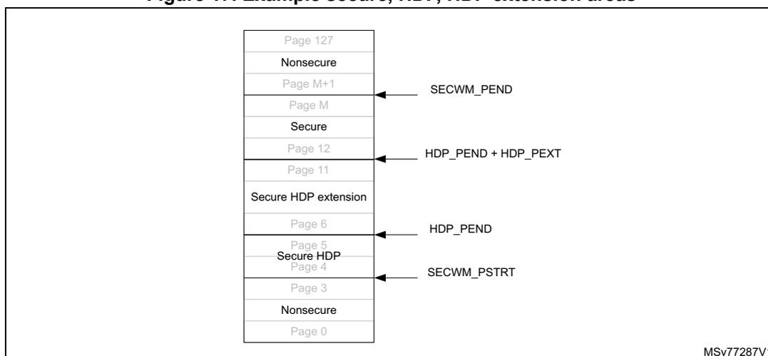
MSV77287V1
7.5.5 Block-based secure flash memory area protection
Any page can be programmed on the fly as secure or nonsecure using the block-based configuration registers FLASH_SECBBRx to configure the security attribute.
When the page security attribute, bit SECBBy in SECBBRx, is set, the security attribute is the same as the secure watermark-based area. The secure page is only accessible by a secure access.
If the SECBy bit in SECByR x is set or reset for a page already included in a secure watermark-based area, the page keeps the watermark-based protection security attributes.
To modify a block-based page security attribution, the following actions are recommended:
- • Check that no flash memory operation is ongoing on the related page.
- • Add an ISB instruction after modifying the page security attribute bit in SECByR x .
Caution: Switching a page or memory block from secure to nonsecure does not erase the content of the associated block. User secure software must perform the following needed operations before switching a block between secure and nonsecure attribute:
- • Erase page content,
- • Invalidate the instruction cache.
Note: For SECByR x bit i access control, refer to Table 68 .
7.5.6 Flash security attribute state
The flash memory is secure when at least one secure area is defined either by watermark-based option bytes or block-based security registers.
It is possible to override the flash security state using the INV bit in the FLASH_SECCR1 register.
The RCC FLASHEN and FLASHSMEN bits security attributes follow the flash memory security attribute. It is possible to override the flash memory security attribute in RCC using the INV bit in the FLASH_SECCR1 register. A secure firmware setting this INV bit allows a nonsecure firmware to disable the flash memory clock when the flash memory is in power down or when the MCU enters low-power modes.
Table 54. Flash security state
| Secure area | INV bit | Flash security state |
|---|---|---|
| None | 0 | Nonsecure |
| 1 | Secure | |
| Yes | 0 | Secure |
| 1 | Nonsecure |
7.5.7 Block-based privileged flash memory area protection
Any page can be programmed on the fly as privileged or unprivileged using the block-based configuration registers FLASH_PRIVByR x to configure the privilege attribute.
When the page privilege attribute, bit PRIVBy in PRIVByR x , is set, the page is only accessible by a privileged access. An unprivileged page is accessible by a privileged or unprivileged access.
To modify a block-based privilege attribution, the following actions are recommended:
- • Check that no flash operation is ongoing on the related page.
- • Add an ISB instruction after modifying the page security attribute bit in PRIVByR x .
Caution: Switching a page or memory block from privileged to unprivileged does not erase the content of the associated block.
Note: For PRIVByR x bit access control, refer to Table 69 and Table 70 .
7.5.8 Flash memory registers privileged and unprivileged modes
The flash memory registers can be read and written by privileged and unprivileged accesses depending on the SPRIV and NSPRIV bits in FLASH privilege configuration register (FLASH_PRIFCFGR) , with the following rules:
- • When the SPRIV (resp. NSPRIV) bit is reset, all secure (resp. nonsecure) flash memory registers can be read and written by both privileged or unprivileged access.
- • When the SPRIV (resp. NSPRIV) bit is set, all secure (resp. nonsecure) flash memory registers can be read and written by privileged access only. Unprivileged access to a privileged register is RAZ/WI.
Table 67 summarizes the flash memory a privileged register access control.
7.6 Flash memory protection
The flash memory interface implements the following protection mechanisms:
- • Readout protection (RDP)
- • Two write protection (WRP) nonvolatile areas
- • Additional secure protections when TrustZone is active (refer to
Section 7.5
)
- – One secure watermark-based nonvolatile area
- – One secure hide protection nonvolatile area
- – Secure block-based volatile areas with page granularity
- • Privileged block-based volatile areas with page granularity (refer to Section 7.5.7 )
7.6.1 Write protection (WRP)
The user area in flash memory can be protected against unwanted write operations. Two write-protected (WRP) areas can be defined, with page granularity.
Each area is defined by a start page offset and an end page offset related to the physical flash base address. These offsets are defined in the WRP address registers: FLASH WRP area A address register (FLASH_WRPAR) , and FLASH WRP area B address register (FLASH_WRPBR) .
The WRP “y” area (y = A,B) is defined as follows:
- • From the address: flash base address + [WRPy_PSTRT x 0x2000] (included)
- • To the address: flash base address + [(WRPy_PEND+1) x 0x2000] (excluded)
For example, to protect by WRP from the address 0x0806 2000 (included) to the address 0x0807 3FFF (included):
- • FLASH_WRPAR register must be programmed with:
- – WRPA_PSTRT = 0x62
- – WRPA_PEND = 0x73
WRPB_PSTRT and WRPB_PEND in FLASH_WRPBR can be used instead (area “B” in flash).
When WRP is active, protected flash memory pages cannot be erased or programmed. Consequently, a software mass erase cannot be performed if one area is write-protected.
If an erase/program operation to a write-protected part of the flash memory is attempted, the secure or nonsecure write protection error flag (WRPERR) is set in the FLASH_NSSR or
FLASH_SECSR register. This flag is also set for any write access to the system flash memory and to the OTP area.
Note: When the memory readout protection level 1 is selected (RDP level = 1), it is not possible to program or erase the flash memory (secure or nonsecure) if the CPU debug features are connected (JTAG or single wire) or boot code is being executed from RAM or system flash memory, even if WRP is not activated.
When the memory readout protection level 0.5 is selected (RDP level = 0.5), it is not possible to program or erase the flash secure memory if the CPU debug features are connected (JTAG or single wire), even if WRP is not activated.
Note: To validate the WRP options, the option bytes must be reloaded through the OBL_LAUNCH bit in the flash control register.
Table 55. WRP protection
| WRP registers values (y = A / B) | WRP area |
|---|---|
| WRPy_PSTRT = WRPy_PEND | Page WRPy is protected |
| WRPy_PSTRT > WRPy_PEND | No WRPy area |
| WRPy_PSTRT < WRPy_PEND | The pages from WRPy_PSTRT to WRPy_PEND are protected |
Write protection lock
Each WRP area can be independently locked by writing 0 to the UNLOCK bit in the FLASH WRP area A address register (FLASH_WPAR) , or FLASH WRP area B address register (FLASH_WPBR) . Once a WRP area is locked, it is not possible to modify its settings. In order to unlock a WRP area, a regression to RDP level 0 must be launched.
To make the WRP area immutable and act as a ROM, the following actions are needed:
- • If RDP level is 0, 0.5 or 1, provision an OEM1 key in order to prevent a regression to RDP level 0 for users not knowing the key.
- • If RDP level is 2, either provision an OEM1 key (refer to first bullet) or do not provision an OEM2 key (preventing regression from level 2 to level 1).
For more information on RDP regressions, refer to Device life cycle managed by readout protection (RDP) transitions .
7.6.2 Readout protection (RDP)
The readout protection protects the flash main memory, ICACHE, option bytes, backup registers, and the SRAMs.
Readout protection levels when Trustzone is disabled
There are three levels of readout protection from no protection (level 0) to maximum protection or no debug (level 2). The flash memory is protected according to the RDP option byte value shown in Table 56 .
Table 56. Flash memory readout protection status (TZEN=0)
| RDP byte value | Readout protection level |
|---|---|
| 0xAA | Level 0 |
| Any value except 0xAA or 0xCC | Level 1 |
| 0xCC | Level 2 |
- • Level 0: no protection
Read, program, and erase operations into the flash main memory area are possible. The option bytes, the SRAMs, and the backup registers are also accessible by all operations.
- • Level 1: readout protection
When the readout protection level 1 is set:
- – User mode: code executing in user mode ( boot flash ) can access the flash main memory, option bytes, SRAMs, and backup registers with all operations (read, erase, program).
- – Debug, boot RAM, and bootloader modes: in debug mode or when the microcontroller boots from RAM or system memory, the flash main memory, the backup registers, and the SRAM2 are totally inaccessible; any read or write access to the flash main memory generates a bus error and a hard fault interrupt. External memory on-the-fly decryption regions defined in OTFDEC are read as zero.
- • Level 2: no debug
When the readout protection level 2 is set:
- – The protection level 1 is guaranteed.
- – All debug features are disabled.
- - if OEM2 key has not been provided, JTAG and SWD are definitely disabled.
- - if OEM2 key has been provided, JTAG and SWD remain enabled under reset only to interface with DBGMCU_SR, DBGMCU_DBG_AUTH_HOST and DBG_MCU_AUTH_DEVICE registers to obtain device identification and provide OEM2 key to request RDP regression.
- – The boot from SRAM (boot RAM mode) and the boot from system memory (bootloader mode) are no longer available.
- – Only boot from the main flash memory is possible; all operations are allowed on the flash main memory. Read, erase, and program accesses to the flash memory and SRAMs from user code are allowed.
- – Option bytes cannot be programmed nor erased, any attempt to modify option bytes set the OPTWERR flag. Thus, the nonvolatile option areas can no longer be
modified, and level 2 cannot be removed: it is an irreversible operation unless an OEM2 key has been provisioned (refer to OEM2 RDP lock mechanism ).
Note: The debug feature is also disabled under reset.
STMicroelectronics is not able to perform analysis on defective parts on which the level 2 protection has been set. Regress parts to RDP level 1 before returning them for analysis (refer to OEM2 RDP lock mechanism ).
Table 57. Access status versus protection level and execution modes when TZEN = 0
| Area | RDP level | User execution (boot from flash) | Debug/boot from RAM/ bootloader (1) | ||||
|---|---|---|---|---|---|---|---|
| Read | Write | Erase | Read | Write | Erase | ||
| Flash main memory | 1 | Yes | Yes | Yes | No | No | No (4) |
| 2 | Yes | Yes | Yes | N/A | N/A | N/A | |
| System memory (2) | 1 | Yes | No | No | Yes | No | No |
| 2 | Yes | No | No | N/A | N/A | N/A | |
| Option bytes (3) | 1 | Yes | Yes (4) | N/A | Yes | Yes (4) | Yes |
| 2 | Yes | No | N/A | N/A | N/A | N/A | |
| OTP | 1 | Yes | Yes (5) | N/A | Yes | Yes (5) | N/A |
| 2 | Yes | Yes (5) | N/A | N/A | N/A | N/A | |
| Backup registers | 1 | Yes | Yes | N/A | No | No | N/A (6) |
| 2 | Yes | Yes | N/A | N/A | N/A | N/A | |
| SRAM2 | 1 | Yes | Yes | N/A | No | No | N/A (6) |
| 2 | Yes | Yes | N/A | N/A | N/A | N/A | |
| OTFDEC regions | 1 | Yes | Yes | Yes | No | Yes | Yes (7) |
| 2 | Yes | Yes | Yes | N/A | N/A | N/A | |
1. When the protection level 2 is active, the debug port, the boot from RAM and the boot from system memory are disabled.
2. The system memory is only read-accessible, whatever the protection level (0, 1 or 2) and execution mode.
3. Option bytes are only accessible through the flash registers interface and OPTSTRT bit.
4. The flash main memory is erased when the RDP option byte changes from level 1 to level 0.
5. OTP can only be written once.
6. All SRAMs and backup registers are erased when regressing RDP to level 0.
7. The OTFDEC keys are erased when regressing RDP to level 0.
Readout protection levels when Trustzone is enabled
There are four levels of readout protection from no protection (level 0) to maximum protection or no debug (level 2). The flash memory is protected according to the RDP option byte value shown in Table 56 .
Table 58. Flash memory readout protection status (TZEN = 1)
| RDP byte value | Readout protection level |
|---|---|
| 0xAA | Level 0 |
| 0x55 | Level 0.5 |
| Any value except 0xAA or 0x55 or 0xCC | Level 1 |
| 0xCC | Level 2 |
- • Level 0: no protection
Read, program and erase operations into the flash main memory area are possible. The option bytes, the SRAMs, and the backup registers are also accessible by all operations.
- – RSS mode: when booting from RSS, the debug access is disabled while executing RSS code.
- • Level 0.5: nonsecure debug only
All read and write operations (if no write protection is set) from/to the nonsecure flash memory are possible. The debug access to the secure area is prohibited. Debug access to nonsecure area remains possible.
- – User mode: code executing in user mode ( boot flash ) can access the flash main memory, option bytes, SRAMs, and backup registers with all operations (read, erase, program).
- – Nonsecure debug mode: nonsecure debug is possible when the CPU is in nonsecure state. The secure flash memory, the secure backup registers and SRAMs area are inaccessible; the nonsecure flash memory, the nonsecure backup registers, and the nonsecure SRAMs area remain accessible for debug purpose.
- – RSS mode: when booting from RSS, the debug access is disabled while executing RSS code.
- – Boot RAM mode: boot from SRAM is not possible.
- • Level 1: readout protection
When the readout protection level 1 is set:
- – User mode: code executing in user mode ( boot flash ) can access the flash main memory, option bytes, SRAMs, and backup registers with all operations (read, erase, program).
- – Nonsecure debug mode: nonsecure debug is possible when the CPU is in nonsecure state. However, an intrusion is detected in case of debug access: the flash main memory, the backup registers, and the SRAM2 are totally inaccessible; any read or write access to the flash main memory generates a bus error and a
hard fault interrupt. External memory on-the-fly decryption regions defined in OTFDEC are read as zero.
- – RSS mode: when booting from RSS, the debug access is disabled while executing RSS code.
- – Boot RAM mode: boot from SRAM is not possible.
- • Level 2: no debug
When the readout protection level 2 is set:- – The protection level 1 is guaranteed.
- – All debug features are disabled.
- - if OEM2 key has not been provided, JTAG and SWD are definitely disabled.
- - if OEM2 key has been provided, JTAG and SWD remain enabled under reset only to interface with DBGMCU_SR, DBGMCU_DBG_AUTH_HOST and DBG_MCU_AUTH_DEVICE registers to obtain device identification and provide OEM2 key to request RDP regression.
- – The boot from SRAM (boot RAM mode) and the boot from system memory (bootloader mode) are no longer available.
- – Boot from RSS is possible.
- – When booting from main flash or RSS, all operations are allowed on the flash main memory. Read, erase, and program accesses to flash memory and SRAMs from user code are allowed.
- – Option bytes cannot be programmed nor erased. Thus, the nonvolatile security areas SECWM, HDP, and WRP areas can no longer be modified, the level 2 cannot be removed: it is an irreversible operation unless an OEM2 key has been provisioned (refer to OEM2 RDP lock mechanism ).
Note: The debug feature is also disabled under reset.
STMicroelectronics is not able to perform analysis on defective parts on which the level 2 protection has been set. Regress parts to RDP level 1 before returning them for analysis (refer to OEM2 RDP lock mechanism ).
Table 59. Access status versus protection level and execution modes when TZEN = 1
| Area | RDP level | User execution (boot from flash) | Debug/bootloader (1) | ||||
|---|---|---|---|---|---|---|---|
| Read | Write | Erase | Read | Write | Erase | ||
| Flash main memory | 0.5 | Yes | Yes | Yes | Yes (2) | Yes (2) | Yes (2) |
| 1 | Yes | Yes | Yes | No | No | No (5) | |
| 2 | Yes | Yes | Yes | N/A | N/A | N/A | |
| System memory (3) | 0.5 | Yes | No | No | Yes | No | No |
| 1 | Yes | No | No | Yes | No | No | |
| 2 | Yes | No | No | N/A | N/A | N/A | |
| Option bytes (4) | 0.5 | Yes | Yes (5) | N/A | Yes | Yes (5) | Yes |
| 1 | Yes | Yes (5) | N/A | Yes | Yes (5) | Yes | |
| 2 | Yes | No | N/A | N/A | N/A | N/A | |
Table 59. Access status versus protection level and execution modes when TZEN = 1 (continued)
| Area | RDP level | User execution (boot from flash) | Debug/bootloader (1) | ||||
|---|---|---|---|---|---|---|---|
| Read | Write | Erase | Read | Write | Erase | ||
| OTP | 0.5 | Yes | Yes (6) | N/A | Yes | Yes (6) | N/A |
| 1 | Yes | Yes (6) | N/A | Yes | Yes (6) | N/A | |
| 2 | Yes | Yes (6) | N/A | N/A | N/A | N/A | |
| Backup registers | 0.5 | Yes | Yes | N/A | Yes (2) | Yes (2) | N/A (7) |
| 1 | Yes | Yes | N/A | No | No | N/A (7) | |
| 2 | Yes | Yes | N/A | N/A | N/A | N/A | |
| SRAM2 | 0.5 | Yes | Yes | N/A | Yes (2) | Yes (2) | N/A (7) |
| 1 | Yes | Yes | N/A | No | No | N/A (7) | |
| 2 | Yes | Yes | N/A | N/A | N/A | N/A | |
| OTFDEC regions | 0.5 | Yes | Yes | Yes | No | Yes | Yes (8) |
| 1 | Yes | Yes | Yes | No | Yes | Yes (8) | |
| 2 | Yes | Yes | Yes | N/A | N/A | N/A | |
- 1. When the protection level 2 is active, the debug port and the bootloader mode are disabled.
- 2. Depends on TrustZone security access rights.
- 3. The system memory is only read-accessible, whatever the protection level (0, 1 or 2) and execution mode.
- 4. Option bytes are only accessible through the flash registers interface and OPTSTRT bit.
- 5. The flash main memory is erased when the RDP option byte regresses from level 1 to level 0.
- 6. OTP can only be written once.
- 7. All SRAMs and TAMP backup registers are erased when regressing RDP to level 0.5 and level 0.
- 8. The OTFDEC keys are erased when regressing RDP to level 0.5 and level 0
Device life cycle managed by readout protection (RDP) transitions
It is easy to move from level 0 or level 0.5 to level 1 by changing the value of the RDP byte to any value (except 0xCC, 0xAA, and 0x55). By programming the 0xCC value in the RDP byte, it is possible to go to level 2 either directly from level 0 or from level 0.5 or from level 1. Once in level 2, it is no longer possible to modify the readout protection level unless an OEM2 key is provisioned (refer to OEM2 RDP lock mechanism ).
When the RDP is reprogrammed to the value 0xAA to move from level 1 to level 0, a mass erase of the flash main memory and SRAM1, SRAM2, ICACHE, PKA SRAM, TAMP backup registers, and OTFDEC keys is performed. The OTP area is not erased.
At RDP level 0.5, it is not possible to request RDP level 0. Instead, an RDP increase to level 1 followed by an RDP regression to level 0 is required.
When the RDP is programmed to the value 0x55 to move from level 1 to level 0.5, a partial mass erase of the flash main memory is performed. Only nonsecure watermark-based areas are erased (regardless if it is defined as secure by block-based). The SRAM1,
SRAM2, ICACHE, PKA SRAM, TAMP backup registers, and OTFDEC keys are mass erased. The OTP area is not erased. The RDP level 0.5 and partial nonsecure erase are only available when TrustZone is active.
Note: Full mass erase is performed only when level 1 is active and level 0 is requested. When the protection level is increased (0 to 0.5, 0 to 1, 0.5 to 1, 1 to 2, 0 to 2 or 0.5 to 2), there is no mass erase.
To validate the readout protection level change, the option bytes must be reloaded through the OBL_LAUNCH bit in FLASH control register (FLASH_NSCR1) .
Before launching an RDP regression, the software must invalidate the ICACHE and wait for the BUSYF bit to get cleared.
Figure 18. RDP level transition scheme when TrustZone is disabled (TZEN = 0)
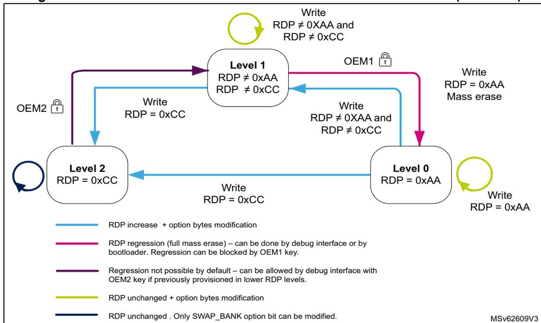
Legend:
- — RDP increase + option bytes modification
- — RDP regression (full mass erase) – can be done by debug interface or by bootloader. Regression can be blocked by OEM1 key.
- — Regression not possible by default – can be allowed by debug interface with OEM2 key if previously provisioned in lower RDP levels.
- — RDP unchanged + option bytes modification
- — RDP unchanged . Only SWAP_BANK option bit can be modified.
MSv62609V3
Figure 19. RDP level transition scheme when TrustZone is enabled (TZEN = 1)
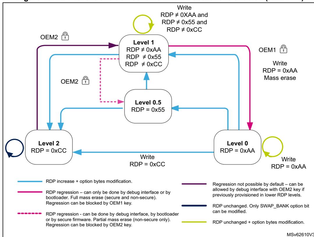
graph TD
    L0[Level 0
RDP = 0xAA] -- "Write RDP = 0xCC" --> L2[Level 2
RDP = 0xCC]
    L0 -- "Write RDP = 0x55" --> L05[Level 0.5
RDP = 0x55]
    L0 -- "Write RDP ≠ 0xAA, 0x55, 0xCC" --> L1[Level 1
RDP ≠ 0xAA, 0x55, 0xCC]
    L1 -- "Write RDP = 0xAA
Mass erase (OEM1)" --> L0
    L1 -- "Write RDP = 0x55
Partial mass erase (OEM2)" --> L05
    L05 -- "Write RDP ≠ 0xAA, 0x55, 0xCC" --> L1
    L1 -- "Write RDP = 0xCC" --> L2
    L2 -- "Write RDP = 0x55
(OEM2)" --> L05
    L0 -- "Write RDP = 0xAA" --> L0
    L1 -- "Write RDP ≠ 0xAA, 0x55, 0xCC" --> L1
    L2 -- "Write RDP = 0xCC" --> L2
Legend:
- — RDP increase + option bytes modification.
- — RDP regression – can only be done by debug interface or by bootloader. Full mass erase (secure and non-secure). Regression can be blocked by OEM1 key.
- - - - RDP regression - can be done by debug interface, by bootloader or by secure firmware. Partial mass erase (non-secure only). Regression can be blocked by OEM2 key.
- — Regression not possible by default – can be allowed by debug interface with OEM2 key if previously provisioned in lower RDP levels.
- — RDP unchanged. Only SWAP_BANK option bit can be modified.
- — RDP unchanged + option bytes modification.
MSv62610V3
OEM1/OEM2 lock activation
Two 128-bit keys (OEM1 key and OEM2 key) can be defined in order to lock the RDP regression. Each 128-bit key is coded on four registers:
- OEM1 key coded on:
- FLASH OEM1 key register 1 (FLASH_OEM1KEYR1)
- FLASH OEM1 key register 2 (FLASH_OEM1KEYR2)
- FLASH OEM1 key register 3 (FLASH_OEM1KEYR3)
- FLASH OEM1 key register 4 (FLASH_OEM1KEYR4)
- OEM2 key coded on:
- FLASH OEM2 key register 1 (FLASH_OEM2KEYR1)
- FLASH OEM2 key register 2 (FLASH_OEM2KEYR2)
- FLASH OEM2 key register 3 (FLASH_OEM2KEYR3)
- FLASH OEM2 key register 4 (FLASH_OEM2KEYR4)
OEM1 key and OEM2 key cannot be read through these registers but there are two 8-bit CRC OEM1KEYCRC and OEM2KEYCRC values which can be used as a public Key information.
Any read access to OEM1 key and OEM2 key returns zero.
OEM1 key can be modified in readout protection:
- • RDP level 0
- • RDP level 0.5 or 1 if OEM1LOCK = 0 in FLASH status register (FLASH_NSSR)
OEM2 key can be modified in readout protection:
- • RDP level 0 or 0.5
- • RDP level 1 if OEM2LOCK = 0 in FLASH status register (FLASH_NSSR)
When attempting to modify the OEM1 key registers or OEM2 key registers without following these rules, the user option modification is not done and the OPTWERR bit is set.
In order to activate the OEM1 key lock mechanism, the following steps are needed:
- 1. Check that the OEM1LOCK bit is not set or that the readout protection is at level 0.
- 2. Write a 128-bit OEM1 key in OEM1 key registers
- 3. Check key CRC in OEM1KEYCRC.
- 4. Launch option modification by setting the OPTSTRT bit in the FLASH control register (FLASH_NSCR1) .
- 5. Wait for the BSY bit to be cleared and check that OPTWERR is not set.
- 6. Set the OBL_LAUNCH option bit to start option bytes loading or perform a power-on reset.
- 7. Check that OEM1LOCK is set.
In order to activate the OEM2 key lock mechanism, the following steps are needed:
- 1. Check that the OEM2LOCK bit is not set or that the readout protection is at level 0 or 0.5.
- 2. Write a 128-bit OEM 2 key in OEM2 key registers.
- 3. Check key CRC in OEM2KEYCRC.
- 4. Launch option modification by setting the OPTSTRT bit in the FLASH control register (FLASH_NSCR1) .
- 5. Wait for the BSY bit to be cleared and check that OPTWERR is not set.
- 6. Set the OBL_LAUNCH option bit to start option bytes loading or perform a power-on reset.
- 7. Check that OEM2LOCK is set.
Note: The OEM1 key and OEM2 key must not contain more than four zero.
OEM1 RDP lock mechanism
The OEM1 key RDP lock mechanism is active when the OEM1LOCK bit is set. It conditions the RDP level 1 to RDP level 0 regression.
In order to regress from RDP level 1 to RDP level 0, the following sequence must be applied:
- • Shift OEM1 key bit[31:0] followed by subsequent OEM1 keys and last OEM1 key bit[127:96] through the JTAG or SWD under reset in the DBGMCU_DBG_AUTH_HOST register.
- – If this key is matching the OEM1KEY register value, the RDP regression can be launched by setting the OPTSTRT bit.
- – If the key is not matching the OEM1KEY register value, RDP regression and any access to the flash are blocked until a next power on reset.
Attempting to regress from RDP level 1 to RDP level 0 without following this sequence sets the OPTWERR flag and the option bytes remain unchanged.
When the lock mechanism is not activated (OEM1LOCK =0), the regression from RDP level 1 to RDP level 0 is always granted.
OEM2 RDP lock mechanism
The OEM2 key RDP lock mechanism is active when the OEM2LOCK bit is set. It allows the following actions:
- • Condition RDP level 1 to RDP level 0.5 regression.
- • Authorize RDP level 2 to RDP level 1 regression.
In order to regress from RDP level 1 to RDP level 0.5, the following unlock sequence must be applied:
- • Shift OEM2 key bits[31:0] followed by subsequent OEM2 keys and last OEM2 key bits[127:96] through the JTAG or SWD under reset in the DBGMCU_DBG_AUTH_HOST register.
- – If this key is matching the OEM2KEY register value, the RDP regression can be launched by setting the OPTSTRT bit.
- – If the key is not matching the OEM2KEY register value, RDP regression and any access to the flash are blocked until a next power on rest.
Attempting to regress from RDP level 1 to RDP level 0.5 without following this sequence, sets the OPTWERR flag and the option bytes remain unchanged.
To regress from RDP level 2 to RDP level 1, apply the following unlock sequence:
- • Shift OEM2 key bits[31:0] followed by subsequent OEM2 keys and last OEM2 key bits[127:96] through the JTAG or SWD under reset in the DBGMCU_DBG_AUTH_HOST register.
- – If this key is matching the OEM2KEY register value, the RDP regression is launched by hardware (it is not possible to execute instructions when the key is matching). Subsequently apply a power-on reset (cycle V DD power supply OFF and ON).
- – If the key is not matching the OEM2KEY register value, RDP regression and any access to the flash are blocked until a next power on rest.
Attempting to regress from RDP level 2 to RDP level 1 without following this sequence, leaves option bytes unchanged.
When the lock mechanism is not activated (OEM2LOCK =0), the following happens:
- • The regression from RDP level 1 to RDP level 0.5 is always granted.
- • The regression from RDP level 2 to RDP level 1 is never granted. When attempting to modify the options bytes, the OPTWERR flag is set and the option bytes remain unchanged.
OEM key CRC source
Below is the CRC source code that can be used to compare with the result of the computation provided by the flash interface in OEM1KEYCRC and OEM2KEYCRC fields, after loading the keys in OEM1 key and OEM2 key registers.
uint8_t getCRC(uint32_t * keyin)
{
    const uint8_t CRC7_POLY = 0x7;
    const uint32_t key_strobe[4] = {0xAA55AA55, 0x3, 0x18, 0xC0};
uint8_t i, j, k, crc = 0x0;
uint32_t keyval;
for (j = 0; j < 4; j++)
{keyval = * (keyin+j);
if (j == 0) { keyval ^= key_strobe[0]; }
else { keyval ^= (key_strobe[j] << 24) | (crc << 16) | (key_strobe[j] << 8)
| crc; }
for (i = 0, crc = 0; i < 32; i++)
{
k = (((crc >> 7) ^ (keyc=val >> (31-i))&0xF)) & 1;
crc <<= 1;
if (k) { crc ^= CRC7_POLY; }
}
crc^=0x55;
}
return crc;
}
7.7 Summary of flash memory and registers access control
The following tables summarize the flash memory and registers accesses status versus RDP level, WRP, and HDP protections.
Table 60. Flash memory access versus RDP level when TrustZone is active (TZEN = 1)
| Access type | RDP level 0, RDP level 0.5, RDP level 1 no intrusion (1) or RDP level 2 | RDP level 1 with intrusion (2) | |||
|---|---|---|---|---|---|
| Nonsecure page | Secure page | Nonsecure or secure page | |||
| HDP and HDP extension areas, ACCDIS disabled | Others (3) | ||||
| Secure | Fetch | Bus error | RAZ | OK | Bus error |
| Read | RAZ, flash illegal access event | ||||
| Write | WI, secure WRPERR flag set, flash illegal access event | WI, secure WRPERR flag set | No WRP: OK WRP pages: WI and secure WRPERR flag set | WI, secure WRPERR flag set | |
| Page erase | |||||
| Nonsecure | Fetch | OK | Bus error | Bus error | |
| Read | RAZ, flash illegal access event | ||||
| Write | No WRP: OK | WI, nonsecure WRPERR flag set, flash illegal access event | WI, nonsecure WRPERR flag set | ||
| Page erase | WRP pages: WI and nonsecure WRPERR flag set | ||||
1. RDP level 1 no intrusion: when booting from user flash memory and no debug access.
2. RDP level 1 with intrusion: when debug access detected.
3. Refers to flash memory secure configurations different from the one described for HDP protections. Example: flash memory secure and HDP area enabled but ACCDIS = enabled.
Table 61. Flash memory secure access versus HDP and HDP extension (TZEN = 1)
| Access type | HDP area | HDP extension area | Other |
|---|---|---|---|
| Fetch | OK when HDP access is enabled. Else RAZ | OK when HDP area access is disabled and HDP extension access is enabled. Else RAZ | OK when HDP and HDP extension access are disabled. Else RAZ |
| Read | OK when HDP access is enabled. Else RAZ | OK when HDP extension access is enabled. Else RAZ | OK |
| Write | OK if HDP access is enabled. Else WI, secure WRPERR flag set | OK when HDP extension access is enabled. Else WI, secure WRPERR flag set | OK |
| Page erase |
Table 62. Flash memory access versus RDP level when TrustZone is disabled (TZEN = 0)
| Access type | RDP level 0, RDP level1 no intrusion (1) or RDP level 2 | RDP level 1 with intrusion (2) |
|---|---|---|
| Fetch | OK | Bus error |
| Read | ||
| Write | No WRP: OK | |
| Erase | WRP pages: WI and nonsecure WRPERR flag set | WI and nonsecure WRPERR flag set |
1. RDP Level 1 no intrusion: when booting from user flash memory and no debug access.
2. RDP Level 1 with intrusion: when booting from RAM or system memory or debug access detected.
Table 63. Flash memory mass erase versus RDP level when TrustZone is active (TZEN = 1)
| Access type | RDP level 0, RDP level 0.5, RDP level 1 no intrusion (1) or RDP level 2 | RDP level 1 with intrusion (2) | ||||
|---|---|---|---|---|---|---|
| Nonsecure flash | Secure flash | Mix nonsecure and secure flash memory | Nonsecure or secure flash memory | |||
| HDP area (HDPEN disable and ACCDIS disable) | Others (3) | |||||
| Secure | Mass erase | WI, secure WRPERR flag set, flash memory illegal access event | WI, secure WRPERR flag set | No WRP: OK WRP pages: WI and secure WRPERR flag set | WI, secure WRPERR flag set, flash memory illegal access event | WI, secure WRPERR flag set |
| Nonsecure | Mass erase | No WRP: OK WRP pages: WI and nonsecure WRPERR flag set | WI, nonsecure WRPERR flag set, flash memory illegal access event | WI, nonsecure WRPERR flag set | ||
- 1. RDP Level 1 no intrusion: when booting from user flash memory and no debug access.
- 2. RDP Level 1 with intrusion: when debug access detected.
- 3. "Others" refers to flash memory secure configurations different from the one described for HDP protections. Example: flash memory secure and HDP area enabled but ACCDIS = enabled.
| Access type | System memory (bootloader) | OTP (2) | RSS | |
|---|---|---|---|---|
| Secure (TZEN = 1) | Fetch | Bus error | RAZ | |
| Read | RAZ, flash memory register illegal access event | OK | ||
| Write | WI, secure WRPERR flag set, flash memory illegal access event | |||
| Nonsecure (TZEN = 0 or TZEN = 1) | Fetch | OK | Bus error | Bus error |
| Read | OK | RAZ (3) | ||
| Write | WI and nonsecure WRPERR flag set | OK if not virgin: WI, nonsecure PROGERR flag set | WI, nonsecure WRPERR flag set | |
- 1. Valid for all RDP levels.
- 2. Write to a nonvirgin OTP generates a PGSERR.
- 3. Flash memory illegal access event is generated when TZEN = 1.
| Access type | Unprivileged page | Privileged page | |
|---|---|---|---|
| Fetch, Read/Write, Page erase | Privileged | OK | |
| Fetch, Read | Unprivileged | OK | RAZ |
| Write, Page erase | Unprivileged | WI, secure or nonsecure WRPERR flag set | |
1. When TZEN = 1, access must be granted by security firewall before privilege is considered.
Table 66. Flash mass erase versus privilege mode (1)| Access type | Unprivileged flash memory | Privileged flash memory | Mix unprivileged and privileged flash memory | |
|---|---|---|---|---|
| Mass erase | Privileged | OK | ||
| Mass erase | Unprivileged | OK | WI, secure or nonsecure WRPERR flag set | |
1. When TZEN = 1, access must be granted by security firewall before privilege is considered.
Table 67. Flash registers access (1)| Access type | Nonsecure register | Secure register | ||||
|---|---|---|---|---|---|---|
| NSPRIV = 1 | NSPRIV = 0 | SPRIV = 1 | SPRIV = 0 | |||
| Fetch | Secure/ nonsecure | Privileged/ unprivileged | Bus error | |||
| Read/ Write | Secure (2) | Privileged | OK | |||
| Unprivileged | RAZ/WI | OK | RAZ/WI | OK | ||
| Nonsecure (3) | Privileged | OK | RAZ/WI and a flash memory register illegal access event (4) | |||
| Unprivileged | RAZ/WI | OK | ||||
1. Except SECBBRx, PRIVBBRx and PRIVCFGGR registers.
2. Secure access is valid only when TrustZone is active (TZEN = 1).
3. Nonsecure accesses are valid when TrustZone is active or disabled.
4. Flash register illegal access event is generated only when TZEN = 1.
Table 68. SECBBRx registers access when TrustZone is active (TZEN = 1)| Access type | Bit y in PRIVBBRx | Bit y in SECBBRx | ||
|---|---|---|---|---|
| Fetch | Secure/nonsecure | Privileged/unprivileged | - | Bus error |
| Read | Secure/nonsecure | Privileged/unprivileged | - | OK |
Table 68. SECBBRx registers access when TrustZone is active (TZEN = 1) (continued)
| Access type | Bit y in PRIVBBRx | Bit y in SECBBRx | ||
|---|---|---|---|---|
| Write | Secure | Privileged | x | OK |
| Unprivileged | 0 | OK for bit y | ||
| Unprivileged | 1 | WI for bit y | ||
| Nonsecure | Privileged/unprivileged | x | WI and a flash memory register illegal access event | |
Table 69. PRIVBBRx registers access when TrustZone is active (TZEN = 1)
| Access type | Page secure state (watermark or blocked based) | Bit y in PRIVBBRx | ||
|---|---|---|---|---|
| Fetch | Privileged/unprivileged | Secure/nonsecure | - | Bus error |
| Read | Privileged/unprivileged | Secure/nonsecure | - | OK for all bits |
| Write | Privileged | Secured | - | OK for all bits |
| Nonsecure | Nonsecure | OK for bit y | ||
| Nonsecure | Secure | WI for bit y | ||
| Unprivileged | Secured/nonsecure | - | WI for all bits | |
Table 70. PRIVBBRx registers access when TrustZone is disabled (TZEN = 0)
| Access type | PRIVBBRx | |
|---|---|---|
| Fetch | Privileged/unprivileged | Bus error |
| Read | Privileged/unprivileged | OK |
| Write | Privileged | OK |
| Unprivileged | WI | |
7.8 FLASH interrupts
Table 71. Flash interrupt requests
| Interrupt vector | Interrupt event | Event flag | Event flag/interrupt clearing method | Interrupt enable control bit | Exit Sleep mode | Exit Stop and Standby modes |
|---|---|---|---|---|---|---|
| FLASH_S | Secure end of operation | Secure EOP (1) | Write secure EOP = 1 | Secure EOPIE | Yes | No |
| Secure operation error | Secure OPERR (2) | Write secure OPERR = 1 | Secure ERRIE | Yes | No |
Table 71. Flash interrupt requests (continued)
| Interrupt vector | Interrupt event | Event flag | Event flag/interrupt clearing method | Interrupt enable control bit | Exit Sleep mode | Exit Stop and Standby modes |
|---|---|---|---|---|---|---|
| FLASH | Nonsecure end of operation | Nonsecure EOP (1) | Write nonsecure EOP = 1 | Nonsecure EOPIE | Yes | No |
| Nonsecure operation error | Nonsecure OPERR (2) | Write nonsecure OPERR = 1 | Nonsecure ERRIE | Yes | No | |
| ECC correction | ECCC | Write ECCC=1 | ECCCIE | Yes | No |
1. Secure EOP (resp. nonsecure EOP) is set only if secure EOPIE (resp. nonsecure EOPIE) is set.
2. Secure OPERR (resp. nonsecure OPERR) is set only if secure ERRIE (resp. nonsecure ERRIE) is set.
7.9 FLASH registers
7.9.1 FLASH access control register (FLASH_ACR)
Address offset: 0x000
Reset value: 0x0000 0001
Access: no wait state when no flash memory read is ongoing; word, half-word and byte access
| 31 | 30 | 29 | 28 | 27 | 26 | 25 | 24 | 23 | 22 | 21 | 20 | 19 | 18 | 17 | 16 |
|---|---|---|---|---|---|---|---|---|---|---|---|---|---|---|---|
| Res. | Res. | Res. | Res. | Res. | Res. | Res. | Res. | Res. | Res. | Res. | Res. | Res. | Res. | Res. | Res. |
| 15 | 14 | 13 | 12 | 11 | 10 | 9 | 8 | 7 | 6 | 5 | 4 | 3 | 2 | 1 | 0 |
| Res. | SLEEP_PD | Res. | PDREQ | LPM | Res. | Res. | PRFTEN | Res. | Res. | Res. | Res. | LATENCY[3:0] | |||
| rw | rs | rw | rw | rw | rw | rw | rw | ||||||||
Bits 31:15 Reserved, must be kept at reset value.
Bit 14 SLEEP_PD : Flash memory power-down mode during Sleep mode
This bit determines whether the flash memory is in power-down mode or Idle mode when the device is in Sleep mode.
Access to the bit can be secured by PWR LPMSEC. When secure, a nonsecure read/write access is RAZ/WI. It does not generate an illegal access interrupt. This bit can be protected against unprivileged access when secure with FLASH SPRIV or when nonsecure with FLASH NSPRIV.
0: Flash in idle mode during Sleep mode
1: Flash in power-down mode during Sleep mode
Caution: The flash must not be put in power-down while a program or an erase operation is ongoing.
Caution: DMA can-not access the flash when in power-down mode. The DMA access to flash will be staled until the flash is taken out of power-down mode by a CPU wake-up. When the DMA needs to access flash while the CPU is in Sleep mode, SLEEP_PD must be 0.
Bit 13 Reserved, must be kept at reset value.
Bit 12 PDREQ : Flash power-down mode request
This bit requests flash to enter power-down mode. When flash enters power-down mode, this bit is cleared by hardware and the PDKEYR is locked.
This bit is write-protected with FLASH_PDKEYR.
Access to the bit can be secured by PWR LPMSEC. When secure, a nonsecure read/write access is RAZ/WI. It does not generate an illegal access interrupt. This bit can be protected against unprivileged access when secure with FLASH SPRIV or when nonsecure with FLASH NSPRIV.
0: No request for flash to enter power-down mode
1: Flash requested to enter power-down mode
Bit 11 LPM : Low-power read mode
This bit puts the flash memory in low-power read mode.
Access to the bit can be secured by PWR LPMSEC. When secure, a nonsecure read/write access is RAZ/WI. It does not generate an illegal access interrupt. This bit can be protected against unprivileged access when secure with FLASH SPRIV or when nonsecure with FLASH NSPRIV.
This bit cannot be written when a flash program or erase operation is busy (BSY = 1), or when the write buffer is not empty (WDW = 1). Changing this bit while a flash program or erase operation is busy (BSY = 1) is rejected.
- 0: Flash not in low-power read mode
- 1: Flash in low-power read mode
Bits 10:9 Reserved, must be kept at reset value.
Bit 8 PRFTEN : Prefetch enable
This bit enables the prefetch buffer in the embedded flash memory.
This bit can be protected against unprivileged access by FLASH NSPRIV.
- 0: Prefetch disabled
- 1: Prefetch enabled
Bits 7:4 Reserved, must be kept at reset value.
Bits 3:0 LATENCY[3:0] : Latency
These bits represent the ratio between the AHB hclk1 clock period and the flash memory access time.
Access to the bit can be secured by RCC SYSCLKSEC. When secure, a nonsecure read/write access is RAZ/WI. It does not generate an illegal access interrupt. This bit can be protected against unprivileged access when secure with FLASH SPRIV or when nonsecure with FLASH NSPRIV.
- 0000: Zero wait state
- 0001: One wait state
- 0010: Two wait states
- ...
- 1111: Fifteen wait states
Note: Before entering Stop 1, 2, and 3 mode software must set FLASH wait state latency to at least 1.
7.9.2 FLASH key register (FLASH_NSKEYR)
Address offset: 0x008
Reset value: 0x0000 0000
Access: one wait state; word access
This register is nonsecure. It can be read and written by both secure and nonsecure access. This register can be protected against unprivileged access when NSPRIV = 1 in the FLASH_PRIVCFGR register.

| 31 | 30 | 29 | 28 | 27 | 26 | 25 | 24 | 23 | 22 | 21 | 20 | 19 | 18 | 17 | 16 |
| NSKEY[31:16] | |||||||||||||||
| w | w | w | w | w | w | w | w | w | w | w | w | w | w | w | w |
| 15 | 14 | 13 | 12 | 11 | 10 | 9 | 8 | 7 | 6 | 5 | 4 | 3 | 2 | 1 | 0 |
| NSKEY[15:0] | |||||||||||||||
| w | w | w | w | w | w | w | w | w | w | w | w | w | w | w | w |
Bits 31:0 NSKEY[31:0] : Flash memory nonsecure key
The following values must be written consecutively to unlock the FLASH_NSCR1 register, allowing the flash memory nonsecure programming/erasing operations:
KEY1: 0x4567 0123
KEY2: 0xCDEF 89AB
7.9.3 FLASH secure key register (FLASH_SECKEYR)
Address offset: 0x00C
Reset value: 0x0000 0000
Access: one wait state; word access
This register is secure. It can be read and written only by secure access. A nonsecure read/write access is RAZ/WI. This register can be protected against unprivileged access when SPRIV = 1 in the FLASH_PRIVCFGR register.

| 31 | 30 | 29 | 28 | 27 | 26 | 25 | 24 | 23 | 22 | 21 | 20 | 19 | 18 | 17 | 16 |
| SECKEY[31:16] | |||||||||||||||
| w | w | w | w | w | w | w | w | w | w | w | w | w | w | w | w |
| 15 | 14 | 13 | 12 | 11 | 10 | 9 | 8 | 7 | 6 | 5 | 4 | 3 | 2 | 1 | 0 |
| SECKEY[15:0] | |||||||||||||||
| w | w | w | w | w | w | w | w | w | w | w | w | w | w | w | w |
Bits 31:0 SECKEY[31:0] : Flash memory secure key
The following values must be written consecutively to unlock the FLASH_SECCR1 register, allowing the flash memory secure programming/erasing operations:
KEY1: 0x4567 0123
KEY2: 0xCDEF 89AB
7.9.4 FLASH option key register (FLASH_OPTKEYR)
Address offset: 0x010
Reset value: 0x0000 0000
Access: one wait state; word access
This register is nonsecure. It can be read and written by both secure and nonsecure access. This register can be protected against unprivileged access when NSPRIV = 1 in the FLASH_PRIVCFGR register.

| 31 | 30 | 29 | 28 | 27 | 26 | 25 | 24 | 23 | 22 | 21 | 20 | 19 | 18 | 17 | 16 |
| OPTKEY[31:16] | |||||||||||||||
| w | w | w | w | w | w | w | w | w | w | w | w | w | w | w | w |
| 15 | 14 | 13 | 12 | 11 | 10 | 9 | 8 | 7 | 6 | 5 | 4 | 3 | 2 | 1 | 0 |
| OPTKEY[15:0] | |||||||||||||||
| w | w | w | w | w | w | w | w | w | w | w | w | w | w | w | w |
Bits 31:0 OPTKEY[31:0] : Option byte key
The LOCK bit in the FLASH_NSCR1 must be cleared before doing the unlock sequence for OPTLOCK bit. The following values must be written consecutively to unlock the FLASH_NSCR1.OPTSTRT and OBL_LAUNCH register bits concerning user option operations:
KEY1: 0x0819 2A3B
KEY2: 0x4C5D 6E7F
7.9.5 FLASH power-down key register (FLASH_PDKEYR)
Address offset: 0x018
Reset value: 0x0000 0000
Access: no wait state; word access
Access to this register can be protected by PWR_LPMSEC. When secure it can be read and written only by secure access. A nonsecure read/write access is RAZ/WI. This register can be protected against unprivileged access when secure by SPRIV = 1 and when nonsecure by NSPRIV in the FLASH_PRIVCFGR register.
| 31 | 30 | 29 | 28 | 27 | 26 | 25 | 24 | 23 | 22 | 21 | 20 | 19 | 18 | 17 | 16 |
|---|---|---|---|---|---|---|---|---|---|---|---|---|---|---|---|
| PDKEY1[31:16] | |||||||||||||||
| w | w | w | w | w | w | w | w | w | w | w | w | w | w | w | w |
| 15 | 14 | 13 | 12 | 11 | 10 | 9 | 8 | 7 | 6 | 5 | 4 | 3 | 2 | 1 | 0 |
| PDKEY1[15:0] | |||||||||||||||
| w | w | w | w | w | w | w | w | w | w | w | w | w | w | w | w |
Bits 31:0 PDKEY1[31:0] : Flash power-down key
The following values must be written consecutively to unlock the PDREQ bit in FLASH_ACR:
PDKEY_1: 0x0415 2637
PDKEY_2: 0xFAFB FCFD
7.9.6 FLASH status register (FLASH_NSSR)
Address offset: 0x020
Reset value: 0x000X 0000
Access: no wait state; word, half-word, and byte access
This register is nonsecure. It can be read and written by both secure and nonsecure access. This register can be protected against unprivileged access when NSPRIV = 1 in the FLASH_PRIVCFGR register.
| 31 | 30 | 29 | 28 | 27 | 26 | 25 | 24 | 23 | 22 | 21 | 20 | 19 | 18 | 17 | 16 |
|---|---|---|---|---|---|---|---|---|---|---|---|---|---|---|---|
| Res. | Res. | Res. | Res. | Res. | OPBRK | Res. | Res. | Res. | Res. | Res. | PD | OEM2LOCK | OEM1LOCK | WDW | BSY |
| rc_w1 | r | r | r | r | r | ||||||||||
| 15 | 14 | 13 | 12 | 11 | 10 | 9 | 8 | 7 | 6 | 5 | 4 | 3 | 2 | 1 | 0 |
| Res. | Res. | OPTWERR | Res. | Res. | Res. | Res. | Res. | PGSER | SIZER | PGAER | WRPER | PROGERR | Res. | OPER | EOP |
| rc_w1 | rc_w1 | rc_w1 | rc_w1 | rc_w1 | rc_w1 | rc_w1 | rc_w1 |
Bits 31:27 Reserved, must be kept at reset value.
Bit 26 OPBRK : Nonsecure flash operation aborted
This bit indicates that a flash nonsecure operation is aborted. It is cleared by writing 1.
Flash operation abort information in FLASH_OPSR shall be read when OPBRK is set.
Clearing OPBRK will also clear FLASH_OPSR.
Bits 25:21 Reserved, must be kept at reset value.
Bit 20 PD : Flash in power-down mode
This bit indicates that the flash memory is in power-down state. It is reset when flash is in normal mode or being awaken.
Bit 19 OEM2LOCK : OEM2 key RDP lock
This bit indicates that the OEM2 key read during the OBL is not virgin. When set, the OEM2 key RDP lock mechanism is active.
Bit 18 OEM1LOCK : OEM1 key RDP lock
This bit indicates that the OEM1 key read during the OBL is not virgin. When set, the OEM1 key RDP lock mechanism is active.
Bit 17 WDW : Nonsecure wait data to write
This bit indicates that the flash memory write buffer has been written by a secure or nonsecure operation. It is set when the first data is stored in the buffer and cleared when the write is performed in the flash memory.
Bit 16 BSY : Nonsecure busy
This indicates that a flash memory secure or nonsecure operation is in progress. This bit is set at the beginning of a flash operation and reset when the operation finishes or when an error occurs.
Bits 15:14 Reserved, must be kept at reset value.
Bit 13 OPTWERR : Option write error
This bit is set by hardware when the options bytes are written with an invalid configuration or when modifying options in RDP level 2. It is cleared by writing 1.
Refer to
Section 7.3.11
for full conditions of error flag setting.
Bits 12:8 Reserved, must be kept at reset value.
Bit 7 PGSERR : Nonsecure programming sequence error
This bit is set by hardware when programming sequence is not correct. It is cleared by writing 1.
Refer to
Section 7.3.11
for full conditions of error flag setting.
Bit 6 SIZERR : Nonsecure size error
This bit is set by hardware when the size of the access is a byte or half-word during a nonsecure program sequence. Only double-word programming is allowed by means of successive word accesses. This bit is cleared by writing 1.
Bit 5 PGAERR : Nonsecure programming alignment error
This bit is set by hardware when the first word to be programmed is not aligned with a double-word address, or the second word does not belong to the same double-word address. This bit is cleared by writing 1.
Bit 4 WRPERR : Nonsecure write protection error
This bit is set by hardware when a nonsecure address to be erased/programmed belongs to a write-protected part (by WRP or is secure) of the flash memory. This bit is cleared by writing 1.
Refer to
Section 7.3.11
for full conditions of error flag setting.
Bit 3 PROGERR : Nonsecure programming error
This bit is set by hardware when a nonsecure double-word address to be programmed contains a value different from all 1 before programming, except if the data to write is all 0. This bit is cleared by writing 1.
Bit 2 Reserved, must be kept at reset value.
Bit 1 OPERR : Nonsecure operation error
This bit is set by hardware when a flash memory nonsecure operation (program/erase) completes unsuccessfully. This bit is set only if nonsecure error interrupts are enabled (NSERRIE = 1). This bit is cleared by writing 1.
Bit 0 EOP : Nonsecure end of operation
This bit is set by hardware when one or more flash memory nonsecure operation (program/erase) has been completed successfully. This bit is set only if the nonsecure end of operation interrupts are enabled (EOPIE = 1 in FLASH_NSCR1). This bit is cleared by writing 1.
7.9.7 FLASH secure status register (FLASH_SECSR)
Address offset: 0x024
Reset value: 0x0000 0000
Access: no wait state; word, half-word, and byte access
This register is secure. It can be read and written only by secure access. A nonsecure read/write access is RAZ/WI. This register can be protected against unprivileged access when SPRIV = 1 in the FLASH_PRIVCFG register.
| 31 | 30 | 29 | 28 | 27 | 26 | 25 | 24 | 23 | 22 | 21 | 20 | 19 | 18 | 17 | 16 |
|---|---|---|---|---|---|---|---|---|---|---|---|---|---|---|---|
| Res. | Res. | Res. | Res. | Res. | OPBRK | Res. | Res. | Res. | Res. | Res. | Res. | Res. | Res. | WDW | BSY |
| rc_w1 | r | r | |||||||||||||
| 15 | 14 | 13 | 12 | 11 | 10 | 9 | 8 | 7 | 6 | 5 | 4 | 3 | 2 | 1 | 0 |
| Res. | Res. | Res. | Res. | Res. | Res. | Res. | Res. | PGSER | SIZER | PGAER | WRPE | PROG | Res. | OPER | EOP |
| R | R | R | RR | ERR | R | ||||||||||
| rc_w1 | rc_w1 | rc_w1 | rc_w1 | rc_w1 | rc_w1 | rc_w1 |
Bits 31:27 Reserved, must be kept at reset value.
Bit 26 OPBRK : Secure flash operation aborted
This bit indicates that a flash secure operation is aborted. It is cleared by writing 1. Flash operation abort information in FLASH_OPSR shall be read when OPBRK is set. Clearing OPBRK will also clear FLASH_OPSR.
Bits 25:18 Reserved, must be kept at reset value.
Bit 17 WDW : Secure wait data to write
This bit indicates that the flash memory write buffer has been written by a secure or nonsecure operation. It is set when the first data is stored in the buffer and cleared when the write is performed in the flash memory.
Bit 16 BSY : Secure busy
This bit indicates that a flash memory secure or nonsecure operation is in progress. This is set on the beginning of a flash operation and reset when the operation finishes or when an error occurs.
Bits 15:8 Reserved, must be kept at reset value.
Bit 7 PGSERR: Secure programming sequence errorThis bit is set by hardware when programming sequence is not correct. It is cleared by writing 1.
Refer to Section 7.3.11: Flash memory errors flags for full conditions of error flag setting.
Bit 6 SIZERR: Secure size errorThis bit is set by hardware when the size of the access is a byte or half-word during a secure program sequence. Only double-word programming is allowed by means of successive word accesses. This bit is cleared by writing 1.
Bit 5 PGAERR: Secure programming alignment errorThis bit is set by hardware when the first word to be programmed is not aligned with a double-word address, or the second, third or forth word does not belong to the same double-word address. This bit is cleared by writing 1.
Bit 4 WRPERR: Secure write protection errorThis bit is set by hardware when an secure address to be erased/programmed belongs to a write-protected part (by WRP, HDP or HDP extension) of the flash memory. This bit is cleared by writing 1.
Refer to Section 7.3.11 for full conditions of error flag setting.
Bit 3 PROGERR: Secure programming errorThis bit is set by hardware when a secure double-word address to be programmed contains a value different from all 1 before programming, except if the data to write is all 0. This bit is cleared by writing 1.
Bit 2 Reserved, must be kept at reset value. Bit 1 OPERR: Secure operation errorThis bit is set by hardware when a flash memory secure operation (program/erase) completes unsuccessfully. This bit is set only if secure error interrupts are enabled (SECERRIE = 1). This bit is cleared by writing 1.
Bit 0 EOP: Secure end of operationThis bit is set by hardware when one or more flash memory secure operation (program/erase) has been completed successfully. This bit is set only if the secure end of operation interrupts are enabled (EOPIE = 1 in FLASH_SECCR1). This bit is cleared by writing 1.
7.9.8 FLASH control register (FLASH_NSCR1)
Address offset: 0x028
Reset value: 0xC000 0000
Access: no wait state when no flash memory operation is ongoing; word, half-word, and byte access
This register is write protected with LOCK and must be unlocked by the NSKEY unlock sequence.
This register can only be written when the BSY or OBL_LAUNCH are reset. Otherwise, the write access is ignored and generates a bus error and hard fault interrupt.
This register is nonsecure. It can be read and written by both secure and nonsecure access. This register can be protected against unprivileged access when NSPRIV = 1 in the FLASH_PRIVCFG register.
| 31 | 30 | 29 | 28 | 27 | 26 | 25 | 24 | 23 | 22 | 21 | 20 | 19 | 18 | 17 | 16 |
|---|---|---|---|---|---|---|---|---|---|---|---|---|---|---|---|
| LOCK | OPTLOCK | Res. | Res. | OBL_LAUNCH | Res. | ERRIE | EOPIE | Res. | Res. | Res. | Res. | Res. | Res. | OPTSTART | STRT |
| rs | rs | rc_w1 | rw | rw | rs | rs | |||||||||
| 15 | 14 | 13 | 12 | 11 | 10 | 9 | 8 | 7 | 6 | 5 | 4 | 3 | 2 | 1 | 0 |
| Res. | BWR | Res. | Res. | Res. | Res. | PNB[6:0] | MER | PER | PG | ||||||
| rw | rw | rw | rw | rw | rw | rw | rw | rw | rw | rw | |||||
Bit 31 LOCK : Nonsecure lock
This bit is set only.
When set, the FLASH_NSCR1 register write access is locked. This bit is cleared by hardware after detecting the unlock sequence in FLASH_NSKEYR.
In case of an unsuccessful unlock operation, this bit remains set until the next system reset.
Bit 30 OPTLOCK : Option lock
This bit is set only. When set, the FLASH_NSCR1.OPTSTART and OBL_LAUNCH bits concerning user options write access is locked. This bit is cleared by hardware after detecting the unlock sequence in FLASH_OPTKEYR. The FLASH_NSCR1.LOCK bit must be cleared before doing the FLASH_OPTKEYR unlock sequence.
In case of an unsuccessful unlock operation, this bit remains set until the next reset.
Bits 29:28 Reserved, must be kept at reset value.
Bit 27 OBL_LAUNCH : Force the option byte loading
When set to 1, this bit forces the option byte reloading. This bit is cleared only when the option byte loading is complete. This bit is write-protected with OPTLOCK.
0: Option byte loading complete
1: Option byte loading requested
Note: The LSE oscillator must be disabled, LSEON = 0 and LSERDY = 0, before starting OBL_LAUNCH.
Bit 26 Reserved, must be kept at reset value.
Bit 25 ERRIE : Nonsecure error interrupt enable
This bit enables the interrupt generation when the OPERR bit in the FLASH_NSSR is set to 1.
0: Nonsecure OPERR error interrupt disabled
1: Nonsecure OPERR error interrupt enabled
Bit 24 EOPIE : Nonsecure end of operation interrupt enable
This bit enables the interrupt generation when the EOP bit in the FLASH_NSSR is set to 1.
0: Nonsecure EOP Interrupt disabled
1: Nonsecure EOP Interrupt enabled
Bits 23:18 Reserved, must be kept at reset value.
Bit 17 OPTSTRT : Options modification start
This bit triggers an option bytes erase and program operation when set. This bit is write-protected with OPTLOCK.. This bit is set only by software, and is cleared when the BSY bit is cleared in FLASH_NSSR.
Bit 16 STRT : Nonsecure operation start
This bit triggers a nonsecure erase operation when set. If MER and PER bits are reset and the STRT bit is set, the PGSERR bit in FLASH_NSSR is set (this condition is forbidden).
This bit is set only by software and is cleared when the BSY bit is cleared in FLASH_NSSR.
Bit 15 Reserved, must be kept at reset value.
Bit 14 BWR : Nonsecure burst write programming mode
When set, this bit selects the burst write programming mode.
Bits 13:10 Reserved, must be kept at reset value.
Bits 9:3 PNB[6:0] : Nonsecure page number selection
These bits select the page to erase.
0000000: page 0
0000001: page 1
...
1111111: page 127
Bit 2 MER : Nonsecure flash mass erase
This bit triggers the flash nonsecure mass erase (all user pages) when set.
Bit 1 PER : Nonsecure page erase
0: Nonsecure page erase disabled
1: Nonsecure page erase enabled
Bit 0 PG : Nonsecure programming
0: Nonsecure flash programming disabled
1: Nonsecure flash programming enabled
7.9.9 FLASH secure control register (FLASH_SECCR1)
Address offset: 0x02C
Reset value: 0x8000 0000
Access: no wait state when no flash memory operation is ongoing; word, half-word, and byte access
Access to this register is locked and must be unlocked by the SECKEY unlock sequence.
This register can only be written when the BSY or OBL_LAUNCH are reset. Otherwise, the write access is ignored and generates a bus error and hard fault interrupt.
This register is secure. It can be read and written only by secure access. A nonsecure read/write access is RAZ/WI. This register can be protected against unprivileged access when SPRIV = 1 in the FLASH_PRIVCFGR register.
| 31 | 30 | 29 | 28 | 27 | 26 | 25 | 24 | 23 | 22 | 21 | 20 | 19 | 18 | 17 | 16 |
|---|---|---|---|---|---|---|---|---|---|---|---|---|---|---|---|
| LOCK | Res. | INV | Res. | Res. | Res. | ERRIE | EOPIE | Res. | Res. | Res. | Res. | Res. | Res. | Res. | STRT |
| rs | rw | rw | rw | rs | |||||||||||
| 15 | 14 | 13 | 12 | 11 | 10 | 9 | 8 | 7 | 6 | 5 | 4 | 3 | 2 | 1 | 0 |
| Res. | BWR | Res. | Res. | Res. | Res. | PNB[6:0] | MER | PER | PG | ||||||
| rw | rw | rw | rw | rw | rw | rw | rw | rw | rw | rw | |||||
Bit 31 LOCK : Secure lock
This bit is set only. When set, the FLASH_SECCR1 register is locked. It is cleared by hardware after detecting the unlock sequence in FLASH_SECKEYR register.
In case of an unsuccessful unlock operation, this bit remains set until the next system reset.
Bit 30 Reserved, must be kept at reset value.
Bit 29 INV : Flash memory security state invert
This bit inverts the flash memory security state.
Bits 28:26 Reserved, must be kept at reset value.
Bit 25 ERRIE : Secure error interrupt enable
This bit enables the interrupt generation when the OPERR bit in FLASH_SECSR is set to 1.
0: Secure OPERR error interrupt disabled
1: Secure OPERR error interrupt enabled
Bit 24 EOPIE : Secure End of operation interrupt enable
This bit enables the interrupt generation when the EOP bit in FLASH_SECSR is set to 1.
0: Secure EOP Interrupt disabled
1: Secure EOP Interrupt enabled
Bits 23:17 Reserved, must be kept at reset value.
Bit 16 STRT : Secure start
This bit triggers a secure erase operation when set. If MER and PER bits are reset and the STRT bit is set, the PGSENR in the FLASH_SECSR is set (this condition is forbidden).
This bit is set only by software and is cleared when the BSY bit is cleared in FLASH_SECSR.
Bit 15 Reserved, must be kept at reset value.
Bit 14 BWR : Secure burst write programming mode
When set, this bit selects the burst write programming mode.
Bits 13:10 Reserved, must be kept at reset value.
Bits 9:3 PNB[6:0] : Secure page number selection
These bits select the page to erase:
0000000: page 0
0000001: page 1
...
1111111: page 127
Bit 2 MER : Secure flash mass erase
This bit triggers the flash secure mass erase (all user pages) when set.
Bit 1 PER : Secure page erase
0: Secure page erase disabled
1: Secure page erase enabled
Bit 0 PG : Secure programming
0: Secure flash programming disabled
1: Secure flash programming enabled
7.9.10 FLASH ECC register (FLASH_ECCR)
Address offset: 0x030
Reset value: 0x0000 0000
Access: no wait state; word, half-word, and byte access
This register is nonsecure. It can be read and written by both secure and nonsecure access.
This register can be protected against unprivileged access when NSPRIV = 1 in the FLASH_PRIVCFG register.
| 31 | 30 | 29 | 28 | 27 | 26 | 25 | 24 | 23 | 22 | 21 | 20 | 19 | 18 | 17 | 16 |
|---|---|---|---|---|---|---|---|---|---|---|---|---|---|---|---|
| ECCD | ECCC | Res. | Res. | Res. | Res. | Res. | ECCIE | Res. | SYSECC | Res. | Res. | Res. | ADDR_ECC[18:16] | ||
| rc_w1 | rc_w1 | rw | r | r | r | r | |||||||||
| 15 | 14 | 13 | 12 | 11 | 10 | 9 | 8 | 7 | 6 | 5 | 4 | 3 | 2 | 1 | 0 |
|---|---|---|---|---|---|---|---|---|---|---|---|---|---|---|---|
| ADDR_ECC[15:0] | |||||||||||||||
| r | r | r | r | r | r | r | r | r | r | r | r | r | r | r | r |
Bit 31 ECCD : ECC detection
This bit is set by hardware when two ECC errors have been detected (only if ECCC and ECCD were previously cleared). When this bit is set, a NMI is generated. This bit is cleared by writing 1.
Bit 30 ECCC : ECC correction
This bit is set by hardware when one ECC error has been detected and corrected (only if ECCC and ECCD were previously cleared). An interrupt is generated if ECCIE is set. This bit is cleared by writing 1.
Bits 29:25 Reserved, must be kept at reset value.
Bit 24 ECCIE : ECC correction interrupt enable
This bit enables the interrupt generation when the ECCC bit in the FLASH_ECCR register is set.
0: ECCC interrupt disabled
1: ECCC interrupt enabled.
Bit 23 Reserved, must be kept at reset value.
Bit 22 SYSF_ECC : System flash memory ECC fail
This bit indicates that the ECC error correction or double ECC error detection is located in the system flash memory.
Bits 21:19 Reserved, must be kept at reset value.
Bits 18:0 ADDR_ECC[18:0] : ECC fail address
This field indicates which address is concerned by the ECC error correction or by the double ECC error detection. The address is given relative to flash base address, from offset 0x0 0000 to 0x7 FFF0.
7.9.11 FLASH operation status register (FLASH_OPSR)
Address offset: 0x034
Reset value: 0xXXXX XXXX
(0xXXXX XXXX after system reset and 0x0000 0000 after power-on reset)
Access: no wait state; word, half-word and byte access
This register is nonsecure. It can be read by both secure and nonsecure access. This register can be protected against unprivileged access when NSPRIV = 1 in the FLASH_PRIVCFGR register.
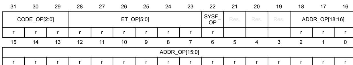
| 31 | 30 | 29 | 28 | 27 | 26 | 25 | 24 | 23 | 22 | 21 | 20 | 19 | 18 | 17 | 16 | |
| CODE_OP[2:0] | ET_OP[5:0] | SYSF_OP | Res. | Res. | Res. | ADDR_OP[18:16] | ||||||||||
| r | r | r | r | r | r | r | r | r | r | r | r | r | ||||
| 15 | 14 | 13 | 12 | 11 | 10 | 9 | 8 | 7 | 6 | 5 | 4 | 3 | 2 | 1 | 0 | |
| ADDR_OP[15:0] | ||||||||||||||||
| r | r | r | r | r | r | r | r | r | r | r | r | r | r | r | r | |
Bits 31:29 CODE_OP[2:0] : Flash memory operation code
This field indicates which flash memory operation has been interrupted:
000: No flash operation interrupted
001: Single write operation interrupted
010: Burst write operation interrupted
011: Page erase operation interrupted
100: Reserved
101: Mass erase operation interrupted
110: Option change operation interrupted
111: Reserved
Bits 28:23 ET_OP[5:0] : Elapsed erase time or burst programmed double-words before interruption
On an erase interruption, this field indicates the elapsed erase time before interruption with a 500 µs resolution.
On a burst programming interruption, this field indicates the number of correctly programmed double-words before interruption.
Bit 22 SYSF_OP : Operation in system flash memory interrupted
This bit indicates that an interruption occurred during an operation in the system flash memory.
Bits 21:19 Reserved, must be kept at reset value.
Bits 18:0 ADDR_OP[18:0] : Interrupted operation address
This field indicates which address in the flash memory was accessed when an interruption occurred. The address is given relative to the flash base address, from offset 0x0 0000 to 0x7 FFF8.
7.9.12 FLASH control 2 register (FLASH_NSCR2)
Address offset: 0x038
Reset value: 0x0000 0000
Access: no wait state; word, half-word, and byte access
This register is nonsecure. It can be read and written by both secure and nonsecure access. This register can be protected against unprivileged access when NSPRIV = 1 in the FLASH_PRIVCFGR register.
| 31 | 30 | 29 | 28 | 27 | 26 | 25 | 24 | 23 | 22 | 21 | 20 | 19 | 18 | 17 | 16 |
|---|---|---|---|---|---|---|---|---|---|---|---|---|---|---|---|
| Res. | Res. | Res. | Res. | Res. | Res. | Res. | Res. | Res. | Res. | Res. | Res. | Res. | Res. | Res. | Res. |
| 15 | 14 | 13 | 12 | 11 | 10 | 9 | 8 | 7 | 6 | 5 | 4 | 3 | 2 | 1 | 0 |
| Res. | Res. | Res. | Res. | Res. | Res. | Res. | OPA | Res. | Res. | Res. | Res. | Res. | Res. | ES | PS |
| rs | rw | rw |
Bits 31:9 Reserved, must be kept at reset value.
Bit 8 OPA : Flash operation abort
This register bit can be set by software or hardware, and is cleared by hardware.
This register bit is software write protected with LOCK and must be unlocked by NSKEY unlock. Hardware can set this bit regardless LOCK.
0: no effect
1: writing 1 when a flash nonsecure operation is ongoing will abort the ongoing flash nonsecure operation.
Note: writing 1 when no flash operation is ongoing is ignored.
Bits 7:2 Reserved, must be kept at reset value.
Bit 1 ES : Erase suspend request
0: erase suspend disabled
1: erase suspend requested (enabled)
Bit 0 PS : Program suspend request
0: program suspend disabled
1: program suspend requested (enabled)
7.9.13 FLASH secure control 2 register (FLASH_SECCR2)
Address offset: 0x03C
Reset value: 0x0000 0000
Access: no wait state; word, half-word, and byte access
This register is secure. It can be read and written only by secure access. A nonsecure read/write access is RAZ/WI. This register can be protected against unprivileged access when SPRIV = 1 in the FLASH_PRIVCFGR register.
| 31 | 30 | 29 | 28 | 27 | 26 | 25 | 24 | 23 | 22 | 21 | 20 | 19 | 18 | 17 | 16 |
|---|---|---|---|---|---|---|---|---|---|---|---|---|---|---|---|
| Res. | Res. | Res. | Res. | Res. | Res. | Res. | Res. | Res. | Res. | Res. | Res. | Res. | Res. | Res. | Res. |
| 15 | 14 | 13 | 12 | 11 | 10 | 9 | 8 | 7 | 6 | 5 | 4 | 3 | 2 | 1 | 0 |
| Res. | Res. | Res. | Res. | Res. | Res. | Res. | OPA | Res. | Res. | Res. | Res. | Res. | Res. | ES | PS |
| rs | rw | rw |
Bits 31:9 Reserved, must be kept at reset value.
Bit 8 OPA : Flash operation abort
This register bit can be set by software or hardware, and is cleared by hardware.
This register bit is software write protected with LOCK and must be unlocked by NSKEY unlock. Hardware can set this bit regardless LOCK.
0: no effect
1: writing 1 when a flash secure or nonsecure operation is ongoing will abort the ongoing secure or nonsecure flash operation.
Note: writing 1 when no flash operation is ongoing is ignored.
Bits 7:2 Reserved, must be kept at reset value.
Bit 1 ES : Erase suspend request
0: erase suspend disabled
1: erase suspend requested (enabled)
Bit 0 PS : Program suspend request
0: program suspend disabled
1: program suspend requested (enabled)
7.9.14 FLASH option register (FLASH_OPTR)
Address offset: 0x040
ST factory programmed value: 0x1FFF F8AA
Reset value: 0xXXXX XXXX
Register bits 0 to 31 are loaded with values from the flash memory at OBL.
Access: no wait state when no option bytes modification is ongoing; word, half-word, and byte access
This register is nonsecure. It can be read and written by both secure and nonsecure access. This register can be protected against unprivileged access when NSPRIV = 1 in the FLASH_PRIVCFGR register.
| 31 | 30 | 29 | 28 | 27 | 26 | 25 | 24 | 23 | 22 | 21 | 20 | 19 | 18 | 17 | 16 |
|---|---|---|---|---|---|---|---|---|---|---|---|---|---|---|---|
| TZEN | Res. | Res. | Res. | NBOOT0 | NSWB OOT0 | SRAM2 _RST | SRAM2 _PE | Res. | Res. | Res. | Res. | Res. | IWDG_ STDBY | IWDG_ STOP | IWDG_ SW |
| rw | rw | rw | rw | rw | rw | rw | rw |
| 15 | 14 | 13 | 12 | 11 | 10 | 9 | 8 | 7 | 6 | 5 | 4 | 3 | 2 | 1 | 0 |
|---|---|---|---|---|---|---|---|---|---|---|---|---|---|---|---|
| SRAM1 _RST | Res. | NRST_ STDBY | NRST_ STOP | Res. | BOR_LEV[2:0] | RDP[7:0] | |||||||||
| rw | rw | rw | rw | rw | rw | rw | rw | rw | rw | rw | rw | rw | rw | ||
Bit 31 TZEN : Global TrustZone security enable
0: Global TrustZone security disabled
1: Global TrustZone security enabled
Bits 30:28 Reserved, must be kept at reset value.
Bit 27 NBOOT0 : NBOOT0 option bit
0: NBOOT0 = 0
1: NBOOT0 = 1
Bit 26 NSWBBOOT0 : Software BOOT0
0: BOOT0 taken from the option bit NBOOT0
1: BOOT0 taken from PH3/BOOT0 pin
Bit 25 SRAM2_RST : SRAM2 erase upon system reset
0: SRAM2 erased when a system reset occurs
1: SRAM2 not erased when a system reset occurs
Bit 24 SRAM2_PE : SRAM2 parity check disable
0: SRAM2 parity check enabled
1: SRAM2 parity check disabled
Bits 23:19 Reserved, must be kept at reset value.
Bit 18 IWDG_STDBY : Independent watchdog counter freeze in Standby mode
0: Independent watchdog counter frozen in Standby mode
1: Independent watchdog counter running in Standby mode
Bit 17 IWDG_STOP : Independent watchdog counter freeze in Stop mode
0: Independent watchdog counter frozen in Stop mode
1: Independent watchdog counter running in Stop mode
Bit 16 IWDG_SW : Independent watchdog enable selection
0: Hardware mode, independent watchdog started automatically by hardware on reset selected
1: Software mode, independent watchdog started by software command selected
Bit 15 SRAM1_RST : SRAM1 erase upon system reset
0: SRAM1 erased when a system reset occurs
1: SRAM1 not erased when a system reset occurs
Bit 14 Reserved, must be kept at reset value.
Bit 13 NRST_STDBY : Reset generation in Standby mode
0: Reset generated when entering the Standby mode
1: No reset generated when entering the Standby mode
Bit 12
NRST_STOP
: Reset generation in Stop mode
0: Reset generated when entering the Stop mode
1: No reset generated when entering the Stop mode
Bit 11 Reserved, must be kept at reset value.
Bits 10:8
BOR_LEV[2:0]
: BOR reset level
These bits contain the
\(
V_{DD}
\)
supply level threshold that activates/releases the reset.
000: BOR level 0 (reset level threshold around 1.7 V)
001: BOR level 1 (reset level threshold around 2.0 V)
010: BOR level 2 (reset level threshold around 2.2 V)
011: BOR level 3 (reset level threshold around 2.5 V)
100: BOR level 4 (reset level threshold around 2.8 V)
Bits 7:0
RDP[7:0]
: Readout protection level
0xAA: Level 0 (readout protection not active)
0x55: Level 0.5 (readout protection not active, only nonsecure debug access is possible). Only available when TrustZone is active (TZEN=1)
0xCC: Level 2 (chip readout protection active)
Others: Level 1 (memories readout protection active)
Note: Refer to Section 7.6.2 for more details.
7.9.15 FLASH boot address 0 register (FLASH_NSBOOTADD0R)
Address offset: 0x044
ST factory programmed value: 0x0800 007F
Reset value: 0xXXXX XXXX
The option bytes are loaded with values from the flash memory at reset release.
Access: no wait state when no option bytes modification is ongoing; word, half-word, and byte access
This register is nonsecure. It can be read and written by both secure and nonsecure access. This register can be protected against unprivileged access when NSPRIV = 1 in the FLASH_PRIVCFG register.
| 31 | 30 | 29 | 28 | 27 | 26 | 25 | 24 | 23 | 22 | 21 | 20 | 19 | 18 | 17 | 16 |
| NSBOOTADD0[24:9] | |||||||||||||||
| rw | rw | rw | rw | rw | rw | rw | rw | rw | rw | rw | rw | rw | rw | rw | rw |
| 15 | 14 | 13 | 12 | 11 | 10 | 9 | 8 | 7 | 6 | 5 | 4 | 3 | 2 | 1 | 0 |
| NSBOOTADD0[8:0] | Res. | Res. | Res. | Res. | Res. | Res. | Res. | ||||||||
| rw | rw | rw | rw | rw | rw | rw | rw | rw | |||||||
Bits 31:7 NSBOOTADD0[24:0] : Nonsecure boot base address 0
The nonsecure boot memory address can be programmed to any address in the valid address range (see Table 8: Boot space versus RDP protection ) with a granularity of 128 bytes. These bits correspond to address [31:7]. The NSBOOTADD0 option bytes are selected following the BOOT0 pin or NSWBOOT0 state.
Examples:
NSBOOTADD0[24:0] = 0x0100000: Boot from flash memory (0x0800 0000)
NSBOOTADD0[24:0] = 0x017F100: Boot from system memory bootloader (0x0BF8 8000)
NSBOOTADD0[24:0] = 0x0400200: Boot from SRAM2 on S-Bus (0x2001 0000)
Bits 6:0 Reserved, must be kept at reset value.
7.9.16 FLASH boot address 1 register (FLASH_NSBOOTADD1R)
Address offset: 0x048
ST factory programmed value: 0x0BF8 F07F
Reset value: 0xXXXX XXXX
The option bytes are loaded with values from the flash memory at reset release.
Access: no wait state when no option bytes modification is ongoing; word, half-word, and byte access
This register is nonsecure. It can be read and written by both secure and nonsecure access. This register can be protected against unprivileged access when NSPRIV = 1 in the FLASH_PRIVCFGR register.
| 31 | 30 | 29 | 28 | 27 | 26 | 25 | 24 | 23 | 22 | 21 | 20 | 19 | 18 | 17 | 16 |
| NSBOOTADD1[24:9] | |||||||||||||||
| rw | rw | rw | rw | rw | rw | rw | rw | rw | rw | rw | rw | rw | rw | rw | rw |
| 15 | 14 | 13 | 12 | 11 | 10 | 9 | 8 | 7 | 6 | 5 | 4 | 3 | 2 | 1 | 0 |
| NSBOOTADD1[8:0] | Res | Res | Res | Res | Res | Res | Res | ||||||||
| rw | rw | rw | rw | rw | rw | rw | rw | rw | |||||||
Bits 31:7 NSBOOTADD1[24:0] : Nonsecure boot address 1
The nonsecure boot memory address can be programmed to any address in the valid address range (see Table 8: Boot space versus RDP protection ) with a granularity of 128 bytes. These bits correspond to address [31:7]. The NSBOOTADD0 option bytes are selected following the BOOT0 pin or NSWBOOT0 state.
Examples:
NSBOOTADD1[24:0] = 0x0100000: boot from flash memory (0x0800 0000)
NSBOOTADD1[24:0] = 0x017F100: boot from system memory bootloader (0x0BF8 8000)
NSBOOTADD1[24:0] = 0x0400200: boot from SRAM2 (0x2001 0000)
Bits 6:0 Reserved, must be kept at reset value.
7.9.17 FLASH secure boot address 0 register (FLASH_SECBOOTADD0R)
Address offset: 0x04C
ST factory programmed value: 0x0C00 007C
Reset value: 0xXXXX XXXX
The option bytes are loaded with values from the flash memory at reset release.
Access: no wait state when no option bytes modification is ongoing; word, half-word, and byte access
This register is secure. It can be read and written only by secure access. A nonsecure read/write access is RAZ/WI. This register can be protected against unprivileged access when SPRIV = 1 in the FLASH_PRIVCFG register.
| 31 | 30 | 29 | 28 | 27 | 26 | 25 | 24 | 23 | 22 | 21 | 20 | 19 | 18 | 17 | 16 |
| SECBOOTADD0[24:9] | |||||||||||||||
| rw | rw | rw | rw | rw | rw | rw | rw | rw | rw | rw | rw | rw | rw | rw | rw |
| 15 | 14 | 13 | 12 | 11 | 10 | 9 | 8 | 7 | 6 | 5 | 4 | 3 | 2 | 1 | 0 |
| SECBOOTADD0[8:0] | Res. | Res. | Res. | Res. | Res. | BOOT_LOCK | |||||||||
| rw | rw | rw | rw | rw | rw | rw | rw | rw | rs | ||||||
Bits 31:7 SECBOOTADD0[24:0] : Secure boot base address 0
This address is only used when TZEN = 1.
The secure boot memory address can be programmed to any address in the valid address range (see Table 8: Boot space versus RDP protection ) with a granularity of 128 bytes. This bits correspond to address [31:7] The SECBOOTADD0 option bytes are selected following the BOOT0 pin or NSWBOOT0 state.
Examples:
SECBOOTADD0[24:0] = 0x018 0000: Boot from secure user flash memory (0x0C00 0000)
SECBOOTADD0[24:0] = 0x01F F000: Boot from RSS system flash memory (0x0FF8 0000)
SECBOOTADD0[24:0] = 0x060 0000: Boot from secure SRAM1 on S-Bus (0x3000 0000)
Bits 6:1 Reserved, must be kept at reset value.
Bit 0 BOOT_LOCK : Boot lock
This lock is only used when TZEN = 1.
When set, the boot is always forced to base address value programmed in SECBOOTADD0[24:0] option bytes whatever the boot selection option. When set, this bit can only be cleared by an RDP regression level 1 to level 0.
7.9.18 FLASH secure watermark register 1 (FLASH_SECWMR1)
Address offset: 0x050
ST factory programmed value: 0xFFFF FF80
Reset value: 0xXXXX XXXX
Register bits are loaded with values from the flash memory at OBL. Reserved bits are read as 1.
Access: no wait state when no option bytes modification is ongoing; word, half-word, and byte access
This register is secure. It can be read and written only by secure access. A nonsecure read/write access is RAZ/WI. This register can be protected against unprivileged access when SPRIV = 1 in the FLASH_PRIVCFG register.
| 31 | 30 | 29 | 28 | 27 | 26 | 25 | 24 | 23 | 22 | 21 | 20 | 19 | 18 | 17 | 16 |
| Res. | Res. | Res. | Res. | Res. | Res. | Res. | Res. | Res. | SECWM_PEND[6:0] | ||||||
| rw | rw | rw | rw | rw | rw | rw | |||||||||
| 15 | 14 | 13 | 12 | 11 | 10 | 9 | 8 | 7 | 6 | 5 | 4 | 3 | 2 | 1 | 0 |
| Res. | Res. | Res. | Res. | Res. | Res. | Res. | Res. | Res. | SECWM_PSTRT[6:0] | ||||||
| rw | rw | rw | rw | rw | rw | rw | |||||||||
Bits 31:23 Reserved, must be kept at reset value.
Bits 22:16 SECWM_PEND[6:0] : End page of secure area
This field contains the last page of the secure area.
Bits 15:7 Reserved, must be kept at reset value.
Bits 6:0 SECWM_PSTRT[6:0] : Start page of secure area
This field contains the first page of the secure area.
7.9.19 FLASH secure watermark register 2 (FLASH_SECWMR2)
Address offset: 0x054
ST factory programmed value: 0xB480 FFFF
Reset value: 0xXXXX XXXX
Register bits are loaded with values from the flash memory at OBL.
Access: no wait state when no option bytes modification is ongoing; word, half-word, and byte access
This register is secure, it can be read and written only by secure access. A nonsecure read/write access is RAZ/WI. This register can be protected against unprivileged access when SPRIV = 1 in the FLASH_PRIVCFG register.
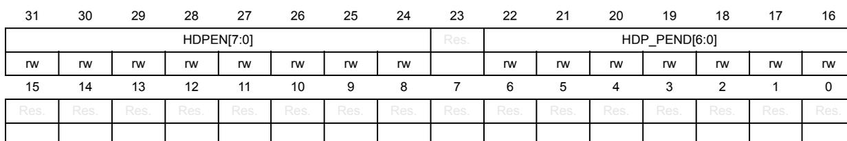
| 31 | 30 | 29 | 28 | 27 | 26 | 25 | 24 | 23 | 22 | 21 | 20 | 19 | 18 | 17 | 16 |
| HDPEN[7:0] | Res. | HDP_PEND[6:0] | |||||||||||||
| rw | rw | rw | rw | rw | rw | rw | rw | rw | rw | rw | rw | rw | rw | rw | |
| 15 | 14 | 13 | 12 | 11 | 10 | 9 | 8 | 7 | 6 | 5 | 4 | 3 | 2 | 1 | 0 |
| Res. | Res. | Res. | Res. | Res. | Res. | Res. | Res. | Res. | Res. | Res. | Res. | Res. | Res. | Res. | Res. |
Bits 31:24 HDPEN[7:0] : Secure Hide protection area enable
0xB4: No secure HDP area
others: Secure HDP area enabled
Bit 23 Reserved, must be kept at reset value.
Bits 22:16 HDP_PEND[6:0] : End page of secure hide protection area
This field contains the last page of the secure HDP area.
Bits 15:0 Reserved, must be kept at reset value.
7.9.20 FLASH WRP area A address register (FLASH_WRPAR)
Address offset: 0x058
ST factory programmed value: 0xFF80 FFFF
Reset value: 0xXXXX XXXX
Register bits are loaded with values from the flash memory at OBL. Reserved bits are read as 1.
Access: no wait state when no option bytes modification is ongoing; word, half-word, and byte access
This register is nonsecure. It can be read and written by both secure and nonsecure access.
This register can be protected against unprivileged access when NSPRIV = 1 in the FLASH_PRIVCFG register.
| 31 | 30 | 29 | 28 | 27 | 26 | 25 | 24 | 23 | 22 | 21 | 20 | 19 | 18 | 17 | 16 |
|---|---|---|---|---|---|---|---|---|---|---|---|---|---|---|---|
| UNLOCK | Res. | Res. | Res. | Res. | Res. | Res. | Res. | Res. | WRPA_PEND[6:0] | ||||||
| rw | rw | rw | rw | rw | rw | rw | rw | ||||||||
| 15 | 14 | 13 | 12 | 11 | 10 | 9 | 8 | 7 | 6 | 5 | 4 | 3 | 2 | 1 | 0 |
| Res. | Res. | Res. | Res. | Res. | Res. | Res. | Res. | Res. | WRPA_PSTRT[6:0] | ||||||
| rw | rw | rw | rw | rw | rw | rw | |||||||||
Bit 31 UNLOCK : WPR area A unlock
0: WRPA start and end pages locked
1: WRPA start and end pages unlocked
Bits 30:23 Reserved, must be kept at reset value.
Bits 22:16 WRPA_PEND[6:0] : WPR area A end page
This field contains the last page of the WPR area A.
Bits 15:7 Reserved, must be kept at reset value.
Bits 6:0 WRPA_PSTRT[6:0] : WPR area A start page
This field contains the first page of the WPR area A.
7.9.21 FLASH WRP area B address register (FLASH_WRPBR)
Address offset: 0x05C
ST factory programmed value: 0xFF80 FFFF
Reset value: 0xXXXX XXXX
Register bits are loaded with values from the flash memory at OBL.
Access: no wait state when no option bytes modification is ongoing; word, half-word, and byte access
This register is nonsecure. It can be read and written by both secure and nonsecure access.
This register can be protected against unprivileged access when NSPRIV = 1 in the FLASH_PRIVCFG register.
| 31 | 30 | 29 | 28 | 27 | 26 | 25 | 24 | 23 | 22 | 21 | 20 | 19 | 18 | 17 | 16 |
|---|---|---|---|---|---|---|---|---|---|---|---|---|---|---|---|
| UNLOCK | Res. | Res. | Res. | Res. | Res. | Res. | Res. | Res. | WRPB_PEND[6:0] | ||||||
| rw | rw | rw | rw | rw | rw | rw | rw | ||||||||
| 15 | 14 | 13 | 12 | 11 | 10 | 9 | 8 | 7 | 6 | 5 | 4 | 3 | 2 | 1 | 0 |
| Res. | Res. | Res. | Res. | Res. | Res. | Res. | Res. | Res. | WRPB_PSTRT[6:0] | ||||||
| rw | rw | rw | rw | rw | rw | rw | |||||||||
Bit 31 UNLOCK : WPR area B unlock
0: WRPB start and end pages locked
1: WRPB start and end pages unlocked
Bits 30:23 Reserved, must be kept at reset value.
Bits 22:16 WRPB_PEND[6:0] : WRP area B end page
This field contains the last page of the WRP area B.
Bits 15:7 Reserved, must be kept at reset value.
Bits 6:0 WRPB_PSTRT[6:0] : WRP area B start page
This field contains the first page of the WRP area B.
7.9.22 FLASH secure block based register x (FLASH_SECBBRx)
Address offset: \( 0x080 + 0x4 \times (x - 1) \) , ( \( x = 1 \) to 4)
Reset value: 0x0000 0000
Access: no wait state; word, half-word, and byte access
This register is secure. It can be written only by secure access. Individual register bits can be protected against unprivileged access (refer to Table 69 ).
| 31 | 30 | 29 | 28 | 27 | 26 | 25 | 24 | 23 | 22 | 21 | 20 | 19 | 18 | 17 | 16 |
|---|---|---|---|---|---|---|---|---|---|---|---|---|---|---|---|
| SECBB 31 | SECBB 30 | SECBB 29 | SECBB 28 | SECBB 27 | SECBB 26 | SECBB 25 | SECBB 24 | SECBB 23 | SECBB 22 | SECBB 21 | SECBB 20 | SECBB 19 | SECBB 18 | SECBB 17 | SECBB 16 |
| rw | rw | rw | rw | rw | rw | rw | rw | rw | rw | rw | rw | rw | rw | rw | rw |
| 15 | 14 | 13 | 12 | 11 | 10 | 9 | 8 | 7 | 6 | 5 | 4 | 3 | 2 | 1 | 0 |
| SECBB 15 | SECBB 14 | SECBB 13 | SECBB 12 | SECBB 11 | SECBB 10 | SECBB 9 | SECBB 8 | SECBB 7 | SECBB 6 | SECBB 5 | SECBB 4 | SECBB 3 | SECBB 2 | SECBB 1 | SECBB 0 |
| rw | rw | rw | rw | rw | rw | rw | rw | rw | rw | rw | rw | rw | rw | rw | rw |
Bits 31:0 SECBB[31:0] : page secure/nonsecure attribution ( \( y = 0 \) to 31)
Each bit is used to set one page security attribution.
0: Page \( (32 \times (x - 1) + y) \) in flash not block-based secure
1: Page \( (32 \times (x - 1) + y) \) in flash block-based secure
7.9.23 FLASH secure HDP control register (FLASH_SECHDPCR)
Address offset: 0x0C0
Reset value: 0x00A3 00A3
Access: no wait state; word, half-word, and byte access
This register is secure. It can be read and written only by secure access. A nonsecure read/write access is RAZ/WI. This register can be protected against unprivileged access when SPRIV = 1 in the FLASH_PRIVCFGR register.
| 31 | 30 | 29 | 28 | 27 | 26 | 25 | 24 | 23 | 22 | 21 | 20 | 19 | 18 | 17 | 16 |
|---|---|---|---|---|---|---|---|---|---|---|---|---|---|---|---|
| Res. | Res. | Res. | Res. | Res. | Res. | Res. | Res. | HDPEXT_ACCDIS[7:0] | |||||||
| rw | rw | rw | rw | rw | rw | rw | rw | ||||||||
| 15 | 14 | 13 | 12 | 11 | 10 | 9 | 8 | 7 | 6 | 5 | 4 | 3 | 2 | 1 | 0 |
| Res. | Res. | Res. | Res. | Res. | Res. | Res. | Res. | HDP_ACCDIS[7:0] | |||||||
| rw | rw | rw | rw | rw | rw | rw | rw | ||||||||
Bits 31:24 Reserved, must be kept at reset value.
Bits 23:16 HDPPEXT_ACCDIS[7:0] : Secure HDP extension area access disable
When set to a value different than 0xA3, these bit can't be modified anymore, except by a system reset or standby reset.
0xA3: Access to secure HDP extension area granted
0x5C: Access to secure HDP area and HDP extension area denied, and HDP_PEXT increment allowed at any time. SECWMRx option bytes modification blocked.
other: Access to secure HDP area, HDP extension area, and HDP_PEXT denied. SECWMRx option bytes modification blocked.
(refer to Rules for modifying specific option bytes )
Bits 15:8 Reserved, must be kept at reset value.
Bits 7:0 HDP_ACCDIS[7:0] : Secure HDP area access disable
When set to a value different than 0xA3, these bit can't be modified anymore, except by a system reset or standby reset.
0xA3: Access to secure HDP area granted
other: Access to secure HDP area denied. SECWMRx option bytes modification blocked.
(refer to Rules for modifying specific option bytes )
7.9.24 FLASH privilege configuration register (FLASH_PRIFCFGR)
Address offset: 0x0C4
Reset value: 0x0000 0000
Access: no wait state; word, half-word, and byte access
This register is privileged write protected. It can be written only by a privileged access. All bits in this register can be read by both privileged and unprivileged, secure and nonsecure access.
| 31 | 30 | 29 | 28 | 27 | 26 | 25 | 24 | 23 | 22 | 21 | 20 | 19 | 18 | 17 | 16 |
|---|---|---|---|---|---|---|---|---|---|---|---|---|---|---|---|
| Res. | Res. | Res. | Res. | Res. | Res. | Res. | Res. | Res. | Res. | Res. | Res. | Res. | Res. | Res. | Res. |
| 15 | 14 | 13 | 12 | 11 | 10 | 9 | 8 | 7 | 6 | 5 | 4 | 3 | 2 | 1 | 0 |
| Res. | Res. | Res. | Res. | Res. | Res. | Res. | Res. | Res. | Res. | Res. | Res. | Res. | Res. | NSPRIV V | SPRIV |
| rw | rw |
Bits 31:2 Reserved, must be kept at reset value.
Bit 1 NSPRIV : Privileged protection for nonsecure registers
0: Nonsecure flash registers can be read and written by privileged or unprivileged access.
1: Nonsecure flash registers can be read and written by privileged access only.
Bit 0 SPRIV : Privileged protection for secure registers
This bit is secure write protected. It can only be written by a secure privileged access when TrustZone is enabled (TZEN = 1).
0: Secure flash registers can be read and written by privileged or unprivileged access.
1: Secure flash registers can be read and written by privileged access only.
7.9.25 FLASH secure HDP extension register (FLASH_SECHDPEXTR)
Address offset: 0x0C8
Reset value: 0x0000 0000
Access: no wait state; word, half-word, and byte access
This register is secure. It can be read and written only by secure access. A nonsecure read/write access is RAZ/WI. This register can be protected against unprivileged access when SPRIV = 1 in the FLASH_PRIVCFGR register.
| 31 | 30 | 29 | 28 | 27 | 26 | 25 | 24 | 23 | 22 | 21 | 20 | 19 | 18 | 17 | 16 |
|---|---|---|---|---|---|---|---|---|---|---|---|---|---|---|---|
| Res. | Res. | Res. | Res. | Res. | Res. | Res. | Res. | Res. | Res. | Res. | Res. | Res. | Res. | Res. | Res. |
| 15 | 14 | 13 | 12 | 11 | 10 | 9 | 8 | 7 | 6 | 5 | 4 | 3 | 2 | 1 | 0 |
| Res. | Res. | Res. | Res. | Res. | Res. | Res. | Res. | Res. | HDP_PEXT[6:0] | ||||||
| rw | rw | rw | rw | rw | rw | rw | |||||||||
Bits 31:7 Reserved, must be kept at reset value.
Bits 6:0 HDP_PEXT[6:0] : Number of secure HDP extension area pages.
This field contains the number of flash pages assigned to the HDP extension area.
When HDPEN is enabled, the HDP extension area starts at HDP_PEND + 1.
When HDPEN is disabled the HDP extension area starts at SECWM_PSTART.
7.9.26 FLASH privilege block based register x (FLASH_PRIVBBRx)
Address offset: 0x0D0 + 0x4 * (x - 1), (x = 1 to 4)
Reset value: 0x0000 0000
Access: no wait state; word, half-word, and byte access
This register is privileged. It can be read written only by a privileged access. Individual register bits can be protected against nonsecure access (refer to Table 69 ).
| 31 | 30 | 29 | 28 | 27 | 26 | 25 | 24 | 23 | 22 | 21 | 20 | 19 | 18 | 17 | 16 |
|---|---|---|---|---|---|---|---|---|---|---|---|---|---|---|---|
| PRIVB B31 | PRIVB B30 | PRIVB B29 | PRIVB B28 | PRIVB B27 | PRIVB B26 | PRIVB B25 | PRIVB B24 | PRIVB B23 | PRIVB B22 | PRIVB B21 | PRIVB B20 | PRIVB B19 | PRIVB B18 | PRIVB B17 | PRIVB B16 |
| rw | rw | rw | rw | rw | rw | rw | rw | rw | rw | rw | rw | rw | rw | rw | rw |
| 15 | 14 | 13 | 12 | 11 | 10 | 9 | 8 | 7 | 6 | 5 | 4 | 3 | 2 | 1 | 0 |
| PRIVB B15 | PRIVB B14 | PRIVB B13 | PRIVB B12 | PRIVB B11 | PRIVB B10 | PRIVB B9 | PRIVB B8 | PRIVB B7 | PRIVB B6 | PRIVB B5 | PRIVB B4 | PRIVB B3 | PRIVB B2 | PRIVB B1 | PRIVB B0 |
| rw | rw | rw | rw | rw | rw | rw | rw | rw | rw | rw | rw | rw | rw | rw | rw |
Bits 31:0 PRIVBB[31:0] : page privileged/unprivileged attribution (y = 0 to 31)
Each bit is used to set one page privilege attribution in flash.
0: Page (32 x (x - 1) + y) in flash accessible by unprivileged access
1: Page (32 x (x - 1) + y) in flash only accessible by privileged access
7.9.27 FLASH OEM1 key register 1 (FLASH_OEM1KEYR1)
Address offset: 0x110
ST factory programmed value: 0xFFFF FFFF
Reset value: 0x0000 0000
Access: no wait state when no option bytes modification is ongoing; word, half-word, and byte access
This register is nonsecure. It can be written by both secure and nonsecure access. This register is read as zero. This register can be protected against unprivileged access when NSPRIV = 1 in the FLASH_PRIVCFG register.

| 31 | 30 | 29 | 28 | 27 | 26 | 25 | 24 | 23 | 22 | 21 | 20 | 19 | 18 | 17 | 16 |
| OEM1KEY[31:16] | |||||||||||||||
| w | w | w | w | w | w | w | w | w | w | w | w | w | w | w | w |
| 15 | 14 | 13 | 12 | 11 | 10 | 9 | 8 | 7 | 6 | 5 | 4 | 3 | 2 | 1 | 0 |
| OEM1KEY[15:0] | |||||||||||||||
| w | w | w | w | w | w | w | w | w | w | w | w | w | w | w | w |
Bits 31:0 OEM1KEY[31:0] : OEM1 key least significant bytes
7.9.28 FLASH OEM1 key register 2 (FLASH_OEM1KEYR2)
Address offset: 0x114
ST factory programmed value: 0xFFFF FFFF
Reset value: 0xXXXX XXXX
Access: no wait state when no option bytes modification is ongoing; word, half-word, and byte access
This register is nonsecure. It can be written by both secure and nonsecure access. This register is read as zero. This register can be protected against unprivileged access when NSPRIV = 1 in the FLASH_PRIVCFG register.

| 31 | 30 | 29 | 28 | 27 | 26 | 25 | 24 | 23 | 22 | 21 | 20 | 19 | 18 | 17 | 16 |
| OEM1KEY[63:48] | |||||||||||||||
| w | w | w | w | w | w | w | w | w | w | w | w | w | w | w | w |
| 15 | 14 | 13 | 12 | 11 | 10 | 9 | 8 | 7 | 6 | 5 | 4 | 3 | 2 | 1 | 0 |
| OEM1KEY[47:32] | |||||||||||||||
| w | w | w | w | w | w | w | w | w | w | w | w | w | w | w | w |
Bits 31:0 OEM1KEY[63:32] : OEM1 key middle bytes
7.9.29 FLASH OEM1 key register 3 (FLASH_OEM1KEYR3)
Address offset: 0x118
ST factory programmed value: 0xFFFF FFFF
Reset value: 0xXXXX XXXX
Access: no wait state when no option bytes modification is ongoing; word, half-word, and byte access
This register is nonsecure. It can be written by both secure and nonsecure access. This register is read as zero. This register can be protected against unprivileged access when NSPRIV = 1 in the FLASH_PRIVCFG register.

| 31 | 30 | 29 | 28 | 27 | 26 | 25 | 24 | 23 | 22 | 21 | 20 | 19 | 18 | 17 | 16 |
| OEM1KEY[95:80] | |||||||||||||||
| w | w | w | w | w | w | w | w | w | w | w | w | w | w | w | w |
| 15 | 14 | 13 | 12 | 11 | 10 | 9 | 8 | 7 | 6 | 5 | 4 | 3 | 2 | 1 | 0 |
| OEM1KEY[79:64] | |||||||||||||||
| w | w | w | w | w | w | w | w | w | w | w | w | w | w | w | w |
Bits 31:0 OEM1KEY[95:64] : OEM1 key middle bytes
7.9.30 FLASH OEM1 key register 4 (FLASH_OEM1KEYR4)
Address offset: 0x11C
ST factory programmed value: 0xFFFF FFFF
Reset value: 0xXXXX XXXX
Access: no wait state when no option bytes modification is ongoing; word, half-word, and byte access
This register is nonsecure. It can be written by both secure and nonsecure access. This register is read as zero. This register can be protected against unprivileged access when NSPRIV = 1 in the FLASH_PRIVCFG register.

| 31 | 30 | 29 | 28 | 27 | 26 | 25 | 24 | 23 | 22 | 21 | 20 | 19 | 18 | 17 | 16 |
| OEM1KEY[127:112] | |||||||||||||||
| w | w | w | w | w | w | w | w | w | w | w | w | w | w | w | w |
| 15 | 14 | 13 | 12 | 11 | 10 | 9 | 8 | 7 | 6 | 5 | 4 | 3 | 2 | 1 | 0 |
| OEM1KEY[111:96] | |||||||||||||||
| w | w | w | w | w | w | w | w | w | w | w | w | w | w | w | w |
Bits 31:0 OEM1KEY[127:96] : OEM1 key most significant bytes
7.9.31 FLASH OEM2 key register 1 (FLASH_OEM2KEYR1)
Address offset: 0x120
ST factory programmed value: 0xFFFF FFFF
Reset value: 0xXXXX XXXX
Access: no wait state when no option bytes modification is ongoing; word, half-word, and byte access
This register is nonsecure. It can be written by both secure and nonsecure access. This register is read as zero. This register can be protected against unprivileged access when NSPRIV = 1 in the FLASH_PRIVCFG register.
| 31 | 30 | 29 | 28 | 27 | 26 | 25 | 24 | 23 | 22 | 21 | 20 | 19 | 18 | 17 | 16 |
| OEM2KEY[31:16] | |||||||||||||||
| w | w | w | w | w | w | w | w | w | w | w | w | w | w | w | w |
| 15 | 14 | 13 | 12 | 11 | 10 | 9 | 8 | 7 | 6 | 5 | 4 | 3 | 2 | 1 | 0 |
| OEM2KEY[15:0] | |||||||||||||||
| w | w | w | w | w | w | w | w | w | w | w | w | w | w | w | w |
Bits 31:0 OEM2KEY[31:0] : OEM2 key least significant bytes
7.9.32 FLASH OEM2 key register 2 (FLASH_OEM2KEYR2)
Address offset: 0x124
ST factory programmed value: 0xFFFF FFFF
Reset value: 0xXXXX XXXX
Access: no wait state when no option bytes modification is ongoing; word, half-word, and byte access
This register is nonsecure. It can be written by both secure and nonsecure access. This register can be protected against unprivileged access when NSPRIV = 1 in the FLASH_PRIVCFG register.
| 31 | 30 | 29 | 28 | 27 | 26 | 25 | 24 | 23 | 22 | 21 | 20 | 19 | 18 | 17 | 16 |
| OEM2KEY[63:48] | |||||||||||||||
| w | w | w | w | w | w | w | w | w | w | w | w | w | w | w | w |
| 15 | 14 | 13 | 12 | 11 | 10 | 9 | 8 | 7 | 6 | 5 | 4 | 3 | 2 | 1 | 0 |
| OEM2KEY[47:32] | |||||||||||||||
| w | w | w | w | w | w | w | w | w | w | w | w | w | w | w | w |
Bits 31:0 OEM2KEY[63:32] : OEM2 key middle bytes
7.9.33 FLASH OEM2 key register 3 (FLASH_OEM2KEYR3)
Address offset: 0x128
ST factory programmed value: 0xFFFF FFFF
Reset value: 0xXXXX XXXX
Access: no wait state when no option bytes modification is ongoing; word, half-word, and byte access
This register is nonsecure. It can be written by both secure and nonsecure access. This register is read as zero. This register can be protected against unprivileged access when NSPRIV = 1 in the FLASH_PRIVCFG register.

| 31 | 30 | 29 | 28 | 27 | 26 | 25 | 24 | 23 | 22 | 21 | 20 | 19 | 18 | 17 | 16 |
| OEM2KEY[95:80] | |||||||||||||||
| w | w | w | w | w | w | w | w | w | w | w | w | w | w | w | w |
| 15 | 14 | 13 | 12 | 11 | 10 | 9 | 8 | 7 | 6 | 5 | 4 | 3 | 2 | 1 | 0 |
| OEM2KEY[79:64] | |||||||||||||||
| w | w | w | w | w | w | w | w | w | w | w | w | w | w | w | w |
Bits 31:0 OEM2KEY[95:64] : OEM2 key middle bytes
7.9.34 FLASH OEM2 key register 4 (FLASH_OEM2KEYR4)
Address offset: 0x12C
ST factory programmed value: 0xFFFF FFFF
Reset value: 0xXXXX XXXX
Access: no wait state when no option bytes modification is ongoing; word, half-word, and byte access
This register is nonsecure. It can be written by both secure and nonsecure access. This register can be protected against unprivileged access when NSPRIV = 1 in the FLASH_PRIVCFG register.

| 31 | 30 | 29 | 28 | 27 | 26 | 25 | 24 | 23 | 22 | 21 | 20 | 19 | 18 | 17 | 16 |
| OEM2KEY[127:112] | |||||||||||||||
| w | w | w | w | w | w | w | w | w | w | w | w | w | w | w | w |
| 15 | 14 | 13 | 12 | 11 | 10 | 9 | 8 | 7 | 6 | 5 | 4 | 3 | 2 | 1 | 0 |
| OEM2KEY[111:96] | |||||||||||||||
| w | w | w | w | w | w | w | w | w | w | w | w | w | w | w | w |
Bits 31:0 OEM2KEY[127:96] : OEM2 key most significant bytes
7.9.35 FLASH OEM key status register (FLASH_OEMKEYSR)
Address offset: 0x130
Reset value: 0x00XX 00XX
Access: no wait state when no option bytes modification is ongoing; word, half-word, and byte access
This register is nonsecure. It can be read by both secure and nonsecure access. This register can be protected against unprivileged access when NSPRIV = 1 in the FLASH_PRIVCFG register.
| 31 | 30 | 29 | 28 | 27 | 26 | 25 | 24 | 23 | 22 | 21 | 20 | 19 | 18 | 17 | 16 |
|---|---|---|---|---|---|---|---|---|---|---|---|---|---|---|---|
| Res. | Res. | Res. | Res. | Res. | Res. | Res. | Res. | OEM2KEYCRC[7:0] | |||||||
| r | r | r | r | r | r | r | r | ||||||||
| 15 | 14 | 13 | 12 | 11 | 10 | 9 | 8 | 7 | 6 | 5 | 4 | 3 | 2 | 1 | 0 |
| Res. | Res. | Res. | Res. | Res. | Res. | Res. | Res. | OEM1KEYCRC[7:0] | |||||||
| r | r | r | r | r | r | r | r | ||||||||
Bits 31:24 Reserved, must be kept at reset value.
Bits 23:16 OEM2KEYCRC[7:0] : OEM2 key CRC value
CRC is automatically computed by hardware when loading the OEM2 key. CRC computation is an checksum using the standard CRC-8-CCITT algorithm \( X^8 + X^2 + X + 1 \) (according the convention). Source code is available in Section 7.6.2: Readout protection (RDP) .
Bits 15:8 Reserved, must be kept at reset value.
Bits 7:0 OEM1KEYCRC[7:0] : OEM1 key CRC value
CRC is automatically computed by hardware when loading the OEM1 key. CRC computation is an checksum using the standard CRC-8-CCITT algorithm \( X^8 + X^2 + X + 1 \) (according the convention). Source code is available in Section 7.6.2: Readout protection (RDP) .
7.9.36 FLASH register map
Table 72. FLASH register map and reset values
| Offset | Register | 31 | 30 | 29 | 28 | 27 | 26 | 25 | 24 | 23 | 22 | 21 | 20 | 19 | 18 | 17 | 16 | 15 | 14 | 13 | 12 | 11 | 10 | 9 | 8 | 7 | 6 | 5 | 4 | 3 | 2 | 1 | 0 |
|---|---|---|---|---|---|---|---|---|---|---|---|---|---|---|---|---|---|---|---|---|---|---|---|---|---|---|---|---|---|---|---|---|---|
| 0x000 | FLASH_ACR | Res | Res | Res | Res | Res | Res | Res | Res | Res | Res | Res | Res | Res | Res | Res | Res | Res | SLEEP_PD | Res | PDREQ | LPM | Res | Res | PRFTEN | Res | Res | Res | Res | Res | Res | Res | LATENCY [3:0] |
| Reset value | 0 | 0 | 0 | 0 | 0 | 0 | 0 1 | ||||||||||||||||||||||||||
| 0x004 | Reserved | Reserved | |||||||||||||||||||||||||||||||
| 0x008 | FLASH_NSKEYR | NSKEY[31:0] | |||||||||||||||||||||||||||||||
| Reset value | 0 | 0 | 0 | 0 | 0 | 0 | 0 | 0 | 0 | 0 | 0 | 0 | 0 | 0 | 0 | 0 | 0 | 0 | 0 | 0 | 0 | 0 | 0 | 0 | 0 | 0 | 0 | 0 | 0 | 0 | 0 | 0 | |
| 0x00C | FLASH_SECKEYR | SECKEY[31:0] | |||||||||||||||||||||||||||||||
| Reset value | 0 | 0 | 0 | 0 | 0 | 0 | 0 | 0 | 0 | 0 | 0 | 0 | 0 | 0 | 0 | 0 | 0 | 0 | 0 | 0 | 0 | 0 | 0 | 0 | 0 | 0 | 0 | 0 | 0 | 0 | 0 | 0 | |
| 0x010 | FLASH_OPTKEYR | OPTKEY[31:0] | |||||||||||||||||||||||||||||||
| Reset value | 0 | 0 | 0 | 0 | 0 | 0 | 0 | 0 | 0 | 0 | 0 | 0 | 0 | 0 | 0 | 0 | 0 | 0 | 0 | 0 | 0 | 0 | 0 | 0 | 0 | 0 | 0 | 0 | 0 | 0 | 0 | 0 | |
| 0x014 | Reserved | Reserved | |||||||||||||||||||||||||||||||
| 0x018 | FLASH_PDKEY1R | PDKEY1[31:0] | |||||||||||||||||||||||||||||||
| Reset value | 0 | 0 | 0 | 0 | 0 | 0 | 0 | 0 | 0 | 0 | 0 | 0 | 0 | 0 | 0 | 0 | 0 | 0 | 0 | 0 | 0 | 0 | 0 | 0 | 0 | 0 | 0 | 0 | 0 | 0 | 0 | 0 | |
| 0x01C | Reserved | Reserved | |||||||||||||||||||||||||||||||
| 0x020 | FLASH_NSSR | Res | Res | Res | Res | Res | OPBRK | Res | Res | Res | Res | Res | PD | OEM2LOCK | OEM1LOCK | WDW | BSY | Res | Res | OPTWERR | Res | Res | Res | Res | Res | PGSERR | SIZERR | PGAERR | WRPERR | PROGERR | Res | OPERR | EOP |
| Reset value | 0 | 0 | X | X | X | X | 0 | 0 | 0 | 0 | 0 | 0 | 0 | 0 | |||||||||||||||||||
| 0x024 | FLASH_SECSR | Res | Res | Res | Res | Res | OPBRK | Res | Res | Res | Res | Res | Res | Res | Res | WDW | BSY | Res | Res | Res | Res | Res | Res | Res | Res | PGSERR | SIZERR | PGAERR | WRPERR | PROGERR | Res | OPERR | EOP |
| Reset value | 0 | 0 | 0 | 0 | 0 | 0 | 0 | 0 | 0 | 0 | |||||||||||||||||||||||
| 0x028 | FLASH_NSCR1 | LOCK | OPTLOCK | Res | Res | OBL_LAUNCH | Res | ERRIE | EOPIE | Res | Res | Res | Res | Res | Res | OPTSTRT | STRT | Res | BWR | Res | Res | Res | Res | PNB[6:0] | MER | PER | PG | ||||||
| Reset value | 1 | 1 | 0 | 0 | 0 | 0 | 0 | 0 | 0 0 0 0 0 0 | 0 | 0 | 0 | |||||||||||||||||||||
| 0x02C | FLASH_SECCR1 | LOCK | INV | Res | Res | Res | Res | ERRIE | EOPIE | Res | Res | Res | Res | Res | Res | STRT | Res | BWR | Res | Res | Res | Res | Res | PNB[6:0] | MER | PER | PG | ||||||
| Reset value | 1 | 0 | 0 | 0 | 0 | 0 | 0 0 0 0 0 0 | 0 | 0 | 0 | |||||||||||||||||||||||
| 0x030 | FLASH_ECCR | ECCD | ECCC | Res | Res | Res | Res | Res | ECCIE | Res | SYSECC | Res | Res | ADDR_ECC[19:0] | |||||||||||||||||||
| Reset value | 0 | 0 | 0 | 0 | 0 0 0 0 0 0 0 0 0 0 0 0 0 0 0 0 0 0 0 0 0 | ||||||||||||||||||||||||||||
| 0x034 | FLASH_OPSR | CODE_OP[2:0] | ET_OP[5:0] | SYSE_OP | Res | Res | ADDR_OP[19:0] | ||||||||||||||||||||||||||
| Reset value | X | X | X | X | X | X | X | X | X | X | X X X X X X X X X X X X X X X X X X X X X | ||||||||||||||||||||||
Table 72. FLASH register map and reset values (continued)
| Offset | Register | 31 | 30 | 29 | 28 | 27 | 26 | 25 | 24 | 23 | 22 | 21 | 20 | 19 | 18 | 17 | 16 | 15 | 14 | 13 | 12 | 11 | 10 | 9 | 8 | 7 | 6 | 5 | 4 | 3 | 2 | 1 | 0 | |
|---|---|---|---|---|---|---|---|---|---|---|---|---|---|---|---|---|---|---|---|---|---|---|---|---|---|---|---|---|---|---|---|---|---|---|
| 0x038 | FLASH_NSCR2 | Res. | Res. | Res. | Res. | Res. | Res. | Res. | Res. | Res. | Res. | Res. | Res. | Res. | Res. | Res. | Res. | Res. | Res. | Res. | Res. | Res. | Res. | Res. | OPA | Res. | Res. | Res. | Res. | Res. | Res. | ES | PS | |
| Reset value | 0 | 0 | 0 | |||||||||||||||||||||||||||||||
| 0x03C | FLASH_SECCR2 | Res. | Res. | Res. | Res. | Res. | Res. | Res. | Res. | Res. | Res. | Res. | Res. | Res. | Res. | Res. | Res. | Res. | Res. | Res. | Res. | Res. | Res. | Res. | OPA | Res. | Res. | Res. | Res. | Res. | Res. | ES | PS | |
| Reset value | 0 | 0 | 0 | |||||||||||||||||||||||||||||||
| 0x040 | FLASH_OPTR | TZEN | Res. | Res. | Res. | NBOOT0 | NSWBOOT0 | SRAM2_RST | SRAM2_PE | Res. | Res. | Res. | Res. | Res. | IWDG_STDBY | IWDG_STOP | IWDG_SW | SRAM1_RST | Res. | NRST_STDBY | NRST_STOP | Res. | Res. | BOR_LEV[2:0] | RDP[7:0] | |||||||||
| Reset value | X | X | X | X | X | X | X | X | X | X | X | X | X | X | X | X | X | X | X | X | X | |||||||||||||
| 0x044 | FLASH_NSBOOTADDR0R | NSBOOTADDR0[24:0] | Res. | Res. | Res. | Res. | Res. | Res. | Res. | |||||||||||||||||||||||||
| Reset value | X | X | X | X | X | X | X | X | X | X | X | X | X | X | X | X | X | X | X | X | X | X | X | X | X | |||||||||
| 0x048 | FLASH_NSBOOTADDR1R | NSBOOTADDR1[24:0] | Res. | Res. | Res. | Res. | Res. | Res. | Res. | |||||||||||||||||||||||||
| Reset value | X | X | X | X | X | X | X | X | X | X | X | X | X | X | X | X | X | X | X | X | X | X | X | X | X | |||||||||
| 0x04C | FLASH_SECBOOTADDR0R | SECBOOTADDR0[24:0] | Res. | Res. | Res. | Res. | Res. | Res. | BOOT_LOCK | |||||||||||||||||||||||||
| Reset value | X | X | X | X | X | X | X | X | X | X | X | X | X | X | X | X | X | X | X | X | X | X | X | X | X | X | ||||||||
| 0x050 | FLASH_SECWMR1 | Res. | Res. | Res. | Res. | Res. | Res. | Res. | Res. | Res. | SECWM_PEND[6:0] | Res. | Res. | Res. | Res. | Res. | Res. | Res. | Res. | Res. | SECWM_PSTR[6:0] | |||||||||||||
| Reset value | X | X | X | X | X | X | X | X | X | X | X | X | X | X | ||||||||||||||||||||
| 0x054 | FLASH_SECWMR2 | HDPEN[7:0] | Res. | HDP_PEND[6:0] | Res. | Res. | Res. | Res. | Res. | Res. | Res. | Res. | Res. | Res. | Res. | Res. | Res. | Res. | Res. | Res. | ||||||||||||||
| Reset value | X | X | X | X | X | X | X | X | X | X | X | X | X | X | X | |||||||||||||||||||
| 0x058 | FLASH_WRPAR | UNLOCK | Res. | Res. | Res. | Res. | Res. | Res. | Res. | Res. | WRPA_PEND[6:0] | Res. | Res. | Res. | Res. | Res. | Res. | Res. | Res. | Res. | WRPA_PSTR[6:0] | |||||||||||||
| Reset value | X | X | X | X | X | X | X | X | X | X | X | X | X | X | X | |||||||||||||||||||
| 0x05C | FLASH_WRPBR | UNLOCK | Res. | Res. | Res. | Res. | Res. | Res. | Res. | Res. | WRPB_PEND[6:0] | Res. | Res. | Res. | Res. | Res. | Res. | Res. | Res. | Res. | WRPB_PSTR[6:0] | |||||||||||||
| Reset value | X | X | X | X | X | X | X | X | X | X | X | X | X | X | X | |||||||||||||||||||
| 0x070 to 0x07C | Reserved | Reserved | ||||||||||||||||||||||||||||||||
| 0x080 | FLASH_SECBR1 | SECBB31 | SECBB30 | SECBB29 | SECBB28 | SECBB27 | SECBB26 | SECBB25 | SECBB24 | SECBB23 | SECBB22 | SECBB21 | SECBB20 | SECBB19 | SECBB18 | SECBB17 | SECBB16 | SECBB15 | SECBB14 | SECBB13 | SECBB12 | SECBB11 | SECBB10 | SECBB9 | SECBB8 | SECBB7 | SECBB6 | SECBB5 | SECBB4 | SECBB3 | SECBB2 | SECBB1 | SECBB0 | |
| Reset value | 0 | 0 | 0 | 0 | 0 | 0 | 0 | 0 | 0 | 0 | 0 | 0 | 0 | 0 | 0 | 0 | 0 | 0 | 0 | 0 | 0 | 0 | 0 | 0 | 0 | 0 | 0 | 0 | 0 | 0 | 0 | 0 | ||
| 0x084 | FLASH_SECBR2 | SECBB31 | SECBB30 | SECBB29 | SECBB28 | SECBB27 | SECBB26 | SECBB25 | SECBB24 | SECBB23 | SECBB22 | SECBB21 | SECBB20 | SECBB19 | SECBB18 | SECBB17 | SECBB16 | SECBB15 | SECBB14 | SECBB13 | SECBB12 | SECBB11 | SECBB10 | SECBB9 | SECBB8 | SECBB7 | SECBB6 | SECBB5 | SECBB4 | SECBB3 | SECBB2 | SECBB1 | SECBB0 | |
| Reset value | 0 | 0 | 0 | 0 | 0 | 0 | 0 | 0 | 0 | 0 | 0 | 0 | 0 | 0 | 0 | 0 | 0 | 0 | 0 | 0 | 0 | 0 | 0 | 0 | 0 | 0 | 0 | 0 | 0 | 0 | 0 | 0 | ||
| Offset | Register | 31 | 30 | 29 | 28 | 27 | 26 | 25 | 24 | 23 | 22 | 21 | 20 | 19 | 18 | 17 | 16 | 15 | 14 | 13 | 12 | 11 | 10 | 9 | 8 | 7 | 6 | 5 | 4 | 3 | 2 | 1 | 0 |
|---|---|---|---|---|---|---|---|---|---|---|---|---|---|---|---|---|---|---|---|---|---|---|---|---|---|---|---|---|---|---|---|---|---|
| 0x088 | FLASH_SECBBR3 | SECB31 | SECB30 | SECB29 | SECB28 | SECB27 | SECB26 | SECB25 | SECB24 | SECB23 | SECB22 | SECB21 | SECB20 | SECB19 | SECB18 | SECB17 | SECB16 | SECB15 | SECB14 | SECB13 | SECB12 | SECB11 | SECB10 | SECB9 | SECB8 | SECB7 | SECB6 | SECB5 | SECB4 | SECB3 | SECB2 | SECB1 | SECB0 |
| Reset value | 0 | 0 | 0 | 0 | 0 | 0 | 0 | 0 | 0 | 0 | 0 | 0 | 0 | 0 | 0 | 0 | 0 | 0 | 0 | 0 | 0 | 0 | 0 | 0 | 0 | 0 | 0 | 0 | 0 | 0 | 0 | 0 | |
| 0x08C | FLASH_SECBBR4 | SECB31 | SECB30 | SECB29 | SECB28 | SECB27 | SECB26 | SECB25 | SECB24 | SECB23 | SECB22 | SECB21 | SECB20 | SECB19 | SECB18 | SECB17 | SECB16 | SECB15 | SECB14 | SECB13 | SECB12 | SECB11 | SECB10 | SECB9 | SECB8 | SECB7 | SECB6 | SECB5 | SECB4 | SECB3 | SECB2 | SECB1 | SECB0 |
| Reset value | 0 | 0 | 0 | 0 | 0 | 0 | 0 | 0 | 0 | 0 | 0 | 0 | 0 | 0 | 0 | 0 | 0 | 0 | 0 | 0 | 0 | 0 | 0 | 0 | 0 | 0 | 0 | 0 | 0 | 0 | 0 | 0 | |
| 0x090 to 0x0BC | Reserved | Reserved | |||||||||||||||||||||||||||||||
| 0x0C0 | FLASH_SECHDPCR | Res. | Res. | Res. | Res. | Res. | Res. | Res. | Res. | HDPEXT_ACCDIS[7:0] | Res. | Res. | Res. | Res. | Res. | Res. | Res. | Res. | Res. | HDP_ACCDIS[7:0] | |||||||||||||
| Reset value | 1 | 0 | 1 | 0 | 0 | 0 | 1 | 1 | 1 | 0 | 1 | 0 | 0 | 0 | 1 | 1 | |||||||||||||||||
| 0x0C4 | FLASH_PRIVCFGR | Res. | Res. | Res. | Res. | Res. | Res. | Res. | Res. | Res. | Res. | Res. | Res. | Res. | Res. | Res. | Res. | Res. | Res. | Res. | Res. | Res. | Res. | Res. | Res. | Res. | Res. | Res. | Res. | Res. | Res. | NSPRIV | SPRIV |
| Reset value | 0 | 0 | |||||||||||||||||||||||||||||||
| 0x0C8 | FLASH_SECHDPEXTR | Res. | Res. | Res. | Res. | Res. | Res. | Res. | Res. | Res. | Res. | Res. | Res. | Res. | Res. | Res. | Res. | Res. | Res. | Res. | Res. | Res. | Res. | Res. | Res. | Res. | HDP_PEXT[6:0] | ||||||
| Reset value | 0 | 0 | 0 | 0 | 0 | 0 | 0 | ||||||||||||||||||||||||||
| 0x0CC | Reserved | Reserved | |||||||||||||||||||||||||||||||
| 0x0D0 | FLASH_PRIVBBR1 | PRIVBB31 | PRIVBB30 | PRIVBB29 | PRIVBB28 | PRIVBB27 | PRIVBB26 | PRIVBB25 | PRIVBB24 | PRIVBB23 | PRIVBB22 | PRIVBB21 | PRIVBB20 | PRIVBB19 | PRIVBB18 | PRIVBB17 | PRIVBB16 | PRIVBB15 | PRIVBB14 | PRIVBB13 | PRIVBB12 | PRIVBB11 | PRIVBB10 | PRIVBB9 | PRIVBB8 | PRIVBB7 | PRIVBB6 | PRIVBB5 | PRIVBB4 | PRIVBB3 | PRIVBB2 | PRIVBB1 | PRIVBB0 |
| Reset value | 0 | 0 | 0 | 0 | 0 | 0 | 0 | 0 | 0 | 0 | 0 | 0 | 0 | 0 | 0 | 0 | 0 | 0 | 0 | 0 | 0 | 0 | 0 | 0 | 0 | 0 | 0 | 0 | 0 | 0 | 0 | 0 | |
| 0x0D4 | FLASH_PRIVBBR2 | PRIVBB31 | PRIVBB30 | PRIVBB29 | PRIVBB28 | PRIVBB27 | PRIVBB26 | PRIVBB25 | PRIVBB24 | PRIVBB23 | PRIVBB22 | PRIVBB21 | PRIVBB20 | PRIVBB19 | PRIVBB18 | PRIVBB17 | PRIVBB16 | PRIVBB15 | PRIVBB14 | PRIVBB13 | PRIVBB12 | PRIVBB11 | PRIVBB10 | PRIVBB9 | PRIVBB8 | PRIVBB7 | PRIVBB6 | PRIVBB5 | PRIVBB4 | PRIVBB3 | PRIVBB2 | PRIVBB1 | PRIVBB0 |
| Reset value | 0 | 0 | 0 | 0 | 0 | 0 | 0 | 0 | 0 | 0 | 0 | 0 | 0 | 0 | 0 | 0 | 0 | 0 | 0 | 0 | 0 | 0 | 0 | 0 | 0 | 0 | 0 | 0 | 0 | 0 | 0 | 0 | |
| 0x0D8 | FLASH_PRIVBBR3 | PRIVBB31 | PRIVBB30 | PRIVBB29 | PRIVBB28 | PRIVBB27 | PRIVBB26 | PRIVBB25 | PRIVBB24 | PRIVBB23 | PRIVBB22 | PRIVBB21 | PRIVBB20 | PRIVBB19 | PRIVBB18 | PRIVBB17 | PRIVBB16 | PRIVBB15 | PRIVBB14 | PRIVBB13 | PRIVBB12 | PRIVBB11 | PRIVBB10 | PRIVBB9 | PRIVBB8 | PRIVBB7 | PRIVBB6 | PRIVBB5 | PRIVBB4 | PRIVBB3 | PRIVBB2 | PRIVBB1 | PRIVBB0 |
| Reset value | 0 | 0 | 0 | 0 | 0 | 0 | 0 | 0 | 0 | 0 | 0 | 0 | 0 | 0 | 0 | 0 | 0 | 0 | 0 | 0 | 0 | 0 | 0 | 0 | 0 | 0 | 0 | 0 | 0 | 0 | 0 | 0 | |
| 0x0DC | FLASH_PRIVBBR4 | PRIVBB31 | PRIVBB30 | PRIVBB29 | PRIVBB28 | PRIVBB27 | PRIVBB26 | PRIVBB25 | PRIVBB24 | PRIVBB23 | PRIVBB22 | PRIVBB21 | PRIVBB20 | PRIVBB19 | PRIVBB18 | PRIVBB17 | PRIVBB16 | PRIVBB15 | PRIVBB14 | PRIVBB13 | PRIVBB12 | PRIVBB11 | PRIVBB10 | PRIVBB9 | PRIVBB8 | PRIVBB7 | PRIVBB6 | PRIVBB5 | PRIVBB4 | PRIVBB3 | PRIVBB2 | PRIVBB1 | PRIVBB0 |
| Reset value | 0 | 0 | 0 | 0 | 0 | 0 | 0 | 0 | 0 | 0 | 0 | 0 | 0 | 0 | 0 | 0 | 0 | 0 | 0 | 0 | 0 | 0 | 0 | 0 | 0 | 0 | 0 | 0 | 0 | 0 | 0 | 0 | |
| 0x0E0 to 0x10C | Reserved | Reserved | |||||||||||||||||||||||||||||||
| 0x110 | FLASH_OEM1KEYR1 | OEM1KEY[31:0] | |||||||||||||||||||||||||||||||
| Reset value | 0 | 0 | 0 | 0 | 0 | 0 | 0 | 0 | 0 | 0 | 0 | 0 | 0 | 0 | 0 | 0 | 0 | 0 | 0 | 0 | 0 | 0 | 0 | 0 | 0 | 0 | 0 | 0 | 0 | 0 | 0 | 0 | |
| 0x114 | FLASH_OEM1KEYR2 | OEM1KEY[63:32] | |||||||||||||||||||||||||||||||
| Reset value | 0 | 0 | 0 | 0 | 0 | 0 | 0 | 0 | 0 | 0 | 0 | 0 | 0 | 0 | 0 | 0 | 0 | 0 | 0 | 0 | 0 | 0 | 0 | 0 | 0 | 0 | 0 | 0 | 0 | 0 | 0 | 0 | |
Table 72. FLASH register map and reset values (continued)
| Offset | Register | 31 | 30 | 29 | 28 | 27 | 26 | 25 | 24 | 23 | 22 | 21 | 20 | 19 | 18 | 17 | 16 | 15 | 14 | 13 | 12 | 11 | 10 | 9 | 8 | 7 | 6 | 5 | 4 | 3 | 2 | 1 | 0 |
|---|---|---|---|---|---|---|---|---|---|---|---|---|---|---|---|---|---|---|---|---|---|---|---|---|---|---|---|---|---|---|---|---|---|
| 0x118 | FLASH_OEM1KEYR3 | OEM1KEY[95:64] | |||||||||||||||||||||||||||||||
| Reset value | 0 | 0 | 0 | 0 | 0 | 0 | 0 | 0 | 0 | 0 | 0 | 0 | 0 | 0 | 0 | 0 | 0 | 0 | 0 | 0 | 0 | 0 | 0 | 0 | 0 | 0 | 0 | 0 | 0 | 0 | 0 | 0 | |
| 0x11C | FLASH_OEM1KEYR4 | OEM1KEY[127:96] | |||||||||||||||||||||||||||||||
| Reset value | 0 | 0 | 0 | 0 | 0 | 0 | 0 | 0 | 0 | 0 | 0 | 0 | 0 | 0 | 0 | 0 | 0 | 0 | 0 | 0 | 0 | 0 | 0 | 0 | 0 | 0 | 0 | 0 | 0 | 0 | 0 | 0 | |
| 0x120 | FLASH_OEM2KEYR1 | OEM2KEY[31:0] | |||||||||||||||||||||||||||||||
| Reset value | 0 | 0 | 0 | 0 | 0 | 0 | 0 | 0 | 0 | 0 | 0 | 0 | 0 | 0 | 0 | 0 | 0 | 0 | 0 | 0 | 0 | 0 | 0 | 0 | 0 | 0 | 0 | 0 | 0 | 0 | 0 | 0 | |
| 0x124 | FLASH_OEM2KEYR2 | OEM2KEY[63:32] | |||||||||||||||||||||||||||||||
| Reset value | 0 | 0 | 0 | 0 | 0 | 0 | 0 | 0 | 0 | 0 | 0 | 0 | 0 | 0 | 0 | 0 | 0 | 0 | 0 | 0 | 0 | 0 | 0 | 0 | 0 | 0 | 0 | 0 | 0 | 0 | 0 | 0 | |
| 0x128 | FLASH_OEM2KEYR3 | OEM2KEY[95:64] | |||||||||||||||||||||||||||||||
| Reset value | 0 | 0 | 0 | 0 | 0 | 0 | 0 | 0 | 0 | 0 | 0 | 0 | 0 | 0 | 0 | 0 | 0 | 0 | 0 | 0 | 0 | 0 | 0 | 0 | 0 | 0 | 0 | 0 | 0 | 0 | 0 | 0 | |
| 0x12C | FLASH_OEM2KEYR4 | OEM2KEY[127:96] | |||||||||||||||||||||||||||||||
| Reset value | 0 | 0 | 0 | 0 | 0 | 0 | 0 | 0 | 0 | 0 | 0 | 0 | 0 | 0 | 0 | 0 | 0 | 0 | 0 | 0 | 0 | 0 | 0 | 0 | 0 | 0 | 0 | 0 | 0 | 0 | 0 | 0 | |
| 0x130 | FLASH_OEMKEYS R | Res | Res | Res | Res | Res | Res | Res | Res | OEM2KEYCRC[7:0] | Res | Res | Res | Res | Res | Res | Res | Res | Res | Res | OEM1KEYCRC[7:0] | ||||||||||||
| Reset value | X | X | X | X | X | X | X | X | X | X | X | X | X | X | |||||||||||||||||||
| 0x134 to 0x3FC | Reserved | Reserved | |||||||||||||||||||||||||||||||
Refer to Section 2.3: Memory organization for the register boundary addresses.