2. Memory and bus architecture
The device architecture relies on an Arm ® Cortex ® -M33 core, optimized for execution through an instruction cache that accesses the embedded flash memory.
2.1 System architecture
The architecture features a 32-bit multilayer AHB bus matrix that interconnects:
- • Masters:
- – CPU core C-bus through ICACHE fast port, connecting to flash and SRAM memory
- – CPU core C-bus through ICACHE slow port remapping, connecting to external memory
- – CPU core S-bus
- – LPDMA1
- • Slaves:
- – Internal flash memory
- – Internal SRAM1
- – Internal SRAM2
- – AHB1 peripherals including AHB to APB bridges and APB peripherals (connected to APB1 and APB2)
- – AHB2 peripherals
- – AHB4 peripherals including AHB to APB bridges and APB peripherals (connected to APB7)
- – AHB5 with the 2.4 GHz RADIO peripheral
- – AHB5 with PTACONV peripheral
The bus matrix provides access from a master to a slave, enabling concurrent access and efficient operation even when several high-speed peripherals work simultaneously. The architecture is shown in Figure 1 .
Figure 1. System architecture
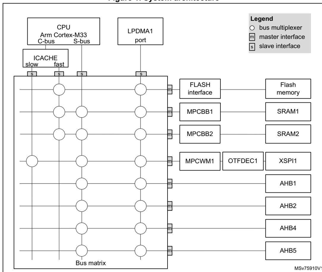
The diagram illustrates the system architecture of the microcontroller. At the top, the CPU (Arm Cortex-M33) is shown with its C-bus and S-bus. The C-bus connects to the ICACHE (slow and fast) and the Bus matrix. The S-bus connects to the Bus matrix. The LPDMA1 port connects to the Bus matrix. The Bus matrix is a central component that connects to various interfaces and peripherals. The interfaces include FLASH interface, MPCBB1, MPCBB2, MPCWM1, OTFDEC1, and XSPI1. The peripherals include Flash memory, SRAM1, SRAM2, AHB1, AHB2, AHB4, and AHB5. A legend indicates that a circle represents a bus multiplexer, a square with 'm' represents a master interface, and a square with 's' represents a slave interface. The diagram is labeled MSv75910V1.
2.1.1 CPU C-bus
This bus connects the C-bus of the CPU to the internal flash memory and to the bus matrix. This bus is used for instruction fetching and data access to the internal memories mapped in the code region. This bus targets the internal flash memory, internal SRAM (SRAM1 and SRAM2), and XSPI1 bank through the ICACHE address remap function.
2.1.2 CPU S-bus
This bus connects the system bus of the CPU to the bus matrix, and it is used by the core to access data located in a peripheral or SRAM area. This bus targets the internal SRAM (SRAM1 and SRAM2), XSPI1 bank, AHB1 peripherals including the APB1 and APB2 peripherals, AHB2, AHB4 peripherals including the APB7, and AHB5 peripherals.
2.1.3 LPDMA1-bus
The bus connects the AHB master interface of the LPDMA1 to the bus matrix. This targets the internal flash memory, the internal SRAM (SRAM1 and SRAM2), XSPI1 bank, AHB1 peripherals including the APB1 and APB2 peripherals, AHB2 peripherals, AHB4 peripherals including the APB7, and AHB5 peripherals.
2.1.4 Bus matrix
The bus matrix manages the access arbitration (based on fixed priority) between masters, and features a bus multiplexer used to connect each master to a given slave with no latency.
Table 1. Bus matrix access arbitration
| Master | Priority |
|---|---|
| Cpu core S-bus | 1 - highest |
| ICACHE slow port | 2 |
| ICACHE fast port | 3 |
| LPDMA1 | 4 - lowest |
2.1.5 AHB/APB bridges
The three bridges, AHB1 to APB1, AHB1 to APB2, and AHB4 to APB7, provide full synchronous connections between the AHB and the APB buses, resulting in the flexible selection of the peripheral frequency.
Refer to Section 2.3.2: Memory map and register boundary addresses for the address mapping of the peripherals connected to these bridges.
After each device reset, the clock of peripherals having a xxEN bit in the RCC is disabled. Before using a peripheral, its clock must be enabled in the RCC_AHBxENR and RCC_APBxENR registers.
Note: When a 16- or 8-bit access operation is performed on an APB register, it is transformed into a 32-bit access operation: the bridge duplicates the 16- or 8-bit data to feed the 32-bit vector.
The 2.4 GHz RADIO peripheral AHB5 is a semisynchronous bus, connected through a bridge to the bus matrix.
2.2 TrustZone ® security architecture
The security architecture is based on Arm ® TrustZone ® with the Armv8_M mainline extension.
The TZEN option bit in the FLASH_OPTR register activates TrustZone ® security.
When TrustZone ® is enabled, the SAU (security attribution unit) and IDAU (implementation-defined attribution unit) define the access permissions based on secure and nonsecure states.
- • SAU: up to eight SAU configurable regions are available for security attribution.
- • IDAU: provides a first memory partition as nonsecure or nonsecure callable attributes. The IDAU memory map partition is not configurable and fixed by hardware implementation (refer to Figure 2: Memory map ). It is then combined with the results from the SAU security attribution, and the highest security state is selected.
Based on IDAU security attribution, the flash memory, system SRAMs, and peripheral memory space are aliased twice for secure and nonsecure states. However, the external memory space is not aliased.
Table 2 shows a typical example of eight SAU regions mapping, based on IDAU regions. The user can split and choose the secure, nonsecure, or NSC regions for external memories according to application requirements.
Table 2. Memory map security attribution example vs. SAU configuration regions (1)
| Region description | Address range | IDAU security attribution | SAU security attribution typical configuration | Final security attribution |
|---|---|---|---|---|
| Reserved | 0x0000 0000 to 0x07FF FFFF | Nonsecure | Secure, nonsecure, or NSC | |
| Code Flash and SRAM | 0x0800 0000 to 0x0BFF FFFF | Nonsecure | Nonsecure | |
| 0x0C00 0000 to 0x0FFF FFFF | NSC | Secure or NSC | ||
| Reserved | 0x1000 0000 to 0x17FF FFFF | Nonsecure | ||
| 0x1800 0000 to 0x1FFF FFFF | ||||
| SRAM | 0x2000 0000 to 0x2FFF FFFF | Nonsecure | ||
| 0x3000 0000 to 0x3FFF FFFF | NSC | Secure or NSC | ||
| Peripherals | 0x4000 0000 to 0x4FFF FFFF | Nonsecure | Nonsecure | |
| 0x5000 0000 to 0x5FFF FFFF | NSC | Secure or NSC | ||
| External memories | 0x6000 0000 to 0xDFFF FFFF | Nonsecure | Secure, nonsecure, or NSC | |
1. NSC = nonsecure callable
2.2.1 Default TrustZone ® security state
When the TrustZone ® security is activated by the TZEN option bit in the FLASH_OPTR register, the default system security state is as detailed below:
- • CPU:
- – Core is in a secure state after reset. The boot address must point to a secure area.
- • Memory map:
- – SAU is fully secure after reset. Consequently, the entire memory map is fully secure. Up to eight SAU configurable regions are available for security attribution.
- • Flash memory:
- – The flash memory security area is defined by watermark user options.
- – Flash memory block-based security attributions are nonsecure after reset.
- • SRAMs:
- – SRAM1 and SRAM2 are secure after reset. MPCBBx (block-based memory protection controller) is secure.
- • External memories:
- – The XSPI bank is secure after reset. MPCWM (watermark-based memory protection controller) is secure.
- • Peripherals (see
Table 3
and
Table 4
for a list of securable and TrustZone
®
-aware peripherals):
- – Securable peripherals are nonsecure after reset.
- – TrustZone ® -aware peripherals are nonsecure after reset. Their secure configuration registers are secure.
- • All GPIOs are secure after reset.
- • Interrupts:
- – NVIC: all interrupts are secure after reset. NVIC is banked for secure and nonsecure states.
- – TZIC: all illegal access interrupts are disabled after reset (see Section 5.5: GTZC interrupts ).
2.2.2 TrustZone ® peripheral classification
When the TrustZone ® security is active, a peripheral can be either the securable or TrustZone ® -aware type as follows:
- • Securable: peripheral protected by an AHB/APB firewall gate controlled by the TZSC controller to define security properties
- • TrustZone ® -aware: peripheral connected directly to the AHB or APB bus and implementing specific TrustZone ® behavior, such as a subset of registers being secure.
Refer to Section 5: Global TrustZone ® controller (GTZC) for more details.
Table 3 and Table 4 list the securable and TrustZone ® -aware peripherals within the system.
Table 3. Securable peripherals by TZSC
| Bus | Peripheral |
|---|---|
| AHB5 | 2.4 GHz RADIO + SEQRAM |
| PTACONV |
| Bus | Peripheral |
|---|---|
| AHB4 | ADC4 |
| AHB2 | XSPI1 and DLYBXS1 (1) |
| PKA | |
| RNG | |
| HASH | |
| AES | |
| AHB1 | ICACHE registers |
| CRC | |
| RAMCFG | |
| APB7 | LPTIM1 |
| I2C3 | |
| LPUART1 | |
| SPI3 | |
| APB2 | TIM17 |
| TIM16 | |
| USB (1) | |
| SAI1 | |
| USART1 | |
| APB1 | LPTIM2 |
| I2C1 | |
| IWDG | |
| TIM2 |
1. Only available on STM32WBA25xx devices.
Table 4. TrustZone ® -aware peripherals| Bus | Peripheral |
|---|---|
| AHB4 | EXTI |
| RCC | |
| PWR | |
| AHB2 | OTFDEC1 (1) |
| GPIOH | |
| GPIOC | |
| GPIOB | |
| GPIOA |
| Bus | Peripheral |
|---|---|
| AHB1 | GTZC1-MPCBB2 |
| GTZC1-MPCBB1 | |
| GTZC1-TZSC | |
| GTZC1-TZIC | |
| FLASH interface | |
| LPDMA1 | |
| APB7 | TAMP |
| RTC | |
| SYSCFG |
1. Only available on STM32WBA25xx devices.
2.3 Memory organization
2.3.1 Introduction
Program memory, data memory, registers and I/O ports are organized within the same linear address space.
The bytes are coded in memory in Little Endian format. The lowest numbered byte in a word is considered the word's least significant byte and the highest numbered byte the most significant.
The addressable memory space is divided into eight main blocks, of 512 Mbytes each.
2.3.2 Memory map and register boundary addresses
Figure 2. Memory map
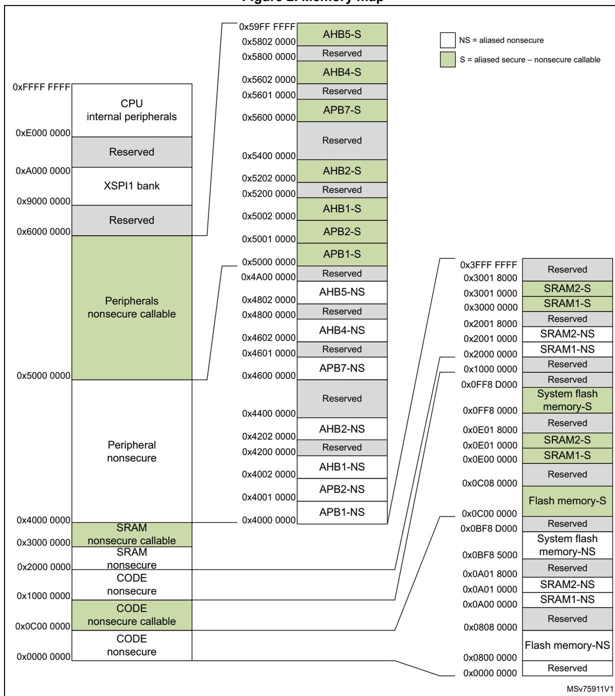
Legend:
- □ NS = aliased nonsecure
- ■ S = aliased secure – nonsecure callable
Memory Map:
| Address Range | Memory Region | Security Status |
|---|---|---|
| 0x0000 0000 – 0x00800 0000 | CODE nonsecure | NS |
| 0x00800 0000 – 0x00A00 0000 | Reserved | NS |
| 0x00A00 0000 – 0x01000 0000 | CODE nonsecure callable | S |
| 0x01000 0000 – 0x02000 0000 | CODE nonsecure | NS |
| 0x02000 0000 – 0x04000 0000 | SRAM nonsecure | NS |
| 0x04000 0000 – 0x05000 0000 | SRAM nonsecure callable | S |
| 0x05000 0000 – 0x06000 0000 | Peripheral nonsecure | NS |
| 0x06000 0000 – 0x09000 0000 | Reserved | NS |
| 0x09000 0000 – 0x0A000 0000 | XSPI1 bank | NS |
| 0x0A000 0000 – 0x0E000 0000 | Reserved | NS |
| 0x0E000 0000 – 0xFFFF FFFF | CPU internal peripherals | NS |
Peripheral and SRAM Details:
| Address Range | Memory Region | Security Status |
|---|---|---|
| 0x4000 0000 – 0x4002 0000 | APB1-NS | NS |
| 0x4002 0000 – 0x4004 0000 | APB2-NS | NS |
| 0x4004 0000 – 0x4006 0000 | APB3-NS | NS |
| 0x4006 0000 – 0x4008 0000 | APB4-NS | NS |
| 0x4008 0000 – 0x4010 0000 | APB5-NS | NS |
| 0x4010 0000 – 0x4012 0000 | Reserved | NS |
| 0x4012 0000 – 0x4014 0000 | APB1-S | S |
| 0x4014 0000 – 0x4016 0000 | APB2-S | S |
| 0x4016 0000 – 0x4018 0000 | APB3-S | S |
| 0x4018 0000 – 0x4020 0000 | APB4-S | S |
| 0x4020 0000 – 0x4022 0000 | APB5-S | S |
| 0x4022 0000 – 0x4024 0000 | Reserved | NS |
| 0x4024 0000 – 0x4026 0000 | APB1-S | S |
| 0x4026 0000 – 0x4028 0000 | APB2-S | S |
| 0x4028 0000 – 0x4030 0000 | APB3-S | S |
| 0x4030 0000 – 0x4032 0000 | APB4-S | S |
| 0x4032 0000 – 0x4034 0000 | APB5-S | S |
| 0x4034 0000 – 0x4036 0000 | Reserved | NS |
| 0x4036 0000 – 0x4038 0000 | APB1-S | S |
| 0x4038 0000 – 0x4040 0000 | APB2-S | S |
| 0x4040 0000 – 0x4042 0000 | APB3-S | S |
| 0x4042 0000 – 0x4044 0000 | APB4-S | S |
| 0x4044 0000 – 0x4046 0000 | APB5-S | S |
| 0x4046 0000 – 0x4048 0000 | Reserved | NS |
| 0x4048 0000 – 0x4050 0000 | APB1-S | S |
| 0x4050 0000 – 0x4052 0000 | APB2-S | S |
| 0x4052 0000 – 0x4054 0000 | APB3-S | S |
| 0x4054 0000 – 0x4056 0000 | APB4-S | S |
| 0x4056 0000 – 0x4058 0000 | APB5-S | S |
| 0x4058 0000 – 0x4060 0000 | Reserved | NS |
| 0x4060 0000 – 0x4062 0000 | APB1-S | S |
| 0x4062 0000 – 0x4064 0000 | APB2-S | S |
| 0x4064 0000 – 0x4066 0000 | APB3-S | S |
| 0x4066 0000 – 0x4068 0000 | APB4-S | S |
| 0x4068 0000 – 0x4070 0000 | APB5-S | S |
| 0x4070 0000 – 0x4072 0000 | Reserved | NS |
| 0x4072 0000 – 0x4074 0000 | APB1-S | S |
| 0x4074 0000 – 0x4076 0000 | APB2-S | S |
| 0x4076 0000 – 0x4078 0000 | APB3-S | S |
| 0x4078 0000 – 0x4080 0000 | APB4-S | S |
| 0x4080 0000 – 0x4082 0000 | APB5-S | S |
| 0x4082 0000 – 0x4084 0000 | Reserved | NS |
| 0x4084 0000 – 0x4086 0000 | APB1-S | S |
| 0x4086 0000 – 0x4088 0000 | APB2-S | S |
| 0x4088 0000 – 0x4090 0000 | APB3-S | S |
| 0x4090 0000 – 0x4092 0000 | APB4-S | S |
| 0x4092 0000 – 0x4094 0000 | APB5-S | S |
| 0x4094 0000 – 0x4096 0000 | Reserved | NS |
| 0x4096 0000 – 0x4098 0000 | APB1-S | S |
| 0x4098 0000 – 0x409A 0000 | APB2-S | S |
| 0x409A 0000 – 0x409C 0000 | APB3-S | S |
| 0x409C 0000 – 0x409E 0000 | APB4-S | S |
| 0x409E 0000 – 0x40A0 0000 | APB5-S | S |
| 0x40A0 0000 – 0x40A2 0000 | Reserved | NS |
| 0x40A2 0000 – 0x40A4 0000 | APB1-S | S |
| 0x40A4 0000 – 0x40A6 0000 | APB2-S | S |
| 0x40A6 0000 – 0x40A8 0000 | APB3-S | S |
| 0x40A8 0000 – 0x40AA 0000 | APB4-S | S |
| 0x40AA 0000 – 0x40AC 0000 | APB5-S | S |
| 0x40AC 0000 – 0x40AE 0000 | Reserved | NS |
| 0x40AE 0000 – 0x40B0 0000 | APB1-S | S |
| 0x40B0 0000 – 0x40B2 0000 | APB2-S | S |
| 0x40B2 0000 – 0x40B4 0000 | APB3-S | S |
| 0x40B4 0000 – 0x40B6 0000 | APB4-S | S |
| 0x40B6 0000 – 0x40B8 0000 | APB5-S | S |
| 0x40B8 0000 – 0x40BA 0000 | Reserved | NS |
| 0x40BA 0000 – 0x40BC 0000 | APB1-S | S |
| 0x40BC 0000 – 0x40BE 0000 | APB2-S | S |
| 0x40BE 0000 – 0x40C0 0000 | APB3-S | S |
| 0x40C0 0000 – 0x40C2 0000 | APB4-S | S |
| 0x40C2 0000 – 0x40C4 0000 | APB5-S | S |
| 0x40C4 0000 – 0x40C6 0000 | Reserved | NS |
| 0x40C6 0000 – 0x40C8 0000 | APB1-S | S |
| 0x40C8 0000 – 0x40CA 0000 | APB2-S | S |
| 0x40CA 0000 – 0x40CC 0000 | APB3-S | S |
| 0x40CC 0000 – 0x40CE 0000 | APB4-S | S |
| 0x40CE 0000 – 0x40D0 0000 | APB5-S | S |
| 0x40D0 0000 – 0x40D2 0000 | Reserved | NS |
| 0x40D2 0000 – 0x40D4 0000 | APB1-S | S |
| 0x40D4 0000 – 0x40D6 0000 | APB2-S | S |
| 0x40D6 0000 – 0x40D8 0000 | APB3-S | S |
| 0x40D8 0000 – 0x40DA 0000 | APB4-S | S |
| 0x40DA 0000 – 0x40DC 0000 | APB5-S | S |
| 0x40DC 0000 – 0x40DE 0000 | Reserved | NS |
| 0x40DE 0000 – 0x40E0 0000 | APB1-S | S |
| 0x40E0 0000 – 0x40E2 0000 | APB2-S | S |
| 0x40E2 0000 – 0x40E4 0000 | APB3-S | S |
| 0x40E4 0000 – 0x40E6 0000 | APB4-S | S |
| 0x40E6 0000 – 0x40E8 0000 | APB5-S | S |
| 0x40E8 0000 – 0x40EA 0000 | Reserved | NS |
| 0x40EA 0000 – 0x40EC 0000 | APB1-S | S |
| 0x40EC 0000 – 0x40EE 0000 | APB2-S | S |
| 0x40EE 0000 – 0x40F0 0000 | APB3-S | S |
| 0x40F0 0000 – 0x40F2 0000 | APB4-S | S |
| 0x40F2 0000 – 0x40F4 0000 | APB5-S | S |
| 0x40F4 0000 – 0x40F6 0000 | Reserved | NS |
| 0x40F6 0000 – 0x40F8 0000 | APB1-S | S |
| 0x40F8 0000 – 0x40FA 0000 | APB2-S | S |
| 0x40FA 0000 – 0x40FC 0000 | APB3-S | S |
| 0x40FC 0000 – 0x40FE 0000 | APB4-S | S |
| 0x40FE 0000 – 0x4100 0000 | APB5-S | S |
| 0x4100 0000 – 0x4102 0000 | Reserved | NS |
| 0x4102 0000 – 0x4104 0000 | APB1-S | S |
| 0x4104 0000 – 0x4106 0000 | APB2-S | S |
| 0x4106 0000 – 0x4108 0000 | APB3-S | S |
| 0x4108 0000 – 0x410A 0000 | APB4-S | S |
| 0x410A 0000 – 0x410C 0000 | APB5-S | S |
| 0x410C 0000 – 0x410E 0000 | Reserved | NS |
| 0x410E 0000 – 0x4110 0000 | APB1-S | S |
| 0x4110 0000 – 0x4112 0000 | APB2-S | S |
| 0x4112 0000 – 0x4114 0000 | APB3-S | S |
| 0x4114 0000 – 0x4116 0000 | APB4-S | S |
| 0x4116 0000 – 0x4118 0000 | APB5-S | S |
| 0x4118 0000 – 0x411A 0000 | Reserved | NS |
| 0x411A 0000 – 0x411C 0000 | APB1-S | S |
| 0x411C 0000 – 0x411E 0000 | APB2-S | S |
| 0x411E 0000 – 0x4120 0000 | APB3-S | S |
| 0x4120 0000 – 0x4122 0000 | APB4-S | S |
| 0x4122 0000 – 0x4124 0000 | APB5-S | S |
| 0x4124 0000 – 0x4126 0000 | Reserved | NS |
| 0x4126 0000 – 0x4128 0000 | APB1-S | S |
| 0x4128 0000 – 0x412A 0000 | APB2-S | S |
| 0x412A 0000 – 0x412C 0000 | APB3-S | S |
| 0x412C 0000 – 0x412E 0000 | APB4-S | S |
| 0x412E 0000 – 0x4130 0000 | APB5-S | S |
| 0x4130 0000 – 0x4132 0000 | Reserved | NS |
| 0x4132 0000 – 0x4134 0000 | APB1-S | S |
| 0x4134 0000 – 0x4136 0000 | APB2-S | S |
| 0x4136 0000 – 0x4138 0000 | APB3-S | S |
| 0x4138 0000 – 0x413A 0000 | APB4-S | S |
| 0x413A 0000 – 0x413C 0000 | APB5-S | S |
| 0x413C 0000 – 0x413E 0000 | Reserved | NS |
| 0x413E 0000 – 0x4140 0000 | APB1-S | S |
| 0x4140 0000 – 0x4142 0000 | APB2-S | S |
| 0x4142 0000 – 0x4144 0000 | APB3-S | S |
| 0x4144 0000 – 0x4146 0000 | APB4-S | S |
| 0x4146 0000 – 0x4148 0000 | APB5-S | S |
| 0x4148 0000 – 0x414A 0000 | Reserved | NS |
| 0x414A 0000 – 0x414C 0000 | APB1-S | S |
| 0x414C 0000 – 0x414E 0000 | APB2-S | S |
| 0x414E 0000 – 0x4150 0000 | APB3-S | S |
| 0x4150 0000 – 0x4152 0000 | APB4-S | S |
| 0x4152 0000 – 0x4154 0000 | APB5-S | S |
| 0x4154 0000 – 0x4156 0000 | Reserved | NS |
| 0x4156 0000 – 0x4158 0000 | APB1-S | S |
| 0x4158 0000 – 0x415A 0000 | APB2-S | S |
| 0x415A 0000 – 0x415C 0000 | APB3-S | S |
| 0x415C 0000 – 0x415E 0000 | APB4-S | S |
| 0x415E 0000 – 0x4160 0000 | APB5-S | S |
| 0x4160 0000 – 0x4162 0000 | Reserved | NS |
| 0x4162 0000 – 0x4164 0000 | APB1-S | S |
| 0x4164 0000 – 0x4166 0000 | APB2-S | S |
| 0x4166 0000 – 0x4168 0000 | APB3-S | S |
| 0x4168 0000 – 0x416A 0000 | APB4-S | S |
| 0x416A 0000 – 0x416C 0000 | APB5-S | S |
| 0x416C 0000 – 0x416E 0000 | Reserved | NS |
| 0x416E 0000 – 0x4170 0000 | APB1-S | S |
| 0x4170 0000 – 0x4172 0000 | APB2-S | S |
| 0x4172 0000 – 0x4174 0000 | APB3-S | S |
| 0x4174 0000 – 0x4176 0000 | APB4-S | S |
| 0x4176 0000 – 0x4178 0000 | APB5-S | S |
| 0x4178 0000 – 0x417A 0000 | Reserved | NS |
| 0x417A 0000 – 0x417C 0000 | APB1-S | S |
| 0x417C 0000 – 0x417E 0000 | APB2-S | S |
| 0x417E 0000 – 0x4180 0000 | APB3-S | S |
| 0x4180 0000 – 0x4182 0000 | APB4-S | S |
| 0x4182 0000 – 0x4184 0000 | APB5-S | S |
| 0x4184 0000 – 0x4186 0000 | Reserved | NS |
| 0x4186 0000 – 0x4188 0000 | APB1-S | S |
| 0x4188 0000 – 0x418A 0000 | APB2-S | S |
| 0x418A 0000 – 0x418C 0000 | APB3-S | S |
| 0x418C 0000 – 0x418E 0000 | APB4-S | S |
| 0x418E 0000 – 0x4190 0000 | APB5-S | S |
| 0x4190 0000 – 0x4192 0000 | Reserved | NS |
| 0x4192 0000 – 0x4194 0000 | APB1-S | S |
| 0x4194 0000 – 0x4196 0000 | APB2-S | S |
| 0x4196 0000 – 0x4198 0000 | APB3-S | S |
| 0x4198 0000 – 0x419A 0000 | APB4-S | S |
| 0x419A 0000 – 0x419C 0000 | APB5-S | S |
| 0x419C 0000 – 0x419E 0000 | Reserved | NS |
| 0x419E 0000 – 0x41A0 0000 | APB1-S | S |
| 0x41A0 0000 – 0x41A2 0000 | APB2-S | S |
| 0x41A2 0000 – 0x41A4 0000 | APB3-S | S |
| 0x41A4 0000 – 0x41A6 0000 | APB4-S | S |
| 0x41A6 0000 – 0x41A8 0000 | APB5-S | S |
| 0x41A8 0000 – 0x41AA 0000 | Reserved | NS |
| 0x41AA 0000 – 0x41AC 0000 | APB1-S | S |
| 0x41AC 0000 – 0x41AE 0000 | APB2-S | S |
| 0x41AE 0000 – 0x41B0 0000 | APB3-S | S |
| 0x41B0 0000 – 0x41B2 0000 | APB4-S | S |
| 0x41B2 0000 – 0x41B4 0000 | APB5-S | S |
| 0x41B4 0000 – 0x41B6 0000 | Reserved | NS |
| 0x41B6 0000 – 0x41B8 0000 | APB1-S | S |
| 0x41B8 0000 – 0x41BA 0000 | APB2-S | S |
| 0x41BA 0000 – 0x41BC 0000 | APB3-S | S |
| 0x41BC 0000 – 0x41BE 0000 | APB4-S | S |
| 0x41BE 0000 – 0x41C0 0000 | APB5-S | S |
| 0x41C0 0000 – 0x41C2 0000 | Reserved | NS |
| 0x41C2 0000 – 0x41C4 0000 | APB1-S | S |
| 0x41C4 0000 – 0x41C6 0000 | APB2-S | S |
| 0x41C6 0000 – 0x41C8 0000 | APB3-S | S |
| 0x41C8 0000 – 0x41CA 0000 | APB4-S | S |
| 0x41CA 0000 – 0x41CC 0000 | APB5-S | S |
| 0x41CC 0000 – 0x41CE 0000 | Reserved | NS |
| 0x41CE 0000 – 0x41D0 0000 | APB1-S | S |
| 0x41D0 0000 – 0x41D2 0000 | APB2-S | S |
| 0x41D2 0000 – 0x41D4 0000 | APB3-S | S |
| 0x41D4 0000 – 0x41D6 0000 | APB4-S | S |
| 0x41D6 0000 – 0x41D8 0000 | APB5-S | S |
| 0x41D8 0000 – 0x41DA 0000 | Reserved | NS |
| 0x41DA 0000 – 0x41DC 0000 | APB1-S | S |
| 0x41DC 0000 – 0x41DE 0000 | APB2-S | S |
| 0x41DE 0000 – 0x41E0 0000 | APB3-S | S |
| 0x41E0 0000 – 0x41E2 0000 | APB4-S | S |
| 0x41E2 0000 – 0x41E4 0000 | APB5-S | S |
| 0x41E4 0000 – 0x41E6 0000 | Reserved | NS |
| 0x41E6 0000 – 0x41E8 0000 |
Table 5 gives the boundary addresses of the peripherals available in the device.
!!! LINKS TO BE UPDATED !!!
Table 5. Memory map and peripheral register boundary addresses
| Bus | Secure Boundary address (1) | Nonsecure Boundary address (1) | Size (bytes) | Peripheral | Peripheral register map |
|---|---|---|---|---|---|
| - | 0xA000 0000 - 0xDFFF FFFF | 0xA000 0000 - 0xDFFF FFFF | - | Reserved | - |
| - | 0x9000 0000 - 0x9FFF FFFF | 0x9000 0000 - 0x9FFF FFFF | 256 M | XSPI1 bank (2) | - |
| - | 0x5A00 0000 - 0x8FFF FFFF | 0x4A00 0000 - 0x8FFF FFFF | - | Reserved | - |
| AHB5 | 0x5803 8400 - 0x59FF FFFF | 0x4803 8400 - 0x49FF FFFF | - | Reserved | - |
| 0x5803 8000 - 0x5803 83FF | 0x4803 8000 - 0x4803 83FF | 1 K | PTACONV | Section 10.5.4 on page 281 | |
| 0x5802 A800 - 0x5803 7FFF | 0x4802 A800 - 0x4803 7FFF | - | Reserved | - | |
| 0x5802 8000 - 0x5802 A7FF | 0x4802 8000 - 0x4802 A7FF | 10 K | RXTXRAM | - | |
| 0x5802 1200 - 0x5802 7FFF | 0x4802 1200 - 0x4802 7FFF | - | Reserved | - | |
| 0x5802 1000 - 0x5802 11FF | 0x4802 1000 - 0x4802 11FF | 0.5 K | SEQRAM | - | |
| 0x5802 0000 - 0x5802 0FFF | 0x4802 0000 - 0x4802 0FFF | 4 K | 2.4 GHz RADIO | - | |
| - | 0x5800 0000 - 0x5801 FFFF | 0x4800 0000 - 0x4801 FFFF | - | Reserved | - |
| AHB4 | 0x5602 2400 - 0x57FF FFFF | 0x4602 2400 - 0x47FF FFFF | - | Reserved | - |
| 0x5602 2000 - 0x5602 23FF | 0x4602 2000 - 0x4602 23FF | 1 K | EXTI | Section 18.6.15 on page 609 | |
| 0x5602 1400 - 0x5602 1FFF | 0x4602 1400 - 0x4602 1FFF | - | Reserved | - | |
| 0x5602 1000 - 0x5602 13FF | 0x4602 1000 - 0x4602 13FF | 1 K | ADC4 | Section 22.7.18 on page 719 | |
| 0x5602 0C00 - 0x5602 0FFF | 0x4602 0C00 - 0x4602 0FFF | 1 K | RCC | Section 12.8.54 on page 449 | |
| 0x5602 0800 - 0x5602 0BFF | 0x4602 0800 - 0x4602 0BFF | 1 K | PWR | Section 11.10.25 on page 346 | |
| 0x5602 0000 - 0x5602 07FF | 0x4602 0000 - 0x4602 07FF | - | Reserved | - | |
| - | 0x5601 0000 - 0x5601 FFFF | 0x4601 0000 - 0x4601 FFFF | - | Reserved | - |
Table 5. Memory map and peripheral register boundary addresses (continued)
| Bus | Secure Boundary address (1) | Nonsecure Boundary address (1) | Size (bytes) | Peripheral | Peripheral register map |
|---|---|---|---|---|---|
| APB7 | 0x5600 8000 - 0x5600 FFFF | 0x4600 8000 - 0x4600 FFFF | - | Reserved | - |
| 0x5600 7C00 - 0x5600 7FFF | 0x4600 7C00 - 0x4600 7FFF | 1 K | TAMP | Section 34.6.19 on page 1198 | |
| 0x5600 7800 - 0x5600 7BFF | 0x4600 7800 - 0x4600 7BFF | 1 K | RTC | Section 33.6.26 on page 1154 | |
| 0x5600 4800 - 0x5600 77FF | 0x4600 4800 - 0x4600 77FF | - | Reserved | - | |
| 0x5600 4400 - 0x5600 47FF | 0x4600 4400 - 0x4600 47FF | 1 K | LPTIM1 | Section 30.7.16 on page 1084 | |
| 0x5600 2C00 - 0x5600 43FF | 0x4600 2C00 - 0x4600 43FF | - | Reserved | - | |
| 0x5600 2800 - 0x5600 2BFF | 0x4600 2800 - 0x4600 2BFF | 1 K | I2C3 | Section 35.9.13 on page 1266 | |
| 0x5600 2400 - 0x5600 27FF | 0x4600 2400 - 0x4600 27FF | 1 K | LPUART1 | Section 37.7.15 on page 1410 | |
| 0x5600 2000 - 0x5600 23FF | 0x4600 2000 - 0x4600 23FF | 1 K | SPI3 | Section 38.8.15 on page 1462 | |
| 0x5600 0800 - 0x5600 1FFF | 0x4600 0800 - 0x4600 1FFF | - | Reserved | ||
| 0x5600 0400 - 0x5600 07FF | 0x4600 0400 - 0x4600 07FF | 1 K | SYSCFG | Section 14.3.11 on page 516 | |
| 0x5600 0000 - 0x5600 03FF | 0x4600 0000 - 0x4600 03FF | - | Reserved | - | |
| - | 0x5400 0000 - 0x55FF FFFF | 0x4400 0000 - 0x45FF FFFF | - | Reserved | - |
Table 5. Memory map and peripheral register boundary addresses (continued)
| Bus | Secure Boundary address (1) | Nonsecure Boundary address (1) | Size (bytes) | Peripheral | Peripheral register map |
|---|---|---|---|---|---|
| AHB2 | 0x520D 1800 - 0x53FF FFFF | 0x420D 1800 - 0x43FF FFFF | - | Reserved | - |
| 0x520D 1400 - 0x520D 17FF | 0x420D 1400 - 0x420D 17FF | 1 K | XSPI1 (2) | Section 20.7.14 on page 651 | |
| 0x520C F400 - 0x520D 13FF | 0x420C F400 - 0x420D 13FF | - | Reserved | - | |
| 0x520C F000 - 0x520C F3FF | 0x420C F000 - 0x420C F3FF | 1 K | DLYBXS1 (2) | Section 21.5.3 on page 658 | |
| 0x520C 5400 - 0x520C EFFF | 0x420C 5400 - 0x420C EFFF | - | Reserved | - | |
| 0x520C 5000 - 0x520C 53FF | 0x420C 5000 - 0x420C 53FF | 1 K | OTFDEC1 (2) | Section 26.6.15 on page 825 | |
| 0x520C 4000 - 0x530C 4FFF | 0x420C 4000 - 0x420C 4FFF | - | Reserved | - | |
| 0x520C 3C00 - 0x520C 3FFF | 0x420C 3C00 - 0x420C 3FFF | 8 K | PKA continue | Section 27.8.5 on page 861 | |
| 0x520C 2400 - 0x520C 3BFF | 0x420C 2400 - 0x420C 3BFF | PKA RAM | |||
| 0x520C 2000 - 0x520C 23FF | 0x420C 2000 - 0x420C 23FF | PKA | |||
| 0x520C 0C00 - 0x520C 1FFF | 0x420C 0C00 - 0x420C 1FFF | - | Reserved | - | |
| 0x520C 0800 - 0x520C 0BFF | 0x420C 0800 - 0x420C 0BFF | 1 K | RNG | Section 23.7.9 on page 741 | |
| 0x520C 0400 - 0x520C 07FF | 0x420C 0400 - 0x420C 07FF | 1 K | HASH | Section 25.6.8 on page 804 | |
| 0x520C 0000 - 0x520C 03FF | 0x420C 0000 - 0x420C 03FF | 1 K | AES | Section 24.9.21 on page 783 | |
| 0x5202 2000 - 0x520B FFFF | 0x4202 2000 - 0x420B FFFF | - | Reserved | - | |
| 0x5202 1C00 - 0x5202 1FFF | 0x4202 1C00 - 0x4202 1FFF | 1 K | GPIOH | Section 13.8.1 on page 493 | |
| 0x5202 0C00 - 0x5202 1BFF | 0x4202 0C00 - 0x4202 1BFF | - | Reserved | - | |
| 0x5202 0800 - 0x5202 0BFF | 0x4202 0800 - 0x4202 0BFF | 1 K | GPIOC | Section 13.7.1 on page 487 | |
| 0x5202 0400 - 0x5202 07FF | 0x4202 0400 - 0x4202 07FF | 1 K | GPIOB | Section 13.6.1 on page 477 | |
| 0x5202 0000 - 0x5202 03FF | 0x4202 0000 - 0x4202 03FF | 1 K | GPIOA | Section 13.5.1 on page 469 | |
| - | 0x5200 0000 - 0x5201 FFFF | 0x4200 0000 - 0x4201 FFFF | - | Reserved | - |
| AHB1 | 0x5002 3400 - 0x51FF FFFF | 0x4002 3400 - 0x41FF FFFF | - | Reserved | - |
| 0x5003 3000 - 0x5003 33FF | 0x4003 3000 - 0x4003 33FF | 1 K | GTZC1_MPCBB2 | Section 5.8 on page 158 | |
| 0x5003 2C00 - 0x5003 2FFF | 0x4003 2C00 - 0x4003 2FFF | 1 K | GTZC1_MPCBB1 | Section 5.8 on page 158 | |
| 0x5003 2800 - 0x5003 2BFF | 0x4003 2800 - 0x4003 2BFF | 1 K | GTZC1_TZIC | Section 5.7 on page 142 | |
| 0x5003 2400 - 0x5003 27FF | 0x4003 2400 - 0x4003 27FF | 1 K | GTZC1_TZSC | Section 5.6 on page 128 | |
| 0x5003 0800 - 0x5003 23FF | 0x4003 0800 - 0x5003 23FF | - | Reserved | - | |
| 0x5003 0400 - 0x5003 07FF | 0x4003 0400 - 0x4003 07FF | 1 K | ICACHE | Section 8.7.8 on page 264 | |
| 0x5002 7000 - 0x5003 03FF | 0x4002 7000 - 0x4003 03FF | - | Reserved | - | |
| 0x5002 6000 - 0x5002 6FFF | 0x4002 6000 - 0x4002 6FFF | 4 K | RAMCFG | Section 6.6.4 on page 170 | |
| 0x5002 3400 - 0x5002 5FFF | 0x4002 3400 - 0x4002 5FFF | - | Reserved | - | |
| 0x5002 3000 - 0x5002 33FF | 0x4002 3000 - 0x4002 33FF | 1 K | CRC | Section 19.4.6 on page 617 | |
| 0x5002 2400 - 0x5002 2FFF | 0x4002 2400 - 0x4002 2FFF | - | Reserved | - | |
| 0x5002 2000 - 0x5002 23FF | 0x4002 2000 - 0x4002 23FF | 1 K | FLASH interface | Section 7.9.36 on page 245 | |
| 0x5002 1000 - 0x5002 1FFF | 0x4002 1000 - 0x4002 1FFF | - | Reserved | - | |
| 0x5002 0000 - 0x5002 0FFF | 0x4002 0000 - 0x4002 0FFF | 4 K | LPDMA1 | Section 16.8.16 on page 584 |
Table 5. Memory map and peripheral register boundary addresses (continued)
| Bus | Secure Boundary address (1) | Nonsecure Boundary address (1) | Size (bytes) | Peripheral | Peripheral register map |
|---|---|---|---|---|---|
| APB2 | 0x5001 6C00 - 0x5001 FFFF | 0x4001 6C00 - 0x4001 FFFF | - | Reserved | - |
| 0x5001 6400 - 0x5001 6BFF | 0x4001 6400 - 0x4001 6BFF | 2 K | USB SRAM (2) | Section 40.6.8 on page 1568 | |
| 0x5001 6000 - 0x5001 63FF | 0x4001 6000 - 0x4001 63FF | 1 K | USB (2) | Section 40.6.8 on page 1568 | |
| 0x5001 5800 - 0x5001 5FFF | 0x4001 5800 - 0x4001 5FFF | - | Reserved | - | |
| 0x5001 5400 - 0x5001 57FF | 0x4001 5400 - 0x4001 57FF | 1 K | SAI1 | Section 39.6.19 on page 1526 | |
| 0x5001 4C00 - 0x5001 53FF | 0x4001 4C00 - 0x4001 53FF | - | Reserved | - | |
| 0x5001 4800 - 0x5001 4BFF | 0x4001 4800 - 0x4001 4BFF | 1 K | TIM17 | Section 29.7.22 on page 1038 | |
| 0x5001 4400 - 0x5001 47FF | 0x4001 4400 - 0x4001 47FF | 1 K | TIM16 | Section 29.7.22 on page 1038 | |
| 0x5001 3C00 - 0x5001 43FF | 0x4001 3C00 - 0x4001 43FF | - | Reserved | - | |
| 0x5001 3800 - 0x5001 3BFF | 0x4001 3800 - 0x4001 3BFF | 1 K | USART1 | Section 36.8.17 on page 1355 | |
| APB1 | 0x5001 0000 - 0x5001 37FF | 0x4001 0000 - 0x4001 37FF | - | Reserved | - |
| 0x5000 9800 - 0x5000 FFFF | 0x4000 9800 - 0x4000 FFFF | - | Reserved | - | |
| 0x5000 9400 - 0x5000 97FF | 0x4000 9400 - 0x4000 97FF | 1 K | LPTIM2 | Section 30.7.16 on page 1084 | |
| 0x5000 5800 - 0x5000 93FF | 0x4000 5800 - 0x4000 93FF | - | Reserved | - | |
| 0x5000 5400 - 0x5000 57FF | 0x4000 5400 - 0x4000 57FF | 1 K | I2C1 | Section 35.9.13 on page 1266 | |
| 0x5000 3400 - 0x5000 53FF | 0x4000 3400 - 0x4000 53FF | - | Reserved | - | |
| 0x5000 3000 - 0x5000 33FF | 0x4000 3000 - 0x4000 33FF | 1 K | IWDG | Section 32.7.7 on page 1101 | |
| 0x5000 0400 - 0x5000 2FFF | 0x4000 0400 - 0x4000 2FFF | - | Reserved | - | |
| 0x5000 0000 - 0x5000 03FF | 0x4000 0000 - 0x4000 03FF | 1 K | TIM2 | Section 28.5.25 on page 972 |
Table 5. Memory map and peripheral register boundary addresses (continued)
| Bus | Secure Boundary address (1) | Nonsecure Boundary address (1) | Size (bytes) | Peripheral | Peripheral register map |
|---|---|---|---|---|---|
| AHB | 0x3802 A800 - 0x4FFF FFFF | 0x2802 A800 - 0x3FFF FFFF | - | Reserved | - |
| 0x3802 8000 - 0x3802 A7FF | 0x2802 8000 - 0x2802 A7FF | 10 K | RXTXSRAM | ||
| 0x3001 8000 - 0x3802 7FFF | 0x2001 8000 - 0x2802 7FFF | - | Reserved | - | |
| 0x3001 2000 - 0x3001 7FFF | 0x2001 2000 - 0x2001 7FFF | 24 K | SRAM2 page 2 | ||
| 0x3001 0000 - 0x3001 1FFF | 0x2001 0000 - 0x2001 1FFF | 8 K | SRAM2 page 1 | ||
| 0x3000 0000 - 0x3000 FFFF | 0x2000 0000 - 0x2000 FFFF | 64 K | SRAM1 | - | |
| 0x0FF9 0000 - 0x2FFF FFFF | 0x0BF9 0000 - 0x1FFF FFFF | - | Reserved | - | |
| 0x0FF8 E000 - 0x0FF8 FFFF | 0x0BF8 E000 - 0x0BF8 FFFF | 16 K | Flash memory user options | Section 7.4.1 on page 191 | |
| 0x0FF8 D500 - 0x0FF8 DFFF | 0x0BF8 D500 - 0x0BF8 DFFF | 2.75 K | DESIG | Section 42.1.11 on page 1724 | |
| 0x0FF8 D200 - 0x0FF8 D4FF | 0x0BF8 D200 - 0x0BF8 D4FF | - | Reserved | - | |
| 0x0FF8 D000 - 0x0FF8 D1FF | 0x0BF8 D000 - 0x0BF8 D1FF | 512 | OTP | - | |
| 0x0FF8 5000 - 0x0FF8 CFFF | 0x0BF8 5000 - 0x0BF8 CFFF | 32 K | Bootloader | - | |
| 0x0FF8 4000 - 0x0FF8 4FFF | 0x0BF8 4000 - 0x0BF8 4FFF | 4 K | RSS-Lib | - | |
| 0x0FF8 0000 - 0x0FF8 3FFF | 0x0BF8 0000 - 0x0BF8 3FFF | 16 K | RSS-Boot | - | |
| 0x0E01 8000 - 0x0FF7 FFFF | 0x0A01 8000 - 0x0BF7 FFFF | - | Reserved | - | |
| 0x0E01 2000 - 0x0E01 7FFF | 0x0A01 2000 - 0x0A01 7FFF | 24 K | SRAM2 page 2 | ||
| 0x0E01 0000 - 0x0E01 1FFF | 0x0A01 0000 - 0x0A01 1FFF | 8 K | SRAM2 page 1 | ||
| 0x0E00 0000 - 0x0E00 FFFF | 0x0A00 0000 - 0x0A00 FFFF | 64 K | SRAM1 | - | |
| 0x0C08 0000 - 0x0DFF FFFF | 0x0808 0000 - 0x09FF FFFF | - | Reserved | - | |
| 0x0C00 0000 - 0x0C07 FFFF | 0x0800 0000 - 0x0807 FFFF | 512 K | User flash memory | - | |
| 0x0000 0000 - 0x0BFF FFFF | 0x0000 0000 - 0x07FF FFFF | - | Reserved | - |
1. Gray shaded fields are reserved.
2. Only available on STM32WBA25xx devices.
2.3.3 Embedded SRAM
The devices feature 96-Kbyte SRAMs:
- • SRAM1: 64 Kbytes
- • SRAM2: 32 Kbytes in two pages (8 Kbytes and 24 Kbytes)
The SRAMs can be accessed as bytes, half-words (16 bits), or full words (32 bits). These memories can be addressed by both the CPU and DMA.
The CPU can access the SRAMs through the system bus or using the ICACHE through the C-bus, depending on the access address.
When TrustZone ® security is enabled, all SRAMs are secure after reset. The SRAM can be programmed as nonsecure with a block granularity. For more details, refer to Section 5: Global TrustZone ® controller (GTZC) .
SRAM features are detailed in Section 6.3.1: Internal SRAM features .
2.3.4 Flash memory overview
The flash memory is composed of two distinct physical areas:
- • The main flash memory block, containing the application program and user data.
- • The information block, which is composed of the following parts:
- – Option bytes for hardware and memory protection user configuration
- – System memory containing STMicroelectronics proprietary code
- – OTP (one-time programmable) area
The FLASH interface implements instruction access and data access based on the AHB protocol. It also implements the necessary logic to carry out the flash memory operations (program/erase) that are controlled through the FLASH registers, as well as security access control features. Refer to Section 7: Embedded flash memory (FLASH) for more details.
3 Boot modes
At startup, a BOOT0 pin, and the NBOOT0, NSWBOOT0, NSBOOTADDx/SECBOOTADD0, and TZEN option bytes are used to select the boot memory address, which includes:
- • Boot from any address in the user flash memory
- • Boot from system memory (bootloader)
- • Boot from any address in the embedded SRAM
- • Boot from root security service (RSS)
The BOOT0 value may come from the PH3-BOOT0 pin or from the option bit NBOOT0, depending on the value of a user option bit to free the GPIO pad, if needed.
The bootloader, located in the system memory, is used to program the flash memory by using USART, I2C, or SPI in device mode.
Table 6 details the boot modes when TrustZone® is disabled, and Table 7 when enabled.
Table 6. Boot modes when TrustZone® is disabled (TZEN = 0)
| BOOT0 (1) | Boot address option bytes selection | Boot initial VTOR_NS | |
|---|---|---|---|
| Nonsecure | ST programmed default value | ||
| 0 | NSBOOTADD0 | 0x0800 0000 - User flash memory | NSBOOTADD0 |
| 1 | NSBOOTADD1 | 0x0BF8 5000 - Bootloader | NSBOOTADD1 |
1. BOOT0 is either not NBOOT0 when NSWBOOT0 = 0 or pin PH3-BOOT0 when NSWBOOT0 = 1
When TrustZone® is enabled by setting the TZEN option bit, the boot space must be in the secure area. The SECBOOTADD0 option bytes are used to select the boot secure memory address.
A unique boot entry option can be selected by setting the BOOT_LOCK option bit. In this case, all other boot options are ignored.
Table 7. Boot modes when TrustZone® is enabled (TZEN = 1)
| BOOT_LOCK | BOOT0 (1) | RSS command | Boot address option bytes selection | Boot initial VTOR_S | |||
|---|---|---|---|---|---|---|---|
| Secure | ST programmed default value | Nonsecure | ST programmed default value | ||||
| 0 | 0 | 0 | SECBOOTADD0 | 0x0C00 0000 - User flash | NSBOOTADD0 | 0x0800 0000 (2) | SECBOOTADD0 |
| 1 | 0 | N/A | 0x0FF8 0000 - RSS | NSBOOTADD1 | 0x0BF8 5000 | 0x0FF8 0000 | |
| 0 | ≠ 0 | N/A | 0x0FF8 0000 - RSS | NSBOOTADD0 | 0x0800 0000 (2) | 0x0FF8 0000 | |
| 1 | NSBOOTADD1 | 0x0BF8 5000 | |||||
| 1 | 0 | x | SECBOOTADD0 | 0x0C00 0000 - User flash | NSBOOTADD0 | 0x0800 0000 (2) | SECBOOTADD0 |
| 1 | NSBOOTADD1 | 0x0BF8 5000 (3) | |||||
1. BOOT0 is either not NBOOT0 when NSWBOOT0 = 0 or pin PH3-BOOT0 when NSWBOOT0 = 1
2. The default NSBOOTADD0 points to a secure flash memory area, at boot privileged software must write Cortex®-M33 VTOR_NS to point to a nonsecure area.
- 3. The default NSBOOTADD1 points to the bootloader, at boot privileged software must write Cortex®-M33 VTOR_NS to point to a nonsecure user area.
The boot address option bytes are used to program any boot memory address. However, the allowed address space depends on the flash memory read protection (RDP) level.
If the programmed boot memory address is outside of the allowed memory-mapped area when TZEN = 0 and the RDP level is 2, or when TZEN = 1 and the RDP level is 0.5 or more, the default boot fetch address is forced either in the secure flash memory or the nonsecure flash memory, depending on the TrustZone® security option, as described in Table 8 .
Table 8. Boot space versus RDP protection
| RDP | TZEN = 1 (1) | TZEN = 0 |
|---|---|---|
| Valid address range SECBOOTADD | Valid address range NSBOOTADDx | |
| 0 | Any boot address | Any boot address |
| 0.5 | Boot address only in RSS 0x0FF8 0000 or in secure flash memory: 0x0C00 0000- 0x0C07 FFFF. | N/A |
| 1 | Otherwise boot address forced to RSS: 0x0FF8 0000. | Any boot address |
| 2 | Boot address only in flash memory: 0x0800 0000 - 0x0807 FFFF. Otherwise boot address forced to 0x0800 0000. |
- 1. The initial NSBOOTADDx can point to a secure area. At boot, privileged software must write Cortex®-M33 VTOR_NS to point to a nonsecure user area.
The BOOT0 value (either coming from the pin or the user option) is latched upon reset release. It is up to the user to set the BOOT0 or NBOOT0 values to select the required boot mode.
The BOOT0 pin or NBOOT0 user option (depending on NSWBOOT0 in FLASH_OPTR) is also resampled when exiting standby modes. Consequently, the BOOT0 pin or user option must be kept in the required boot mode configuration in standby modes. After the startup delay, the selection of the boot area is done before releasing the processor reset.
PH3-BOOT0 GPIO is configured as follows:
- • Input mode during the complete reset phase if the NSWBOOT0 option bit is set in FLASH_OPTR, automatically switching to analog mode after reset is released (BOOT0 pin).
- • Input mode from the reset phase to the completion of the option byte loading if the NSWBOOT0 bit is cleared in FLASH_OPTR (BOOT0 value coming from the user option), automatically switches to analog mode even if the reset phase is not complete.
Embedded bootloader
The embedded bootloader is located in the system memory and is programmed by STMicroelectronics during production. Refer to AN2606: STM32 microcontroller system memory boot mode .
Embedded root security services (RSS)
The embedded RSS are located in the secure information block, programmed by STMicroelectronics during production.