39. Device electronic signature
The device electronic signature is stored in the System memory area of the flash memory module, and can be read using the debug interface or by the CPU. It contains factory-programmed identification and calibration data that allow the user firmware or other external devices to automatically match to the characteristics of the STM32U0 series microcontroller.
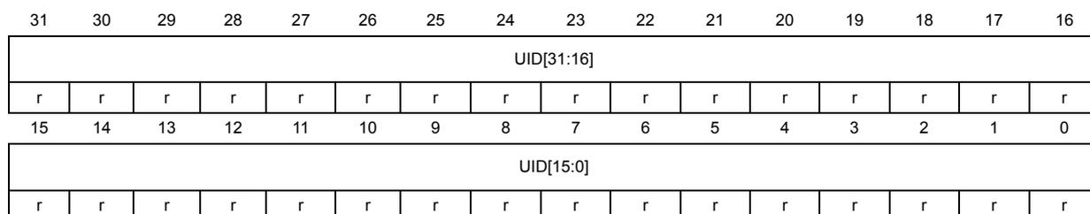
39.1 Unique device ID register (96 bits)
The unique device identifier is ideally suited:
- • for use as serial numbers (for example USB string serial numbers or other end applications)
- • for use as part of the security keys in order to increase the security of code in flash memory while using and combining this unique ID with software cryptographic primitives/ and protocols before programming the internal flash memory
- • to activate secure boot processes, etc.
The 96-bit unique device identifier provides a reference number which is unique for any device and in any context. These bits cannot be altered by the user.
Base address: 0x1FFF 6E50 (STM32U073/83xx), 0x1FFF 3E50 (STM32U031xx)
Address offset: 0x00
Reset value: 0xXXXX XXXX (where X is factory-programmed)
| 31 | 30 | 29 | 28 | 27 | 26 | 25 | 24 | 23 | 22 | 21 | 20 | 19 | 18 | 17 | 16 |
| UID[31:16] | |||||||||||||||
| r | r | r | r | r | r | r | r | r | r | r | r | r | r | r | r |
| 15 | 14 | 13 | 12 | 11 | 10 | 9 | 8 | 7 | 6 | 5 | 4 | 3 | 2 | 1 | 0 |
| UID[15:0] | |||||||||||||||
| r | r | r | r | r | r | r | r | r | r | r | r | r | r | r | r |
Bits 31:0 UID[31:0] : X and Y coordinates on the wafer expressed in BCD format
Address offset: 0x04
Reset value: 0xXXXX XXXX (where X is factory-programmed)
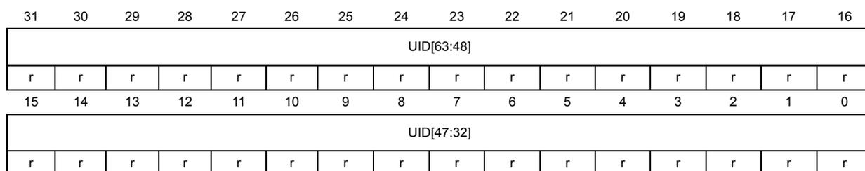
| 31 | 30 | 29 | 28 | 27 | 26 | 25 | 24 | 23 | 22 | 21 | 20 | 19 | 18 | 17 | 16 |
| UID[63:48] | |||||||||||||||
| r | r | r | r | r | r | r | r | r | r | r | r | r | r | r | r |
| 15 | 14 | 13 | 12 | 11 | 10 | 9 | 8 | 7 | 6 | 5 | 4 | 3 | 2 | 1 | 0 |
| UID[47:32] | |||||||||||||||
| r | r | r | r | r | r | r | r | r | r | r | r | r | r | r | r |
Bits 31:8 UID[63:40]: LOT_NUM[23:0]
Lot number (ASCII encoded)
Bits 7:0 UID[39:32]: WAF_NUM[7:0]
Wafer number (8-bit unsigned number)
Address offset: 0x08
Reset value: 0xXXXX XXXX where X is factory-programmed
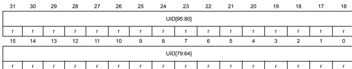
| 31 | 30 | 29 | 28 | 27 | 26 | 25 | 24 | 23 | 22 | 21 | 20 | 19 | 18 | 17 | 16 |
| UID[95:80] | |||||||||||||||
| r | r | r | r | r | r | r | r | r | r | r | r | r | r | r | r |
| 15 | 14 | 13 | 12 | 11 | 10 | 9 | 8 | 7 | 6 | 5 | 4 | 3 | 2 | 1 | 0 |
| UID[79:64] | |||||||||||||||
| r | r | r | r | r | r | r | r | r | r | r | r | r | r | r | r |
Bits 31:0 UID[95:64]: LOT_NUM[55:24]
Lot number (ASCII encoded)
39.2 Flash memory size data register
Base address: 0x1FFF 6EA0 (STM32U073/83xx), 0x1FFF 3EA0 (STM32U031xx)
Address offset: 0x00
Reset value: 0xXXXX where X is factory-programmed

| 15 | 14 | 13 | 12 | 11 | 10 | 9 | 8 | 7 | 6 | 5 | 4 | 3 | 2 | 1 | 0 |
| FLASH_SIZE | |||||||||||||||
| r | r | r | r | r | r | r | r | r | r | r | r | r | r | r | r |
Bits 15:0 FLASH_SIZE[15:0] : Flash memory size
This bitfield indicates the size of the device flash memory expressed in Kbytes.
As an example, 0x040 corresponds to 64 Kbytes.
39.3 Package data register
Base address: 0x1FFF 6D00 (STM32U073/83xx), 0x1FFF 3D00 (STM32U031xx)
Address offset: 0x00
Reset value: 0xXXXX where X is factory-programmed

| 15 | 14 | 13 | 12 | 11 | 10 | 9 | 8 | 7 | 6 | 5 | 4 | 3 | 2 | 1 | 0 |
| Res. | Res. | Res. | Res. | Res. | Res. | Res. | Res. | Res. | Res. | Res. | Res. | PKG[3:0] | |||
| r | r | r | r | ||||||||||||
Bits 15:4 Reserved
Bits 3:0 PKG[3:0] : Package type
Condition: STM32U031xx
0000 : Reserved
0001 : UFQFPN32
0011 : UFQFPN48
0100 : LQFP48
0101 : LQFP64
0110 : BGA64
1001 : TSSOP20
1010 : WLCSP29
1011 : LQFP32
Others: Reserved
Condition: STM32U0x3xx
0000 : Reserved
0001 : UFQFPN32
0010 : WLCSP42
0011 : UFQFPN48
0100 : LQFP48
0101 : LQFP64
0110 : BGA64
0111 : LQFP80
1000 : BGA81
Others : Reserved
Appendix A OEM key CRC calculation source code
Below is the source code that can be used to compare the result of the CRC computation performed on the loaded OEM1/2 keys (option byte loading or programming of new keys), with the CRC values of the OEM1/2 keys available in the OEM1KEYCRC/OEM2KEYCRC bitfields of the FLASH_OEMKEYSR register.
uint8_t getCRC(uint32_t * keyin)
{
    const uint8_t CRC7_POLY = 0x7;
    const uint32_t key_strobe[4] = {0xAA55AA55, 0x3, 0x18, 0xC0};
    uint8_t i, j, k, crc = 0x0;
    uint32_t keyval;

    for (j = 0; j < 4; j++)
    {
        keyval = *(keyin+j);
        if (j == 0)
        {
            keyval ^= key_strobe[0];
        } else
        {
            keyval ^= (key_strobe[j] << 24) | (crc << 16) | (key_strobe[j] << 8) |
            crc;
        }
        for (i = 0, crc = 0; i < 32; i++)
        {
            k = (((crc >> 7) ^ (keyval >> (31-i))&0xF)) & 1;
            crc <<= 1;
            if (k)
            {
                crc ^= CRC7_POLY;
            }
        }
        crc ^= 0x55;
    }
    return crc;
}
Important security notice
The STMicroelectronics group of companies (ST) places a high value on product security, which is why the ST product(s) identified in this documentation may be certified by various security certification bodies and/or may implement our own security measures as set forth herein. However, no level of security certification and/or built-in security measures can guarantee that ST products are resistant to all forms of attacks. As such, it is the responsibility of each of ST's customers to determine if the level of security provided in an ST product meets the customer needs both in relation to the ST product alone, as well as when combined with other components and/or software for the customer end product or application. In particular, take note that:
- • ST products may have been certified by one or more security certification bodies, such as Platform Security Architecture ( www.psacertified.org ) and/or Security Evaluation standard for IoT Platforms ( www.trustcb.com ). For details concerning whether the ST product(s) referenced herein have received security certification along with the level and current status of such certification, either visit the relevant certification standards website or go to the relevant product page on www.st.com for the most up to date information. As the status and/or level of security certification for an ST product can change from time to time, customers should re-check security certification status/level as needed. If an ST product is not shown to be certified under a particular security standard, customers should not assume it is certified.
- • Certification bodies have the right to evaluate, grant and revoke security certification in relation to ST products. These certification bodies are therefore independently responsible for granting or revoking security certification for an ST product, and ST does not take any responsibility for mistakes, evaluations, assessments, testing, or other activity carried out by the certification body with respect to any ST product.
- • Industry-based cryptographic algorithms (such as AES, DES, or MD5) and other open standard technologies which may be used in conjunction with an ST product are based on standards which were not developed by ST. ST does not take responsibility for any flaws in such cryptographic algorithms or open technologies or for any methods which have been or may be developed to bypass, decrypt or crack such algorithms or technologies.
- • While robust security testing may be done, no level of certification can absolutely guarantee protections against all attacks, including, for example, against advanced attacks which have not been tested for, against new or unidentified forms of attack, or against any form of attack when using an ST product outside of its specification or intended use, or in conjunction with other components or software which are used by customer to create their end product or application. ST is not responsible for resistance against such attacks. As such, regardless of the incorporated security features and/or any information or support that may be provided by ST, each customer is solely responsible for determining if the level of attacks tested for meets their needs, both in relation to the ST product alone and when incorporated into a customer end product or application.
- • All security features of ST products (inclusive of any hardware, software, documentation, and the like), including but not limited to any enhanced security features added by ST, are provided on an "AS IS" BASIS. AS SUCH, TO THE EXTENT PERMITTED BY APPLICABLE LAW, ST DISCLAIMS ALL WARRANTIES, EXPRESS OR IMPLIED, INCLUDING BUT NOT LIMITED TO THE IMPLIED WARRANTIES OF MERCHANTABILITY OR FITNESS FOR A PARTICULAR PURPOSE, unless the applicable written and signed contract terms specifically provide otherwise.
Revision history
Table 261. Document revision history
Table 261. Document revision history (continued)
| Date | Revision | Changes |
|---|---|---|
| 24-Jun-2025 | 3 (continued) | Section 5: Reset and clock control (RCC) Section 6: Clock recovery system (CRS) Section 7: General-purpose I/Os (GPIO) Section 8: System configuration controller (SYSCFG) Section 10: DMA request multiplexer (DMAMUX) |
Table 261. Document revision history (continued)
| Date | Revision | Changes |
|---|---|---|
| 24-Jun-2025 | 3 (continued) | Section 11: Nested vectored interrupt controller (NVIC) Section 12: Extended interrupt and event controller (EXTI) Section 14: Analog-to-digital converter (ADC) Section 15: Digital-to-analog converter (DAC) Section 17: Comparator (COMP) Section 19: Liquid crystal display controller (LCD) Section 21: True random number generator (RNG) Section 22: AES hardware accelerator (AES) |
Table 261. Document revision history (continued)
| Date | Revision | Changes |
|---|---|---|
| 24-Jun-2025 | 3 (continued) | Section 27: Low-power timer (LPTIM) |
Table 261. Document revision history (continued)
| Date | Revision | Changes |
|---|---|---|
| 24-Jun-2025 | 3 (continued) | Section 35: Low-power universal asynchronous receiver transmitter (LPUART) Removed introductory sentence. Updated Section 35.4.5: LPUART FIFOs and thresholds , Section 35.4.8: LPUART baud rate generation , Section : Transmission using DMA and Section : Reception using DMA . Removed table Error calculation for programmed baud rates at \( f_{CK} = 100 \) MHz . Replaced \( f_{ck} \) by lpuart_ker_ck_pres in and Section : RS485 driver enable and in LPUART baud rate register (LPUART_BRR) description. Updated description of the TE bit of the LPUART control register 1 (LPUART_CR1) and LPUART control register 1 [alternate] (LPUART_CR1) . Updated description of the TXFT and RXFT bits of the LPUART interrupt and status register (LPUART_ISR) . |
| 02-Jul-2025 | 4 | Updated document bookmarks. |
Index
A
| ADC_AWD1TR | 377 |
| ADC_AWD2CR | 381 |
| ADC_AWD2TR | 377 |
| ADC_AWD3CR | 382 |
| ADC_AWD3TR | 380 |
| ADC_CALFACT | 382 |
| ADC_CCR | 383 |
| ADC_CFGR1 | 371 |
| ADC_CFGR2 | 374 |
| ADC_CHSELR | 377-378 |
| ADC_CR | 369 |
| ADC_DR | 381 |
| ADC_IER | 367 |
| ADC_ISR | 366 |
| ADC_SMPR | 376 |
| AES_CR | 541 |
| AES_DINR | 544 |
| AES_DOUTR | 545 |
| AES_IVR0 | 547 |
| AES_IVR1 | 548 |
| AES_IVR2 | 548 |
| AES_IVR3 | 548 |
| AES_KEYR0 | 546 |
| AES_KEYR1 | 546 |
| AES_KEYR2 | 547 |
| AES_KEYR3 | 547 |
| AES_KEYR4 | 549 |
| AES_KEYR5 | 549 |
| AES_KEYR6 | 549 |
| AES_KEYR7 | 550 |
| AES_SR | 543 |
| AES_SUSPxR | 550 |
| AP0_CSW | 1261 |
| AP1_CSW | 1260 |
| APx_BASE | 1263 |
| APx_BDn | 1263 |
| APx_DRW | 1262 |
| APx_IDR | 1264 |
| APx_TAR | 1262 |
B
| BPU_CIDR0 | 1294 |
| BPU_CIDR1 | 1294 |
| BPU_CIDR2 | 1295 |
| BPU_CIDR3 | 1295 |
| BPU_COMPx | 1291 |
| BPU_CTRL | 1291 |
| BPU_PIDR0 | 1292 |
| BPU_PIDR1 | 1293 |
| BPU_PIDR2 | 1293 |
| BPU_PIDR3 | 1294 |
| BPU_PIDR4 | 1292 |
C
| C1ROM_CIDR3 | 1272, 1277, 1282 |
| COMP1_CSR | 421 |
| COMP2_CSR | 422 |
| CPURROM_CIDR0 | 1280 |
| CPURROM_CIDR1 | 1281 |
| CPURROM_CIDR2 | 1281 |
| CPURROM_CIDR3 | 1281 |
| CPURROM_MEMTYPE | 1278 |
| CPURROM_PIDR0 | 1279 |
| CPURROM_PIDR1 | 1279 |
| CPURROM_PIDR2 | 1279 |
| CPURROM_PIDR3 | 1280 |
| CPURROM_PIDR4 | 1278 |
| CRC_CR | 324 |
| CRC_DR | 323 |
| CRC_IDR | 323 |
| CRC_INIT | 325 |
| CRC_POL | 325 |
| CRS_CFGR | 220 |
| CRS_CR | 219 |
| CRS_ICR | 223 |
| CRS_ISR | 221 |
D
| DAC_CCR | 406 |
| DAC_CR | 401 |
| DAC_DHR12L1 | 404 |
| DAC_DHR12R1 | 403 |
| DAC_DHR8R1 | 404 |
| DAC_DOR1 | 405 |
| DAC_MCR | 406 |
| DAC_SHHR | 407 |
| DAC_SHRR | 408 |
| DAC_SHSR1 | 407 |
| DAC_SR | 405 |
| DAC_SWTRGR | 403 |
| DBGMCU_APB1FZR | 1306 |
| DBGMCU_APB2FZR | 1308 |
| DBGMCU_CIDR0 | 1313 |
| DBGMCU_CIDR1 | 1313 |
| DBGMCU_CIDR2 | 1314 |
| DBGMCU_CIDR3 | 1314 |
| DBGMCU_CR | 1305 |
| DBGMCU_DBG_AUTH_DEVICE | 1310 |
| DBGMCU_DBG_AUTH_HOST | 1309 |
| DBGMCU_IDCODE | 1305 |
| DBGMCU_PIDR0 | 1311 |
| DBGMCU_PIDR1 | 1311 |
| DBGMCU_PIDR2 | 1312 |
| DBGMCU_PIDR3 | 1312 |
| DBGMCU_PIDR4 | 1310 |
| DBGMCU_SR | 1309 |
| DMA_CCRx | 279 |
| DMA_CMARx | 283 |
| DMA_CNDTRx | 281 |
| DMA_CPARx | 282 |
| DMA_IFCR | 277 |
| DMA_ISR | 275 |
| DMAMUX_CFR | 297 |
| DMAMUX_CSR | 297 |
| DMAMUX_CxCR | 296 |
| DMAMUX_RGCFR | 299 |
| DMAMUX_RGS | 299 |
| DMAMUX_RGxCR | 298 |
| DP_ABORT | 1252 |
| DP_CTRLSTAT | 1253 |
| DP_DLCR | 1254 |
| DP_DLPIDR | 1255 |
| DP_PIDR | 1251 |
| DP_RDBUFF | 1256 |
| DP_RESEND | 1255 |
| DP_SELECT | 1256 |
| DP_TARGETID | 1254 |
| DWT_CIDR0 | 1287 |
| DWT_CIDR1 | 1288 |
| DWT_CIDR2 | 1288 |
| DWT_CIDR3 | 1288 |
| DWT_COMPx | 1284 |
| DWT_CTRL | 1283 |
| DWT_FUNCTIONx | 1285 |
| DWT_MASKx | 1284 |
| DWT_PCSR | 1284 |
| DWT_PIDR0 | 1286 |
| DWT_PIDR1 | 1286 |
| DWT_PIDR2 | 1286 |
| DWT_PIDR3 | 1287 |
| DWT_PIDR4 | 1285 |
| EXTI_EMR1 | 316 |
| EXTI_EMR2 | 317 |
| EXTI_EXTICRx | 315 |
| EXTI_FPR1 | 314 |
| EXTI_FTSR1 | 313 |
| EXTI_IMR1 | 316 |
| EXTI_IMR2 | 317 |
| EXTI_RPR1 | 314 |
| EXTI_RTSR1 | 312 |
| EXTI_SWIER1 | 313 |
| FLASH_ACR | 86 |
| FLASH_CR | 90 |
| FLASH_ECCR | 92 |
| FLASH_HDPCR | 100 |
| FLASH_HDPEXTR | 101 |
| FLASH_KEYR | 87 |
| FLASH_OEM1KEYR1 | 97 |
| FLASH_OEM1KEYR2 | 97 |
| FLASH_OEM1KEYR3 | 97 |
| FLASH_OEM1KEYR4 | 98 |
| FLASH_OEM2KEYR1 | 98 |
| FLASH_OEM2KEYR2 | 99 |
| FLASH_OEM2KEYR3 | 99 |
| FLASH_OEM2KEYR4 | 99 |
| FLASH_OEMKEYSR | 100 |
| FLASH_OPTKEYR | 87 |
| FLASH_OPTR | 93 |
| FLASH_SECR | 96 |
| FLASH_SR | 88 |
| FLASH_WRP1AR | 95 |
| FLASH_WRP1BR | 95 |
| GPIOx_AFRH | 240 |
| GPIOx_AFRL | 239 |
| GPIOx_BRR | 241 |
| GPIOx_BSRR | 237 |
| GPIOx_IDR | 237 |
| GPIOx_LCKR | 238 |
| GPIOx_MODER | 235 |
| GPIOx_ODR | 237 |
| GPIOx_OSPEEDR | 236 |
| GPIOx_OTYPER | 235 |
| GPIOx_PUPDR | 236 |
| I2C_CR1 | 1004 |
| I2C_CR2 | 1006 |
| I2C_ICR | 1013 |
| I2C_ISR | 1011 |
| I2C_OAR1 | 1008 |
| I2C_OAR2 | 1009 |
| I2C_RXDR | 1013 |
| I2C_TIMINGR | 1010 |
| I2C_TXDR | 1014 |
| IWDG_EWCR | 895 |
| IWDG_KR | 892 |
| IWDG_PR | 892 |
| IWDG_RLR | 893 |
| IWDG_SR | 893 |
| IWDG_WINR | 895 |
L
| LCD_CLR | 460 |
| LCD_CR | 456 |
| LCD_FCR | 457 |
| LCD_RAMx | 461-462 |
| LCD_SR | 459 |
| LPTIM_ARR | 869 |
| LPTIM_CCMR1 | 871 |
| LPTIM_CCMR2 | 874 |
| LPTIM_CCR1 | 868 |
| LPTIM_CCR2 | 876 |
| LPTIM_CCR3 | 877 |
| LPTIM_CCR4 | 878 |
| LPTIM_CFGR | 864 |
| LPTIM_CFGR2 | 869 |
| LPTIM_CNT | 869 |
| LPTIM_CR | 867 |
| LPTIM_RCR | 871 |
| LPTIMx_DIER | 860, 862 |
| LPTIMx_ICR | 857, 859 |
| LPTIMx_ISR | 852, 854 |
| LPUART_BRR | 1149 |
| LPUART_CR1 | 1136, 1139 |
| LPUART_CR2 | 1142 |
| LPUART_CR3 | 1144, 1147 |
| LPUART_ICR | 1158 |
| LPUART_ISR | 1150, 1155 |
| LPUART_PRESC | 1160 |
| LPUART_RDR | 1159 |
| LPUART_RQR | 1149 |
| LPUART_TDR | 1159 |
M
| MCUROM_CIDR0 | 1275 |
| MCUROM_CIDR1 | 1276 |
| MCUROM_CIDR2 | 1276 |
| MCUROM_CIDR3 | 1276 |
| MCUROM_MEMTYPER | 1273 |
| MCUROM_PIDR0 | 1274 |
| MCUROM_PIDR1 | 1274 |
| MCUROM_PIDR2 | 1274 |
| MCUROM_PIDR3 | 1275 |
| MCUROM_PIDR4 | 1273 |
O
| OPAMP1_CSR | 434 |
| OPAMP1_LPOTR | 435 |
| OPAMP1_OTR | 435 |
P
| PWR_CR1 | 132 |
| PWR_CR2 | 133 |
| PWR_CR3 | 134 |
| PWR_CR4 | 136 |
| PWR_PDCRA | 141 |
| PWR_PDCRB | 143 |
| PWR_PDCRC | 144 |
| PWR_PDCRD | 145 |
| PWR_PDCRE | 146 |
| PWR_PDCRF | 147 |
| PWR_PUCRA | 141 |
| PWR_PUCRB | 142 |
| PWR_PUCRC | 143 |
| PWR_PUCRD | 144 |
| PWR_PUCRE | 145 |
| PWR_PUCRF | 147 |
| PWR_SCR | 140 |
| PWR_SR1 | 137 |
| PWR_SR2 | 138 |
R
| RCC_AHBENR | 189 |
| RCC_AHBSTR | 182 |
| RCC_AHBSMENR | 196 |
| RCC_APBENR1 | 192 |
| RCC_APBENR2 | 195 |
| RCC_APBSTR1 | 185 |
| RCC_APBSTR2 | 188 |
| RCC_APBMSMENR1 | 198 |
| RCC_APBMSMENR2 | 202 |
| RCC_BDCR | 205 |
| RCC_CCIPR | 203 |
| RCC_CFGR | 173 |
| RCC_CICR | 181 |
| RCC_CIER | 178 |
| RCC_CIFR | 180 |
| RCC_CR | 169 |
| RCC_CRRCR | 209 |
| RCC_CSR | 207 | SYSCFG_ITLINE0 | 249 |
| RCC_DBGCFGR | 191 | SYSCFG_ITLINE1 | 249 |
| RCC_ICSCR | 172 | SYSCFG_ITLINE10 | 253 |
| RCC_IOPENR | 190 | SYSCFG_ITLINE11 | 254 |
| RCC_IOPRSTR | 184 | SYSCFG_ITLINE12 | 254 |
| RCC_IOPSMENR | 197 | SYSCFG_ITLINE13 | 255 |
| RCC_PLLCFGR | 176 | SYSCFG_ITLINE14 | 255 |
| RNG_CR | 498 | SYSCFG_ITLINE15 | 256 |
| RNG_DR | 501 | SYSCFG_ITLINE16 | 256 |
| RNG_HTCR | 502 | SYSCFG_ITLINE17 | 256 |
| RNG_NSCR | 502 | SYSCFG_ITLINE18 | 257 |
| RNG_SR | 500 | SYSCFG_ITLINE19 | 257 |
| RTC_ALRABINR | 944 | SYSCFG_ITLINE2 | 250 |
| RTC_ALRBBINR | 944 | SYSCFG_ITLINE20 | 257 |
| RTC_ALRMAR | 937 | SYSCFG_ITLINE21 | 258 |
| RTC_ALRMASSR | 938 | SYSCFG_ITLINE22 | 258 |
| RTC_ALRMBR | 939 | SYSCFG_ITLINE23 | 258 |
| RTC_ALRMBSSR | 940 | SYSCFG_ITLINE24 | 259 |
| RTC_CALR | 933 | SYSCFG_ITLINE25 | 259 |
| RTC_CR | 929 | SYSCFG_ITLINE26 | 259 |
| RTC_DR | 925 | SYSCFG_ITLINE27 | 260 |
| RTC_ICSR | 926 | SYSCFG_ITLINE28 | 260 |
| RTC_MISR | 942 | SYSCFG_ITLINE29 | 261 |
| RTC_PRER | 928 | SYSCFG_ITLINE3 | 250 |
| RTC_SCR | 943 | SYSCFG_ITLINE30 | 261 |
| RTC_SHIFTTR | 934 | SYSCFG_ITLINE31 | 261 |
| RTC_SR | 941 | SYSCFG_ITLINE4 | 251 |
| RTC_SSR | 926 | SYSCFG_ITLINE5 | 251 |
| RTC_TR | 924 | SYSCFG_ITLINE6 | 251 |
| RTC_TSDR | 936 | SYSCFG_ITLINE7 | 252 |
| RTC_TSSSR | 936 | SYSCFG_ITLINE8 | 252 |
| RTC_TSTR | 935 | SYSCFG_ITLINE9 | 253 |
| RTC_WPR | 933 | SYSCFG_SCSR | 247 |
| RTC_WUTR | 929 | SYSCFG_SKR | 248 |
| SYSCFG_TSCCR | 248 | ||
| S | SYROM_CIDR0 | 1270 | |
| SCS_DCRDR | 1301 | SYROM_CIDR1 | 1271 |
| SCS_DCRSR | 1300 | SYROM_CIDR2 | 1271 |
| SCS_DEMCR | 1302 | SYROM_CIDR3 | 1271 |
| SCS_DFSR | 1297 | SYROM_MEMTYPER | 1268 |
| SCS_DHCSR | 1298-1299 | SYROM_PIDR0 | 1269 |
| SCS_SHCSR | 1297 | SYROM_PIDR1 | 1269 |
| SPIx_CR1 | 1189 | SYROM_PIDR2 | 1269 |
| SPIx_CR2 | 1191 | SYROM_PIDR3 | 1270 |
| SPIx_CRCPR | 1195 | SYROM_PIDR4 | 1268 |
| SPIx_DR | 1194 | ||
| SPIx_RXCRCR | 1195 | T | |
| SPIx_SR | 1193 | TAMP_BKPxR | 966 |
| SPIx_TXCRCR | 1195 | TAMP_CR1 | 955 |
| SYSCFG_CFGR1 | 243 | TAMP_CR2 | 957 |
| SYSCFG_CFGR2 | 246 | TAMP_CR3 | 959 |
| TAMP_FLTCR | 960 | TIM16_ARR | 817 |
| TAMP_IER | 961 | TIM16_BDTR | 819 |
| TAMP_MISR | 963 | TIM16_CCER | 814 |
| TAMP_SCR | 965 | TIM16_CCMR1 | 811-812 |
| TAMP_SR | 962 | TIM16_CCR1 | 818 |
| TIM1_AF1 | 647 | TIM16_CNT | 816 |
| TIM1_AF2 | 648 | TIM16_CR1 | 806 |
| TIM1_ARR | 635 | TIM16_CR2 | 807 |
| TIM1_BDTR | 638 | TIM16_DCR | 822 |
| TIM1_CCER | 631 | TIM16_DIER | 808 |
| TIM1_CCMR1 | 625-626 | TIM16_DMAR | 822 |
| TIM1_CCMR2 | 629-630 | TIM16_EGR | 810 |
| TIM1_CCMR3 | 644 | TIM16_PSC | 817 |
| TIM1_CCR1 | 636 | TIM16_RCR | 818 |
| TIM1_CCR2 | 637 | TIM16_SR | 809 |
| TIM1_CCR3 | 637 | TIM16_TISEL | 824 |
| TIM1_CCR4 | 638 | TIM2_AF1 | 722 |
| TIM1_CCR5 | 645 | TIM2_OR1 | 721 |
| TIM1_CCR6 | 646 | TIM2_TISEL | 723 |
| TIM1_CNT | 635 | TIM3_AF1 | 722 |
| TIM1_CR1 | 614 | TIM3_OR1 | 721 |
| TIM1_CR2 | 615 | TIM3_TISEL | 723 |
| TIM1_DCR | 642 | TIMx_ARR | 718, 739 |
| TIM1_DIER | 620 | TIMx_CCER | 715 |
| TIM1_DMAR | 643 | TIMx_CCMR1 | 709, 711 |
| TIM1_EGR | 624 | TIMx_CCMR2 | 713-714 |
| TIM1_OR1 | 644 | TIMx_CCR1 | 718 |
| TIM1_PSC | 635 | TIMx_CCR2 | 718 |
| TIM1_RCR | 636 | TIMx_CCR3 | 719 |
| TIM1_SMCR | 618 | TIMx_CCR4 | 719 |
| TIM1_SR | 622 | TIMx_CNT | 716-717, 738 |
| TIM1_TISEL | 650 | TIMx_CR1 | 699, 735 |
| TIM15_AF1 | 802 | TIMx_CR2 | 700, 737 |
| TIM15_ARR | 796 | TIMx_DCR | 720 |
| TIM15_BDTR | 798 | TIMx_DIER | 705, 737 |
| TIM15_CCER | 793 | TIMx_DMAR | 721 |
| TIM15_CCMR1 | 789-790 | TIMx_EGR | 708, 738 |
| TIM15_CCR1 | 797 | TIMx_PSC | 717, 739 |
| TIM15_CCR2 | 798 | TIMx_SMCR | 702 |
| TIM15_CNT | 796 | TIMx_SR | 706, 738 |
| TIM15_CR1 | 781 | TSC_CR | 477 |
| TIM15_CR2 | 782 | TSC_ICR | 481 |
| TIM15_DCR | 801 | TSC_IER | 480 |
| TIM15_DIER | 785 | TSC_IOASCR | 482 |
| TIM15_DMAR | 801 | TSC_IOCCR | 483 |
| TIM15_EGR | 788 | TSC_IOGCSR | 484 |
| TIM15_PSC | 796 | TSC_IOGxCR | 484 |
| TIM15_RCR | 797 | TSC_IOHCR | 482 |
| TIM15_SMCR | 784 | TSC_IOSCR | 483 |
| TIM15_SR | 786 | TSC_ISR | 481 |
| TIM15_TISEL | 803 | ||
| TIM16_AF1 | 823 |
| USART_BRR ..... | 1087 |
| USART_CR1 ..... | 1068, 1072 |
| USART_CR2 ..... | 1075 |
| USART_CR3 ..... | 1079, 1083 |
| USART_GTPR ..... | 1087 |
| USART_ICR ..... | 1101 |
| USART_ISR ..... | 1090, 1096 |
| USART_PRESC ..... | 1103 |
| USART_RDR ..... | 1102 |
| USART_RQR ..... | 1089 |
| USART_RTOR ..... | 1088 |
| USART_TDR ..... | 1103 |
| USB_BCDR ..... | 1229 |
| USB_CHEP_RXTXBD_n ..... | 1243-1244 |
| USB_CHEP_TXRXBD_n ..... | 1241 |
| USB_CHEPnR ..... | 1230 |
| USB_CNTR ..... | 1220 |
| USB_DADDR ..... | 1227 |
| USB_FNR ..... | 1227 |
| USB_ISTR ..... | 1223 |
| USB_LPMCSR ..... | 1228 |
| VREFBUF_CCR ..... | 413 |
| VREFBUF_CSR ..... | 412 |
| WWDG_CFR ..... | 903 |
| WWDG_CR ..... | 902 |
| WWDG_SR ..... | 903 |
IMPORTANT NOTICE – READ CAREFULLY
STMicroelectronics NV and its subsidiaries (“ST”) reserve the right to make changes, corrections, enhancements, modifications, and improvements to ST products and/or to this document at any time without notice. Purchasers should obtain the latest relevant information on ST products before placing orders. ST products are sold pursuant to ST’s terms and conditions of sale in place at the time of order acknowledgment.
Purchasers are solely responsible for the choice, selection, and use of ST products and ST assumes no liability for application assistance or the design of purchasers' products.
No license, express or implied, to any intellectual property right is granted by ST herein.
Resale of ST products with provisions different from the information set forth herein shall void any warranty granted by ST for such product.
ST and the ST logo are trademarks of ST. For additional information about ST trademarks, refer to www.st.com/trademarks . All other product or service names are the property of their respective owners.
Information in this document supersedes and replaces information previously supplied in any prior versions of this document.
© 2025 STMicroelectronics – All rights reserved