38. Debug support (DBG)
38.1 Introduction
A limited set of debug features is provided to support software development and system integration:
- • Breakpoint debugging of the CPU core
The debug features can be controlled via a serial-wire debug access port, using industry standard debugging tools. The debug features are based on Arm® CoreSight™ components:
- • SWJ-DP: JTAG/Serial-wire debug port
- • AHB-AP: AHB access port
- • APB-AP: APB access port
- • ROM table
- • System control space (SCS)
- • Breakpoint unit (BPU)
- • Data watchpoint and trace unit (DWT)
The debug features are accessible by the debugger via the access ports.
Additional information can be found in the Arm documents referenced in Section 38.10: Reference documents .
Note: Only nonsecure memory access is supported in this product.
38.2 DBG functional description
38.2.1 DBG block diagram
Figure 386. Block diagram of debug support infrastructure
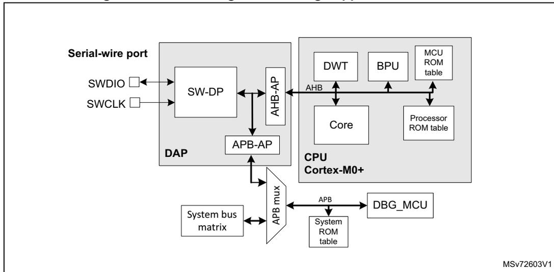
The diagram illustrates the debug support infrastructure. On the left, a 'Serial-wire port' with pins SWDIO and SWCLK is connected to a 'SW-DP' block. The 'SW-DP' block is part of a 'DAP' (Debug Access Port) which also contains 'AHB-AP' and 'APB-AP' blocks. The 'DAP' is connected to a 'System bus matrix'. The 'System bus matrix' is connected to an 'APB mux', which in turn is connected to a 'System ROM table' and a 'DBG_MCU' block. The 'APB mux' is also connected to the 'APB-AP' block of the 'DAP'. The 'AHB-AP' block of the 'DAP' is connected to a 'CPU Cortex-M0+' block. The 'CPU Cortex-M0+' block contains a 'Core', 'DWT', 'BPU', 'MCU ROM table', and 'Processor ROM table'. The 'Core' is connected to the 'AHB' bus, which is also connected to the 'DWT', 'BPU', 'MCU ROM table', and 'Processor ROM table' blocks.
MSV72603V1
38.2.2 DBG pins and internal signals
SWD port pins
Two pins are used as outputs for the SW-DP as alternate functions of general purpose I/Os. These pins are available on all packages.
Table 239. SW debug port pins
| SW-DP pin name | SW debug port | Pin assignment | |
|---|---|---|---|
| Type | Debug assignment | ||
| SWDIO | I/O | Serial wire data input/output | PA13 |
| SWCLK | I | Serial wire clock | PA14 |
SW-DP pin assignment
After reset (SYSRESETn or PORESETn), the pins used for the SW-DP are assigned as dedicated pins, which are immediately usable by the debugger host.
However, the MCU offers the possibility to disable the SWD port, and can then release the associated pins for general-purpose I/O (GPIO) usage. For more details on how to disable SW-DP port pins, refer to Section 7.3.2: I/O pin alternate function multiplexer and mapping on page 228 .
Internal pull-up and pull-down on SWD pins
Once the SWD port is released by the user software, the GPIO controller takes control of these pins. The reset state of the GPIO control registers puts the I/Os in the following states:
- • SWDIO: input pull-up
- • SWCLK: input pull-down
Note: Having embedded pull-up and pull-down resistors removes the need to add external resistors.
38.2.3 ID codes and locking mechanism
There are several ID codes inside the MCU. ST strongly recommends tool manufacturers to lock their debugger using the MCU device ID located in the DBGMCU (see Section : DBGMCU device ID code register (DBGMCU_IDCODE) ).
Only the DEV_ID[11:0] field should be used for identification by the debugger/programmer tools (the REV_ID[15:0] field must not be taken into account).
38.2.4 DBG reset and clocks
The debug port (SW-DP) is reset by a power-on reset and when waking up from standby mode.
The debugger supplies the clock for the debug port via the debug interface pin SWCLK. This clock is used to register the serial input data in, as well as to operate the state machines and internal logic of the debug port. This clock must therefore continue to toggle for several cycles after the end of an access, to ensure that the debug port returns to the idle state.
The SW-DP contains an asynchronous interface to the system clock domain that covers the rest of the SW-DP and the access port.
The debug clock domain is enabled by the debugger using the CDBGPWRUPREQ bit in the DP control and status register (DP_CTRLSTAT) . The clock must be enabled before the debugger can access any of the debug features on the device. The availability of the clock is reflected in the CDBGPWRUPACK bit in DP_CTRLSTAT. The debug clock is disabled at power-up, and should be disabled before the debugger is disconnected, to avoid wasting energy.
The debug and trace components included in the processor are clocked with the processor clock.
38.2.5 DBG power domains
The debug components are located in the core power domain. This means that the debugger connection is not possible in standby low-power mode. To avoid losing the connection when the device enters standby mode, the power can be maintained to the core by setting a bit in the DBGMCU configuration register (DBGMCU_CR) . This also keeps the processor clocks active, and holds off the reset, so that the debug session is maintained.
38.2.6 Debug in low-power modes
The devices include power saving features that allow the core power domain to be switched off or stopped when not required. If the power is switched off or if the core is not clocked, all debug components are inaccessible to the debugger. To avoid this, power-saving mode emulation is implemented. If the emulation is enabled for a domain, the domain still enters power-saving mode, but its clock and power are maintained. In other words, the domain behaves as if it is in power-saving mode, but the debugger does not lose the connection.
The emulation mode is programmed in the microcontroller debug (DBGMCU) unit. For more information, refer to Section 38.9: Microcontroller debug unit (DBGMCU) .
38.2.7 Security
The trace and debug components allow a high degree of access to the processor and system during product development. In order to protect user code and ensure that the debug features cannot be used to alter or compromise the normal operation of the finished product, these features can be disabled or limited in scope. Debugger access is disabled while the processor is booting from system flash memory.
The following authentication signal is used by the system to determine which debug features are enabled or disabled:
- •
dbgen
: global enable for all debug features
- 0: All debug features are disabled.
- 1: Debug features are enabled.
For detailed information on the behavior of each component according to the state of the authentication signals, refer to the relevant component chapter or to the relevant Arm® technical documentation.
The state of the signals is set according to the debug state as shown in Table 240 .
Table 240. Authentication signal states
| Debug state | Authentication signal state | Description |
|---|---|---|
| OPEN | dbgen = 1 | Debug is enabled. All memory and resources are accessible to the debugger. |
| CLOSED | dbgen = 0 | Debug is disabled. |
The debug state depends on the flash memory readout protection state (see Section 3.5.1: FLASH read protection (RDP) ).
Table 241. Life cycle state and debug states
| Product readout protection state (RDP) (1) | Debug state |
|---|---|
| Level 0 | OPEN |
| Level 1 | CLOSED |
| Level 2 | CLOSED |
1. On new products, the readout protection mechanism is named “product life cycle”.
38.3 Serial-wire debug port (SW-DP)
The SW-DP is a CoreSight™ component that implements a two-pin (clock + data) serial-wire debug port for connecting debugging equipment.
A debugger must first select the SW-DP by transmitting the following serial data sequence on SWDIO:
... (50 or more ones) ..., 0, 1, 1, 1, 1, 0, 0, 1, 1, 1, 1, 0, 0, 1, 1, 1, ... (50 or more ones) ...
SWCLK must be cycled for each data bit.
38.3.1 Serial-wire debug port
The serial-wire debug protocol uses the following pins:
- • SWCLK: clock from host to target
- • SWDIO: bidirectional serial data
Serial data is transferred LSB first, synchronously with the clock.
A transfer comprises three phases:
- 1. Packet request (8 bits) transmitted by the host (see Table 242 ).
- 2. Acknowledge response (3 bits) transmitted by the target (see Table 243 ).
- 3. Data transfer (33 bits) transmitted by the host (in case of a write) or target (in case of a read) (see Table 244 ).
The data transfer only occurs if the acknowledge response is OK.
Between each phase, if the direction of the data is reversed, a single clock-cycle turn-around time is inserted.
Table 242. Packet request
| Bit field | Name | Description |
|---|---|---|
| 0 | Start | Must be 1 |
| 1 | APnDP | – 0: DP register access (see
Section 38.3.2: Debug port registers
) – 1: AP register access (see Section 38.4: Access ports ) |
| 2 | RnW | – 0: write request – 1: read request |
| 4:3 | A(3:2) | Address field of the DP or AP register (refer to Table 246 or Table 248 ) |
| 5 | Parity | Single bit parity of preceding bits |
| 6 | Stop | 0 |
| 7 | Park | Not driven by host, must be read as 1 by target |
Table 243. ACK response
| Bit field | Name | Description |
|---|---|---|
| 2:0 | ACK | – 000: FAULT – 010: WAIT – 100: OK |
Table 244. Data transfer
| Bit field | Name | Description |
|---|---|---|
| 31:0 | WDATA or RDATA | Write or read data |
| 32 | Parity | Single-bit parity of 32 data bits |
In the case of a FAULT or WAIT ACK response from the target, the data transfer phase is canceled, unless overrun detection is enabled: in this case, the data is ignored by the target (in the case of a write), or not driven (in the case of a read).
A line reset must be generated by the host when it is first connected, or following a protocol error. The line reset consists in 50 or more SWCLK cycles with SWDIO high, followed by two SWCLK cycles with SWDIO low.
For more details on the serial-wire debug protocol, refer to the Arm® Debug Interface Architecture Specification [ 11 ].
Note: The SWJ-DP implements SWD protocol version 2.
38.3.2 Debug port registers
The SW-DP accesses the debug port (DP) registers listed in Table 246 .
The debugger can access the DP registers as follows:
- 1. The A(3:2) and RnW fields are part of the packet request word sent to the SW-DP with the APnDP bit reset (see Table 242 ). Program the A(3:2) field with the register address (two most significant bits, the two LSBs are implicitly zero). Program the RnW bit to
select a read or write. In the case of a write, program the data field with the write data. The write data are sent in the data phase.
- To access one of the banked DP registers at address 0x4, the register number must first be written to the DPBANKSEL[3:0] field of the DP_SELECT register at address 0x8. Any subsequent read or write to address 0x4 accesses the register corresponding to the contents of DPBANKSEL.
Table 245. Debug port registers
| Address | A(3:2) value | R/W | Description |
|---|---|---|---|
| 0x0 | 00 | R | DP debug port identification register (DP_DPIDR) contains the IDCODE for the debug port. |
| W | DP abort register (DP_ABORT) aborts the current AP transaction. This register is also used to clear the error flags in the DP_CTRLSTATR register. | ||
| 0x4 | 01 | R/W | If DP_SELECTR.DPBANKSEL[3:0] = 0x0, DP control and status register (DP_CTRLSTAT) controls the DP and provides status information. |
| If DP_SELECTR.DPBANKSEL[3:0] = 0x1, DP data link control register (DP_DLCR) controls the operating mode of the SWD data link. | |||
| If DP_SELECTR.DPBANKSEL[3:0] = 0x2, DP target identification register (DP_TARGETID) provides target identification information. | |||
| If DP_SELECTR.DPBANKSEL[3:0] = 0x3, DP data link protocol identification register (DP_DLPIDR) provides the SWD protocol version. | |||
| 0x8 | 10 | R | DP event status register (DP_RESEND) returns the value that was returned by the last AP read or DP_RDBUFF read. Used in the event of a corrupted read transfer. |
| W | DP access port select register (DP_SELECT) selects the access port, access port register bank, and DP register at address 0x4. | ||
| 0xC | 11 | R | DP read buffer register (DP_RDBUFF) contains the result of the preceding AP read access, allowing a new AP access to be avoided. |
38.3.3 DEBUG port registers
DP debug port identification register (DP_DPIDR)
Address offset: 0x0
Reset value: 0x6BA0 2477
| 31 | 30 | 29 | 28 | 27 | 26 | 25 | 24 | 23 | 22 | 21 | 20 | 19 | 18 | 17 | 16 |
|---|---|---|---|---|---|---|---|---|---|---|---|---|---|---|---|
| REVISION[3:0] | PARTNO[7:0] | Res. | Res. | Res. | MIN | ||||||||||
| r | r | r | r | r | r | r | r | r | r | r | r | r | |||
| 15 | 14 | 13 | 12 | 11 | 10 | 9 | 8 | 7 | 6 | 5 | 4 | 3 | 2 | 1 | 0 |
| VERSION[3:0] | DESIGNER[10:0] | Res. | |||||||||||||
| r | r | r | r | r | r | r | r | r | r | r | r | r | r | r | |
- Bits 31:28
REVISION[3:0]
: revision code
0x6: Rev 6 - Bits 27:20
PARTNO[7:0]
: part number for the debug port
0xBA - Bits 19:17 Reserved, must be kept at reset value.
- Bit 16
MIN
: minimal debug port (MINDP) implementation
0x0: MINDP not implemented
- Bit 16
MIN
: minimal debug port (MINDP) implementation
- Bits 15:12
VERSION[3:0]
: debug port architecture version
0x2: DPv2 - Bits 11:1
DESIGNER[10:0]
: JEDEC designer identity code
0x23B: Arm® JEDEC code - Bit 0 Reserved, must be kept at reset value.
DP abort register (DP_ABORT)
Address offset: 0x0
Reset value: 0x0000 0000
| 31 | 30 | 29 | 28 | 27 | 26 | 25 | 24 | 23 | 22 | 21 | 20 | 19 | 18 | 17 | 16 |
|---|---|---|---|---|---|---|---|---|---|---|---|---|---|---|---|
| Res. | Res. | Res. | Res. | Res. | Res. | Res. | Res. | Res. | Res. | Res. | Res. | Res. | Res. | Res. | Res. |
| 15 | 14 | 13 | 12 | 11 | 10 | 9 | 8 | 7 | 6 | 5 | 4 | 3 | 2 | 1 | 0 |
| Res. | Res. | Res. | Res. | Res. | Res. | Res. | Res. | Res. | Res. | Res. | ORUNERRCLR | WDERRCLR | STKERRCLR | Res. | DAPABORT |
| w | w | w | w |
- Bits 31:5 Reserved, must be kept at reset value.
- Bit 4
ORUNERRCLR
: overrun error clear
- 0: no effect
- 1: STICKYORUN bit cleared in DP_CTRLSTAT register
- Bit 3
WDERRCLR
: write data error clear
- 0: no effect
- 1: WDATAERR bit cleared in DP_CTRLSTAT register
- Bit 2
STKERRCLR
: sticky error clear
- 0: no effect
- 1: STICKYERR bit cleared in DP_CTRLSTAT register
- Bit 1 Reserved, must be kept at reset value.
- Bit 0
DAPABORT
: current AP transaction aborted if excessive number of WAIT responses returned
This bit indicates that the transaction is stalled.- 0: no effect
- 1: transaction aborted
DP control and status register (DP_CTRLSTAT)
Address offset: 0x4
Reset value: 0x0000 0000
This register is accessible when DP_SELECT.DPBANKSEL[3:0] = 0x0.
| 31 | 30 | 29 | 28 | 27 | 26 | 25 | 24 | 23 | 22 | 21 | 20 | 19 | 18 | 17 | 16 |
|---|---|---|---|---|---|---|---|---|---|---|---|---|---|---|---|
| Res. | Res. | CDBGPWRUPACK | CDBGPWRUPREQ | Res. | Res. | Res. | Res. | Res. | Res. | Res. | Res. | Res. | Res. | Res. | Res. |
| r | r | ||||||||||||||
| 15 | 14 | 13 | 12 | 11 | 10 | 9 | 8 | 7 | 6 | 5 | 4 | 3 | 2 | 1 | 0 |
| Res. | Res. | Res. | Res. | Res. | Res. | Res. | Res. | WDATAERR | READOK | STICKYERR | Res. | Res. | Res. | STICKYORUN | ORUNDETECT |
| r | r | r | r | r |
Bits 31:30 Reserved, must be kept at reset value.
Bit 29 CDBGPWRUPACK : debug power-up acknowledge
See description in Section 38.2.6: Debug in low-power modes .
0: debug clock gated
1: debug clock enabled
Bit 28 CDBGPWRUPREQ : debug power-up request
This bit controls the debug clock enable.
0: requests debug clock gating
1: requests debug clock enable
Bits 27:8 Reserved, must be kept at reset value.
Bit 7 WDATAERR : write data error (read-only)
This bit indicates that there is a parity or framing error on the data phase of a write, or a write accepted by the DP is then discarded without being submitted to the AP.
This bit is reset by writing 1 to the DP_ABORT.WDERRCLR bit.
0: no error
1: an error occurred
Bit 6 READOK : AP read response (read-only)
This bit indicates the response to the last AP read access.
0: read not OK
1: read OK
Bit 5 STICKYERR : transaction error
This bit indicates that an error occurred in an AP transaction. It is reset by writing 1 to the DP_ABORT.STKERRCLR bit
0: no error
1: an error occurred
Bits 4:2 Reserved, must be kept at reset value.
Bit 1 STICKYORUN : overrun (read-only).
This bit indicates that an overrun occurred (new transaction received before previous transaction completed). This bit is only set if the ORUNDETECT bit is set. It is reset by writing 1 to the DP_ABORT.ORUNERRCLR bit.
0: no overrun
1: an overrun occurred
Bit 0 ORUNDETECT : overrun detection mode enable.
0: disabled
1: enabled. In the event of an overrun, the STICKYORUN bit is set and subsequent transactions are blocked until the STICKYORUN bit is cleared.
DP data link control register (DP_DLCR)
Address offset: 0x4
Reset value: 0x0000 0000
This register is accessible when DP_SELECT.DPBANKSEL[3:0] = 0x1.
| 31 | 30 | 29 | 28 | 27 | 26 | 25 | 24 | 23 | 22 | 21 | 20 | 19 | 18 | 17 | 16 |
|---|---|---|---|---|---|---|---|---|---|---|---|---|---|---|---|
| Res. | Res. | Res. | Res. | Res. | Res. | Res. | Res. | Res. | Res. | Res. | Res. | Res. | Res. | Res. | Res. |
| 15 | 14 | 13 | 12 | 11 | 10 | 9 | 8 | 7 | 6 | 5 | 4 | 3 | 2 | 1 | 0 |
| Res. | Res. | Res. | Res. | Res. | Res. | TURNROUND[1:0] | WIREMODE[1:0] | Res. | Res. | Res. | Res. | Res. | Res. | ||
| r | r | r | r | ||||||||||||
Bits 31:10 Reserved, must be kept at reset value.
Bits 9:8
TURNROUND[1:0]
: tristate period for SWDIO
0x0: 1 data bit period
Bits 7:6
WIREMODE[1:0]
: SW-DP mode
0x0: synchronous mode
Bits 5:0 Reserved, must be kept at reset value.
DP target identification register (DP_TARGETID)
Address offset: 0x4
Reset value: 0xXXXX 0041
This register is accessible when DP_SELECT.DPBANKSEL[3:0] = 0x2.
| 31 | 30 | 29 | 28 | 27 | 26 | 25 | 24 | 23 | 22 | 21 | 20 | 19 | 18 | 17 | 16 |
|---|---|---|---|---|---|---|---|---|---|---|---|---|---|---|---|
| TREVISION[3:0] | TPARTNO[15:4] | ||||||||||||||
| r | r | r | r | r | r | r | r | r | r | r | r | r | r | r | r |
| 15 | 14 | 13 | 12 | 11 | 10 | 9 | 8 | 7 | 6 | 5 | 4 | 3 | 2 | 1 | 0 |
| TPARTNO[3:0] | TDESIGNER[10:0] | Res. | |||||||||||||
| r | r | r | r | r | r | r | r | r | r | r | r | r | r | r | |
Bits 31:28 TREVISION[3:0] : target revision
Bits 27:12 TPARTNO[15:0] : target part number
0x4890: STM32U073/083x
0x4590: STM32U031x
Bits 11:1 TDESIGNER[10:0] : target designer JEDEC code
0x020: STMicroelectronics
Bit 0 Reserved, must be kept at reset value.
DP data link protocol identification register (DP_DLPIDR)
Address offset: 0x4
Reset value: 0x0000 0001
This register is accessible when DP_SELECTR.DPBANKSEL[3:0] = 0x3.
| 31 | 30 | 29 | 28 | 27 | 26 | 25 | 24 | 23 | 22 | 21 | 20 | 19 | 18 | 17 | 16 |
|---|---|---|---|---|---|---|---|---|---|---|---|---|---|---|---|
| TINSTANCE[3:0] | Res. | Res. | Res. | Res. | Res. | Res. | Res. | Res. | Res. | Res. | Res. | Res. | |||
| r | r | r | r | ||||||||||||
| 15 | 14 | 13 | 12 | 11 | 10 | 9 | 8 | 7 | 6 | 5 | 4 | 3 | 2 | 1 | 0 |
| Res. | Res. | Res. | Res. | Res. | Res. | Res. | Res. | Res. | Res. | Res. | Res. | PROTSVN[3:0] | |||
| r | r | r | r | ||||||||||||
Bits 31:28 TINSTANCE[3:0] : target instance number
This field defines the instance number for the device in a multi-drop system.
0x0: instance number 0
Bits 27:4 Reserved, must be kept at reset value.
Bits 3:0 PROTSVN[3:0] : Serial-wire debug protocol version
0x1: version 2
DP event status register (DP_RESEND)
Address offset: 0x8
Reset value: 0x0000 0000
| 31 | 30 | 29 | 28 | 27 | 26 | 25 | 24 | 23 | 22 | 21 | 20 | 19 | 18 | 17 | 16 |
|---|---|---|---|---|---|---|---|---|---|---|---|---|---|---|---|
| RESEND[31:16] | |||||||||||||||
| r | r | r | r | r | r | r | r | r | r | r | r | r | r | r | r |
| 15 | 14 | 13 | 12 | 11 | 10 | 9 | 8 | 7 | 6 | 5 | 4 | 3 | 2 | 1 | 0 |
| RESEND[15:0] | |||||||||||||||
| r | r | r | r | r | r | r | r | r | r | r | r | r | r | r | r |
Bits 31:0 RESEND[31:0] : value returned by the last AP read or DP_RDBUFF read
This register is used in the event of a corrupted read transfer.
DP access port select register (DP_SELECT)
Address offset: 0x8
Reset value: 0xXXXX XXXX
| 31 | 30 | 29 | 28 | 27 | 26 | 25 | 24 | 23 | 22 | 21 | 20 | 19 | 18 | 17 | 16 |
|---|---|---|---|---|---|---|---|---|---|---|---|---|---|---|---|
| APSEL[7:0] | Res. | Res. | Res. | Res. | Res. | Res. | Res. | Res. | |||||||
| w | w | w | w | w | w | w | w | ||||||||
| 15 | 14 | 13 | 12 | 11 | 10 | 9 | 8 | 7 | 6 | 5 | 4 | 3 | 2 | 1 | 0 |
| Res. | Res. | Res. | Res. | Res. | Res. | Res. | Res. | APBANKSEL[3:0] | DPBANKSEL[3:0] | ||||||
| w | w | w | w | w | w | w | w | ||||||||
Bits 31:24 APSEL[7:0] : access port select
This field selects the access port for the next transaction.
0x00: AP0 - System debug access port (APB-AP)
0x01: AP1 - Cortex ® -M0+ debug access port (AHB-AP)
others: reserved, must not be used
Bits 23:8 Reserved, must be kept at reset value.
Bits 7:4 APBANKSEL[3:0] : AP register bank select
This field selects the 4-word register bank on the active AP for the next transaction.
Bits 3:0 DPBANKSEL[3:0] : DP register bank select
This field selects the register at address 0x4 of the debug port.
0x0: DP_CTRLSTAT register
0x1: DP_DLCR register
0x2: DP_TARGETID register
0x3: DP_DLPIDR register
others: reserved, must not be used
DP read buffer register (DP_RDBUFF)
Address offset: 0xC
Reset value: 0x0000 0000
| 31 | 30 | 29 | 28 | 27 | 26 | 25 | 24 | 23 | 22 | 21 | 20 | 19 | 18 | 17 | 16 |
|---|---|---|---|---|---|---|---|---|---|---|---|---|---|---|---|
| RDBUFF[31:16] | |||||||||||||||
| r | r | r | r | r | r | r | r | r | r | r | r | r | r | r | r |
| 15 | 14 | 13 | 12 | 11 | 10 | 9 | 8 | 7 | 6 | 5 | 4 | 3 | 2 | 1 | 0 |
| RDBUFF[15:0] | |||||||||||||||
| r | r | r | r | r | r | r | r | r | r | r | r | r | r | r | r |
Bits 31:0 RDBUFF[31:0] : value returned by the last AP read access
The value returned by an AP read access can either be obtained using a second read access to the same address that initiates a new transaction on the corresponding bus, or else it can be read from this register, in which case no new AP transaction occurs.
38.3.4 Debug port register map and reset values
These registers are not on the CPU memory bus. They are only accessed through the SW-DP debug interface.
The debug port address offset is four-bit wide, where the two most significant bits are defined by the SW-DP packet request A[3:2] field. The two least significant bits are 00.
Table 246. Debug port register map and reset values
| Offset | Register name | 31 | 30 | 29 | 28 | 27 | 26 | 25 | 24 | 23 | 22 | 21 | 20 | 19 | 18 | 17 | 16 | 15 | 14 | 13 | 12 | 11 | 10 | 9 | 8 | 7 | 6 | 5 | 4 | 3 | 2 | 1 | 0 | |
|---|---|---|---|---|---|---|---|---|---|---|---|---|---|---|---|---|---|---|---|---|---|---|---|---|---|---|---|---|---|---|---|---|---|---|
| 0x0 | DP_PIDR | REVISION [3:0] | PARTNO[7:0] | Res. | Res. | Res. | MIN | VERSION [3:0] | DESIGNER[10:0] | Res. | ||||||||||||||||||||||||
| Reset value | 0 | 1 | 1 | 0 | 1 | 0 | 1 | 1 | 1 | 0 | 1 | 0 | 0 | 0 | 0 | 1 | 0 | 0 | 1 | 0 | 0 | 0 | 1 | 1 | 1 | 0 | 1 | 1 | 1 | |||||
| 0x0 | DP_ABORT | Res. | Res. | Res. | Res. | Res. | Res. | Res. | Res. | Res. | Res. | Res. | Res. | Res. | Res. | Res. | Res. | Res. | Res. | Res. | Res. | Res. | Res. | Res. | Res. | Res. | Res. | Res. | Res. | Res. | Res. | Res. | Res. | Res. |
| Reset value | ||||||||||||||||||||||||||||||||||
| 0x4 (1) | DP_CTRLSTAT | Res. | Res. | CDPGPWURUPACK | CDPGPWURUPREQ | Res. | Res. | Res. | Res. | Res. | Res. | Res. | Res. | Res. | Res. | Res. | Res. | Res. | Res. | Res. | Res. | Res. | Res. | Res. | Res. | WDATAERR | READOK | STICKYERR | Res. | Res. | Res. | Res. | Res. | |
| Reset value | 0 | 0 | 0 | 0 | 0 | |||||||||||||||||||||||||||||
| 0x4 (2) | DP_DLCR | Res. | Res. | Res. | Res. | Res. | Res. | Res. | Res. | Res. | Res. | Res. | Res. | Res. | Res. | Res. | Res. | Res. | Res. | Res. | Res. | Res. | Res. | TURNROUND[1:0] | WIREDMODE[1:0] | Res. | Res. | Res. | Res. | Res. | Res. | Res. | Res. | |
| Reset value | 0 | 0 | 0 | 0 | ||||||||||||||||||||||||||||||
| 0x4 (3) | DP_TARGETID | TREVSION [3:0] | TPARTNO[15:0] | Res. | ||||||||||||||||||||||||||||||
| Reset value | X | X | X | X | X | X | X | X | X | X | X | X | X | X | X | X | 0 | 0 | 0 | 0 | 0 | 0 | 0 | 0 | 0 | 0 | 1 | 0 | 0 | 0 | 0 | 0 | ||
| 0x4 (4) | DP_DLPID | TINSTANCE[3:0] | Res. | Res. | Res. | Res. | Res. | Res. | Res. | Res. | Res. | Res. | Res. | Res. | Res. | Res. | Res. | Res. | Res. | Res. | Res. | Res. | Res. | Res. | Res. | Res. | Res. | Res. | Res. | Res. | PROTSVN[3:0] | Res. | ||
| Reset value | 0 | 0 | 0 | 0 | 0 | 0 | 0 | 1 | ||||||||||||||||||||||||||
| 0x8 | DP_RESEND | RESEND[31:0] | ||||||||||||||||||||||||||||||||
| Reset value | 0 | 0 | 0 | 0 | 0 | 0 | 0 | 0 | 0 | 0 | 0 | 0 | 0 | 0 | 0 | 0 | 0 | 0 | 0 | 0 | 0 | 0 | 0 | 0 | 0 | 0 | 0 | 0 | 0 | 0 | 0 | 0 | ||
| 0x8 | DP_SELECT | APSEL[7:0] | Res. | Res. | Res. | Res. | Res. | Res. | Res. | Res. | Res. | Res. | Res. | Res. | Res. | Res. | Res. | Res. | APBANKSEL[3:0] | DPBANKSEL[3:0] | ||||||||||||||
| Reset value | x | x | x | x | x | x | x | x | x | x | x | x | x | x | x | x | ||||||||||||||||||
| 0xC | DP_RDBUFF | RDBUFF[31:0] | ||||||||||||||||||||||||||||||||
| Reset value | 0 | 0 | 0 | 0 | 0 | 0 | 0 | 0 | 0 | 0 | 0 | 0 | 0 | 0 | 0 | 0 | 0 | 0 | 0 | 0 | 0 | 0 | 0 | 0 | 0 | 0 | 0 | 0 | 0 | 0 | 0 | 0 | ||
1. DP_SELECT.DPBANKSEL[3:0] = 0x0.
- 2. DP_SELECT.DPBANKSEL[3:0] = 0x1.
- 3. DP_SELECT.DPBANKSEL[3:0] = 0x2.
- 4. DP_SELECT.DPBANKSEL[3:0] = 0x3.
38.4 Access ports
There are two access ports (AP) attached to the DP:
- • System debug access port (AP1): it enables the access to the DBGMCU and the system ROM table via an APB.
- • Cortex ® -M0+ debug access port (AP0): it enables the access to the debug and trace features integrated in the Cortex-M0+ processor core via a dedicated AHB.
38.4.1 Access port registers
The access ports are of type MEM-AP: the debug and trace component registers are mapped in the address space of the AHB or APB. The AP is seen by the debugger as a set of 32-bit registers organized in banks of four registers each. Some of these registers are used to configure or monitor the AP itself, while others are used to perform a transfer on the bus. The AP registers are listed in Table 248 .
The address of the AP registers is composed of the following fields:
- • bits [7:4]: content of the APBANKSEL[3:0] field in the DP access port select register (DP_SELECT)
- • bits [3:2]: content of the A(3:2) field of the SW-DP packet request (see Table 242 ), depending on the debug interface used
- • bits [1:0]: always cleared
The content of the APSEL[3:0] field of the DP_SELECT register defines which MEM-AP is being accessed. Some register fields differ between the APB and AHB access ports.
Table 247. MEM-AP registers
| Address | APBANKSEL | A(3:2) | Name | Description |
|---|---|---|---|---|
| 0x00 | 0x0 | 0 | CSW | Control/status word register |
| 0x04 | 0x0 | 1 | TAR | Transfer address register Target address for the bus transaction. |
| 0x08 | - | - | - | Reserved |
| 0x0C | 0x0 | 3 | DRW | Data read/write register Access to this register triggers a corresponding transaction on the debug bus to the address in TAR[31:0] |
| 0x10 | 0x1 | 0 | BD0 | Banked data 0 register Access to this register triggers a corresponding transaction on the debug bus to the address in TAR[31:4] + 0x0. |
| 0x14 | 0x1 | 1 | BD1 | Banked data 1 register Access to this register triggers a corresponding transaction on the debug bus to the address in TAR[31:4] + 0x4. |
Table 247. MEM-AP registers (continued)
| Address | APBANKSEL | A(3:2) | Name | Description |
|---|---|---|---|---|
| 0x18 | 0x1 | 2 | BD2 | Banked data 2 register Access to this register triggers a corresponding transaction on the debug bus to the address in TAR[31:4] + 0x8. |
| 0x1C | 0x1 | 3 | BD3 | Banked data 3 register Access to this register triggers a corresponding transaction on the debug bus to the address in TAR[31:4] + 0xC. |
| 0x20 | - | - | - | Reserved |
| 0x24 to 0xEC | - | - | - | Reserved |
| 0xF0 | - | - | - | Reserved |
| 0xF4 | 0xF | 1 | CFG | Configuration register (read only) |
| 0xF8 | 0xF | 2 | BASE | Debug base address register (read only) Base address of the ROM table |
| 0xFC | 0xF | 3 | IDR | Identification register (read only) |
The debugger can access the AP registers as follows:
- 1. Program the APSEL[3:0] field in the DP access port select register (DP_SELECT) to choose the AP, and the APBANKSEL[3:0] field in DP_SELECT to select the register bank to be accessed.
- 2. The A(3:2) and RnW fields are part of the packet request word sent to the SW-DP with the APnDP bit set (see Table 242 ). Program the A(3:2) field with the register address within the bank. Program the RnW bit to select a read or write. In the case of a write, program the DATA field with the write data. The write data is sent in the data phase.
The debugger can access the memory mapped debug component registers through the AP registers (using the above AP register access procedure) as follows:
- 1. Program the transaction target address in the APx transfer address register (APx_TAR) ( x = 0, 1 ).
- 2. Program the AP0 control/status word register (AP0_CSW) , if necessary, with the transfer parameters (AddrInc for example).
- 3. Write to or read from the APx data read/write register (APx_DRW) ( x = 0, 1 ) to initiate a bus transaction at the address held in AP_TAR. Alternatively, a read or write to the APx banked data n register (APx_BDn) ( x = 0, 1 ) triggers access to the TAR[31:4] + n address, allowing up to four consecutive addresses to be accessed without changing the address in the AP_TAR register.
For more detailed information on the MEM-AP, refer to the Arm ® Debug Interface Architecture Specification [1].
AP1 control/status word register (AP1_CSW)
Address offset: 0x0
Reset value: 0x8000 0042
| 31 | 30 | 29 | 28 | 27 | 26 | 25 | 24 | 23 | 22 | 21 | 20 | 19 | 18 | 17 | 16 |
|---|---|---|---|---|---|---|---|---|---|---|---|---|---|---|---|
| DBGSWEN | Res. | Res. | Res. | Res. | Res. | Res. | Res. | Res. | Res. | Res. | Res. | Res. | Res. | Res. | Res. |
| rw | |||||||||||||||
| 15 | 14 | 13 | 12 | 11 | 10 | 9 | 8 | 7 | 6 | 5 | 4 | 3 | 2 | 1 | 0 |
| Res. | Res. | Res. | Res. | MODE[3:0] | TRINPROG | DEVICEEN | ADDRINC[1:0] | Res. | SIZE[2:0] | ||||||
| rw | rw | rw | rw | r | r | rw | rw | r | r | r | |||||
Bit 31 DBGSWEN : software access enable
Enables or disables software access to the APB bus.
0: disable software access
1: enable software access
Bits 30:12 Reserved, must be kept at reset value.
Bits 11:8 MODE[3:0] : mode of operation
0b0000: normal download or upload
other: reserved, must not be used
Bit 7 TRINPROG : transfer in progress (read only)
This field indicates whether a transfer is currently in progress on the APB master port.
0: no APB transfer in progress
1: APB transfer in progress
Bit 6 DEVICEEN : device enable status (read only)
1: APB transfers always enabled
Bits 5:4 ADDRINC[1:0] : auto-increment mode
This field defines whether the TAR address is automatically incremented after a transaction.
0x0: no auto-increment
0x1: address incremented by the size in bytes of the transaction (SIZE field)
other: reserved, must not be used
Bit 3 Reserved, must be kept at reset value.
Bits 2:0 SIZE[2:0] : size of next memory access transaction
0x2: word (32-bit)
AP0 control/status word register (AP0_CSW)
Address offset: 0x0
Reset value: 0x43X0 00X2
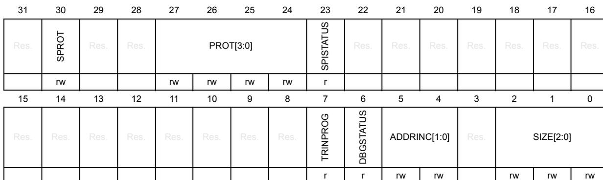
| 31 | 30 | 29 | 28 | 27 | 26 | 25 | 24 | 23 | 22 | 21 | 20 | 19 | 18 | 17 | 16 |
| Res. | SPROT | Res. | Res. | PROT[3:0] | SPSTATUS | Res. | Res. | Res. | Res. | Res. | Res. | Res. | |||
| rw | rw | rw | rw | rw | r | ||||||||||
| 15 | 14 | 13 | 12 | 11 | 10 | 9 | 8 | 7 | 6 | 5 | 4 | 3 | 2 | 1 | 0 |
| Res. | Res. | Res. | Res. | Res. | Res. | Res. | Res. | TRINPROG | DBGSTATUS | ADDRINC[1:0] | Res. | SIZE[2:0] | |||
| r | r | rw | rw | rw | rw | rw | |||||||||
Bit 31 Reserved, must be kept at reset value.
Bit 30 SPROT : secure transfer request
This field sets the protection attribute HPROT[6] of the bus transfer.0: reserved, must not be used
1: nonsecure transfer, HPROT[6] = high
Bits 29:28 Reserved, must be kept at reset value.
Bits 27:24 PROT[3:0] : bus transfer protection
This field sets the protection attributes HPROT[3:0] of the bus transfer.
bit 0 = 0: instruction access
bit 0 = 1: data access
bit 1 = 0: user mode
bit 1 = 1: privilege mode
bit 2 = 0: non-bufferable
bit 2 = 1: bufferable
bit 3 = 0: non-shareable, no look-up, non-modifiable
bit 3 = 1: shareable, look-up, modifiable
Bit 23 SPSTATUS : secure debug authentication status
This field indicates the state of the SPIDEN signal
0: No secure AHB transfers allowed
Bits 22:8 Reserved, must be kept at reset value.
Bit 7 TRINPROG : transfer in progress (read only)
This field indicates whether a transfer is currently in progress on the APB master port.
0: No AHB transfer in progress
1: AHB transfer in progress
Bit 6 DBGSTATUS : debug enable (DBGEN) status
0: AHB transfers blocked
1: AHB transfers enabled
Bits 5:4 ADDRINC[1:0] : auto-increment mode
This field defines whether the TAR address is automatically incremented after a transaction.
0x0: no auto-increment
0x1: address incremented by the size in bytes of the transaction (SIZE field). Single transfer.
0x2: address incremented by the size in bytes of the transaction (SIZE field). Packs four 8-bit transfers or two 16-bit transfers into a 32-bit DAP transfer. Multiple transactions are carried out on the AHB interface.
other: reserved, must not be used
Bit 3 Reserved, must be kept at reset value.
Bits 2:0 SIZE[2:0] : size of next memory access transaction
0x0: byte (8-bit)
0x1: halfword (16-bit)
0x2: word (32-bit)
others: reserved, must not be used
APx transfer address register (APx_TAR) (x = 0, 1)
Address offset: 0x04
Reset value: 0xXXXX XXXX
| 31 | 30 | 29 | 28 | 27 | 26 | 25 | 24 | 23 | 22 | 21 | 20 | 19 | 18 | 17 | 16 |
|---|---|---|---|---|---|---|---|---|---|---|---|---|---|---|---|
| TA[31:16] | |||||||||||||||
| rw | rw | rw | rw | rw | rw | rw | rw | rw | rw | rw | rw | rw | rw | rw | rw |
| 15 | 14 | 13 | 12 | 11 | 10 | 9 | 8 | 7 | 6 | 5 | 4 | 3 | 2 | 1 | 0 |
| TA[15:0] | |||||||||||||||
| rw | rw | rw | rw | rw | rw | rw | rw | rw | rw | rw | rw | rw | rw | rw | rw |
Bits 31:0 TA[31:0] : address of current transfer. In AP1, TA[1:0] are fixed at 0.
APx data read/write register (APx_DRW) (x = 0, 1)
Address offset: 0x0C
Reset value: 0xXXXX XXXX
| 31 | 30 | 29 | 28 | 27 | 26 | 25 | 24 | 23 | 22 | 21 | 20 | 19 | 18 | 17 | 16 |
|---|---|---|---|---|---|---|---|---|---|---|---|---|---|---|---|
| TD[31:16] | |||||||||||||||
| rw | rw | rw | rw | rw | rw | rw | rw | rw | rw | rw | rw | rw | rw | rw | rw |
| 15 | 14 | 13 | 12 | 11 | 10 | 9 | 8 | 7 | 6 | 5 | 4 | 3 | 2 | 1 | 0 |
| TD[15:0] | |||||||||||||||
| rw | rw | rw | rw | rw | rw | rw | rw | rw | rw | rw | rw | rw | rw | rw | rw |
Bits 31:0 TD[31:0] : data of current transfer
APx banked data n register (APx_BDn) (x = 0, 1)
Address offset: \( 0x10 + 0x4 * n \) , ( \( n = 0 \) to \( 3 \) )
Reset value: 0x0000 0000
| 31 | 30 | 29 | 28 | 27 | 26 | 25 | 24 | 23 | 22 | 21 | 20 | 19 | 18 | 17 | 16 |
| DATA[31:16] | |||||||||||||||
| rw | rw | rw | rw | rw | rw | rw | rw | rw | rw | rw | rw | rw | rw | rw | rw |
| 15 | 14 | 13 | 12 | 11 | 10 | 9 | 8 | 7 | 6 | 5 | 4 | 3 | 2 | 1 | 0 |
| DATA[15:0] | |||||||||||||||
| rw | rw | rw | rw | rw | rw | rw | rw | rw | rw | rw | rw | rw | rw | rw | rw |
Bits 31:0 DATA[31:0] : banked data of current transfer to address \( TA[31:4] + 4 * n \) .
Auto address incrementing is not performed on APx_BD0-3. Banked transfers are only supported for word transfers.
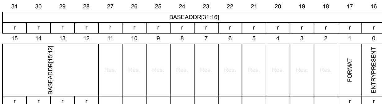
APx base address register (APx_BASE) (x = 0, 1)
Address offset: 0xF8
Reset value: AP 0: 0xF000 0003
Reset value: AP 1: 0xF000 0003
| 31 | 30 | 29 | 28 | 27 | 26 | 25 | 24 | 23 | 22 | 21 | 20 | 19 | 18 | 17 | 16 |
| BASEADDR[31:16] | |||||||||||||||
| r | r | r | r | r | r | r | r | r | r | r | r | r | r | r | r |
| 15 | 14 | 13 | 12 | 11 | 10 | 9 | 8 | 7 | 6 | 5 | 4 | 3 | 2 | 1 | 0 |
| BASEADDR[15:12] | Res. | Res. | Res. | Res. | Res. | Res. | Res. | Res. | Res. | Res. | FORMAT | ENTRYPRESENT | |||
| r | r | r | r | r | r | ||||||||||
Bits 31:12 BASEADDR[31:12] : base address (bits 31 to 12) of the first ROM table
The 12 LSBs are zero since the ROM table must be aligned on a 4-Kbyte boundary.
0xF0000: AP0
0xF0000: AP1
Bits 11:2 Reserved, must be kept at reset value.
Bit 1 FORMAT : base-address register format
1: Arm® debug interface v5
Bit 0 ENTRYPRESENT : debug components presence
This bit indicates that debug components are present on the access port bus.
1: debug components present
APx identification register (APx_IDR) (x = 0, 1)
Address offset: 0xFC
Reset value: AP 1: 0x5477 0002
Reset value: AP 0: 0x8477 0001
| 31 | 30 | 29 | 28 | 27 | 26 | 25 | 24 | 23 | 22 | 21 | 20 | 19 | 18 | 17 | 16 |
|---|---|---|---|---|---|---|---|---|---|---|---|---|---|---|---|
| REVISION[3:0] | JEDECBANK[3:0] | JEDECCODE[6:0] | CLASS[3] | ||||||||||||
| r | r | r | r | r | r | r | r | r | r | r | r | r | r | r | r |
| 15 | 14 | 13 | 12 | 11 | 10 | 9 | 8 | 7 | 6 | 5 | 4 | 3 | 2 | 1 | 0 |
| CLASS[2:0] | Res. | Res. | Res. | Res. | Res. | IDENTITY[7:0] | |||||||||
| r | r | r | r | r | r | r | r | r | r | r | |||||
Bits 31:28 REVISION[3:0] : revision number
0x5: r1p0
0x8: r0p9
Bits 27:24 JEDECBANK[3:0] : JEDEC bank
0x4: Arm ®
Bits 23:17 JEDECCODE[6:0] : JEDEC code
0x3B: Arm ®
Bits 16:13 CLASS[3:0] :
0x1: MEM-AP
Bits 12:8 Reserved, must be kept at reset value.
Bits 7:0 IDENTITY[7:0] :
0x1: AHB-AP
0x2: APB-AP
38.4.2 Access port register map
These registers are not on the CPU memory bus. They are only accessed through SW-DP debug interface.
The access port address is 8-bit wide, defined by DP_SELECT.APBANKSEL[3:0] field and by the SW-DP packet request A[3:2] field. The two least significant bits are 00.
Table 248. Access port register map and reset values
| Offset | Register name | 31 | 30 | 29 | 28 | 27 | 26 | 25 | 24 | 23 | 22 | 21 | 20 | 19 | 18 | 17 | 16 | 15 | 14 | 13 | 12 | 11 | 10 | 9 | 8 | 7 | 6 | 5 | 4 | 3 | 2 | 1 | 0 |
|---|---|---|---|---|---|---|---|---|---|---|---|---|---|---|---|---|---|---|---|---|---|---|---|---|---|---|---|---|---|---|---|---|---|
| DBGSWEN | Res. | Res. | Res. | Res. | Res. | Res. | Res. | Res. | Res. | Res. | Res. | Res. | Res. | Res. | Res. | Res. | Res. | Res. | Res. | MODE[3:0] | TRINPROG | DEVICEEN | ADDRINC[1:0] | Res. | SIZE[2:0] | ||||||||
| 0x00 | AP1_CSW | ||||||||||||||||||||||||||||||||
| Reset value | 1 | 0 | 0 | 0 | 0 | 0 | 1 | 0 | 0 | 0 | 1 | 0 | |||||||||||||||||||||
Table 248. Access port register map and reset values (continued)
| Offset | Register name | 31 | 30 | 29 | 28 | 27 | 26 | 25 | 24 | 23 | 22 | 21 | 20 | 19 | 18 | 17 | 16 | 15 | 14 | 13 | 12 | 11 | 10 | 9 | 8 | 7 | 6 | 5 | 4 | 3 | 2 | 1 | 0 | |
|---|---|---|---|---|---|---|---|---|---|---|---|---|---|---|---|---|---|---|---|---|---|---|---|---|---|---|---|---|---|---|---|---|---|---|
| 0x00 | AP0_CSW | Res. | SPROT | Res. | Res. | PROT[3:0] | SPISTATUS | Res. | Res. | Res. | Res. | Res. | Res. | Res. | Res. | Res. | Res. | Res. | MODE[3:0] | TRINPROG | DBGSTATUS | ADDRINC[1:0] | Res. | SIZE[2:0] | ||||||||||
| Reset value | 1 | 0 | 0 | 1 | 1 | X | 0 | 0 | 0 | 0 | 0 | X | 0 | 0 | 0 | 1 | 0 | |||||||||||||||||
| 0x04 | APx_TAR | TA[31:0] | ||||||||||||||||||||||||||||||||
| Reset value | X | X | X | X | X | X | X | X | X | X | X | X | X | X | X | X | X | X | X | X | X | X | X | X | X | X | X | X | X | X | X | X | ||
| 0x08 | Reserved | Reserved | ||||||||||||||||||||||||||||||||
| 0x0C | APx_DRW | TD[31:0] | ||||||||||||||||||||||||||||||||
| Reset value | X | X | X | X | X | X | X | X | X | X | X | X | X | X | X | X | X | X | X | X | X | X | X | X | X | X | X | X | X | X | X | X | ||
| 0x10 | APx_BD0 | DATA[31:0] | ||||||||||||||||||||||||||||||||
| Reset value | 0 | 0 | 0 | 0 | 0 | 0 | 0 | 0 | 0 | 0 | 0 | 0 | 0 | 0 | 0 | 0 | 0 | 0 | 0 | 0 | 0 | 0 | 0 | 0 | 0 | 0 | 0 | 0 | 0 | 0 | 0 | |||
| 0x14 | APx_BD1 | DATA[31:0] | ||||||||||||||||||||||||||||||||
| Reset value | 0 | 0 | 0 | 0 | 0 | 0 | 0 | 0 | 0 | 0 | 0 | 0 | 0 | 0 | 0 | 0 | 0 | 0 | 0 | 0 | 0 | 0 | 0 | 0 | 0 | 0 | 0 | 0 | 0 | 0 | 0 | |||
| 0x18 | APx_BD2 | DATA[31:0] | ||||||||||||||||||||||||||||||||
| Reset value | 0 | 0 | 0 | 0 | 0 | 0 | 0 | 0 | 0 | 0 | 0 | 0 | 0 | 0 | 0 | 0 | 0 | 0 | 0 | 0 | 0 | 0 | 0 | 0 | 0 | 0 | 0 | 0 | 0 | 0 | 0 | |||
| 0x1C | APx_BD3 | DATA[31:0] | ||||||||||||||||||||||||||||||||
| Reset value | 0 | 0 | 0 | 0 | 0 | 0 | 0 | 0 | 0 | 0 | 0 | 0 | 0 | 0 | 0 | 0 | 0 | 0 | 0 | 0 | 0 | 0 | 0 | 0 | 0 | 0 | 0 | 0 | 0 | 0 | 0 | |||
| 0x20 to 0xF4 | Reserved | Reserved | ||||||||||||||||||||||||||||||||
| 0xF8 | AP1_BASE | BASEADDR[31:12] | Res. | Res. | Res. | Res. | Res. | Res. | Res. | Res. | Res. | FORMAT | ENTRYPRESENT | |||||||||||||||||||||
| Reset value | 1 | 1 | 1 | 1 | 0 | 0 | 0 | 0 | 0 | 0 | 0 | 0 | 0 | 0 | 0 | 0 | 0 | 0 | 0 | 0 | 1 | 1 | ||||||||||||
| 0xF8 | AP0_BASE | BASEADDR[31:12] | Res. | Res. | Res. | Res. | Res. | Res. | Res. | Res. | Res. | FORMAT | ENTRYPRESENT | |||||||||||||||||||||
| Reset value | 1 | 1 | 1 | 1 | 0 | 0 | 0 | 0 | 0 | 0 | 0 | 0 | 0 | 0 | 0 | 0 | 0 | 0 | 0 | 0 | 1 | 1 | ||||||||||||
| 0xFC | AP1_IDR | REVISION[3:0] | JEDECBANK[3:0] | JEDECCODE[6:0] | CLASS[3:0] | Res. | Res. | Res. | Res. | Res. | IDENTITY[7:0] | |||||||||||||||||||||||
| Reset value | 0 | 1 | 0 | 1 | 0 | 1 | 0 | 0 | 0 | 1 | 1 | 1 | 0 | 1 | 1 | 1 | 0 | 0 | 0 | 0 | 0 | 0 | 0 | 0 | 0 | 0 | 1 | 0 | ||||||
| 0xFC | AP0_IDR | REVISION[3:0] | JEDECBANK[3:0] | JEDECCODE[6:0] | CLASS[3:0] | Res. | Res. | Res. | Res. | Res. | IDENTITY[7:0] | |||||||||||||||||||||||
| Reset value | 1 | 0 | 0 | 0 | 0 | 1 | 0 | 0 | 0 | 0 | 1 | 1 | 1 | 0 | 1 | 1 | 1 | 0 | 0 | 0 | 0 | 0 | 0 | 0 | 0 | 0 | 0 | 1 | ||||||
38.5 ROM tables
The ROM table is a CoreSight™ component that contains the base addresses of the CoreSight debug components accessible via the access port to which it is attached. These tables allow a debugger to discover the topology of the CoreSight system automatically.
There is one top level ROM table behind each access port, APn. The base address of this ROM table can be obtained by reading the APn_BASE register of the access port. The top level ROM table may point in turn to other ROM tables.
The system ROM table is pointed to by the AP1 base register, AP1_BASE. It contains the base address pointer for the DBGMCU.
The system ROM table occupies a 4-Kbyte, 32-bit wide chunk of the AP1 address space, from 0xF000 0000 to 0xF000 0FFC. It can be accessed by the debugger.
Table 249. System ROM table
| Address offset in ROM table | Component name | Component base address | Component address offset | Size (Kbytes) | Entry |
|---|---|---|---|---|---|
| 0x000 | DBGMCU | 0xF000 1000 (debugger) | 0x0000 1000 | 4 | 0x0000 1003 |
| 0x004 | Top of table | - | - | - | 0x0000 0000 |
| 0x008 to 0xFC8 | Reserved | - | - | - | 0x0000 0000 |
| 0xFCC to 0xFFC | ROM table registers | - | - | - | See Table 252 |
There are two ROM tables in the CPU subsystem. The MCU ROM table is pointed to by the AP0 base register, AP0_BASE. It contains the base-address pointer for the processor ROM table.
The MCU ROM table (see the table below) occupies a 4-Kbyte, 32-bit wide chunk of the AP0 address space, from 0xF000 0000 to 0xF000 0FFC. It is not accessible by software.
Table 250. MCU ROM table
| Address offset in ROM table | Component name | Component base address | Component address offset | Size (Kbytes) | Entry |
|---|---|---|---|---|---|
| 0x000 | Processor ROM table | 0xE00F F000 | 0x0000 1000 | 4 | 0xF00F F003 |
| 0x004 | Reserved | - | - | - | 0x0020 0002 |
| 0x008 | Reserved | - | - | - | 0x1000 0002 |
| 0x00C | Reserved | - | - | - | 0x1000 0002 |
| 0x010 | Top of table | - | - | - | 0x0000 0000 |
| 0x014 to 0xFC8 | Reserved | - | - | - | 0x0000 0000 |
| 0xFCC to 0xFFC | ROM table registers | - | - | - | See Table 253 |
The processor ROM table contains the base-address pointer for the system control space (SCS) registers that allow the debugger to identify the CPU core, as well as for the BPU, DWT.
The processor ROM table (see the table below) occupies a 4-Kbyte, 32-bit wide chunk of AP0 address space, from 0xE00F F000 to 0xE00F FFFC. It is not accessible by software.
Table 251. Processor ROM table
| Address in ROM table | Component name | Component base address | Component address offset | Size (Kbytes) | Entry |
|---|---|---|---|---|---|
| 0xE00F F000 | SCS | 0xE000 E000 | 0xFFF0 F000 | 4 | 0xFFF0 F003 |
| 0xE00F F004 | DWT | 0xE000 1000 | 0xFFF0 2000 | 4 | 0xFFF0 2003 |
| 0xE00F F008 | BPU | 0xE000 2000 | 0xFFF0 3000 | 4 | 0xFFF0 3003 |
| 0xE00F F00C | Top of table | - | - | - | 0x0000 0000 |
| 0xE00F F010 to 0xE00F FFC8 | Reserved | - | - | - | 0x0000 0000 |
| 0xE00F FFCC to 0xE00F FFFC | ROM table registers | - | - | - | See Table 254 |
The topology for the CoreSight components is shown in Figure 387 .
Figure 387. CoreSight topology
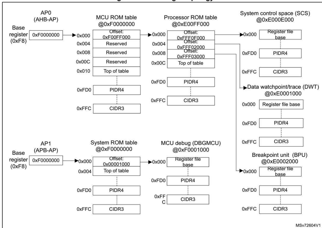
The diagram illustrates the CoreSight topology for two Access Port (AP) units: AP0 (AHB-AP) and AP1 (APB-AP). Each AP has a base register at address 0xF8.
- AP0 (AHB-AP):
- Base register (0xF8) points to address 0xF0000000.
- At 0xF0000000, the MCU ROM table is located. It contains entries for:
- Offset 0x000: 0xF00FF000 (points to the Processor ROM table at 0xE00FF000).
- Offset 0x004: Reserved.
- Offset 0x008: Reserved.
- Offset 0x00C: Reserved.
- Offset 0x010: Top of table.
- At 0xF0FD0, PIDR4 is located.
- At 0xF0FFC, CIDR3 is located.
- AP1 (APB-AP):
- Base register (0xF8) points to address 0xF0000000.
- At 0xF0000000, the System ROM table is located. It contains entries for:
- Offset 0x000: 0x00001000 (points to the MCU debug (DBGMCU) at 0xF0001000).
- Offset 0x004: Top of table.
- At 0xF0FD0, PIDR4 is located.
- At 0xF0FFC, CIDR3 is located.
- Processor ROM table (at 0xE00FF000):
- Offset 0x000: 0xFFF0F000 (points to the System control space (SCS) at 0xE000E000).
- Offset 0x004: 0xFFF02000 (points to the Data watchpoint/trace (DWT) at 0xE0001000).
- Offset 0x008: 0xFFF03000 (points to the Breakpoint unit (BPU) at 0xE0002000).
- Offset 0x00C: Top of table.
- MCU debug (DBGMCU) (at 0xF0001000):
- Offset 0x000: Register file base.
- Offset 0xFD0: PIDR4.
- Offset 0xFFC: CIDR3.
- System control space (SCS) (at 0xE000E000):
- Offset 0x000: Register file base.
- Offset 0xFD0: PIDR4.
- Offset 0xFFC: CIDR3.
- Data watchpoint/trace (DWT) (at 0xE0001000):
- Offset 0x000: Register file base.
- Offset 0xFD0: PIDR4.
- Offset 0xFFC: CIDR3.
- Breakpoint unit (BPU) (at 0xE0002000):
- Offset 0x000: Register file base.
- Offset 0xFD0: PIDR4.
- Offset 0xFFC: CIDR3.
MSV72604V1
38.5.1 System ROM table registers
System ROM memory type register (SYSROM_MEMTYPER)
Address offset: 0xFCC
Reset value: 0x0000 0001
| 31 | 30 | 29 | 28 | 27 | 26 | 25 | 24 | 23 | 22 | 21 | 20 | 19 | 18 | 17 | 16 |
|---|---|---|---|---|---|---|---|---|---|---|---|---|---|---|---|
| Res. | Res. | Res. | Res. | Res. | Res. | Res. | Res. | Res. | Res. | Res. | Res. | Res. | Res. | Res. | Res. |
| 15 | 14 | 13 | 12 | 11 | 10 | 9 | 8 | 7 | 6 | 5 | 4 | 3 | 2 | 1 | 0 |
| Res. | Res. | Res. | Res. | Res. | Res. | Res. | Res. | Res. | Res. | Res. | Res. | Res. | Res. | Res. | SYSTEM r |
Bits 31:1 Reserved, must be kept at reset value.
Bit 0 SYSTEM : system memory
0x1: system memory present on this bus
System ROM CoreSight peripheral identity register 4 (SYSROM_PIDR4)
Address offset: 0xFD0
Reset value: 0x0000 0000
| 31 | 30 | 29 | 28 | 27 | 26 | 25 | 24 | 23 | 22 | 21 | 20 | 19 | 18 | 17 | 16 |
|---|---|---|---|---|---|---|---|---|---|---|---|---|---|---|---|
| Res. | Res. | Res. | Res. | Res. | Res. | Res. | Res. | Res. | Res. | Res. | Res. | Res. | Res. | Res. | Res. |
| 15 | 14 | 13 | 12 | 11 | 10 | 9 | 8 | 7 | 6 | 5 | 4 | 3 | 2 | 1 | 0 |
| Res. | Res. | Res. | Res. | Res. | Res. | Res. | Res. | SIZE[3:0] | JEP106CON[3:0] | ||||||
| r | r | r | r | r | r | r | r | ||||||||
Bits 31:8 Reserved, must be kept at reset value.
Bits 7:4 SIZE[3:0] : register file size
0x0: The register file occupies a single 4-Kbyte region.
Bits 3:0 JEP106CON[3:0] : JEP106 continuation code
0x0: STMicroelectronics JEDEC continuation code
System ROM CoreSight peripheral identity register 0 (SYSROM_PIDR0)
Address offset: 0xFE0
Reset value: 0x0000 0000
| 31 | 30 | 29 | 28 | 27 | 26 | 25 | 24 | 23 | 22 | 21 | 20 | 19 | 18 | 17 | 16 |
|---|---|---|---|---|---|---|---|---|---|---|---|---|---|---|---|
| Res. | Res. | Res. | Res. | Res. | Res. | Res. | Res. | Res. | Res. | Res. | Res. | Res. | Res. | Res. | Res. |
| 15 | 14 | 13 | 12 | 11 | 10 | 9 | 8 | 7 | 6 | 5 | 4 | 3 | 2 | 1 | 0 |
| Res. | Res. | Res. | Res. | Res. | Res. | Res. | Res. | PARTNUM[7:0] | |||||||
| r | r | r | r | r | r | r | r | ||||||||
Bits 31:8 Reserved, must be kept at reset value.
Bits 7:0 PARTNUM[7:0] : part number bits [7:0]
0x00: STM32U0 series
System ROM CoreSight peripheral identity register 1 (SYSROM_PIDR1)
Address offset: 0xFE4
Reset value: 0x0000 0000
| 31 | 30 | 29 | 28 | 27 | 26 | 25 | 24 | 23 | 22 | 21 | 20 | 19 | 18 | 17 | 16 |
|---|---|---|---|---|---|---|---|---|---|---|---|---|---|---|---|
| Res. | Res. | Res. | Res. | Res. | Res. | Res. | Res. | Res. | Res. | Res. | Res. | Res. | Res. | Res. | Res. |
| 15 | 14 | 13 | 12 | 11 | 10 | 9 | 8 | 7 | 6 | 5 | 4 | 3 | 2 | 1 | 0 |
| Res. | Res. | Res. | Res. | Res. | Res. | Res. | Res. | JEP106ID[3:0] | PARTNUM[11:8] | ||||||
| r | r | r | r | r | r | r | r | ||||||||
Bits 31:8 Reserved, must be kept at reset value.
Bits 7:4 JEP106ID[3:0] : JEP106 identity code bits [3:0]
0x0: STMicroelectronics JEDEC code
Bits 3:0 PARTNUM[11:8] : part number bits [11:8]
0x0: STM32U0 series
System ROM CoreSight peripheral identity register 2 (SYSROM_PIDR2)
Address offset: 0xFE8
Reset value: 0x0000 000A
| 31 | 30 | 29 | 28 | 27 | 26 | 25 | 24 | 23 | 22 | 21 | 20 | 19 | 18 | 17 | 16 |
|---|---|---|---|---|---|---|---|---|---|---|---|---|---|---|---|
| Res. | Res. | Res. | Res. | Res. | Res. | Res. | Res. | Res. | Res. | Res. | Res. | Res. | Res. | Res. | Res. |
| 15 | 14 | 13 | 12 | 11 | 10 | 9 | 8 | 7 | 6 | 5 | 4 | 3 | 2 | 1 | 0 |
| Res. | Res. | Res. | Res. | Res. | Res. | Res. | Res. | REVISION[3:0] | JEDEC | JEP106ID[6:4] | |||||
| r | r | r | r | r | r | r | r | ||||||||
Bits 31:8 Reserved, must be kept at reset value.
Bits 7:4 REVISION[3:0] : component revision number
0x0: rev r0p0
Bit 3 JEDEC : JEDEC assigned value
1: designer identification specified by JEDEC
Bits 2:0 JEP106ID[6:4] : JEP106 identity code bits [6:4]
0x2: STMicroelectronics JEDEC code
System ROM CoreSight peripheral identity register 3 (SYSROM_PIDR3)
Address offset: 0xFEC
Reset value: 0x0000 0000
| 31 | 30 | 29 | 28 | 27 | 26 | 25 | 24 | 23 | 22 | 21 | 20 | 19 | 18 | 17 | 16 |
|---|---|---|---|---|---|---|---|---|---|---|---|---|---|---|---|
| Res. | Res. | Res. | Res. | Res. | Res. | Res. | Res. | Res. | Res. | Res. | Res. | Res. | Res. | Res. | Res. |
| 15 | 14 | 13 | 12 | 11 | 10 | 9 | 8 | 7 | 6 | 5 | 4 | 3 | 2 | 1 | 0 |
| Res. | Res. | Res. | Res. | Res. | Res. | Res. | Res. | REVAND[3:0] | CMOD[3:0] | ||||||
| r | r | r | r | r | r | r | r | ||||||||
Bits 31:8 Reserved, must be kept at reset value.
Bits 7:4 REVAND[3:0] : metal fix version
0x0: No metal fix
Bits 3:0 CMOD[3:0] : customer modified
0x0: No customer modifications
System ROM CoreSight component identity register 0 (SYSROM_CIDR0)
Address offset: 0xFF0
Reset value: 0x0000 000D
| 31 | 30 | 29 | 28 | 27 | 26 | 25 | 24 | 23 | 22 | 21 | 20 | 19 | 18 | 17 | 16 |
|---|---|---|---|---|---|---|---|---|---|---|---|---|---|---|---|
| Res. | Res. | Res. | Res. | Res. | Res. | Res. | Res. | Res. | Res. | Res. | Res. | Res. | Res. | Res. | Res. |
| 15 | 14 | 13 | 12 | 11 | 10 | 9 | 8 | 7 | 6 | 5 | 4 | 3 | 2 | 1 | 0 |
| Res. | Res. | Res. | Res. | Res. | Res. | Res. | Res. | PREAMBLE[7:0] | |||||||
| r | r | r | r | r | r | r | r | ||||||||
Bits 31:8 Reserved, must be kept at reset value.
Bits 7:0 PREAMBLE[7:0] : component identification bits [7:0]
0x0D: Common identification value
System ROM CoreSight peripheral identity register 1 (SYSROM_CIDR1)
Address offset: 0xFF4
Reset value: 0x0000 0010
| 31 | 30 | 29 | 28 | 27 | 26 | 25 | 24 | 23 | 22 | 21 | 20 | 19 | 18 | 17 | 16 |
|---|---|---|---|---|---|---|---|---|---|---|---|---|---|---|---|
| Res. | Res. | Res. | Res. | Res. | Res. | Res. | Res. | Res. | Res. | Res. | Res. | Res. | Res. | Res. | Res. |
| 15 | 14 | 13 | 12 | 11 | 10 | 9 | 8 | 7 | 6 | 5 | 4 | 3 | 2 | 1 | 0 |
| Res. | Res. | Res. | Res. | Res. | Res. | Res. | Res. | CLASS[3:0] | PREAMBLE[11:8] | ||||||
| r | r | r | r | r | r | r | r | ||||||||
Bits 31:8 Reserved, must be kept at reset value.
Bits 7:4 CLASS[3:0] : Component identification bits [15:12] - component class
0x1: ROM table component
Bits 3:0 PREAMBLE[11:8] : Component identification bits [11:8]
0x0: Common identification value
System ROM CoreSight component identity register 2 (SYSROM_CIDR2)
Address offset: 0xFF8
Reset value: 0x0000 0005
| 31 | 30 | 29 | 28 | 27 | 26 | 25 | 24 | 23 | 22 | 21 | 20 | 19 | 18 | 17 | 16 |
|---|---|---|---|---|---|---|---|---|---|---|---|---|---|---|---|
| Res. | Res. | Res. | Res. | Res. | Res. | Res. | Res. | Res. | Res. | Res. | Res. | Res. | Res. | Res. | Res. |
| 15 | 14 | 13 | 12 | 11 | 10 | 9 | 8 | 7 | 6 | 5 | 4 | 3 | 2 | 1 | 0 |
| Res. | Res. | Res. | Res. | Res. | Res. | Res. | Res. | PREAMBLE[19:12] | |||||||
| r | r | r | r | r | r | r | r | ||||||||
Bits 31:8 Reserved, must be kept at reset value.
Bits 7:0 PREAMBLE[19:12] : component identification bits [23:16]
0x05: common identification value
System ROM CoreSight component identity register 3 (SYSROM_CIDR3)
Address offset: 0xFFC
Reset value: 0x0000 00B1
| 31 | 30 | 29 | 28 | 27 | 26 | 25 | 24 | 23 | 22 | 21 | 20 | 19 | 18 | 17 | 16 |
|---|---|---|---|---|---|---|---|---|---|---|---|---|---|---|---|
| Res. | Res. | Res. | Res. | Res. | Res. | Res. | Res. | Res. | Res. | Res. | Res. | Res. | Res. | Res. | Res. |
| 15 | 14 | 13 | 12 | 11 | 10 | 9 | 8 | 7 | 6 | 5 | 4 | 3 | 2 | 1 | 0 |
| Res. | Res. | Res. | Res. | Res. | Res. | Res. | Res. | PREAMBLE[27:20] | |||||||
| r | r | r | r | r | r | r | r | ||||||||
Bits 31:8 Reserved, must be kept at reset value.
Bits 7:0 PREAMBLE[27:20] : Component identification bits [31:24]
0xB1: Common identification value
38.5.2 System ROM table register map
Table 252. System ROM table register map and reset values
| Offset | Register name | 31 | 30 | 29 | 28 | 27 | 26 | 25 | 24 | 23 | 22 | 21 | 20 | 19 | 18 | 17 | 16 | 15 | 14 | 13 | 12 | 11 | 10 | 9 | 8 | 7 | 6 | 5 | 4 | 3 | 2 | 1 | 0 | |
|---|---|---|---|---|---|---|---|---|---|---|---|---|---|---|---|---|---|---|---|---|---|---|---|---|---|---|---|---|---|---|---|---|---|---|
| 0xFCC | SYSROM_MEMTYPER | Res. | Res. | Res. | Res. | Res. | Res. | Res. | Res. | Res. | Res. | Res. | Res. | Res. | Res. | Res. | Res. | Res. | Res. | Res. | Res. | Res. | Res. | Res. | Res. | Res. | Res. | Res. | Res. | Res. | Res. | Res. | Res. | SYSTEMEM |
| Reset value | 1 | |||||||||||||||||||||||||||||||||
| 0xFD0 | SYSROM_PIDR4 | Res. | Res. | Res. | Res. | Res. | Res. | Res. | Res. | Res. | Res. | Res. | Res. | Res. | Res. | Res. | Res. | Res. | Res. | Res. | Res. | Res. | Res. | Res. | Res. | Res. | SIZE [3:0] | Res. | Res. | Res. | Res. | Res. | JEP106CON [3:0] | |
| Reset value | 0 | 0 | 0 | 0 | 0 | 0 | 0 | |||||||||||||||||||||||||||
| 0xFD4 to FDC | Reserved | Reserved | ||||||||||||||||||||||||||||||||
| 0xFE0 | SYSROM_PIDR0 | Res. | Res. | Res. | Res. | Res. | Res. | Res. | Res. | Res. | Res. | Res. | Res. | Res. | Res. | Res. | Res. | Res. | Res. | Res. | Res. | Res. | Res. | Res. | Res. | Res. | Res. | Res. | Res. | Res. | Res. | Res. | PARTNUM[7:0] | |
| Reset value | 0 | |||||||||||||||||||||||||||||||||
| 0xFE4 | SYSROM_PIDR1 | Res. | Res. | Res. | Res. | Res. | Res. | Res. | Res. | Res. | Res. | Res. | Res. | Res. | Res. | Res. | Res. | Res. | Res. | Res. | Res. | Res. | Res. | Res. | Res. | Res. | Res. | Res. | Res. | Res. | Res. | Res. | JEP106ID [3:0] PARTNUM [11:8] | |
| Reset value | 0 | |||||||||||||||||||||||||||||||||
| 0xFE8 | SYSROM_PIDR2 | Res. | Res. | Res. | Res. | Res. | Res. | Res. | Res. | Res. | Res. | Res. | Res. | Res. | Res. | Res. | Res. | Res. | Res. | Res. | Res. | Res. | Res. | Res. | Res. | Res. | Res. | Res. | Res. | Res. | Res. | Res. | REVISION [3:0] JEDEC JEP106ID [6:4] | |
| Reset value | 0 | |||||||||||||||||||||||||||||||||
| 0xFEC | SYSROM_PIDR3 | Res. | Res. | Res. | Res. | Res. | Res. | Res. | Res. | Res. | Res. | Res. | Res. | Res. | Res. | Res. | Res. | Res. | Res. | Res. | Res. | Res. | Res. | Res. | Res. | Res. | Res. | Res. | Res. | Res. | Res. | Res. | REVAND[3:0] CMOD[3:0] | |
| Reset value | 0 | |||||||||||||||||||||||||||||||||
| 0xFF0 | SYSROM_CIDR0 | Res. | Res. | Res. | Res. | Res. | Res. | Res. | Res. | Res. | Res. | Res. | Res. | Res. | Res. | Res. | Res. | Res. | Res. | Res. | Res. | Res. | Res. | Res. | Res. | Res. | Res. | Res. | Res. | Res. | Res. | Res. | PREAMBLE[7:0] | |
| Reset value | 0 | |||||||||||||||||||||||||||||||||
| 0xFF4 | SYSROM_CIDR1 | Res. | Res. | Res. | Res. | Res. | Res. | Res. | Res. | Res. | Res. | Res. | Res. | Res. | Res. | Res. | Res. | Res. | Res. | Res. | Res. | Res. | Res. | Res. | Res. | Res. | Res. | Res. | Res. | Res. | Res. | Res. | CLASS[3:0] PREAMBLE [11:8] | |
| Reset value | 0 | |||||||||||||||||||||||||||||||||
| 0xFF8 | SYSROM_CIDR2 | Res. | Res. | Res. | Res. | Res. | Res. | Res. | Res. | Res. | Res. | Res. | Res. | Res. | Res. | Res. | Res. | Res. | Res. | Res. | Res. | Res. | Res. | Res. | Res. | Res. | Res. | Res. | Res. | Res. | Res. | Res. | PREAMBLE[19:12] | |
| Reset value | 0 | |||||||||||||||||||||||||||||||||
| 0xFFC | SYSROM_CIDR3 | Res. | Res. | Res. | Res. | Res. | Res. | Res. | Res. | Res. | Res. | Res. | Res. | Res. | Res. | Res. | Res. | Res. | Res. | Res. | Res. | Res. | Res. | Res. | Res. | Res. | Res. | Res. | Res. | Res. | Res. | Res. | PREAMBLE[27:20] | |
| Reset value | 1 | |||||||||||||||||||||||||||||||||
Refer to Table 249: System ROM table for register boundary addresses.
38.5.3 MCU ROM table registers
MCU ROM memory type register (MCUROM_MEMTYPER)
Address offset: 0xFCC
Reset value: 0x0000 0001
| 31 | 30 | 29 | 28 | 27 | 26 | 25 | 24 | 23 | 22 | 21 | 20 | 19 | 18 | 17 | 16 |
|---|---|---|---|---|---|---|---|---|---|---|---|---|---|---|---|
| Res. | Res. | Res. | Res. | Res. | Res. | Res. | Res. | Res. | Res. | Res. | Res. | Res. | Res. | Res. | Res. |
| 15 | 14 | 13 | 12 | 11 | 10 | 9 | 8 | 7 | 6 | 5 | 4 | 3 | 2 | 1 | 0 |
| Res. | Res. | Res. | Res. | Res. | Res. | Res. | Res. | Res. | Res. | Res. | Res. | Res. | Res. | Res. | SYSTEM r |
Bits 31:1 Reserved, must be kept at reset value.
Bit 0 SYSTEM : system memory
0x1: system memory present on this bus
MCU ROM CoreSight peripheral identity register 4 (MCUROM_PIDR4)
Address offset: 0xFD0
Reset value: 0x0000 0000
| 31 | 30 | 29 | 28 | 27 | 26 | 25 | 24 | 23 | 22 | 21 | 20 | 19 | 18 | 17 | 16 |
|---|---|---|---|---|---|---|---|---|---|---|---|---|---|---|---|
| Res. | Res. | Res. | Res. | Res. | Res. | Res. | Res. | Res. | Res. | Res. | Res. | Res. | Res. | Res. | Res. |
| 15 | 14 | 13 | 12 | 11 | 10 | 9 | 8 | 7 | 6 | 5 | 4 | 3 | 2 | 1 | 0 |
| Res. | Res. | Res. | Res. | Res. | Res. | Res. | Res. | SIZE[3:0] | JEP106CON[3:0] | ||||||
| r | r | r | r | r | r | r | r |
Bits 31:8 Reserved, must be kept at reset value.
Bits 7:4 SIZE[3:0] : register file size
0x0: The register file occupies a single 4-Kbyte region.
Bits 3:0 JEP106CON[3:0] : JEP106 continuation code
0x0: STMicroelectronics JEDEC continuation code
MCU ROM CoreSight peripheral identity register 0 (MCUROM_PIDR0)
Address offset: 0xFE0
Reset value: 0x0000 0089
| 31 | 30 | 29 | 28 | 27 | 26 | 25 | 24 | 23 | 22 | 21 | 20 | 19 | 18 | 17 | 16 |
|---|---|---|---|---|---|---|---|---|---|---|---|---|---|---|---|
| Res. | Res. | Res. | Res. | Res. | Res. | Res. | Res. | Res. | Res. | Res. | Res. | Res. | Res. | Res. | Res. |
| 15 | 14 | 13 | 12 | 11 | 10 | 9 | 8 | 7 | 6 | 5 | 4 | 3 | 2 | 1 | 0 |
| Res. | Res. | Res. | Res. | Res. | Res. | Res. | Res. | PARTNUM[7:0] | |||||||
| r | r | r | r | r | r | r | r | ||||||||
Bits 31:8 Reserved, must be kept at reset value.
Bits 7:0 PARTNUM[7:0] : part number bits [7:0]
0x89: STM32U0 series
MCU ROM CoreSight peripheral identity register 1(MCUROM_PIDR1)
Address offset: 0xFE4
Reset value: 0x0000 0004
| 31 | 30 | 29 | 28 | 27 | 26 | 25 | 24 | 23 | 22 | 21 | 20 | 19 | 18 | 17 | 16 |
|---|---|---|---|---|---|---|---|---|---|---|---|---|---|---|---|
| Res. | Res. | Res. | Res. | Res. | Res. | Res. | Res. | Res. | Res. | Res. | Res. | Res. | Res. | Res. | Res. |
| 15 | 14 | 13 | 12 | 11 | 10 | 9 | 8 | 7 | 6 | 5 | 4 | 3 | 2 | 1 | 0 |
| Res. | Res. | Res. | Res. | Res. | Res. | Res. | Res. | JEP106ID[3:0] | PARTNUM[11:8] | ||||||
| r | r | r | r | r | r | r | r | ||||||||
Bits 31:8 Reserved, must be kept at reset value.
Bits 7:4 JEP106ID[3:0] : JEP106 identity code bits [3:0]
0x0: STMicroelectronics JEDEC code
Bits 3:0 PARTNUM[11:8] : part number bits [11:8]
0x4: STM32U0 series
MCU ROM CoreSight peripheral identity register 2 (MCUROM_PIDR2)
Address offset: 0xFE8
Reset value: 0x0000 000A
| 31 | 30 | 29 | 28 | 27 | 26 | 25 | 24 | 23 | 22 | 21 | 20 | 19 | 18 | 17 | 16 |
|---|---|---|---|---|---|---|---|---|---|---|---|---|---|---|---|
| Res. | Res. | Res. | Res. | Res. | Res. | Res. | Res. | Res. | Res. | Res. | Res. | Res. | Res. | Res. | Res. |
| 15 | 14 | 13 | 12 | 11 | 10 | 9 | 8 | 7 | 6 | 5 | 4 | 3 | 2 | 1 | 0 |
| Res. | Res. | Res. | Res. | Res. | Res. | Res. | Res. | REVISION[3:0] | JEDEC | JEP106ID[6:4] | |||||
| r | r | r | r | r | r | r | r | ||||||||
Bits 31:8 Reserved, must be kept at reset value.
Bits 7:4
REVISION[3:0]
: component revision number
0x0: rev r0p0
Bit 3
JEDEC
: JEDEC assigned value
1: designer identification specified by JEDEC
Bits 2:0
JEP106ID[6:4]
: JEP106 identity code bits [6:4]
0x2: STMicroelectronics JEDEC code
MCU ROM CoreSight peripheral identity register 3 (MCUROM_PIDR3)
Address offset: 0xFEC
Reset value: 0x0000 0000
| 31 | 30 | 29 | 28 | 27 | 26 | 25 | 24 | 23 | 22 | 21 | 20 | 19 | 18 | 17 | 16 |
|---|---|---|---|---|---|---|---|---|---|---|---|---|---|---|---|
| Res. | Res. | Res. | Res. | Res. | Res. | Res. | Res. | Res. | Res. | Res. | Res. | Res. | Res. | Res. | Res. |
| 15 | 14 | 13 | 12 | 11 | 10 | 9 | 8 | 7 | 6 | 5 | 4 | 3 | 2 | 1 | 0 |
| Res. | Res. | Res. | Res. | Res. | Res. | Res. | Res. | REVAND[3:0] | CMOD[3:0] | ||||||
| r | r | r | r | r | r | r | r | ||||||||
Bits 31:8 Reserved, must be kept at reset value.
Bits 7:4
REVAND[3:0]
: metal fix version
0x0: No metal fix
Bits 3:0
CMOD[3:0]
: customer modified
0x0: No customer modifications
MCU ROM CoreSight component identity register 0 (MCUROM_CIDR0)
Address offset: 0xFF0
Reset value: 0x0000 000D
| 31 | 30 | 29 | 28 | 27 | 26 | 25 | 24 | 23 | 22 | 21 | 20 | 19 | 18 | 17 | 16 |
|---|---|---|---|---|---|---|---|---|---|---|---|---|---|---|---|
| Res. | Res. | Res. | Res. | Res. | Res. | Res. | Res. | Res. | Res. | Res. | Res. | Res. | Res. | Res. | Res. |
| 15 | 14 | 13 | 12 | 11 | 10 | 9 | 8 | 7 | 6 | 5 | 4 | 3 | 2 | 1 | 0 |
| Res. | Res. | Res. | Res. | Res. | Res. | Res. | Res. | PREAMBLE[7:0] | |||||||
| r | r | r | r | r | r | r | r | ||||||||
Bits 31:8 Reserved, must be kept at reset value.
Bits 7:0
PREAMBLE[7:0]
: component identification bits [7:0]
0x0D: Common identification value
MCU ROM CoreSight peripheral identity register 1 (MCUROM_CIDR1)
Address offset: 0xFF4
Reset value: 0x0000 0010
| 31 | 30 | 29 | 28 | 27 | 26 | 25 | 24 | 23 | 22 | 21 | 20 | 19 | 18 | 17 | 16 |
|---|---|---|---|---|---|---|---|---|---|---|---|---|---|---|---|
| Res. | Res. | Res. | Res. | Res. | Res. | Res. | Res. | Res. | Res. | Res. | Res. | Res. | Res. | Res. | Res. |
| 15 | 14 | 13 | 12 | 11 | 10 | 9 | 8 | 7 | 6 | 5 | 4 | 3 | 2 | 1 | 0 |
| Res. | Res. | Res. | Res. | Res. | Res. | Res. | Res. | ||||||||
| CLASS[3:0] | PREAMBLE[11:8] | ||||||||||||||
| r | r | r | r | r | r | r | r | ||||||||
Bits 31:8 Reserved, must be kept at reset value.
Bits 7:4
CLASS[3:0]
: Component identification bits [15:12] - component class
0x1: ROM table component
Bits 3:0
PREAMBLE[11:8]
: Component identification bits [11:8]
0x0: Common identification value
MCU ROM CoreSight component identity register 2 (MCUROM_CIDR2)
Address offset: 0xFF8
Reset value: 0x0000 0005
| 31 | 30 | 29 | 28 | 27 | 26 | 25 | 24 | 23 | 22 | 21 | 20 | 19 | 18 | 17 | 16 |
|---|---|---|---|---|---|---|---|---|---|---|---|---|---|---|---|
| Res. | Res. | Res. | Res. | Res. | Res. | Res. | Res. | Res. | Res. | Res. | Res. | Res. | Res. | Res. | Res. |
| 15 | 14 | 13 | 12 | 11 | 10 | 9 | 8 | 7 | 6 | 5 | 4 | 3 | 2 | 1 | 0 |
| Res. | Res. | Res. | Res. | Res. | Res. | Res. | Res. | ||||||||
| PREAMBLE[19:12] | |||||||||||||||
| r | r | r | r | r | r | r | r | ||||||||
Bits 31:8 Reserved, must be kept at reset value.
Bits 7:0
PREAMBLE[19:12]
: component identification bits [23:16]
0x05: common identification value
MCU ROM CoreSight component identity register 3 (MCUROM_CIDR3)
Address offset: 0xFFC
Reset value: 0x0000 00B1
| 31 | 30 | 29 | 28 | 27 | 26 | 25 | 24 | 23 | 22 | 21 | 20 | 19 | 18 | 17 | 16 |
|---|---|---|---|---|---|---|---|---|---|---|---|---|---|---|---|
| Res. | Res. | Res. | Res. | Res. | Res. | Res. | Res. | Res. | Res. | Res. | Res. | Res. | Res. | Res. | Res. |
| 15 | 14 | 13 | 12 | 11 | 10 | 9 | 8 | 7 | 6 | 5 | 4 | 3 | 2 | 1 | 0 |
| Res. | Res. | Res. | Res. | Res. | Res. | Res. | Res. | ||||||||
| PREAMBLE[27:20] | |||||||||||||||
| r | r | r | r | r | r | r | r | ||||||||
Bits 31:8 Reserved, must be kept at reset value.
Bits 7:0 PREAMBLE[27:20] : Component identification bits [31:24]
0xB1: Common identification value
38.5.4 MCU ROM table register map
Table 253. MCU ROM table register map and reset values
| Offset | Register name | 31 | 30 | 29 | 28 | 27 | 26 | 25 | 24 | 23 | 22 | 21 | 20 | 19 | 18 | 17 | 16 | 15 | 14 | 13 | 12 | 11 | 10 | 9 | 8 | 7 | 6 | 5 | 4 | 3 | 2 | 1 | 0 |
|---|---|---|---|---|---|---|---|---|---|---|---|---|---|---|---|---|---|---|---|---|---|---|---|---|---|---|---|---|---|---|---|---|---|
| 0xFCC | MCUROM_MEMTYPER | Res. | Res. | Res. | Res. | Res. | Res. | Res. | Res. | Res. | Res. | Res. | Res. | Res. | Res. | Res. | Res. | Res. | Res. | Res. | Res. | Res. | Res. | Res. | Res. | Res. | Res. | Res. | Res. | Res. | Res. | Res. | SYSTEM |
| Reset value | 1 | ||||||||||||||||||||||||||||||||
| 0xFD0 | MCUROM_PIDR4 | Res. | Res. | Res. | Res. | Res. | Res. | Res. | Res. | Res. | Res. | Res. | Res. | Res. | Res. | Res. | Res. | Res. | Res. | Res. | Res. | Res. | Res. | Res. | Res. | SIZE [3:0] | JEP106CON [3:0] | ||||||
| Reset value | 0 | 0 | 0 | 0 | 0 | 0 | 0 | ||||||||||||||||||||||||||
| 0xFD4 to 0xFDC | Reserved | Reserved | |||||||||||||||||||||||||||||||
| 0xFE0 | MCUROM_PIDR0 | Res. | Res. | Res. | Res. | Res. | Res. | Res. | Res. | Res. | Res. | Res. | Res. | Res. | Res. | Res. | Res. | Res. | Res. | Res. | Res. | Res. | Res. | Res. | PARTNUM[7:0] | ||||||||
| Reset value | 1 | 0 | 0 | 0 | 1 | 1 | 0 | 0 | 1 | ||||||||||||||||||||||||
| 0xFE4 | MCUROM_PIDR1 | Res. | Res. | Res. | Res. | Res. | Res. | Res. | Res. | Res. | Res. | Res. | Res. | Res. | Res. | Res. | Res. | Res. | Res. | Res. | Res. | Res. | Res. | Res. | JEP106ID [3:0] | PARTNUM [11:8] | |||||||
| Reset value | 0 | 0 | 0 | 0 | 0 | 1 | 1 | 0 | 0 | ||||||||||||||||||||||||
| 0xFE8 | MCUROM_PIDR2 | Res. | Res. | Res. | Res. | Res. | Res. | Res. | Res. | Res. | Res. | Res. | Res. | Res. | Res. | Res. | Res. | Res. | Res. | Res. | Res. | Res. | Res. | Res. | REVISION [3:0] | JEDEC | JEP106ID [6:4] | ||||||
| Reset value | 0 | 0 | 0 | 0 | 0 | 1 | 0 | 1 | 0 | ||||||||||||||||||||||||
| 0xFEC | MCUROM_PIDR3 | Res. | Res. | Res. | Res. | Res. | Res. | Res. | Res. | Res. | Res. | Res. | Res. | Res. | Res. | Res. | Res. | Res. | Res. | Res. | Res. | Res. | Res. | Res. | REVAND[3:0] | CMOD[3:0] | |||||||
| Reset value | 0 | 0 | 0 | 0 | 0 | 0 | 0 | 0 | 0 | ||||||||||||||||||||||||
| 0xFF0 | MCUROM_CIDR0 | Res. | Res. | Res. | Res. | Res. | Res. | Res. | Res. | Res. | Res. | Res. | Res. | Res. | Res. | Res. | Res. | Res. | Res. | Res. | Res. | Res. | Res. | Res. | PREAMBLE[7:0] | ||||||||
| Reset value | 0 | 0 | 0 | 0 | 1 | 1 | 1 | 0 | 1 | ||||||||||||||||||||||||
| 0xFF4 | MCUROM_CIDR1 | Res. | Res. | Res. | Res. | Res. | Res. | Res. | Res. | Res. | Res. | Res. | Res. | Res. | Res. | Res. | Res. | Res. | Res. | Res. | Res. | Res. | Res. | Res. | CLASS[3:0] | PREAMBLE [11:8] | |||||||
| Reset value | 0 | 0 | 0 | 1 | 0 | 0 | 0 | 0 | 0 | ||||||||||||||||||||||||
| 0xFF8 | MCUROM_CIDR2 | Res. | Res. | Res. | Res. | Res. | Res. | Res. | Res. | Res. | Res. | Res. | Res. | Res. | Res. | Res. | Res. | Res. | Res. | Res. | Res. | Res. | Res. | Res. | PREAMBLE[19:12] | ||||||||
| Reset value | 0 | 0 | 0 | 0 | 0 | 1 | 1 | 0 | 1 | ||||||||||||||||||||||||
| 0xFFC | MCUROM_CIDR3 | Res. | Res. | Res. | Res. | Res. | Res. | Res. | Res. | Res. | Res. | Res. | Res. | Res. | Res. | Res. | Res. | Res. | Res. | Res. | Res. | Res. | Res. | Res. | PREAMBLE[27:20] | ||||||||
| Reset value | 1 | 0 | 1 | 1 | 0 | 0 | 0 | 0 | 1 | ||||||||||||||||||||||||
Refer to Table 250: MCU ROM table for register boundary addresses.
38.5.5 Processor ROM table registers
CPU ROM memory type register (CPUROM_MEMTYPER)
Address offset: 0xFCC
Reset value: 0x0000 0001
| 31 | 30 | 29 | 28 | 27 | 26 | 25 | 24 | 23 | 22 | 21 | 20 | 19 | 18 | 17 | 16 |
|---|---|---|---|---|---|---|---|---|---|---|---|---|---|---|---|
| Res. | Res. | Res. | Res. | Res. | Res. | Res. | Res. | Res. | Res. | Res. | Res. | Res. | Res. | Res. | Res. |
| 15 | 14 | 13 | 12 | 11 | 10 | 9 | 8 | 7 | 6 | 5 | 4 | 3 | 2 | 1 | 0 |
| Res. | Res. | Res. | Res. | Res. | Res. | Res. | Res. | Res. | Res. | Res. | Res. | Res. | Res. | Res. | SYSTEM r |
Bits 31:1 Reserved, must be kept at reset value.
Bit 0 SYSTEM : system memory
1: system memory present on this bus
CPU ROM CoreSight peripheral identity register 4 (CPUROM_PIDR4)
Address offset: 0xFD0
Reset value: 0x0000 0004
| 31 | 30 | 29 | 28 | 27 | 26 | 25 | 24 | 23 | 22 | 21 | 20 | 19 | 18 | 17 | 16 |
|---|---|---|---|---|---|---|---|---|---|---|---|---|---|---|---|
| Res. | Res. | Res. | Res. | Res. | Res. | Res. | Res. | Res. | Res. | Res. | Res. | Res. | Res. | Res. | Res. |
| 15 | 14 | 13 | 12 | 11 | 10 | 9 | 8 | 7 | 6 | 5 | 4 | 3 | 2 | 1 | 0 |
| Res. | Res. | Res. | Res. | Res. | Res. | Res. | Res. | r | r | r | r | r | r | r | r |
Bits 31:8 Reserved, must be kept at reset value.
Bits 7:4 SIZE[3:0] : register file size
0x0: The register file occupies a single 4-Kbyte region.
Bits 3:0 JEP106CON[3:0] : JEP106 continuation code
0x4: ARM JEDEC continuation code
CPU ROM CoreSight peripheral identity register 0 (CPUROM_PIDR0)
Address offset: 0xFE0
Reset value: 0x0000 00C0
| 31 | 30 | 29 | 28 | 27 | 26 | 25 | 24 | 23 | 22 | 21 | 20 | 19 | 18 | 17 | 16 |
|---|---|---|---|---|---|---|---|---|---|---|---|---|---|---|---|
| Res. | Res. | Res. | Res. | Res. | Res. | Res. | Res. | Res. | Res. | Res. | Res. | Res. | Res. | Res. | Res. |
| 15 | 14 | 13 | 12 | 11 | 10 | 9 | 8 | 7 | 6 | 5 | 4 | 3 | 2 | 1 | 0 |
| Res. | Res. | Res. | Res. | Res. | Res. | Res. | Res. | PARTNUM[7:0] | |||||||
| r | r | r | r | r | r | r | r | ||||||||
Bits 31:8 Reserved, must be kept at reset value.
Bits 7:0 PARTNUM[7:0] : Part number bits [7:0]
0xC0: Cortex ® -M0+
CPU ROM CoreSight peripheral identity register 1 (CPUROM_PIDR1)
Address offset: 0xFE4
Reset value: 0x0000 00B4
| 31 | 30 | 29 | 28 | 27 | 26 | 25 | 24 | 23 | 22 | 21 | 20 | 19 | 18 | 17 | 16 |
|---|---|---|---|---|---|---|---|---|---|---|---|---|---|---|---|
| Res. | Res. | Res. | Res. | Res. | Res. | Res. | Res. | Res. | Res. | Res. | Res. | Res. | Res. | Res. | Res. |
| 15 | 14 | 13 | 12 | 11 | 10 | 9 | 8 | 7 | 6 | 5 | 4 | 3 | 2 | 1 | 0 |
| Res. | Res. | Res. | Res. | Res. | Res. | Res. | Res. | JEP106ID[3:0] | PARTNUM[11:8] | ||||||
| r | r | r | r | r | r | r | r | ||||||||
Bits 31:8 Reserved, must be kept at reset value.
Bits 7:4 JEP106ID[3:0] : JEP106 identity code bits [3:0]
0xB: ARM ® JEDEC code
Bits 3:0 PARTNUM[11:8] : part number bits [11:8]
0x4: Cortex ® -M0+
CPU ROM CoreSight peripheral identity register 2 (CPUROM_PIDR2)
Address offset: 0xFE8
Reset value: 0x0000 000B
| 31 | 30 | 29 | 28 | 27 | 26 | 25 | 24 | 23 | 22 | 21 | 20 | 19 | 18 | 17 | 16 |
|---|---|---|---|---|---|---|---|---|---|---|---|---|---|---|---|
| Res. | Res. | Res. | Res. | Res. | Res. | Res. | Res. | Res. | Res. | Res. | Res. | Res. | Res. | Res. | Res. |
| 15 | 14 | 13 | 12 | 11 | 10 | 9 | 8 | 7 | 6 | 5 | 4 | 3 | 2 | 1 | 0 |
| Res. | Res. | Res. | Res. | Res. | Res. | Res. | Res. | REVISION[3:0] | JEDEC | JEP106ID[6:4] | |||||
| r | r | r | r | r | r | r | r | ||||||||
Bits 31:8 Reserved, must be kept at reset value.
Bits 7:4
REVISION[3:0]
: component revision number
0x0: rev r0p0
Bit 3
JEDEC
: JEDEC assigned value
1: Designer ID specified by JEDEC
Bits 2:0
JEP106ID[6:4]
: JEP106 identity code bits [6:4]
0x3: Arm® JEDEC code
CPU ROM CoreSight peripheral identity register 3 (CPUROM_PIDR3)
Address offset: 0xFEC
Reset value: 0x0000 0000
| 31 | 30 | 29 | 28 | 27 | 26 | 25 | 24 | 23 | 22 | 21 | 20 | 19 | 18 | 17 | 16 |
|---|---|---|---|---|---|---|---|---|---|---|---|---|---|---|---|
| Res. | Res. | Res. | Res. | Res. | Res. | Res. | Res. | Res. | Res. | Res. | Res. | Res. | Res. | Res. | Res. |
| 15 | 14 | 13 | 12 | 11 | 10 | 9 | 8 | 7 | 6 | 5 | 4 | 3 | 2 | 1 | 0 |
| Res. | Res. | Res. | Res. | Res. | Res. | Res. | Res. | REVAND[3:0] | CMOD[3:0] | ||||||
| r | r | r | r | r | r | r | r | ||||||||
Bits 31:8 Reserved, must be kept at reset value.
Bits 7:4
REVAND[3:0]
: metal fix version
0x0: No metal fix
Bits 3:0
CMOD[3:0]
: customer modified
0x0: no customer modifications
CPU ROM CoreSight component identity register 0 (CPUROM_CIDR0)
Address offset: 0xFF0
Reset value: 0x0000 000D
| 31 | 30 | 29 | 28 | 27 | 26 | 25 | 24 | 23 | 22 | 21 | 20 | 19 | 18 | 17 | 16 |
|---|---|---|---|---|---|---|---|---|---|---|---|---|---|---|---|
| Res. | Res. | Res. | Res. | Res. | Res. | Res. | Res. | Res. | Res. | Res. | Res. | Res. | Res. | Res. | Res. |
| 15 | 14 | 13 | 12 | 11 | 10 | 9 | 8 | 7 | 6 | 5 | 4 | 3 | 2 | 1 | 0 |
| Res. | Res. | Res. | Res. | Res. | Res. | Res. | Res. | PREAMBLE[7:0] | |||||||
| r | r | r | r | r | r | r | r | ||||||||
Bits 31:8 Reserved, must be kept at reset value.
Bits 7:0
PREAMBLE[7:0]
: Component identification bits [7:0]
0x0D: Common identification value
CPU ROM CoreSight peripheral identity register 1 (CPUROM_CIDR1)
Address offset: 0xFF4
Reset value: 0x0000 0010
| 31 | 30 | 29 | 28 | 27 | 26 | 25 | 24 | 23 | 22 | 21 | 20 | 19 | 18 | 17 | 16 |
|---|---|---|---|---|---|---|---|---|---|---|---|---|---|---|---|
| Res. | Res. | Res. | Res. | Res. | Res. | Res. | Res. | Res. | Res. | Res. | Res. | Res. | Res. | Res. | Res. |
| 15 | 14 | 13 | 12 | 11 | 10 | 9 | 8 | 7 | 6 | 5 | 4 | 3 | 2 | 1 | 0 |
| Res. | Res. | Res. | Res. | Res. | Res. | Res. | Res. | CLASS[3:0] | PREAMBLE[11:8] | ||||||
| r | r | r | r | r | r | r | r | ||||||||
Bits 31:8 Reserved, must be kept at reset value.
Bits 7:4 CLASS[3:0] : Component identification bits [15:12] - component class
0x1: ROM table component
Bits 3:0 PREAMBLE[11:8] : Component identification bits [11:8]
0x0: Common identification value
CPU ROM CoreSight component identity register 2 (CPUROM_CIDR2)
Address offset: 0xFF8
Reset value: 0x0000 0005
| 31 | 30 | 29 | 28 | 27 | 26 | 25 | 24 | 23 | 22 | 21 | 20 | 19 | 18 | 17 | 16 |
|---|---|---|---|---|---|---|---|---|---|---|---|---|---|---|---|
| Res. | Res. | Res. | Res. | Res. | Res. | Res. | Res. | Res. | Res. | Res. | Res. | Res. | Res. | Res. | Res. |
| 15 | 14 | 13 | 12 | 11 | 10 | 9 | 8 | 7 | 6 | 5 | 4 | 3 | 2 | 1 | 0 |
| Res. | Res. | Res. | Res. | Res. | Res. | Res. | Res. | PREAMBLE[19:12] | |||||||
| r | r | r | r | r | r | r | r | ||||||||
Bits 31:8 Reserved, must be kept at reset value.
Bits 7:0 PREAMBLE[19:12] : component identification bits [23:16]
0x05: common identification value
CPU ROM CoreSight component identity register 3 (CPUROM_CIDR3)
Address offset: 0xFFC
Reset value: 0x0000 00B1
| 31 | 30 | 29 | 28 | 27 | 26 | 25 | 24 | 23 | 22 | 21 | 20 | 19 | 18 | 17 | 16 |
|---|---|---|---|---|---|---|---|---|---|---|---|---|---|---|---|
| Res. | Res. | Res. | Res. | Res. | Res. | Res. | Res. | Res. | Res. | Res. | Res. | Res. | Res. | Res. | Res. |
| 15 | 14 | 13 | 12 | 11 | 10 | 9 | 8 | 7 | 6 | 5 | 4 | 3 | 2 | 1 | 0 |
| Res. | Res. | Res. | Res. | Res. | Res. | Res. | Res. | PREAMBLE[27:20] | |||||||
| r | r | r | r | r | r | r | r | ||||||||
Bits 31:8 Reserved, must be kept at reset value.
Bits 7:0 PREAMBLE[27:20] : component identification bits [31:24]
0xB1: common identification value
38.5.6 Processor ROM table register map
Table 254. CPU ROM table register map and reset values
| Offset | Register name | 31 | 30 | 29 | 28 | 27 | 26 | 25 | 24 | 23 | 22 | 21 | 20 | 19 | 18 | 17 | 16 | 15 | 14 | 13 | 12 | 11 | 10 | 9 | 8 | 7 | 6 | 5 | 4 | 3 | 2 | 1 | 0 |
|---|---|---|---|---|---|---|---|---|---|---|---|---|---|---|---|---|---|---|---|---|---|---|---|---|---|---|---|---|---|---|---|---|---|
| 0xFCC | CPUROM_MEMTYPER | Res. | Res. | Res. | Res. | Res. | Res. | Res. | Res. | Res. | Res. | Res. | Res. | Res. | Res. | Res. | Res. | Res. | Res. | Res. | Res. | Res. | Res. | Res. | Res. | Res. | Res. | Res. | Res. | Res. | Res. | Res. | SYSTEM |
| Reset value | 1 | ||||||||||||||||||||||||||||||||
| 0xFD4 to FDC | Reserved | Reserved | |||||||||||||||||||||||||||||||
| 0xFD0 | CPUROM_PIDR4 | Res. | Res. | Res. | Res. | Res. | Res. | Res. | Res. | Res. | Res. | Res. | Res. | Res. | Res. | Res. | Res. | Res. | Res. | Res. | Res. | Res. | Res. | Res. | Res. | SIZE [3:0] | JEP106CON [3:0] | ||||||
| Reset value | 0 | 0 | 0 | 0 | 0 | 1 | 0 | 0 | |||||||||||||||||||||||||
| 0xFE0 | CPUROM_PIDR0 | Res. | Res. | Res. | Res. | Res. | Res. | Res. | Res. | Res. | Res. | Res. | Res. | Res. | Res. | Res. | Res. | Res. | Res. | Res. | Res. | Res. | Res. | Res. | Res. | PARTNUM[7:0] | |||||||
| Reset value | 1 | 1 | 0 | 0 | 0 | 0 | 0 | 0 | |||||||||||||||||||||||||
| 0xFE4 | CPUROM_PIDR1 | Res. | Res. | Res. | Res. | Res. | Res. | Res. | Res. | Res. | Res. | Res. | Res. | Res. | Res. | Res. | Res. | Res. | Res. | Res. | Res. | Res. | Res. | Res. | Res. | JEP106ID [3:0] | PARTNUM [11:8] | ||||||
| Reset value | 1 | 0 | 1 | 1 | 0 | 1 | 0 | 0 | |||||||||||||||||||||||||
| 0xFE8 | CPUROM_PIDR2 | Res. | Res. | Res. | Res. | Res. | Res. | Res. | Res. | Res. | Res. | Res. | Res. | Res. | Res. | Res. | Res. | Res. | Res. | Res. | Res. | Res. | Res. | Res. | Res. | REVISION [3:0] | JEDEC | JEP106ID [6:4] | |||||
| Reset value | 0 | 0 | 0 | 0 | 1 | 0 | 1 | 1 | |||||||||||||||||||||||||
| 0xFEC | CPUROM_PIDR3 | Res. | Res. | Res. | Res. | Res. | Res. | Res. | Res. | Res. | Res. | Res. | Res. | Res. | Res. | Res. | Res. | Res. | Res. | Res. | Res. | Res. | Res. | Res. | Res. | REVAND[3:0] | CMOD[3:0] | ||||||
| Reset value | 0 | 0 | 0 | 0 | 0 | 0 | 0 | 0 | |||||||||||||||||||||||||
| 0xFF0 | CPUROM_CIDR0 | Res. | Res. | Res. | Res. | Res. | Res. | Res. | Res. | Res. | Res. | Res. | Res. | Res. | Res. | Res. | Res. | Res. | Res. | Res. | Res. | Res. | Res. | Res. | Res. | PREAMBLE[7:0] | |||||||
| Reset value | 0 | 0 | 0 | 0 | 1 | 1 | 0 | 1 | |||||||||||||||||||||||||
| 0xFF4 | CPUROM_CIDR1 | Res. | Res. | Res. | Res. | Res. | Res. | Res. | Res. | Res. | Res. | Res. | Res. | Res. | Res. | Res. | Res. | Res. | Res. | Res. | Res. | Res. | Res. | Res. | Res. | CLASS[3:0] | PREAMBLE [11:8] | ||||||
| Reset value | 0 | 0 | 0 | 1 | 0 | 0 | 0 | 0 | |||||||||||||||||||||||||
| 0xFF8 | CPUROM_CIDR2 | Res. | Res. | Res. | Res. | Res. | Res. | Res. | Res. | Res. | Res. | Res. | Res. | Res. | Res. | Res. | Res. | Res. | Res. | Res. | Res. | Res. | Res. | Res. | Res. | PREAMBLE[19:12] | |||||||
| Reset value | 0 | 0 | 0 | 0 | 0 | 1 | 0 | 1 | |||||||||||||||||||||||||
| 0xFFC | CPUROM_CIDR3 | Res. | Res. | Res. | Res. | Res. | Res. | Res. | Res. | Res. | Res. | Res. | Res. | Res. | Res. | Res. | Res. | Res. | Res. | Res. | Res. | Res. | Res. | Res. | Res. | PREAMBLE[27:20] | |||||||
| Reset value | 1 | 0 | 1 | 1 | 0 | 0 | 0 | 1 | |||||||||||||||||||||||||
Refer to Table 251: Processor ROM table for register boundary addresses.
38.6 Data watchpoint and trace unit (DWT)
The DWT provides two comparators that can be used as one of the following, according to the DWT function register x (DWT_FUNCTIONx) :
- • data address matching and creation of a watchpoint event
- • instruction address matching and creation of a PC watchpoint event.
A DWT comparator compares the value held in its DWT comparator x register (DWT_COMPx) with one of the following:
- • a data address
- • an instruction address
For address matching, the comparator can use a mask, so it matches a range of addresses, up to 2GB. The bits to be masked are programmed in DWT comparator x register (DWT_MASKx) .
On a successful match, the comparator generates a watchpoint debug event. A watchpoint debug event causes the processor to halt execution and enter debug state.
The DWT also provides a PC sampling register, DWT program counter sample register (DWT_PCSR) which allows the debugger to sample the program counter for code profiling.
The DWT features can only be used if the DWT enable (DWTENA) bit is set in the SCS_DEMCR register.
For more details on how to use the DWT, refer to the Arm v6-M Architecture Reference Manual [4].
38.6.1 DWT registers
The DWT registers are accessible to the debugger via access port AP0. They are not accessible by software running on the CPU.
DWT control register (DWT_CTRL)
Address offset: 0x000
Reset value: 0x2000 0000
| 31 | 30 | 29 | 28 | 27 | 26 | 25 | 24 | 23 | 22 | 21 | 20 | 19 | 18 | 17 | 16 |
|---|---|---|---|---|---|---|---|---|---|---|---|---|---|---|---|
| NUMCOMP[3:0] | Res. | Res. | Res. | Res. | Res. | Res. | Res. | Res. | Res. | Res. | Res. | Res. | |||
| r | r | r | r | ||||||||||||
| 15 | 14 | 13 | 12 | 11 | 10 | 9 | 8 | 7 | 6 | 5 | 4 | 3 | 2 | 1 | 0 |
| Res. | Res. | Res. | Res. | Res. | Res. | Res. | Res. | Res. | Res. | Res. | Res. | Res. | Res. | Res. | Res. |
Bits 31:28 NUMCOMP[3:0] : number of comparators implemented
0x4: four comparators
Bits 27:0 Reserved, must be kept at reset value.
DWT program counter sample register (DWT_PCSR)
Address offset: 0x01C
Reset value: 0xXXXX XXXX
| 31 | 30 | 29 | 28 | 27 | 26 | 25 | 24 | 23 | 22 | 21 | 20 | 19 | 18 | 17 | 16 |
|---|---|---|---|---|---|---|---|---|---|---|---|---|---|---|---|
| EIASAMPLE[31:16] | |||||||||||||||
| r | r | r | r | r | r | r | r | r | r | r | r | r | r | r | r |
| 15 | 14 | 13 | 12 | 11 | 10 | 9 | 8 | 7 | 6 | 5 | 4 | 3 | 2 | 1 | 0 |
| EIASAMPLE[15:0] | |||||||||||||||
| r | r | r | r | r | r | r | r | r | r | r | r | r | r | r | r |
Bits 31:0
EIASAMPLE[31:0]
: executed instruction address sample value.
Samples the current value of the program counter.
DWT comparator x register (DWT_COMPx)
Address offset: 0x020 + 0x010 * x, (x = 0 to 1)
Reset value: 0xXXXX XXXX
| 31 | 30 | 29 | 28 | 27 | 26 | 25 | 24 | 23 | 22 | 21 | 20 | 19 | 18 | 17 | 16 |
|---|---|---|---|---|---|---|---|---|---|---|---|---|---|---|---|
| COMP[31:16] | |||||||||||||||
| rw | rw | rw | rw | rw | rw | rw | rw | rw | rw | rw | rw | rw | rw | rw | rw |
| 15 | 14 | 13 | 12 | 11 | 10 | 9 | 8 | 7 | 6 | 5 | 4 | 3 | 2 | 1 | 0 |
| COMP[15:0] | |||||||||||||||
| rw | rw | rw | rw | rw | rw | rw | rw | rw | rw | rw | rw | rw | rw | rw | rw |
Bits 31:0 COMP[31:0] : reference value for comparison
DWT comparator x register (DWT_MASKx)
Address offset: 0x024 + 0x010 * x, (x = 0 to 1)
Reset value: 0xXXXX XXXX
| 31 | 30 | 29 | 28 | 27 | 26 | 25 | 24 | 23 | 22 | 21 | 20 | 19 | 18 | 17 | 16 |
|---|---|---|---|---|---|---|---|---|---|---|---|---|---|---|---|
| Res. | Res. | Res. | Res. | Res. | Res. | Res. | Res. | Res. | Res. | Res. | Res. | Res. | Res. | Res. | Res. |
| 15 | 14 | 13 | 12 | 11 | 10 | 9 | 8 | 7 | 6 | 5 | 4 | 3 | 2 | 1 | 0 |
| Res. | Res. | Res. | Res. | Res. | Res. | Res. | Res. | Res. | Res. | Res. | MASK[4:0] | ||||
| rw | rw | rw | rw | rw | |||||||||||
Bits 31:5 Reserved, must be kept at reset value.
Bits 4:0
MASK[4:0]
: size of the ignore mask applied to address range matching
Writing all ones to this field and reading it back can be used to determine the maximum mask size supported.
Address offset: 0x028 + 0x010 * x, (x = 0 to 1)
Reset value: 0x5800 0000
| 31 | 30 | 29 | 28 | 27 | 26 | 25 | 24 | 23 | 22 | 21 | 20 | 19 | 18 | 17 | 16 |
|---|---|---|---|---|---|---|---|---|---|---|---|---|---|---|---|
| Res. | Res. | Res. | Res. | Res. | Res. | Res. | MATCHED | Res. | Res. | Res. | Res. | Res. | Res. | Res. | Res. |
| 15 | 14 | 13 | 12 | 11 | 10 | 9 | 8 | 7 | 6 | 5 | 4 | 3 | 2 | 1 | 0 |
| Res. | Res. | Res. | Res. | Res. | Res. | Res. | Res. | Res. | Res. | Res. | Res. | FUNCTION[3:0] | |||
| r | rw | rw | rw | rw | |||||||||||
Bits 31:25 Reserved, must be kept at reset value.
Bit 24 MATCHED : comparator matchThis bit indicates if a comparator match has occurred since the register was last read.
0: no match
1: a match occurred
Bits 23:4 Reserved, must be kept at reset value.
Bits 3:0 FUNCTION[3:0] : Action on comparator match0x0: Comparator disabled
0x4: PC watchpoint event on instruction address match
0x5: Watchpoint event on data read address match
0x6: Watchpoint event on data write address match
0x7: Watchpoint event on data read or write address match
others: reserved, must not be used
DWT CoreSight peripheral identity register 4 (DWT_PIDR4)Address offset: 0xFD0
Reset value: 0x0000 0004
| 31 | 30 | 29 | 28 | 27 | 26 | 25 | 24 | 23 | 22 | 21 | 20 | 19 | 18 | 17 | 16 |
|---|---|---|---|---|---|---|---|---|---|---|---|---|---|---|---|
| Res. | Res. | Res. | Res. | Res. | Res. | Res. | Res. | Res. | Res. | Res. | Res. | Res. | Res. | Res. | Res. |
| 15 | 14 | 13 | 12 | 11 | 10 | 9 | 8 | 7 | 6 | 5 | 4 | 3 | 2 | 1 | 0 |
| Res. | Res. | Res. | Res. | Res. | Res. | Res. | Res. | SIZE[3:0] | JEP106CON[3:0] | ||||||
| r | r | r | r | r | r | r | r | ||||||||
Bits 31:8 Reserved, must be kept at reset value.
Bits 7:4 SIZE[3:0] : register file size0x0: The register file occupies a single 4-Kbyte region.
Bits 3:0 JEP106CON[3:0] : JEP106 continuation code0x4: Arm® JEDEC code
DWT CoreSight peripheral identity register 0 (DWT_PIDR0)Address offset: 0xFE0
Reset value: 0x0000 000A
| 31 | 30 | 29 | 28 | 27 | 26 | 25 | 24 | 23 | 22 | 21 | 20 | 19 | 18 | 17 | 16 |
|---|---|---|---|---|---|---|---|---|---|---|---|---|---|---|---|
| Res. | Res. | Res. | Res. | Res. | Res. | Res. | Res. | Res. | Res. | Res. | Res. | Res. | Res. | Res. | Res. |
| 15 | 14 | 13 | 12 | 11 | 10 | 9 | 8 | 7 | 6 | 5 | 4 | 3 | 2 | 1 | 0 |
| Res. | Res. | Res. | Res. | Res. | Res. | Res. | Res. | PARTNUM[7:0] | |||||||
| r | r | r | r | r | r | r | r | ||||||||
Bits 31:8 Reserved, must be kept at reset value.
Bits 7:0 PARTNUM[7:0] : part number bits [7:0]0x0A: Cortex ® -M0+ DWT part number DWT CoreSight peripheral identity register 1 (DWT_PIDR1)Address offset: 0xFE4
Reset value: 0x0000 00B0
| 31 | 30 | 29 | 28 | 27 | 26 | 25 | 24 | 23 | 22 | 21 | 20 | 19 | 18 | 17 | 16 |
|---|---|---|---|---|---|---|---|---|---|---|---|---|---|---|---|
| Res. | Res. | Res. | Res. | Res. | Res. | Res. | Res. | Res. | Res. | Res. | Res. | Res. | Res. | Res. | Res. |
| 15 | 14 | 13 | 12 | 11 | 10 | 9 | 8 | 7 | 6 | 5 | 4 | 3 | 2 | 1 | 0 |
| Res. | Res. | Res. | Res. | Res. | Res. | Res. | Res. | JEP106ID[3:0] | PARTNUM[11:8] | ||||||
Bits 31:8 Reserved, must be kept at reset value.
Bits 7:4 JEP106ID[3:0] : JEP106 identity code bits [3:0]0xB: Arm ® JEDEC codeBits 3:0 PARTNUM[11:8] : part number bits [11:8]0x0: Cortex ® -M0+ DWT part number DWT CoreSight peripheral identity register 2 (DWT_PIDR2)Address offset: 0xFE8
Reset value: 0x0000 000B
| 31 | 30 | 29 | 28 | 27 | 26 | 25 | 24 | 23 | 22 | 21 | 20 | 19 | 18 | 17 | 16 |
|---|---|---|---|---|---|---|---|---|---|---|---|---|---|---|---|
| Res. | Res. | Res. | Res. | Res. | Res. | Res. | Res. | Res. | Res. | Res. | Res. | Res. | Res. | Res. | Res. |
| 15 | 14 | 13 | 12 | 11 | 10 | 9 | 8 | 7 | 6 | 5 | 4 | 3 | 2 | 1 | 0 |
| Res. | Res. | Res. | Res. | Res. | Res. | Res. | Res. | REVISION[3:0] | JEDEC | JEP106ID[6:4] | |||||
Bits 31:8 Reserved, must be kept at reset value.
Bits 7:4 REVISION[3:0] : component revision number
0x0: r0p0
Bit 3 JEDEC : JEDEC assigned value
0x1: designer identification specified by JEDEC
Bits 2:0 JEP106ID[6:4] : JEP106 identity code bits [6:4]
0x3: Arm® JEDEC code
DWT CoreSight peripheral identity register 3 (DWT_PIDR3)
Address offset: 0xFEC
Reset value: 0x0000 0000
| 31 | 30 | 29 | 28 | 27 | 26 | 25 | 24 | 23 | 22 | 21 | 20 | 19 | 18 | 17 | 16 |
|---|---|---|---|---|---|---|---|---|---|---|---|---|---|---|---|
| Res. | Res. | Res. | Res. | Res. | Res. | Res. | Res. | Res. | Res. | Res. | Res. | Res. | Res. | Res. | Res. |
| 15 | 14 | 13 | 12 | 11 | 10 | 9 | 8 | 7 | 6 | 5 | 4 | 3 | 2 | 1 | 0 |
| Res. | Res. | Res. | Res. | Res. | Res. | Res. | Res. | REVAND[3:0] | CMOD[3:0] | ||||||
| r | r | r | r | r | r | r | r | ||||||||
Bits 31:8 Reserved, must be kept at reset value.
Bits 7:4 REVAND[3:0] : metal fix version
0x0: no metal fix
Bits 3:0 CMOD[3:0] : customer modified
0x0: No customer modifications
DWT CoreSight component identity register 0 (DWT_CIDR0)
Address offset: 0xFF0
Reset value: 0x0000 000D
| 31 | 30 | 29 | 28 | 27 | 26 | 25 | 24 | 23 | 22 | 21 | 20 | 19 | 18 | 17 | 16 |
|---|---|---|---|---|---|---|---|---|---|---|---|---|---|---|---|
| Res. | Res. | Res. | Res. | Res. | Res. | Res. | Res. | Res. | Res. | Res. | Res. | Res. | Res. | Res. | Res. |
| 15 | 14 | 13 | 12 | 11 | 10 | 9 | 8 | 7 | 6 | 5 | 4 | 3 | 2 | 1 | 0 |
| Res. | Res. | Res. | Res. | Res. | Res. | Res. | Res. | PREAMBLE[7:0] | |||||||
| r | r | r | r | r | r | r | r | ||||||||
Bits 31:8 Reserved, must be kept at reset value.
Bits 7:0 PREAMBLE[7:0] : component identification bits [7:0]
0x0D: Common identification value
DWT CoreSight peripheral identity register 1 (DWT_CIDR1)
Address offset: 0xFF4
Reset value: 0x0000 00E0
| 31 | 30 | 29 | 28 | 27 | 26 | 25 | 24 | 23 | 22 | 21 | 20 | 19 | 18 | 17 | 16 |
|---|---|---|---|---|---|---|---|---|---|---|---|---|---|---|---|
| Res. | Res. | Res. | Res. | Res. | Res. | Res. | Res. | Res. | Res. | Res. | Res. | Res. | Res. | Res. | Res. |
| 15 | 14 | 13 | 12 | 11 | 10 | 9 | 8 | 7 | 6 | 5 | 4 | 3 | 2 | 1 | 0 |
| Res. | Res. | Res. | Res. | Res. | Res. | Res. | Res. | ||||||||
| CLASS[3:0] | PREAMBLE[11:8] | ||||||||||||||
| r | r | r | r | r | r | r | r | ||||||||
Bits 31:8 Reserved, must be kept at reset value.
Bits 7:4 CLASS[3:0] : component identification bits [15:12] - component class
0xE: Generic IP component
Bits 3:0 PREAMBLE[11:8] : component identification bits [11:8]
0x0: common identification value
DWT CoreSight component identity register 2 (DWT_CIDR2)
Address offset: 0xFF8
Reset value: 0x0000 0005
| 31 | 30 | 29 | 28 | 27 | 26 | 25 | 24 | 23 | 22 | 21 | 20 | 19 | 18 | 17 | 16 |
|---|---|---|---|---|---|---|---|---|---|---|---|---|---|---|---|
| Res. | Res. | Res. | Res. | Res. | Res. | Res. | Res. | Res. | Res. | Res. | Res. | Res. | Res. | Res. | Res. |
| 15 | 14 | 13 | 12 | 11 | 10 | 9 | 8 | 7 | 6 | 5 | 4 | 3 | 2 | 1 | 0 |
| Res. | Res. | Res. | Res. | Res. | Res. | Res. | Res. | ||||||||
| PREAMBLE[19:12] | |||||||||||||||
| r | r | r | r | r | r | r | r | ||||||||
Bits 31:8 Reserved, must be kept at reset value.
Bits 7:0 PREAMBLE[19:12] : component identification bits [23:16]
0x05: common identification value
DWT CoreSight component identity register 3 (DWT_CIDR3)
Address offset: 0xFFC
Reset value: 0x0000 00B1
| 31 | 30 | 29 | 28 | 27 | 26 | 25 | 24 | 23 | 22 | 21 | 20 | 19 | 18 | 17 | 16 |
|---|---|---|---|---|---|---|---|---|---|---|---|---|---|---|---|
| Res. | Res. | Res. | Res. | Res. | Res. | Res. | Res. | Res. | Res. | Res. | Res. | Res. | Res. | Res. | Res. |
| 15 | 14 | 13 | 12 | 11 | 10 | 9 | 8 | 7 | 6 | 5 | 4 | 3 | 2 | 1 | 0 |
| Res. | Res. | Res. | Res. | Res. | Res. | Res. | Res. | ||||||||
| PREAMBLE[27:20] | |||||||||||||||
| r | r | r | r | r | r | r | r | ||||||||
Bits 31:8 Reserved, must be kept at reset value.
Bits 7:0 PREAMBLE[27:20] : component identification bits [31:24]
0xB1: common identification value
38.6.2 DWT register map
Refer to Table 251: Processor ROM table for DWT register bank base address.
Table 255. DWT register map and reset values
| Offset | Register name | 31 | 30 | 29 | 28 | 27 | 26 | 25 | 24 | 23 | 22 | 21 | 20 | 19 | 18 | 17 | 16 | 15 | 14 | 13 | 12 | 11 | 10 | 9 | 8 | 7 | 6 | 5 | 4 | 3 | 2 | 1 | 0 |
|---|---|---|---|---|---|---|---|---|---|---|---|---|---|---|---|---|---|---|---|---|---|---|---|---|---|---|---|---|---|---|---|---|---|
| 0x000 | DWT_CTRL | NUMCOMP[3:0] | Res. | Res. | Res. | Res. | Res. | Res. | Res. | Res. | Res. | Res. | Res. | Res. | Res. | Res. | Res. | Res. | Res. | Res. | Res. | Res. | Res. | Res. | Res. | Res. | Res. | Res. | Res. | Res. | Res. | ||
| Reset value | 0 | 0 | 1 | 0 | |||||||||||||||||||||||||||||
| 0x004 to 0x018 | Reserved | Reserved | |||||||||||||||||||||||||||||||
| 0x01C | DWT_PCSR | EIASAMPLE[31:0] | |||||||||||||||||||||||||||||||
| Reset value | X | X | X | X | X | X | X | X | X | X | X | X | X | X | X | X | X | X | X | X | X | X | X | X | X | X | X | X | X | X | X | X | |
| 0x020 | DWT_COMP0 | COMP[31:0] | |||||||||||||||||||||||||||||||
| Reset value | X | X | X | X | X | X | X | X | X | X | X | X | X | X | X | X | X | X | X | X | X | X | X | X | X | X | X | X | X | X | X | X | |
| 0x024 | DWT_MASK0 | Res. | Res. | Res. | Res. | Res. | Res. | Res. | Res. | Res. | Res. | Res. | Res. | Res. | Res. | Res. | Res. | Res. | Res. | Res. | Res. | Res. | Res. | Res. | Res. | Res. | Res. | Res. | Res. | MASK[4:0] | |||
| Reset value | 0 | 0 | 0 | 0 | |||||||||||||||||||||||||||||
| 0x028 | DWT_FUNCTION0 | Res. | Res. | Res. | Res. | Res. | Res. | Res. | o | Res. | Res. | Res. | Res. | Res. | Res. | Res. | Res. | Res. | Res. | Res. | Res. | Res. | Res. | Res. | Res. | Res. | Res. | Res. | Res. | MATCH[3:0] | |||
| Reset value | o | 0 | 0 | 0 | 0 | ||||||||||||||||||||||||||||
| 0x02C | Reserved | Reserved | |||||||||||||||||||||||||||||||
| 0x030 | DWT_COMP1 | COMP[31:0] | |||||||||||||||||||||||||||||||
| Reset value | X | X | X | X | X | X | X | X | X | X | X | X | X | X | X | X | X | X | X | X | X | X | X | X | X | X | X | X | X | X | X | X | |
| 0x034 | DWT_MASK1 | Res. | Res. | Res. | Res. | Res. | Res. | Res. | Res. | Res. | Res. | Res. | Res. | Res. | Res. | Res. | Res. | Res. | Res. | Res. | Res. | Res. | Res. | Res. | Res. | Res. | Res. | Res. | Res. | MASK[4:0] | |||
| Reset value | 0 | 0 | 0 | 0 | |||||||||||||||||||||||||||||
| 0x038 | DWT_FUNCTION1 | Res. | Res. | Res. | Res. | Res. | Res. | Res. | o | Res. | Res. | Res. | Res. | Res. | Res. | Res. | Res. | Res. | Res. | Res. | Res. | Res. | Res. | Res. | Res. | Res. | Res. | Res. | Res. | MATCH[3:0] | |||
| Reset value | o | 0 | 0 | 0 | 0 | ||||||||||||||||||||||||||||
| 0x03C to 0xFCC | Reserved | Reserved | |||||||||||||||||||||||||||||||
| 0xFD0 | DWT_PIDR4 | Res. | Res. | Res. | Res. | Res. | Res. | Res. | Res. | Res. | Res. | Res. | Res. | Res. | Res. | Res. | Res. | Res. | Res. | Res. | Res. | Res. | Res. | Res. | Res. | Res. | Res. | SIZE[3:0] | JEP106CON[3:0] | ||||
| Reset value | 0 | 0 | 0 | 1 | |||||||||||||||||||||||||||||
| 0xFD4 to 0xFDC | Reserved | Reserved | |||||||||||||||||||||||||||||||
Table 255. DWT register map and reset values (continued)
| Offset | Register name | 31 | 30 | 29 | 28 | 27 | 26 | 25 | 24 | 23 | 22 | 21 | 20 | 19 | 18 | 17 | 16 | 15 | 14 | 13 | 12 | 11 | 10 | 9 | 8 | 7 | 6 | 5 | 4 | 3 | 2 | 1 | 0 |
|---|---|---|---|---|---|---|---|---|---|---|---|---|---|---|---|---|---|---|---|---|---|---|---|---|---|---|---|---|---|---|---|---|---|
| 0xFE0 | DWT_PIDR0 | Res. | Res. | Res. | Res. | Res. | Res. | Res. | Res. | Res. | Res. | Res. | Res. | Res. | Res. | Res. | Res. | Res. | Res. | Res. | Res. | Res. | Res. | Res. | PARTNUM[7:0] | ||||||||
| Reset value | 0 | 0 | 0 | 0 | 1 | 0 | 1 | 0 | |||||||||||||||||||||||||
| 0xFE4 | DWT_PIDR1 | Res. | Res. | Res. | Res. | Res. | Res. | Res. | Res. | Res. | Res. | Res. | Res. | Res. | Res. | Res. | Res. | Res. | Res. | Res. | Res. | Res. | Res. | JEP106ID[3:0] | PARTNUM[11:8] | ||||||||
| Reset value | |||||||||||||||||||||||||||||||||
| 0xFE8 | DWT_PIDR2 | Res. | Res. | Res. | Res. | Res. | Res. | Res. | Res. | Res. | Res. | Res. | Res. | Res. | Res. | Res. | Res. | Res. | Res. | Res. | Res. | Res. | Res. | REVISION[3:0] | JEDEC | ||||||||
| Reset value | |||||||||||||||||||||||||||||||||
| 0xFEC | DWT_PIDR3 | Res. | Res. | Res. | Res. | Res. | Res. | Res. | Res. | Res. | Res. | Res. | Res. | Res. | Res. | Res. | Res. | Res. | Res. | Res. | Res. | Res. | Res. | REVAND[3:0] | CMOD[3:0] | ||||||||
| Reset value | 0 | 0 | 0 | 0 | 0 | 0 | 0 | 0 | |||||||||||||||||||||||||
| 0xFF0 | DWT_CIDR0 | Res. | Res. | Res. | Res. | Res. | Res. | Res. | Res. | Res. | Res. | Res. | Res. | Res. | Res. | Res. | Res. | Res. | Res. | Res. | Res. | Res. | Res. | PREAMBLE[7:0] | |||||||||
| Reset value | 0 | 0 | 0 | 0 | 1 | 1 | 0 | 1 | |||||||||||||||||||||||||
| 0xFF4 | DWT_CIDR1 | Res. | Res. | Res. | Res. | Res. | Res. | Res. | Res. | Res. | Res. | Res. | Res. | Res. | Res. | Res. | Res. | Res. | Res. | Res. | Res. | Res. | Res. | CLASS[3:0] | PREAMBLE[11:8] | ||||||||
| Reset value | |||||||||||||||||||||||||||||||||
| 0xFF8 | DWT_CIDR2 | Res. | Res. | Res. | Res. | Res. | Res. | Res. | Res. | Res. | Res. | Res. | Res. | Res. | Res. | Res. | Res. | Res. | Res. | Res. | Res. | Res. | Res. | PREAMBLE[19:12] | |||||||||
| Reset value | 0 | 0 | 0 | 0 | 0 | 1 | 0 | 1 | |||||||||||||||||||||||||
| 0xFFC | DWT_CIDR3 | Res. | Res. | Res. | Res. | Res. | Res. | Res. | Res. | Res. | Res. | Res. | Res. | Res. | Res. | Res. | Res. | Res. | Res. | Res. | Res. | Res. | Res. | PREAMBLE[27:20] | |||||||||
| Reset value | 1 | 0 | 1 | 1 | 0 | 0 | 0 | 1 | |||||||||||||||||||||||||
38.7 Breakpoint unit (BPU)
The BPU allows the user to set hardware breakpoints. It contains four comparators that monitor the instruction fetch address. If a match occurs, the instruction comparators can be configured to generate a breakpoint event.
For more information on the breakpoint unit and how to use it, refer to [4].
38.7.1 BPU registers
The BPU registers are accessible to the debugger via access port AP0. They are not accessible by software running on the CPU.
BPU control register (BPU_CTRL)
Address offset: 0x000
Reset value: 0x0000 0040
| 31 | 30 | 29 | 28 | 27 | 26 | 25 | 24 | 23 | 22 | 21 | 20 | 19 | 18 | 17 | 16 |
|---|---|---|---|---|---|---|---|---|---|---|---|---|---|---|---|
| Res. | Res. | Res. | Res. | Res. | Res. | Res. | Res. | Res. | Res. | Res. | Res. | Res. | Res. | Res. | Res. |
| 15 | 14 | 13 | 12 | 11 | 10 | 9 | 8 | 7 | 6 | 5 | 4 | 3 | 2 | 1 | 0 |
| Res. | Res. | Res. | Res. | Res. | Res. | Res. | Res. | NUM_CODE[3:0] | Res. | Res. | KEY | ENABLE | |||
| r | r | r | r | rw | rw | ||||||||||
Bits 31:8 Reserved, must be kept at reset value.
Bits 7:4
NUM_CODE[3:0]
: number of instruction address comparators supported
0x04: 8 instruction comparators supported
Bits 3:2 Reserved, must be kept at reset value.
Bit 1 KEY : Write protect key.
This bit must be set when writing to BPU_CTRL register, otherwise the write is ignored.
Bit 0 ENABLE : BPU enable
- 0: disabled
- 1: enabled
BPU comparator x register (BPU_COMPx)
Address offset: 0x008 + 0x004 * x, (x = 0 to 3)
Reset value: 0xXXXX XXXX
| 31 | 30 | 29 | 28 | 27 | 26 | 25 | 24 | 23 | 22 | 21 | 20 | 19 | 18 | 17 | 16 |
|---|---|---|---|---|---|---|---|---|---|---|---|---|---|---|---|
| BP_MATCH[1:0] | Res. | COMP[28:16] | |||||||||||||
| rw | rw | rw | rw | rw | rw | rw | rw | rw | rw | rw | rw | rw | rw | rw | |
| 15 | 14 | 13 | 12 | 11 | 10 | 9 | 8 | 7 | 6 | 5 | 4 | 3 | 2 | 1 | 0 |
| COMP[15:2] | Res. | ENABLE | |||||||||||||
| rw | rw | rw | rw | rw | rw | rw | rw | rw | rw | rw | rw | rw | rw | rw | |
Bits 31:30 BP_MATCH[1:0] : behavior when COMP field is matched to the instruction fetch address and ENABLE = 1.
- 00: no breakpoint
- 01: breakpoint if lower half-word of address matches (16-bit and 32-bit instructions)
- 10: breakpoint if upper half-word of address matches (16-bit instructions only)
- 11: breakpoint if both lower and upper half-word of address match (16 and 32-bit instructions)
Bit 29 Reserved, must be kept at reset value.
Bits 28:2 COMP[28:2] : Bits 28:2 of the comparison address.
Bits 31:29 and 1:0 of the comparison address are fixed to 0. The comparison address is compared with the instruction address fetched from code memory.
Bit 1 Reserved, must be kept at reset value.
Bit 0 ENABLE : breakpoint enable
- 0: disabled
- 1: enabled
BPU CoreSight peripheral identity register 4 (BPU_PIDR4)
Address offset: 0xFD0
Reset value: 0x0000 0004
| 31 | 30 | 29 | 28 | 27 | 26 | 25 | 24 | 23 | 22 | 21 | 20 | 19 | 18 | 17 | 16 |
|---|---|---|---|---|---|---|---|---|---|---|---|---|---|---|---|
| Res. | Res. | Res. | Res. | Res. | Res. | Res. | Res. | Res. | Res. | Res. | Res. | Res. | Res. | Res. | Res. |
| 15 | 14 | 13 | 12 | 11 | 10 | 9 | 8 | 7 | 6 | 5 | 4 | 3 | 2 | 1 | 0 |
| Res. | Res. | Res. | Res. | Res. | Res. | Res. | Res. | SIZE[3:0] | JEP106CON[3:0] | ||||||
| r | r | r | r | r | r | r | r | ||||||||
Bits 31:8 Reserved, must be kept at reset value.
Bits 7:4 SIZE[3:0] : register file size
0x0: The register file occupies a single 4-Kbyte region.
Bits 3:0 JEP106CON[3:0] : JEP106 continuation code
0x4: Arm® JEDEC code
BPU CoreSight peripheral identity register 0 (BPU_PIDR0)
Address offset: 0xFE0
Reset value: 0x0000 000B
| 31 | 30 | 29 | 28 | 27 | 26 | 25 | 24 | 23 | 22 | 21 | 20 | 19 | 18 | 17 | 16 |
|---|---|---|---|---|---|---|---|---|---|---|---|---|---|---|---|
| Res. | Res. | Res. | Res. | Res. | Res. | Res. | Res. | Res. | Res. | Res. | Res. | Res. | Res. | Res. | Res. |
| 15 | 14 | 13 | 12 | 11 | 10 | 9 | 8 | 7 | 6 | 5 | 4 | 3 | 2 | 1 | 0 |
| Res. | Res. | Res. | Res. | Res. | Res. | Res. | Res. | PARTNUM[7:0] | |||||||
| r | r | r | r | r | r | r | r | ||||||||
Bits 31:8 Reserved, must be kept at reset value.
Bits 7:0
PARTNUM[7:0]
: part number bits [7:0]
0x0B: BPU part number
BPU CoreSight peripheral identity register 1 (BPU_PIDR1)
Address offset: 0xFE4
Reset value: 0x0000 00BD
| 31 | 30 | 29 | 28 | 27 | 26 | 25 | 24 | 23 | 22 | 21 | 20 | 19 | 18 | 17 | 16 |
|---|---|---|---|---|---|---|---|---|---|---|---|---|---|---|---|
| Res. | Res. | Res. | Res. | Res. | Res. | Res. | Res. | Res. | Res. | Res. | Res. | Res. | Res. | Res. | Res. |
| 15 | 14 | 13 | 12 | 11 | 10 | 9 | 8 | 7 | 6 | 5 | 4 | 3 | 2 | 1 | 0 |
| Res. | Res. | Res. | Res. | Res. | Res. | Res. | Res. | JEP106ID[3:0] | PARTNUM[11:8] | ||||||
| r | r | r | r | r | r | r | r | ||||||||
Bits 31:8 Reserved, must be kept at reset value.
Bits 7:4
JEP106ID[3:0]
: JEP106 identity code bits [3:0]
0xB: Arm
®
JEDEC code
Bits 3:0
PARTNUM[11:8]
: part number bits [11:8]
0x0: BPU part number
BPU CoreSight peripheral identity register 2 (BPU_PIDR2)
Address offset: 0xFE8
Reset value: 0x0000 000B
| 31 | 30 | 29 | 28 | 27 | 26 | 25 | 24 | 23 | 22 | 21 | 20 | 19 | 18 | 17 | 16 |
|---|---|---|---|---|---|---|---|---|---|---|---|---|---|---|---|
| Res. | Res. | Res. | Res. | Res. | Res. | Res. | Res. | Res. | Res. | Res. | Res. | Res. | Res. | Res. | Res. |
| 15 | 14 | 13 | 12 | 11 | 10 | 9 | 8 | 7 | 6 | 5 | 4 | 3 | 2 | 1 | 0 |
| Res. | Res. | Res. | Res. | Res. | Res. | Res. | Res. | REVISION[3:0] | JEDEC | JEP106ID[6:4] | |||||
| r | r | r | r | r | r | r | r | ||||||||
Bits 31:8 Reserved, must be kept at reset value.
Bits 7:4
REVISION[3:0]
: component revision number
0x0: r0p0
Bit 3
JEDEC
: JEDEC assigned value
0x1: designer identification specified by JEDEC
Bits 2:0
JEP106ID[6:4]
: JEP106 identity code bits [6:4]
0x3: Arm
®
JEDEC code
Address offset: 0xFEC
Reset value: 0x0000 0000
| 31 | 30 | 29 | 28 | 27 | 26 | 25 | 24 | 23 | 22 | 21 | 20 | 19 | 18 | 17 | 16 |
|---|---|---|---|---|---|---|---|---|---|---|---|---|---|---|---|
| Res. | Res. | Res. | Res. | Res. | Res. | Res. | Res. | Res. | Res. | Res. | Res. | Res. | Res. | Res. | Res. |
| 15 | 14 | 13 | 12 | 11 | 10 | 9 | 8 | 7 | 6 | 5 | 4 | 3 | 2 | 1 | 0 |
| Res. | Res. | Res. | Res. | Res. | Res. | Res. | Res. | REVAND[3:0] | CMOD[3:0] | ||||||
| r | r | r | r | r | r | r | r | ||||||||
Bits 31:8 Reserved, must be kept at reset value.
Bits 7:4 REVAND[3:0] : metal fix version0x0: no metal fix
Bits 3:0 CMOD[3:0] : customer modified0x0: no customer modifications
BPU CoreSight component identity register 0 (BPU_CIDR0)Address offset: 0xFF0
Reset value: 0x0000 000D
| 31 | 30 | 29 | 28 | 27 | 26 | 25 | 24 | 23 | 22 | 21 | 20 | 19 | 18 | 17 | 16 |
|---|---|---|---|---|---|---|---|---|---|---|---|---|---|---|---|
| Res. | Res. | Res. | Res. | Res. | Res. | Res. | Res. | Res. | Res. | Res. | Res. | Res. | Res. | Res. | Res. |
| 15 | 14 | 13 | 12 | 11 | 10 | 9 | 8 | 7 | 6 | 5 | 4 | 3 | 2 | 1 | 0 |
| Res. | Res. | Res. | Res. | Res. | Res. | Res. | Res. | PREAMBLE[7:0] | |||||||
| r | r | r | r | r | r | r | r | ||||||||
Bits 31:8 Reserved, must be kept at reset value.
Bits 7:0 PREAMBLE[7:0] : component identification bits [7:0]0x0D: common identification value
BPU CoreSight peripheral identity register 1 (BPU_CIDR1)Address offset: 0xFF4
Reset value: 0x0000 00E0
| 31 | 30 | 29 | 28 | 27 | 26 | 25 | 24 | 23 | 22 | 21 | 20 | 19 | 18 | 17 | 16 |
|---|---|---|---|---|---|---|---|---|---|---|---|---|---|---|---|
| Res. | Res. | Res. | Res. | Res. | Res. | Res. | Res. | Res. | Res. | Res. | Res. | Res. | Res. | Res. | Res. |
| 15 | 14 | 13 | 12 | 11 | 10 | 9 | 8 | 7 | 6 | 5 | 4 | 3 | 2 | 1 | 0 |
| Res. | Res. | Res. | Res. | Res. | Res. | Res. | Res. | CLASS[3:0] | PREAMBLE[11:8] | ||||||
| r | r | r | r | r | r | r | r | ||||||||
Bits 31:8 Reserved, must be kept at reset value.
Bits 7:4
CLASS[3:0]
: component identification bits [15:12] - component class
0xE: generic IP
Bits 3:0
PREAMBLE[11:8]
: component identification bits [11:8]
0x0: common identification value
BPU CoreSight component identity register 2 (BPU_CIDR2)
Address offset: 0xFF8
Reset value: 0x0000 0005
| 31 | 30 | 29 | 28 | 27 | 26 | 25 | 24 | 23 | 22 | 21 | 20 | 19 | 18 | 17 | 16 |
|---|---|---|---|---|---|---|---|---|---|---|---|---|---|---|---|
| Res. | Res. | Res. | Res. | Res. | Res. | Res. | Res. | Res. | Res. | Res. | Res. | Res. | Res. | Res. | Res. |
| 15 | 14 | 13 | 12 | 11 | 10 | 9 | 8 | 7 | 6 | 5 | 4 | 3 | 2 | 1 | 0 |
| Res. | Res. | Res. | Res. | Res. | Res. | Res. | Res. | PREAMBLE[19:12] | |||||||
| r | r | r | r | r | r | r | r | ||||||||
Bits 31:8 Reserved, must be kept at reset value.
Bits 7:0
PREAMBLE[19:12]
: component identification bits [23:16]
0x05: common identification value
BPU CoreSight component identity register 3 (BPU_CIDR3)
Address offset: 0xFFC
Reset value: 0x0000 00B1
| 31 | 30 | 29 | 28 | 27 | 26 | 25 | 24 | 23 | 22 | 21 | 20 | 19 | 18 | 17 | 16 |
|---|---|---|---|---|---|---|---|---|---|---|---|---|---|---|---|
| Res. | Res. | Res. | Res. | Res. | Res. | Res. | Res. | Res. | Res. | Res. | Res. | Res. | Res. | Res. | Res. |
| 15 | 14 | 13 | 12 | 11 | 10 | 9 | 8 | 7 | 6 | 5 | 4 | 3 | 2 | 1 | 0 |
| Res. | Res. | Res. | Res. | Res. | Res. | Res. | Res. | PREAMBLE[27:20] | |||||||
| r | r | r | r | r | r | r | r | ||||||||
Bits 31:8 Reserved, must be kept at reset value.
Bits 7:0
PREAMBLE[27:20]
: component identification bits [31:24]
0xB1: common identification value
38.7.2 BPU register map
Refer to Table 251: Processor ROM table for register boundary addresses.
Table 256. BPU register map and reset values
| Offset | Register name | 31 | 30 | 29 | 28 | 27 | 26 | 25 | 24 | 23 | 22 | 21 | 20 | 19 | 18 | 17 | 16 | 15 | 14 | 13 | 12 | 11 | 10 | 9 | 8 | 7 | 6 | 5 | 4 | 3 | 2 | 1 | 0 |
|---|---|---|---|---|---|---|---|---|---|---|---|---|---|---|---|---|---|---|---|---|---|---|---|---|---|---|---|---|---|---|---|---|---|
| 0x000 | BPU_CTRL | Res. | Res. | Res. | Res. | Res. | Res. | Res. | Res. | Res. | Res. | Res. | Res. | Res. | Res. | Res. | Res. | Res. | Res. | Res. | Res. | Res. | Res. | Res. | Res. | Res. | NUM_CODE [3:0] | Res. | Res. | Res. | Res. | KEY | ENABLE |
| Reset value | 1 | 0 | 0 | 0 | 0 | 0 | |||||||||||||||||||||||||||
| 0x004 | Reserved | Reserved | |||||||||||||||||||||||||||||||
| 0x008 to 0x014 | BPU_COMP0 to BPU_COMP3 | BP_MATCH[1:0] | Res. | COMP[28:2] | Res. | ENABLE | |||||||||||||||||||||||||||
| Reset value | X | X | X | X | X | X | X | X | X | X | X | X | X | X | X | X | X | X | X | X | X | X | X | X | X | X | X | X | X | 0 | |||
| 0x018 to 0xFCC | Reserved | Reserved | |||||||||||||||||||||||||||||||
| 0xFD0 | BPU_PIDR4 | Res. | Res. | Res. | Res. | Res. | Res. | Res. | Res. | Res. | Res. | Res. | Res. | Res. | Res. | Res. | Res. | Res. | Res. | Res. | Res. | Res. | Res. | Res. | Res. | Res. | SIZE [3:0] | JEP106CON [3:0] | |||||
| Reset value | |||||||||||||||||||||||||||||||||
| 0xFD4 to 0xFDC | Reserved | Reserved | |||||||||||||||||||||||||||||||
| 0xFE0 | BPU_PIDR0 | Res. | Res. | Res. | Res. | Res. | Res. | Res. | Res. | Res. | Res. | Res. | Res. | Res. | Res. | Res. | Res. | Res. | Res. | Res. | Res. | Res. | Res. | Res. | Res. | Res. | PARTNUM[7:0] | ||||||
| Reset value | 0 | 0 | 0 | 0 | 1 | 0 | |||||||||||||||||||||||||||
| 0xFE4 | BPU_PIDR1 | Res. | Res. | Res. | Res. | Res. | Res. | Res. | Res. | Res. | Res. | Res. | Res. | Res. | Res. | Res. | Res. | Res. | Res. | Res. | Res. | Res. | Res. | Res. | Res. | JEP106ID [3:0] | |||||||
| Reset value | |||||||||||||||||||||||||||||||||
| 0xFE8 | BPU_PIDR2 | Res. | Res. | Res. | Res. | Res. | Res. | Res. | Res. | Res. | Res. | Res. | Res. | Res. | Res. | Res. | Res. | Res. | Res. | Res. | Res. | Res. | Res. | Res. | Res. | REVISION [3:0] | JEDEC | ||||||
| Reset value | |||||||||||||||||||||||||||||||||
| 0xFEC | BPU_PIDR3 | Res. | Res. | Res. | Res. | Res. | Res. | Res. | Res. | Res. | Res. | Res. | Res. | Res. | Res. | Res. | Res. | Res. | Res. | Res. | Res. | Res. | Res. | Res. | Res. | REVAND[3:0] | |||||||
| Reset value | |||||||||||||||||||||||||||||||||
| 0xFF0 | BPU_CIDR0 | Res. | Res. | Res. | Res. | Res. | Res. | Res. | Res. | Res. | Res. | Res. | Res. | Res. | Res. | Res. | Res. | Res. | Res. | Res. | Res. | Res. | Res. | Res. | Res. | PREAMBLE[7:0] | |||||||
| Reset value | 0 | 0 | 0 | 0 | 1 | 1 | |||||||||||||||||||||||||||
| 0xFF4 | BPU_CIDR1 | Res. | Res. | Res. | Res. | Res. | Res. | Res. | Res. | Res. | Res. | Res. | Res. | Res. | Res. | Res. | Res. | Res. | Res. | Res. | Res. | Res. | Res. | Res. | Res. | CLASS[3:0] | |||||||
| Reset value | |||||||||||||||||||||||||||||||||
| 0xFF8 | BPU_CIDR2 | Res. | Res. | Res. | Res. | Res. | Res. | Res. | Res. | Res. | Res. | Res. | Res. | Res. | Res. | Res. | Res. | Res. | Res. | Res. | Res. | Res. | Res. | Res. | Res. | PREAMBLE[19:12] | |||||||
| Reset value | 0 | 0 | 0 | 0 | 0 | 1 | |||||||||||||||||||||||||||
| 0xFFC | BPU_CIDR3 | Res. | Res. | Res. | Res. | Res. | Res. | Res. | Res. | Res. | Res. | Res. | Res. | Res. | Res. | Res. | Res. | Res. | Res. | Res. | Res. | Res. | Res. | Res. | Res. | PREAMBLE[27:20] | |||||||
| Reset value | 1 | 0 | 1 | 1 | 0 | 0 | |||||||||||||||||||||||||||
38.8 System control space (SCS)
The debug related registers in the Cortex ® -M0+ core can be accessed by the debugger in the system control space. These registers can be used to stop and start the processor in debug mode and to step an instruction. They can also be used to access core registers.
For more detailed information on how to use the SCS registers, refer to the ARM architecture v6M reference manual [4].
38.8.1 SCS registers
The system control space registers are accessible to the debugger via access port AP0.
System handler control and state register (SCS_SHCSR)
Address offset: 0xD24
Reset value: 0x0000 0000
| 31 | 30 | 29 | 28 | 27 | 26 | 25 | 24 | 23 | 22 | 21 | 20 | 19 | 18 | 17 | 16 |
|---|---|---|---|---|---|---|---|---|---|---|---|---|---|---|---|
| Res. | Res. | Res. | Res. | Res. | Res. | Res. | Res. | Res. | Res. | Res. | Res. | Res. | Res. | Res. | Res. |
| 15 | 14 | 13 | 12 | 11 | 10 | 9 | 8 | 7 | 6 | 5 | 4 | 3 | 2 | 1 | 0 |
| SVCALLPENDED | Res. | Res. | Res. | Res. | Res. | Res. | Res. | Res. | Res. | Res. | Res. | Res. | Res. | Res. | Res. |
| R |
Bits 31:16 Reserved, must be kept at reset value.
Bit 15 SVCALLPENDED : Supervisor call pending.
0: SVCall not pending
1: SVCall pending
Bits 14:0 Reserved, must be kept at reset value.
Debug fault status register (SCS_DFSR)
Address offset: 0xD30
Reset value: 0x0000 0000
| 31 | 30 | 29 | 28 | 27 | 26 | 25 | 24 | 23 | 22 | 21 | 20 | 19 | 18 | 17 | 16 |
|---|---|---|---|---|---|---|---|---|---|---|---|---|---|---|---|
| Res. | Res. | Res. | Res. | Res. | Res. | Res. | Res. | Res. | Res. | Res. | Res. | Res. | Res. | Res. | Res. |
| 15 | 14 | 13 | 12 | 11 | 10 | 9 | 8 | 7 | 6 | 5 | 4 | 3 | 2 | 1 | 0 |
| Res. | Res. | Res. | Res. | Res. | Res. | Res. | Res. | Res. | Res. | Res. | EXTERNAL | VCATCH | DWTTRAP | BKPT | HALTED |
| r | r | r | r | r |
Bits 31:5 Reserved, must be kept at reset value.
Bit 4 EXTERNAL : Asynchronous external debug event (EDBGRQ)
- 0: no EDBGRQ debug event generated
- 1: EDBGRQ debug event generated
Bit 3 VCATCH : Vector catch debug event
- 0: no vector catch debug event generated
- 1: vector catch debug event generated
Bit 2 DWTTRAP : DWT generated debug event
- 0: no debug events generated by DWT
- 1: one or more debug event generated by DWT
Bit 1 BKPT : Breakpoint debug event
- 0: No breakpoint debug event
- 1: At least one breakpoint event generated by a BKPT instruction or a BPU comparator match
Bit 0 HALTED : Halt or step request debug event
- 0: No active halt request debug event
- 1: Halt request debug event generated by setting C_HALT or C_STEP in the DHCSR register
Debug halting control and status register (SCS_DHCSR)
Address offset: 0xDF0
Reset value: 0xXXXX XXXX
When writing:
| 31 | 30 | 29 | 28 | 27 | 26 | 25 | 24 | 23 | 22 | 21 | 20 | 19 | 18 | 17 | 16 |
|---|---|---|---|---|---|---|---|---|---|---|---|---|---|---|---|
| DBGKEY[15:0] | |||||||||||||||
| w | w | w | w | w | w | w | w | w | w | w | w | w | w | w | w |
| 15 | 14 | 13 | 12 | 11 | 10 | 9 | 8 | 7 | 6 | 5 | 4 | 3 | 2 | 1 | 0 |
| Res. | Res. | Res. | Res. | Res. | Res. | Res. | Res. | Res. | Res. | Res. | Res. | C_MASK INTS | C_STEP | C_HALT | C_DEBUG EN |
| rw | rw | rw | rw | ||||||||||||
Bits 31:16 DBGKEY[15:0] : Debug key.
Software must write 0xA05F to this field to enable write accesses to bits 15:0, otherwise the processor ignores the write access.
Bits 15:4 Reserved, must be kept at reset value.
Bit 3 C_MASKINTS : Mask interrupts.
- This bit must be programmed while C_HALT = 1, before setting C_HALT = 0
- 0: do not mask interrupts
- 1: mask PendSV, SysTick and external configurable interrupts when restarting or stopping
Bit 2 C_STEP : Single stepping.
0: disable single stepping
1: enable single stepping.
Bit 1 C_HALT : Halt/run request.
0: request processor to exit debug and run (if C_STEP = 0) or single step (if C_STEP = 1)
1: request processor to halt if running or to remain in debug
Bit 0 C_DEBUGEN : Halting debug enable
0: disable halting debug. C_STEP and C_HALT values are ignored.
1: enable halting debug
Debug halting control and status register [alternate] (SCS_DHCSR)
Address offset: 0xDF0
Reset value: 0x0000 0000
When reading:
| 31 | 30 | 29 | 28 | 27 | 26 | 25 | 24 | 23 | 22 | 21 | 20 | 19 | 18 | 17 | 16 |
|---|---|---|---|---|---|---|---|---|---|---|---|---|---|---|---|
| Res. | Res. | Res. | Res. | Res. | Res. | S_RESET_ST | S_RETIRE_ST | Res. | Res. | Res. | Res. | S_LOCKUP | S_SLEEP | S_HALT | S_REG_RDY |
| rc_r | rc_r | r | r | r | r | ||||||||||
| 15 | 14 | 13 | 12 | 11 | 10 | 9 | 8 | 7 | 6 | 5 | 4 | 3 | 2 | 1 | 0 |
| Res. | Res. | Res. | Res. | Res. | Res. | Res. | Res. | Res. | Res. | Res. | Res. | C_MASKINTS | C_STEP | C_HALT | C_DEBUGEN |
| r | r | r | r |
Bits 31:26 Reserved, must be kept at reset value.
Bit 25 S_RESET_ST : Sticky reset status.
This bit indicates whether the processor has been reset since last read of SCS_DHCSR.
It is cleared on reading SCS_DHCSR.
0: No reset
1: At least one reset has occurred
Bit 24 S_RETIRE_ST : Sticky instruction complete status.
This bit indicates whether the processor has completed execution of an instruction since last read of SCS_DHCSR. It is cleared on reading SCS_DHCSR
0: No instruction has completed
1: At least one instruction has completed
Bits 23:20 Reserved, must be kept at reset value.
Bit 19 S_LOCKUP : Lockup status.
This bit indicates whether the processor is locked up due to an unrecoverable exception. It is cleared on entering debug state.
0: No instruction has completed
1: At least one instruction has completed
Bit 18 S_SLEEP : Sleep status. Indicates whether the processor is sleeping.
0: Not sleeping
1: Sleeping
Bit 17 S_HALT : Halt status. Indicates whether the processor is in debug state.
- 0: Not in debug
- 1: In debug state
Bit 16 S_REGRDY : DCRDR register ready.
Handshake for transfers through the SCS_DCRDR register. This bit is cleared when a write occurs to the DCRSR and set when the transfer completes.
- 0: DCRDR transfer in progress
- 1: DCRDR transfer complete
Bits 15:4 Reserved, must be kept at reset value.
Bit 3 C_MASKINTS : Mask interrupts.
The read value is unknown if C_DEBUGEN is cleared.
- 0: interrupts are not masked
- 1: PendSV, SysTick and external configurable interrupts are masked
Bit 2 C_STEP : Single stepping.
The read value is unknown if C_DEBUGEN is cleared.
- 0: single stepping disabled
- 1: single stepping enabled
Bit 1 C_HALT : Halt request.
The read value is unknown if C_DEBUGEN is cleared.
- 0: processor running
- 1: processor halted
Bit 0 C_DEBUGEN : Halting debug enable
- 0: halting debug disabled
- 1: halting debug enabled
Debug core register selector register (SCS_DCRSR)
Address offset: 0xDF4
Reset value: 0x0000 0000
| 31 | 30 | 29 | 28 | 27 | 26 | 25 | 24 | 23 | 22 | 21 | 20 | 19 | 18 | 17 | 16 |
|---|---|---|---|---|---|---|---|---|---|---|---|---|---|---|---|
| Res. | Res. | Res. | Res. | Res. | Res. | Res. | Res. | Res. | Res. | Res. | Res. | Res. | Res. | Res. | REGW NR |
| w | |||||||||||||||
| 15 | 14 | 13 | 12 | 11 | 10 | 9 | 8 | 7 | 6 | 5 | 4 | 3 | 2 | 1 | 0 |
| Res. | Res. | Res. | Res. | Res. | Res. | Res. | Res. | Res. | Res. | Res. | REGSEL[4:0] | ||||
| w | w | w | w | w | |||||||||||
Bits 31:17 Reserved, must be kept at reset value.
Bit 16 REGWNR : Transfer direction.
0: read from register into SCS_DCRDR
1: write contents of SCS_DCRDR to register
Bits 15:5 Reserved, must be kept at reset value.
Bits 4:0 REGSEL[4:0] : Register select.
This field specifies the Cortex ® -M0+ core register or special purpose register targeted for the transfer.
0b00000 - 0b01100: R{v}
0b01101: Current SP
0b01110: LR
0b01111: Debug return address
0b10000: xPSR
0b10001: MSP, main stack pointer
0b10010: PSP, process stack pointer
0b10100: bits 31:24 - CONTROL; bits 23:8 - reserved; bits 7:0 PRIMASK
Others: reserved, must not be used
Debug core register data register (SCS_DCRDR)
Address offset: 0xDF8
Reset value: 0x0000 0000
| 31 | 30 | 29 | 28 | 27 | 26 | 25 | 24 | 23 | 22 | 21 | 20 | 19 | 18 | 17 | 16 |
| DBGTMP[31:16] | |||||||||||||||
| rw | rw | rw | rw | rw | rw | rw | rw | rw | rw | rw | rw | rw | rw | rw | rw |
| 15 | 14 | 13 | 12 | 11 | 10 | 9 | 8 | 7 | 6 | 5 | 4 | 3 | 2 | 1 | 0 |
| DBGTMP[15:0] | |||||||||||||||
| rw | rw | rw | rw | rw | rw | rw | rw | rw | rw | rw | rw | rw | rw | rw | rw |
Bits 31:0 DBGTMP[31:0] : Temporary data register for reading and writing core registers.
Data written by the debugger to this register are transferred into the register specified in the DCRSR.REGSEL field, when the latter is written with REGWNR bit set.
When DCRCR.REGSEL is written with REGWNR bit cleared, the contents of the specified register are transferred into this register and can be read by the debugger.
In both cases the DHSCR.S_REGRDY bit indicates when the transfer is complete.
Debug exception and monitor control register (SCS_DEMCR)
Address offset: 0xDFC
Reset value: 0x0000 0000
| 31 | 30 | 29 | 28 | 27 | 26 | 25 | 24 | 23 | 22 | 21 | 20 | 19 | 18 | 17 | 16 |
|---|---|---|---|---|---|---|---|---|---|---|---|---|---|---|---|
| Res. | Res. | Res. | Res. | Res. | Res. | Res. | DWTENA | Res. | Res. | Res. | Res. | Res. | Res. | Res. | Res. |
| rw | |||||||||||||||
| 15 | 14 | 13 | 12 | 11 | 10 | 9 | 8 | 7 | 6 | 5 | 4 | 3 | 2 | 1 | 0 |
| Res. | Res. | Res. | Res. | Res. | VC_HARDE RR | Res. | Res. | Res. | Res. | Res. | Res. | Res. | Res. | Res. | VC_ CORE RESET |
| rw | rw |
Bits 31:25 Reserved, must be kept at reset value.
Bit 24 DWTENA : DWT enable.
0: DWT disabled
1: DWT enabled
Bits 23:11 Reserved, must be kept at reset value.
Bit 10 VC_HARDERR : Hard fault vector catch.
0: Hard fault debug trap disabled
1: Hard fault halts the processor in debug (if DHSCR.C_DEBUGEN = 1)
Bits 9:1 Reserved, must be kept at reset value.
Bit 0 VC_CORERESET : Reset vector catch.
0: Reset vector catch disabled
1: Local reset halts the processor in debug (if DHSCR.C_DEBUGEN = 1)
38.8.2 SCS register map
Refer to Table 251: Processor ROM table for SCS register file base address.
Table 257. SCS register map and reset values
| Offset | Register name | 31 | 30 | 29 | 28 | 27 | 26 | 25 | 24 | 23 | 22 | 21 | 20 | 19 | 18 | 17 | 16 | 15 | 14 | 13 | 12 | 11 | 10 | 9 | 8 | 7 | 6 | 5 | 4 | 3 | 2 | 1 | 0 |
|---|---|---|---|---|---|---|---|---|---|---|---|---|---|---|---|---|---|---|---|---|---|---|---|---|---|---|---|---|---|---|---|---|---|
| 0xD24 | SCS_SHCSR | Res. | Res. | Res. | Res. | Res. | Res. | Res. | Res. | Res. | Res. | Res. | Res. | Res. | Res. | Res. | Res. | SVCALLPENDED | Res. | Res. | Res. | Res. | Res. | Res. | Res. | Res. | Res. | Res. | Res. | Res. | Res. | Res. | Res. |
| Reset value | 0 | ||||||||||||||||||||||||||||||||
| 0xD28 to 0xD2C | Reserved | Reserved | |||||||||||||||||||||||||||||||
| 0xD30 | SCS_DFSR | Res. | Res. | Res. | Res. | Res. | Res. | Res. | Res. | Res. | Res. | Res. | Res. | Res. | Res. | Res. | Res. | Res. | Res. | Res. | Res. | Res. | Res. | Res. | Res. | Res. | Res. | Res. | EXTERNAL | VCATCH | DWTTRAP | BKPT | HALTED |
| Reset value | 0 | 0 | 0 | 0 | 0 | ||||||||||||||||||||||||||||
| 0xD34 to 0xDEC | Reserved | Reserved | |||||||||||||||||||||||||||||||
Table 257. SCS register map and reset values (continued)
| Offset | Register name | 31 | 30 | 29 | 28 | 27 | 26 | 25 | 24 | 23 | 22 | 21 | 20 | 19 | 18 | 17 | 16 | 15 | 14 | 13 | 12 | 11 | 10 | 9 | 8 | 7 | 6 | 5 | 4 | 3 | 2 | 1 | 0 | |
|---|---|---|---|---|---|---|---|---|---|---|---|---|---|---|---|---|---|---|---|---|---|---|---|---|---|---|---|---|---|---|---|---|---|---|
| 0xDF0 | SCS_DHCSR | DBGKEY[15:0] | Res. | Res. | Res. | Res. | Res. | Res. | Res. | Res. | Res. | Res. | Res. | Res. | C_MASKINTS | C_STEP | C_HALT | C_DEBUGEN | ||||||||||||||||
| Reset value | X | X | X | X | X | X | X | X | X | X | X | X | X | X | X | X | X | X | X | 0 | ||||||||||||||
| 0xDF0 | [alternate] SCS_DHCSR | Res. | Res. | Res. | Res. | Res. | Res. | S_RESET_ST | S_RETIRE_ST | Res. | Res. | Res. | Res. | S_LOCKUP | S_SLEEP | S_HALT | REGRDY | Res. | Res. | Res. | Res. | Res. | Res. | Res. | Res. | Res. | Res. | Res. | Res. | C_MASKINTS | C_STEP | C_HALT | C_DEBUGEN | |
| Reset value | 1 | X | 0 | 0 | 0 | X | X | X | X | 0 | ||||||||||||||||||||||||
| 0xDF4 | SCS_DCRSR | Res. | Res. | Res. | Res. | Res. | Res. | Res. | Res. | Res. | Res. | Res. | Res. | Res. | Res. | Res. | REGWNR | Res. | Res. | Res. | Res. | Res. | Res. | Res. | Res. | Res. | Res. | Res. | Res. | REGSEL[4:0] | ||||
| Reset value | X | X | X | X | X | |||||||||||||||||||||||||||||
| 0xDF8 | SCS_DCRDR | DBGTMP[31:0] | ||||||||||||||||||||||||||||||||
| Reset value | X | X | X | X | X | X | X | X | X | X | X | X | X | X | X | X | X | X | X | X | X | X | X | X | X | X | X | X | X | X | X | |||
| 0xDFC | SCS_DEMCR | Res. | Res. | Res. | Res. | Res. | Res. | Res. | DWTENA | Res. | Res. | Res. | Res. | Res. | Res. | Res. | Res. | Res. | Res. | Res. | Res. | VC_HARDERR | Res. | Res. | Res. | Res. | Res. | Res. | Res. | Res. | Res. | Res. | VC_CORERST | |
| Reset value | X | X | X | |||||||||||||||||||||||||||||||
38.9 Microcontroller debug unit (DBGMCU)
The DBGMCU is a component containing a number of registers that control the power and clock behavior in debug mode. It allows the debugger (or the software) to:
- • maintain the clock and power to the processor cores when in low-power modes (sleep, stop or standby)
- • maintain the clock and power to the system debug and trace components when in low-power modes
- • stop the clock to certain peripherals (SMBUS timeout, watchdogs, timers, RTC) when either processor core is stopped in debug mode
The DBGMCU also supports the debug authentication feature for reopening debug on a closed device.
38.9.1 Device ID
The DBGMCU includes an identity code register, DBGMCU_IDCODE. This register contains the ID code for the device. Debug tools can locate this register via the CoreSight™ discovery procedure described in Section 38.5: ROM tables .
38.9.2 Low-power mode emulation
When the device enters either stop mode (clocks are stopped) or standby mode (core power is switched off), the debugger can no longer access the debug access port and loses the connection with the device. To avoid this, the debugger (or software) can set the
DBG_STANDBY and/or DBG_STOP bits in the DBGMCU configuration register (DBGMCU_CR) . These bits, when set, maintain the clock and power to the processor while the device is in the corresponding low-power mode. The processor remains in Sleep mode, and exits the low-power mode in the normal way. However, peripheral devices continue to operate, so the device behavior may not be identical to that of the actual low-power mode.
38.9.3 Peripheral clock freeze
The DBGMCU peripheral clock freeze registers allow the operation of certain peripherals to be suspended in debug mode. The peripheral units, which support this feature are listed in the table below.
Table 258. Peripheral clock freeze control bits
| Bus | Control register | Peripheral | Description |
|---|---|---|---|
| APB | DBGMCU_APB1FZR | TIM2 | General purpose timer 2 |
| TIM3 | General purpose timer 3 | ||
| TIM6 | General purpose timer 6 | ||
| TIM7 | General purpose timer 7 | ||
| RTC | Real time clock | ||
| WWDG | Window watchdog | ||
| IWDG | Independent watchdog | ||
| LPTIM1 | Low power timer 1 | ||
| LPTIM2 | Low power timer 2 | ||
| DBGMCU_APB2FZR | TIM1 | General purpose timer 1 | |
| TIM15 | General purpose timer 3 | ||
| TIM16 | General purpose timer 2 | ||
| LPTIM3 | Low power timer 3 |
Each peripheral unit or DMA channel has a corresponding control bit, DBG_xxx_STOP, where xxx is the acronym of the peripheral (or DMA channel). The control bits are organized in DBGMCU_zzzFZR registers, where zzz corresponds to the name of the bus. For example, DBGMCU_APB1FZR contains the control bits for peripherals on the APB bus.
The control bit, when set, causes the corresponding peripheral operation to be suspended when the CPU is stopped in debug (HALTED = 1), according to the table below:
Table 259. Peripheral behavior in debug mode
| HALTED | DBG_xxx_STOP | Peripheral behavior |
|---|---|---|
| 0 | X | The operation continues. |
| 1 | 0 | The operation continues. |
| 1 | 1 | The operation is suspended. |
38.9.4 DBGMCU registers
The DBGMCU registers are not reset by a system reset, only by a power-on reset. They are accessible to the debugger via the APB access port AP0 at base address 0xF000 1000, and to the software at base address 0x4001 5800.
DBGMCU device ID code register (DBGMCU_IDCODE)
Address offset: 0x00
Reset value: 0xXXXX 6XXX
Only 32-bit access supported.
This read-only register allows identification of the device and its die revision. It is always accessible by the debugger or the user software.
| 31 | 30 | 29 | 28 | 27 | 26 | 25 | 24 | 23 | 22 | 21 | 20 | 19 | 18 | 17 | 16 |
|---|---|---|---|---|---|---|---|---|---|---|---|---|---|---|---|
| REV_ID[15:0] | |||||||||||||||
| r | r | r | r | r | r | r | r | r | r | r | r | r | r | r | r |
| 15 | 14 | 13 | 12 | 11 | 10 | 9 | 8 | 7 | 6 | 5 | 4 | 3 | 2 | 1 | 0 |
| Res. | Res. | Res. | Res. | DEV_ID[11:0] | |||||||||||
| r | r | r | r | r | r | r | r | r | r | r | r | ||||
Bits 31:16 REV_ID[15:0] : Revision identifier
This field indicates the revision of the device.
0x1000: Revision A for STM32U031/73/83xx
Bits 15:12 Reserved, must be kept at reset value.
Upon read, these reserved bits return 0b0110.
Bits 11:0 DEV_ID[11:0] : Device identifier
This field indicates the device ID.
0x459: STM32U031xx
0x489: STM32U073xx/083xx
DBGMCU configuration register (DBGMCU_CR)
Address offset: 0x0000 0004
Reset value: 0x0000 0000 (power-on reset)
Only 32-bit access supported.
This register is only accessible when debug is open.
| 31 | 30 | 29 | 28 | 27 | 26 | 25 | 24 | 23 | 22 | 21 | 20 | 19 | 18 | 17 | 16 |
|---|---|---|---|---|---|---|---|---|---|---|---|---|---|---|---|
| Res. | Res. | Res. | Res. | Res. | Res. | Res. | Res. | Res. | Res. | Res. | Res. | Res. | Res. | Res. | Res. |
| 15 | 14 | 13 | 12 | 11 | 10 | 9 | 8 | 7 | 6 | 5 | 4 | 3 | 2 | 1 | 0 |
| Res. | Res. | Res. | Res. | Res. | Res. | Res. | Res. | Res. | Res. | Res. | Res. | Res. | DBG_ STAND BY | DBG_ STOP | Res. |
| rw | rw |
Bits 31:3 Reserved, must be kept at reset value.
Bit 2 DBG_STANDBY : Debug Standby and Shutdown modes
Debug options in Standby or Shutdown mode.
0: Digital part powered. From software point of view, exiting Standby and Shutdown modes is identical as fetching reset vector (except for status bits indicating that the MCU exits Standby)
1: Digital part powered and FCLK and HCLK running, derived from the internal RC oscillator remaining active. The MCU generates a system reset so that exiting Standby and Shutdown has the same effect as starting from reset.
Bit 1 DBG_STOP : Debug Stop mode
Debug options in Stop mode.
0: All clocks disabled, including FCLK and HCLK. Upon Stop mode exit, the CPU is clocked by the HSI internal RC oscillator.
1: FCLK and HCLK running, derived from the internal RC oscillator remaining active. If SysTick is enabled, it may generate periodic interrupt and wake up events. Upon Stop mode exit, the software must re-establish the desired clock configuration.
Bit 0 Reserved, must be kept at reset value.
DBGMCU_APB1 freeze register (DBGMCU_APB1FZR)
Address offset: 0x08
Reset value: 0x0000 0000 (power-on reset)
Only 32-bit access are supported.
This register is only accessible when debug is open
| 31 | 30 | 29 | 28 | 27 | 26 | 25 | 24 | 23 | 22 | 21 | 20 | 19 | 18 | 17 | 16 |
|---|---|---|---|---|---|---|---|---|---|---|---|---|---|---|---|
| DBG_LPTIM1_STOP | DBG_LPTIM2_STOP | Res. | Res. | Res. | Res. | Res. | Res. | Res. | Res. | Res. | Res. | Res. | Res. | Res. | Res. |
| r w | r w | ||||||||||||||
| 15 | 14 | 13 | 12 | 11 | 10 | 9 | 8 | 7 | 6 | 5 | 4 | 3 | 2 | 1 | 0 |
| Res. | Res. | Res. | DBG_IWDG_STOP | DBG_WWDG_STOP | DBG_RTC_STOP | Res. | Res. | Res. | Res. | DBG_TIM7_STOP | DBG_TIM6_STOP | Res. | Res. | DBG_TIM3_STOP | DBG_TIM2_STOP |
| r w | r w | r w | r w | r w | r w | r w |
- Bit 31
DBG_LPTIM1_STOP
: LPTIM1 stop in debug
0: normal operation. LPTIM1 continues to operate while CPU is in debug mode.
1: stop in debug. LPTIM1 is frozen while CPU is in debug mode. - Bit 30
DBG_LPTIM2_STOP
: LPTIM2 stop in debug
0: normal operation. LPTIM2 continues to operate while CPU is in debug mode.
1: stop in debug. LPTIM2 is frozen while CPU is in debug mode. - Bits 29:13 Reserved, must be kept at reset value.
- Bit 12
DBG_IWDG_STOP
: IWDG stop in debug
0: normal operation. IWDG continues to operate while CPU is in debug mode.
1: stop in debug. IWDG is frozen while CPU is in debug mode. - Bit 11
DBG_WWDG_STOP
: WWDG stop in debug
0: normal operation. WWDG continues to operate while CPU is in debug mode.
1: stop in debug. WWDG is frozen while CPU is in debug mode. - Bit 10
DBG_RTC_STOP
: RTC stop in debug
0: normal operation. RTC counter continues to operate while CPU is in debug mode.
1: stop in debug. RTC counter is frozen while CPU is in debug mode. - Bits 9:6 Reserved, must be kept at reset value.
- Bit 5
DBG_TIM7_STOP
: TIM7 stop in debug
0: normal operation. TIM7 continues to operate while CPU is in debug mode.
1: stop in debug. TIM7 is frozen while CPU is in debug mode. - Bit 4
DBG_TIM6_STOP
: TIM6 stop in debug
0: normal operation. TIM6 continues to operate while CPU is in debug mode.
1: stop in debug. TIM6 is frozen while CPU is in debug mode. - Bits 3:2 Reserved, must be kept at reset value.
- Bit 1
DBG_TIM3_STOP
: TIM3 stop in debug
0: normal operation. TIM3 continues to operate while CPU is in debug mode.
1: stop in debug. TIM3 is frozen while CPU is in debug mode. - Bit 0
DBG_TIM2_STOP
: TIM2 stop in debug
0: normal operation. TIM2 continues to operate while CPU is in debug mode.
1: stop in debug. TIM2 is frozen while CPU is in debug mode.
Address offset: 0x0C
Reset value: 0x0000 0000 (power-on reset)
This register is only accessible when debug is open
| 31 | 30 | 29 | 28 | 27 | 26 | 25 | 24 | 23 | 22 | 21 | 20 | 19 | 18 | 17 | 16 |
|---|---|---|---|---|---|---|---|---|---|---|---|---|---|---|---|
| Res. | Res. | Res. | Res. | Res. | Res. | Res. | Res. | Res. | Res. | Res. | Res. | Res. | DBG_LPTIM3_STOP | DBG_TIM16_STOP | DBG_TIM15_STOP |
| 15 | 14 | 13 | 12 | 11 | 10 | 9 | 8 | 7 | 6 | 5 | 4 | 3 | 2 | 1 | 0 |
| Res. | Res. | Res. | Res. | DBG_TIM1_STOP | Res. | Res. | Res. | Res. | Res. | Res. | Res. | Res. | Res. | Res. | Res. |
| nw |
Bits 31:19 Reserved, must be kept at reset value.
Bit 18 DBG_LPTIM3_STOP : LPTIM3 stop in debug0: normal operation. LPTIM3 continues to operate while CPU is in debug mode.
1: stop in debug. LPTIM3 is frozen while CPU is in debug mode.
0: normal operation. TIM16 continues to operate while CPU is in debug mode.
1: stop in debug. TIM16 is frozen while CPU is in debug mode.
0: normal operation. TIM15 continues to operate while CPU is in debug mode.
1: stop in debug. TIM15 is frozen while CPU is in debug mode.
Bits 15:12 Reserved, must be kept at reset value.
Bit 11 DBG_TIM1_STOP : TIM1 stop in debug0: normal operation. TIM1 continues to operate while CPU is in debug mode.
1: stop in debug. TIM1 is frozen while CPU is in debug mode.
Bits 10:0 Reserved, must be kept at reset value.
DBGMCU status register (DBGMCU_SR)Address offset: 0xFC
Reset value: 0x0001 0003
This register is always accessible.
| 31 | 30 | 29 | 28 | 27 | 26 | 25 | 24 | 23 | 22 | 21 | 20 | 19 | 18 | 17 | 16 |
|---|---|---|---|---|---|---|---|---|---|---|---|---|---|---|---|
| Res. | Res. | Res. | Res. | Res. | Res. | Res. | Res. | Res. | Res. | Res. | Res. | Res. | Res. | AP0_ ENABLED | AP1_ ENABLED |
| r | r | ||||||||||||||
| 15 | 14 | 13 | 12 | 11 | 10 | 9 | 8 | 7 | 6 | 5 | 4 | 3 | 2 | 1 | 0 |
| Res. | Res. | Res. | Res. | Res. | Res. | Res. | Res. | Res. | Res. | Res. | Res. | Res. | Res. | AP0_ PRESENT | AP1_ PRESENT |
| r | r |
Bits 31:18 Reserved, must be kept at reset value.
Bit 17 AP0_ENABLED : Identifies whether access port AP0 is open (can be accessed via the debug port) or locked (debug access to the AP is blocked)
0: AP0 locked1: AP0 enabled
Bit 16 AP1_ENABLED : Identifies whether access port AP0 is open (can be accessed via the debug port) or locked (debug access to the AP is blocked)
0: AP1 locked1: AP1 enabled
Bits 15:2 Reserved, must be kept at reset value.
Bit 1 AP0_PRESENT : Identifies whether access port AP0 is present in device
1: AP0 present
Bit 0 AP1_PRESENT : Identifies whether access port AP1 is present in device
1: AP1 present
DBGMCU debug authentication mailbox host register (DBGMCU_DBG_AUTH_HOST)Address offset: 0x100
Reset value: 0xXXXX XXXX
This register is read only when accessed by the CPU, writes have no effect.
This register can be written and read by an external debugger.
| 31 | 30 | 29 | 28 | 27 | 26 | 25 | 24 | 23 | 22 | 21 | 20 | 19 | 18 | 17 | 16 |
|---|---|---|---|---|---|---|---|---|---|---|---|---|---|---|---|
| MESSAGE[31:16] | |||||||||||||||
| rw | rw | rw | rw | rw | rw | rw | rw | rw | rw | rw | rw | rw | rw | rw | rw |
| 15 | 14 | 13 | 12 | 11 | 10 | 9 | 8 | 7 | 6 | 5 | 4 | 3 | 2 | 1 | 0 |
| MESSAGE[15:0] | |||||||||||||||
| rw | rw | rw | rw | rw | rw | rw | rw | rw | rw | rw | rw | rw | rw | rw | rw |
Bits 31:0 MESSAGE[31:0] : Debug host to device mailbox message.
During debug authentication the debug host communicates with the device via this register.
DBGMCU debug authentication mailbox device register (DBGMCU_DBG_AUTH_DEVICE)
Address offset: 0x104
Reset value: 0xXXXX XXXX
This register is read only when accessed via the debug port or the CPU, writes have no effect.
| 31 | 30 | 29 | 28 | 27 | 26 | 25 | 24 | 23 | 22 | 21 | 20 | 19 | 18 | 17 | 16 |
|---|---|---|---|---|---|---|---|---|---|---|---|---|---|---|---|
| MESSAGE[31:16] | |||||||||||||||
| r | r | r | r | r | r | r | r | r | r | r | r | r | r | r | r |
| 15 | 14 | 13 | 12 | 11 | 10 | 9 | 8 | 7 | 6 | 5 | 4 | 3 | 2 | 1 | 0 |
| MESSAGE[15:0] | |||||||||||||||
| r | r | r | r | r | r | r | r | r | r | r | r | r | r | r | r |
Bits 31:0 MESSAGE[31:0] : Device to debug host mailbox message.
During debug authentication the device communicates with the debug host via this register.
DBGMCU CoreSight peripheral identity register 4 (DBGMCU_PIDR4)
Address offset: 0xFD0
Reset value: 0x0000 0000
This register is always accessible.
| 31 | 30 | 29 | 28 | 27 | 26 | 25 | 24 | 23 | 22 | 21 | 20 | 19 | 18 | 17 | 16 |
|---|---|---|---|---|---|---|---|---|---|---|---|---|---|---|---|
| Res. | Res. | Res. | Res. | Res. | Res. | Res. | Res. | Res. | Res. | Res. | Res. | Res. | Res. | Res. | Res. |
| 15 | 14 | 13 | 12 | 11 | 10 | 9 | 8 | 7 | 6 | 5 | 4 | 3 | 2 | 1 | 0 |
| Res. | Res. | Res. | Res. | Res. | Res. | Res. | Res. | SIZE[3:0] | JEP106CON[3:0] | ||||||
| r | r | r | r | r | r | r | r | ||||||||
Bits 31:8 Reserved, must be kept at reset value.
Bits 7:4 SIZE[3:0] : register file size
0x0: The register file occupies a single 4-Kbyte region.
Bits 3:0 JEP106CON[3:0] : JEP106 continuation code
0x0: STMicroelectronics JEDEC code
DBGMCU CoreSight peripheral identity register 0 (DBGMCU_PIDR0)Address offset: 0xFE0
Reset value: 0x0000 0000
This register is always accessible.
| 31 | 30 | 29 | 28 | 27 | 26 | 25 | 24 | 23 | 22 | 21 | 20 | 19 | 18 | 17 | 16 |
|---|---|---|---|---|---|---|---|---|---|---|---|---|---|---|---|
| Res. | Res. | Res. | Res. | Res. | Res. | Res. | Res. | Res. | Res. | Res. | Res. | Res. | Res. | Res. | Res. |
| 15 | 14 | 13 | 12 | 11 | 10 | 9 | 8 | 7 | 6 | 5 | 4 | 3 | 2 | 1 | 0 |
| Res. | Res. | Res. | Res. | Res. | Res. | Res. | Res. | PARTNUM[7:0] | |||||||
| r | r | r | r | r | r | r | r | ||||||||
Bits 31:8 Reserved, must be kept at reset value.
Bits 7:0 PARTNUM[7:0] : part number bits [7:0]0x00: DBGMCU part number
DBGMCU CoreSight peripheral identity register 1 (DBGMCU_PIDR1)Address offset: 0xFE4
Reset value: 0x0000 0000
This register is always accessible.
| 31 | 30 | 29 | 28 | 27 | 26 | 25 | 24 | 23 | 22 | 21 | 20 | 19 | 18 | 17 | 16 |
|---|---|---|---|---|---|---|---|---|---|---|---|---|---|---|---|
| Res. | Res. | Res. | Res. | Res. | Res. | Res. | Res. | Res. | Res. | Res. | Res. | Res. | Res. | Res. | Res. |
| 15 | 14 | 13 | 12 | 11 | 10 | 9 | 8 | 7 | 6 | 5 | 4 | 3 | 2 | 1 | 0 |
| Res. | Res. | Res. | Res. | Res. | Res. | Res. | Res. | JEP106ID[3:0] | PARTNUM[11:8] | ||||||
| r | r | r | r | r | r | r | r | ||||||||
Bits 31:8 Reserved, must be kept at reset value.
Bits 7:4 JEP106ID[3:0] : JEP106 identity code bits [3:0]0x0: STMicroelectronics JEDEC code
Bits 3:0 PARTNUM[11:8] : part number bits [11:8]0x0: DBGMCU part number
DBGMCU CoreSight peripheral identity register 2 (DBGMCU_PIDR2)Address offset: 0xFE8
Reset value: 0x0000 000A
This register is always accessible.
| 31 | 30 | 29 | 28 | 27 | 26 | 25 | 24 | 23 | 22 | 21 | 20 | 19 | 18 | 17 | 16 |
|---|---|---|---|---|---|---|---|---|---|---|---|---|---|---|---|
| Res. | Res. | Res. | Res. | Res. | Res. | Res. | Res. | Res. | Res. | Res. | Res. | Res. | Res. | Res. | Res. |
| 15 | 14 | 13 | 12 | 11 | 10 | 9 | 8 | 7 | 6 | 5 | 4 | 3 | 2 | 1 | 0 |
| Res. | Res. | Res. | Res. | Res. | Res. | Res. | Res. | REVISION[3:0] | JEDEC | JEP106ID[6:4] | |||||
| r | r | r | r | r | r | r | r | ||||||||
Bits 31:8 Reserved, must be kept at reset value.
Bits 7:4 REVISION[3:0] : component revision number0x0: r0p0
Bit 3 JEDEC : JEDEC assigned value0x1: designer identification specified by JEDEC
Bits 2:0 JEP106ID[6:4] : JEP106 identity code bits [6:4]0x2: STMicroelectronics JEDEC code
DBGMCU CoreSight peripheral identity register 3 (DBGMCU_PIDR3)Address offset: 0xFEC
Reset value: 0x0000 0000
This register is always accessible.
| 31 | 30 | 29 | 28 | 27 | 26 | 25 | 24 | 23 | 22 | 21 | 20 | 19 | 18 | 17 | 16 |
|---|---|---|---|---|---|---|---|---|---|---|---|---|---|---|---|
| Res. | Res. | Res. | Res. | Res. | Res. | Res. | Res. | Res. | Res. | Res. | Res. | Res. | Res. | Res. | Res. |
| 15 | 14 | 13 | 12 | 11 | 10 | 9 | 8 | 7 | 6 | 5 | 4 | 3 | 2 | 1 | 0 |
| Res. | Res. | Res. | Res. | Res. | Res. | Res. | Res. | REVAND[3:0] | CMOD[3:0] | ||||||
| r | r | r | r | r | r | r | r | ||||||||
Bits 31:8 Reserved, must be kept at reset value.
Bits 7:4 REVAND[3:0] : metal fix version0x0: no metal fix
Bits 3:0 CMOD[3:0] : customer modified0x0: no customer modifications
DBGMCU CoreSight component identity register 0 (DBGMCU_CIDR0)Address offset: 0xFF0
Reset value: 0x0000 000D
This register is always accessible.
| 31 | 30 | 29 | 28 | 27 | 26 | 25 | 24 | 23 | 22 | 21 | 20 | 19 | 18 | 17 | 16 |
|---|---|---|---|---|---|---|---|---|---|---|---|---|---|---|---|
| Res. | Res. | Res. | Res. | Res. | Res. | Res. | Res. | Res. | Res. | Res. | Res. | Res. | Res. | Res. | Res. |
| 15 | 14 | 13 | 12 | 11 | 10 | 9 | 8 | 7 | 6 | 5 | 4 | 3 | 2 | 1 | 0 |
| Res. | Res. | Res. | Res. | Res. | Res. | Res. | Res. | PREAMBLE[7:0] | |||||||
| r | r | r | r | r | r | r | r | ||||||||
Bits 31:8 Reserved, must be kept at reset value.
Bits 7:0 PREAMBLE[7:0] : component identification bits [7:0]0x0D: common identification value
DBGMCU CoreSight component identity register 1 (DBGMCU_CIDR1)Address offset: 0xFF4
Reset value: 0x0000 00F0
This register is always accessible.
| 31 | 30 | 29 | 28 | 27 | 26 | 25 | 24 | 23 | 22 | 21 | 20 | 19 | 18 | 17 | 16 |
|---|---|---|---|---|---|---|---|---|---|---|---|---|---|---|---|
| Res. | Res. | Res. | Res. | Res. | Res. | Res. | Res. | Res. | Res. | Res. | Res. | Res. | Res. | Res. | Res. |
| 15 | 14 | 13 | 12 | 11 | 10 | 9 | 8 | 7 | 6 | 5 | 4 | 3 | 2 | 1 | 0 |
| Res. | Res. | Res. | Res. | Res. | Res. | Res. | Res. | CLASS[3:0] | PREAMBLE[11:8] | ||||||
| r | r | r | r | r | r | r | r | ||||||||
Bits 31:8 Reserved, must be kept at reset value.
Bits 7:4 CLASS[3:0] : component identification bits [15:12] - component class0xF: Non-CoreSight component
Bits 3:0 PREAMBLE[11:8] : component identification bits [11:8]0x0: common identification value
DBGMCU CoreSight component identity register 2 (DBGMCU_CIDR2)
Address offset: 0xFF8
Reset value: 0x0000 0005
This register is always accessible.
| 31 | 30 | 29 | 28 | 27 | 26 | 25 | 24 | 23 | 22 | 21 | 20 | 19 | 18 | 17 | 16 |
|---|---|---|---|---|---|---|---|---|---|---|---|---|---|---|---|
| Res. | Res. | Res. | Res. | Res. | Res. | Res. | Res. | Res. | Res. | Res. | Res. | Res. | Res. | Res. | Res. |
| 15 | 14 | 13 | 12 | 11 | 10 | 9 | 8 | 7 | 6 | 5 | 4 | 3 | 2 | 1 | 0 |
| Res. | Res. | Res. | Res. | Res. | Res. | Res. | Res. | PREAMBLE[19:12] | |||||||
| r | r | r | r | r | r | r | r | ||||||||
Bits 31:8 Reserved, must be kept at reset value.
Bits 7:0
PREAMBLE[19:12]
: component identification bits [23:16]
0x05: common identification value
DBGMCU CoreSight component identity register 3 (DBGMCU_CIDR3)
Address offset: 0xFFC
Reset value: 0x0000 00B1
This register is always accessible.
| 31 | 30 | 29 | 28 | 27 | 26 | 25 | 24 | 23 | 22 | 21 | 20 | 19 | 18 | 17 | 16 |
|---|---|---|---|---|---|---|---|---|---|---|---|---|---|---|---|
| Res. | Res. | Res. | Res. | Res. | Res. | Res. | Res. | Res. | Res. | Res. | Res. | Res. | Res. | Res. | Res. |
| 15 | 14 | 13 | 12 | 11 | 10 | 9 | 8 | 7 | 6 | 5 | 4 | 3 | 2 | 1 | 0 |
| Res. | Res. | Res. | Res. | Res. | Res. | Res. | Res. | PREAMBLE[27:20] | |||||||
| r | r | r | r | r | r | r | r | ||||||||
Bits 31:8 Reserved, must be kept at reset value.
Bits 7:0
PREAMBLE[27:20]
: component identification bits [31:24]
0xB1: common identification value
38.9.5 DBGMCU register map
The following table summarizes the DBGMCU registers. Refer to Table 252: System ROM table register map and reset values for the register file base address.
Table 260. DBGMCU register map and reset values
| Offset | Register | 31 | 30 | 29 | 28 | 27 | 26 | 25 | 24 | 23 | 22 | 21 | 20 | 19 | 18 | 17 | 16 | 15 | 14 | 13 | 12 | 11 | 10 | 9 | 8 | 7 | 6 | 5 | 4 | 3 | 2 | 1 | 0 |
|---|---|---|---|---|---|---|---|---|---|---|---|---|---|---|---|---|---|---|---|---|---|---|---|---|---|---|---|---|---|---|---|---|---|
| 0x000 | DBGMCU_IDCODE | REV_ID | Res. | Res. | Res. | Res. | DEV_ID | ||||||||||||||||||||||||||
| Reset value (1) | X | X | X | X | X | X | X | X | X | X | X | X | X | X | X | X | 0 | 1 | 1 | 0 | X | X | X | X | X | X | X | X | X | X | X | X | |
Table 260. DBGMCU register map and reset values (continued)
| Offset | Register | 31 | 30 | 29 | 28 | 27 | 26 | 25 | 24 | 23 | 22 | 21 | 20 | 19 | 18 | 17 | 16 | 15 | 14 | 13 | 12 | 11 | 10 | 9 | 8 | 7 | 6 | 5 | 4 | 3 | 2 | 1 | 0 |
|---|---|---|---|---|---|---|---|---|---|---|---|---|---|---|---|---|---|---|---|---|---|---|---|---|---|---|---|---|---|---|---|---|---|
| 0x004 | DBGMCU_CR | Res. | Res. | Res. | Res. | Res. | Res. | Res. | Res. | Res. | Res. | Res. | Res. | Res. | Res. | Res. | Res. | Res. | Res. | Res. | Res. | Res. | Res. | Res. | Res. | Res. | Res. | Res. | Res. | Res. | DBG_STOP | DBG_STANDBY | Res. |
| Reset value | 0 | 0 | |||||||||||||||||||||||||||||||
| 0x008 | DBGMCU_APB1FZR | DBG_LPTIM1_STOP | DBG_LPTIM2_STOP | Res. | Res. | Res. | Res. | Res. | Res. | Res. | Res. | Res. | Res. | Res. | Res. | Res. | Res. | Res. | Res. | Res. | DBG_IWDG_STOP | DBG_WWDG_STOP | DBG_RTC_STOP | Res. | Res. | Res. | Res. | Res. | DBG_TIM7_STOP | DBG_TIM6_STOP | Res. | Res. | DBG_TIM3_STOP |
| Reset value | 0 | 0 | 0 | 0 | 0 | 0 | 0 | 0 | 0 | ||||||||||||||||||||||||
| 0x00C | DBGMCU_APB2FZR | Res. | Res. | Res. | Res. | Res. | Res. | Res. | Res. | Res. | Res. | Res. | Res. | Res. | DBG_LPTIM3_STOP | DBG_TIM16_STOP | DBG_TIM15_STOP | Res. | Res. | Res. | Res. | DBG_TIM1_STOP | Res. | Res. | Res. | Res. | Res. | Res. | Res. | Res. | Res. | Res. | Res. |
| Reset value | 0 | 0 | 0 | 0 | |||||||||||||||||||||||||||||
| 0x010 to 0x0F8 | Reserved | Reserved | |||||||||||||||||||||||||||||||
| 0x0FC | DBGMCU_SR | AP_ENABLED[15:0] | AP_PRESENT[15:0] | ||||||||||||||||||||||||||||||
| Reset value | 0 | 0 | 0 | 0 | 0 | 0 | 0 | 0 | 0 | 0 | 0 | 0 | 0 | 0 | 0 | 0 | 0 | 0 | 0 | 0 | 0 | 0 | 0 | 0 | 0 | 0 | 0 | 0 | 0 | 0 | 1 | 1 | |
| 0x100 | DBGMCU_DBG_AUTH_HOST | MESSAGE[31:0] | |||||||||||||||||||||||||||||||
| Reset value | X | X | X | X | X | X | X | X | X | X | X | X | X | X | X | X | X | X | X | X | X | X | X | X | X | X | X | X | X | X | X | ||
| 0x104 | DBGMCU_DBG_AUTH_DEVICE | MESSAGE[31:0] | |||||||||||||||||||||||||||||||
| Reset value | X | X | X | X | X | X | X | X | X | X | X | X | X | X | X | X | X | X | X | X | X | X | X | X | X | X | X | X | X | X | X | ||
| 0x108 | DBGMCU_DBG_AUTH_ACK | Res. | Res. | Res. | Res. | Res. | Res. | Res. | Res. | Res. | Res. | Res. | Res. | Res. | Res. | Res. | Res. | Res. | Res. | Res. | Res. | Res. | Res. | Res. | Res. | Res. | Res. | Res. | Res. | Res. | Res. | DEV_ACK | HOST_ACK |
| Reset value | 0 | 0 | |||||||||||||||||||||||||||||||
| 0x10C to 0xFBC | Reserved | Reserved | |||||||||||||||||||||||||||||||
| 0xFD0 | DBGMCU_PIDR4 | Res. | Res. | Res. | Res. | Res. | Res. | Res. | Res. | Res. | Res. | Res. | Res. | Res. | Res. | Res. | Res. | Res. | Res. | Res. | Res. | Res. | Res. | Res. | Res. | Res. | Res. | SIZE [3:0] | JEP106CON [3:0] | ||||
| Reset value | 0 | 0 | 0 | 0 | |||||||||||||||||||||||||||||
| 0xFD4 to 0xFDC | Reserved | Reserved | |||||||||||||||||||||||||||||||
| 0xFE0 | DBGMCU_PIDR0 | Res. | Res. | Res. | Res. | Res. | Res. | Res. | Res. | Res. | Res. | Res. | Res. | Res. | Res. | Res. | Res. | Res. | Res. | Res. | Res. | Res. | Res. | Res. | Res. | Res. | Res. | PARTNUM[7:0] | |||||
| Reset value | 0 | 0 | 0 | 0 | |||||||||||||||||||||||||||||
| 0xFE4 | DBGMCU_PIDR1 | Res. | Res. | Res. | Res. | Res. | Res. | Res. | Res. | Res. | Res. | Res. | Res. | Res. | Res. | Res. | Res. | Res. | Res. | Res. | Res. | Res. | Res. | Res. | Res. | Res. | Res. | JEP106ID [3:0] | PARTNUM [11:8] | ||||
| Reset value | 0 | 0 | 0 | 0 | |||||||||||||||||||||||||||||
Table 260. DBGMCU register map and reset values (continued)
| Offset | Register | 31 | 30 | 29 | 28 | 27 | 26 | 25 | 24 | 23 | 22 | 21 | 20 | 19 | 18 | 17 | 16 | 15 | 14 | 13 | 12 | 11 | 10 | 9 | 8 | 7 | 6 | 5 | 4 | 3 | 2 | 1 | 0 |
|---|---|---|---|---|---|---|---|---|---|---|---|---|---|---|---|---|---|---|---|---|---|---|---|---|---|---|---|---|---|---|---|---|---|
| 0xFE8 | DBGMCU_PIDR2 | Res | Res | Res | Res | Res | Res | Res | Res | Res | Res | Res | Res | Res | Res | Res | Res | Res | Res | Res | Res | Res | Res | Res | Res | Res | REVISION [3:0] | JEDEC | JEP106ID [6:4] | ||||
| Reset value | 0 | 0 | 0 | 0 | 1 | 0 | 1 | 0 | |||||||||||||||||||||||||
| 0xFEC | DBGMCU_PIDR3 | Res | Res | Res | Res | Res | Res | Res | Res | Res | Res | Res | Res | Res | Res | Res | Res | Res | Res | Res | Res | Res | Res | Res | Res | Res | REVAND[3:0] | CMOD[3:0] | |||||
| Reset value | 0 | 0 | 0 | 0 | 0 | 0 | 0 | 0 | |||||||||||||||||||||||||
| 0xFF0 | DBGMCU_CIDR0 | Res | Res | Res | Res | Res | Res | Res | Res | Res | Res | Res | Res | Res | Res | Res | Res | Res | Res | Res | Res | Res | Res | Res | Res | Res | PREAMBLE[7:0] | ||||||
| Reset value | 0 | 0 | 0 | 0 | 1 | 1 | 0 | 1 | |||||||||||||||||||||||||
| 0xFF4 | DBGMCU_CIDR1 | Res | Res | Res | Res | Res | Res | Res | Res | Res | Res | Res | Res | Res | Res | Res | Res | Res | Res | Res | Res | Res | Res | Res | Res | Res | CLASS[3:0] | PREAMBLE [11:8] | |||||
| Reset value | 1 | 1 | 1 | 1 | 0 | 0 | 0 | 0 | |||||||||||||||||||||||||
| 0xFF8 | DBGMCU_CIDR2 | Res | Res | Res | Res | Res | Res | Res | Res | Res | Res | Res | Res | Res | Res | Res | Res | Res | Res | Res | Res | Res | Res | Res | Res | Res | PREAMBLE[19:12] | ||||||
| Reset value | 0 | 0 | 0 | 0 | 0 | 1 | 0 | 1 | |||||||||||||||||||||||||
| 0xFFC | DBGMCU_CIDR3 | Res | Res | Res | Res | Res | Res | Res | Res | Res | Res | Res | Res | Res | Res | Res | Res | Res | Res | Res | Res | Res | Res | Res | Res | Res | PREAMBLE[27:20] | ||||||
| Reset value | 1 | 0 | 1 | 1 | 0 | 0 | 0 | 1 | |||||||||||||||||||||||||
1. The reset value is product dependent. For more information, refer to Section : DBGMCU device ID code register (DBGMCU_IDCODE) .
38.10 Reference documents
- 1. IHI 0031C (ID080813) - Arm® Debug Interface Architecture Specification ADIv5.0 to ADIv5.2, Issue C, 8th Aug 2013
- 2. DDI 0480F (ID100313) - Arm® CoreSight™ SoC-400 r3p2 Technical Reference Manual, Issue G, 16th March 2015
- 3. DDI 0484C (ID011713) - Arm® Cortex®-M0+ Processor r0p1 Technical Reference Manual, Issue C, 16 Dec 2012
- 4. DDI 0419C (ID092410) - Arm® v6-M Architecture Reference Manual, Issue C, September 2010