32. Tamper and backup registers (TAMP)
32.1 Introduction
The anti-tamper detection circuit is used to protect sensitive data from external attacks. 9 32-bit backup registers are retained in all low-power modes and also in \( V_{BAT} \) mode. The backup registers, as well as other secrets in the device, are protected by this anti-tamper detection circuit with 5 tamper pins and 4 internal tampers. The external tamper pins can be configured for edge detection, or level detection with or without filtering.
32.2 TAMP main features
- • A tamper detection can optionally erase the backup registers, and backup SRAM. The device resources protected by tamper are named “device secrets”.
- • 9 32-bit backup registers:
- – The backup registers (TAMP_BKPxR) are implemented in the backup domain that remains powered-on by \( V_{BAT} \) when the \( V_{DD} \) power is switched off.
- • 5 tamper pin for 5 external tamper detection event:
- – Passive tampers: ultra-low power edge or level detection with internal pull-up hardware management.
- – Configurable digital filter.
- • 4 internal tamper events to protect against transient attacks
- • Each tamper can be configured in two modes:
- – Confirmed mode: immediate erase of secrets on tamper detection, including backup registers erase
- – Potential mode: most of the secrets erase following a tamper detection are launched by software
- • Any tamper detection can generate a RTC timestamp event.
32.3 TAMP functional description
32.3.1 TAMP block diagram
Figure 301. TAMP block diagram
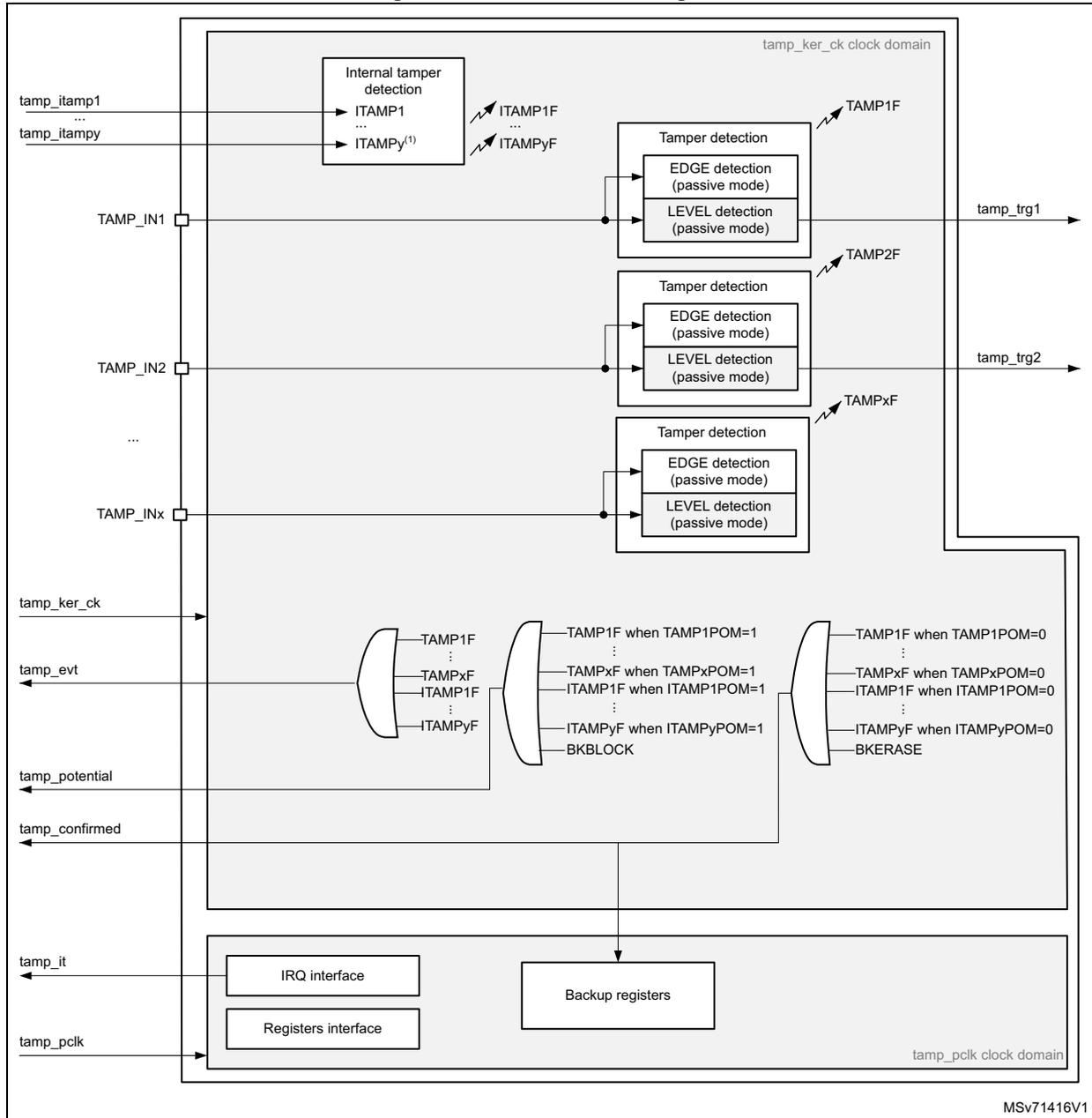
The diagram illustrates the internal architecture of the TAMP block, divided into two clock domains: tamp_ker_ck (top) and tamp_pclk (bottom).
- Inputs:
- tamp_itamp1 to tamp_itampy : Internal tamper signals.
- TAMP_IN1 , TAMP_IN2 , ..., TAMP_INx : External tamper inputs.
- tamp_ker_ck : Core clock input.
- tamp_pclk : Peripheral clock input.
- Internal Tamper Detection:
- A block labeled "Internal tamper detection" receives tamp_itamp1 through tamp_itampy and outputs ITAMP1F , ..., ITAMPyF .
- External Tamper Detection:
- Each external input ( TAMP_IN1 , TAMP_IN2 , ..., TAMP_INx ) is connected to a "Tamper detection" block.
- Each block contains "EDGE detection (passive mode)" and "LEVEL detection (passive mode)".
- Outputs include TAMP1F , TAMP2F , ..., TAMPxF .
- Trigger outputs tamp_trg1 and tamp_trg2 are also shown.
- Logic and Event Generation:
- Signals TAMP1F , ..., TAMPxF , ITAMP1F , ..., ITAMPyF , and BKBLOCK are inputs to a series of AND/OR gates.
- The first gate outputs tamp_evt .
- Subsequent gates generate intermediate signals such as "TAMP1F when TAMP1POM=1", "TAMPxF when TAMPxPOM=1", "ITAMP1F when ITAMP1POM=1", "ITAMPyF when ITAMPyPOM=1", "TAMP1F when TAMP1POM=0", "TAMPxF when TAMPxPOM=0", "ITAMP1F when ITAMP1POM=0", "ITAMPyF when ITAMPyPOM=0", and "BKERASE".
- These intermediate signals are combined to generate tamp_potential and tamp_confirmed .
- Interfaces:
- The tamp_it signal connects to an "IRQ interface" and a "Registers interface".
- Both interfaces connect to "Backup registers".
MSV71416V1
1. The number of external and internal tampers depends on products.
32.3.2 TAMP pins and internal signals
Table 179. TAMP input/output pins
| Pin name | Signal type | Description |
|---|---|---|
| TAMP_INx (x = pin index) | Input | Tamper input pin |
Table 180. TAMP internal input/output signals
| Internal signal name | Signal type | Description |
|---|---|---|
| tamp_ker_ck | Input | TAMP kernel clock, connected to rtc_ker_ck and also named RTCCLK in this document |
| tamp_pclk | Input | TAMP APB clock, connected to rtc_pclk |
| tamp_itamp[y] (y = signal index) | Inputs | Internal tamper event sources |
| tamp_evt | Output | Tamper event detection flag (internal or external tamper), whatever confirmed or potential mode configuration. |
| tamp_potential | Output | Potential tamper detection signal, used for device secrets
(1)
protection. This signal is active when: – a tamper event detection flag (internal or external tamper), is generated in potential mode. – or a software request is done by writing BKBLOCK to 1 |
| tamp_confirmed | Output | Confirmed tamper detection signal, used for device secrets
(1)
protection. This signal is active when: – a tamper event detection flag (internal or external tamper), is generated in confirmed mode. – or a software request is done by writing BKERASE to 1 |
| tamp_it | Output | TAMP interrupt (refer to Section 32.5: TAMP interrupts for details) |
| tamp_trg[x] (x = signal index) | Output | Tamper detection trigger |
- 1. Refer to Table 181: TAMP interconnection .
The TAMP kernel clock is usually the LSE at 32.768 kHz although it is possible to select other clock sources in the RCC (refer to RCC for more details). The TAMP kernel clock is required only for external tamper inputs level with filtering, and for external active tamper detection modes. Internal tampers detection and external tampers inputs edge detection are functional without requiring any kernel clock.
Read and write access to backup registers and all other TAMP registers are also functional without any kernel clock (only APB clock is needed).
Some detections modes are not available in some low-power modes or V BAT depending on the selected clock (refer to Section 32.4: TAMP low-power modes for more details).
Table 181. TAMP interconnection
| Signal name | Source/Destination |
|---|---|
| tamp_evt | rtc_tamp_evt used to generate a timestamp event |
| tamp_potential | The tamp_potential signal is used to block the read and write accesses to the device secrets listed hereafter: – backup registers – BKPRAM |
| tamp_confirmed | The tamp_confirmed signal is used to erase the device secrets listed hereafter: – backup registers – BKPRAM The device secrets access is blocked when erase is ongoing. |
| tamp_itamp3 | LSE monitoring (LSECSS) (1) |
| tamp_itamp4 | HSE monitoring (CSS) (2) |
| tamp_itamp5 | RTC calendar overflow (rtc_calovf) |
| tamp_itamp6 | ST manufacturer readout |
1. This monitoring must be enabled by setting LSECSSON in RTC domain control register (RCC_BDCR) .
2. This monitoring must be enabled by setting HSECSSON in RCC control register (RCC_CR).
32.3.3 GPIOs controlled by the RTC and TAMP
Refer to Section 31.3.3: GPIOs controlled by the RTC and TAMP .
32.3.4 TAMP register write protection
After system reset, the TAMP registers (including backup registers) are protected against parasitic write access by the DBP bit in the power control peripheral (refer to the PWR power control section). DBP bit must be set in order to enable TAMP registers write access.
32.3.5 Tamper detection
The tamper detection main purpose is to protect the device secrets from device external attacks. The detection is made on events on TAMP_INx (x = pin index) I/Os, or on internal monitors detecting out-of-range device conditions.
The tamper detection can be configured for the following purposes:
- • erase the backup registers and other device secrets stored in SRAMs or peripherals listed in Table 181: TAMP interconnection
- • block the read/write access to the backup registers and other device secrets stored in SRAMs or peripherals listed in Table 181: TAMP interconnection
- • generate an interrupt, capable to wake-up from low-power modes
- • generate a hardware trigger for the low-power timers, or a RTC timestamp event
The external I/Os tamper detection supports passive mode: TAMP_INx I/Os are monitored and a tamper is detected either on edge or level.
A digital filter can be applied on external tamper detection to avoid false detection. In addition, it is possible to configure each tamper source in potential mode, so that the secrets erase is not launched by hardware on tamper detection. The secrets erase can then be launched by software after software checks.
32.3.6 TAMP backup registers and other device secrets erase
The backup registers (TAMP_BKPxR) are not reset by system reset or when the device wakes up from Standby mode.
The backup registers and the other device secrets are not reset when the corresponding mask is set (TAMPxMSK=1 in the TAMP_CR2 register).
Note: The backup registers are also erased when the readout protection of the flash is changed from level 1 to level 0.
Tamper detection – confirmed mode
The confirmed mode is selected for TAMPx (external tamper x) when TAMPxPOM = 0 in the TAMP_CR2 register. The confirmed mode is selected for ITAMPx (internal tamper x) when ITAMPxPOM = 0 in the TAMP_CR3 register. The effects of a tamper detection in confirmed mode are described with tamp_confirmed signal in the Table 181: TAMP interconnection .
This mode is selected to erase automatically the device secrets when the tamper is detected.
Tamper detection – potential mode
The potential mode is selected for TAMPx (external tamper x) when TAMPxPOM = 1 in the TAMP_CR2 register. The potential tamper mode is selected for ITAMPx (internal tamper x) when ITAMPxPOM = 1 in the TAMP_CR3 register. The effects of a tamper detection in potential mode are described with tamp_potential signal in the Table 181: TAMP interconnection .
This mode is selected to avoid irreversible erasure of some device secrets when the tamper is detected. In this mode, some device secrets are not erased when the corresponding tamper event is detected. In addition, the read and write accesses to these device secrets are blocked as soon as the tamper detection flag is set in potential mode, until this flag is cleared by setting the corresponding clear flag in the TAMP_SCR register. Therefore the software can perform some checks to discriminate false from true tampers, and decide to launch secrets erase only in case of the potential tamper is confirmed to be a true tamper. The device secrets are erased by software by setting the BKERASE bit in the TAMP_CR2 register.
Potential tamper to confirmed tamper timeout
Some internal tampers generate a tamper event if the independent watchdog reset occurs when another tamper flag is set (refer to Table 181: TAMP interconnection ). The IWDG tamper must be configured with ITAMPxPOM = 0. This permits the erasure of device secrets to be forced by hardware after a timeout, in case the previous tamper event was in potential mode. This is equivalent to change the “potential tamper” into “confirmed tamper” if a watchdog reset occurs before any software decision following the potential tamper event.
Device secrets access blocked by software
By default, the device secrets can be accessed by the application, except if a tamper event flag is detected: the device secrets access is not possible as long as a tamper flag is set.
It is possible to block the access to the device secrets by software, by setting the BKBLOCK bit of the TAMP_CR2 register. The device secrets access is possible only when BKBLOCK = 0 and no tamper flag is set.
32.3.7 Tamper detection configuration and initialization
Each input can be enabled by setting the corresponding TAMPxE bits to 1 in the TAMP_CR register.
Each TAMP_INx tamper detection input is associated with a flag TAMPxF in the TAMP_SR register.
By setting the TAMPxE bit in the TAMP_IER register, an interrupt is generated when a tamper detection event occurs (when TAMPxF is set). Setting TAMPxE is not allowed when the corresponding TAMPxMSK is set.
Trigger output generation on tamper event
The tamper event detection can be used as trigger input by the low-power timers.
When TAMPxMSK bit is cleared in TAMP_CR register, the TAMPxF flag must be cleared by software in order to allow a new tamper detection on the same pin.
When TAMPxMSK bit is set, the TAMPxF flag is masked, and kept cleared in TAMP_SR register. This configuration permits the low-power timers to be triggered automatically in Stop mode, without requiring the system wake-up to perform the TAMPxF clearing. In this case, the backup registers are not cleared.
This feature is available only when the tamper is configured in level detection with filtering mode (TAMPFLT ≠ 00). Refer to Section : Level detection with filtering on tamper inputs (passive mode) .
Timestamp on tamper event
With TAMPTS set to 1 in the RTC_CR, any internal or external tamper event causes a timestamp to occur. In case a timestamp occurs due to tamper event, either the TSF bit or the TSOVF bit is set in RTC_SR, in the same manner as if a normal timestamp event occurs.
Note: TSF is set up to 3 ck_apre cycles after TAMPxF flags. TSF is not set if RTCCLK is stopped (it is set when RTCCLK restarts).
Note: If TAMPxF is cleared before the expected rise of TSF, TSF is not set. Consequently, in case TAMPTS = 1, the software should either wait for timestamp flag before clearing the tamper flag, or should read the RTC counters values in the TAMP interrupt routine.
Edge detection on tamper inputs (passive mode)
If the TAMPFLT bits are 00, the TAMP_INx pins generate tamper detection events when either a rising edge or a falling edge is observed depending on the corresponding TAMPxTRG bit. The internal pull-up resistors on the TAMP_INx inputs are deactivated when edge detection is selected.
Caution: When TAMPFLT = 00 and TAMPxTRG = 0 (rising edge detection), a tamper event may be detected by hardware if the tamper input is already at high level before enabling the tamper detection.
After a tamper event has been detected and cleared, the TAMP_INx should be disabled and then re-enabled (TAMPxE set to 1) before re-programming the backup registers (TAMP_BKPxR). This prevents the application from writing to the backup registers while the TAMP_INx input value still indicates a tamper detection. This is equivalent to a level detection on the TAMP_INx input.
Note: Tamper detection is still active when \( V_{DD} \) power is switched off. To avoid unwanted resetting of the backup registers, the pin to which the TAMPx is mapped should be externally tied to the correct level.
Level detection with filtering on tamper inputs (passive mode)
Level detection with filtering is performed by setting TAMPFLT to a non-zero value. A tamper detection event is generated when either 2, 4, or 8 (depending on TAMPFLT) consecutive samples are observed at the level designated by the TAMPxTRG bits.
The TAMP_INx inputs are precharged through the I/O internal pull-up resistance before its state is sampled, unless disabled by setting TAMPPUDIS to 1. The duration of the precharge is determined by the TAMPPRCH bits, allowing for larger capacitances on the TAMP_INx inputs.
The trade-off between tamper detection latency and power consumption through the pull-up can be optimized by using TAMPFREQ to determine the frequency of the sampling for level detection. The TAMP_IN I/O schmitt trigger is enabled only during the precharge duration to avoid any extra consumption if the tamper switch is open (floating state).
Figure 302. Tamper sampling with precharge pulse
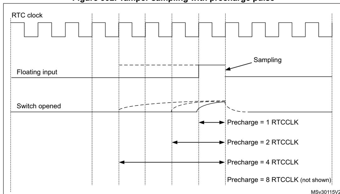
The figure is a timing diagram with three horizontal signal lines. The top line is labeled 'RTC clock' and shows a periodic square wave. The middle line is labeled 'Floating input' and shows a dashed line that starts at a high level and begins to drop when the switch is opened. The bottom line is labeled 'Switch opened' and shows a solid line that starts at a low level and jumps to a high level when the switch is opened. Vertical dashed lines mark the rising edges of the RTC clock. A horizontal arrow labeled 'Sampling' points to a high level of the Floating input coinciding with a high level of the RTC clock. Four horizontal double-headed arrows indicate precharge durations: 'Precharge = 1 RTCCLK' (one clock period), 'Precharge = 2 RTCCLK' (two clock periods), 'Precharge = 4 RTCCLK' (four clock periods), and 'Precharge = 8 RTCCLK (not shown)' (eight clock periods). The diagram is labeled 'MSV30115V2' in the bottom right corner.
Figure 303. Low level detection with precharge and filtering
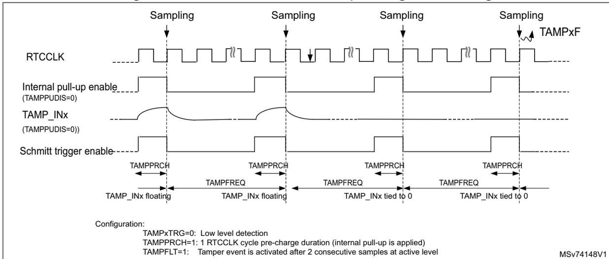
Configuration:
TAMPxTRG=0: Low level detection
TAMPPRCH=1: 1 RTCCLK cycle pre-charge duration (internal pull-up is applied)
TAMPFLT=1: Tamper event is activated after 2 consecutive samples at active level
MSV74148V1
Note: Refer to the microcontroller datasheet for the electrical characteristics of the pull-up resistors.
32.4 TAMP low-power modes
Table 182. Effect of low-power modes on TAMP
| Mode | Description |
|---|---|
| Sleep | No effect. TAMP interrupts cause the device to exit the Sleep mode. |
| Stop | No effect on all features, except for level detection with filtering mode which remain active only when the clock source is LSE or LSI. TAMP interrupts cause the device to exit the Stop mode. |
| Standby | No effect on all features, except for level detection with filtering mode which remain active only when the clock source is LSE or LSI. TAMP interrupts cause the device to exit the Standby mode. |
| Shutdown | No effect on all features, except for level detection with filtering mode which remain active only when the clock source is LSE. TAMP interrupts cause the device to exit the Shutdown mode. |
Table 183. TAMP pins functionality over modes
| Pin name | Functional in all low-power modes | Functional in V BAT mode |
|---|---|---|
| TAMP_IN[5:0] | Yes | Yes |
32.5 TAMP interrupts
Table 184. Interrupt requests
| Interrupt acronym | Interrupt event | Event flag (1) | Enable control bit | Interrupt clear method | Exit from low-power modes |
|---|---|---|---|---|---|
| TAMP | Tamper x (2) | TAMPxF | TAMPxE | Write 1 in CTAMPxF | Yes (3) |
| Internal tamper y (2) | ITAMPyF | ITAMPyE | Write 1 in CITAMPyF | Yes (3) |
- 1. The event flags are in the TAMP_SR register.
- 2. The number of tampers and internal tampers events depend on products.
- 3. Refer to Table 182: Effect of low-power modes on TAMP for more details about available features in the low-power modes.
32.6 TAMP registers
Refer to Section 1.2 of the reference manual for a list of abbreviations used in register descriptions. The peripheral registers can be accessed by words (32-bit).
32.6.1 TAMP control register 1 (TAMP_CR1)
Address offset: 0x00
Backup domain reset value: 0x0000 0000
System reset: not affected
| 31 | 30 | 29 | 28 | 27 | 26 | 25 | 24 | 23 | 22 | 21 | 20 | 19 | 18 | 17 | 16 |
|---|---|---|---|---|---|---|---|---|---|---|---|---|---|---|---|
| Res. | Res. | Res. | Res. | Res. | Res. | Res. | Res. | Res. | Res. | ITAMP6 E | ITAMP5 E | ITAMP4 E | ITAMP3 E | Res. | Res. |
| rw | rw | rw | rw |
| 15 | 14 | 13 | 12 | 11 | 10 | 9 | 8 | 7 | 6 | 5 | 4 | 3 | 2 | 1 | 0 |
|---|---|---|---|---|---|---|---|---|---|---|---|---|---|---|---|
| Res. | Res. | Res. | Res. | Res. | Res. | Res. | Res. | Res. | Res. | Res. | TAMP5 E | TAMP4 E | TAMP3 E | TAMP2 E | TAMP1 E |
| rw | rw | rw | rw | rw |
Bit 31 Reserved, must be kept at reset value.
Bit 30 Reserved, must be kept at reset value.
Bit 29 Reserved, must be kept at reset value.
Bit 28 Reserved, must be kept at reset value.
Bit 27 Reserved, must be kept at reset value.
Bit 26 Reserved, must be kept at reset value.
Bit 25 Reserved, must be kept at reset value.
Bit 24 Reserved, must be kept at reset value.
Bit 23 Reserved, must be kept at reset value.
- Bit 22 Reserved, must be kept at reset value.
- Bit 21
ITAMP6E
: Internal tamper 6 enable
0: Internal tamper 6 disabled.
1: Internal tamper 6 enabled. - Bit 20
ITAMP5E
: Internal tamper 5 enable
0: Internal tamper 5 disabled.
1: Internal tamper 5 enabled. - Bit 19
ITAMP4E
: Internal tamper 4 enable
0: Internal tamper 4 disabled.
1: Internal tamper 4 enabled. - Bit 18
ITAMP3E
: Internal tamper 3 enable
0: Internal tamper 3 disabled.
1: Internal tamper 3 enabled. - Bit 17 Reserved, must be kept at reset value.
- Bit 16 Reserved, must be kept at reset value.
- Bits 15:8 Reserved, must be kept at reset value.
- Bit 7 Reserved, must be kept at reset value.
- Bit 6 Reserved, must be kept at reset value.
- Bit 5 Reserved, must be kept at reset value.
- Bit 4
TAMP5E
: Tamper detection on TAMP_IN5 enable
(1)
0: Tamper detection on TAMP_IN5 is disabled.
1: Tamper detection on TAMP_IN5 is enabled. - Bit 3
TAMP4E
: Tamper detection on TAMP_IN4 enable
(1)
0: Tamper detection on TAMP_IN4 is disabled.
1: Tamper detection on TAMP_IN4 is enabled. - Bit 2
TAMP3E
: Tamper detection on TAMP_IN3 enable
(1)
0: Tamper detection on TAMP_IN3 is disabled.
1: Tamper detection on TAMP_IN3 is enabled. - Bit 1
TAMP2E
: Tamper detection on TAMP_IN2 enable
(1)
0: Tamper detection on TAMP_IN2 is disabled.
1: Tamper detection on TAMP_IN2 is enabled. - Bit 0
TAMP1E
: Tamper detection on TAMP_IN1 enable
(1)
0: Tamper detection on TAMP_IN1 is disabled.
1: Tamper detection on TAMP_IN1 is enabled.
- 1. Tamper detection mode (selected with TAMP_FLTCR register and TAMPxTRG bits in TAMP_CR2), must be configured before enabling the tamper detection.
32.6.2 TAMP control register 2 (TAMP_CR2)
Address offset: 0x04
Backup domain reset value: 0x0000 0000
System reset: not affected
| 31 | 30 | 29 | 28 | 27 | 26 | 25 | 24 | 23 | 22 | 21 | 20 | 19 | 18 | 17 | 16 |
|---|---|---|---|---|---|---|---|---|---|---|---|---|---|---|---|
| Res. | Res. | Res. | TAMP5 TRG | TAMP4 TRG | TAMP3 TRG | TAMP2 TRG | TAMP1 TRG | BK ERASE | BK BLOCK | Res. | Res. | Res. | TAMP3 MSK | TAMP2 MSK | TAMP1 MSK |
| rw | rw | rw | rw | rw | w | rw | rw | rw | rw | ||||||
| 15 | 14 | 13 | 12 | 11 | 10 | 9 | 8 | 7 | 6 | 5 | 4 | 3 | 2 | 1 | 0 |
| Res. | Res. | Res. | Res. | Res. | Res. | Res. | Res. | Res. | Res. | Res. | TAMP5 POM | TAMP4 POM | TAMP3 POM | TAMP2 POM | TAMP1 POM |
| rw | rw | rw | rw | rw |
Bit 31 Reserved, must be kept at reset value.
Bit 30 Reserved, must be kept at reset value.
Bit 29 Reserved, must be kept at reset value.
Bit 28 TAMP5TRG : Active level for tamper 5 input (active mode disabled)
- 0: If TAMPFLT ≠ 00 tamper 5 input staying low triggers a tamper detection event.
If TAMPFLT = 00 tamper 5 input rising edge triggers a tamper detection event. - 1: If TAMPFLT ≠ 00 tamper 5 input staying high triggers a tamper detection event.
If TAMPFLT = 00 tamper 5 input falling edge triggers a tamper detection event.
Bit 27 TAMP4TRG : Active level for tamper 4 input (active mode disabled)
- 0: If TAMPFLT ≠ 00 tamper 4 input staying low triggers a tamper detection event.
If TAMPFLT = 00 tamper 4 input rising edge triggers a tamper detection event. - 1: If TAMPFLT ≠ 00 tamper 4 input staying high triggers a tamper detection event.
If TAMPFLT = 00 tamper 4 input falling edge triggers a tamper detection event.
Bit 26 TAMP3TRG : Active level for tamper 3 input
- 0: If TAMPFLT ≠ 00 tamper 3 input staying low triggers a tamper detection event.
If TAMPFLT = 00 tamper 3 input rising edge triggers a tamper detection event. - 1: If TAMPFLT ≠ 00 tamper 3 input staying high triggers a tamper detection event.
If TAMPFLT = 00 tamper 3 input falling edge triggers a tamper detection event.
Bit 25 TAMP2TRG : Active level for tamper 2 input
- 0: If TAMPFLT ≠ 00 tamper 2 input staying low triggers a tamper detection event.
If TAMPFLT = 00 tamper 2 input rising edge triggers a tamper detection event. - 1: If TAMPFLT ≠ 00 tamper 2 input staying high triggers a tamper detection event.
If TAMPFLT = 00 tamper 2 input falling edge triggers a tamper detection event.
Bit 24 TAMP1TRG : Active level for tamper 1 input
- 0: If TAMPFLT ≠ 00 tamper 1 input staying low triggers a tamper detection event.
If TAMPFLT = 00 tamper 1 input rising edge triggers a tamper detection event. - 1: If TAMPFLT ≠ 00 tamper 1 input staying high triggers a tamper detection event.
If TAMPFLT = 00 tamper 1 input falling edge triggers a tamper detection event.
Bit 23 BKERASE : Backup registers and device secrets (1) erase
Writing '1' to this bit reset the backup registers and device secrets (1) . Writing 0 has no effect. This bit is always read as 0.
Bit 22 BKBLOCK : Backup registers and device secrets (1) access blocked
0: backup registers and device secrets (1) can be accessed if no tamper flag is set
1: backup registers and device secrets (1) cannot be accessed
Bits 21:19 Reserved, must be kept at reset value.
Bit 18 TAMP3MSK : Tamper 3 mask
0: Tamper 3 event generates a trigger event and TAMP3F must be cleared by software to allow next tamper event detection.
1: Tamper 3 event generates a trigger event. TAMP3F is masked and internally cleared by hardware. The backup registers and device secrets (1) are not erased.
The tamper 3 interrupt must not be enabled when TAMP3MSK is set.
Bit 17 TAMP2MSK : Tamper 2 mask
0: Tamper 2 event generates a trigger event and TAMP2F must be cleared by software to allow next tamper event detection.
1: Tamper 2 event generates a trigger event. TAMP2F is masked and internally cleared by hardware. The backup registers and device secrets (1) are not erased.
The tamper 2 interrupt must not be enabled when TAMP2MSK is set.
Bit 16 TAMP1MSK : Tamper 1 mask
0: Tamper 1 event generates a trigger event and TAMP1F must be cleared by software to allow next tamper event detection.
1: Tamper 1 event generates a trigger event. TAMP1F is masked and internally cleared by hardware. The backup registers and device secrets (1) are not erased.
The tamper 1 interrupt must not be enabled when TAMP1MSK is set.
Bits 15:8 Reserved, must be kept at reset value.
Bit 7 Reserved, must be kept at reset value.
Bit 6 Reserved, must be kept at reset value.
Bit 5 Reserved, must be kept at reset value.
Bit 4 TAMP5POM : Tamper 5 potential mode
0: Tamper 5 event detection is in confirmed mode (1) .
1: Tamper 5 event detection is in potential mode (2) .
Bit 3 TAMP4POM : Tamper 4 potential mode
0: Tamper 4 event detection is in confirmed mode (1) .
1: Tamper 4 event detection is in potential mode (2) .
Bit 2 TAMP3POM : Tamper 3 potential mode
0: Tamper 3 event detection is in confirmed mode (1) .
1: Tamper 3 event detection is in potential mode (2) .
Bit 1 TAMP2POM : Tamper 2 potential mode
0: Tamper 2 event detection is in confirmed mode (1) .
1: Tamper 2 event detection is in potential mode (2) .
Bit 0 TAMP1POM : Tamper 1 potential mode
0: Tamper 1 event detection is in confirmed mode (1) .
1: Tamper 1 event detection is in potential mode (2) .
- 1. The effects of tamper detection in confirmed mode is described with
tamp_confirmedsignal in Table 181: TAMP interconnection . - 2. The effects of tamper detection in potential mode is described with
tamp_potentialsignal in Table 181: TAMP interconnection .
32.6.3 TAMP control register 3 (TAMP_CR3)
Address offset: 0x08
Backup domain reset value: 0x0000 0000
System reset: not affected
| 31 | 30 | 29 | 28 | 27 | 26 | 25 | 24 | 23 | 22 | 21 | 20 | 19 | 18 | 17 | 16 |
|---|---|---|---|---|---|---|---|---|---|---|---|---|---|---|---|
| Res. | Res. | Res. | Res. | Res. | Res. | Res. | Res. | Res. | Res. | Res. | Res. | Res. | Res. | Res. | Res. |
| 15 | 14 | 13 | 12 | 11 | 10 | 9 | 8 | 7 | 6 | 5 | 4 | 3 | 2 | 1 | 0 |
| Res. | Res. | Res. | Res. | Res. | Res. | Res. | Res. | Res. | Res. | ITAMP6 POM | ITAMP5 POM | ITAMP4 POM | ITAMP3 POM | Res. | Res. |
| rw | rw | rw | rw |
Bits 31:16 Reserved, must be kept at reset value.
Bit 15 Reserved, must be kept at reset value.
Bit 14 Reserved, must be kept at reset value.
Bit 13 Reserved, must be kept at reset value.
Bit 12 Reserved, must be kept at reset value.
Bit 11 Reserved, must be kept at reset value.
Bit 10 Reserved, must be kept at reset value.
Bit 9 Reserved, must be kept at reset value.
Bit 8 Reserved, must be kept at reset value.
Bit 7 Reserved, must be kept at reset value.
Bit 6 Reserved, must be kept at reset value.
Bit 5 ITAMP6POM : Internal tamper 6 potential mode
0: Internal tamper 6 event detection is in confirmed mode (1) .
1: Internal tamper 6 event detection is in potential mode (2) .
Bit 4 ITAMP5POM : Internal tamper 5 potential mode
0: Internal tamper 5 event detection is in confirmed mode (1) .
1: Internal tamper 5 event detection is in potential mode (2) .
Bit 3 ITAMP4POM : Internal tamper 4 potential mode
0: Internal tamper 4 event detection is in confirmed mode (1) .
1: Internal tamper 4 event detection is in potential mode (2) .
Bit 2 ITAMP3POM : Internal tamper 3 potential mode
0: Internal tamper 3 event detection is in confirmed mode (1) .
1: Internal tamper 3 event detection is in potential mode (2) .
Bit 1 Reserved, must be kept at reset value.
Bit 0 Reserved, must be kept at reset value.
1. The effects of internal tamper detection in confirmed mode is described with tamp_confirmed signal in Table 181: TAMP interconnection
2. The effects of internal tamper detection in potential mode is described with tamp_potential signal in Table 181: TAMP interconnection .
32.6.4 TAMP filter control register (TAMP_FLTCR)
Address offset: 0x0C
Backup domain reset value: 0x0000 0000
System reset: not affected
| 31 | 30 | 29 | 28 | 27 | 26 | 25 | 24 | 23 | 22 | 21 | 20 | 19 | 18 | 17 | 16 |
|---|---|---|---|---|---|---|---|---|---|---|---|---|---|---|---|
| Res. | Res. | Res. | Res. | Res. | Res. | Res. | Res. | Res. | Res. | Res. | Res. | Res. | Res. | Res. | Res. |
| 15 | 14 | 13 | 12 | 11 | 10 | 9 | 8 | 7 | 6 | 5 | 4 | 3 | 2 | 1 | 0 |
| Res. | Res. | Res. | Res. | Res. | Res. | Res. | Res. | TAMP PUDIS | TAMPPRCH [1:0] | TAMPFLT [1:0] | TAMPFREQ [2:0] | ||||
| rw | rw | rw | rw | rw | rw | rw | rw | ||||||||
Bits 31:8 Reserved, must be kept at reset value.
Bit 7 TAMPPUDIS : TAMP_INx pull-up disable
This bit determines if each of the TAMPx pins are precharged before each sample.
0: Precharge TAMP_INx pins before sampling (enable internal pull-up)
1: Disable precharge of TAMP_INx pins.
Bits 6:5 TAMPPRCH[1:0] : TAMP_INx precharge duration
These bits determine the duration of time during which the pull-up/is activated before each sample. TAMPPRCH is valid for each of the TAMP_INx inputs.
0x0: 1 RTCCLK cycle
0x1: 2 RTCCLK cycles
0x2: 4 RTCCLK cycles
0x3: 8 RTCCLK cycles
Bits 4:3 TAMPFLT[1:0] : TAMP_INx filter count
These bits determine the number of consecutive samples at the specified level (TAMP*TRG) needed to activate a tamper event. TAMPFLT is valid for each of the TAMP_INx inputs.
0x0: Tamper event is activated on edge of TAMP_INx input transitions to the active level (no internal pull-up on TAMP_INx input).
0x1: Tamper event is activated after 2 consecutive samples at the active level.
0x2: Tamper event is activated after 4 consecutive samples at the active level.
0x3: Tamper event is activated after 8 consecutive samples at the active level.
Bits 2:0 TAMPFREQ[2:0] : Tamper sampling frequency
Determines the frequency at which each of the TAMP_INx inputs are sampled.
0x0: RTCCLK / 32768 (1 Hz when RTCCLK = 32768 Hz)
0x1: RTCCLK / 16384 (2 Hz when RTCCLK = 32768 Hz)
0x2: RTCCLK / 8192 (4 Hz when RTCCLK = 32768 Hz)
0x3: RTCCLK / 4096 (8 Hz when RTCCLK = 32768 Hz)
0x4: RTCCLK / 2048 (16 Hz when RTCCLK = 32768 Hz)
0x5: RTCCLK / 1024 (32 Hz when RTCCLK = 32768 Hz)
0x6: RTCCLK / 512 (64 Hz when RTCCLK = 32768 Hz)
0x7: RTCCLK / 256 (128 Hz when RTCCLK = 32768 Hz)
Note: This register concerns only the tamper inputs in passive mode.
32.6.5 TAMP interrupt enable register (TAMP_IER)
Address offset: 0x2C
Backup domain reset value: 0x0000 0000
System reset: not affected
| 31 | 30 | 29 | 28 | 27 | 26 | 25 | 24 | 23 | 22 | 21 | 20 | 19 | 18 | 17 | 16 |
|---|---|---|---|---|---|---|---|---|---|---|---|---|---|---|---|
| Res. | Res. | Res. | Res. | Res. | Res. | Res. | Res. | Res. | Res. | ITAMP6 IE | ITAMP5 IE | ITAMP4 IE | ITAMP3 IE | Res. | Res. |
| rw | rw | rw | rw |
| 15 | 14 | 13 | 12 | 11 | 10 | 9 | 8 | 7 | 6 | 5 | 4 | 3 | 2 | 1 | 0 |
|---|---|---|---|---|---|---|---|---|---|---|---|---|---|---|---|
| Res. | Res. | Res. | Res. | Res. | Res. | Res. | Res. | Res. | Res. | Res. | TAMP 5IE | TAMP 4IE | TAMP 3IE | TAMP 2IE | TAMP 1IE |
| rw | rw | rw | rw | rw |
Bit 31 Reserved, must be kept at reset value.
Bit 30 Reserved, must be kept at reset value.
Bit 29 Reserved, must be kept at reset value.
Bit 28 Reserved, must be kept at reset value.
Bit 27 Reserved, must be kept at reset value.
Bit 26 Reserved, must be kept at reset value.
Bit 25 Reserved, must be kept at reset value.
Bit 24 Reserved, must be kept at reset value.
Bit 23 Reserved, must be kept at reset value.
Bit 22 Reserved, must be kept at reset value.
Bit 21 ITAMP6IE : Internal tamper 6 interrupt enable
0: Internal tamper 6 interrupt disabled.
1: Internal tamper 6 interrupt enabled.
Bit 20 ITAMP5IE : Internal tamper 5 interrupt enable
0: Internal tamper 5 interrupt disabled.
1: Internal tamper 5 interrupt enabled.
Bit 19 ITAMP4IE : Internal tamper 4 interrupt enable
0: Internal tamper 4 interrupt disabled.
1: Internal tamper 4 interrupt enabled.
Bit 18 ITAMP3IE : Internal tamper 3 interrupt enable
0: Internal tamper 3 interrupt disabled.
1: Internal tamper 3 interrupt enabled.
Bit 17 Reserved, must be kept at reset value.
Bit 16 Reserved, must be kept at reset value.
Bits 15:8 Reserved, must be kept at reset value.
Bit 7 Reserved, must be kept at reset value.
Bit 6 Reserved, must be kept at reset value.
Bit 5 Reserved, must be kept at reset value.
- Bit 4
TAMP5IE
: Tamper 5 interrupt enable
- 0: Tamper 5 interrupt disabled.
- 1: Tamper 5 interrupt enabled.
- Bit 3
TAMP4IE
: Tamper 4 interrupt enable
- 0: Tamper 4 interrupt disabled.
- 1: Tamper 4 interrupt enabled.
- Bit 2
TAMP3IE
: Tamper 3 interrupt enable
- 0: Tamper 3 interrupt disabled.
- 1: Tamper 3 interrupt enabled..
- Bit 1
TAMP2IE
: Tamper 2 interrupt enable
- 0: Tamper 2 interrupt disabled.
- 1: Tamper 2 interrupt enabled.
- Bit 0
TAMP1IE
: Tamper 1 interrupt enable
- 0: Tamper 1 interrupt disabled.
- 1: Tamper 1 interrupt enabled.
32.6.6 TAMP status register (TAMP_SR)
Address offset: 0x30
Backup domain reset value: 0x0000 0000
System reset: not affected
| 31 | 30 | 29 | 28 | 27 | 26 | 25 | 24 | 23 | 22 | 21 | 20 | 19 | 18 | 17 | 16 |
|---|---|---|---|---|---|---|---|---|---|---|---|---|---|---|---|
| Res. | Res. | Res. | Res. | Res. | Res. | Res. | Res. | Res. | Res. | ITAMP6 F | ITAMP5 F | ITAMP4 F | ITAMP3 F | Res. | Res. |
| r | r | r | r | ||||||||||||
| 15 | 14 | 13 | 12 | 11 | 10 | 9 | 8 | 7 | 6 | 5 | 4 | 3 | 2 | 1 | 0 |
| Res. | Res. | Res. | Res. | Res. | Res. | Res. | Res. | Res. | Res. | Res. | TAMP 5F | TAMP 4F | TAMP 3F | TAMP 2F | TAMP 1F |
| r | r | r | r | r |
- Bit 31 Reserved, must be kept at reset value.
- Bit 30 Reserved, must be kept at reset value.
- Bit 29 Reserved, must be kept at reset value.
- Bit 28 Reserved, must be kept at reset value.
- Bit 27 Reserved, must be kept at reset value.
- Bit 26 Reserved, must be kept at reset value.
- Bit 25 Reserved, must be kept at reset value.
- Bit 24 Reserved, must be kept at reset value.
- Bit 23 Reserved, must be kept at reset value.
- Bit 22 Reserved, must be kept at reset value.
- Bit 21
ITAMP6F
: Internal tamper 6 flag
- This flag is set by hardware when a tamper detection event is detected on the internal tamper 6.
Bit 20 ITAMP5F : Internal tamper 5 flag
This flag is set by hardware when a tamper detection event is detected on the internal tamper 5.
Bit 19 ITAMP4F : Internal tamper 4 flag
This flag is set by hardware when a tamper detection event is detected on the internal tamper 4.
Bit 18 ITAMP3F : Internal tamper 3 flag
This flag is set by hardware when a tamper detection event is detected on the internal tamper 3.
Bit 17 Reserved, must be kept at reset value.
Bit 16 Reserved, must be kept at reset value.
Bits 15:8 Reserved, must be kept at reset value.
Bit 7 Reserved, must be kept at reset value.
Bit 6 Reserved, must be kept at reset value.
Bit 5 Reserved, must be kept at reset value.
Bit 4 TAMP5F : TAMP5 detection flag
This flag is set by hardware when a tamper detection event is detected on the TAMP5 input.
Bit 3 TAMP4F : TAMP4 detection flag
This flag is set by hardware when a tamper detection event is detected on the TAMP4 input.
Bit 2 TAMP3F : TAMP3 detection flag
This flag is set by hardware when a tamper detection event is detected on the TAMP3 input.
Bit 1 TAMP2F : TAMP2 detection flag
This flag is set by hardware when a tamper detection event is detected on the TAMP2 input.
Bit 0 TAMP1F : TAMP1 detection flag
This flag is set by hardware when a tamper detection event is detected on the TAMP1 input.
32.6.7 TAMP masked interrupt status register (TAMP_MISR)
Address offset: 0x34
Backup domain reset value: 0x0000 0000
System reset: not affected
| 31 | 30 | 29 | 28 | 27 | 26 | 25 | 24 | 23 | 22 | 21 | 20 | 19 | 18 | 17 | 16 |
|---|---|---|---|---|---|---|---|---|---|---|---|---|---|---|---|
| Res. | Res. | Res. | Res. | Res. | Res. | Res. | Res. | Res. | Res. | ITAMP6 MF | ITAMP5 MF | ITAMP4 MF | ITAMP3 MF | Res. | Res. |
| r | r | r | r | ||||||||||||
| 15 | 14 | 13 | 12 | 11 | 10 | 9 | 8 | 7 | 6 | 5 | 4 | 3 | 2 | 1 | 0 |
| Res. | Res. | Res. | Res. | Res. | Res. | Res. | Res. | Res. | Res. | Res. | TAMP 5MF | TAMP 4MF | TAMP 3MF | TAMP 2MF | TAMP 1MF |
| r | r | r | r | r |
Bit 31 Reserved, must be kept at reset value.
Bit 30 Reserved, must be kept at reset value.
Bit 29 Reserved, must be kept at reset value.
- Bit 28 Reserved, must be kept at reset value.
- Bit 27 Reserved, must be kept at reset value.
- Bit 26 Reserved, must be kept at reset value.
- Bit 25 Reserved, must be kept at reset value.
- Bit 24 Reserved, must be kept at reset value.
- Bit 23 Reserved, must be kept at reset value.
- Bit 22 Reserved, must be kept at reset value.
- Bit 21
ITAMP6MF
: Internal tamper 6 interrupt masked flag
This flag is set by hardware when the internal tamper 6 interrupt is raised. - Bit 20
ITAMP5MF
: Internal tamper 5 interrupt masked flag
This flag is set by hardware when the internal tamper 5 interrupt is raised. - Bit 19
ITAMP4MF
: Internal tamper 4 interrupt masked flag
This flag is set by hardware when the internal tamper 4 interrupt is raised. - Bit 18
ITAMP3MF
: Internal tamper 3 interrupt masked flag
This flag is set by hardware when the internal tamper 3 interrupt is raised. - Bit 17 Reserved, must be kept at reset value.
- Bit 16 Reserved, must be kept at reset value.
- Bits 15:8 Reserved, must be kept at reset value.
- Bit 7 Reserved, must be kept at reset value.
- Bit 6 Reserved, must be kept at reset value.
- Bit 5 Reserved, must be kept at reset value.
- Bit 4
TAMP5MF
: TAMP5 interrupt masked flag
This flag is set by hardware when the tamper 5 interrupt is raised. - Bit 3
TAMP4MF
: TAMP4 interrupt masked flag
This flag is set by hardware when the tamper 4 interrupt is raised. - Bit 2
TAMP3MF
: TAMP3 interrupt masked flag
This flag is set by hardware when the tamper 3 interrupt is raised. - Bit 1
TAMP2MF
: TAMP2 interrupt masked flag
This flag is set by hardware when the tamper 2 interrupt is raised. - Bit 0
TAMP1MF
: TAMP1 interrupt masked flag
This flag is set by hardware when the tamper 1 interrupt is raised.
32.6.8 TAMP status clear register (TAMP_SCR)
Address offset: 0x3C
System reset value: 0x0000 0000
| 31 | 30 | 29 | 28 | 27 | 26 | 25 | 24 | 23 | 22 | 21 | 20 | 19 | 18 | 17 | 16 |
|---|---|---|---|---|---|---|---|---|---|---|---|---|---|---|---|
| Res. | Res. | Res. | Res. | Res. | Res. | Res. | Res. | Res. | Res. | C ITAMP 6F | C ITAMP 5F | C ITAMP 4F | C ITAMP 3F | Res. | Res. |
| 15 | 14 | 13 | 12 | 11 | 10 | 9 | 8 | 7 | 6 | 5 | 4 | 3 | 2 | 1 | 0 |
| Res. | Res. | Res. | Res. | Res. | Res. | Res. | Res. | Res. | Res. | Res. | CTAMP 5F | CTAMP 4F | CTAMP 3F | CTAMP 2F | CTAMP 1F |
| w | w | w | w | w |
Bit 31 Reserved, must be kept at reset value.
Bit 30 Reserved, must be kept at reset value.
Bit 29 Reserved, must be kept at reset value.
Bit 28 Reserved, must be kept at reset value.
Bit 27 Reserved, must be kept at reset value.
Bit 26 Reserved, must be kept at reset value.
Bit 25 Reserved, must be kept at reset value.
Bit 24 Reserved, must be kept at reset value.
Bit 23 Reserved, must be kept at reset value.
Bit 22 Reserved, must be kept at reset value.
Bit 21 CITAMP6F : Clear ITAMP6 detection flag
Writing 1 in this bit clears the ITAMP6F bit in the TAMP_SR register.
Bit 20 CITAMP5F : Clear ITAMP5 detection flag
Writing 1 in this bit clears the ITAMP5F bit in the TAMP_SR register.
Bit 19 CITAMP4F : Clear ITAMP4 detection flag
Writing 1 in this bit clears the ITAMP4F bit in the TAMP_SR register.
Bit 18 CITAMP3F : Clear ITAMP3 detection flag
Writing 1 in this bit clears the ITAMP3F bit in the TAMP_SR register.
Bit 17 Reserved, must be kept at reset value.
Bit 16 Reserved, must be kept at reset value.
Bits 15:8 Reserved, must be kept at reset value.
Bit 7 Reserved, must be kept at reset value.
Bit 6 Reserved, must be kept at reset value.
Bit 5 Reserved, must be kept at reset value.
Bit 4 CTAMP5F : Clear TAMP5 detection flag
Writing 1 in this bit clears the TAMP5F bit in the TAMP_SR register.
Bit 3 CTAMP4F : Clear TAMP4 detection flag
Writing 1 in this bit clears the TAMP4F bit in the TAMP_SR register.
- Bit 2
CTAMP3F
: Clear TAMP3 detection flag
Writing 1 in this bit clears the TAMP3F bit in the TAMP_SR register. - Bit 1
CTAMP2F
: Clear TAMP2 detection flag
Writing 1 in this bit clears the TAMP2F bit in the TAMP_SR register. - Bit 0
CTAMP1F
: Clear TAMP1 detection flag
Writing 1 in this bit clears the TAMP1F bit in the TAMP_SR register.
32.6.9 TAMP backup x register (TAMP_BKPxR)
Address offset: 0x100 + 0x04 * x, (x = 0 to 8)
Backup domain reset value: 0x0000 0000
System reset: not affected
| 31 | 30 | 29 | 28 | 27 | 26 | 25 | 24 | 23 | 22 | 21 | 20 | 19 | 18 | 17 | 16 |
| BKP[31:16] | |||||||||||||||
| rw | rw | rw | rw | rw | rw | rw | rw | rw | rw | rw | rw | rw | rw | rw | rw |
| 15 | 14 | 13 | 12 | 11 | 10 | 9 | 8 | 7 | 6 | 5 | 4 | 3 | 2 | 1 | 0 |
| BKP[15:0] | |||||||||||||||
| rw | rw | rw | rw | rw | rw | rw | rw | rw | rw | rw | rw | rw | w | rw | rw |
Bits 31:0 BKP[31:0]:
The application can write or read data to and from these registers.
In the default (ERASE) configuration this register is reset on a tamper detection event. It is forced to reset value as long as there is at least one internal or external tamper flag being set. This register is also reset when the readout protection (RDP) is disabled.
32.6.10 TAMP register map
Table 185. TAMP register map and reset values
| Offset | Register name | 31 | 30 | 29 | 28 | 27 | 26 | 25 | 24 | 23 | 22 | 21 | 20 | 19 | 18 | 17 | 16 | 15 | 14 | 13 | 12 | 11 | 10 | 9 | 8 | 7 | 6 | 5 | 4 | 3 | 2 | 1 | 0 | |
|---|---|---|---|---|---|---|---|---|---|---|---|---|---|---|---|---|---|---|---|---|---|---|---|---|---|---|---|---|---|---|---|---|---|---|
| 0x00 | TAMP_CR1 | Res | Res | Res | Res | Res | Res | Res | Res | Res | Res | ITAMP6E | ITAMP5E | ITAMP4E | ITAMP3E | Res | Res | Res | Res | Res | Res | Res | Res | Res | Res | Res | Res | Res | Res | Res | TAMP5E | TAMP4E | TAMP3E | TAMP2E |
| Reset value | 0 | 0 | 0 | 0 | 0 | 0 | 0 | 0 | ||||||||||||||||||||||||||
| 0x04 | TAMP_CR2 | Res | Res | Res | TAMP5TRG | TAMP4TRG | TAMP3TRG | TAMP2TRG | TAMP1TRG | BKERASE | BKBLOCK | Res | Res | Res | TAMP3MSK | TAMP2MSK | TAMP1MSK | Res | Res | Res | Res | Res | Res | Res | Res | Res | Res | Res | Res | Res | TAMP5POM | TAMP4POM | TAMP3POM | TAMP2POM |
| Reset value | 0 | 0 | 0 | 0 | 0 | 0 | 0 | 0 | 0 | 0 | 0 | 0 | 0 | 0 | ||||||||||||||||||||
| 0x08 | TAMP_CR3 | Res | Res | Res | Res | Res | Res | Res | Res | Res | Res | Res | Res | Res | Res | Res | Res | Res | Res | Res | Res | Res | Res | Res | Res | Res | Res | Res | Res | Res | ITAMP6POM | ITAMP5POM | ITAMP4POM | ITAMP3POM |
| Reset value | 0 | 0 | 0 | 0 | ||||||||||||||||||||||||||||||
| 0x0C | TAMP_FLTCR | Res | Res | Res | Res | Res | Res | Res | Res | Res | Res | Res | Res | Res | Res | Res | Res | Res | Res | Res | Res | Res | Res | Res | Res | TAMPPIUDIS | TAMPPIRCH[1:0] | Res | Res | Res | TAMPLT[1:0] | Res | TAMPFREQ[2:0] | |
| Reset value | 0 | 0 | 0 | 0 | 0 | 0 | ||||||||||||||||||||||||||||
| 0x2C | TAMP_IER | Res | Res | Res | Res | Res | Res | Res | Res | Res | Res | ITAMP6IE | ITAMP5IE | ITAMP4IE | ITAMP3IE | Res | Res | Res | Res | Res | Res | Res | Res | Res | Res | Res | Res | Res | Res | Res | TAMP5IE | TAMP4IE | TAMP3IE | TAMP2IE |
| Reset value | 0 | 0 | 0 | 0 | 0 | 0 | 0 | 0 | ||||||||||||||||||||||||||
| 0x30 | TAMP_SR | Res | Res | Res | Res | Res | Res | Res | Res | Res | Res | ITAMP6F | ITAMP5F | ITAMP4F | ITAMP3F | Res | Res | Res | Res | Res | Res | Res | Res | Res | Res | Res | Res | Res | Res | Res | TAMP5F | TAMP4F | TAMP3F | TAMP2F |
| Reset value | 0 | 0 | 0 | 0 | 0 | 0 | 0 | 0 | ||||||||||||||||||||||||||
| 0x34 | TAMP_MISR | Res | Res | Res | Res | Res | Res | Res | Res | Res | Res | ITAMP6MF | ITAMP5MF | ITAMP4MF | ITAMP3MF | Res | Res | Res | Res | Res | Res | Res | Res | Res | Res | Res | Res | Res | Res | Res | TAMP5MF | TAMP4MF | TAMP3MF | TAMP2MF |
| Reset value | 0 | 0 | 0 | 0 | 0 | 0 | 0 | 0 | ||||||||||||||||||||||||||
| 0x3C | TAMP_SCR | Res | Res | Res | Res | Res | Res | Res | Res | Res | Res | CTAMP6F | CTAMP5F | CTAMP4F | CTAMP3F | Res | Res | Res | Res | Res | Res | Res | Res | Res | Res | Res | Res | Res | Res | Res | CTAMP5F | CTAMP4F | CTAMP3F | CTAMP2F |
| Reset value | 0 | 0 | 0 | 0 | 0 | 0 | 0 | 0 | ||||||||||||||||||||||||||
| 0x100 + 0x04*x, (x= 0 to 8) | TAMP_BKPxR | BKP[31:0] | ||||||||||||||||||||||||||||||||
| Reset value | 0 | 0 | 0 | 0 | 0 | 0 | 0 | 0 | 0 | 0 | 0 | 0 | 0 | 0 | 0 | 0 | 0 | 0 | 0 | 0 | 0 | 0 | 0 | 0 | 0 | 0 | 0 | 0 | 0 | 0 | 0 | 0 | ||