29. Independent watchdog (IWDG)
29.1 Introduction
The independent watchdog (IWDG) peripheral offers a high safety level, thanks to its capability to detect malfunctions due to software or hardware failures.
The IWDG is clocked by an independent clock, and stays active even if the main clock fails.
In addition, the watchdog function is performed in the \( V_{DD} \) voltage domain, allowing the IWDG to remain functional even in low power modes. Refer to Section 29.3 to check the capability of the IWDG in this product.
The IWDG is best suited for applications that require the watchdog to run as a totally independent process outside the main application, making it very reliable to detect any unexpected behavior.
29.2 IWDG main features
- • 12-bit down-counter
- • Dual voltage domain, thus enabling operation in low power modes
- • Independent clock
- • Early wake-up interrupt generation
- • Reset generation
- – In case of timeout
- – In case of refresh outside the expected window
29.3 IWDG implementation
Table 161. IWDG features (1)
| IWDG modes/features | IWDG |
|---|---|
| LSI used as IWDG kernel clock (iwdg_ker_ck) | X |
| Window function | X |
| Early wake-up interrupt generation | X |
| System reset generation (2) | X |
| Capability to work in system Stop | X |
| Capability to work in system Standby | X |
| Capability to generate an interrupt in system Stop (3) | X |
| Capability to generate an interrupt in system Standby | - |
| Capability to be frozen when the microcontroller enters in Debug mode (4) | X |
| Option bytes to control the activity in Stop mode (5) | X |
| Option bytes to control the activity in Standby mode (6) | X |
| Option bytes to control the Hardware mode (7) | X |
1. 'X' = supported, '-' = not supported.
2. Refer to the RCC section for additional information.
3. Wake-up from Stop with interrupt is supported only in Stop 0, Stop 1, and Stop 2 modes.
- 4. Controlled via DBG_IWDG_STOP in DBG section.
- 5. Controlled via the option byte IWDG_STOP in FLASH section.
- 6. Controlled via the option byte IWDG_STDBY in FLASH section.
- 7. Controlled via the option byte IWDG_SW in FLASH section.
29.4 IWDG functional description
29.4.1 IWDG block diagram
Figure 291 shows the functional blocks of the independent watchdog module.
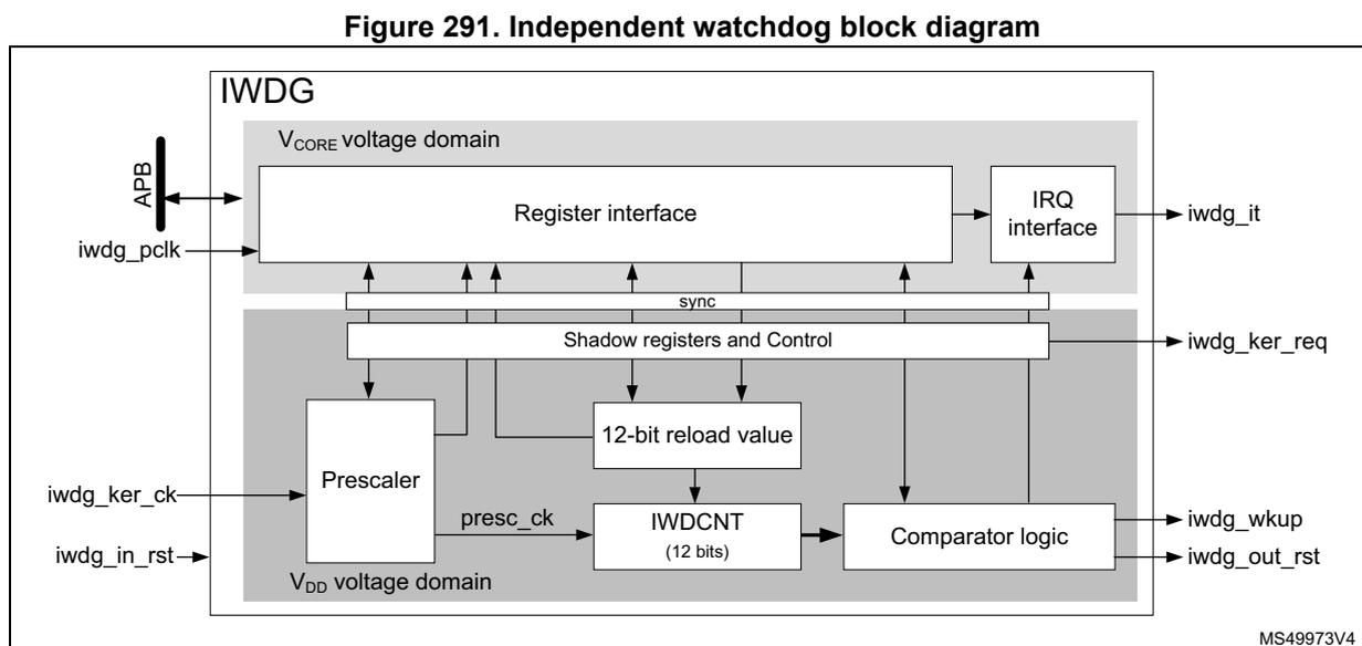
Figure 291. Independent watchdog block diagram
The register and IRQ interfaces are located into the \( V_{CORE} \) voltage domain. The watchdog function itself is located into the \( V_{DD} \) voltage domain to remain functional in low power modes. See Section 29.3 for IWDG capabilities.
The register and IRQ interfaces are mainly clocked by the APB clock (iwdg_pclk), while the watchdog function is clocked by a dedicated kernel clock (iwdg_ker_ck). A synchronization mechanism makes the data exchange between the two domains possible. Note that most of the registers located in the register interface are shadowed into the \( V_{DD} \) voltage domain.
The IWDG down-counter (IWDGCNT) is clocked by the prescaled clock (presc_ck). The prescaled clock is generated from the kernel clock iwdg_ker_ck divided by the prescaler, according to PR[3:0] bitfield.
The table below gives the timing delays according to the actions performed on the IWDG: changing the prescaler, the timeout, the window or the early wake-up comparator values or doing a refresh.
Table 162. IWDG delays versus actions (1)| TD RVU , TD PVU | TD WVU | TD EWU | TD Refresh | TD RefAuto | |||||
|---|---|---|---|---|---|---|---|---|---|
| Min | Max | Min | Max | Min | Max | Min | Max | Min | Max |
| 5 T k | 6 T k | - | 6 T k | - | 6 T k | 2 T k | 2 T k + T p | - | T p |
1. T k represents a period of the kernel clock input, T p represents a period of presc_ck.
29.4.2 IWDG internal signals
The list of IWDG internal signals is detailed in Table 163 .
Table 163. IWDG internal input/output signals
| Signal name | Signal type | Description |
|---|---|---|
| iwdg_ker_ck | Input | IWDG kernel clock |
| iwdg_ker_req | Input | IWDG kernel clock request |
| iwdg_pclk | Input | IWDG APB clock |
| iwdg_out_rst | Output | IWDG reset output |
| iwdg_in_rst | Input | IWDG reset input |
| iwdg_wkup | Output | IWDG wake-up event |
| iwdg_it | Output | IWDG early wake-up interrupt |
29.4.3 Software and hardware watchdog modes
The watchdog modes allow the application to select the way the IWDG is enabled, either by software commands (Software watchdog mode), or automatically (Hardware watchdog mode). All other functions work similarly for both Software and Hardware modes.
The Software watchdog mode is the default working mode. The independent watchdog is started by writing the value 0x0000 CCCC into the IWDG key register (IWDG_KR) , and the IWDCNT starts counting down from the reset value (0xFFFF).
In the hardware watchdog mode the independent watchdog is started automatically at power-on, or every time it is reset (via iwdg_in_rst). The IWDCNT down-counter starts counting down from the reset value 0xFFFF. The hardware watchdog mode feature is enabled through the device option bits, see Section 29.3 for details.
When the IWDG is enabled the ONF flag is set to 1.
When the IWDCNT reaches 0x0000, a reset signal is generated (iwdg_out_rst asserted).
Whenever the key value 0x0000 AAAA is written in the IWDG key register (IWDG_KR) , the IWDG_RLR value is reloaded into the IWDCNT, and the watchdog reset is prevented.
Due to re-synchronization delays, the IWDG must be refreshed before the IWDCNT down-counter reaches 1.
Once started, the IWDG can be stopped only when it is reset (iwdg_in_rst asserted).
As shown in Figure 292 , when the refresh command is executed, one period of presc_ck later, the IWDCNT is reloaded with the content of RL[11:0].
Figure 292. Reset timing due to timeout
![Figure 292. Reset timing due to timeout. This timing diagram illustrates the IWDG counter (IWDCNT) and associated signals over time. The top graph shows the IWDCNT value decreasing from 0xFFF. The counter is reloaded with RL[11:0] when a write to IWDG_KR occurs. The counter is divided into two regions: 'Refresh not allowed' (from 0xFFF down to WIN[11:0]+1) and 'Refresh allowed' (from WIN[11:0]+1 down to 1). A reset is generated (iwdg_out_rst asserted) when the counter reaches 1. The reset is cleared (iwdg_in_rst deasserted) after a period of T_presc_ck. An inset shows a detail of the IWDG_KR signal with levels 0, 1, and 2, and a T_presc_ck period.](/RM0503-STM32U0/d3b346844cbc5ff0c397918e33835e87_img.jpg)
1. If window option activated.
If the IWDG is not refreshed before the IWDCNT reaches 1, the IWDG generates a reset (iwdg_out_rst is asserted). In return, the RCC resets the IWDG (assertion of iwdg_in_rst) to clear the reset source.
29.4.4 Window option
The IWDG can also work as a window watchdog, by setting the appropriate window in the IWDG window register (IWDG_WINR) .
If the reload operation is performed while the counter is greater than WIN[11:0] + 1, a reset is generated. WIN[11:0] is located in the IWDG window register (IWDG_WINR) . As shown in Figure 293, the reset is generated one period of presc_ck after the unexpected refresh command.
The default value of the IWDG window register (IWDG_WINR) is 0x0000 0FFF, so, if not updated, the window option is disabled.
As soon as the window value changes, the down-counter (IWDCNT) is reloaded with the RL[11:0] value, to ease the estimation for where the next refresh must take place.
Figure 293. Reset timing due to refresh in the not allowed area
![Timing diagram for IWDG reset due to refresh in the not allowed area. The diagram shows the IWDGCNT value, RL[11:0], WIN[11:0] + 1, Writing 0xAAAA into IWDG_KR, iwdg_out_rst, and iwdg_in_rst signals over time. The IWDGCNT value starts at 0xFFF and decreases. The RL[11:0] value is shown as a step function. The WIN[11:0] + 1 value is shown as a step function. The Writing 0xAAAA into IWDG_KR signal is shown as a pulse. The iwdg_out_rst signal is shown as a pulse. The iwdg_in_rst signal is shown as a pulse. The Refresh not allowed area is indicated by a shaded region. The T_presc_ck period is indicated by arrows.](/RM0503-STM32U0/1ddd48a4276df97c9723366cb5359470_img.jpg)
The diagram illustrates the timing of an IWDG reset when a refresh is attempted outside the allowed window. The top graph shows the IWDGCNT value decreasing from 0xFFF. The RL[11:0] register value is shown as a step function. The WIN[11:0] + 1 value is also shown as a step function. The 'Writing 0xAAAA into IWDG_KR' signal is a pulse that occurs during the 'Refresh not allowed' period. This write operation causes the iwdg_out_rst signal to go high, which in turn causes the iwdg_in_rst signal to go low, indicating a reset. The T_presc_ck period is indicated by arrows at the bottom of the diagram. The diagram is labeled MS49975V3 in the bottom right corner.
Configuring the IWDG when the window option is enabled
- 1. Enable the IWDG by writing 0x0000 CCCC in the IWDG key register (IWDG_KR) .
- 2. Enable register access by writing 0x0000 5555 in the IWDG key register (IWDG_KR) .
- 3. Write the IWDG prescaler by programming IWDG prescaler register (IWDG_PR) .
- 4. Write the IWDG reload register (IWDG_RLR) .
- 5. If needed, enable the early wake-up interrupt, and program the early wake-up comparator, by writing the proper values into the IWDG early wake-up interrupt register (IWDG_EWCR) .
- 6. Write to the IWDG window register (IWDG_WINR) . This automatically reloads the IWDGCNT down-counter with the RL[11:0] value.
- 7. Wait for the registers to be updated (IWDG_SR = 0x0000 0000).
- 8. Write 0x0000 0000 into IWDG key register (IWDG_KR) to write-protect registers.
Note: Step 7 can be skipped if the application does not intend to disable the APB clock after the completion of this sequence.
Configuring the IWDG when the window option is disabled
When the window option it is not used, the IWDG can be configured as follows:
- 1. Enable the IWDG by writing 0x0000 CCCC in the IWDG key register (IWDG_KR) .
- 2. Enable register access by writing 0x0000 5555 in the IWDG key register (IWDG_KR) .
- 3. Write the prescaler by programming the IWDG prescaler register (IWDG_PR) .
- 4. Write the IWDG reload register (IWDG_RLR) .
- 5. If needed, enable the early wake-up interrupt, and program the early wake-up comparator, by writing the proper values into the IWDG early wake-up interrupt register (IWDG_EWCR) .
- 6. Wait for the registers to be updated ( IWDG_SR = 0x0000 0000).
- 7. Refresh the counter with RL[11:0] value, and write-protect registers by writing 0x0000 AAAA into IWDG key register (IWDG_KR) .
The figure below shows a sequence example changing the prescaler, the reload value, and then performing a refresh.
Figure 294. Changing PR, RL, and performing a refresh (1)
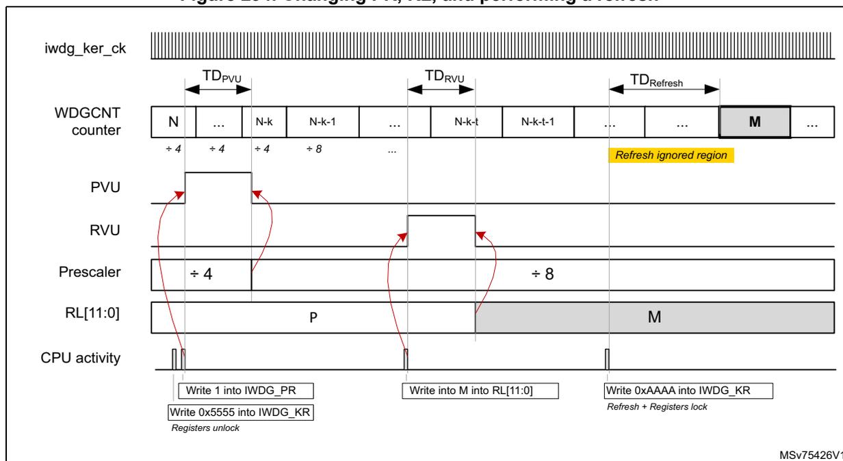
The diagram shows the following signals over time:
- iwdg_ker_ck: A continuous clock signal.
- WDGCNT counter: Shows the counter value decreasing. It starts at N, goes through N-k, N-k-1, N-k-t, N-k-t-1, and is eventually reloaded to M. Below the counter values are the division ratios: ÷ 4, ÷ 4, ÷ 4, ÷ 8, ..., and a "Refresh ignored region" highlighted in yellow before the reload to M.
- PVU (Prescaler Value Update): A status flag that goes high when a prescaler update is pending and low when complete. The duration is marked as TD PVU .
- RVU (Reload Value Update): A status flag that goes high when a reload value update is pending and low when complete. The duration is marked as TD RVU .
- Prescaler: Shows the transition from ÷ 4 to ÷ 8.
- RL[11:0]: Shows the reload value register changing from P to M.
- CPU activity:
Shows specific write operations:
- Write 1 into IWDG_PR
- Write 0x5555 into IWDG_KR (Registers unlock)
- Write M into RL[11:0]
- Write 0xAAAA into IWDG_KR (Refresh + Registers lock)
- TD Refresh : Indicates the delay for the refresh operation.
- 1. Refer to Table 162: IWDG delays versus actions for details on timing values.
Note: When the new prescaler value is accepted by the IWDG (falling edge of PVU), the new division ratio is effective when the current division sequence is completed ( N-k in the drawing).
Note: The timeout delay between the refresh (write 0xAAAA into IWDG_KR) and the watchdog reset is increased by TD Refresh .
If a refresh command is sent while the previous refresh command is not yet completed, this last refresh command is ignored.
Updating the window comparator
It is possible to update the window comparator when the IWDG is already running. The IWDGCNT is reloaded as well. The following sequence can be performed to update the window comparator:
- 1. Enable register access by writing 0x0000 5555 in the IWDG key register ( IWDG_KR ).
- 2. Write to the IWDG window register ( IWDG_WINR ). This automatically reloads the IWDGCNT down-counter with RL[11:0] value.
- 3. Wait for WVU = 0
- 4. Lock registers by writing IWDG_KR to 0x0000 0000
Step 3 can be skipped if the application does not intend to disable the APB clock after the completion of this sequence.
Figure 295 shows this sequence. As soon as the IWDG_WINR register is written, the WVU flag goes high for \( TD_{WVU} \) . After a window comparator update, a refresh is automatically performed. The refresh is effective in the worst case, on the next prescaler clock active edge after the falling edge of WVU ( \( TD_{RefAuto} \) )
Figure 295. Window comparator update (1)
![Timing diagram for window comparator update showing iwdg_ker_ck, WDGCNT counter, WVU flag, WIN[11:0], RL[11:0], and CPU activity.](/RM0503-STM32U0/702b8ccb148aa50f5194a370d92ea25c_img.jpg)
The diagram illustrates the timing sequence for updating the window comparator. The top line shows the
iwdg_ker_ck
clock signal. Below it, the
WDGCNT
counter is shown counting down from
N
to
N-k
, then it is reloaded to
M
, and continues
M-1
,
M-2
. A yellow shaded area labeled "Refresh ignored region" starts at the falling edge of the
WVU
flag and ends at the next active clock edge. The
WVU
flag goes high when
WIN[11:0]
is updated from 500 to 800 and returns low after a duration
\(
TD_{WVU}
\)
. The
WIN[11:0]
register is updated from 500 to 800. The
RL[11:0]
register holds value
M
. CPU activity shows three write operations: "Write 0x5555 into IWDG_KR" (Registers unlock), "Write 800 into IWDG_WINR", and "Write 0x0000 into IWDG_KR" (Registers lock). The timing parameters
\(
TD_{WVU}
\)
and
\(
TD_{RefAuto}
\)
are indicated.
MSv75427V1
- 1. Refer to Table 162: IWDG delays versus actions for details on timing values.
29.4.5 Debug
When the processor enters into Debug mode (core halted), the IWDGCNT down-counter either continues to work normally or stops, depending on debug capability of the product. Refer to Section 29.3 for details on the capabilities of this product.
29.4.6 Register access protection
Write accesses to IWDG prescaler register (IWDG_PR) , IWDG reload register (IWDG_RLR) , IWDG early wake-up interrupt register (IWDG_EWCR) and IWDG window register (IWDG_WINR) are protected. To modify them, first write 0x0000 5555 in the IWDG key register (IWDG_KR) . A write access to this register with a different value breaks the
sequence and register access is protected again. This is the case of the reload operation (writing 0x0000 AAAA).
A status register is available to indicate that an update of the prescaler or the down-counter reload value or the window value is ongoing.
29.5 IWDG low power modes
Depending on option bytes configuration, the IWDG can continue counting or not during the low power modes. Refer to Section 29.3 for details.
Table 164. Effect of low power modes on IWDG
| Mode | Description |
|---|---|
| Sleep | No effect. IWDG interrupts cause the device to exit from the mode. |
| Stop | The IWDG remains active or not, depending on option bytes configuration. Refer to
Section 29.3
for details. IWDG interrupts cause the device exit the Stop mode. |
| Standby | The IWDG remains active or not, depending on option bytes configuration. Refer to
Section 29.3
for details. IWDG interrupts do not make the device to exit from Standby mode. |
29.6 IWDG interrupts
The IWDG offers the possibility to generate an early interrupt depending on the value of the down-counter. The early interrupt is enabled by setting the EWIE bit of the IWDG early wake-up interrupt register (IWDG_EWCR) to 1.
A comparator value (EWIT[11:0]) allows the application to define the position where the early interrupt must be generated.
When the IWDCNT down-counter reaches the value of EWIT[11:0] - 1, the iwdg_wkup is activated, making it possible for the system to exit from low power modes, if needed.
When the APB clock is available, the iwdg_it is activated as well.
In addition, the flag EWIF of the IWDG status register (IWDG_SR) is set to 1.
The EWI interrupt is acknowledged by writing 1 to the EWIC bit in the IWDG early wake-up interrupt register (IWDG_EWCR) .
Writing into the IWDG_EWCR register also triggers a refresh of the down-counter (IWDCNT) with the reload value RL[11:0].
Figure 296. Independent watchdog interrupt timing diagram
![Figure 296. Independent watchdog interrupt timing diagram. The diagram shows the relationship between the IWDGCNT value, APB write accesses, iwdg_wkup_it signal, pclk signal, and iwdg_it signal over time. The IWDGCNT value starts at a high value and decreases linearly. A horizontal line represents the EWIT[11:0] threshold. A vertical dashed line marks the point where IWDGCNT = EWIT - 1. At this point, the iwdg_wkup_it signal goes high. A write access to the EWIC register is shown, setting EWIC to '1'. The pclk signal is shown as a series of pulses, with a shaded region indicating it is active. The iwdg_it signal goes high when the pclk is active and the iwdg_wkup_it signal is high.](/RM0503-STM32U0/f3d2ce4db7d94ca32d0ca34f64a81faf_img.jpg)
The figure is a timing diagram illustrating the Independent Watchdog (IWDG) interrupt sequence. The top graph shows the IWDGCNT value decreasing linearly over time. A horizontal line represents the EWIT[11:0] threshold. A vertical dashed line marks the point where IWDGCNT = EWIT - 1. At this point, the iwdg_wkup_it signal goes high. A write access to the EWIC register is shown, setting EWIC to '1'. The pclk signal is shown as a series of pulses, with a shaded region indicating it is active. The iwdg_it signal goes high when the pclk is active and the iwdg_wkup_it signal is high.
The early wake-up interrupt (EWI) can be used if specific safety operations or data logging must be performed before the watchdog reset is generated.
Changing the early wake-up comparator value
It is possible to change the early wake-up comparator value or to enable/disable the interrupt generation at any time, by performing the following sequence:
- 1. Enable register access by writing 0x0000 5555 in the IWDG key register (IWDG_KR) .
- 2. Enable or disable the early wake-up interrupt, and/or program the early wake-up comparator, by writing the proper values into the IWDG early wake-up interrupt register (IWDG_EWCR) .
- 3. Wait for EWU = 0, EWU is located into the IWDG status register (IWDG_SR) .
- 4. Write-protect registers by writing 0x0000 0000 to IWDG key register (IWDG_KR) .
Step 3 can be skipped if the application does not intend to disable the APB clock after the completion of this sequence.
Figure 296 shows this sequence. During the early wake-up comparator update operation the flag EWU remains to 1 for TDewu. A refresh is automatically performed. The refresh is effective on the worst case, on the next prescaler clock active edge after the falling edge of EWU (TDRefAuto).
Figure 297. Early wake-up comparator update (1)![Timing diagram for early wake-up comparator update. It shows the relationship between iwdg_ker_ck, WDGCNT counter, EWU, EWIT[11:0], RL[11:0], and CPU activity. The counter counts down from N to M, where M is the early wake-up threshold. The diagram shows that the EWIT value is updated from 500 to 300 while the counter is still counting down, and the RL value is updated to M. CPU activity is shown as a series of pulses. Timing parameters TD_EWU and TD_RefAuto are indicated. A 'Refresh ignored region' is highlighted in the counter sequence. Actions like 'Write into EWIT[11:0]', 'Write 0x5555 into IWDG_KR' (Registers unlock), and 'Write 0x0000 into IWDG_KR' (Registers lock) are shown.](/RM0503-STM32U0/b22ccb4efcb335d7e0e8b1274ebe6452_img.jpg)
1. Refer to Table 162: IWDG delays versus actions for details on timing values.
Table 165 summarizes the IWDG interrupt request.
Table 165. IWDG interrupt request
| Interrupt event | Event flag | Interrupt clear method | Interrupt enable control bit | Activated interrupt | |
|---|---|---|---|---|---|
| iwdg_it | iwdg_wkup_it | ||||
| IWDGCNT reaches EWIT value | EWIF | Writing EWIC to 1 | EWIE | γ (1) | γ (2) |
- Generated when a clock is present on iwdg_pclk input.
- Generated when a clock is present on iwdg_ker_ck input.
29.7 IWDG registers
Refer to Section 1.2 on page 51 for a list of abbreviations used in register descriptions.
The peripheral registers can be accessed by half-words (16-bit) or words (32-bit).
Most of the registers located into the register interface are shadowed into the V DD voltage domain. When the iwdg_in_rst is asserted, the watchdog logic and the shadow registers located into the V DD voltage domain are reset.
When the application reads back a watchdog register, the hardware transfers the value of the corresponding shadow register to the register interface.
When the application writes a watchdog register, the hardware updates the corresponding shadow register.
29.7.1 IWDG key register (IWDG_KR)
Address offset: 0x00
Reset value: 0x0000 0000
| 31 | 30 | 29 | 28 | 27 | 26 | 25 | 24 | 23 | 22 | 21 | 20 | 19 | 18 | 17 | 16 |
|---|---|---|---|---|---|---|---|---|---|---|---|---|---|---|---|
| Res. | Res. | Res. | Res. | Res. | Res. | Res. | Res. | Res. | Res. | Res. | Res. | Res. | Res. | Res. | Res. |
| 15 | 14 | 13 | 12 | 11 | 10 | 9 | 8 | 7 | 6 | 5 | 4 | 3 | 2 | 1 | 0 |
| KEY[15:0] | |||||||||||||||
| w | w | w | w | w | w | w | w | w | w | w | w | w | w | w | w |
Bits 31:16 Reserved, must be kept at reset value.
Bits 15:0 KEY[15:0] : Key value (write only, read 0x0000)
These bits can be used for several functions, depending upon the value written by the application:
- - 0xAAAA: reloads the RL[11:0] value into the IWDGCNT down-counter (watchdog refresh), and write-protects registers. This value must be written by software at regular intervals, otherwise the watchdog generates a reset when the counter reaches 0.
- - 0x5555: enables write-accesses to the registers.
- - 0xCCCC: enables the watchdog (except if the hardware watchdog option is selected) and write-protects registers.
- - values different from 0x5555: write-protects registers.
Note that only IWDG_PR, IWDG_RLR, IWDG_EWCR and IWDG_WINR registers have a write-protection mechanism.
29.7.2 IWDG prescaler register (IWDG_PR)
Address offset: 0x04
Reset value: 0x0000 0000
| 31 | 30 | 29 | 28 | 27 | 26 | 25 | 24 | 23 | 22 | 21 | 20 | 19 | 18 | 17 | 16 |
|---|---|---|---|---|---|---|---|---|---|---|---|---|---|---|---|
| Res. | Res. | Res. | Res. | Res. | Res. | Res. | Res. | Res. | Res. | Res. | Res. | Res. | Res. | Res. | Res. |
| 15 | 14 | 13 | 12 | 11 | 10 | 9 | 8 | 7 | 6 | 5 | 4 | 3 | 2 | 1 | 0 |
| PR[3:0] | |||||||||||||||
| Res. | Res. | Res. | Res. | Res. | Res. | Res. | Res. | Res. | Res. | Res. | Res. | rw | rw | rw | rw |
Bits 31:4 Reserved, must be kept at reset value.
Bits 3:0 PR[3:0] : Prescaler divider
These bits are write access protected, see Section 29.4.6 . They are written by software to select the prescaler divider feeding the counter clock. PVU bit of the IWDG status register (IWDG_SR) must be reset to be able to change the prescaler divider.
0000: divider / 4
0001: divider / 8
0010: divider / 16
0011: divider / 32
0100: divider / 64
0101: divider / 128
0110: divider / 256
0111: divider / 512
Others: divider / 1024
Note: Reading this register returns the prescaler value from the \( V_{DD} \) voltage domain. This value may not be up to date/valid if a write operation to this register is ongoing. For this reason the value read from this register is valid only when the PVU bit in the IWDG status register (IWDG_SR) is reset.
29.7.3 IWDG reload register (IWDG_RLR)
Address offset: 0x08
Reset value: 0x0000 0FFF
| 31 | 30 | 29 | 28 | 27 | 26 | 25 | 24 | 23 | 22 | 21 | 20 | 19 | 18 | 17 | 16 |
|---|---|---|---|---|---|---|---|---|---|---|---|---|---|---|---|
| Res. | Res. | Res. | Res. | Res. | Res. | Res. | Res. | Res. | Res. | Res. | Res. | Res. | Res. | Res. | Res. |
| 15 | 14 | 13 | 12 | 11 | |||||||||||
| Res. | Res. | Res. | Res. | RL[11:0] | |||||||||||
| rw | rw | rw | rw | rw | rw | rw | rw | rw | rw | rw | rw | ||||
Bits 31:12 Reserved, must be kept at reset value.
Bits 11:0 RL[11:0] : Watchdog counter reload value
These bits are write access protected, see Section 29.4.6 . They are written by software to define the value to be loaded in the watchdog counter each time the value 0xAAAA is written in the IWDG key register (IWDG_KR) . The watchdog counter counts down from this value. The timeout period is a function of this value and the prescaler.clock. It is not recommended to set RL[11:0] to a value lower than 2.
The RVU bit in the IWDG status register (IWDG_SR) must be reset to be able to change the reload value.
Note: Reading this register returns the reload value from the \( V_{DD} \) voltage domain. This value may not be up to date/valid if a write operation to this register is ongoing, hence the value read from this register is valid only when the RVU bit in the IWDG status register (IWDG_SR) is reset.
29.7.4 IWDG status register (IWDG_SR)
Address offset: 0x0C
Reset value: 0x0000 0000 (0xFFFF FEFF)
This register contains various status flags. Note that the mask value between parenthesis means that the reset value of ONF bit is not defined. When the IWDG is configured in
software mode, the reset value of ONF bit is 0, when the IWDG is configured in hardware mode, the reset value of ONF bit is 1.
| 31 | 30 | 29 | 28 | 27 | 26 | 25 | 24 | 23 | 22 | 21 | 20 | 19 | 18 | 17 | 16 |
|---|---|---|---|---|---|---|---|---|---|---|---|---|---|---|---|
| Res. | Res. | Res. | Res. | Res. | Res. | Res. | Res. | Res. | Res. | Res. | Res. | Res. | Res. | Res. | Res. |
| 15 | 14 | 13 | 12 | 11 | 10 | 9 | 8 | 7 | 6 | 5 | 4 | 3 | 2 | 1 | 0 |
| Res. | EWIF | Res. | Res. | Res. | Res. | Res. | ONF | Res. | Res. | Res. | Res. | EWU | WVU | RVU | PVU |
| r | r | r | r | r | r |
Bits 31:15 Reserved, must be kept at reset value.
Bit 14 EWIF : Watchdog early interrupt flag
This bit is set to '1' by hardware in order to indicate that an early interrupt is pending. This bit must be cleared by the software by writing the bit EWIC of IWDG_EWCR register to '1'.
Bits 13:9 Reserved, must be kept at reset value.
Bit 8 ONF : Watchdog enable status bit
Set to '1' by hardware as soon as the IWDG is started. In software mode, it remains to '1' until the IWDG is reset. In hardware mode, this bit is always set to '1'.
0: The IWDG is not activated
1: The IWDG is activated and needs to be refreshed regularly by the application
Bits 7:4 Reserved, must be kept at reset value.
Bit 3 EWU : Watchdog interrupt comparator value update
This bit is set by hardware to indicate that an update of the interrupt comparator value (EWIT[11:0]) or an update of the EWIE is ongoing. It is reset by hardware when the update operation is completed in the V DD voltage domain. Refer to Table 162: IWDG delays versus actions for delay values.
The EWIT[11:0] and EWIE fields can be updated only when EWU bit is reset.
Bit 2 WVU : Watchdog counter window value update
This bit is set by hardware to indicate that an update of the window value is ongoing. It is reset by hardware when the reload value update operation is completed in the V DD voltage domain. Refer to Table 162: IWDG delays versus actions for delay values.
The window value can be updated only when WVU bit is reset.
This bit is generated only if generic "window" = 1.
Bit 1 RVU : Watchdog counter reload value update
This bit is set by hardware to indicate that an update of the reload value is ongoing. It is reset by hardware when the reload value update operation is completed in the V DD voltage domain. Refer to Table 162: IWDG delays versus actions for delay values.
The reload value can be updated only when RVU bit is reset.
Bit 0 PVU : Watchdog prescaler value update
This bit is set by hardware to indicate that an update of the prescaler value is ongoing. It is reset by hardware when the prescaler update operation is completed in the V DD voltage domain. Refer to Table 162: IWDG delays versus actions for delay values.
The prescaler value can be updated only when PVU bit is reset.
Note: If several reload, prescaler, early interrupt position or window values are used by the application, it is mandatory to wait until RVU bit is reset before changing the reload value, to wait until PVU bit is reset before changing the prescaler value, to wait until WVU bit is reset before changing the window value, and to wait until EWU bit is reset before changing the
early interrupt position value. After updating the prescaler and/or the reload/window/early interrupt value, it is not necessary to wait until RVU or PVU or WVU or EWU is reset before continuing code execution, except in case of low power mode entry.
29.7.5 IWDG window register (IWDG_WINR)
Address offset: 0x10
Reset value: 0x0000 0FFF
| 31 | 30 | 29 | 28 | 27 | 26 | 25 | 24 | 23 | 22 | 21 | 20 | 19 | 18 | 17 | 16 |
|---|---|---|---|---|---|---|---|---|---|---|---|---|---|---|---|
| Res. | Res. | Res. | Res. | Res. | Res. | Res. | Res. | Res. | Res. | Res. | Res. | Res. | Res. | Res. | Res. |
| 15 | 14 | 13 | 12 | 11 | 10 | 9 | 8 | 7 | 6 | 5 | 4 | 3 | 2 | 1 | 0 |
| Res. | Res. | Res. | Res. | WIN[11:0] | |||||||||||
| rw | rw | rw | rw | rw | rw | rw | rw | rw | rw | rw | rw | ||||
Bits 31:12 Reserved, must be kept at reset value.
Bits 11:0 WIN[11:0] : Watchdog counter window value
These bits are write access protected, see Section 29.4.6 . They contain the high limit of the window value to be compared with the downcounter.
To prevent a reset, the IWDGCNT downcounter must be reloaded when its value is lower than WIN[11:0] + 1 and greater than 1.
The WVU bit in the IWDG status register (IWDG_SR) must be reset to be able to change the reload value.
Note: Reading this register returns the reload value from the V DD voltage domain. This value may not be valid if a write operation to this register is ongoing. For this reason the value read from this register is valid only when the WVU bit in the IWDG status register (IWDG_SR) is reset.
29.7.6 IWDG early wake-up interrupt register (IWDG_EWCR)
Address offset: 0x14
Reset value: 0x0000 0000
| 31 | 30 | 29 | 28 | 27 | 26 | 25 | 24 | 23 | 22 | 21 | 20 | 19 | 18 | 17 | 16 |
|---|---|---|---|---|---|---|---|---|---|---|---|---|---|---|---|
| Res. | Res. | Res. | Res. | Res. | Res. | Res. | Res. | Res. | Res. | Res. | Res. | Res. | Res. | Res. | Res. |
| 15 | 14 | 13 | 12 | 11 | 10 | 9 | 8 | 7 | 6 | 5 | 4 | 3 | 2 | 1 | 0 |
| EWIE | EWIC | Res. | Res. | EWIT[11:0] | |||||||||||
Bits 31:16 Reserved, must be kept at reset value.
Bit 15 EWIE : Watchdog early interrupt enable
Set and reset by software.
0: The early interrupt interface is disabled.
1: The early interrupt interface is enabled.
The EWU bit in the IWDG status register (IWDG_SR) must be reset to be able to change the value of this bit.
Bit 14 EWIC : Watchdog early interrupt acknowledge
The software must write a 1 into this bit in order to acknowledge the early wake-up interrupt and to clear the EWIF flag. Writing 0 has no effect, reading this flag returns a 0.
Bits 13:12 Reserved, must be kept at reset value.
Bits 11:0 EWIT[11:0] : Watchdog counter window value
These bits are write access protected (see Section 29.4.6 ). They are written by software to define at which position of the IWDGCNT down-counter the early wake-up interrupt must be generated. The early interrupt is generated when the IWDGCNT is lower or equal to EWIT[11:0] - 1.
EWIT[11:0] must be bigger than 1.
An interrupt is generated only if EWIE = 1.
The EWU bit in the IWDG status register (IWDG_SR) must be reset to be able to change the reload value.
Note: Reading this register returns the Early wake-up comparator value and the Interrupt enable bit from the \( V_{DD} \) voltage domain. This value may not be up to date/valid if a write operation to this register is ongoing, hence the value read from this register is valid only when the EWU bit in the IWDG status register (IWDG_SR) is reset.
29.7.7 IWDG register map
Table 166. IWDG register map and reset values
| Offset | Register name | 31 | 30 | 29 | 28 | 27 | 26 | 25 | 24 | 23 | 22 | 21 | 20 | 19 | 18 | 17 | 16 | 15 | 14 | 13 | 12 | 11 | 10 | 9 | 8 | 7 | 6 | 5 | 4 | 3 | 2 | 1 | 0 | |
|---|---|---|---|---|---|---|---|---|---|---|---|---|---|---|---|---|---|---|---|---|---|---|---|---|---|---|---|---|---|---|---|---|---|---|
| 0x00 | IWDG_KR | Res. | Res. | Res. | Res. | Res. | Res. | Res. | Res. | Res. | Res. | Res. | Res. | Res. | Res. | Res. | Res. | KEY[15:0] | ||||||||||||||||
| Reset value | 0 | 0 | 0 | 0 | 0 | 0 | 0 | 0 | 0 | 0 | 0 | 0 | 0 | 0 | 0 | 0 | ||||||||||||||||||
| 0x04 | IWDG_PR | Res. | Res. | Res. | Res. | Res. | Res. | Res. | Res. | Res. | Res. | Res. | Res. | Res. | Res. | Res. | Res. | Res. | Res. | Res. | Res. | Res. | Res. | Res. | Res. | Res. | Res. | Res. | Res. | Res. | Res. | PR[3:0] | ||
| Reset value | 0 | 0 | 0 | |||||||||||||||||||||||||||||||
| 0x08 | IWDG_RLR | Res. | Res. | Res. | Res. | Res. | Res. | Res. | Res. | Res. | Res. | Res. | Res. | Res. | Res. | Res. | Res. | Res. | Res. | Res. | Res. | RL[11:0] | ||||||||||||
| Reset value | 1 | 1 | 1 | 1 | 1 | 1 | 1 | 1 | 1 | 1 | 1 | |||||||||||||||||||||||
| 0x0C | IWDG_SR | Res. | Res. | Res. | Res. | Res. | Res. | Res. | Res. | Res. | Res. | Res. | Res. | Res. | Res. | Res. | Res. | Res. | EMIF | Res. | Res. | Res. | Res. | Res. | ONF | Res. | Res. | Res. | Res. | EWU | WUJ | RJU | PVU | |
| Reset value | 0 | x | 0 | 0 | 0 | 0 | ||||||||||||||||||||||||||||
| 0x10 | IWDG_WINR | Res. | Res. | Res. | Res. | Res. | Res. | Res. | Res. | Res. | Res. | Res. | Res. | Res. | Res. | Res. | Res. | Res. | Res. | Res. | Res. | WIN[11:0] | ||||||||||||
| Reset value | 1 | 1 | 1 | 1 | 1 | 1 | 1 | 1 | 1 | 1 | 1 | |||||||||||||||||||||||
| 0x14 | IWDG_EWCR | Res. | Res. | Res. | Res. | Res. | Res. | Res. | Res. | Res. | Res. | Res. | Res. | Res. | Res. | Res. | Res. | EWIE | EWIC | Res. | Res. | EWIT[11:0] | ||||||||||||
| Reset value | 0 | 0 | 0 | 0 | 0 | 0 | 0 | 0 | 0 | 0 | 0 | 0 | 0 | |||||||||||||||||||||
Refer to Section 2.2 for the register boundary addresses.