21. True random number generator (RNG)
21.1 Introduction
The RNG is a true random number generator that provides full entropy outputs to the application as 32-bit samples. It is composed of a live entropy source (analog) and an internal conditioning component.
The RNG is a NIST SP 800-90B compliant entropy source that can be used to construct a nondeterministic random bit generator (NDRBG).
The RNG true random number generator can be certified NIST SP800-90B. It can also be tested using the German BSI statistical tests of AIS-31 (T0 to T8).
21.2 RNG main features
- • The RNG delivers 32-bit true random numbers, produced by an analog entropy source conditioned by a NIST SP800-90B approved conditioning stage.
- • It can be used as the entropy source to construct a nondeterministic random bit generator (NDRBG).
- • In the NIST configuration, it produces four 32-bit random samples every 412 AHB clock cycles if \( f_{\text{AHB}} < f_{\text{threshold}} \) (256 RNG clock cycles otherwise).
- • It embeds startup and NIST SP800-90B approved continuous health tests (repetition count and adaptive proportion tests), associated with specific error management
- • It can be disabled to reduce power consumption, or enabled with an automatic low power mode (default configuration).
- • It has an AMBA ® AHB slave peripheral, accessible through 32-bit word single accesses only (else an AHB bus error is generated, and the write accesses are ignored).
21.3 RNG functional description
21.3.1 RNG block diagram
Figure 92 shows the RNG block diagram.
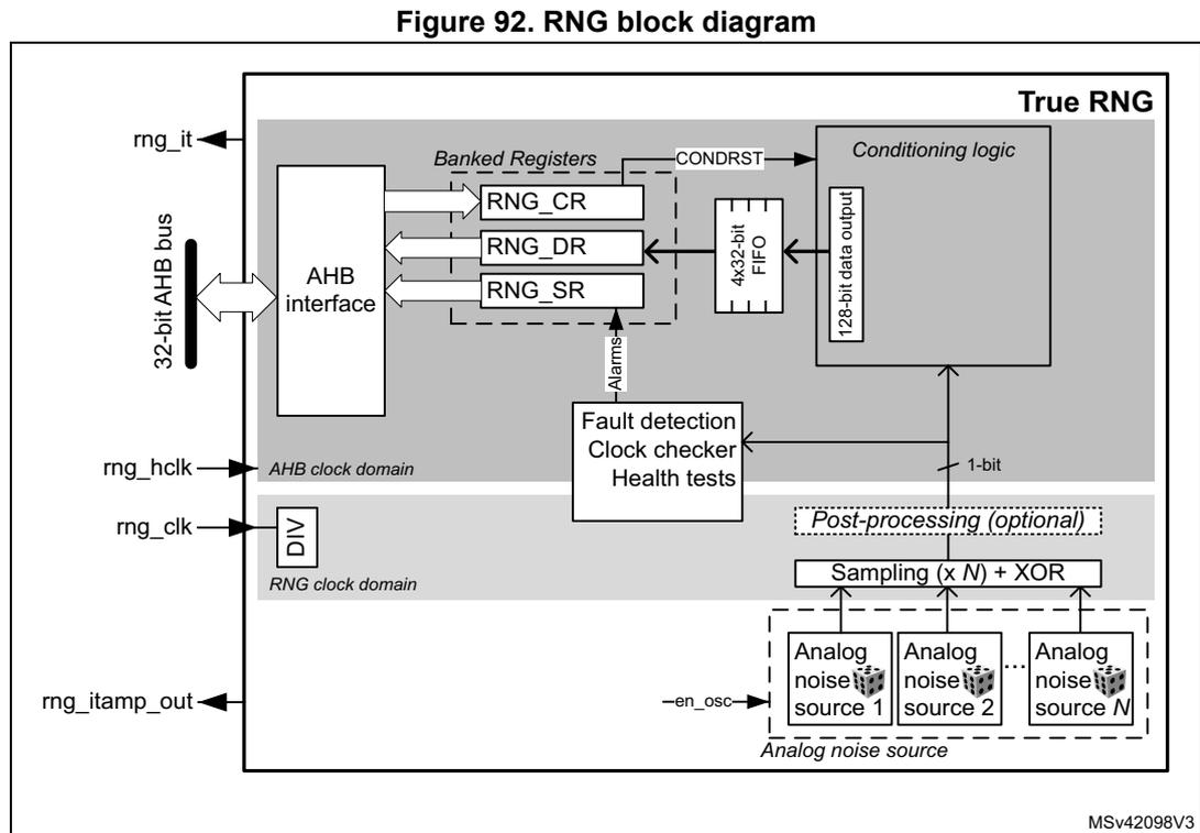
Figure 92. RNG block diagram
The diagram illustrates the internal architecture of the True Random Number Generator (RNG). It features an AHB interface connected to a 32-bit AHB bus. The interface connects to three 'Banked Registers': RNG_CR, RNG_DR, and RNG_SR. These registers are linked to a 'Conditioning logic' block via a 'CONDRST' signal. The conditioning logic outputs a '128-bit data output' which is stored in a '4x32-bit FIFO'. Below the conditioning logic is a 'Fault detection Clock checker Health tests' block, which receives 'Alarms' from the conditioning logic and provides a '1-bit' output. The RNG has two clock domains: the 'AHB clock domain' (connected to 'rng_hclk') and the 'RNG clock domain' (connected to 'rng_clk' through a 'DIV' block). External signals include 'rng_it' (interrupt), 'rng_hclk' (AHB clock), 'rng_clk' (RNG clock), and 'rng_itamp_out' (tamper event). At the bottom, 'Analog noise source' blocks (labeled 1, 2, ..., N) are connected to a 'Sampling (x N) + XOR' block, which is part of an optional 'Post-processing' stage. This stage is enabled by the '-en_osc' signal.
21.3.2 RNG internal signals
Table 112 describes a list of useful-to-know internal signals available at the RNG level, not at the STM32 product level (on pads).
Table 112. RNG internal input/output signals
| Signal name | Signal type | Description |
|---|---|---|
| rng_it | Digital output | RNG global interrupt request |
| rng_hclk | Digital input | AHB clock |
| rng_clk | Digital input | RNG dedicated clock, asynchronous to rng_hclk |
| rng_itamp_out | digital output | RNG internal tamper event signal to TAMP (XORed), triggered when an unexpected hardware fault occurs. When this signal is triggered, RNG stops delivering random samples, requiring a reset and a new initialization to be usable again. |
21.3.3 Random number generation
The true random number generator (RNG) delivers truly random data through its AHB interface at deterministic intervals.
Within its boundary RNG integrates all the required NIST components depicted on Figure 93 . Those components are an analog noise source, a digitization stage, a conditioning algorithm, a health monitoring block and two interfaces that are used to interact with the entropy source: GetEntropy and HealthTest.
Figure 93. NIST SP800-90B entropy source model
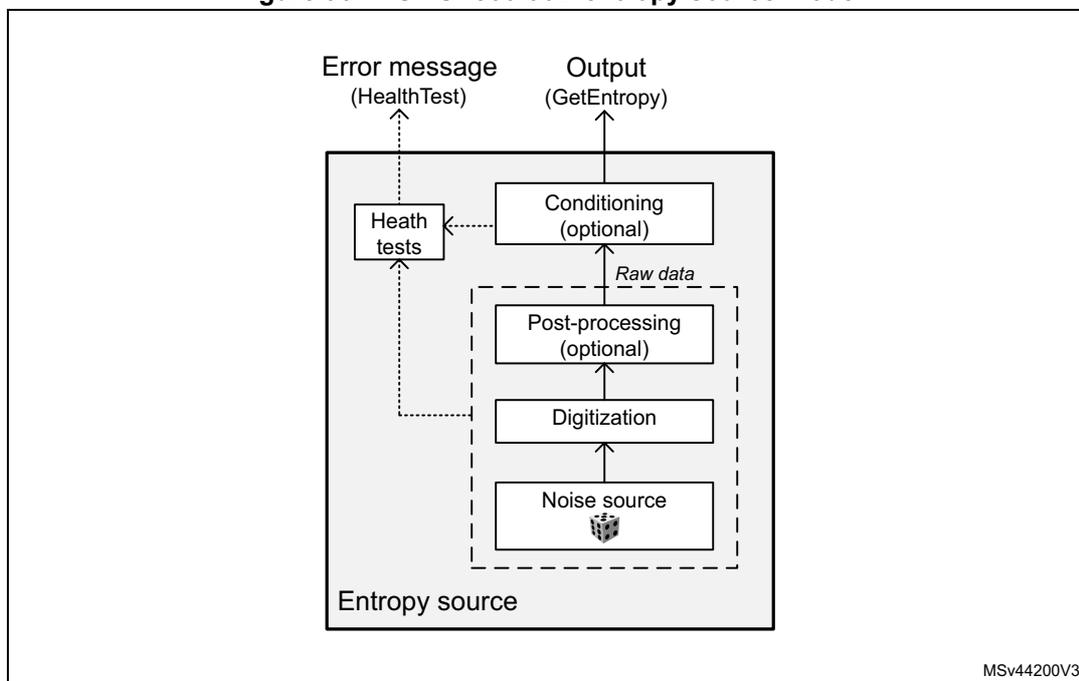
The components pictured above are detailed hereafter.
Noise source
The noise source is the component that contains the non-deterministic, entropy-providing activity that is ultimately responsible for the uncertainty associated with the bitstring output by the entropy source. This noise source provides 1-bit samples. It is composed of:
- • Multiple analog noise sources (x2), each based on three XORed free-running ring oscillator outputs. It is possible to disable those analog oscillators to save power, as described in Section 21.3.8 . Multiple oscillators are also disabled for the configuration A (see Table 115: RNG configurations ).
- • The XORing of all the noise sources into a single analog output.
- • A sampling stage of this output clocked by a dedicated clock input (rng_clk with integrated divider), delivering a 1-bit raw data output.
This noise source sampling is independent to the AHB interface clock frequency (rng_hclk), with a possibility for the software to decrease the sampling frequency by using the integrated divider.
Note: In Section 21.6 the recommended RNG clock frequencies and associated divider value are given.
Post processing
In the NIST configuration no post-processing is applied to the sampled noise source. In non-NIST configuration B (as defined in Section 21.6.2 ) a normalization debiasing is applied,
that is half of the bits are taken from the sampled noise source, half of the bits are taken from the inverted sampled noise source.
Conditioning
The conditioning component in the RNG is a deterministic function that increases the entropy rate of the resulting fixed-length bitstrings output (128-bit). The NIST SP800-90B target is full entropy on the output (128-bit).
The times required between two random number generations, and between the RNG initialization and availability of first sample are described in Section 21.5 .
Output buffer
A data output buffer can store up to four 32-bit words that have been output from the conditioning component. When four words have been read from the output FIFO through the RNG_DR register, the content of the 128-bit conditioning output register is pushed into the output FIFO, and a new conditioning round is automatically started. Four new words are added to the conditioning output register after a number of clock cycles specified in Section 21.5 .
Whenever a random number is available through the RNG_DR register, the DRDY flag changes from 0 to 1. This flag remains high until the output buffer becomes empty after reading four words from the RNG_DR register.
Note: When interrupts are enabled an interrupt is generated when this data ready flag transitions from 0 to 1. Interrupt is then cleared automatically by the RNG as explained above.
Health checks
This component ensures that the entire entropy source (with its noise source) starts then operates as expected, obtaining assurance that failures are caught quickly and with a high probability and reliability.
The RNG implements the following health check features in accordance with NIST SP800-90B. The described thresholds correspond to the value recommended for register RNG_HTCR (configuration A in Section 21.6.2 ).
- 1. Startup health tests, performed after reset and before the first use of the RNG as entropy source:
- – Repetition count test, flagging an error when the noise source has provided more than 42 consecutive bits at a constant value (0 or 1).
- – Adaptive proportion test running on a window of 1024 consecutive bits: the RNG verifies that the first bit on the outputs of the noise source is not repeated more than 711 times.
- – Known-answer tests, to verify the conditioning stage.
- 2. Continuous health tests, running indefinitely on the outputs of the noise source:
- – Repetition count test, similar to the one running in startup tests.
- – Adaptive proportion test, similar to the one running in startup tests.
- 3. Vendor specific continuous tests
- – Transition count test, flagging an error when the noise source has delivered more than 32 consecutive occurrences of 2-bit patterns (01 or 10).
- – Real-time “too slow” sampling clock detector, flagging an error when one RNG clock cycle (before divider) is smaller than AHB clock cycle divided by 32.
- 4. On-demand test of digitized noise source (raw data)
- – Supported by restarting the entropy source and rerunning the startup tests (see software reset sequence in Section 21.3.4 ). Other kinds of on-demand testing (software based) are not supported .
The CECS and SECS status bits in the RNG_SR register indicate when an error condition is detected, as detailed in Section 21.3.7 .
Note: An interrupt can be generated when an error is detected.
Above the health test thresholds are modified by changing the value in the RNG_HTCR register. See Section 21.6 for details.
21.3.4 RNG initialization
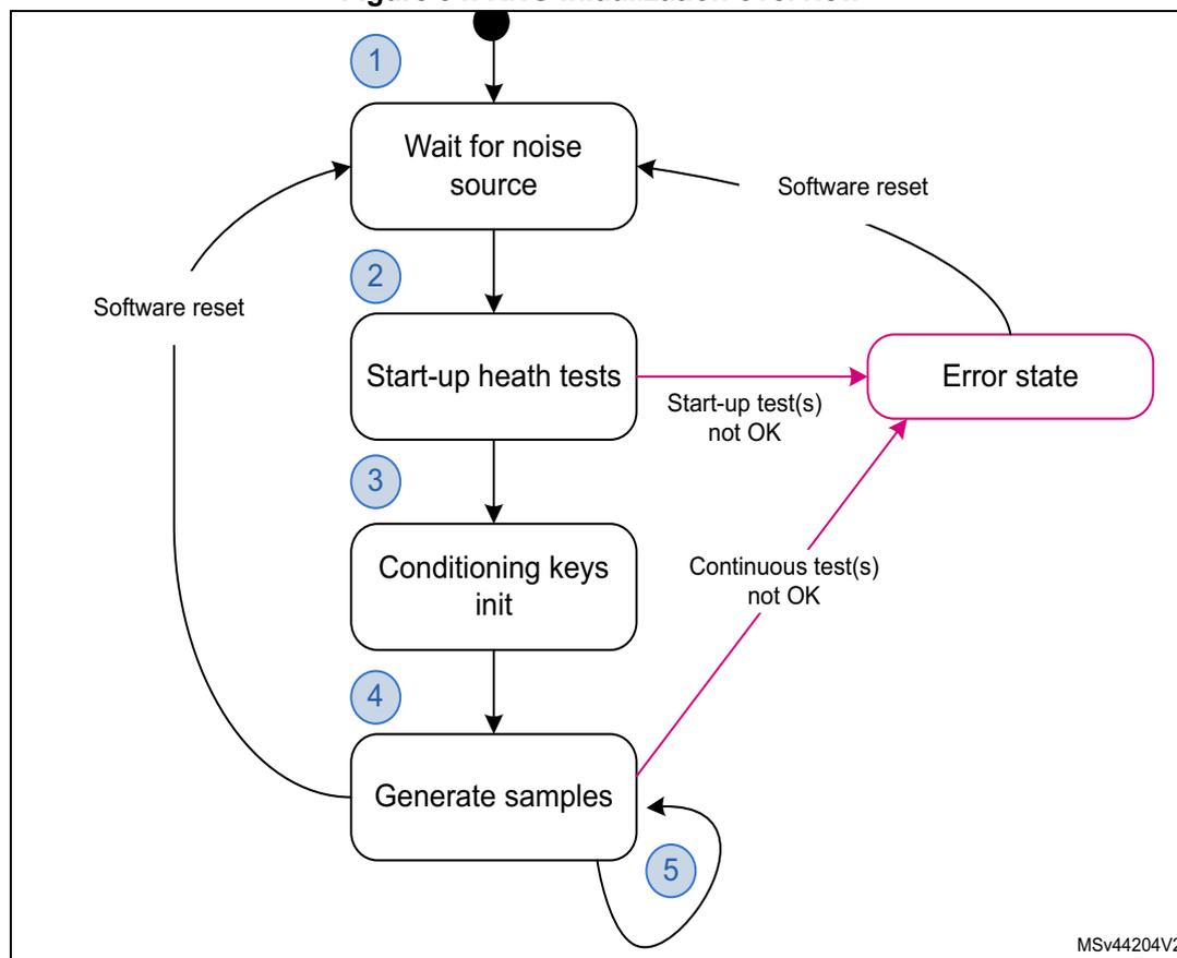
The RNG simplified state machine is pictured on Figure 94 .
After enabling the RNG (RNGEN = 1 in RNG_CR), the following chain of events occurs:
- 1. The analog noise source is enabled, and by default the RNG waits 16 cycles of RNG clock cycles (before divider) before starting to sample the analog output and filling the 128-bit conditioning shift register.
- 2. The conditioning hardware initializes, automatically triggering startup behavior test on the raw data samples and known-answer tests.
- 3. When startup health tests are completed. During this time, three 128-bit noise source samples are used.
- 4. The conditioning stage internal input data buffer is filled again with 128-bit and a number of conditioning rounds defined by the RNG configuration (NIST or non-NIST) is performed. The output buffer is then filled with the post processing result.
- 5. The output buffer is refilled automatically according to the RNG usage.
The associated initialization time can be found in Section 21.5 .
Figure 94. RNG initialization overview
graph TD
    Start(( )) --> Step1[1: Wait for noise source]
    Step1 --> Step2[2: Start-up health tests]
    Step2 --> Step3[3: Conditioning keys init]
    Step3 --> Step4[4: Generate samples]
    Step4 --> Step5((5))
    Step5 --> Step1
    Step2 -- "Start-up test(s) not OK" --> Error[Error state]
    Step4 -- "Continuous test(s) not OK" --> Error
    Error -- "Software reset" --> Step1
    Step4 -- "Software reset" --> Step1
Figure 94 also highlights a possible software reset sequence, implemented by:
- 1. Writing bits
RNGEN = 0andCONDRST = 1in theRNG_CRregister with the same RNG configuration and a newCLKDIVif needed. - 2. Then writing
RNGEN = 1andCONDRST = 0in theRNG_CRregister. - 3. Wait for random number to be ready, after initialization completes.
Note: When the RNG peripheral is reset through RCC (hardware reset), the RNG configuration for optimal randomness is lost in the RNG registers. Software reset with
CONFIGLOCK
set preserves the RNG configuration.
21.3.5 RNG operation
Normal operation
To run the RNG using interrupts, the following steps are recommended:
- 1. Check
Section 21.6
to verify if a specific RNG configuration is required for the application.
- – In this case, write in the
RNG_CRregister the bitCONDRST = 1together with the correct RNG configuration. Then perform a second write to theRNG_CRregister
- – In this case, write in the
with the bit CONDRST = 0, the interrupt enable bit IE = 1 and the RNG enable bit RNGEN = 1.
- – If it is not the case perform a write to the RNG_CR register with the interrupt enable bit IE = 1 and the RNG enable bit RNGEN = 1.
- 2. An interrupt is now generated when a random number is ready or when an error occurs. Therefore, at each interrupt, check that:
- – No error occurred. The SEIS and CEIS bits must be set to 0 in the RNG_SR register.
- – A random number is ready. The DRDY bit must be set to 1 in the RNG_SR register.
- – If the above two conditions are true the content of the RNG_DR register can be read up to four consecutive times. If valid data is available in the conditioning output buffer, four additional words can be read by the application (in this case the DRDY bit is still high). If one or both of the above conditions are false, the RNG_DR register must not be read. If an error occurred, the error recovery sequence described in Section 21.3.7 must be used.
- 2. An interrupt is now generated when a random number is ready or when an error occurs. Therefore, at each interrupt, check that:
To run the RNG in polling mode following steps are recommended:
- 1. Check
Section 21.6
to verify if a specific RNG configuration is required for the application.
- – If it is the case write in the RNG_CR register the bit CONDRST = 1 together with the correction RNG configuration. Then perform a second write to the RNG_CR register with the bit CONDRST = 0 and the RNG enable bit RNGEN = 1.
- – If it is not the case only enable the RNG by setting the RNGEN bit to 1 in the RNG_CR register.
- 2. Read the RNG_SR register and check that:
- – No error occurred (the SEIS and CEIS bits must be set to 0)
- – A random number is ready (the DRDY bit must be set to 1)
- 3. If above conditions are true read the content of the RNG_DR register up to four consecutive times. If valid data is available in the conditioning output buffer four additional words can be read by the application (in this case the DRDY bit is still high). If one or both of the above conditions are false, the RNG_DR register must not be read. If an error occurred, the error recovery sequence described in Section 21.3.7 must be used.
Note:
When data is not ready (DRDY = 0) RNG_DR returns zero.
It is recommended to always verify that RNG_DR is different from zero. Because when it is the case a seed error occurred between RNG_SR polling and RND_DR output reading (rare event).
If the random number generation period is a concern to the application and if NIST compliance is not required it is possible to select a faster RNG configuration by using the RNG configuration “B”, described in Section 21.6 . The gain in random number generation speed is summarized in Section 21.5 .
Low-power operation
If the power consumption is a concern to the application, low-power strategies can be used, as described in Section 21.3.8 .
Software post-processing
No specific software post-processing/conditioning is expected to meet the AIS-31 or NIST SP800-90B approvals.
Built-in health check functions are described in Section 21.3.3: Random number generation .
21.3.6 RNG clocking
The RNG runs on two different clocks: the AHB bus clock and a dedicated RNG clock.
The AHB clock is used to clock the AHB banked registers and conditioning component. The RNG clock, coupled with a programmable divider (see CLKDIV bitfield in the RNG_CR register) is used for noise source sampling. Recommended clock configurations are detailed in Section 21.6: RNG entropy source validation .
Note: When the CED bit in the RNG_CR register is set to 0, the RNG clock frequency before the internal divider must be higher than the AHB clock frequency divided by 32, otherwise the clock checker always flags a clock error (CECS = 1 in the RNG_SR register).
See Section 21.3.1: RNG block diagram for details (AHB and RNG clock domains).
21.3.7 Error management
In parallel to random number generation a health check block verifies the correct noise source behavior and the frequency of the RNG source clock as detailed in this section. Associated error state is also described.
Clock error detection
When the clock error detection is enabled (CED = 0) and if the RNG clock frequency is too low, the RNG sets to 1 both the CEIS and CECS bits to indicate that a clock error occurred. In this case, the application must check that the RNG clock is configured correctly (see Section 21.3.6: RNG clocking ) and then it must clear the CEIS bit interrupt flag. The CECS bit is automatically cleared when the clocking condition is normal.
Note: The clock error has no impact on generated random numbers that is the application can still read the RNG_DR register.
CEIS is set only when CECS is set to 1 by RNG.
Noise source error detection
When a noise source (or seed) error occurs, the RNG stops generating random numbers and sets to 1 both SEIS and SECS bits to indicate that a seed error occurred. If a value is available in the RNG_DR register, it must not be used as it may not have enough entropy.
When ARDIS is cleared (auto-reset enabled) clear the SEIS interrupt status bit in the RNG_SR register before drawing random numbers again.
When ARDIS is set (auto-reset disabled) the following sequence must be used to fully recover from a seed error:
- 1. Write CONDRST at 1 and at 0 in the RNG_CR register to reset the conditioning logic.
- 2. Wait for the CONDRST bit to be cleared by hardware. Then clear the SEIS interrupt status bit in the RNG_SR register.
- 3. If SECS is still set in RNG_SR it means a new seed error occurred (unlikely). In this case go back to step 1).
Note: After a seed error RNG restarts generating random numbers when SECS is cleared. When the application sets the ARDIS bit in the RNG_CR register, the auto-reset is disabled. CONDRST must be used in step 1.
RNG tamper errors
When an unexpected error is found by the RNG an internal tamper event is triggered in the TAMP peripheral, and the RNG stops delivering random data.
When this event occurs, the secure application needs to reset the RNG peripheral either using the central reset management or the global SoC reset. Then a proper initialization of the RNG is required, again.
21.3.8 RNG low-power use
If power consumption is a concern, the RNG can be disabled as soon as the DRDY bit is set to 1 by setting the RNGEN bit to 0 in the RNG_CR register. As the post-processing logic and the output buffer remain operational while RNGEN = 0 following features are available to the software:
- • If there are valid words in the output buffer four random numbers can still be read from the RNG_DR register.
- • If there are valid bits in the conditioning output internal register four additional random numbers can be still be read from the RNG_DR register. If it is not the case RNG must be reenabled by the application until the expected new noise source bits threshold is reached (128-bit in NIST mode) and a complete conditioning round is done.
Four new random words are then available only if the expected number of conditioning round is reached (two if NISTC = 0). The overall time can be found in Section 21.5: RNG processing time on page 496 .
When disabling the RNG the user deactivates all the analog seed generators, whose power consumption is given in the datasheet electrical characteristics section. The user also gates all the logic clocked by the RNG clock. Note that this strategy is adding latency before a random sample is available on the RNG_DR register, because of the RNG initialization time.
If the RNG block is disabled during initialization (that is well before the DRDY bit rises for the first time), the initialization sequence resumes from where it was stopped when RNGEN bit is set to 1, unless the application resets the conditioning logic using CONDRST bit in the RNG_CR register.
When the application wants to disable the RNG clock it is recommended to wait two RNG kernel clock cycles between clearing the RNGEN bit and disabling the RNG kernel clock using the RCC.
Also, when application needs to enter a power mode where RNG is de-activated, it is recommended to wait two RNG kernel clock cycles between clearing the RNGEN bit and entering the low power mode using the PWR.
In the two cases above, to avoid unexpected consumption when RNG analog oscillators stay active, application can set the bit 13 in RNG_CR register. Setting this bit adds some marginal power consumption while RNGEN bit is set (RNG activated).
Note: The power modes where RNG is deactivated (that is retained or not available) can be found in the PWR section.
21.4 RNG interrupts
In the RNG an interrupt can be produced on the following events:
- • Data ready flag
- • Seed error, see Section 21.3.7: Error management
- • Clock error, see Section 21.3.7: Error management
Dedicated interrupt enable control bits are available as shown in Table 113 .
Table 113. RNG interrupt requests
| Interrupt acronym | Interrupt event | Event flag | Enable control bit | Interrupt clear method |
|---|---|---|---|---|
| RNG | Data ready flag | DRDY | IE | None (automatic) |
| Seed error flag | SEIS | IE | Write CONDRST to 1 then to 0 unless ARDIS is cleared (see
Section 21.3.7
). Write 0 to SEIS. | |
| Clock error flag | CEIS | IE | Write 0 to CEIS |
The user can enable or disable the above interrupt sources individually by changing the mask bits or the general interrupt control bit IE in the RNG_CR register. The status of the individual interrupt sources can be read from the RNG_SR register.
Note: Interrupts are generated only when RNG is enabled.
21.5 RNG processing time
In recommended configuration A or C described in Table 115 , the time between two sets of four 32-bit data is either:
- • 203 x N AHB cycles if \( f_{\text{AHB}} < f_{\text{threshold}} \) (conditioning stage is limiting), or
- • 128 x N RNG cycles \( f_{\text{AHB}} \geq f_{\text{threshold}} \) (noise source stage is limiting).
With \( f_{\text{threshold}} = 1.6 \times f_{\text{RNG}} \) , for instance 77 MHz if \( f_{\text{RNG}} = 48 \) MHz. Value N is defined in Section 21.6: RNG entropy source validation .
Note: When CLKDIV is different from zero, \( f_{\text{RNG}} \) must take into account the internal divider ratio.
If configuration B is selected the performance figures become:
- • 203 AHB cycles if \( f_{\text{AHB}} < f_{\text{threshold}} \) or
- • 32 RNG cycles \( f_{\text{AHB}} \geq f_{\text{threshold}} \)
with \( f_{\text{threshold}} = 6.5 \times f_{\text{RNG}} \) .
Initialization time
More time is needed for the first set of random numbers after the device exits reset (see Section 1.3.4: RNG initialization ). Table below gives details on how to compute the time spent in each initialization step.
Table 114. RNG initialization times
| Initialization step | Configuration A or C, reset value | Configuration B |
|---|---|---|
| Wait for noise source, then startup health tests | Max((wait_noise (1) + 11 + 1024 x CLKDIV) RNG_cycles, 13 x 203 AHB_cycles) | Max(16 + 1035 RNG_cycles, 13 x 203 AHB_cycles) |
| Conditioning keys initialization | Max((1+2xN) x 128 x CLKDIV) RNG_cycles + 203 AHB_cycles, (128 x CLKDIV) RNG_cycles + (2xN+2) x 203 AHB_cycles) | Max (3 x 32 RNG_cycles + 203 AHB_cycles, 32 RNG_cycles + 4 x 203 AHB_cycles) |
1. 192 RNG_cycles (configuration A or C), 16 RNG_cycles (reset value)
As an example, if AHB clock= 54 MHz and RNG clock= 48 MHz then the initialization time is around 79 µs in the configuration C (CLKDIV=1, N=2) and 66 µs in the configuration B.
21.6 RNG entropy source validation
21.6.1 Introduction
In order to assess the amount of entropy available from the RNG, STMicroelectronics has tested the peripheral using the German BSI AIS-31 statistical tests (T0 to T8), and NIST SP800-90B test suite.
21.6.2 Validation conditions
STMicroelectronics has tested the RNG true random number generator in the following conditions:
- • RNG clock rng_clk = 48 MHz
- • RNG configurations are described in Table 115 . Note that only configuration A can be certified NIST SP800-90B. Refer to Table 116 to select the best configuration for the application.
- • Configuration C can be used when configuration A is not flagged as certified.
Table 115. RNG configurations
| Configuration | RNG_CR bits | Loop number (N) | RNG_HTCR register | RNG_NSCR register | |||||
|---|---|---|---|---|---|---|---|---|---|
| NISTC bit | RNG_CONFIG1 [5:0] | CLKDIV [3:0] | RNG_CONFIG2 [2:0] (1) | RNG_CONFIG3 [3:0] (2) | CED bit | ||||
| A | Refer to NIST compliant RNG configuration table in AN4230 available from www.st.com . This application note also indicates if this configuration is part of an existing NIST SP800-90B Entropy Certificate listed on https://csrc.nist.gov/projects/cryptographic-module-validation-program . | ||||||||
| B | 1 | 0x18 | 0x0 (3) | 0x0 | 0x0 | 0 | 1 | 0x0000 AAC7 (4) | default |
| C | 0 | 0x0F | 0x0 | 0xD | 0 | 2 | default | ||
1. 0x1 value is recommended instead of 0x0 for RNG_CONFIG2[2:0], when RNG power consumption is critical. See the end of Section 21.3.8 for details.
2. RNG_CONFIG3[1:0] defines the loop number N: 0x0 corresponds to N=1, 0x1 to N=2, 0x2 to N=3, 0x3 to N=4
- 3. The noise source sampling must be 48 MHz or less. Hence, if the RNG clock is different from 48 MHz, this value of CLKDIV must be adapted. See the CLKDIV bitfield description in Section 21.7.1 for details.
- 4. This value can be fixed in the RNG driver (it does not depend upon the STM32 product).
Table 116. Configuration selection
| Section criteria | Config A | Config B | Config C |
|---|---|---|---|
| Suitable to generate NIST compliant cryptographic keys | Yes | No | |
| Entropy (1) | Certified | Good | Very good |
| Speed (2) | Baseline | Faster | Baseline |
- 1. For configurations B and C entropy is verified using AIS-31 test suite (T0 to T8).
- 2. When speed is not enough for application a NIST compliant DRBG can be used to increase throughput.
For details on data collection and the running of statistical test suites refer to AN4230 “ STM32 microcontrollers random number generation validation using NIST statistical test suite ” available from www.st.com .
21.7 RNG registers
The RNG is associated with a control register, a data register and a status register.
21.7.1 RNG control register (RNG_CR)
Address offset: 0x000
Reset value: 0x0080 0D00
| 31 | 30 | 29 | 28 | 27 | 26 | 25 | 24 | 23 | 22 | 21 | 20 | 19 | 18 | 17 | 16 |
|---|---|---|---|---|---|---|---|---|---|---|---|---|---|---|---|
| CONFIGLOCK | COND_RST | Res. | Res. | Res. | Res. | RNG_CONFIG1[5:0] | CLKDIV[3:0] | ||||||||
| rs | rw | rw | rw | rw | rw | rw | rw | rw | rw | rw | rw | ||||
| 15 | 14 | 13 | 12 | 11 | 10 | 9 | 8 | 7 | 6 | 5 | 4 | 3 | 2 | 1 | 0 |
| RNG_CONFIG2[2:0] | NISTC | RNG_CONFIG3[3:0] | ARDIS | Res. | CED | Res. | IE | RNGEN | Res. | Res. | |||||
| rw | rw | rw | rw | rw | rw | rw | rw | rw | rw | rw | rw | ||||
Bit 31 CONFIGLOCK : RNG Config lock
0: Writes to the RNG_NSCR, RNG_HTCR and RNG_CR configuration bits [29:4] are allowed.
1: Writes to the RNG_NSCR, RNG_HTCR and RNG_CR configuration bits [29:4] are ignored until the next RNG reset.
Once set, this bit can only be cleared when RNG is reset (set once bit).
Bit 30 CONDRST : Conditioning soft reset
Write 1 and then write 0 to reset the conditioning logic, clear all the FIFOs and start a new RNG initialization process, with RNG_SR cleared. Registers RNG_CR, RNG_NSCR and RNG_HTCR are not changed by CONDRST.
This bit must be set to 1 in the same access that set any configuration bits [29:4]. In other words, when CONDRST bit is set to 1 correct configuration in bits [29:4] must also be written.
When CONDRST is set to 0 by the software, its value goes to 0 when the reset process is done. It takes about 2 AHB clock cycles + 2 RNG clock cycles.
Bits 29:26 Reserved, must be kept at reset value.
Bits 25:20 RNG_CONFIG1[5:0] : RNG configuration 1
Reserved to the RNG configuration (bitfield 1). Must be initialized using the recommended value documented in Section 21.6: RNG entropy source validation .
Writing any bit of RNG_CONFIG1 is taken into account only if the CONDRST bit is set to 1 in the same access, while CONFIGLOCK remains at 0. Writing to this bit is ignored if CONFIGLOCK = 1.
Bits 19:16 CLKDIV[3:0] : Clock divider factor
This value used to configure an internal programmable divider (from 1 to 16) acting on the incoming RNG clock. These bits can be written only when the core is disabled (RNGEN = 0).
0x0: internal RNG clock after divider is similar to incoming RNG clock.
0x1: two RNG clock cycles per internal RNG clock.
0x2: \( 2^2 \) (= 4) RNG clock cycles per internal RNG clock.
...
0xF: \( 2^{15} \) RNG clock cycles per internal clock (for example, an incoming 48 MHz RNG clock becomes a 1.5 kHz internal RNG clock)
Writing these bits is taken into account only if the CONDRST bit is set to 1 in the same access, while CONFIGLOCK remains at 0. Writing to this bit is ignored if CONFIGLOCK = 1.
Bits 15:13 RNG_CONFIG2[2:0] : RNG configuration 2
Reserved to the RNG configuration (bitfield 2). Bit 13 can be set when RNG power consumption is critical. See Section 21.3.8: RNG low-power use . Refer to the RNG_CONFIG1 bitfield for details.
Bit 12 NISTC : NIST custom
0: Hardware default values for NIST compliant RNG. In this configuration per 128-bit output two conditioning loops are performed and 256 bits of noise source are used.
1: Custom values for NIST compliant RNG. See Section 21.6: RNG entropy source validation for recommended configuration.
Writing this bit is taken into account only if CONDRST bit is set to 1 in the same access, while CONFIGLOCK remains at 0. Writing to this bit is ignored if CONFIGLOCK = 1.
Bits 11:8 RNG_CONFIG3[3:0] : RNG configuration 3
Reserved to the RNG configuration (bitfield 3). Refer to RNG_CONFIG1 bitfield for details. If the NISTC bit is cleared in this register RNG_CONFIG3 bitfield values are ignored by RNG.
Bit 7 ARDIS : Auto reset disable
Set this bit to deactivate the auto-reset feature.
0: Auto-reset enabled
1: Auto-reset disabled
Keeping the auto-reset enabled (automatic clearance of the SECS bit) simplifies the management of noise source errors, as described in Section 21.3.7: Error management .
Writing this bit is taken into account only if CONDRST bit is set to 1 in the same access, while CONFIGLOCK remains at 0. Writing to this bit is ignored if CONFIGLOCK = 1.
Bit 6 Reserved, must be kept at reset value.
Bit 5 CED : Clock error detection
0: Clock error detection enabled
1: Clock error detection is disabled
The clock error detection cannot be enabled nor disabled on-the-fly when the RNG is enabled, that is to enable or disable CED, the RNG must be disabled.
Writing this bit is taken into account only if the CONDRST bit is set to 1 in the same access, while CONFIGLOCK remains at 0. Writing to this bit is ignored if CONFIGLOCK = 1.
Bit 4 Reserved, must be kept at reset value.
Bit 3 IE : Interrupt enable
0: RNG interrupt is disabled
1: RNG interrupt is enabled. An interrupt is pending as soon as the DRDY, SEIS, or CEIS is set in the RNG_SR register.
Bit 2 RNGEN : True random number generator enable
0: True random number generator is disabled. Analog noise sources are powered off and logic clocked by the RNG clock is gated.
1: True random number generator is enabled.
Bits 1:0 Reserved, must be kept at reset value.
21.7.2 RNG status register (RNG_SR)
Address offset: 0x004
Reset value: 0x0000 0000
| 31 | 30 | 29 | 28 | 27 | 26 | 25 | 24 | 23 | 22 | 21 | 20 | 19 | 18 | 17 | 16 |
|---|---|---|---|---|---|---|---|---|---|---|---|---|---|---|---|
| Res. | Res. | Res. | Res. | Res. | Res. | Res. | Res. | Res. | Res. | Res. | Res. | Res. | Res. | Res. | Res. |
| 15 | 14 | 13 | 12 | 11 | 10 | 9 | 8 | 7 | 6 | 5 | 4 | 3 | 2 | 1 | 0 |
| Res. | Res. | Res. | Res. | Res. | Res. | Res. | Res. | Res. | SEIS | CEIS | Res. | Res. | SECS | CECS | DRDY |
| rc_w0 | rc_w0 | r | r | r |
Bits 31:7 Reserved, must be kept at reset value.
Bit 6 SEIS : Seed error interrupt status
This bit is set at the same time as SECS. It is cleared by writing 0 (unless CONDRST is used). Writing 1 has no effect.
0: No faulty sequence detected
1: At least one faulty sequence is detected. See SECS bit description for details.
An interrupt is pending if IE = 1 in the RNG_CR register.
Bit 5 CEIS : Clock error interrupt status
This bit is set at the same time as CECS. It is cleared by writing 0. Writing 1 has no effect.
0: The RNG clock is correct ( \( f_{\text{RNGCLK}} > f_{\text{HCLK}}/32 \) )
1: The RNG clock before the internal divider is detected too slow ( \( f_{\text{RNGCLK}} < f_{\text{HCLK}}/32 \) )
An interrupt is pending if IE = 1 in the RNG_CR register.
Bits 4:3 Reserved, must be kept at reset value.
Bit 2 SECS : Seed error current status
0: No faulty sequence has currently been detected. If the SEIS bit is set, this means that a faulty sequence was detected and the situation has been recovered.
1: At least one of the following faulty sequences has been detected:
- – Runtime repetition count test failed (noise source has provided more than 24 consecutive bits at a constant value 0 or 1, or more than 32 consecutive occurrence of two bits patterns 01 or 10)
- – Startup or continuous adaptive proportion test on noise source failed.
- – Startup post-processing/conditioning sanity check failed.
Bit 1 CECS : Clock error current status
0: The RNG clock is correct ( \( f_{\text{RNGCLK}} > f_{\text{HCLK}}/32 \) ). If the CEIS bit is set, this means that a slow clock was detected and the situation has been recovered.
1: The RNG clock is too slow ( \( f_{\text{RNGCLK}} < f_{\text{HCLK}}/32 \) ).
Note: CECS bit is valid only if the CED bit in the RNG_CR register is set to 0.
Bit 0 DRDY : Data ready
0: The RNG_DR register is not yet valid, no random data is available.
1: The RNG_DR register contains valid random data.
Once the output buffer becomes empty (after reading the RNG_DR register), this bit returns to 0 until a new random value is generated.
Note: The DRDY bit can rise when the peripheral is disabled (RNGEN = 0 in the RNG_CR register).
If IE=1 in the RNG_CR register, an interrupt is generated when DRDY = 1.
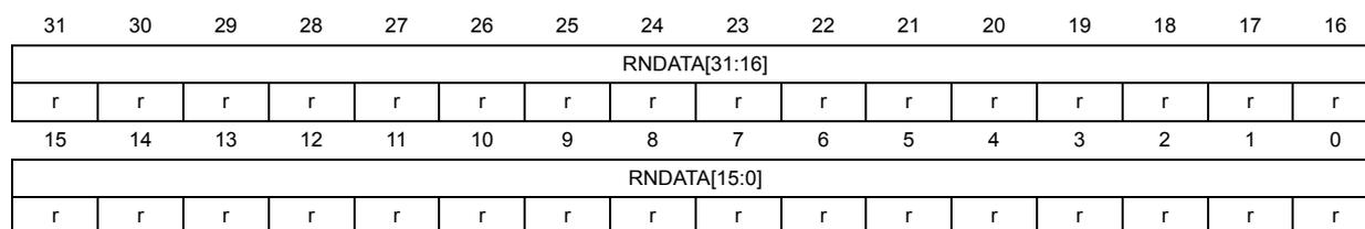
21.7.3 RNG data register (RNG_DR)
Address offset: 0x008
Reset value: 0x0000 0000
The RNG_DR register is a read-only register that delivers a 32-bit random value when read. The content of this register is valid when the DRDY = 1 and the value is not 0x0, even if RNGEN = 0.
| 31 | 30 | 29 | 28 | 27 | 26 | 25 | 24 | 23 | 22 | 21 | 20 | 19 | 18 | 17 | 16 |
| RNDATA[31:16] | |||||||||||||||
| r | r | r | r | r | r | r | r | r | r | r | r | r | r | r | r |
| 15 | 14 | 13 | 12 | 11 | 10 | 9 | 8 | 7 | 6 | 5 | 4 | 3 | 2 | 1 | 0 |
| RNDATA[15:0] | |||||||||||||||
| r | r | r | r | r | r | r | r | r | r | r | r | r | r | r | r |
Bits 31:0 RNDATA[31:0] : Random data
32-bit random data, which are valid when DRDY = 1. When DRDY = 0, the RNDATA value is zero.
When DRDY is set, it is recommended to always verify that RNG_DR is different from zero. The zero value means that a seed error occurred between RNG_SR polling and RND_DR output reading (a rare event).
21.7.4 RNG noise source control register (RNG_NSCR)
Address offset: 0x00C
Reset value: 0x0000 003F
Writing in RNG_NSCR is taken into account only if the CONDRST bit is set, and the CONFIGLOCK bit is cleared in RNG_CR. Writing to this register is ignored if CONFIGLOCK= 1.
| 31 | 30 | 29 | 28 | 27 | 26 | 25 | 24 | 23 | 22 | 21 | 20 | 19 | 18 | 17 | 16 |
|---|---|---|---|---|---|---|---|---|---|---|---|---|---|---|---|
| Res. | Res. | Res. | Res. | Res. | Res. | Res. | Res. | Res. | Res. | Res. | Res. | Res. | Res. | Res. | Res. |
| 15 | 14 | 13 | 12 | 11 | 10 | 9 | 8 | 7 | 6 | 5 | 4 | 3 | 2 | 1 | 0 |
| Res. | Res. | Res. | Res. | Res. | Res. | Res. | Res. | Res. | Res. | EN_OSC2[2:0] | EN_OSC1[2:0] | ||||
| rw | rw | rw | rw | rw | rw | ||||||||||
Bits 31:6 Reserved, must be kept at reset value.
Bits 5:3 EN_OSC2[2:0] :
When the RNG is enabled (RNGEN bit set), each bit of this bitfield enables one of the three inputs from the oscillator instance number 2. The bitfield has no effect otherwise.
Bits 2:0 EN_OSC1[2:0] :
When the RNG is enabled (RNGEN bit set), each bit of this bitfield enables one of the three inputs from the oscillator instance number 1. The bitfield has no effect otherwise.
21.7.5 RNG health test control register (RNG_HTCR)
Address offset: 0x010
Reset value: 0x0000 72AC
Writing in RNG_HTCR is taken into account only if the CONDRST bit is set, and the CONFIGLOCK bit is cleared in the RNG_CR. Writing to this register is ignored if CONFIGLOCK=1.
| 31 | 30 | 29 | 28 | 27 | 26 | 25 | 24 | 23 | 22 | 21 | 20 | 19 | 18 | 17 | 16 |
|---|---|---|---|---|---|---|---|---|---|---|---|---|---|---|---|
| HTCFG[31:16] | |||||||||||||||
| rw | rw | rw | rw | rw | rw | rw | rw | rw | rw | rw | rw | rw | rw | rw | rw |
| 15 | 14 | 13 | 12 | 11 | 10 | 9 | 8 | 7 | 6 | 5 | 4 | 3 | 2 | 1 | 0 |
| HTCFG[15:0] | |||||||||||||||
| rw | rw | rw | rw | rw | rw | rw | rw | rw | rw | rw | rw | rw | rw | rw | rw |
Bits 31:0 HTCFG[31:0] : health test configuration
This configuration is used by RNG to configure the health tests. See Section 21.6: RNG entropy source validation for the recommended value.
Note: The RNG behavior, including the read to this register, is not guaranteed if a different value from the recommended value is written.
21.7.6 RNG register map
Table 117. RNG register map and reset map
| Offset | Register name | 31 | 30 | 29 | 28 | 27 | 26 | 25 | 24 | 23 | 22 | 21 | 20 | 19 | 18 | 17 | 16 | 15 | 14 | 13 | 12 | 11 | 10 | 9 | 8 | 7 | 6 | 5 | 4 | 3 | 2 | 1 | 0 | |||
|---|---|---|---|---|---|---|---|---|---|---|---|---|---|---|---|---|---|---|---|---|---|---|---|---|---|---|---|---|---|---|---|---|---|---|---|---|
| 0x000 | RNG_CR | CONFIGLOCK | CONDRST | Res. | Res. | Res. | RNG_CONFIG1[5:0] | CLKDIV [3:0] | RNG_CONFIG2 [2:0] | NISTC | RNG_CONFIG3 [3:0] | ARDIS | Res. | CED | Res. | IE | RNGEN | Res. | Res. | |||||||||||||||||
| Reset value | 0 | 0 | 0 | 0 | 1 | 0 | 0 | 0 | 0 | 0 | 0 | 0 | 0 | 0 | 0 | 0 | 0 | 1 | 1 | 0 | 1 | 0 | 0 | 0 | 0 | 0 | 0 | |||||||||
| 0x004 | RNG_SR | Res. | Res. | Res. | Res. | Res. | Res. | Res. | Res. | Res. | Res. | Res. | Res. | Res. | Res. | Res. | Res. | Res. | Res. | Res. | Res. | Res. | Res. | Res. | Res. | Res. | SEIS | CEIS | Res. | Res. | SECS | CECS | DRDY | |||
| Reset value | 0 | 0 | 0 | 0 | 0 | |||||||||||||||||||||||||||||||
| 0x008 | RNG_DR | RNDATA[31:0] | ||||||||||||||||||||||||||||||||||
| Reset value | 0 | 0 | 0 | 0 | 0 | 0 | 0 | 0 | 0 | 0 | 0 | 0 | 0 | 0 | 0 | 0 | 0 | 0 | 0 | 0 | 0 | 0 | 0 | 0 | 0 | 0 | 0 | 0 | 0 | 0 | 0 | 0 | ||||
| 0x00C | RNG_NSCR | Res. | Res. | Res. | Res. | Res. | Res. | Res. | Res. | Res. | Res. | Res. | Res. | Res. | Res. | Res. | Res. | Res. | Res. | Res. | Res. | Res. | Res. | Res. | Res. | Res. | EN_OSC2[2:0] | EN_OSC1[2:0] | ||||||||
| Reset value | 1 | 1 | 1 | 1 | 1 | 1 | 1 | |||||||||||||||||||||||||||||
| 0x010 | RNG_HTCR | HTCFG[31:0] | ||||||||||||||||||||||||||||||||||
| Reset value | 0 | 0 | 0 | 0 | 0 | 0 | 0 | 0 | 0 | 0 | 0 | 0 | 0 | 0 | 0 | 0 | 0 | 1 | 1 | 1 | 0 | 0 | 1 | 0 | 1 | 0 | 1 | 0 | 1 | 1 | 0 | 0 | ||||
Refer to Section 2.2: Memory organization for the register boundary addresses.