20. Touch sensing controller (TSC)
20.1 Introduction
The touch sensing controller provides a simple solution for adding capacitive sensing functionality to any application. Capacitive sensing technology is able to detect finger presence near an electrode that is protected from direct touch by a dielectric (for example glass, plastic). The capacitive variation introduced by the finger (or any conductive object) is measured using a proven implementation based on a surface charge transfer acquisition principle.
The touch sensing controller is fully supported by the STMTouch touch sensing firmware library, which is free to use and allows touch sensing functionality to be implemented reliably in the end application.
20.2 TSC main features
The touch sensing controller has the following main features:
- • Proven and robust surface charge transfer acquisition principle
- • Supports up to 21 capacitive sensing channels
- • Up to 7 capacitive sensing channels can be acquired in parallel offering a very good response time
- • Spread spectrum feature to improve system robustness in noisy environments
- • Full hardware management of the charge transfer acquisition sequence
- • Programmable charge transfer frequency
- • Programmable sampling capacitor I/O pin
- • Programmable channel I/O pin
- • Programmable max count value to avoid long acquisition when a channel is faulty
- • Dedicated end of acquisition and max count error flags with interrupt capability
- • One sampling capacitor for up to 3 capacitive sensing channels to reduce the system components
- • Compatible with proximity, touchkey, linear and rotary touch sensor implementation
- • Designed to operate with STMTouch touch sensing firmware library
Note: The number of capacitive sensing channels is dependent on the size of the packages and subject to I/O availability.
20.3 TSC implementation
Table 105. TSC implementation| TSC features | STM32U031xx | STM32U0x3xx |
|---|---|---|
| Number of analog I/O groups | 6 (1) | 7 |
| Number of channels | 18 | 21 |
- 1. Only Gx, x = 1 to 6 applies for this category of devices. G7 related information does not apply and corresponding bits are reserved.
20.4 TSC functional description
20.4.1 TSC block diagram
The block diagram of the touch sensing controller is shown in Figure 85 .
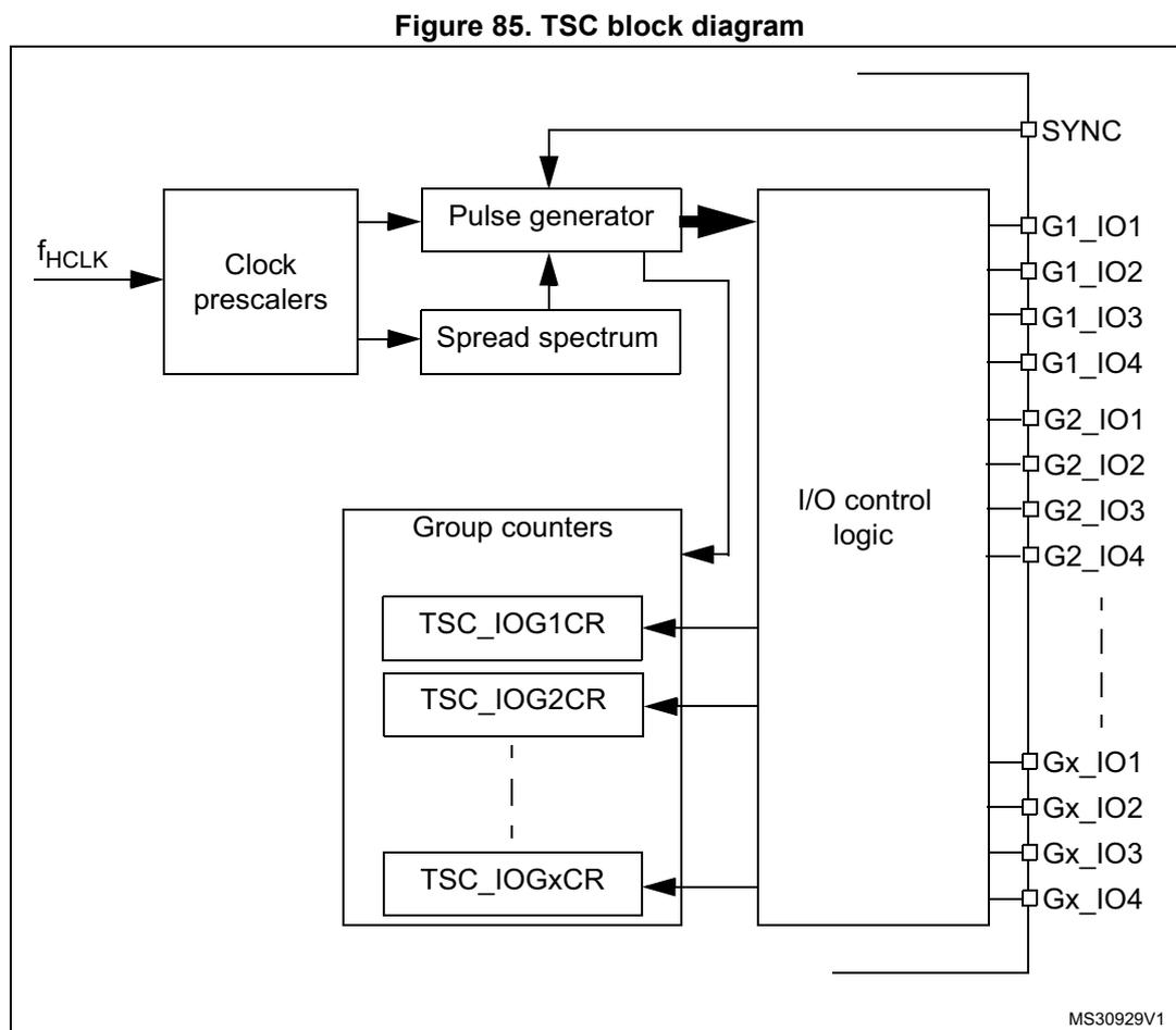
Figure 85. TSC block diagram
20.4.2 Surface charge transfer acquisition overview
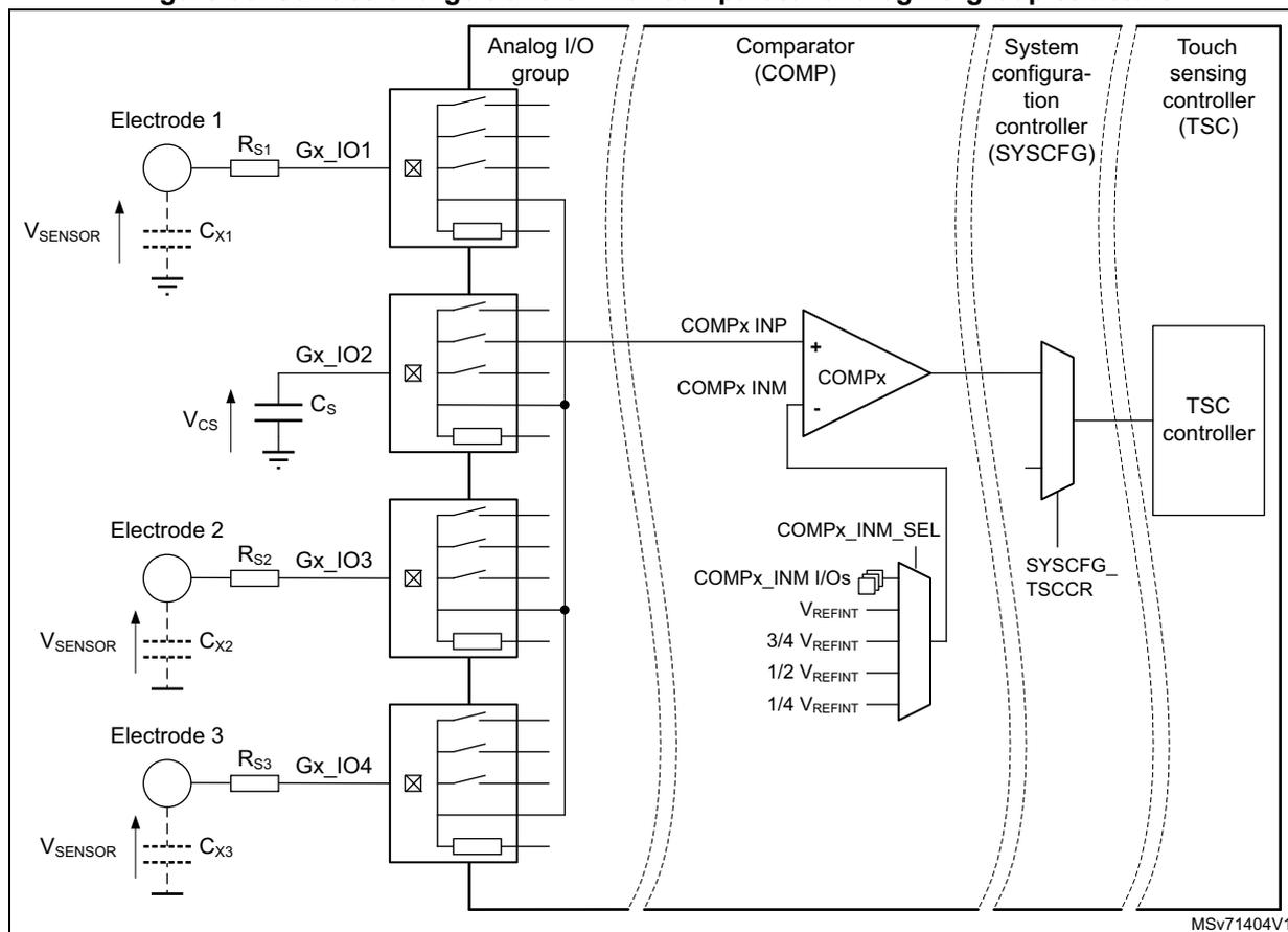
The surface charge transfer acquisition is a proven, robust and efficient way to measure a capacitance. It uses a minimum number of external components to operate with a single ended electrode type. This acquisition is designed around an analog I/O group composed of up to four GPIOs (see Figure 86 ). Several analog I/O groups are available to allow the acquisition of several capacitive sensing channels simultaneously and to support a larger number of capacitive sensing channels. Within a same analog I/O group, the acquisition of the capacitive sensing channels is sequential.
One of the GPIOs is dedicated to the sampling capacitor \( C_S \) . Only one sampling capacitor I/O per analog I/O group must be enabled at a time.
The remaining GPIOs are dedicated to the electrodes and are commonly called channels. For some specific needs (such as proximity detection), it is possible to simultaneously enable more than one channel per analog I/O group.
Figure 86. Surface charge transfer analog I/O group structure
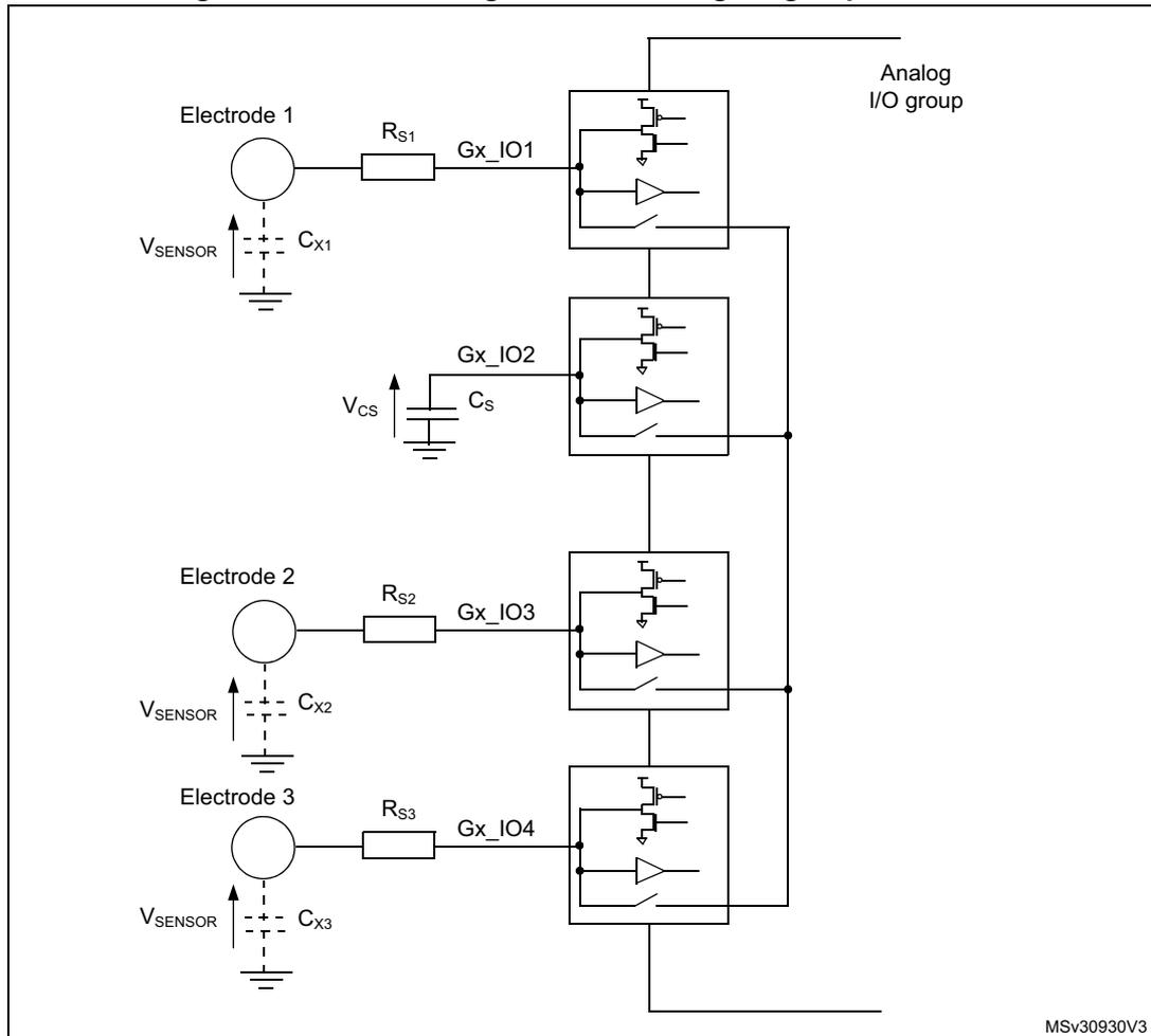
Note: Gx_IOy where x is the analog I/O group number and y the GPIO number within the selected group.
The surface charge transfer acquisition principle consists of charging an electrode capacitance (C X ) and transferring a part of the accumulated charge into a sampling capacitor (C S ). This sequence is repeated until the voltage across C S reaches a given threshold (V IH in our case). The number of charge transfers required to reach the threshold is a direct representation of the size of the electrode capacitance.
Table 106 details the charge transfer acquisition sequence of the capacitive sensing channel 1. States 3 to 7 are repeated until the voltage across C S reaches the given threshold. The same sequence applies to the acquisition of the other channels. The electrode serial resistor R S improves the ESD immunity of the solution.
Table 106. Acquisition sequence summary
| State | Gx_IO1 (channel) | Gx_IO2 (sampling) | Gx_IO3 (channel) | Gx_IO4 (channel) | State description |
|---|---|---|---|---|---|
| #1 | Input floating with analog switch closed | Output open-drain low with analog switch closed | Input floating with analog switch closed | Discharge all \( C_X \) and \( C_S \) | |
| #2 | Input floating | Dead time | |||
| #3 | Output push-pull high | Input floating | Charge \( C_{X1} \) | ||
| #4 | Input floating | Dead time | |||
| #5 | Input floating with analog switch closed | Input floating | Charge transfer from \( C_{X1} \) to \( C_S \) | ||
| #6 | Input floating | Dead time | |||
| #7 | Input floating | Measure \( C_S \) voltage | |||
Note: Gx_IOy where x is the analog I/O group number and y the GPIO number within the selected group.
The voltage variation over the time on the sampling capacitor \( C_S \) is detailed below (refer to Figure 86 for \( V_{SENSOR} \) and \( V_{CS} \) definition):
Figure 87. Sampling capacitor voltage variation
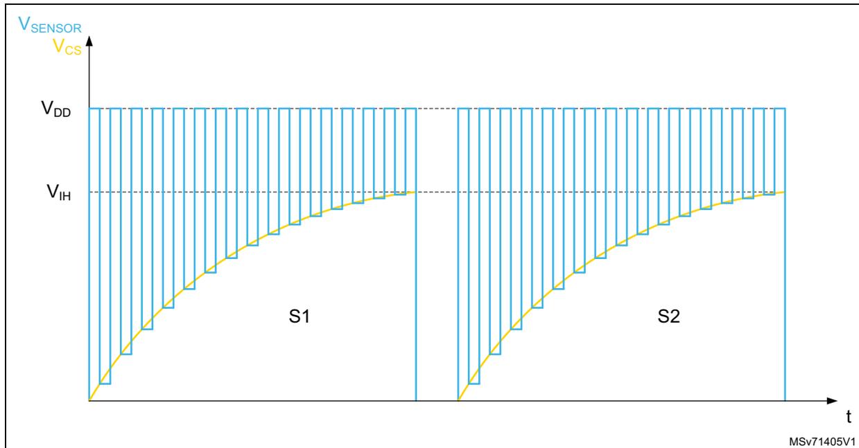
The graph illustrates the voltage variation of the sampling capacitor \( V_{CS} \) over time \( t \) . The y-axis is labeled with \( V_{SENSOR} \) and \( V_{CS} \) at the top, \( V_{DD} \) and \( V_{IH} \) as reference levels. The x-axis is labeled \( t \) . The graph shows two acquisition sequences, S1 and S2. In each sequence, a series of blue vertical lines represent the sampling pulses. The yellow curve represents the voltage \( V_{CS} \) , which starts at a low voltage and gradually increases towards \( V_{IH} \) during the sequence. The voltage drops to a low level between the two sequences. The text 'MSV71405V1' is visible in the bottom right corner of the graph area.
20.4.3 Reset and clocks
The TSC clock source is the AHB clock (HCLK). Two programmable prescalers are used to generate the pulse generator and the spread spectrum internal clocks:
- • The pulse generator clock (PGCLK) is defined using the PGPSC[2:0] bits of the TSC_CR register
- • The spread spectrum clock (SSCLK) is defined using the SSPSC bit of the TSC_CR register
The reset and clock controller (RCC) provides dedicated bits to enable the touch sensing controller clock and to reset this peripheral. For more information, refer to Section 5: Reset and clock control (RCC) .
20.4.4 Charge transfer acquisition sequence
An example of a charge transfer acquisition sequence is detailed in Figure 88 .
Figure 88. Charge transfer acquisition sequence
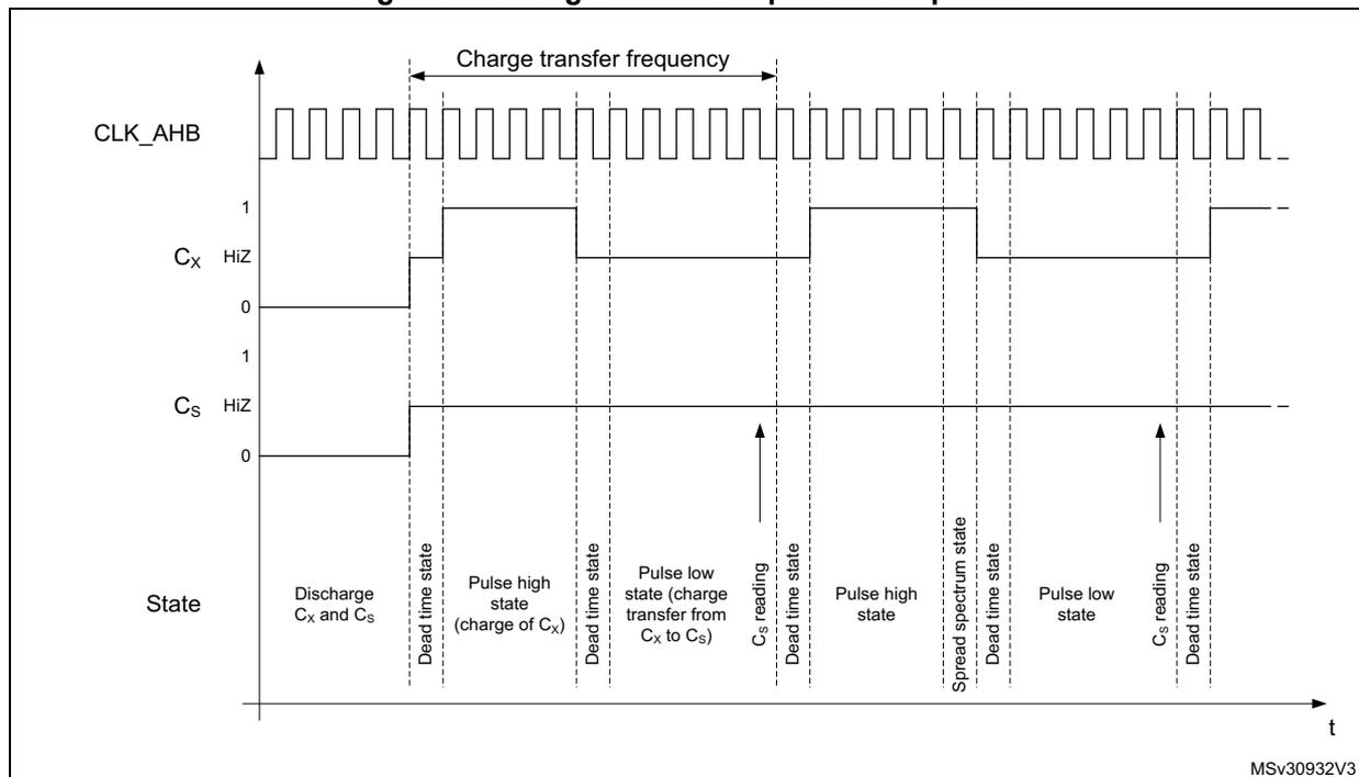
For higher flexibility, the charge transfer frequency is fully configurable. Both the pulse high state (charge of \( C_X \) ) and the pulse low state (transfer of charge from \( C_X \) to \( C_S \) ) duration can be defined using the CTPH[3:0] and CTPL[3:0] bits in the TSC_CR register. The standard range for the pulse high and low states duration is 500 ns to 2 µs. To ensure a correct measurement of the electrode capacitance, the pulse high state duration must be set to ensure that \( C_X \) is always fully charged.
A dead time where both the sampling capacitor I/O and the channel I/O are in input floating state is inserted between the pulse high and low states to ensure an optimum charge transfer acquisition sequence. This state duration is 1 period of HCLK.
At the end of the pulse high state and if the spread spectrum feature is enabled, a variable number of periods of the SSCLK clock are added.
The reading of the sampling capacitor I/O, to determine if the voltage across \( C_S \) has reached the given threshold, is performed at the end of the pulse low state.
Note: The following TSC control register configurations are forbidden:
- • bits PGPSC are set to 000 and bits CTPL are set to 0001
- • bits PGPSC are set to 001 and bits CTPL are set to 0000
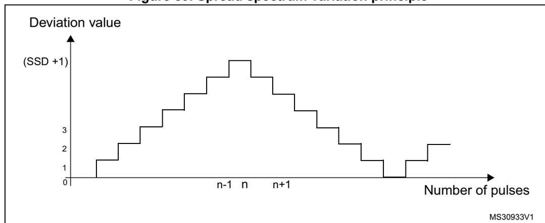
20.4.5 Spread spectrum feature
The spread spectrum feature generates a variation of the charge transfer frequency. This is done to improve the robustness of the charge transfer acquisition in noisy environments and also to reduce the induced emission. The maximum frequency variation is in the range of 10% to 50% of the nominal charge transfer period. For instance, for a nominal charge transfer frequency of 250 kHz (4 \( \mu\text{s} \) ), the typical spread spectrum deviation is 10% (400 ns) which leads to a minimum charge transfer frequency of ~227 kHz.
In practice, the spread spectrum consists of adding a variable number of SSCLK periods to the pulse high state using the principle shown below:
Figure 89. Spread spectrum variation principle
The table below details the maximum frequency deviation with different HCLK settings:
Table 107. Spread spectrum deviation versus AHB clock frequency
| \( f_{\text{HCLK}} \) | Spread spectrum step | Maximum spread spectrum deviation |
|---|---|---|
| 48 MHz | 20.8 ns | 5333.3 ns |
The spread spectrum feature can be disabled/enabled using the SSE bit in the TSC_CR register. The frequency deviation is also configurable to accommodate the device HCLK clock frequency and the selected charge transfer frequency through the SSPSC and SSD[6:0] bits in the TSC_CR register.
20.4.6 Max count error
The max count error prevents long acquisition times resulting from a faulty capacitive sensing channel. It consists of specifying a maximum count value for the analog I/O group counters. This maximum count value is specified using the MCV[2:0] bits in the TSC_CR register. As soon as an acquisition group counter reaches this maximum value, the ongoing acquisition is stopped and the end of acquisition (EOAF bit) and max count error (MCEF bit) flags are both set. An interrupt can also be generated if the corresponding end of acquisition (EOAIE bit) or/and max count error (MCEIE bit) interrupt enable bits are set.
20.4.7 Sampling capacitor I/O and channel I/O mode selection
To allow the GPIOs to be controlled by the touch sensing controller, the corresponding alternate function must be enabled through the standard GPIO registers and the GPIOxAFR registers.
The GPIOs modes controlled by the TSC are defined using the TSC_IOSCR and TSC_IOCCR register.
When there is no ongoing acquisition, all the I/Os controlled by the touch sensing controller are in default state. While an acquisition is ongoing, only unused I/Os (neither defined as sampling capacitor I/O nor as channel I/O) are in default state. The IODEF bit in the TSC_CR register defines the configuration of the I/Os which are in default state. The table below summarizes the configuration of the I/O depending on its mode.
Table 108. I/O state depending on its mode and IODEF bit value
| IODEF bit | Acquisition status | Unused I/O mode | Channel I/O mode | Sampling capacitor I/O mode |
|---|---|---|---|---|
| 0 (output push-pull low) | No | Output push-pull low | Output push-pull low | Output push-pull low |
| 0 (output push-pull low) | Ongoing | Output push-pull low | - | - |
| 1 (input floating) | No | Input floating | Input floating | Input floating |
| 1 (input floating) | Ongoing | Input floating | - | - |
Unused I/O mode
An unused I/O corresponds to a GPIO controlled by the TSC peripheral but not defined as an electrode I/O nor as a sampling capacitor I/O.
Sampling capacitor I/O mode
To allow the control of the sampling capacitor I/O by the TSC peripheral, the corresponding GPIO must be first set to alternate output open drain mode and then the corresponding Gx_IOy bit in the TSC_IOSCR register must be set.
Only one sampling capacitor per analog I/O group must be enabled at a time.
Channel I/O mode
To allow the control of the channel I/O by the TSC peripheral, the corresponding GPIO must be first set to alternate output push-pull mode and the corresponding Gx_IOy bit in the TSC_IOCCR register must be set.
For proximity detection where a higher equivalent electrode surface is required or to speed-up the acquisition process, it is possible to enable and simultaneously acquire several channels belonging to the same analog I/O group.
Note: During the acquisition phase and even if the TSC peripheral alternate function is not enabled, as soon as the TSC_IOSCR or TSC_IOCCR bit is set, the corresponding GPIO analog switch is automatically controlled by the touch sensing controller.
20.4.8 Acquisition mode
The touch sensing controller offers two acquisition modes:
- • Normal acquisition mode: the acquisition starts as soon as the START bit in the TSC_CR register is set.
- • Synchronized acquisition mode: the acquisition is enabled by setting the START bit in the TSC_CR register but only starts upon the detection of a falling edge or a rising edge and high level on the SYNC input pin. This mode is useful for synchronizing the capacitive sensing channels acquisition with an external signal without additional CPU load.
The GxE bits in the TSC_IOGCSR registers specify which analog I/O groups are enabled (corresponding counter is counting). The C S voltage of a disabled analog I/O group is not monitored and this group does not participate in the triggering of the end of acquisition flag. However, if the disabled analog I/O group contains some channels, they are pulsed.
When the C S voltage of an enabled analog I/O group reaches the given threshold, the corresponding GxS bit of the TSC_IOGCSR register is set. When the acquisition of all enabled analog I/O groups is complete (all GxS bits of all enabled analog I/O groups are set), the EOAF flag in the TSC_ISR register is set. An interrupt request is generated if the EOAIIE bit in the TSC_IER register is set.
In the case that a max count error is detected, the ongoing acquisition is stopped and both the EOAF and MCEF flags in the TSC_ISR register are set. Interrupt requests can be generated for both events if the corresponding bits (EOAIIE and MCEIIE bits of the TSCIER register) are set. Note that when the max count error is detected the remaining GxS bits in the enabled analog I/O groups are not set.
To clear the interrupt flags, the corresponding EOAIIC and MCEIIC bits in the TSC_ICR register must be set.
The analog I/O group counters are cleared when a new acquisition is started. They are updated with the number of charge transfer cycles generated on the corresponding channel(s) upon the completion of the acquisition.
20.4.9 I/O hysteresis and analog switch control
In order to offer a higher flexibility, the touch sensing controller is able to take the control of the Schmitt trigger hysteresis and analog switch of each Gx_IOy. This control is available whatever the I/O control mode is (controlled by standard GPIO registers or other peripherals) assuming that the touch sensing controller is enabled. This may be useful to perform a different acquisition sequence or for other purposes.
In order to improve the system immunity, the Schmitt trigger hysteresis of the GPIOs controlled by the TSC must be disabled by resetting the corresponding Gx_IOy bit in the TSC_IOHCR register.
20.5 TSC low-power modes
Table 109. Effect of low-power modes on TSC
| Mode | Description |
|---|---|
| Sleep | No effect. Peripheral interrupts cause the device to exit Sleep mode. |
| Low power run | No effect. |
| Low power sleep | No effect. Peripheral interrupts cause the device to exit Low-power sleep mode. |
| Stop 0 / Stop 1 | Peripheral registers content is kept. |
| Stop 2 | |
| Standby | Powered-down. The peripheral must be reinitialized after exiting Standby or Shutdown mode. |
| Shutdown |
20.5.1 Comparator usage overview
This low-power mode requires that the GPIO dedicated to the sampling capacitor \( C_S \) has both the TSC alternate function (TSC_Gx_IOy) and the COMP alternate function (COMPx_INP) available, see product datasheet.
In this case, the TSC peripheral has the possibility to use the microcontroller internal comparator to achieve lower power consumption.
The method uses the same principle as the surface charge transfer acquisition that is the acquisition of the different sensors is automatically stopped when the voltage on the sampling capacitor reaches a certain threshold.
Figure 90. Surface charge transfer with comparator analog I/O group structure
Unlike charge transfer acquisition (where the threshold is fixed \( = V_{IH} \) ), here the threshold is programmable. The sampling capacitor is internally redirected to the comparator input in order to offer a programmable voltage threshold value \( V_{COMP} \) based on \( V_{REFINT} \) . The possible configurations are about 0.3, 0.6, 0.9 or 1.2 V (corresponding to \( 1/4 V_{REFINT} \) , \( 1/2 V_{REFINT} \) , \( 3/4 V_{REFINT} \) or \( V_{REFINT} \) ).
\( V_{REFINT} \) is the bandgap voltage ( \( \sim 1.2 \) V).
By reducing the voltage threshold, the acquisition time is shortened which in turn reduces the power consumption.
The selection of the threshold value is a compromise between sensor acquisition time (the lowest the threshold the best) and sensor sensitivity (the highest the threshold the best).
Figure 91 below compares the normal mode and the comparator mode (see Figure 90 for \( V_{SENSOR} \) and \( V_{CS} \) definition).
The SYSCFG_TSCCR register should be set appropriately in order to configure the MUX allowing the use of the comparator mode instead of the usual TSC mode (see device reference manual).
Figure 91. Sensor voltage variation for both normal and comparator mode
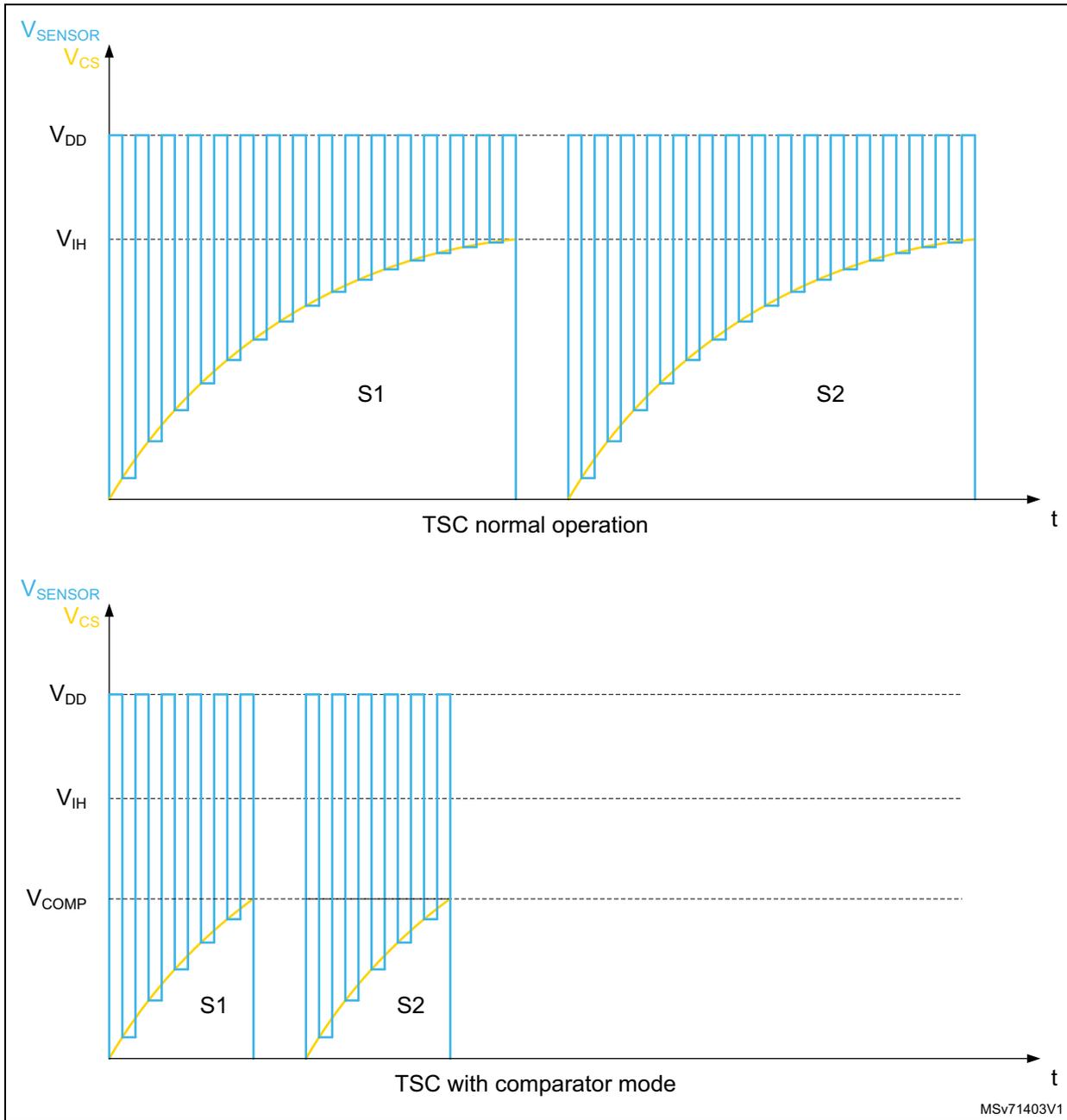
The figure consists of two vertically stacked plots. The top plot, labeled 'TSC normal operation', shows the sensor voltage (V_SENSOR) on the y-axis against time (t) on the x-axis. The y-axis has markers for V_CS, V_DD, and V_IH. The voltage starts at a low level and rises in a series of steps, following a smooth curve towards V_IH. The rising phase is labeled 'S1'. After a gap, the voltage starts rising again towards V_IH, labeled 'S2'. Vertical blue lines represent periodic charging pulses. The bottom plot, labeled 'TSC with comparator mode', shows the same sensor voltage over time. The y-axis has markers for V_CS, V_DD, V_IH, and V_COMP. The voltage rises in steps towards V_COMP. The rising phases are labeled 'S1' and 'S2'. Vertical blue lines represent periodic charging pulses. The text 'MSV71403V1' is in the bottom right corner.
Using the internal comparator, the acquisition time is consequently reduced. This implies that the number of counts needed to reach the threshold is also reduced, thus, the TSC peripheral achieves lower power consumption.
The COMPx_INM_SEL and COMPx_INP_SEL bitfields used to configure the comparator are available in Section 17.6.1: Comparator 1 control and status register (COMP1_CSR) and Section 17.6.2: Comparator 2 control and status register (COMP2_CSR) .
20.6 TSC interrupts
Table 110. Interrupt control bits
| Interrupt event | Enable control bit | Event flag | Clear flag bit | Exit the Sleep mode | Exit the Stop mode | Exit the Standby mode |
|---|---|---|---|---|---|---|
| End of acquisition | EOAIE | EOAIF | EOAIC | Yes | No | No |
| Max count error | MCEIE | MCEIF | MCEIC | Yes | No | No |
20.7 TSC registers
Refer to Section 1.2 of the reference manual for a list of abbreviations used in register descriptions.
The peripheral registers can be accessed by words (32-bit).
20.7.1 TSC control register (TSC_CR)
Address offset: 0x00
Reset value: 0x0000 0000
| 31 | 30 | 29 | 28 | 27 | 26 | 25 | 24 | 23 | 22 | 21 | 20 | 19 | 18 | 17 | 16 |
|---|---|---|---|---|---|---|---|---|---|---|---|---|---|---|---|
| CTPH[3:0] | CTPL[3:0] | SSD[6:0] | SSE | ||||||||||||
| rw | rw | rw | rw | rw | rw | rw | rw | rw | rw | rw | rw | rw | rw | rw | rw |
| 15 | 14 | 13 | 12 | 11 | 10 | 9 | 8 | 7 | 6 | 5 | 4 | 3 | 2 | 1 | 0 |
| SSPSC | PGPSC[2:0] | Res. | Res. | Res. | Res. | MCV[2:0] | IODEF | SYNC POL | AM | START | TSCE | ||||
| rw | rw | rw | rw | rw | rw | rw | rw | rw | rw | rw | rw | ||||
These bits are set and cleared by software. They define the duration of the high state of the charge transfer pulse (charge of \( C_X \) ).
0000: \( 1 \times t_{PGCLK} \)
0001: \( 2 \times t_{PGCLK} \)
...
1111: \( 16 \times t_{PGCLK} \)
Note: These bits must not be modified when an acquisition is ongoing.
Bits 27:24 CTPL[3:0] : Charge transfer pulse lowThese bits are set and cleared by software. They define the duration of the low state of the charge transfer pulse (transfer of charge from \( C_X \) to \( C_S \) ).
0000: \( 1 \times t_{PGCLK} \)
0001: \( 2 \times t_{PGCLK} \)
...
1111: \( 16 \times t_{PGCLK} \)
Note: These bits must not be modified when an acquisition is ongoing.
Note: Some configurations are forbidden. Refer to the Section 20.4.4: Charge transfer acquisition sequence for details.
Bits 23:17 SSD[6:0] : Spread spectrum deviationThese bits are set and cleared by software. They define the spread spectrum deviation which consists in adding a variable number of periods of the SSCLK clock to the charge transfer pulse high state.
0000000: \( 1 \times t_{SSCLK} \)
0000001: \( 2 \times t_{SSCLK} \)
...
1111111: \( 128 \times t_{SSCLK} \)
Note: These bits must not be modified when an acquisition is ongoing.
Bit 16 SSE : Spread spectrum enableThis bit is set and cleared by software to enable/disable the spread spectrum feature.
0: Spread spectrum disabled
1: Spread spectrum enabled
Note: This bit must not be modified when an acquisition is ongoing.
Bit 15 SSPSC : Spread spectrum prescalerThis bit is set and cleared by software. It selects the AHB clock divider used to generate the spread spectrum clock (SSCLK).
0: \( f_{HCLK} \)
1: \( f_{HCLK} / 2 \)
Note: This bit must not be modified when an acquisition is ongoing.
Bits 14:12 PGPSC[2:0] : Pulse generator prescalerThese bits are set and cleared by software. They select the AHB clock divider used to generate the pulse generator clock (PGCLK).
000:
\(
f_{HCLK}
\)
001:
\(
f_{HCLK} / 2
\)
010:
\(
f_{HCLK} / 4
\)
011:
\(
f_{HCLK} / 8
\)
100:
\(
f_{HCLK} / 16
\)
101:
\(
f_{HCLK} / 32
\)
110:
\(
f_{HCLK} / 64
\)
111:
\(
f_{HCLK} / 128
\)
Note: These bits must not be modified when an acquisition is ongoing.
Note: Some configurations are forbidden. Refer to the Section 20.4.4: Charge transfer acquisition sequence for details.
Bits 11:8 Reserved, must be kept at reset value.
Bits 7:5 MCV[2:0] : Max count valueThese bits are set and cleared by software. They define the maximum number of charge transfer pulses that can be generated before a max count error is generated.
000: 255
001: 511
010: 1023
011: 2047
100: 4095
101: 8191
110: 16383
111: reserved
Note: These bits must not be modified when an acquisition is ongoing.
Bit 4 IODEF : I/O Default modeThis bit is set and cleared by software. It defines the configuration of all the TSC I/Os when there is no ongoing acquisition. When there is an ongoing acquisition, it defines the configuration of all unused I/Os (not defined as sampling capacitor I/O or as channel I/O).
0: I/Os are forced to output push-pull low
1: I/Os are in input floating
Note: This bit must not be modified when an acquisition is ongoing.
Bit 3 SYNCPOL : Synchronization pin polarityThis bit is set and cleared by software to select the polarity of the synchronization input pin.
0: Falling edge only
1: Rising edge and high level
Bit 2 AM : Acquisition mode
This bit is set and cleared by software to select the acquisition mode.
0: Normal acquisition mode (acquisition starts as soon as START bit is set)
1: Synchronized acquisition mode (acquisition starts if START bit is set and when the selected signal is detected on the SYNC input pin)
Note: This bit must not be modified when an acquisition is ongoing.
Bit 1 START : Start a new acquisition
This bit is set by software to start a new acquisition. It is cleared by hardware as soon as the acquisition is complete or by software to cancel the ongoing acquisition.
0: Acquisition not started
1: Start a new acquisition
Bit 0 TSCE : Touch sensing controller enable
This bit is set and cleared by software to enable/disable the touch sensing controller.
0: Touch sensing controller disabled
1: Touch sensing controller enabled
Note: When the touch sensing controller is disabled, TSC registers settings have no effect.
20.7.2 TSC interrupt enable register (TSC_IER)
Address offset: 0x04
Reset value: 0x0000 0000
| 31 | 30 | 29 | 28 | 27 | 26 | 25 | 24 | 23 | 22 | 21 | 20 | 19 | 18 | 17 | 16 |
|---|---|---|---|---|---|---|---|---|---|---|---|---|---|---|---|
| Res. | Res. | Res. | Res. | Res. | Res. | Res. | Res. | Res. | Res. | Res. | Res. | Res. | Res. | Res. | Res. |
| 15 | 14 | 13 | 12 | 11 | 10 | 9 | 8 | 7 | 6 | 5 | 4 | 3 | 2 | 1 | 0 |
| Res. | Res. | Res. | Res. | Res. | Res. | Res. | Res. | Res. | Res. | Res. | Res. | Res. | Res. | MCEIE | EOAIE |
| rw | rw |
Bits 31:2 Reserved, must be kept at reset value.
Bit 1 MCEIE : Max count error interrupt enable
This bit is set and cleared by software to enable/disable the max count error interrupt.
0: Max count error interrupt disabled
1: Max count error interrupt enabled
Bit 0 EOAIE : End of acquisition interrupt enable
This bit is set and cleared by software to enable/disable the end of acquisition interrupt.
0: End of acquisition interrupt disabled
1: End of acquisition interrupt enabled
20.7.3 TSC interrupt clear register (TSC_ICR)
Address offset: 0x08
Reset value: 0x0000 0000
| 31 | 30 | 29 | 28 | 27 | 26 | 25 | 24 | 23 | 22 | 21 | 20 | 19 | 18 | 17 | 16 |
|---|---|---|---|---|---|---|---|---|---|---|---|---|---|---|---|
| Res. | Res. | Res. | Res. | Res. | Res. | Res. | Res. | Res. | Res. | Res. | Res. | Res. | Res. | Res. | Res. |
| 15 | 14 | 13 | 12 | 11 | 10 | 9 | 8 | 7 | 6 | 5 | 4 | 3 | 2 | 1 | 0 |
| Res. | Res. | Res. | Res. | Res. | Res. | Res. | Res. | Res. | Res. | Res. | Res. | Res. | Res. | MCEIC | EOAIC |
| nw | nw |
Bits 31:2 Reserved, must be kept at reset value.
Bit 1 MCEIC : Max count error interrupt clear
This bit is set by software to clear the max count error flag and it is cleared by hardware when the flag is reset. Writing a 0 has no effect.
0: No effect
1: Clears the corresponding MCEF of the TSC_ISR register
Bit 0 EOAIC : End of acquisition interrupt clear
This bit is set by software to clear the end of acquisition flag and it is cleared by hardware when the flag is reset. Writing a 0 has no effect.
0: No effect
1: Clears the corresponding EOAF of the TSC_ISR register
20.7.4 TSC interrupt status register (TSC_ISR)
Address offset: 0x0C
Reset value: 0x0000 0000
| 31 | 30 | 29 | 28 | 27 | 26 | 25 | 24 | 23 | 22 | 21 | 20 | 19 | 18 | 17 | 16 |
|---|---|---|---|---|---|---|---|---|---|---|---|---|---|---|---|
| Res. | Res. | Res. | Res. | Res. | Res. | Res. | Res. | Res. | Res. | Res. | Res. | Res. | Res. | Res. | Res. |
| 15 | 14 | 13 | 12 | 11 | 10 | 9 | 8 | 7 | 6 | 5 | 4 | 3 | 2 | 1 | 0 |
| Res. | Res. | Res. | Res. | Res. | Res. | Res. | Res. | Res. | Res. | Res. | Res. | Res. | Res. | MCEF | EOAF |
| r | r |
Bits 31:2 Reserved, must be kept at reset value.
Bit 1 MCEF : Max count error flag
This bit is set by hardware as soon as an analog I/O group counter reaches the max count value specified. It is cleared by software writing 1 to the bit MCEIC of the TSC_ICR register.
0: No max count error (MCE) detected
1: Max count error (MCE) detected
Bit 0 EOAF : End of acquisition flag
This bit is set by hardware when the acquisition of all enabled group is complete (all GxS bits of all enabled analog I/O groups are set or when a max count error is detected). It is cleared by software writing 1 to the bit EOAIC of the TSC_ICR register.
0: Acquisition is ongoing or not started
1: Acquisition is complete
20.7.5 TSC I/O hysteresis control register (TSC_IOHCR)
Address offset: 0x10
Reset value: 0xFFFF FFFF
| 31 | 30 | 29 | 28 | 27 | 26 | 25 | 24 | 23 | 22 | 21 | 20 | 19 | 18 | 17 | 16 |
|---|---|---|---|---|---|---|---|---|---|---|---|---|---|---|---|
| Res. | Res. | Res. | Res. | G7_IO4 | G7_IO3 | G7_IO2 | G7_IO1 | G6_IO4 | G6_IO3 | G6_IO2 | G6_IO1 | G5_IO4 | G5_IO3 | G5_IO2 | G5_IO1 |
| rw | rw | rw | rw | rw | rw | rw | rw | rw | rw | rw | rw | ||||
| 15 | 14 | 13 | 12 | 11 | 10 | 9 | 8 | 7 | 6 | 5 | 4 | 3 | 2 | 1 | 0 |
| G4_IO4 | G4_IO3 | G4_IO2 | G4_IO1 | G3_IO4 | G3_IO3 | G3_IO2 | G3_IO1 | G2_IO4 | G2_IO3 | G2_IO2 | G2_IO1 | G1_IO4 | G1_IO3 | G1_IO2 | G1_IO1 |
| rw | rw | rw | rw | rw | rw | rw | rw | rw | rw | rw | rw | rw | rw | rw | rw |
Bits 31:28 Reserved, must be kept at reset value.
Bits 27:0 Gx_IOy : Gx_IOy Schmitt trigger hysteresis mode
These bits are set and cleared by software to enable/disable the Gx_IOy Schmitt trigger hysteresis.
0: Gx_IOy Schmitt trigger hysteresis disabled
1: Gx_IOy Schmitt trigger hysteresis enabled
Note: These bits control the I/O Schmitt trigger hysteresis whatever the I/O control mode is (even if controlled by standard GPIO registers).
20.7.6 TSC I/O analog switch control register (TSC_IOASCR)
Address offset: 0x18
Reset value: 0x0000 0000
| 31 | 30 | 29 | 28 | 27 | 26 | 25 | 24 | 23 | 22 | 21 | 20 | 19 | 18 | 17 | 16 |
|---|---|---|---|---|---|---|---|---|---|---|---|---|---|---|---|
| Res. | Res. | Res. | Res. | G7_IO4 | G7_IO3 | G7_IO2 | G7_IO1 | G6_IO4 | G6_IO3 | G6_IO2 | G6_IO1 | G5_IO4 | G5_IO3 | G5_IO2 | G5_IO1 |
| rw | rw | rw | rw | rw | rw | rw | rw | rw | rw | rw | rw | ||||
| 15 | 14 | 13 | 12 | 11 | 10 | 9 | 8 | 7 | 6 | 5 | 4 | 3 | 2 | 1 | 0 |
| G4_IO4 | G4_IO3 | G4_IO2 | G4_IO1 | G3_IO4 | G3_IO3 | G3_IO2 | G3_IO1 | G2_IO4 | G2_IO3 | G2_IO2 | G2_IO1 | G1_IO4 | G1_IO3 | G1_IO2 | G1_IO1 |
| rw | rw | rw | rw | rw | rw | rw | rw | rw | rw | rw | rw | rw | rw | rw | rw |
Bits 31:28 Reserved, must be kept at reset value.
Bits 27:0 Gx_IOy : Gx_IOy analog switch enable
These bits are set and cleared by software to enable/disable the Gx_IOy analog switch.
0: Gx_IOy analog switch disabled (opened)
1: Gx_IOy analog switch enabled (closed)
Note: These bits control the I/O analog switch whatever the I/O control mode is (even if controlled by standard GPIO registers).
20.7.7 TSC I/O sampling control register (TSC_IOSCR)
Address offset: 0x20
Reset value: 0x0000 0000
| 31 | 30 | 29 | 28 | 27 | 26 | 25 | 24 | 23 | 22 | 21 | 20 | 19 | 18 | 17 | 16 |
|---|---|---|---|---|---|---|---|---|---|---|---|---|---|---|---|
| Res. | Res. | Res. | Res. | G7_IO4 | G7_IO3 | G7_IO2 | G7_IO1 | G6_IO4 | G6_IO3 | G6_IO2 | G6_IO1 | G5_IO4 | G5_IO3 | G5_IO2 | G5_IO1 |
| rw | rw | rw | rw | rw | rw | rw | rw | rw | rw | rw | rw | ||||
| 15 | 14 | 13 | 12 | 11 | 10 | 9 | 8 | 7 | 6 | 5 | 4 | 3 | 2 | 1 | 0 |
| G4_IO4 | G4_IO3 | G4_IO2 | G4_IO1 | G3_IO4 | G3_IO3 | G3_IO2 | G3_IO1 | G2_IO4 | G2_IO3 | G2_IO2 | G2_IO1 | G1_IO4 | G1_IO3 | G1_IO2 | G1_IO1 |
| rw | rw | rw | rw | rw | rw | rw | rw | rw | rw | rw | rw | rw | rw | rw | rw |
Bits 31:28 Reserved, must be kept at reset value.
Bits 27:0 Gx_IOy : Gx_IOy sampling mode
These bits are set and cleared by software to configure the Gx_IOy as a sampling capacitor I/O. Only one I/O per analog I/O group must be defined as sampling capacitor.
0: Gx_IOy unused
1: Gx_IOy used as sampling capacitor
Note: These bits must not be modified when an acquisition is ongoing.
During the acquisition phase and even if the TSC peripheral alternate function is not enabled, as soon as the TSC_IOSCR bit is set, the corresponding GPIO analog switch is automatically controlled by the touch sensing controller.
20.7.8 TSC I/O channel control register (TSC_IOCCR)
Address offset: 0x28
Reset value: 0x0000 0000
| 31 | 30 | 29 | 28 | 27 | 26 | 25 | 24 | 23 | 22 | 21 | 20 | 19 | 18 | 17 | 16 |
|---|---|---|---|---|---|---|---|---|---|---|---|---|---|---|---|
| Res. | Res. | Res. | Res. | G7_IO4 | G7_IO3 | G7_IO2 | G7_IO1 | G6_IO4 | G6_IO3 | G6_IO2 | G6_IO1 | G5_IO4 | G5_IO3 | G5_IO2 | G5_IO1 |
| rw | rw | rw | rw | rw | rw | rw | rw | rw | rw | rw | rw | ||||
| 15 | 14 | 13 | 12 | 11 | 10 | 9 | 8 | 7 | 6 | 5 | 4 | 3 | 2 | 1 | 0 |
| G4_IO4 | G4_IO3 | G4_IO2 | G4_IO1 | G3_IO4 | G3_IO3 | G3_IO2 | G3_IO1 | G2_IO4 | G2_IO3 | G2_IO2 | G2_IO1 | G1_IO4 | G1_IO3 | G1_IO2 | G1_IO1 |
| rw | rw | rw | rw | rw | rw | rw | rw | rw | rw | rw | rw | rw | rw | rw | rw |
Bits 31:28 Reserved, must be kept at reset value.
Bits 27:0 Gx_IOy : Gx_IOy channel mode
These bits are set and cleared by software to configure the Gx_IOy as a channel I/O.
0: Gx_IOy unused
1: Gx_IOy used as channel
Note: These bits must not be modified when an acquisition is ongoing.
During the acquisition phase and even if the TSC peripheral alternate function is not enabled, as soon as the TSC_IOCCR bit is set, the corresponding GPIO analog switch is automatically controlled by the touch sensing controller.
20.7.9 TSC I/O group control status register (TSC_IOGCSR)
Address offset: 0x30
Reset value: 0x0000 0000
| 31 | 30 | 29 | 28 | 27 | 26 | 25 | 24 | 23 | 22 | 21 | 20 | 19 | 18 | 17 | 16 |
|---|---|---|---|---|---|---|---|---|---|---|---|---|---|---|---|
| Res. | Res. | Res. | Res. | Res. | Res. | Res. | Res. | Res. | G7S | G6S | G5S | G4S | G3S | G2S | G1S |
| r | r | r | r | r | r | r | |||||||||
| 15 | 14 | 13 | 12 | 11 | 10 | 9 | 8 | 7 | 6 | 5 | 4 | 3 | 2 | 1 | 0 |
| Res. | Res. | Res. | Res. | Res. | Res. | Res. | Res. | Res. | G7E | G6E | G5E | G4E | G3E | G2E | G1E |
| rw | rw | rw | rw | rw | rw | rw |
Bits 31:23 Reserved, must be kept at reset value.
Bits 22:16 GxS : Analog I/O group x status
These bits are set by hardware when the acquisition on the corresponding enabled analog I/O group x is complete. They are cleared by hardware when a new acquisition is started.
0: Acquisition on analog I/O group x is ongoing or not started
1: Acquisition on analog I/O group x is complete
Note: When a max count error is detected the remaining GxS bits of the enabled analog I/O groups are not set.
Bits 15:7 Reserved, must be kept at reset value.
Bits 6:0 GxE : Analog I/O group x enable
These bits are set and cleared by software to enable/disable the acquisition (counter is counting) on the corresponding analog I/O group x.
0: Acquisition on analog I/O group x disabled
1: Acquisition on analog I/O group x enabled
20.7.10 TSC I/O group x counter register (TSC_IOGxCR)
x represents the analog I/O group number.
Address offset: 0x30 + 0x04 * x, (x = 1 to 7)
Reset value: 0x0000 0000
| 31 | 30 | 29 | 28 | 27 | 26 | 25 | 24 | 23 | 22 | 21 | 20 | 19 | 18 | 17 | 16 |
|---|---|---|---|---|---|---|---|---|---|---|---|---|---|---|---|
| Res. | Res. | Res. | Res. | Res. | Res. | Res. | Res. | Res. | Res. | Res. | Res. | Res. | Res. | Res. | Res. |
| 15 | 14 | 13 | 12 | 11 | 10 | 9 | 8 | 7 | 6 | 5 | 4 | 3 | 2 | 1 | 0 |
| Res. | Res. | CNT[13:0] | |||||||||||||
| r | r | r | r | r | r | r | r | r | r | r | r | r | r | ||
Bits 31:14 Reserved, must be kept at reset value.
Bits 13:0 CNT[13:0] : Counter value
These bits represent the number of charge transfer cycles generated on the analog I/O group x to complete its acquisition (voltage across C S has reached the threshold).
20.7.11 TSC register map
Table 111. TSC register map and reset values
| Offset | Register name | 31 | 30 | 29 | 28 | 27 | 26 | 25 | 24 | 23 | 22 | 21 | 20 | 19 | 18 | 17 | 16 | 15 | 14 | 13 | 12 | 11 | 10 | 9 | 8 | 7 | 6 | 5 | 4 | 3 | 2 | 1 | 0 | |
|---|---|---|---|---|---|---|---|---|---|---|---|---|---|---|---|---|---|---|---|---|---|---|---|---|---|---|---|---|---|---|---|---|---|---|
| 0x0000 | TSC_CR | CTPH[3:0] | CTPL[3:0] | SSD[6:0] | SSE | SSPSC | PGPSC[2:0] | Res. | Res. | Res. | Res. | MCV [2:0] | IODEF | SYNCPOL | AM | START | TSCE | |||||||||||||||||
| Reset value | 0 | 0 | 0 | 0 | 0 | 0 | 0 | 0 | 0 | 0 | 0 | 0 | 0 | 0 | 0 | 0 | 0 | 0 | 0 | 0 | 0 | 0 | 0 | 0 | 0 | 0 | 0 | 0 | ||||||
| 0x0004 | TSC_IER | Res. | Res. | Res. | Res. | Res. | Res. | Res. | Res. | Res. | Res. | Res. | Res. | Res. | Res. | Res. | Res. | Res. | Res. | Res. | Res. | Res. | Res. | Res. | Res. | Res. | Res. | Res. | Res. | Res. | Res. | MCEIE | EOAIE | |
| Reset value | 0 | 0 | ||||||||||||||||||||||||||||||||
| 0x0008 | TSC_ICR | Res. | Res. | Res. | Res. | Res. | Res. | Res. | Res. | Res. | Res. | Res. | Res. | Res. | Res. | Res. | Res. | Res. | Res. | Res. | Res. | Res. | Res. | Res. | Res. | Res. | Res. | Res. | Res. | Res. | Res. | MCEIC | EOAIC | |
| Reset value | 0 | 0 | ||||||||||||||||||||||||||||||||
| 0x000C | TSC_ISR | Res. | Res. | Res. | Res. | Res. | Res. | Res. | Res. | Res. | Res. | Res. | Res. | Res. | Res. | Res. | Res. | Res. | Res. | Res. | Res. | Res. | Res. | Res. | Res. | Res. | Res. | Res. | Res. | Res. | Res. | MCEF | EOAF | |
| Reset value | 0 | 0 | ||||||||||||||||||||||||||||||||
| 0x0010 | TSC_IOHCR | Res. | Res. | Res. | Res. | G7_IO4 | G7_IO3 | G7_IO2 | G7_IO1 | G6_IO4 | G6_IO3 | G6_IO2 | G6_IO1 | G5_IO4 | G5_IO3 | G5_IO2 | G5_IO1 | G4_IO4 | G4_IO3 | G4_IO2 | G4_IO1 | G3_IO4 | G3_IO3 | G3_IO2 | G3_IO1 | G2_IO4 | G2_IO3 | G2_IO2 | G2_IO1 | G1_IO4 | G1_IO3 | G1_IO2 | G1_IO1 | |
| Reset value | 1 | 1 | 1 | 1 | 1 | 1 | 1 | 1 | 1 | 1 | 1 | 1 | 1 | 1 | 1 | 1 | 1 | 1 | 1 | 1 | 1 | 1 | 1 | 1 | 1 | 1 | 1 | 1 | ||||||
| 0x0014 | Reserved | |||||||||||||||||||||||||||||||||
| 0x0018 | TSC_IOASCR | Res. | Res. | Res. | Res. | G7_IO4 | G7_IO3 | G7_IO2 | G7_IO1 | G6_IO4 | G6_IO3 | G6_IO2 | G6_IO1 | G5_IO4 | G5_IO3 | G5_IO2 | G5_IO1 | G4_IO4 | G4_IO3 | G4_IO2 | G4_IO1 | G3_IO4 | G3_IO3 | G3_IO2 | G3_IO1 | G2_IO4 | G2_IO3 | G2_IO2 | G2_IO1 | G1_IO4 | G1_IO3 | G1_IO2 | G1_IO1 | |
| Reset value | 0 | 0 | 0 | 0 | 0 | 0 | 0 | 0 | 0 | 0 | 0 | 0 | 0 | 0 | 0 | 0 | 0 | 0 | 0 | 0 | 0 | 0 | 0 | 0 | 0 | 0 | 0 | 0 | ||||||
| 0x001C | Reserved | |||||||||||||||||||||||||||||||||
| 0x0020 | TSC_IOSCR | Res. | Res. | Res. | Res. | G7_IO4 | G7_IO3 | G7_IO2 | G7_IO1 | G6_IO4 | G6_IO3 | G6_IO2 | G6_IO1 | G5_IO4 | G5_IO3 | G5_IO2 | G5_IO1 | G4_IO4 | G4_IO3 | G4_IO2 | G4_IO1 | G3_IO4 | G3_IO3 | G3_IO2 | G3_IO1 | G2_IO4 | G2_IO3 | G2_IO2 | G2_IO1 | G1_IO4 | G1_IO3 | G1_IO2 | G1_IO1 | |
| Reset value | 0 | 0 | 0 | 0 | 0 | 0 | 0 | 0 | 0 | 0 | 0 | 0 | 0 | 0 | 0 | 0 | 0 | 0 | 0 | 0 | 0 | 0 | 0 | 0 | 0 | 0 | 0 | 0 | ||||||
| 0x0024 | Reserved | |||||||||||||||||||||||||||||||||
| 0x0028 | TSC_IOCCR | Res. | Res. | Res. | Res. | G7_IO4 | G7_IO3 | G7_IO2 | G7_IO1 | G6_IO4 | G6_IO3 | G6_IO2 | G6_IO1 | G5_IO4 | G5_IO3 | G5_IO2 | G5_IO1 | G4_IO4 | G4_IO3 | G4_IO2 | G4_IO1 | G3_IO4 | G3_IO3 | G3_IO2 | G3_IO1 | G2_IO4 | G2_IO3 | G2_IO2 | G2_IO1 | G1_IO4 | G1_IO3 | G1_IO2 | G1_IO1 | |
| Reset value | 0 | 0 | 0 | 0 | 0 | 0 | 0 | 0 | 0 | 0 | 0 | 0 | 0 | 0 | 0 | 0 | 0 | 0 | 0 | 0 | 0 | 0 | 0 | 0 | 0 | 0 | 0 | 0 | ||||||
| 0x002C | Reserved | |||||||||||||||||||||||||||||||||
| 0x0030 | TSC_IOGCSR | Res. | Res. | Res. | Res. | Res. | Res. | Res. | Res. | Res. | G7S | G6S | G5S | G4S | G3S | G2S | G1S | Res. | Res. | Res. | Res. | Res. | Res. | Res. | Res. | Res. | Res. | G7E | G6E | G5E | G4E | G3E | G2E | G1E |
| Reset value | 0 | 0 | 0 | 0 | 0 | 0 | 0 | 0 | 0 | 0 | 0 | 0 | 0 | 0 | ||||||||||||||||||||
| 0x0034 | TSC_IOG1CR | Res. | Res. | Res. | Res. | Res. | Res. | Res. | Res. | Res. | Res. | Res. | Res. | Res. | Res. | Res. | Res. | Res. | Res. | CNT[13:0] | ||||||||||||||
| Reset value | 0 | 0 | 0 | 0 | 0 | 0 | 0 | 0 | 0 | 0 | 0 | 0 | 0 | 0 | ||||||||||||||||||||
| 0x0038 | TSC_IOG2CR | Res. | Res. | Res. | Res. | Res. | Res. | Res. | Res. | Res. | Res. | Res. | Res. | Res. | Res. | Res. | Res. | Res. | Res. | CNT[13:0] | ||||||||||||||
| Reset value | 0 | 0 | 0 | 0 | 0 | 0 | 0 | 0 | 0 | 0 | 0 | 0 | 0 | 0 | ||||||||||||||||||||
Table 111. TSC register map and reset values (continued)
| Offset | Register name | 31 | 30 | 29 | 28 | 27 | 26 | 25 | 24 | 23 | 22 | 21 | 20 | 19 | 18 | 17 | 16 | 15 | 14 | 13 | 12 | 11 | 10 | 9 | 8 | 7 | 6 | 5 | 4 | 3 | 2 | 1 | 0 | |
|---|---|---|---|---|---|---|---|---|---|---|---|---|---|---|---|---|---|---|---|---|---|---|---|---|---|---|---|---|---|---|---|---|---|---|
| 0x003C | TSC_IOG3CR | Res. | Res. | Res. | Res. | Res. | Res. | Res. | Res. | Res. | Res. | Res. | Res. | Res. | Res. | Res. | Res. | Res. | Res. | CNT[13:0] | ||||||||||||||
| Reset value | 0 | 0 | 0 | 0 | 0 | 0 | 0 | 0 | 0 | 0 | 0 | 0 | 0 | 0 | ||||||||||||||||||||
| 0x0040 | TSC_IOG4CR | Res. | Res. | Res. | Res. | Res. | Res. | Res. | Res. | Res. | Res. | Res. | Res. | Res. | Res. | Res. | Res. | Res. | Res. | CNT[13:0] | ||||||||||||||
| Reset value | 0 | 0 | 0 | 0 | 0 | 0 | 0 | 0 | 0 | 0 | 0 | 0 | 0 | |||||||||||||||||||||
| 0x0044 | TSC_IOG5CR | Res. | Res. | Res. | Res. | Res. | Res. | Res. | Res. | Res. | Res. | Res. | Res. | Res. | Res. | Res. | Res. | Res. | Res. | CNT[13:0] | ||||||||||||||
| Reset value | 0 | 0 | 0 | 0 | 0 | 0 | 0 | 0 | 0 | 0 | 0 | 0 | 0 | |||||||||||||||||||||
| 0x0048 | TSC_IOG6CR | Res. | Res. | Res. | Res. | Res. | Res. | Res. | Res. | Res. | Res. | Res. | Res. | Res. | Res. | Res. | Res. | Res. | Res. | CNT[13:0] | ||||||||||||||
| Reset value | 0 | 0 | 0 | 0 | 0 | 0 | 0 | 0 | 0 | 0 | 0 | 0 | 0 | |||||||||||||||||||||
| 0x004C | TSC_IOG7CR | Res. | Res. | Res. | Res. | Res. | Res. | Res. | Res. | Res. | Res. | Res. | Res. | Res. | Res. | Res. | Res. | Res. | Res. | CNT[13:0] | ||||||||||||||
| Reset value | 0 | 0 | 0 | 0 | 0 | 0 | 0 | 0 | 0 | 0 | 0 | 0 | 0 | |||||||||||||||||||||
Refer to Section 2.2: Memory organization for the register boundary addresses.