18. Operational amplifiers (OPAMP)
18.1 Introduction
The device embeds an operational amplifier with two inputs and one output. The three I/Os can be connected to the external pins. This enables any type of external interconnections. The operational amplifier can be configured internally as a follower or as an amplifier with a noninverting gain ranging from 2 to 16.
The positive input can be connected to the internal DAC.
The output can be connected to the internal ADC.
18.2 OPAMP main features
- • Rail-to-rail input voltage range
- • Low input offset voltage (1.5 mV after calibration, 3 mV with factory calibration)
- • Low-power mode (current consumption reduced to 30 µA instead of 100 µA)
- • Fast wakeup time (10 µs in normal mode, 30 µs in low-power mode)
- • Gain bandwidth of 1.6 MHz
18.3 OPAMP functional description
The OPAMP has several modes.
When the OPAMP is disabled, the output is high-Z.
When it is enabled, it can be in calibration mode (where any OPAMP input and output is disconnected), or in functional mode.
There are two functional modes: the low-power mode or the normal mode. In functional mode, the OPAMP inputs and output of the OPAMP are connected as described in the Section 18.3.3: Signal routing .
18.3.1 OPAMP reset and clocks
The operational amplifier clock is necessary for accessing the registers. The clock can be switched off using the peripheral clock enable register when the application does not need to have read or write access to those registers. See OPAMPEN bit in Section 5.4.15: APB peripheral clock enable register 1 (RCC_APBENR1) .
The bit OPAEN enables and disables the OPAMP operation. The OPAMP registers configurations should be changed before enabling the OPAEN bit in order to avoid spurious effects on the output.
When the output of the operational amplifier is no more needed, the operational amplifier can be disabled to save power. All the configurations previously set (including the calibration) are maintained while OPAMP is disabled.
18.3.2 Initial configuration
The default configuration of the operational amplifier is a functional mode where the three I/Os are connected to external pins. In the default mode, the operational amplifier uses the factory trimming values. See electrical characteristics section of the datasheet for factory trimming conditions, usually the temperature is 30 °C and the voltage is 3 V. The trimming values can be adjusted. See Section 18.3.5: Calibration for changing the trimming values. The default configuration uses the normal mode, which provides the highest performance. Bit OPALPM can be set in order to switch the operational amplifier to low-power mode and reduced performance. Both normal and low-power mode characteristics are defined in the section “electrical characteristics” of the datasheet. Before utilization, the bit OPA_RANGE of OPAMP_CSR must be set to 1 if \( V_{DDA} \) is above 2.4V, or kept at 0 otherwise.
As soon as the OPAEN bit in the OPAMP_CSR register is set, the operational amplifier is functional. The two input pins and the output pin are connected as defined in Section 18.3.3: Signal routing and the default connection settings can be changed.
Note: The inputs and output pins must be configured in analog mode (default state) in the corresponding GPIOx_MODER register.
18.3.3 Signal routing
The OPAMP_CSR register determines the routing for the operational amplifier pins.
The connections of the operational amplifier OPAMP1 are described in the table below.
Table 96. Operational amplifier possible connections
| Signal | Pin | Internal | comment |
|---|---|---|---|
| OPAMP1_VINM | PA1 | OPAMP1_OUT or PGA | controlled by bits OPAMODE and VM_SEL. |
| OPAMP1_VINP | PA0 | DAC1_OUT1 | controlled by bit VP_SEL. |
| OPAMP1_VOUT | PA3 | ADC1_IN8 (through the GPIO) | The pin is connected when the OPAMP is enabled. The ADC input is controlled by ADC. |
18.3.4 OPAMP modes
The operational amplifier inputs and outputs are all accessible on terminals. The amplifier can be used in multiple configuration environments:
- • Standalone mode (external gain setting mode)
- • Follower configuration mode
- • PGA modes
Note: The amplifier output pin is directly connected to the output pad to minimize the output impedance. It cannot be used as a general purpose I/O, even if the amplifier is configured as a PGA and only connected to the ADC channel.
Note: The impedance of the signal must be maintained below a level that avoids the input leakage to create significant artifacts (due to a resistive drop in the source). Please refer to the electrical characteristics section in the datasheet for further details.
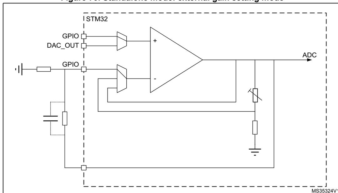
Standalone mode (external gain setting mode)
The procedure to use the OPAMP in standalone mode is presented below.
Starting from the default value of OPAMP_CSR, and the default state of GPIOx_MODER, configure bit OPA_RANGE according to the \( V_{DDA} \) voltage. As soon as the OPAEN bit is set, the two input pins and the output pin are connected to the operational amplifier.
This default configuration uses the factory trimming values and operates in normal mode (highest performance). The behavior of the OPAMP can be changed as follows:
- • OPALPM can be set to “operational amplifier low-power” mode in order to save power.
- • USERTRIM can be set to modify the trimming values for the input offset.
Figure 70. Standalone mode: external gain setting mode
Follower configuration mode
The procedure to use the OPAMP in follower mode is presented below.
- • Configure OPAMODE bits as “internal follower”.
- • Configure VP_SEL bits as “GPIO connected to VINP”.
- • As soon as the OPAEN bit is set, the signal on pin OPAMP_VINP is copied to pin OPAMP_VOUT.
Note: The pin corresponding to OPAMP_VINM is free for another usage.
Note: The signal on the operational amplifier output is also seen as an ADC input. As a consequence, the OPAMP configured in follower mode can be used to perform impedance adaptation on input signals before feeding them to the ADC input, assuming the input signal frequency is compatible with the operational amplifier gain bandwidth specification.
Figure 71. Follower configuration
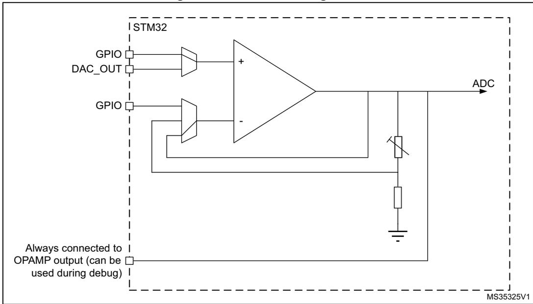
The diagram illustrates a follower configuration for an operational amplifier (OPAMP) within an STM32 microcontroller. The microcontroller is represented by a dashed box labeled 'STM32'. Inside, the non-inverting input (+) of the OPAMP is connected to a 'DAC_OUT' pin through a buffer. The inverting input (-) is connected to the OPAMP's output in a unity-gain feedback loop. The output is connected to an 'ADC' and a circuit consisting of a variable resistor and a fixed resistor connected to ground. A debug pin, labeled 'Always connected to OPAMP output (can be used during debug)', is also connected to the output. The diagram is labeled 'MS35325V1' in the bottom right corner.
Programmable Gain Amplifier mode
The procedure to use the OPAMP to amplify the amplitude of an input signal is presented below.
- • Configure OPAMODE bits as “internal PGA enabled”.
- • Configure PGA_GAIN bits as “internal PGA Gain 2, 4, 8 or 16”.
- • Configure VM_SEL bits as “inverting not externally connected”.
- • Configure VP_SEL bits as “GPIO connected to VINP”.
As soon as the OPAEN bit is set, the selected gain amplifies the signal on the OPAMP_VINP pin. This is visible on the OPAMP_VOUT pin.
Note: To avoid saturation, the input voltage should stay below \( V_{DDA} \) divided by the selected gain.
Figure 72. PGA mode, internal gain setting (x2/x4/x8/x16), inverting input not used
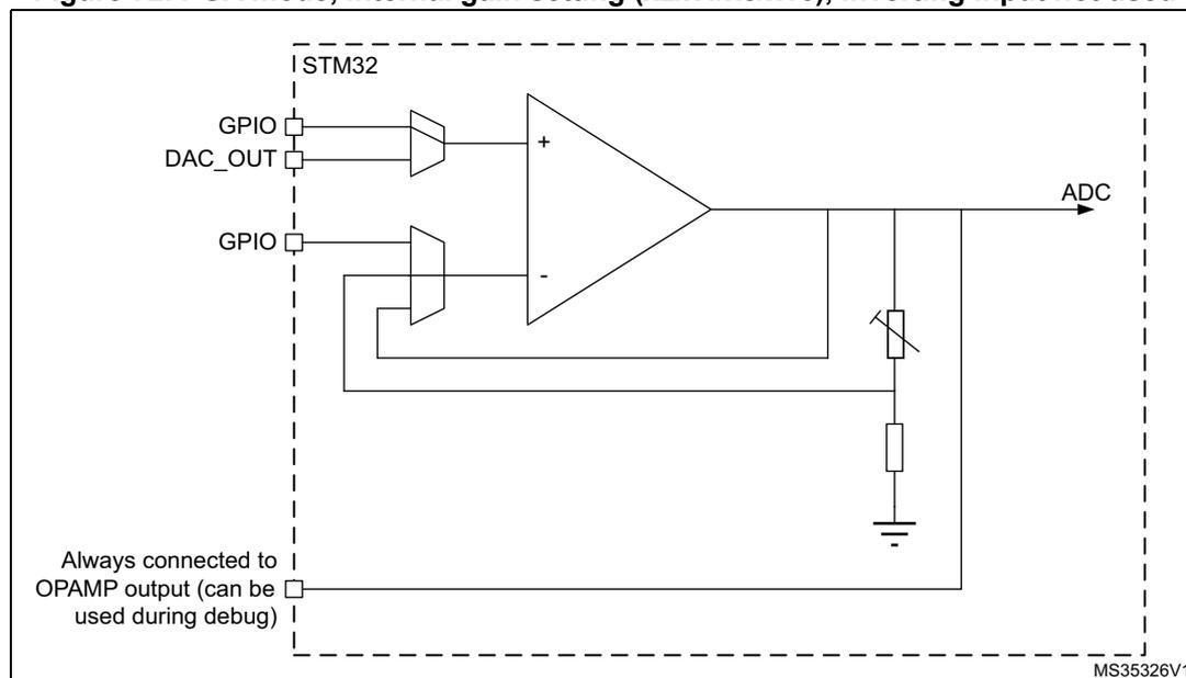
The diagram illustrates the internal configuration of an OPAMP within an STM32 microcontroller for PGA mode. The non-inverting input (+) is connected to a GPIO pin and a DAC_OUT pin. The inverting input (-) is connected to the output in a unity-gain feedback configuration. The output is connected to an ADC and a variable resistor (potentiometer) which is also connected to ground. A note indicates that the output is 'Always connected to OPAMP output (can be used during debug)'. The diagram is labeled MS35326V1.
Programmable Gain Amplifier mode with external filtering
The procedure to use the OPAMP to amplify the amplitude of an input signal, with an external filtering, is presented below.
- • Configure OPAMODE bits as “internal PGA enabled”.
- • Configure PGA_GAIN bits as “internal PGA Gain 2, 4, 8 or 16”.
- • Configure VM_SEL bits as “GPIO connected to VINM”.
- • Configure VP_SEL bits as “GPIO connected to VINP”.
Any external connection on VINP can be used in parallel with the internal PGA, for example a capacitor can be connected between VOUT and VINM for filtering purposes. See datasheet for the value of resistors used in the PGA resistor network.
Figure 73. PGA mode, internal gain setting (x2/x4/x8/x16), inverting input used for filtering
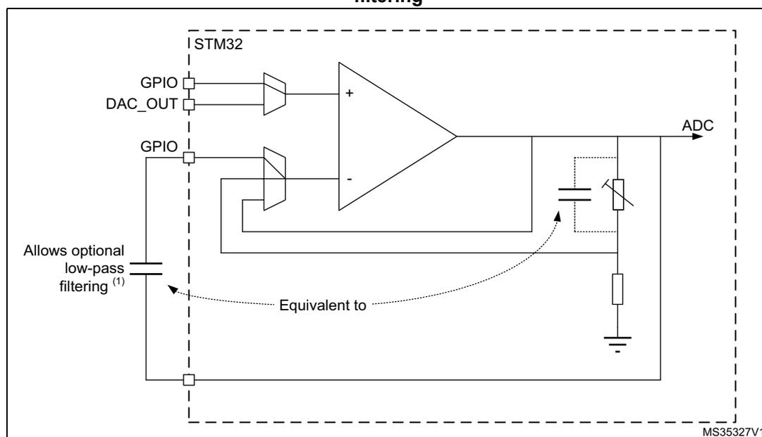
1. The gain depends on the cutoff frequency.
18.3.5 Calibration
At startup, the trimming values are initialized with the preset ‘factory’ trimming value.
The user can trim the operational amplifier offset. Specific registers allow different trimming values for normal mode and for low-power mode.
The aim of the calibration is to cancel as much as possible the OPAMP inputs offset voltage. The calibration circuitry reduces the inputs offset voltage to less than \( \pm 1.5 \) mV within stable voltage and temperature conditions.
For each mode of the operational amplifier, two trimming values need to be trimmed, one for N differential pair and one for P differential pair.
There are two registers for trimming the operational amplifier offset, one for normal mode ( OPAMP_OTR ) and one low-power mode ( OPAMP_LPOTR ). Each register is composed of five bits for P differential pair trimming, and five bits for N differential pair trimming. These are the ‘user’ values.
Using the USERTRIM bit in the OPAMP_CSR register, the user can switch from 'factory' values to 'user' trimmed values. This bit is reset at startup. The 'factory' value is then applied by default to the OPAMP trimming registers.
User is liable to change the trimming values in calibration or in functional mode.
The offset trimming registers are typically configured after the calibration operation is initialized by setting bit CALON to 1. When CALON = 1 the inputs of the operational amplifier are disconnected from the functional environment.
- • Setting CALSEL to 1 initializes the offset calibration for the P differential pair (low voltage reference used).
- • Resetting CALSEL to 0 initializes the offset calibration for the N differential pair (high voltage reference used).
When CALON = 1, the CALOUT bit reflects the influence of the trimming value selected by CALSEL and OPALPM. When the value of CALOUT switches between two consecutive trimming values, this means that those two values are the best trimming values. The CALOUT flag needs up to 1 ms after the trimming value is changed to become steady (see \( t_{OFFTRIMmax} \) delay specification in the electrical characteristics section of the datasheet).
Note: The closer the trimming value is to the optimum trimming value, the longer it takes to stabilize. The maximum stabilization time remains below 1 ms in any case.
Table 97. Operating modes and calibration
| Mode | Control bits | Output | ||||
|---|---|---|---|---|---|---|
| OPAEN | OPALPM | CALON | CALSEL | V OUT | CALOUT flag | |
| Normal operating mode | 1 | 0 | 0 | X | analog | 0 |
| Low-power mode | 1 | 1 | 0 | X | analog | 0 |
| Power down | 0 | X | X | X | Z | 0 |
| Offset cal high for normal mode | 1 | 0 | 1 | 0 | analog | X |
| Offset cal low for normal mode | 1 | 0 | 1 | 1 | analog | X |
| Offset cal high for low-power mode | 1 | 1 | 1 | 0 | analog | X |
| Offset cal low for low-power mode | 1 | 1 | 1 | 1 | analog | X |
Calibration procedure
Here are the steps to perform full operational amplifier calibration:
- 1. Select correct OPA_RANGE in OPAMP_CSR, then set the OPAEN bit in OPAMP_CSR to 1 to enable the operational amplifier.
- 2. Set the USERTRIM bit in the OPAMP_CSR register to 1.
- 3. Choose a calibration mode (refer to
Table 97: Operating modes and calibration
). The steps 3 to 4 must be repeated four times. For the first iteration, select :
- – Normal mode, offset cal high (N differential pair)
- 4. Increment TRIMOFFSETN[4:0] in OPAMP_OTR, starting from 00000b and until CALOUT changes to 1 in OPAMP_CSR.
Note: CALOUT switches from 0 to 1 for offset cal high and from 1 to 0 for offset cal low.
Note: Between the write to the OPAMP_OTR register and the read of the CALOUT value, make sure to wait for the \( t_{OFFTRIM}max \) delay specified in the electrical characteristics section of the datasheet, to get the correct CALOUT value.
The commutation means that the offset is correctly compensated and that the corresponding trim code must be saved in the OPAMP_OTR register.
Repeat steps 3 to 4 for:
- – Normal_mode and offset cal low
- – Low power mode and offset cal high
- – Low power mode and offset cal low
If a mode is not in use, you do not need to perform the corresponding calibration.
Note: During the whole calibration phase the external connection of the operational amplifier output must not pull up or down currents higher than 500 \( \mu \) A.
During the calibration procedure, it is necessary to set up OPAMODE bits as 00 or 01 (PGA disable) or 11 (internal follower).
18.4 OPAMP low-power modes
Table 98. Effect of low-power modes on the OPAMP
| Mode | Description |
|---|---|
| Sleep | No effect. |
| Stop 0 / Stop 1 | No effect, OPAMP registers content is kept. |
| Stop 2 | OPAMP registers content is kept. OPAMP must be disabled before entering Stop 2 mode. |
| Standby | The OPAMP registers are powered down and must be re-initialized after exiting Standby or Shutdown mode. |
| Shutdown |
18.5 OPAMP registers
18.5.1 OPAMP1 control/status register (OPAMP1_CSR)
Address offset: 0x00
Reset value: 0x0000 0000
| 31 | 30 | 29 | 28 | 27 | 26 | 25 | 24 | 23 | 22 | 21 | 20 | 19 | 18 | 17 | 16 |
|---|---|---|---|---|---|---|---|---|---|---|---|---|---|---|---|
| OPA_ RANGE | Res. | Res. | Res. | Res. | Res. | Res. | Res. | Res. | Res. | Res. | Res. | Res. | Res. | Res. | Res. |
| rw |
| 15 | 14 | 13 | 12 | 11 | 10 | 9 | 8 | 7 | 6 | 5 | 4 | 3 | 2 | 1 | 0 |
|---|---|---|---|---|---|---|---|---|---|---|---|---|---|---|---|
| CAL OUT | USER TRIM | CAL SEL | CALON | Res. | VP_ SEL | VM_SEL[9:8] | Res. | Res. | PGA_GAIN[5:4] | OPAMODE[3:2] | OPA LPM | OPAEN | |||
| r | rw | rw | rw | rw | rw | rw | rw | rw | rw | w | rw | rw | |||
Bit 31 OPA_RANGE : Operational amplifier power supply range for stability
All AOP must be in power down to allow AOP-RANGE bit write. It applies to all AOP embedded in the product.
0: Low range ( \( V_{DDA} < 2.4V \) )
1: High range ( \( V_{DDA} > 2.4V \) )
Bits 30:16 Reserved, must be kept at reset value.
Bit 15 CALOUT : Operational amplifier calibration output
During calibration mode offset is trimmed when this signal toggle.
Bit 14 USERTRIM : allows to switch from 'factory' AOP offset trimmed values to AOP offset 'user' trimmed values
This bit is active for both mode normal and low-power.
0: 'factory' trim code used
1: 'user' trim code used
Bit 13 CALSEL : Calibration selection
0: NMOS calibration (200mV applied on OPAMP inputs)
1: PMOS calibration ( \( V_{DDA}-200mV \) applied on OPAMP inputs)
Bit 12 CALON : Calibration mode enabled
0: Normal mode
1: Calibration mode (all switches opened by HW)
Bit 11 Reserved, must be kept at reset value.
Bit 10 VP_SEL : Non inverted input selection
0: GPIO connected to VINP
1: DAC connected to VINP
Bits 9:8 VM_SEL[9:8] : Inverting input selection
These bits are used only when OPAMODE = 00, 01 or 10.
00: GPIO connected to VINM (valid also in PGA mode for filtering)
01: Reserved
1x: Inverting input not externally connected. These configurations are valid only when OPAMODE = 10 (PGA mode)
Bits 7:6 Reserved, must be kept at reset value.
Bits 5:4 PGA_GAIN[5:4] : Operational amplifier Programmable amplifier gain value
- 00: internal PGA Gain 2
- 01: internal PGA Gain 4
- 10: internal PGA Gain 8
- 11: internal PGA Gain 16
Bits 3:2 OPAMODE[3:2] : Operational amplifier PGA mode
- 00: internal PGA disable
- 01: internal PGA disable
- 10: internal PGA enable, gain programmed in PGA_GAIN
- 11: internal follower
Bit 1 OPALPM : Operational amplifier Low Power Mode
The operational amplifier must be disable to change this configuration.
- 0: operational amplifier in normal mode
- 1: operational amplifier in low-power mode
Bit 0 OPAEN : Operational amplifier Enable
- 0: operational amplifier disabled
- 1: operational amplifier enabled
18.5.2 OPAMP1 offset trimming register in normal mode (OPAMP1_OTR)
Address offset: 0x04
Reset value: 0x0000 XXXX (factory trimmed values)
| 31 | 30 | 29 | 28 | 27 | 26 | 25 | 24 | 23 | 22 | 21 | 20 | 19 | 18 | 17 | 16 |
|---|---|---|---|---|---|---|---|---|---|---|---|---|---|---|---|
| Res. | Res. | Res. | Res. | Res. | Res. | Res. | Res. | Res. | Res. | Res. | Res. | Res. | Res. | Res. | Res. |
| 15 | 14 | 13 | 12 | 11 | 10 | 9 | 8 | 7 | 6 | 5 | 4 | 3 | 2 | 1 | 0 |
| Res. | Res. | Res. | TRIMOFFSETP[12:8] | Res. | Res. | Res. | TRIMOFFSETN[4:0] | ||||||||
| rw | rw | rw | rw | rw | rw | rw | rw | rw | rw | ||||||
Bits 31:13 Reserved, must be kept at reset value.
Bits 12:8 TRIMOFFSETP[12:8] : Trim for PMOS differential pairs
Bits 7:5 Reserved, must be kept at reset value.
Bits 4:0 TRIMOFFSETN[4:0] : Trim for NMOS differential pairs
18.5.3 OPAMP1 offset trimming register in low-power mode (OPAMP1_LPOTR)
Address offset: 0x08
Reset value: 0x0000 XXXX (factory trimmed values)
| 31 | 30 | 29 | 28 | 27 | 26 | 25 | 24 | 23 | 22 | 21 | 20 | 19 | 18 | 17 | 16 |
|---|---|---|---|---|---|---|---|---|---|---|---|---|---|---|---|
| Res. | Res. | Res. | Res. | Res. | Res. | Res. | Res. | Res. | Res. | Res. | Res. | Res. | Res. | Res. | Res. |
| 15 | 14 | 13 | 12 | 11 | 10 | 9 | 8 | 7 | 6 | 5 | 4 | 3 | 2 | 1 | 0 |
| Res. | Res. | Res. | TRIMLPOFFSETP[12:8] | Res. | Res. | Res. | TRIMLPOFFSETN[4:0] | ||||||||
| rw | rw | rw | rw | rw | rw | rw | rw | rw | rw | ||||||
Bits 31:13 Reserved, must be kept at reset value.
Bits 12:8 TRIMLPOFFSETP[12:8] : Low-power mode trim for PMOS differential pairs
Bits 7:5 Reserved, must be kept at reset value.
Bits 4:0 TRIMLPOFFSETN[4:0] : Low-power mode trim for NMOS differential pairs
18.5.4 OPAMP register map
Table 99. OPAMP register map and reset values
| Offset | Register | 31 | 30 | 29 | 28 | 27 | 26 | 25 | 24 | 23 | 22 | 21 | 20 | 19 | 18 | 17 | 16 | 15 | 14 | 13 | 12 | 11 | 10 | 9 | 8 | 7 | 6 | 5 | 4 | 3 | 2 | 1 | 0 |
|---|---|---|---|---|---|---|---|---|---|---|---|---|---|---|---|---|---|---|---|---|---|---|---|---|---|---|---|---|---|---|---|---|---|
| 0x00 | OPAMP1_CSR | OPA_RANGE | Res. | Res. | Res. | Res. | Res. | Res. | Res. | Res. | Res. | Res. | Res. | Res. | Res. | Res. | Res. | CALOUT | USERTRIM | CALSEL | CALON | Res. | VP_SEL | VM_SEL | Res. | Res. | Res. | PGA_GAIN | OPAMODE | OPALPM | OPAEN | ||
| Reset value | 0 | 0 | 0 | 0 | 0 | 0 | 0 | 0 | 0 | 0 | 0 | 0 | 0 | ||||||||||||||||||||
| 0x04 | OPAMP1_OTR | Res. | Res. | Res. | Res. | Res. | Res. | Res. | Res. | Res. | Res. | Res. | Res. | Res. | Res. | Res. | Res. | Res. | Res. | Res. | TRIM OFFSETP[4:0] | Res. | Res. | Res. | TRIM OFFSETN[4:0] | ||||||||
| Reset value | (1) | (1) | |||||||||||||||||||||||||||||||
| 0x08 | OPAMP1_LPOTR | Res. | Res. | Res. | Res. | Res. | Res. | Res. | Res. | Res. | Res. | Res. | Res. | Res. | Res. | Res. | Res. | Res. | Res. | Res. | TRIMLP OFFSETP[4:0] | Res. | Res. | Res. | TRIMLP OFFSETN[4:0] | ||||||||
| Reset value | (1) | (1) | |||||||||||||||||||||||||||||||
1. Factory trimmed values.
Refer to Section 2.2 on page 55 for the register boundary addresses.