3. Embedded flash memory (FLASH)
3.1 FLASH introduction
The flash memory interface manages CPU (Cortex®-M0+) AHB accesses to the flash memory. It implements erase and program flash memory operations, read and write protection, and security mechanisms.
The flash memory interface accelerates code execution with a system of instruction prefetch and cache lines.
3.2 FLASH main features
- • Up to 256 Kbytes of flash memory (main memory)
- • Memory organization:
- – Main memory block:
- Up to 32 Kbytes (4 Kbytes x 72 bits) on STM32U031xx devices
- Up to 256 Kbytes (32 bytes x 72 bits) on STM32U073xx and STM32U083xx devices
- – Information block:
- 32 Kbytes (4 Kwords x 72 bits)
- – Page size: 2 Kbytes
- – Main memory block:
- • 72-bit-wide data read (64 bits plus eight ECC bits)
- • Page erase (2 Kbytes) and mass erase
Flash memory interface features:
- • Flash memory read operations
- • Flash memory program/erase operations
- • Read protection activated by option (RDP)
- • Two write protection areas, selected by option (WRP)
- • Securable memory area
- • Flash memory empty check
- • Prefetch buffer
- • CPU instruction cache: 32 cache lines of 4 x 64 bits (1-Kbyte RAM)
- • Error code correction (ECC): eight bits for 64 bits
- • Option byte loader
3.3 FLASH functional description
3.3.1 Flash memory organization
The flash memory is organized as 72-bit-wide memory cells (64 bits plus eight ECC bits) that can be used for storing both code and data constants.
The flash memory is organized as follows:
- • Main memory block containing up to 128 pages of 2 Kbytes, each page with eight rows of 256 bytes
- • Information block containing:
- – System memory from which the CPU boots in system memory bootloader used to reprogram the flash memory through one of the following interfaces: USART, SPI, I2C, and USB. On the manufacturing line, the devices are programmed and protected against spurious write/erase operations. For further details, refer to the AN2606 available from www.st.com .
- – 1 Kbyte (128 double words) OTP (one-time programmable) for user data. The OTP data cannot be erased and can be written only once. Once written, the entire double word cannot be written anymore, even with the value 0x0000 0000 0000 0000.
- – Option bytes for user configuration.
The following table shows the mapping of the flash memory into information block and main memory area.
Table 7. Flash memory organization: information block
| Area | Addresses | Size (Kbytes) | Memory type |
|---|---|---|---|
| Information block | 0x1FFF 6C00 - 0x1FFF 7FFF | 5 | Non-user area |
| 0x1FFF 6800 - 0x1FFF 6BFF | 1 | OTP area | |
| 0x1FFF 0000 - 0x1FFF 67FF | 26 | System memory |
Table 8. Flash memory organization: main memory
| Area | Addresses | Size (Kbytes) | 64 Kbyte devices | 128 Kbyte devices | 256 Kbyte devices |
|---|---|---|---|---|---|
| Main memory | 0x0803 F800 - 0x0803 FFFF | 2 | - | - | Page 127 |
| ... | 2 | ... | |||
| 0x0802 0000 - 0x0802 7FFF | 2 | Page 64 | |||
| 0x0801 F800 - 0x0801 FFFF | 2 | Page 63 | |||
| ... | ... | - | ... | ||
| 0x0801 0000 - 0x0801 07FF | 2 | Page 32 | |||
| 0x0800 F800 - 0x0800 FFFF | 2 | Page 31 | |||
| ... | ... | ... | |||
| 0x0800 1000 - 0x0800 17FF | 2 | Page 2 | |||
| 0x0800 0800 - 0x0800 0FFF | 2 | Page 1 | |||
| 0x0800 0000 - 0x0800 07FF | 2 | Page 0 |
3.3.2 FLASH error code correction (ECC)
Data in flash memory words are 72-bits wide: eight bits are added per each double word (64 bits). The ECC mechanism supports:
- • One error detection and correction
- • Two errors detection
When one error is detected and corrected, the flag ECCC (ECC correction) is set in FLASH ECC register (FLASH_ECCR) . If ECCCIE is set, an interrupt is generated.
When two errors are detected, a flag ECCD (ECC detection) is set in FLASH ECC register (FLASH_ECCR) . In this case, an NMI is generated.
When an ECC error is detected, the address of the failing double word is saved in ADDR_ECC[16:0] bitfield of the FLASH_ECCR register. ADDR_ECC[2:0] are always cleared.
While ECCC or ECCD is set, FLASH_ECCR is not updated if a new ECC error occurs. FLASH_ECCR is updated only when ECC flags are cleared.
Note: For a virgin data: 0xFF FFFF FFFF FFFF FFFF, one error is detected and corrected, but two errors detection is not supported.
When an ECC error is reported, a new read at the failing address may not generate an ECC error if the data is still present in the current buffer, even if ECCC and ECCD are cleared. If this is not the desired behavior, the user must reset the cache.
3.3.3 FLASH read access latency
To correctly read data from flash memory, the number of wait states (LATENCY) must be correctly programmed in the FLASH access control register (FLASH_ACR) according to the frequency of the flash (HCLK) memory clock and the internal voltage range of the device V CORE . Refer to Section 4.1.6: Dynamic voltage scaling management . Table 9 shows the correspondence between wait states and flash memory clock frequency.
Table 9. Number of wait states according to flash memory clock (HCLK) frequency| Wait states (WS) (LATENCY) | HCLK (MHz) | |
|---|---|---|
| V CORE Range 1 | V CORE Range 2 | |
| 0 WS (1 CPU cycle) | ≤ 24 | ≤ 8 |
| 1 WS (2 CPU cycles) | ≤ 48 | ≤ 16 |
| 2 WS (3 CPU cycles) | ≤ 56 | ≤ 18 |
After power reset, the HCLK clock frequency is 16 MHz in Range 1 and 0 wait state (WS) is configured in the FLASH_ACR register.
When waking up from Standby, the HCLK clock frequency is 16 MHz in Range 1 and 0 wait state (WS) is configured in the FLASH_ACR register.
When changing the flash memory clock frequency or Range, the following software sequences must be applied in order to tune the number of wait states needed to access the flash memory:
Increasing the CPU frequency
- 1. Program the new number of wait states to the LATENCY bits of the FLASH access control register (FLASH_ACR) .
- 2. Check that the new number of wait states is taken into account to access the flash memory by reading back the LATENCY bits of the FLASH access control register (FLASH_ACR) , and wait until the programmed new number is read.
- 3. Modify the system clock source by writing the SW bits of the RCC_CFGR register.
- 4. If needed, modify the core clock prescaler by writing the HPRE bits of the RCC_CFGR register.
- 5. Optionally, check that the new system clock source or/and the new core clock prescaler value is/are taken into account by reading the clock source status (SWS bits) of the RCC_CFGR register, or/and the AHB prescaler value (HPREF bit), of the RCC_CFGR register.
Decreasing the CPU frequency
- 1. Modify the system clock source by writing the SW bits of the RCC_CFGR register.
- 2. If needed, modify the core clock prescaler by writing the HPRE bits of RCC_CFGR.
- 3. Check that the new system clock source or/and the new core clock prescaler value is/are taken into account by reading the clock source status (SWS bits) of the RCC_CFGR register, or/and the AHB prescaler value (HPREF bit), of the RCC_CFGR register, and wait until the programmed new system clock source or/and new flash memory clock prescaler value is/are read.
- 4. Program the new number of wait states to the LATENCY bits of the FLASH access control register (FLASH_ACR) .
- 5. Optionally, check that the new number of wait states is used to access the flash memory by reading back the LATENCY bits of the FLASH access control register (FLASH_ACR) .
3.3.4 Flash memory acceleration
Instruction prefetch
Each flash memory read operation provides 64 bits from either two instructions of 32 bits or four instructions of 16 bits according to the program launched. This 64-bits current instruction line is saved in a current buffer. So, in case of sequential code, at least two CPU cycles are needed to execute the previous read instruction line. Prefetch on the CPU S-bus can be used to read the next sequential instruction line from the flash memory while the current instruction line is being requested by the CPU.
Prefetch is enabled by setting the PRFTEN bit of the FLASH access control register (FLASH_ACR) . This feature is useful if at least one wait state is needed to access the flash memory.
When the code is not sequential (branch), the instruction may not be present in the currently used instruction line or in the prefetched instruction line. In this case (miss), the penalty in terms of number of cycles is at least equal to the number of wait states.
If a loop is present in the current buffer, no new access is performed.
Cache memory
To limit the time lost due to jumps, the STM32U0 microcontrollers feature 1 Kbytes of instruction cache memory. This feature can be enabled by setting the instruction cache enable (ICEN) bit of the FLASH access control register (FLASH_ACR) . Each time a miss occurs (requested data not present in the currently used instruction line, in the prefetched instruction line or in the instruction cache memory), the line read is copied into the instruction cache memory. If some data contained in the instruction cache memory are requested by the CPU, they are provided without inserting any delay. Once all the instruction cache memory lines are filled, the LRU (least recently used) policy is used to determine the line to replace in the instruction memory cache. This feature is particularly useful in case of code containing loops.
The instruction cache memory is enabled after system reset.
No data cache is available on Cortex ® -M0+.
3.3.5 FLASH program and erase operations
The device-embedded flash memory can be programmed using in-circuit programming or in-application programming.
The in-circuit programming (ICP) method is used to update the entire contents of the flash memory, using SWD protocol or the supported interfaces by the system bootloader, to load the user application for the CPU, into the microcontroller. ICP offers quick and efficient design iterations and eliminates unnecessary package handling or socketing of devices.
In contrast to the ICP method, in-application programming (IAP) can use any communication interface supported by the microcontroller (I/Os, UART, I 2 C, SPI, etc.) to download programming data into memory. IAP allows the user to reprogram the flash memory while the application is running. Nevertheless, part of the application has to have been previously programmed in the flash memory using ICP.
The success of a data word programming operation and a page/bank erase operation is not guaranteed if aborted due to device reset or power loss.
During a program/erase operation to the flash memory, any attempt to read the flash memory stalls the bus. The read operation proceeds correctly once the program/erase operation has completed.
Unlocking the flash memory
After reset, write into the FLASH control register (FLASH_CR) is not allowed so as to protect the flash memory against possible unwanted operations due, for example, to electric disturbances. The following sequence unlocks these registers:
- 1. Write KEY1 = 0x4567 0123 in the FLASH key register (FLASH_KEYR)
- 2. Write KEY2 = 0xCDEF 89AB in the FLASH key register (FLASH_KEYR) .
Any wrong sequence locks the FLASH_CR registers until the next system reset. In the case of a wrong key sequence, a bus error is detected and a Hard Fault interrupt is generated.
The FLASH_CR register can be locked again by software by setting the LOCK bit in one of these registers.
Note: The FLASH_CR register cannot be written when the BSY1 bit of the FLASH status register (FLASH_SR) is set. Any attempt to write to this register with the BSY1 bit set causes the AHB bus to stall until the BSY1 bit is cleared.
Caution: Due to the structure of the flash memory (64 bits of data associated to 8 bits of ECC), any ongoing memory operation that is interrupted by a physical event (such as a reset or a power off) may result in flash memory data corruption, and/or inconsistent ECC bits. The target address may trigger an ECC interrupt or an NMI when accessed later on. It is consequently important to always handle flash memory write/erase operations with care, and manage ECC events in the firmware.
3.3.6 FLASH main memory erase sequences
The flash memory erase operation can be performed at page level (page erase), or on the whole memory (mass erase). Mass erase does not affect the information block (system flash memory, OTP, and option bytes).
Flash memory page erase
When a page is protected by WRP, it is not erased and the WRPERR bit is set.
Table 10. Page erase overview
| HDP1_ACCDIS [7:0] | WRP | Comment | WRPERR | CPU bus error |
|---|---|---|---|---|
| 0xA3 | No | Page is erased | No | No |
| Yes | Page erase aborted (no page erase started) | Yes | ||
| Any value different from 0xA3 | X | Protected pages only | No | Yes |
To erase a page (2 Kbytes), proceed as follows:
- 1. Check that no flash memory operation is ongoing by checking the BSY1 bit of the FLASH status register (FLASH_SR) .
- 2. Check and clear all error programming flags due to a previous programming. If not, PGSERR is set.
- 3. Check that the CFGBSY bit of FLASH status register (FLASH_SR) is cleared.
- 4. Set the PER bit and select the page to erase (PNB) in the FLASH control register (FLASH_CR) .
- 5. Set the STRT bit of the FLASH control register (FLASH_CR) .
- 6. Wait until the CFGBSY bit of the FLASH status register (FLASH_SR) is cleared again.
Note: The HSI16 internal oscillator is automatically enabled when the STRT bit is set. It is automatically disabled when the STRT bit is cleared, except if previously enabled with the HSION bit of the RCC_CR register.
Flash memory bank or mass erase
When WRP is enabled, the flash memory mass erase is aborted, no erase starts, and the WRPERR bit is set.
Table 11. Mass erase overview
| HDP1_ACCDIS [7:0] | WRP | Comment | WRPERR | CPU bus error |
|---|---|---|---|---|
| 0xA3 | No | Memory is erased | No | No |
| Yes | Erase aborted (no erase started) | Yes | ||
| Any value different from 0xA3 | X | Erase aborted (no erase started) | No | Yes |
To perform a mass erase, proceed as follows:
- 1. Check that no flash memory operation is ongoing by checking the BSY1 bit of the FLASH status register (FLASH_SR) .
- 2. Check and clear all error programming flags due to a previous programming. If not, PGSERR is set.
- 3. Check that the CFGBSY bit of FLASH status register (FLASH_SR) is cleared.
- 4. Set the MER1 bit of the FLASH control register (FLASH_CR) .
- 5. Set the STRT bit of the FLASH control register (FLASH_CR) .
- 6. Wait until the CFGBSY bit of the FLASH status register (FLASH_SR) is cleared again.
Note: The HSI16 internal oscillator is automatically enabled when the STRT bit is set. It is automatically disabled when the STRT bit is cleared, except if previously enabled with the HSION bit of the RCC_CR register.
3.3.7 FLASH main memory programming sequences
The flash memory is programmed 72 bits (64 bits plus 8-bit ECC).
Programming a previously programmed address with a nonzero data is not allowed. Any such attempt sets PROGERR flag of the FLASH status register (FLASH_SR) .
It is only possible to program a double word (2 x 32-bit data).
- • Any attempt to write byte (8 bits) or half-word (16 bits) sets SIZERR flag of the FLASH status register (FLASH_SR) .
- • Any attempt to write a double word that is not aligned with a double word address sets PGAERR flag of the FLASH status register (FLASH_SR) .
Standard programming
The flash memory programming sequence in fast programming mode is as follows:
- 1. Check that no main flash memory operation is ongoing by checking the BSY1 bit of the FLASH status register (FLASH_SR) .
- 2. Check and clear all error programming flags due to a previous programming. If not, PGSERR is set.
- 3. Check that the CFGBSY bit of FLASH status register (FLASH_SR) is cleared.
- 4. Set the PG bit of the FLASH control register (FLASH_CR) .
- 5. Perform the data write operation at the desired memory address, inside main memory block or OTP area. Only double word (64 bits) can be programmed.
- a) Write a first word in an address aligned with double word.
- b) Write the second word.
- 6. Wait until the CFGBSY bit of the FLASH status register (FLASH_SR) is cleared again.
- 7. Check that the EOP flag in the FLASH status register (FLASH_SR) is set (programming operation succeeded), and clear it by software.
- 8. Clear the PG bit of the FLASH control register (FLASH_CR) if there no more programming request anymore.
Note: When the flash memory interface has received a good sequence (a double word), programming is automatically launched, and the BSY1 bit set.
The HSI16 internal oscillator is automatically enabled when the PG bit is set. It is automatically disabled when the PG bit is cleared, except if previously enabled with the HSION bit of the RCC_CR register.
Fast programming
The main purpose of this mode is to reduce the page programming time. It is achieved by eliminating the need for verifying the flash memory locations before they are programmed, thus saving the time of high voltage ramping and falling for each double word.
This mode allows programming a row (32 double words = 256 bytes).
During fast programming, the flash memory clock (HCLK) frequency must be at least 8 MHz.
Only the main memory can be programmed in Fast programming mode.
The main flash memory programming sequence in standard mode is described below:
- 1. Perform a mass or page erase. If not, PGSERR is set.
- 2. Check that no main flash memory operation is ongoing by checking the BSY1 bit of the FLASH status register (FLASH_SR) .
- 3. Check and clear all error programming flag due to a previous programming.
- 4. Check that the CFGBSY bit of FLASH status register (FLASH_SR) is cleared.
- 5. Set the FSTPG bit in FLASH control register (FLASH_CR) .
- 6. Write 32 double words to program a row (256 bytes).
- 7. Wait until the CFGBSY bit of the FLASH status register (FLASH_SR) is cleared again.
- 8. Check that the EOP flag in the FLASH status register (FLASH_SR) is set (programming operation succeeded), and clear it by software.
- 9. Clear the FSTPG bit of the FLASH status register (FLASH_SR) if there are no more programming requests anymore.
Note: When attempting to write in Fast programming mode while a read operation is ongoing, the programming is aborted without any system notification (no error flag is set).
When the flash memory interface has received the first double word, programming is automatically launched. The BSY1 bit is set when the high voltage is applied for the first double word, and it is cleared when the last double word has been programmed or in case of error.
The HSI48 internal oscillator (with a divide by three to provide 16 MHz) is automatically enabled when the FSTPG bit is set. It is automatically disabled when the FSTPG bit is cleared, except if previously enabled with the HSION bit of the RCC_CR register.
The 16 double words must be written successively. The high voltage is kept on the flash memory for all the programming. Maximum time between two double words write requests is the time programming (around 20 µs). If a second double word arrives after this time programming, fast programming is interrupted, and MISSERR is set.
High voltage must not exceed 8 ms for a full row between two erases. This is guaranteed by the sequence of 32 double words successively written with a clock system greater or equal to 8 MHz. An internal time-out counter counts 7 ms when Fast programming is set and stops the programming when time-out is over. In this case, the FASTERR bit is set.
If an error occurs, high voltage is stopped, and the next double word to programmed is not programmed. Anyway, all previous double words have been properly programmed.
Programming errors
Several kinds of errors can be detected. In case of error, the flash memory operation (programming or erasing) is aborted.
- • PROGERR: Programming error
In standard programming: PROGERR is set if the word to write is not previously erased (except if the value to program is full zero and the target address is in the main memory).
- • SIZERR: Size programming error
In standard programming or in fast programming: only double word can be programmed, and only 32-bit data can be written. SIZERR is set if a byte or an half-word is written.
- • PGAERR: Alignment programming error
PGAERR is set if one of the following conditions occurs:
- – In standard programming: the first word to be programmed is not aligned with a double word address, or the second word does not belong to the same double word address.
- – In fast programming: the data to program does not belong to the same row than the previous programmed double words, or the address to program is not greater than the previous one.
- •
PGSERR:
Programming sequence error
PGSERR is set if one of the following conditions occurs:
- – In the standard programming sequence or the fast programming sequence: a data is written when PG and FSTPG are cleared.
- – In the standard programming sequence or the fast programming sequence: MER1 and PER are not cleared when PG or FSTPG is set.
- – In the fast programming sequence: the Mass erase is not performed before setting the FSTPG bit.
- – In the mass erase sequence: PG, FSTPG, and PER are not cleared when MER1 is set.
- – In the page erase sequence: PG, FSTPG, and MER1 are not cleared when PER is set.
- – PGSERR is also set if PROGERR, SIZERR, PGAERR, WRPERR, MISSERR, FASTERR, or PGSERR is set due to a previous programming error.
- •
WRPERR:
Write protection error
WRPERR is set if one of the following conditions occurs:
- – Attempt to program or erase in a write protected area (WRP).
- – Attempt to perform a mass erase when one page or more is protected by WRP.
- – The debug features are connected or the boot is executed from SRAM or from system flash memory when the read protection (RDP) is set to level 1.
- – Attempt to modify the option bytes when the read protection (RDP) is set to level 2.
- •
MISSERR:
Fast programming data miss error
In fast programming: all the data must be written successively. MISSERR is set if the previous data programming is finished and the next data to program is not written yet.
- •
FASTERR:
Fast programming error
In fast programming: FASTERR is set if one of the following conditions occurs:
- – when FSTPG bit is set for more than 8 ms, which generates a time-out detection
- – when the row fast programming has been interrupted by a MISSERR, PGAERR, WRPERR, or SIZERR
- •
OPERR:
Generic error related to program/erase operations.
This flag can be set only if the error interrupt enable flag is set (ERRIE). In this case, it is set on any error condition (SEQERR, PROGERR, SIZERR, PGAERR, WRPERR,
MISSERR, PGSERR or FASTERR). Once set, it can only be cleared by programming it to 1.
- • OEMOPTWERR: Key setting error
This flag is set when an invalid configuration is programmed to the OEM keys. It is set when attempting:
- – to modify the OEM1KEYWxR registers when the RDP level 0 is disabled and the OEM1LOCK bit of the FLASH_SR is set.
- – to modify the OEM2KEYWxR registers when the RDP level 0 is disabled and the OEM2LOCK bit of the FLASH_SR is set.
- – to perform a regression from RDP level 1 to RDP level 0, while the OEM1LOCK bit of FLASH_SR is set and a wrong OEM1KEY is transmitted through JTAG or SWD.
- • HDOPTWERR: HDP setting error
This flag is set when an invalid configuration is programmed to the HDP option bytes. It is set when attempting:
- – to modify the HDP1EN[7:0] and/or the HDP1_PEND[6:0] bitfield of the FLASH_SECR register, when the HDP1_ACCDIS[7:0] and the HDP1EXT_ACCDIS[7:0] bitfields of the FLASH_HDPCR register are not equal to their reset value (0xA3).
- – to set the HDP1_ACCDIS[7:0] and/or the HDP1EXT_ACCDIS[7:0] bitfields to a value different from their reset value (0xA3), while the HDP1EN[7:0] and/or the HDP1_PEND[6:0] bitfields have been changed, and no option byte modification and loading (OPTSTRT and OBL_LAUNCH bits set in the FLASH_CR registers) has been done in between.
If an error occurs during a program or erase operation, one of the following error flags of the FLASH status register (FLASH_SR) is set:
- • PROGERR, SIZERR, PGAERR, PGSERR, MISSERR (program error flags)
- • WRPERR (protection error flag)
In this case, if the error interrupt enable bit ERRIE of the FLASH control register (FLASH_CR) is set, an interrupt is generated and the operation error flag OPERR of the FLASH status register (FLASH_SR) is set.
Note: If several successive errors are detected (for example, in case of DMA transfer to the flash memory), the error flags cannot be cleared until the end of the successive write request.
Programming and cache
If an erase operation in flash memory also concerns data in the instruction cache, the user has to ensure that these data are rewritten before they are accessed during code execution.
Note: The cache should be flushed only when it is disabled (ICEN = 0).
3.4 FLASH option bytes
3.4.1 FLASH option byte description
The option bytes are configured by the end user depending on the application requirements. As a configuration example, the watchdog may be selected in hardware or software mode (refer to Section 3.4.2: FLASH option byte programming ).
A double word is split up in option bytes as indicated in Table 12 .
Table 12. Option byte format
| 63-56 | 55-48 | 47-40 | 39-32 | 31-24 | 23-16 | 15-8 | 7-0 |
|---|---|---|---|---|---|---|---|
| Complemented option byte 3 | Complemented option byte 2 | Complemented option byte 1 | Complemented option byte 0 | Option byte 3 | Option byte 2 | Option byte 1 | Option byte 0 |
Table 13 shows the organization of the option bytes (the lower word only) in the flash memory information block. The software can read the option bytes from these flash memory locations or from their corresponding option registers referenced in the table. Refer to sections FLASH option register (FLASH_OPTR) to FLASH security register (FLASH_SECR) for the description of the option register bitfields, also applicable to the option byte bitfields.
Table 13. Organization of option bytes
| Corresponding option register (section) | 31 | 30 | 29 | 28 | 27 | 26 | 25 | 24 | 23 | 22 | 21 | 20 | 19 | 18 | 17 | 16 | 15 | 14 | 13 | 12 | 11 | 10 | 9 | 8 | 7 | 6 | 5 | 4 | 3 | 2 | 1 | 0 | ||||||
|---|---|---|---|---|---|---|---|---|---|---|---|---|---|---|---|---|---|---|---|---|---|---|---|---|---|---|---|---|---|---|---|---|---|---|---|---|---|---|
| Option byte 3 | Option byte 2 | Option byte 1 | Option byte 0 | |||||||||||||||||||||||||||||||||||
| FLASH_OPTR (Section 3.7.7) | Reserved | IRHEN | NRST_MODE[1:0] | NBOOT0 | NBOOT1 | NBOOT_SEL | BKPSRAM_HW_ERASE_DISABLE | RAM_PARITY_CHECK | BDRST | Reserved | WWDG_SW | IWDG_STBY | IWDG_STOP | IWDG_SW | NRST_SHDW | NRST_STDBY | NRST_STOP | Reserved | BOR_LEV[1:0] | BOR_EN | RDP[7:0] | |||||||||||||||||
| Factory value | X | X | 1 | 1 | 1 | 1 | 1 | 1 | 1 | 1 | 1 | X | 1 | 1 | 1 | 1 | 1 | 1 | X | X | 1 | 1 | 1 | 1 | 1 | 0 | 1 | 0 | 1 | 0 | 1 | 0 | ||||||
| FLASH_WRP1AR (Section 3.7.8) | Reserved | WRP1A_END [6:0] | Reserved | WRP1A_STRT [6:0] | ||||||||||||||||||||||||||||||||||
| Factory value | X | X | X | X | X | X | X | X | 0 | 0 | 0 | 0 | 0 | 0 | 0 | 0 | X | X | X | X | X | X | X | X | X | 1 | 1 | 1 | 1 | 1 | 1 | 1 | 1 | |||||
| FLASH_WRP1BR (Section 3.7.9) | Reserved | WRP1B_END [6:0] | Reserved | WRP1B_STRT [6:0] | ||||||||||||||||||||||||||||||||||
| Factory value | X | X | X | X | X | X | X | X | 0 | 0 | 0 | 0 | 0 | 0 | 0 | 0 | X | X | X | X | X | X | X | X | X | 1 | 1 | 1 | 1 | 1 | 1 | 1 | 1 | |||||
Table 13. Organization of option bytes (continued)
| Corresponding option register (section) | 31 | 30 | 29 | 28 | 27 | 26 | 25 | 24 | 23 | 22 | 21 | 20 | 19 | 18 | 17 | 16 | 15 | 14 | 13 | 12 | 11 | 10 | 9 | 8 | 7 | 6 | 5 | 4 | 3 | 2 | 1 | 0 |
|---|---|---|---|---|---|---|---|---|---|---|---|---|---|---|---|---|---|---|---|---|---|---|---|---|---|---|---|---|---|---|---|---|
| Option byte 3 | Option byte 2 | Option byte 1 | Option byte 0 | |||||||||||||||||||||||||||||
| FLASH_SECR (Section 3.7.10) | HDP1EN[7:0] | Reserved | Reserved | HDP1_PEND [6:0] | ||||||||||||||||||||||||||||
| Factory value | 1 | 0 | 1 | 1 | 0 | 1 | 0 | 0 | X | X | X | X | X | X | X | X | 0 | X | X | X | X | X | X | X | X | 0 | 0 | 0 | 0 | 0 | 0 | 0 |
| Reserved | ||||||||||||||||||||||||||||||||
| FLASH_OEM1KEYR1 | OEM1KEY[31:0] | |||||||||||||||||||||||||||||||
| Factory value | 1 | 1 | 1 | 1 | 1 | 1 | 1 | 1 | 1 | 1 | 1 | 1 | 1 | 1 | 1 | 1 | 1 | 1 | 1 | 1 | 1 | 1 | 1 | 1 | 1 | 1 | 1 | 1 | 1 | 1 | 1 | 1 |
| FLASH_OEM1KEYR2 | OEM1KEY[63:32] | |||||||||||||||||||||||||||||||
| Factory value | 1 | 1 | 1 | 1 | 1 | 1 | 1 | 1 | 1 | 1 | 1 | 1 | 1 | 1 | 1 | 1 | 1 | 1 | 1 | 1 | 1 | 1 | 1 | 1 | 1 | 1 | 1 | 1 | 1 | 1 | 1 | 1 |
| FLASH_OEM1KEYR3 | OEM1KEY[95:64] | |||||||||||||||||||||||||||||||
| Factory value | 1 | 1 | 1 | 1 | 1 | 1 | 1 | 1 | 1 | 1 | 1 | 1 | 1 | 1 | 1 | 1 | 1 | 1 | 1 | 1 | 1 | 1 | 1 | 1 | 1 | 1 | 1 | 1 | 1 | 1 | 1 | 1 |
| FLASH_OEM1KEYR4 | OEM1KEY[127:96] | |||||||||||||||||||||||||||||||
| Factory value | 1 | 1 | 1 | 1 | 1 | 1 | 1 | 1 | 1 | 1 | 1 | 1 | 1 | 1 | 1 | 1 | 1 | 1 | 1 | 1 | 1 | 1 | 1 | 1 | 1 | 1 | 1 | 1 | 1 | 1 | 1 | 1 |
| FLASH_OEM2KEYR1 | OEM2KEY[31:0] | |||||||||||||||||||||||||||||||
| Factory value | 1 | 1 | 1 | 1 | 1 | 1 | 1 | 1 | 1 | 1 | 1 | 1 | 1 | 1 | 1 | 1 | 1 | 1 | 1 | 1 | 1 | 1 | 1 | 1 | 1 | 1 | 1 | 1 | 1 | 1 | 1 | 1 |
| FLASH_OEM2KEYR2 | OEM2KEY[63:32] | |||||||||||||||||||||||||||||||
| Factory value | 1 | 1 | 1 | 1 | 1 | 1 | 1 | 1 | 1 | 1 | 1 | 1 | 1 | 1 | 1 | 1 | 1 | 1 | 1 | 1 | 1 | 1 | 1 | 1 | 1 | 1 | 1 | 1 | 1 | 1 | 1 | 1 |
| FLASH_OEM2KEYR3 | OEM2KEY[95:64] | |||||||||||||||||||||||||||||||
| Factory value | 1 | 1 | 1 | 1 | 1 | 1 | 1 | 1 | 1 | 1 | 1 | 1 | 1 | 1 | 1 | 1 | 1 | 1 | 1 | 1 | 1 | 1 | 1 | 1 | 1 | 1 | 1 | 1 | 1 | 1 | 1 | 1 |
| FLASH_OEM2KEYR4 | OEM2KEY[127:96] | |||||||||||||||||||||||||||||||
| Factory value | 1 | 1 | 1 | 1 | 1 | 1 | 1 | 1 | 1 | 1 | 1 | 1 | 1 | 1 | 1 | 1 | 1 | 1 | 1 | 1 | 1 | 1 | 1 | 1 | 1 | 1 | 1 | 1 | 1 | 1 | 1 | 1 |
3.4.2 FLASH option byte programming
After reset, the option related bits of the FLASH control register (FLASH_CR) are write-protected. To run any operation on the option byte page, the option lock bit OPTLOCK of the FLASH control register (FLASH_CR) must be cleared. The following sequence is used to unlock this register:
- 1. Unlock the FLASH_CR with the LOCK clearing sequence (refer to Unlocking the flash memory ).
- 2. Write OPTKEY1 = 0x0819 2A3B of the FLASH option key register (FLASH_OPTKEYR) .
- 3. Write OPTKEY2 = 0x4C5D 6E7F of the FLASH option key register (FLASH_OPTKEYR) .
Any wrong sequence locks up the flash memory option registers until the next system reset. In the case of a wrong key sequence, a bus error is detected and a Hard Fault interrupt is generated.
The user options can be protected against unwanted erase/program operations by setting the OPTLOCK bit by software.
Note: If LOCK is set by software, OPTLOCK is automatically set as well.
Modifying user options
The option bytes are programmed differently from a main memory user address.
To modify the value of user options, follow the procedure below:
- 1. Clear OPTLOCK option lock bit with the clearing sequence described above
- 2. Write the desired values in the FLASH option registers.
- 3. Check that no flash memory operation is ongoing, by checking the BSY1 bit of the FLASH status register (FLASH_SR) .
- 4. Set the options start bit OPTSTRT of the FLASH control register (FLASH_CR) .
- 5. Wait for the BSY1 bit to be cleared.
Note: Any modification of the value of one option is automatically performed by erasing user option byte pages first, and then programming all the option bytes with the values contained in the flash memory option registers.
The complementary values are automatically computed and written into the complemented option bytes upon setting the OPTSTRT bit.
Caution: Upon an option byte programming failure (for any reason, such as loss of power or a reset during the option byte change sequence), the mismatch values of the option bytes are loaded after reset. Those mismatch values force a secure configuration that might permanently lock the device. To prevent this, only program option bytes in a safe environment-safe supply, no pending watchdog, and clean reset line.
Option byte loading
After the BSY1 bit is cleared, all new options are updated into the flash memory, but not applied to the system. A read from the option registers still returns the last loaded option byte values. The new options has effect on the system only after they are loaded.
Option byte loading is performed in two cases:
- • when OBL_LAUNCH bit of the FLASH control register (FLASH_CR) is set
- • after a power reset (BOR reset or exit from Standby/Shutdown modes)
Option byte loader performs a read of the options block and stores the data into internal option registers. These internal registers configure the system and can be read by software. Setting OBL_LAUNCH generates a reset so the option byte loading is performed under system reset.
Each option bit has also its complement in the same double word. During option loading, a verification of the option bit and its complement allows to check that the loading has correctly taken place.
During option byte loading, the options are read by double word.
If the word and its complement are matching, the option word/byte is copied into the option register.
If the comparison between the word and its complement fails, a status bit OPTVERR is set. Mismatch values are forced into the option registers:
- • For USR OPT option, the value of mismatch is 1 for all option bits.
- • For WRP option, the value of mismatch is the default value “No protection”.
- • For RDP option, the value of mismatch is the default value “level 1”.
- • For BOOT_LOCK, the value of mismatch is “boot forced from main flash memory”.
Upon system reset, the option bytes are copied into the following option registers that can be read and written by software:
- • FLASH_OPTR
- • FLASH_WRP1xR (x = A or B)
- • FLASH_SECR
These registers are also used to modify options. If these registers are not modified by user, they reflect the options states of the system. See Section : Modifying user options for more details.
3.5 Flash memory protection
The main flash memory can be protected against external accesses with the read protection (RDP). The pages can also be protected against unwanted write (WRP) due to loss of program counter context. The write-protection WRP granularity is 2 Kbytes. Apart from the RDP and WRP, the flash memory also features an HDP securable area.
3.5.1 FLASH read protection (RDP)
The read protection is activated by setting the RDP option byte and then, by performing an option byte loading (OBL) to reload the new RDP option byte. The read protection protects the main flash memory, the option bytes, and the backup registers.
When the read protection is set during or after (since last power on), the debugger is connected or the MCU boot from the system memory/SRAM, apply a POR (power-on reset) instead of a system reset. Otherwise, any data read triggers a hard fault.
Note: If the read protection is programmed through software, do not set the OBL_LAUNCH bit (FLASH control register (FLASH_CR) register) to reload the option byte. Instead, perform a POR. This can be done by entering Standby or Shutdown mode then waking up the device
There are three levels of read protection from no protection (level 0) to maximum protection or no debug (level 2).
The flash memory is protected when the RDP option byte and its complement contain the pair of values shown in Table 14 .
Table 14. Flash memory read protection status
| RDP byte value | RDP complement byte value | Read protection level |
|---|---|---|
| 0xAA | 0x55 | Level 0 |
| Any values except the combinations [0xAA, 0x55] and [0xCC, 0x33] | Level 1 (default) | |
| 0xCC | 0x33 | Level 2 |
The system memory area is read-accessible whatever the protection level. It is never accessible for program/erase operation.
Level 0: no protection
Read, program, and erase operations within the main flash memory area are possible. The option bytes are also accessible by all operations.
Level 1: Read protection
Level 1 read protection is set when the RDP byte and the RDP complemented byte contain any value combinations other than [0xAA, 0x55] and [0xCC, 0x33]. Level 1 is the default protection level when RDP option byte is erased.
- • User mode: Code executing in user mode (boot from user flash memory) can access main flash memory and option bytes with all operations.
- • Debug, boot from SRAM, and boot from system memory modes: In debug mode or when code boots from SRAM or system memory, the main flash memory is totally inaccessible. In these modes, a read or write access to the flash memory generates a bus error and a Hard Fault interrupt.
Level 2: No debug
In this level, the protection level 1 is guaranteed. In addition, the CPU debug port, the boot from RAM (boot RAM mode) and the boot from system memory (bootloader mode) are no more available. In user execution mode (boot FLASH mode), all operations are allowed on the main flash memory.
Note: The CPU debug port is also disabled under reset.
STMicroelectronics is not able to perform analysis on defective parts on which the level 2 protection has been set.
Changing the read protection level
The read protection level can change:
- • from level 0 to level 1, upon changing the value of the RDP byte to any value except 0xCC
- • from level 0 or level 1 to level 2, upon changing the value of the RDP byte to 0xCC
- • from level 1 to level 0, upon changing the value of the RDP byte to 0xAA
Once in level 2, it is no more possible to modify the read protection level.
The OTP area is not affected by a mass erase and remains unchanged.
Note: Mass erase (full or partial) is only triggered by the RDP regression from level 1 to level 0. RDP level increase (level 0 to level 1, 1 to 2, or 0 to 2) does not cause any mass erase.
To validate the protection level change, the option bytes must be reloaded by setting the OBL_LAUNCH bit of the FLASH control register (FLASH_CR) .
Figure 3. Changing read protection (RDP) level
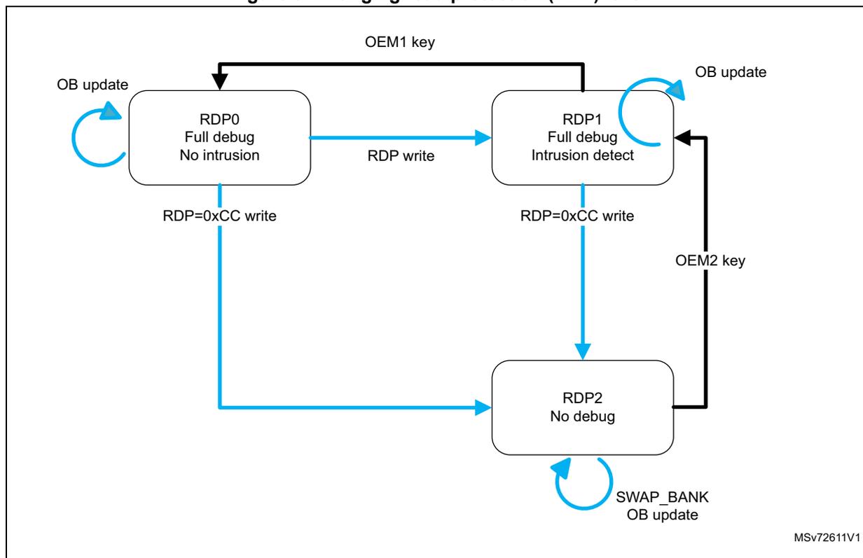
The diagram illustrates the transitions between three read protection (RDP) levels:
- RDP0 : Full debug, No intrusion. This is the initial state. It can be changed to RDP1 via an 'RDP write' or to RDP2 via an 'RDP=0xCC write'. An 'OB update' is also associated with this state.
- RDP1 : Full debug, Intrusion detect. This state is reached from RDP0. It can be changed to RDP2 via an 'RDP=0xCC write'. An 'OB update' is associated with this state. A transition back to RDP0 is triggered by the 'OEM1 key'.
- RDP2 : No debug. This state is reached from RDP0 or RDP1. An 'OB update' is associated with this state. A transition back to RDP0 is triggered by the 'OEM2 key'.
Additional transitions shown include 'SWAP_BANK OB update' leading to RDP2 from below, and 'OB update' leading to RDP0 from the left.
Table 15. Access status versus protection level and execution modes
| Area | Protection level | User execution (Boot from flash) | Debug/ Boot from RAM/ Boot from loader | ||||
|---|---|---|---|---|---|---|---|
| Read | Write | Erase | Read | Write | Erase | ||
| Main flash memory | 1 | Yes | Yes | Yes | No | No | No (3) |
| 2 | Yes | Yes | Yes | N/A (1) | N/A (1) | N/A (1) | |
| System memory (2) | 1 | Yes | No | No | Yes | No | No |
| 2 | Yes | No | No | N/A (1) | N/A (1) | N/A (1) | |
| Option bytes | 1 | Yes | Yes (3) | Yes | Yes | Yes (3) | Yes |
| 2 | Yes | No | No | N/A (1) | N/A (1) | N/A (1) | |
| OTP, SRAM2, and backup registers | 1 | Yes | Yes | N/A | Yes | No | N/A |
| 2 | Yes | Yes | N/A | N/A (1) | N/A (1) | N/A (1) | |
1. When the protection level 2 is active, the Debug port, the boot from RAM and the boot from system memory are disabled.
2. The system memory is only read-accessible, whatever the protection level (0, 1 or 2) and execution mode.
3. The flash main memory is erased when the RDP option byte is programmed with all level of protections disabled (0xAA).
OEM1/2 lock activation
Two 128-bit keys (OEM1KEY and OEM2KEY) can be defined and used to lock the RDP regression. Each 128-bit key is coded on four registers: FLASH_OEM1KEYW0R (respectively FLASH_OEM2KEYW0R) to FLASH_OEM1KEYW3R (respectively FLASH_OEM2KEYW3R).
OEM1KEY and OEM2KEY cannot be read through these registers: they are always read as zero. However, to verify the keys, their CRC can be accessed through OEM1KEYCRC and OEM2KEYCRC of the FLASH_OEMKEYSR register.
OEM1KEY can be modified:
- • in readout protection level 0
- • in readout protection level 1 if OEM1LOCK = 0 in FLASH_SR
OEM2KEY can be modified:
- • in readout protection level 0
- • in readout protection level 1 if OEM2LOCK = 0 in FLASH_SR
When attempting to modify FLASH_OEMxKEYWyR (x = 1 or 2, y = 0 to 3) without respecting the above rules, the user option modification is not performed, and the OEMOPTWERR bit is set.
Follow the steps below to activate the OEM1/2 lock mechanism:
- 1. Check that the OEM1LOCK/OEM2LOCK bit is not set, or that the readout protection is at level 0.
- 2. Write a 128-bit key to FLASH_OEM1KEYWxR/FLASH_OEM2KEYWxR (y = 0 to 3).
- 3. Launch the option modification by setting the OPTSTRT bit, and check that OEMOPTWERR is not set.
- 4. Set the OBL_LAUNCH or perform a power-on reset.
- 5. Check that OEM1LOCK/OEM2LOCK is set.
Note: The OEM1KEY and OEM2KEY must not contain only 1 or 0.
OEM1 RDP lock mechanism
The OEM1 RDP lock mechanism is active when the OEM1LOCK bit is set in the FLASH_SR register. It blocks the RDP level 1 to RDP level 0 regression.
Apply the following unlock sequence to perform an RDP level 1 to RDP level 0 regression:
- 1. Program the 128-bit OEM1 key in the DBGMCU_DBG_AUTH_HOST register. This operation must be done using the debug access port 1.
- 2. If this key matches the OEM1KEY value, the RDP regression can be launched by setting the OPTSTRT bit of the FLASH_CR register.
- 3. If the key does not match the OEM1KEY value, the RDP regression and any access to the flash memory are blocked until the next power-on reset.
Attempting to perform a regression from RDP level 1 to RDP level 0 without following the above sequence sets the OEMOPTWERR option bit, and the option bytes remain unchanged.
When the lock mechanism is not activated (OEM1LOCK = 0), the regression from RDP level 1 to RDP level 0 is always granted.
OEM2 RDP lock mechanism
The OEM2 RDP lock mechanism is active when the OEM2LOCK bit is set in the FLASH_CR register. It allows the RDP level 2 to RDP level 1 regression.
The following unlock sequence must be applied:
- 1. Program the 128-bit OEM2 key in the DBGMCU_DBG_AUTH_HOST register. This operation must be done using the debug interface under reset.
- 2. If this key matches the OEM2KEY value, the RDP regression is launched automatically by hardware as soon as the reset signal goes high.
- 3. If the key does not match the OEM2KEY value, the device boots normally (as if no key has been provided).
3.5.2 FLASH write protection (WRP)
The user area in flash memory can be protected against unwanted write operations. Two write-protected (WRP) areas can be defined, with page (2-Kbyte) granularity. Each area is defined by a start page offset and an end page offset related to the physical flash memory base address. These offsets are defined in the WRP address registers FLASH WRP area A address register (FLASH_WRP1AR) and FLASH WRP area B address register (FLASH_WRP1BR) .
The WRP x area ( x = A, B) is defined from the address
flash memory Base address + [WRP1x_STRT x 0x0800] (included)
to the address
flash memory Base address + [(WRP1x_END+1) x 0x0800] (excluded).
The minimum WRP area size is one WRP page (2 Kbytes):
WRP1x_END = WRP1x_STRT .
For example, to protect the flash memory by WRP from the address 0x0800 1000 (included) to the address 0x0800 3FFF (included):
If boot in flash memory is selected, FLASH_WRP1AR register must be programmed with:
- – WRP1A_STRT = 0x02.
- – WRP1A_END = 0x07.
WRP1B_STRT and WRP1B_END in FLASH_WRP1BR can be used instead (area B in the flash memory).
When WRP is active, it cannot be erased or programmed. Consequently, a software mass erase cannot be performed if one area is write-protected.
If an erase/program operation to a write-protected part of the flash memory is attempted, the write protection error flag (WRPERR) of the FLASH_SR register is set. This flag is also set for any write access to:
- • OTP area
- • part of the flash memory that can never be written like the ICP
Note: When the flash memory read protection level is selected (RDP level = 1), it is not possible to program or erase the memory if the CPU debug features are connected (single wire) or boot code is being executed from SRAM or system flash memory, even if WRP is not activated. Any attempt generates a hard fault (BusFault).
Table 16: WRP protection
| WRP registers values (x = A or B) | WRP-protected area |
|---|---|
| WRP1x_STRT = WRP1x_END | Page WRP1x |
| WRP1x_STRT > WRP1x_END | None (unprotected) |
| WRP1x_STRT < WRP1x_END | Pages from WRP1x_STRT to WRP1x_END |
Note: To validate the WRP options, the option bytes must be reloaded by setting the OBL_LAUNCH bit in the flash memory control register.
3.5.3 Securable memory area (HDP)
The main purpose of the securable memory area is to protect a specific part of flash memory against undesired access. After system reset, the code in the securable memory area can only be executed until the securable area becomes secured and never again until the next system reset. This allows implementing software security services such as secure key storage or safe boot.
The securable memory area is located in the first pages of the main flash memory. When not secured, the securable memory behaves like the rest of main flash memory. When secured (the HDP1_ACCDIS[7:0] value in the FLASH_HDPCR register is different from 0xA3, and the HDP1EN[7:0] value in FLASH_SECR register is different from 0xB4), any write access (programming, erase) to the securable memory area is rejected and generates a bus error. Fetch and read accesses return zero (read-as-zero RAZ). The securable area can only be unsecured by a system reset.
The last page of the securable memory area is defined by the HDP1_PEND[6:0] bitfield of the FLASH_SECR register. The protection is enabled by the HDP1EN[7:0] bitfield in the same register. After updating the FLASH_SECR register, OPTSTRT and OBL_LAUNCH are required before activating the protection through HDP1_ACCDIS[7:0] or HDP1EXT_ACCDIS[7:0].
Note: The securable memory area start address is 0x0800 0000. Before activating the securable memory area, move the vector table outside the page 0 if necessary.
3.5.4 Securable memory area extension (HDP extension)
The HDP1 area can be extended through HDP1_EXT[6:0] of the FLASH HDP extension register (FLASH_HDPEXTR) . HDP1_EXT[6:0] indicates the number of pages added to the HDP area.
The start page offset of the HDP1 extension area depends on the presence of an HDP1 area. If there is an HDP1 area, the HDP1 extension area starts from HDP1_PEND + 1. Otherwise, it starts from the user flash memory base address.
The behavior of the extension is controlled by the HDP1EXT_ACCDIS[7:0] value (refer to Table 17 ).
Table 17. HDP extension protection
| HDP1EXT_ACCDIS [7:0] state | Write to HDP1EXT_ACCDIS [7:0] | Write to HDP1_EXT[6:0] | Access to HDP memory area |
|---|---|---|---|
| 0xA3 | OK | OK | Allowed |
| 0x5C | OK, if the value written is not 0xA3 | OK to write larger value | Denied |
| Others | Write ignored | Write ignored | Denied |
There are two determining HDP1EXT_ACCDIS[7:0] values:
- • HDP1EXT_ACCDIS[7:0] = 0xA3 (reset value): the HDP area protection is not active and can be reconfigured freely.
- • HDP1EXT_ACCDIS[7:0] = 0x5C: the HDP protection is active, but the extension can be expanded if needed.
- • HDP1EXT_ACCDIS[7:0] = any other value: the HDP protection is active, and there is no way to modify the settings until the next reset.
When active, the extension also prevents any modification of the HDP1 option bytes, HDP1EN[7:0] and HDP1_PEND[6:0].
The access to the securable memory area extension is disabled if HDP1_ACCDIS[7:0] is set to 0xA3 (access granted), and the HDP1EXT_ACCDIS[7:0] is set to a value different from 0xA3 (access disabled).
Refer to Figure 4 for an example:
Figure 4. Example of HDP extension protection
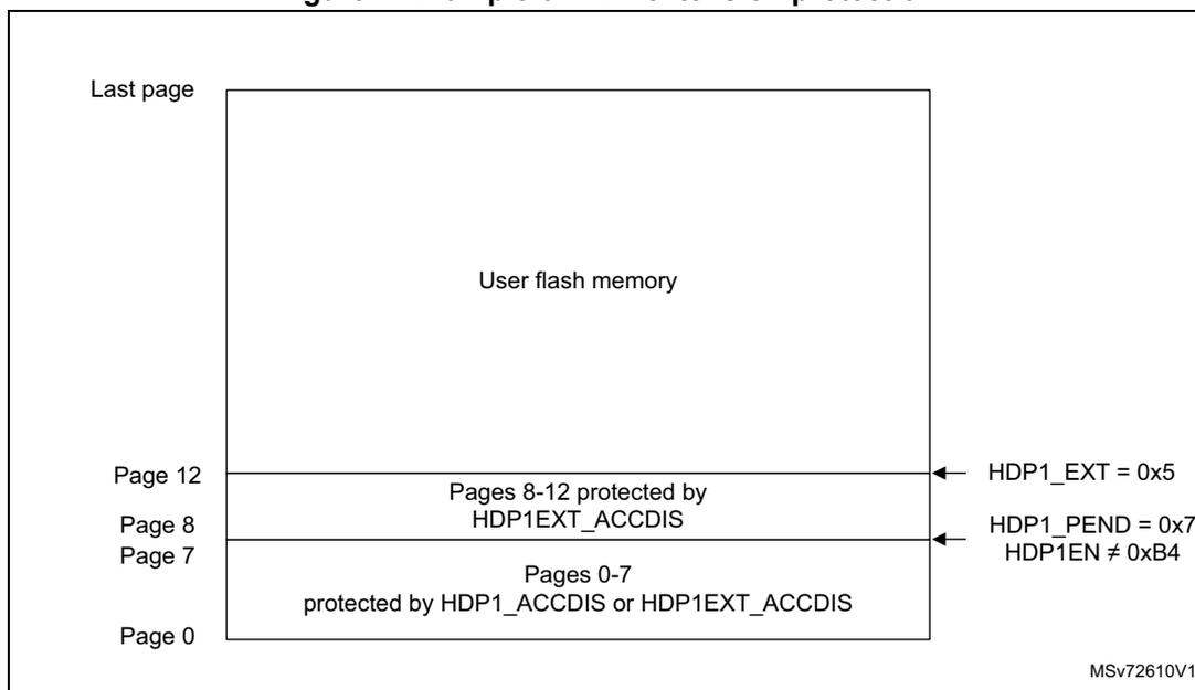
The diagram shows a vertical stack of memory pages. The top section is labeled 'Last page'. Below it is a large box labeled 'User flash memory'. At the bottom, a smaller box contains 'Pages 0-7 protected by HDP1_ACCDIS or HDP1EXT_ACCDIS'. Above this box, a line separates it from the rest of the memory, labeled 'Pages 8-12 protected by HDP1EXT_ACCDIS'. To the left of this line are labels 'Page 12', 'Page 8', and 'Page 7'. To the right of the line are labels 'HDP1_EXT = 0x5' and 'HDP1_PEND = 0x7' and 'HDP1EN ≠ 0xB4'. The bottom of the diagram is labeled 'Page 0' and 'MSV72610V1'.
As in case of HDP area configured by option bytes, any attempt to program protected pages is treated as a bus error, and fetch and read operations return zero (read-as-zero RAZ).
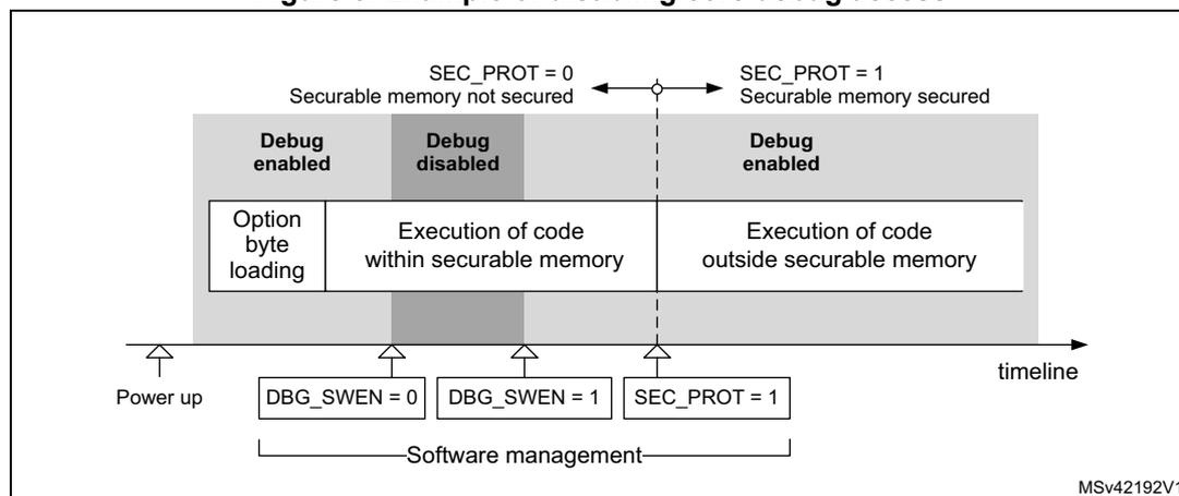
3.5.5 Disabling core debug access
For executing sensitive code or manipulating sensitive data in securable memory area, the debug access to the core can temporarily be disabled.
Figure 5 gives an example of managing DBG_SWEN and SEC_PROT bits.
Figure 5. Example of disabling core debug access
3.5.6 Forcing boot from main flash memory
To increase the security and establish a chain of trust, the BOOT_LOCK option bit of the FLASH_SECR register allows forcing the system to boot from the main flash memory regardless the other boot mode configuration bits or the empty check flag. It is always possible to set the BOOT_LOCK bit. However, it is possible to reset it only when:
- • RDP is set to level 0, or
- • RDP is set to level 1, while level 0 is requested and a full mass-erase is performed.
Caution: If BOOT_LOCK is set in association with RDP Level 1, the debug capabilities of the device are stopped, and the reset value of the DBG_SWEN bit of the FLASH_ACR register becomes zero. If the DBG_SWEN bit is cleared by the application code after reset, there is no way to recover from this situation.
3.6 FLASH interrupts
Table 18. FLASH interrupt requests
| Interrupt event | Event flag | Event flag/interrupt clearing method | Interrupt enable control bit |
|---|---|---|---|
| End of operation | EOP (1) | Write EOP=1 | EOPIE |
| Operation error | OPERR (2) | Write OPERR=1 | ERRIE |
| Write protection error | WRPERR | Write WRPERR=1 | N/A |
| Size error | SIZERR | Write SIZERR=1 | N/A |
| Programming sequential error | PROGERR | Write PROGERR=1 | N/A |
| Programming alignment error | PGAERR | Write PGAERR=1 | N/A |
Table 18. FLASH interrupt requests (continued)
| Interrupt event | Event flag | Event flag/interrupt clearing method | Interrupt enable control bit |
|---|---|---|---|
| Programming sequence error | PGSERR | Write PGSERR=1 | N/A |
| Data miss during fast programming error | MISSERR | Write MISSERR=1 | N/A |
| Fast programming error | FASTERR | Write FASTERR=1 | N/A |
- 1. EOP is set only if EOPIE is set.
- 2. OPERR is set only if ERRIE is set.
3.7 FLASH registers
3.7.1 FLASH access control register (FLASH_ACR)
Address offset: 0x000
Reset value: 0x0004 0600
| 31 | 30 | 29 | 28 | 27 | 26 | 25 | 24 | 23 | 22 | 21 | 20 | 19 | 18 | 17 | 16 |
|---|---|---|---|---|---|---|---|---|---|---|---|---|---|---|---|
| Res. | Res. | Res. | Res. | Res. | Res. | Res. | Res. | Res. | Res. | Res. | Res. | Res. | DBG_SWEN | Res. | EMPTY |
| rw | rw | ||||||||||||||
| 15 | 14 | 13 | 12 | 11 | 10 | 9 | 8 | 7 | 6 | 5 | 4 | 3 | 2 | 1 | 0 |
| Res. | Res. | Res. | Res. | ICRST | Res. | ICEN | PRFTEN | Res. | Res. | Res. | Res. | Res. | LATENCY[2:0] | ||
| w | rw | rw | rw | rw | rw | ||||||||||
Bits 31:19 Reserved, must be kept at reset value.
Bit 18 DBG_SWEN : Debug access software enable
Software may use this bit to enable/disable the debugger read access.
0: Debugger disabled
1: Debugger enabled
Bit 17 Reserved, must be kept at reset value.
Bit 16 EMPTY : Main flash memory area empty
This bit indicates whether the first location of the main flash memory area is erased or has a programmed value.
It is updated only by OBL, it is not affected by a system reset.
0: Main flash memory area programmed
1: Main flash memory area empty
The bit can be set and reset by software.
Bits 15:12 Reserved, must be kept at reset value.
Bit 11 ICRST : CPU Instruction cache reset
0: CPU Instruction cache is not reset
1: CPU Instruction cache is reset
This bit is write-only. It can be written only when the instruction cache is disabled. It is always read as zero.
Bit 10 Reserved, must be kept at reset value.
Bit 9 ICEN : CPU Instruction cache enable
0: CPU Instruction cache is disabled
1: CPU Instruction cache is enabled
Bit 8 PRFTEN : CPU Prefetch enable
0: CPU Prefetch disabled
1: CPU Prefetch enabled
Bits 7:3 Reserved, must be kept at reset value.
Bits 2:0 LATENCY[2:0] : Flash memory access latency
The value in this bitfield represents the number of CPU wait states when accessing the flash memory.
000: Zero wait states
001: One wait state
010: Two wait states
Other: Reserved
A new write into the bitfield becomes effective when it returns the same value upon read.
3.7.2 FLASH key register (FLASH_KEYR)
Address offset: 0x008
Reset value: 0x0000 0000

| 31 | 30 | 29 | 28 | 27 | 26 | 25 | 24 | 23 | 22 | 21 | 20 | 19 | 18 | 17 | 16 |
| KEY[31:16] | |||||||||||||||
| w | w | w | w | w | w | w | w | w | w | w | w | w | w | w | w |
| 15 | 14 | 13 | 12 | 11 | 10 | 9 | 8 | 7 | 6 | 5 | 4 | 3 | 2 | 1 | 0 |
| KEY[15:0] | |||||||||||||||
| w | w | w | w | w | w | w | w | w | w | w | w | w | w | w | w |
Bits 31:0 KEY[31:0] : FLASH key
The following values must be written consecutively to unlock the FLASH control register (FLASH_CR) , thus enabling programming/erasing operations:
KEY1: 0x4567 0123
KEY2: 0xCDEF 89AB
3.7.3 FLASH option key register (FLASH_OPTKEYR)
Address offset: 0x00C
Reset value: 0x0000 0000

| 31 | 30 | 29 | 28 | 27 | 26 | 25 | 24 | 23 | 22 | 21 | 20 | 19 | 18 | 17 | 16 |
| OPTKEY[31:16] | |||||||||||||||
| w | w | w | w | w | w | w | w | w | w | w | w | w | w | w | w |
| 15 | 14 | 13 | 12 | 11 | 10 | 9 | 8 | 7 | 6 | 5 | 4 | 3 | 2 | 1 | 0 |
| OPTKEY[15:0] | |||||||||||||||
| w | w | w | w | w | w | w | w | w | w | w | w | w | w | w | w |
Bits 31:0 OPTKEY[31:0] : Option byte key
The following values must be written consecutively to unlock the flash memory option registers, enabling option byte programming/erasing operations:
KEY1: 0x0819 2A3B
KEY2: 0x4C5D 6E7F
3.7.4 FLASH status register (FLASH_SR)
Address offset: 0x010
Reset value: 0x000X 0000
| 31 | 30 | 29 | 28 | 27 | 26 | 25 | 24 | 23 | 22 | 21 | 20 | 19 | 18 | 17 | 16 |
|---|---|---|---|---|---|---|---|---|---|---|---|---|---|---|---|
| Res. | Res. | Res. | Res. | Res. | Res. | Res. | Res. | Res. | Res. | OEM2 LOCK | OEM1 LOCK | Res. | CFG BSY | Res. | BSY1 |
| r | r | r | r | ||||||||||||
| 15 | 14 | 13 | 12 | 11 | 10 | 9 | 8 | 7 | 6 | 5 | 4 | 3 | 2 | 1 | 0 |
| OPTV ERR | Res. | Res. | OEMOP TWERR | HDP OPT WERR | Res. | FAST ERR | MISS ERR | PGS ERR | SIZ ERR | PGA ERR | WRP ERR | PROG ERR | Res. | OP ERR | EOP |
| rc_w1 | rc_w1 | rc_w1 | rc_w1 | rc_w1 | rc_w1 | rc_w1 | rc_w1 | rc_w1 | rc_w1 | rc_w1 | rc_w1 |
Bits 31:22 Reserved, must be kept at reset value.
Bit 21 OEM2LOCK : OEM2 lock flag
This bit indicates that the OEM2 RDP key, read during the option byte loading, is not virgin. When set, the OEM2 RDP lock mechanism is active.
Bit 20 OEM1LOCK : OEM1 lock flag
This bit indicates that the OEM1 RDP key, read during the option byte loading, is not virgin. When set, the OEM1 RDP lock mechanism is active.
Bit 19 Reserved, must be kept at reset value.
Bit 18 CFGBSY : Programming or erase configuration busy flag
The flag is set and reset by hardware.
The flag high level indicates that a program or erase operation is ongoing, based on the current FLASH control register (FLASH_CR) settings. As long as the flag remains high, the FLASH_CR register must not be written (this causes HardFault) and the software cannot start another flash memory operation.
For flash memory program operation , the flag is set when the first word is sent, and it is cleared after the second word is sent, when the operation completes or ends with an error.
For flash memory erase operation , the flag is set when setting STRT bit of FLASH control register (FLASH_CR) , and it is cleared when the operation completes or ends with an error.
Note: The flag is also set with the first byte of an access to the locked flash memory. In this case, a complete double word sent to the flash memory must be finished in order to clear the flag.
Bit 17 Reserved, must be kept at reset value.
Bit 16 BSY1 : Busy flag
This flag indicates that a flash memory operation requested by FLASH control register (FLASH_CR) is in progress. This bit is set at the beginning of the flash memory operation, and cleared when the operation finishes or when an error occurs.
Bit 15 OPTVERR : Option and engineering bits loading validity error flag
This flag is set by hardware when the options and engineering bits read may not be the one configured by the user or production. If options and engineering bits haven't been properly loaded, OPTVERR is set again after each system reset. Option bytes that fail loading are forced to a safe value, see Section 3.4.2: FLASH option byte programming .
It is cleared by programming it to 1.
Bits 14:13 Reserved, must be kept at reset value.
Bit 12 OEMOPTWERR : OEM options byte write error
This flag is set by hardware when the requested modifications of the OEM keys are not allowed.
Bit 11 HDPOPTWERR : HDP option bytes write error
This flag is set by hardware when the requested HDP related option modifications are not allowed. It is cleared by programming it to 1.
Bit 10 Reserved, must be kept at reset value.
Bit 9 FASTERR : Fast programming error flag
This flag is set by hardware when a fast programming sequence (activated by FSTPG) is interrupted due to an error (alignment, size, write protection or data miss). The corresponding status bit (PGAERR, SIZERR, WRPERR or MISSERR) is set at the same time.
It is cleared by programming it to 1.
Bit 8 MISSERR : Fast programming data miss error flag
In Fast programming mode, 32 double words (256 bytes) must be sent to flash memory successively, and the new data must be sent to the logic control before the current data is fully programmed. MISSERR is set by hardware when the new data is not present in time. It is cleared by programming it to 1.
Bit 7 PGSERR : Programming sequence error flag
This flag is set by hardware when a write access to the flash memory is performed by the code while PG or FSTPG have not been set previously. Set also by hardware when PROGERE, SIZERR, PGAERR, WRPERR, MISSERR or FASTERR is set due to a previous programming error.
It is cleared by programming it to 1.
Bit 6 SIZERR : Size error flag
This flag is set by hardware when the size of the access is a byte or half-word during a program or a fast program sequence. Only double word programming is allowed (consequently: word access).
It is cleared by programming it to 1.
Bit 5 PGAERR : Programming alignment error flag
This flag is set by hardware when the data to program cannot be contained in the same double word (64-bit) flash memory in case of standard programming, or if there is a change of page during fast programming.
It is cleared by programming it to 1.
Bit 4 WRPERR : Write protection error flag
This flag is set by hardware when an address to be erased/programmed belongs to a write-protected part (by WRP or RDP level 1) of the flash memory.
It is cleared by programming it to 1.
Bit 3 PROGERR : Programming error flag
This flag is set by hardware when a double-word address to be programmed contains a value different from 0xFFFF FFFF before programming, except if the data to write is 0x0000 0000.
It is cleared by programming it to 1.
Bit 2 Reserved, must be kept at reset value.
Bit 1 OPERR : Operation error flag
This flag is set by hardware when a flash memory operation (program / erase) completes unsuccessfully.
This bit is set only if error interrupts are enabled (ERRIE = 1).
It is cleared by programming it to 1.
Bit 0 EOP : End of operation flag
This flag is set by hardware when one or more flash memory operation (programming / erase) has been completed successfully.
This bit is set only if the end of operation interrupts are enabled (EOPIE = 1).
It is cleared by programming it to 1.
3.7.5 FLASH control register (FLASH_CR)
Address offset: 0x014
Reset value: 0xC000 0000
Access: no wait state when no flash memory operation is ongoing; word, half-word, and byte access.
Do not write this register as long as CFGBSY in FLASH status register (FLASH_SR) is high, as such a write causes a HardFault exception.
| 31 | 30 | 29 | 28 | 27 | 26 | 25 | 24 | 23 | 22 | 21 | 20 | 19 | 18 | 17 | 16 |
|---|---|---|---|---|---|---|---|---|---|---|---|---|---|---|---|
| LOCK | OPT LOCK | Res. | Res. | OBL LAUNCH | Res. | ERRIE | EOPIE | Res. | Res. | Res. | Res. | Res. | FSTPG | OPT STRT | STRT |
| rs | rs | rc_w1 | rw | rw | rw | rs | rs | ||||||||
| 15 | 14 | 13 | 12 | 11 | 10 | 9 | 8 | 7 | 6 | 5 | 4 | 3 | 2 | 1 | 0 |
| Res. | Res. | Res. | Res. | Res. | Res. | PNB[6:0] | MER1 | PER | PG | ||||||
| rw | rw | rw | rw | rw | rw | rw | rw | rw | rw | ||||||
Bit 31 LOCK : FLASH_CR Lock
This bit is set only. When set, the FLASH_CR register is locked. It is cleared by hardware after detecting the unlock sequence.
In case of an unsuccessful unlock operation, this bit remains set until the next system reset.
Bit 30 OPTLOCK : Options Lock
This bit is set only. When set, all bits concerning user option in FLASH_CR register and so option page are locked. This bit is cleared by hardware after detecting the unlock sequence. The LOCK bit must be cleared before doing the unlock sequence for OPTLOCK bit.
In case of an unsuccessful unlock operation, this bit remains set until the next reset.
Bits 29:28 Reserved, must be kept at reset value.
Bit 27 OBL_LAUNCH : Option byte load launch
When set, this bit triggers the load of option bytes into option registers. It is automatically cleared upon the completion of the load. The high state of the bit indicates pending option byte load.
The bit cannot be cleared by software. It cannot be written as long as OPTLOCK is set.
Bit 26 Reserved, must be kept at reset value.
Bit 25 ERRIE : Error interrupt enable
This bit enables the interrupt generation upon setting the OPERR flag in the FLASH_SR register.
0: Disable
1: Enable
Bit 24 EOPIE : End-of-operation interrupt enable
This bit enables the interrupt generation upon setting the EOP flag in the FLASH_SR register.
0: Disable
1: Enable
Bits 23:19 Reserved, must be kept at reset value.
Bit 18 FSTPG : Fast programming enable
0: Disable
1: Enable
Bit 17 OPTSTR : Start of modification of option bytes
This bit triggers an options operation when set.
This bit is set only by software, and is cleared when the BSY1 bit is cleared in FLASH_SR.
Bit 16 STR : Start erase operation
This bit triggers an erase operation when set.
This bit is possible to set only by software and to clear only by hardware. The hardware clears it when one of BSY1 and BSY2 flags in the FLASH_SR register transits to zero.
Bits 15:10 Reserved, must be kept at reset value.
Bits 9:3 PNB[6:0] : Page number selection
These bits select the page to erase:
0x0: page 0
0x1: page 1
...
0xF: page 15
Note: Values corresponding to addresses outside the main memory are not allowed.
Bit 2 MER1 : Mass erase
When set, this bit triggers the mass erase, that is, all user pages.
Bit 1 PER : Page erase enable
0: Disable
1: Enable
Bit 0 PG : Flash memory programming enable
0: Disable
1: Enable
3.7.6 FLASH ECC register (FLASH_ECCR)
Address offset: 0x018
Reset value: 0x0000 0000
Access: no wait state when no flash memory operation is ongoing; word, half-word, and byte access.
This register applies to single-bank products and to Bank 1 of dual-bank products.
| 31 | 30 | 29 | 28 | 27 | 26 | 25 | 24 | 23 | 22 | 21 | 20 | 19 | 18 | 17 | 16 |
|---|---|---|---|---|---|---|---|---|---|---|---|---|---|---|---|
| ECCD | ECCC | Res. | Res. | Res. | Res. | Res. | ECCIE | Res. | Res. | Res. | SYSF_ECC | Res. | Res. | Res. | Res. |
| rc_w1 | rc_w1 | rw | r | ||||||||||||
| 15 | 14 | 13 | 12 | 11 | 10 | 9 | 8 | 7 | 6 | 5 | 4 | 3 | 2 | 1 | 0 |
| Res. | Res. | ADDR_ECC[13:0] | |||||||||||||
| r | r | r | r | r | r | r | r | r | r | r | r | r | r | ||
Bit 31 ECCD: ECC detection
This flag is set by hardware when two ECC errors have been detected. When this bit is set, a NMI is generated.
It is cleared by programming it to 1.
Bit 30 ECCC: ECC correction
This flag is set by hardware when one ECC error has been detected and corrected. An interrupt is generated if ECCIE is set.
It is cleared by programming it to 1.
Bits 29:25 Reserved, must be kept at reset value.
Bit 24 ECCIE: ECC correction interrupt enable
0: ECCC interrupt disabled
1: ECCC interrupt enabled
Bits 23:21 Reserved, must be kept at reset value.
Bit 20 SYSF_ECC: System flash memory ECC fail
This bit indicates that the ECC error correction or double ECC error detection is located in the system flash memory.
Bits 19:14 Reserved, must be kept at reset value.
Bits 13:0 ADDR_ECC[13:0]: ECC fail double-word address offset
In case of ECC error or ECC correction detected, this bitfield contains double-word offset (multiple of 64 bits) to main flash memory.
3.7.7 FLASH option register (FLASH_OPTR)
Address offset: 0x020
Reset value: 0xXXXX XXXX (The option bits are loaded with values from flash memory at power-on reset release.)
Access: no wait state when no flash memory operation is ongoing; word, half-word, and byte access
| 31 | 30 | 29 | 28 | 27 | 26 | 25 | 24 | 23 | 22 | 21 | 20 | 19 | 18 | 17 | 16 |
|---|---|---|---|---|---|---|---|---|---|---|---|---|---|---|---|
| Res. | Res. | IRHEN | NRST_MODE [1:0] | N BOOT 0 | N BOOT 1 | NBOOT_SEL | BKPSRAM_HW_ERASE_DISABLE | RAM_PARITY_CHECK | BDRST | Res. | WWDG_SW | IWDG_STDBY | IWDG_STOP | IWDG_SW | |
| rw | rw | rw | rw | rw | rw | rw | rw | rw | rw | rw | rw | rw | |||
| 15 | 14 | 13 | 12 | 11 | 10 | 9 | 8 | 7 | 6 | 5 | 4 | 3 | 2 | 1 | 0 |
|---|---|---|---|---|---|---|---|---|---|---|---|---|---|---|---|
| NRST_SHDW | NRST_STDBY | NRST_STOP | Res. | Res. | BOR_LEV[1:0] | BOR_EN | RDP[7:0] | ||||||||
| rw | rw | rw | rw | rw | rw | rw | rw | rw | rw | rw | rw | rw | rw | ||
Bits 31:30 Reserved, must be kept at reset value.
Bit 29 IRHEN : Internal reset holder enable bit
0: Internal resets are propagated as simple pulse on NRST pin
1: Internal resets drives NRST pin low until it is seen as low level
Bits 28:27 NRST_MODE[1:0] : PF2-NRST pin configuration
00: Reserved
01: Reset input only: a low level on the PF2-NRST pin generates system reset; internal RESET is not propagated to the PF2-NRST pin.
10: Standard GPIO: only internal RESET is possible
11: Bidirectional reset: the PF2-NRST pin is configured in reset input/output (legacy) mode
Note: For GPIO mode, refer to Section 7.3.17: Reset pin (PF2-NRST) in GPIO mode for additional considerations.
Bit 26 NBOOT0 : NBOOT0 option bit
0: NBOOT0 = 0
1: NBOOT0 = 1
Bit 25 NBOOT1 : Boot configuration
Together with the BOOT0 pin or option bit NBOOT0 (depending on NBOOT_SEL option bit configuration), this bit selects boot mode from the main flash memory, SRAM or the system memory. Refer to Section 2.5: Boot configuration .
Bit 24 NBOOT_SEL : BOOT0 signal source selection
This option bit defines the source of the BOOT0 signal.
0: BOOT0 pin (legacy mode)
1: NBOOT0 option bit
Bit 23 BKPSRAM_HW_ERASE_DISABLE : Backup SRAM2 erase prevention
0: Backup SRAM2 is erased on system reset
1: Backup SRAM2 content is kept when a system reset occurs
The bit has no influence on other Backup SRAM2 erase requests, such as tamper or RDP regression.
- Bit 22
RAM_PARITY_CHECK
: SRAM parity check control enable/disable
0: Enable
1: Disable - Bit 21
BDRST
: Backup domain reset
0: Reset of backup domain (RTC registers and backup registers) forced on shutdown exit
1: Backup domain not reset on shutdown exit - Bit 20 Reserved, must be kept at reset value.
- Bit 19
WWDG_SW
: Window watchdog selection
0: Hardware window watchdog
1: Software window watchdog - Bit 18
IWDG_STDBY
: Independent watchdog counter freeze in Standby mode
0: Independent watchdog counter is frozen in Standby mode
1: Independent watchdog counter is running in Standby mode - Bit 17
IWDG_STOP
: Independent watchdog counter freeze in Stop mode
0: Independent watchdog counter is frozen in Stop mode
1: Independent watchdog counter is running in Stop mode - Bit 16
IWDG_SW
: Independent watchdog selection
0: Hardware independent watchdog
1: Software independent watchdog - Bit 15
NRST_SHDW
: Reset generated when entering Shutdown mode
0: Reset generated when entering the Shutdown mode
1: No reset generated when entering the Shutdown mode - Bit 14
NRST_STDBY
: Reset generated when entering Standby mode
0: Reset generated when entering the Standby mode
1: No reset generated when entering the Standby mode - Bit 13
NRST_STOP
: Reset generated when entering Stop mode
0: Reset generated when entering the Stop mode
1: No reset generated when entering the Stop mode - Bits 12:11 Reserved, must be kept at reset value.
- Bits 10:9
BOR_LEV[1:0]
: BOR reset level
This bitfield contains the V DD supply level threshold that activates/releases the reset.
00: BOR level 0, reset level threshold around 2.0 V
01: BOR level 1, reset level threshold around 2.2 V
10: BOR level 2, reset level threshold around 2.5 V
11: BOR level 3, reset level threshold around 2.8 V - Bit 8
BOR_EN
: BOR enable/disable
0: BOR disabled
1: BOR enabled - Bits 7:0
RDP[7:0]
: Read protection level
0xAA: Level 0, read protection not active
0xCC: Level 2, chip read protection active
Others: Level 1, memories read protection active
3.7.8 FLASH WRP area A address register (FLASH_WRP1AR)
Address offset: 0x02C
Reset value: 0x000X 000X (the option bits are loaded with values from flash memory at power-on reset release.)
Access: no wait state when no flash memory operation is ongoing; word, half-word, and byte access.
| 31 | 30 | 29 | 28 | 27 | 26 | 25 | 24 | 23 | 22 | 21 | 20 | 19 | 18 | 17 | 16 |
|---|---|---|---|---|---|---|---|---|---|---|---|---|---|---|---|
| Res. | Res. | Res. | Res. | Res. | Res. | Res. | Res. | Res. | WRP1A_END[6:0] | ||||||
| rw | rw | rw | rw | rw | rw | rw | |||||||||
| 15 | 14 | 13 | 12 | 11 | 10 | 9 | 8 | 7 | 6 | 5 | 4 | 3 | 2 | 1 | 0 |
| Res. | Res. | Res. | Res. | Res. | Res. | Res. | Res. | Res. | WRP1A_STR[6:0] | ||||||
| rw | rw | rw | rw | rw | rw | rw | |||||||||
Bits 31:23 Reserved, must be kept at reset value.
Bits 22:16 WRP1A_END[6:0] : WRP area A end offset
This bitfield contains the offset of the last page of the WRP area A.
Note: The number of effective bits depends on the size of the flash memory in the device.
Bits 15:7 Reserved, must be kept at reset value.
Bits 6:0 WRP1A_STR[6:0] : WRP area A start offset
This bitfield contains the offset of the first page of the WRP area A.
Note: The number of effective bits depends on the size of the flash memory in the device.
3.7.9 FLASH WRP area B address register (FLASH_WRP1BR)
Address offset: 0x030
Reset value: 0x000X 000X (the option bits are loaded with values from flash memory at power-on reset release.)
Access: no wait state when no flash memory operation is ongoing; word, half-word, and byte access.
| 31 | 30 | 29 | 28 | 27 | 26 | 25 | 24 | 23 | 22 | 21 | 20 | 19 | 18 | 17 | 16 |
|---|---|---|---|---|---|---|---|---|---|---|---|---|---|---|---|
| Res. | Res. | Res. | Res. | Res. | Res. | Res. | Res. | Res. | WRP1B_END[6:0] | ||||||
| rw | rw | rw | rw | rw | rw | rw | |||||||||
| 15 | 14 | 13 | 12 | 11 | 10 | 9 | 8 | 7 | 6 | 5 | 4 | 3 | 2 | 1 | 0 |
| Res. | Res. | Res. | Res. | Res. | Res. | Res. | Res. | Res. | WRP1B_STR[6:0] | ||||||
| rw | rw | rw | rw | rw | rw | rw | |||||||||
Bits 31:23 Reserved, must be kept at reset value.
Bits 22:16 WRP1B_END[6:0] : WRP area B end offset
This bitfield contains the offset of the last page of the WRP area B.
Note: The number of effective bits depends on the size of the flash memory in the device.
Bits 15:7 Reserved, must be kept at reset value.
Bits 6:0 WRP1B_STRT[6:0] : WRP area B start offset
This bitfield contains the offset of the first page of the WRP area B.
Note: The number of effective bits depends on the size of the flash memory in the device.
3.7.10 FLASH security register (FLASH_SECR)
Address offset: 0x080
Reset value: 0bXXXX XXXX 0000 000X 0000 0000 0XXX XXXX (the option bits are loaded with values from flash memory at power-on reset release.)
Access: no wait state when no flash memory operation is ongoing; word, half-word access.
| 31 | 30 | 29 | 28 | 27 | 26 | 25 | 24 | 23 | 22 | 21 | 20 | 19 | 18 | 17 | 16 |
|---|---|---|---|---|---|---|---|---|---|---|---|---|---|---|---|
| HDP1EN[7:0] | Res. | Res. | Res. | Res. | Res. | Res. | Res. | BOOT_LOCK | |||||||
| rw | rw | rw | rw | rw | rw | rw | rw | rw | |||||||
| 15 | 14 | 13 | 12 | 11 | 10 | 9 | 8 | 7 | 6 | 5 | 4 | 3 | 2 | 1 | 0 |
| Res. | Res. | Res. | Res. | Res. | Res. | Res. | Res. | Res. | HDP1_PEND[6:0] | ||||||
| rw | rw | rw | rw | rw | rw | rw | |||||||||
Bits 31:24 HDP1EN[7:0] : Hide protection area enable
0xB4: no HDP area
Others: HDP area enabled
Bits 23:17 Reserved, must be kept at reset value.
Bit 16 BOOT_LOCK : Forced boot from user area
0: Boot based on the pad/option bit configuration
1: Boot forced from main flash memory
Caution: If BOOT_LOCK is set in association with RDP Level 1, the debug capabilities of the device are stopped, and the reset value of the DBG_SWEN bit of the FLASH_ACR register becomes zero. If the DBG_SWEN bit is cleared by the application code after reset, there is no way to recover from this situation.
Bits 15:7 Reserved, must be kept at reset value.
Bits 6:0 HDP1_PEND[6:0] : Last page of the first hide protection area
This bitfield contains the last page of the HDP area.
3.7.11 FLASH OEM1 key register 1 (FLASH_OEM1KEYR1)
Address offset: 0x088
Reset value: 0xFFFF FFFF
Access: no wait state when no flash memory operation is ongoing; word, half-word access.
| 31 | 30 | 29 | 28 | 27 | 26 | 25 | 24 | 23 | 22 | 21 | 20 | 19 | 18 | 17 | 16 |
|---|---|---|---|---|---|---|---|---|---|---|---|---|---|---|---|
| OEM1KEY[31:16] | |||||||||||||||
| w | w | w | w | w | w | w | w | w | w | w | w | w | w | w | w |
| 15 | 14 | 13 | 12 | 11 | 10 | 9 | 8 | 7 | 6 | 5 | 4 | 3 | 2 | 1 | 0 |
| OEM1KEY[15:0] | |||||||||||||||
| w | w | w | w | w | w | w | w | w | w | w | w | w | w | w | w |
Bits 31:0
OEM1KEY[31:0]
: Bits 31 to 0 of the OEM1 key
All bits are write-only and always read as zero.
3.7.12 FLASH OEM1 key register 2 (FLASH_OEM1KEYR2)
Address offset: 0x08C
Reset value: 0xFFFF FFFF
Access: no wait state when no option bytes modification is ongoing; word, half-word, and byte access
| 31 | 30 | 29 | 28 | 27 | 26 | 25 | 24 | 23 | 22 | 21 | 20 | 19 | 18 | 17 | 16 |
|---|---|---|---|---|---|---|---|---|---|---|---|---|---|---|---|
| OEM1KEY[63:48] | |||||||||||||||
| w | w | w | w | w | w | w | w | w | w | w | w | w | w | w | w |
| 15 | 14 | 13 | 12 | 11 | 10 | 9 | 8 | 7 | 6 | 5 | 4 | 3 | 2 | 1 | 0 |
| OEM1KEY[47:32] | |||||||||||||||
| w | w | w | w | w | w | w | w | w | w | w | w | w | w | w | w |
Bits 31:0
OEM1KEY[63:32]
: Bits 63 to 32 of the OEM1 key
All bits are write-only and always read as zero.
3.7.13 FLASH OEM1 key register 3 (FLASH_OEM1KEYR3)
Address offset: 0x090
Reset value: 0xFFFF FFFF
Access: no wait state when no option bytes modification is ongoing; word, half-word, and byte access
| 31 | 30 | 29 | 28 | 27 | 26 | 25 | 24 | 23 | 22 | 21 | 20 | 19 | 18 | 17 | 16 |
|---|---|---|---|---|---|---|---|---|---|---|---|---|---|---|---|
| OEM1KEY[95:80] | |||||||||||||||
| w | w | w | w | w | w | w | w | w | w | w | w | w | w | w | w |
| 15 | 14 | 13 | 12 | 11 | 10 | 9 | 8 | 7 | 6 | 5 | 4 | 3 | 2 | 1 | 0 |
| OEM1KEY[79:64] | |||||||||||||||
| w | w | w | w | w | w | w | w | w | w | w | w | w | w | w | w |
Bits 31:0
OEM1KEY[95:64]
: Bits 95 to 64 of the OEM1 key
All bits are write-only and always read as zero.
3.7.14 FLASH OEM1 key register 4 (FLASH_OEM1KEYR4)
Address offset: 0x094
Reset value: 0xFFFF FFFF
Access: no wait state when no option bytes modification is ongoing; word, half-word, and byte access
| 31 | 30 | 29 | 28 | 27 | 26 | 25 | 24 | 23 | 22 | 21 | 20 | 19 | 18 | 17 | 16 |
| OEM1KEY[127:112] | |||||||||||||||
| w | w | w | w | w | w | w | w | w | w | w | w | w | w | w | w |
| 15 | 14 | 13 | 12 | 11 | 10 | 9 | 8 | 7 | 6 | 5 | 4 | 3 | 2 | 1 | 0 |
| OEM1KEY[111:96] | |||||||||||||||
| w | w | w | w | w | w | w | w | w | w | w | w | w | w | w | w |
Bits 31:0
OEM1KEY[127:96]
: Bits 127 to 96 of the OEM1 key
All bits are write-only and always read as zero.
3.7.15 FLASH OEM2 key register 1 (FLASH_OEM2KEYR1)
Address offset: 0x098
Reset value: 0xFFFF FFFF
Access: no wait state when no flash memory operation is ongoing; word, half-word access.
| 31 | 30 | 29 | 28 | 27 | 26 | 25 | 24 | 23 | 22 | 21 | 20 | 19 | 18 | 17 | 16 |
| OEM2KEY[31:16] | |||||||||||||||
| w | w | w | w | w | w | w | w | w | w | w | w | w | w | w | w |
| 15 | 14 | 13 | 12 | 11 | 10 | 9 | 8 | 7 | 6 | 5 | 4 | 3 | 2 | 1 | 0 |
| OEM2KEY[15:0] | |||||||||||||||
| w | w | w | w | w | w | w | w | w | w | w | w | w | w | w | w |
Bits 31:0
OEM2KEY[31:0]
: Bits 31 to 0 of the OEM2 key
All bits are write-only and always read as zero.
3.7.16 FLASH OEM2 key register 2 (FLASH_OEM2KEYR2)
Address offset: 0x09C
Reset value: 0xFFFF FFFF
Access: no wait state when no option bytes modification is ongoing; word, half-word, and byte access

| 31 | 30 | 29 | 28 | 27 | 26 | 25 | 24 | 23 | 22 | 21 | 20 | 19 | 18 | 17 | 16 |
| OEM2KEY[63:48] | |||||||||||||||
| w | w | w | w | w | w | w | w | w | w | w | w | w | w | w | w |
| 15 | 14 | 13 | 12 | 11 | 10 | 9 | 8 | 7 | 6 | 5 | 4 | 3 | 2 | 1 | 0 |
| OEM2KEY[47:32] | |||||||||||||||
| w | w | w | w | w | w | w | w | w | w | w | w | w | w | w | w |
Bits 31:0
OEM2KEY[63:32]
: Bits 63 to 32 of the OEM2 key
All bits are write-only and always read as zero.
3.7.17 FLASH OEM2 key register 3 (FLASH_OEM2KEYR3)
Address offset: 0x0A0
Reset value: 0xFFFF FFFF
Access: no wait state when no option bytes modification is ongoing; word, half-word, and byte access

| 31 | 30 | 29 | 28 | 27 | 26 | 25 | 24 | 23 | 22 | 21 | 20 | 19 | 18 | 17 | 16 |
| OEM2KEY[95:80] | |||||||||||||||
| w | w | w | w | w | w | w | w | w | w | w | w | w | w | w | w |
| 15 | 14 | 13 | 12 | 11 | 10 | 9 | 8 | 7 | 6 | 5 | 4 | 3 | 2 | 1 | 0 |
| OEM2KEY[79:64] | |||||||||||||||
| w | w | w | w | w | w | w | w | w | w | w | w | w | w | w | w |
Bits 31:0
OEM2KEY[95:64]
: Bits 95 to 64 of the OEM2 key
All bits are write-only and always read as zero.
3.7.18 FLASH OEM2 key register 4 (FLASH_OEM2KEYR4)
Address offset: 0x0A4
Reset value: 0xFFFF FFFF
Access: no wait state when no option bytes modification is ongoing; word, half-word, and byte access

| 31 | 30 | 29 | 28 | 27 | 26 | 25 | 24 | 23 | 22 | 21 | 20 | 19 | 18 | 17 | 16 |
| OEM2KEY[127:112] | |||||||||||||||
| w | w | w | w | w | w | w | w | w | w | w | w | w | w | w | w |
| 15 | 14 | 13 | 12 | 11 | 10 | 9 | 8 | 7 | 6 | 5 | 4 | 3 | 2 | 1 | 0 |
| OEM2KEY[111:96] | |||||||||||||||
| w | w | w | w | w | w | w | w | w | w | w | w | w | w | w | w |
Bits 31:0
OEM2KEY[127:96]
: Bits 127 to 96 of the OEM2 key
All bits are write-only and always read as zero.
3.7.19 FLASH OEM key status register (FLASH_OEMKEYSR)
Address offset: 0x0A8
Reset value: 0x00XX 00XX (where XX represent the CRC value calculated from the current OEM keys)
Access: no wait state when no flash memory operation is ongoing; word, half-word access.
| 31 | 30 | 29 | 28 | 27 | 26 | 25 | 24 | 23 | 22 | 21 | 20 | 19 | 18 | 17 | 16 |
|---|---|---|---|---|---|---|---|---|---|---|---|---|---|---|---|
| Res. | Res. | Res. | Res. | Res. | Res. | Res. | Res. | OEM2KEYCRC[7:0] | |||||||
| r | r | r | r | r | r | r | r | ||||||||
| 15 | 14 | 13 | 12 | 11 | 10 | 9 | 8 | 7 | 6 | 5 | 4 | 3 | 2 | 1 | 0 |
| Res. | Res. | Res. | Res. | Res. | Res. | Res. | Res. | OEM1KEYCRC[7:0] | |||||||
| r | r | r | r | r | r | r | r | ||||||||
Bits 31:24 Reserved, must be kept at reset value.
Bits 23:16 OEM2KEYCRC[7:0] : 8-bit CRC value calculated from the OEM2 key
This bitfield contains the read-only 8-bit CRC value calculated from the OEM2 128-bit key.
This value is calculated using the following CRC parameters:
Polynomial = 0x7
Initial value = 0x0 (128 bits)
Final XoR = 0x5
Bits 15:8 Reserved, must be kept at reset value.
Bits 7:0 OEM1KEYCRC[7:0] : 8-bit CRC value calculated from the OEM1 key
This bitfield contains the read-only 8-bit CRC value calculated from the OEM1 128-bit key.
This value is calculated using the following CRC parameters:
Polynomial = 0x7
Initial value = 0x0 (128 bits)
Final XoR = 0x5
3.7.20 FLASH HDP control register (FLASH_HDPCR)
Address offset: 0x0AC
Reset value: 0x00A3 00A3
Access: no wait state when no flash memory operation is ongoing; word, half-word access.
| 31 | 30 | 29 | 28 | 27 | 26 | 25 | 24 | 23 | 22 | 21 | 20 | 19 | 18 | 17 | 16 |
|---|---|---|---|---|---|---|---|---|---|---|---|---|---|---|---|
| Res. | Res. | Res. | Res. | Res. | Res. | Res. | Res. | HDP1EXT_ACCDIS[7:0] | |||||||
| rw | rw | rw | rw | rw | rw | rw | rw | ||||||||
| 15 | 14 | 13 | 12 | 11 | 10 | 9 | 8 | 7 | 6 | 5 | 4 | 3 | 2 | 1 | 0 |
| Res. | Res. | Res. | Res. | Res. | Res. | Res. | Res. | HDP1_ACCDIS[7:0] | |||||||
| rw | rw | rw | rw | rw | rw | rw | rw | ||||||||
Bits 31:24 Reserved, must be kept at reset value.
Bits 23:16 HDP1EXT_ACCDIS[7:0] : HDP1 extension area access disable
The access to this register depends on its current value. Refer to Section 3.5.4: Securable memory area extension (HDP extension) for the full conditions.
0xA3: Access to HDP1 extension area is granted
0x5C: Access to HDP1 extension area is denied, but incrementing HDP1_EXT[6:0] of FLASH_HDPEXTR register is allowed at any time (modifying HDP1EN[7:0]/HDP1_PEND[7:0] option bytes is not allowed)
Others: Access to HDP1 extension area is denied, and updating the size of HDP1 extension area is not possible since writing to HDP1_EXT[6:0] is denied (modifying HDP1EN[7:0]/HDP1_PEND[7:0] option bytes is not allowed).
Bits 15:8 Reserved, must be kept at reset value.
Bits 7:0 HDP1_ACCDIS[7:0] : HDP1 area access disable
When set to a value different from 0xA3, this bitfield cannot be modified except by a system reset. In this case, any write access to HDP1_ACCDIS[7:0] is ignored.
0xA3: Access to HDP1 area granted
Others: Access to HDP1 area denied (modifying HDP1EN[7:0]/HDP1_PEND[7:0] option bytes is not allowed).
3.7.21 FLASH HDP extension register (FLASH_HDPEXTR)
Address offset: 0x0B0
Reset value: 0x0000 0000
Access: no wait state when no flash memory operation is ongoing; word, half-word access.
| 31 | 30 | 29 | 28 | 27 | 26 | 25 | 24 | 23 | 22 | 21 | 20 | 19 | 18 | 17 | 16 |
|---|---|---|---|---|---|---|---|---|---|---|---|---|---|---|---|
| Res. | Res. | Res. | Res. | Res. | Res. | Res. | Res. | Res. | Res. | Res. | Res. | Res. | Res. | Res. | Res. |
| 15 | 14 | 13 | 12 | 11 | 10 | 9 | 8 | 7 | 6 | 5 | 4 | 3 | 2 | 1 | 0 |
| Res. | Res. | Res. | Res. | Res. | Res. | Res. | Res. | Res. | HDP1_EXT[6:0] | ||||||
| rw | rw | rw | rw | rw | rw | rw | |||||||||
Bits 31:7 Reserved, must be kept at reset value.
Bits 6:0 HDP1_EXT[6:0] : HDP1 extension area size
Size of the HDP1 extension area expressed in number of 2-Kbyte pages. The extension starts at page offset HDP1_PEND[7:0] + 1.
Register access depends on the value of HDP1EXT_ACCDIS[7:0] in the FLASH_HDPCR register.
3.7.22 FLASH register map
Table 19. FLASH register map and reset values
| Offset | Register | 31 | 30 | 29 | 28 | 27 | 26 | 25 | 24 | 23 | 22 | 21 | 20 | 19 | 18 | 17 | 16 | 15 | 14 | 13 | 12 | 11 | 10 | 9 | 8 | 7 | 6 | 5 | 4 | 3 | 2 | 1 | 0 | |
|---|---|---|---|---|---|---|---|---|---|---|---|---|---|---|---|---|---|---|---|---|---|---|---|---|---|---|---|---|---|---|---|---|---|---|
| 0x000 | FLASH_ACR | Res. | Res. | Res. | Res. | Res. | Res. | Res. | Res. | Res. | Res. | Res. | Res. | Res. | DBG_SWEN | Res. | EMPTY | Res. | Res. | Res. | Res. | ICRST | Res. | ICEN | PRFTEN | Res. | Res. | Res. | Res. | Res. | LATENCY [2:0] | |||
| Reset value | 1 | X | 0 | 1 | 0 | 0 | 0 | 0 | ||||||||||||||||||||||||||
| 0x004 | Reserved | Res. | Res. | Res. | Res. | Res. | Res. | Res. | Res. | Res. | Res. | Res. | Res. | Res. | Res. | Res. | Res. | Res. | Res. | Res. | Res. | Res. | Res. | Res. | Res. | Res. | Res. | Res. | Res. | Res. | Res. | Res. | Res. | |
| 0x008 | FLASH_KEYR | KEYR[31:0] | ||||||||||||||||||||||||||||||||
| Reset value | 0 | 0 | 0 | 0 | 0 | 0 | 0 | 0 | 0 | 0 | 0 | 0 | 0 | 0 | 0 | 0 | 0 | 0 | 0 | 0 | 0 | 0 | 0 | 0 | 0 | 0 | 0 | 0 | 0 | 0 | 0 | 0 | ||
| 0x00C | FLASH_OPT_KEYR | OPTKEY[31:0] | ||||||||||||||||||||||||||||||||
| Reset value | 0 | 0 | 0 | 0 | 0 | 0 | 0 | 0 | 0 | 0 | 0 | 0 | 0 | 0 | 0 | 0 | 0 | 0 | 0 | 0 | 0 | 0 | 0 | 0 | 0 | 0 | 0 | 0 | 0 | 0 | 0 | 0 | ||
| 0x010 | FLASH_SR | Res. | Res. | Res. | Res. | Res. | Res. | Res. | Res. | Res. | OEM2LOCK | OEM1LOCK | Res. | CFGBSY | Res. | BSY1 | OPTVERR | Res. | Res. | Res. | OEMOPTWERR | HDOPTWERR | Res. | FASTERR | MISERR | PGSERR | SIZERR | PGAERR | WRPERR | PROGERR | Res. | OPERR | EOP | |
| Reset value | 0 | 0 | 0 | 0 | X | 0 | 0 | 0 | 0 | 0 | 0 | 0 | 0 | 0 | 0 | 0 | ||||||||||||||||||
| 0x014 | FLASH_CR | LOCK | OPTLOCK | Res. | Res. | OBL_LAUNCH | Res. | ERRIE | EOPIE | Res. | Res. | Res. | Res. | FSTPG | OPTSTRT | STRT | Res. | Res. | Res. | Res. | Res. | Res. | Res. | PNB[6:0] | MER1 | PER | PG | |||||||
| Reset value | 1 | 1 | 0 | 0 | 0 | 0 | 0 | 0 | 0 | 0 | 0 | 0 | 0 | 0 | 0 | 0 | 0 | 0 | ||||||||||||||||
| 0x018 | FLASH_ECCR | ECCD | ECCC | Res. | Res. | Res. | Res. | Res. | ECCIE | Res. | Res. | Res. | SYSF_ECC | Res. | Res. | Res. | Res. | Res. | Res. | ADDR_ECC[13:0] | ||||||||||||||
| Reset value | 0 | 0 | 0 | 0 | 0 | 0 | 0 | 0 | 0 | 0 | 0 | 0 | 0 | 0 | 0 | 0 | 0 | 0 | ||||||||||||||||
| 0x020 | FLASH_OPTR | Res. | Res. | IRHEN | NRST_MODE[1:0] | NBOOT0 | NBOOT1 | NBOOT_SEL | BKPSRAM_HW_ERASE_DISABLE | RAM_PARITY_CHECK | BDRST | Res. | WWDG_SW | IWDG_STBY | IWDG_STOP | IWDG_SW | NRST_SHDW | NRST_STDBY | NRST_STOP | Res. | Res. | Res. | BOR_LEV[1:0] | BOR_EN | RDP[7:0] | |||||||||
| Reset value | X | X | X | X | X | X | X | X | X | X | X | X | X | X | X | X | X | X | X | X | X | X | X | X | X | X | ||||||||
| 0x024 - 0x028 | Reserved | Res. | Res. | Res. | Res. | Res. | Res. | Res. | Res. | Res. | Res. | Res. | Res. | Res. | Res. | Res. | Res. | Res. | Res. | Res. | Res. | Res. | Res. | Res. | Res. | Res. | Res. | Res. | Res. | Res. | Res. | Res. | Res. | |
| 0x02C | FLASH_WRP1AR | Res. | Res. | Res. | Res. | Res. | Res. | Res. | Res. | Res. | Res. | Res. | Res. | WRP1A_END [3:0] | Res. | Res. | Res. | Res. | Res. | Res. | Res. | Res. | Res. | WRP1A_STRT[6:0] | ||||||||||
| Reset value | X | X | X | X | X | X | X | X | X | X | X | |||||||||||||||||||||||
| 0x030 | FLASH_WRP1BR | Res. | Res. | Res. | Res. | Res. | Res. | Res. | Res. | Res. | Res. | Res. | Res. | WRP1B_END [3:0] | Res. | Res. | Res. | Res. | Res. | Res. | Res. | Res. | Res. | WRP1B_STRT[6:0] | ||||||||||
| Reset value | X | X | X | X | X | X | X | X | X | X | X | |||||||||||||||||||||||
| 0x034 - 0x07F | Reserved | Res. | Res. | Res. | Res. | Res. | Res. | Res. | Res. | Res. | Res. | Res. | Res. | Res. | Res. | Res. | Res. | Res. | Res. | Res. | Res. | Res. | Res. | Res. | Res. | Res. | Res. | Res. | Res. | Res. | Res. | Res. | Res. | |
Table 19. FLASH register map and reset values (continued)
| Offset | Register | 31 | 30 | 29 | 28 | 27 | 26 | 25 | 24 | 23 | 22 | 21 | 20 | 19 | 18 | 17 | 16 | 15 | 14 | 13 | 12 | 11 | 10 | 9 | 8 | 7 | 6 | 5 | 4 | 3 | 2 | 1 | 0 |
|---|---|---|---|---|---|---|---|---|---|---|---|---|---|---|---|---|---|---|---|---|---|---|---|---|---|---|---|---|---|---|---|---|---|
| 0x080 | FLASH_SECR | HDP1EN[7:0] | Res | Res | Res | Res | Res | Res | Res | Res | BOOT_LOCK | Res | Res | Res | Res | Res | Res | Res | Res | Res | Res | HDP1_PEND[6:0] | |||||||||||
| Reset value | X | X | X | X | X | X | X | X | X | X | X | X | X | X | X | X | |||||||||||||||||
| 0x084 | Reserved | Res | Res | Res | Res | Res | Res | Res | Res | Res | Res | Res | Res | Res | Res | Res | Res | Res | Res | Res | Res | Res | Res | Res | Res | Res | Res | Res | Res | Res | Res | Res | Res |
| 0x088 | FLASH_OEM1KEYR1 | OEM1KEY[31:0] | |||||||||||||||||||||||||||||||
| Reset value | X | X | X | X | X | X | X | X | X | X | X | X | X | X | X | X | X | X | X | X | X | X | X | X | X | X | X | X | X | X | X | X | |
| 0x08C | FLASH_OEM1KEYR2 | OEM1KEY[63:32] | |||||||||||||||||||||||||||||||
| Reset value | X | X | X | X | X | X | X | X | X | X | X | X | X | X | X | X | X | X | X | X | X | X | X | X | X | X | X | X | X | X | X | X | |
| 0x090 | FLASH_OEM1KEYR3 | OEM1KEY[95:64] | |||||||||||||||||||||||||||||||
| Reset value | X | X | X | X | X | X | X | X | X | X | X | X | X | X | X | X | X | X | X | X | X | X | X | X | X | X | X | X | X | X | X | X | |
| 0x094 | FLASH_OEM1KEYR4 | OEM1KEY[127:96] | |||||||||||||||||||||||||||||||
| Reset value | X | X | X | X | X | X | X | X | X | X | X | X | X | X | X | X | X | X | X | X | X | X | X | X | X | X | X | X | X | X | X | X | |
| 0x098 | FLASH_OEM2KEYR1 | OEM2KEY[31:0] | |||||||||||||||||||||||||||||||
| Reset value | X | X | X | X | X | X | X | X | X | X | X | X | X | X | X | X | X | X | X | X | X | X | X | X | X | X | X | X | X | X | X | X | |
| 0x09C | FLASH_OEM2KEYR2 | OEM2KEY[63:32] | |||||||||||||||||||||||||||||||
| Reset value | X | X | X | X | X | X | X | X | X | X | X | X | X | X | X | X | X | X | X | X | X | X | X | X | X | X | X | X | X | X | X | X | |
| 0x0A0 | FLASH_OEM2KEYR3 | OEM2KEY[95:64] | |||||||||||||||||||||||||||||||
| Reset value | X | X | X | X | X | X | X | X | X | X | X | X | X | X | X | X | X | X | X | X | X | X | X | X | X | X | X | X | X | X | X | X | |
| 0x0A4 | FLASH_OEM2KEYR4 | OEM2KEY[127:96] | |||||||||||||||||||||||||||||||
| Reset value | X | X | X | X | X | X | X | X | X | X | X | X | X | X | X | X | X | X | X | X | X | X | X | X | X | X | X | X | X | X | X | X | |
| 0x0A8 | FLASH_KEYSR | Res | Res | Res | Res | Res | Res | Res | Res | OEM2KEYCRC[7:0] | Res | Res | Res | Res | Res | Res | Res | Res | Res | Res | Res | OEM1KEYCRC[7:0] | |||||||||||
| Reset value | X | X | X | X | X | X | X | X | X | X | X | X | X | X | X | ||||||||||||||||||
| 0x0AC | FLASH_HDPCR | Res | Res | Res | Res | Res | Res | Res | Res | HDP1EXT_ACCDIS[7:0] | Res | Res | Res | Res | Res | Res | Res | Res | Res | Res | Res | HDP1_ACCDIS[7:0] | |||||||||||
| Reset value | 1 | 0 | 1 | 0 | 0 | 0 | 1 | 1 | 1 | 0 | 1 | 0 | 0 | 0 | 1 | 1 | |||||||||||||||||
| 0x0B0 | FLASH_HDPEXTR | Res | Res | Res | Res | Res | Res | Res | Res | Res | Res | Res | Res | Res | Res | Res | Res | Res | Res | Res | Res | Res | Res | Res | Res | Res | Res | HDP1_EXT[6:0] | |||||
| Reset value | 0 | 0 | 0 | 0 | 0 | 0 | |||||||||||||||||||||||||||