2. Memory and bus architecture
2.1 System architecture
The main system consists of:
- • Two masters:
- – Cortex ® -M0+ core
- – General-purpose DMA
- • Three slaves:
- – Internal SRAM
- – Internal flash memory
- – AHB with AHB-to-APB bridge that connects all the APB peripherals
These are interconnected using a multilayer AHB bus architecture as shown in Figure 1 .
Figure 1. System architecture
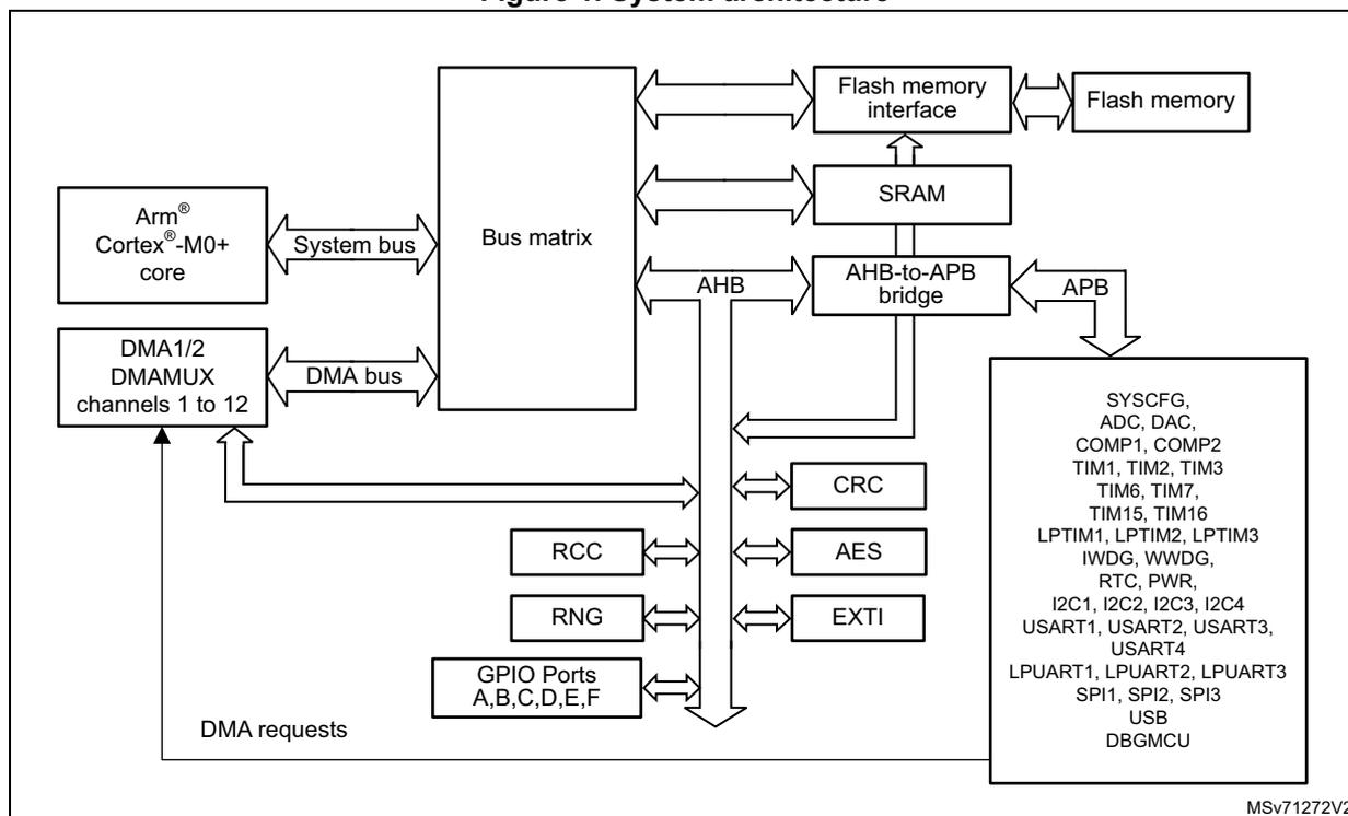
The diagram illustrates the system architecture. At the center is a 'Bus matrix'. To its left, the 'Arm ® Cortex ® -M0+ core' is connected via a 'System bus', and 'DMA1/2 DMAMUX channels 1 to 12' are connected via a 'DMA bus'. Below the DMA, 'DMA requests' are shown. The Bus matrix is connected to several components: 'Flash memory interface' (which connects to 'Flash memory'), 'SRAM', and 'AHB-to-APB bridge'. The AHB-to-APB bridge connects to an 'APB' bus, which in turn connects to a large block of peripherals including SYSCFG, ADC, DAC, COMP1, COMP2, TIM1, TIM2, TIM3, TIM6, TIM7, TIM15, TIM16, LPTIM1, LPTIM2, LPTIM3, IWDG, WWDG, RTC, PWR, I2C1, I2C2, I2C3, I2C4, USART1, USART2, USART3, USART4, LPUART1, LPUART2, LPUART3, SPI1, SPI2, SPI3, USB, and DBGMCU. The Bus matrix also connects to 'RCC', 'RNG', 'GPIO Ports A,B,C,D,E,F', 'CRC', 'AES', and 'EXTI'. The diagram is labeled 'MSv71272V2' in the bottom right corner.
System bus (S-bus)
This bus connects the system bus of the Cortex ® -M0+ core (peripheral bus) to a bus matrix that manages the arbitration between the core and the DMA.
DMA bus
This bus connects the AHB master interface of the DMA to the bus matrix that manages the access of CPU and DMA to SRAM, flash memory and AHB/APB peripherals.
Bus matrix
The bus matrix manages the access arbitration between the core system bus and the DMA master bus. The arbitration uses a Round Robin algorithm. The bus matrix is composed of masters (CPU, DMA) and slaves (flash memory interface, SRAM and AHB-to-APB bridge).
AHB peripherals are connected on system bus through the bus matrix to allow DMA access.
AHB-to-APB bridge (APB)
The AHB-to-APB bridge provides full synchronous connections between the AHB and the APB bus.
Refer to Section 2.2: Memory organization for the address mapping of the peripherals connected to this bridge.
After each device reset, all peripheral clocks are disabled (except for the SRAM and flash memory). Before using a peripheral its clock in the RCC_AHBENR, RCC_APBENRx or RCC_IOPENR register must first be enabled.
Note: When a 16- or 8-bit access is performed on an APB register, the access is transformed into a 32-bit access: the bridge duplicates the 16- or 8-bit data to feed the 32-bit vector.
2.2 Memory organization
2.2.1 Introduction
Program memory, data memory, registers and I/O ports are organized within the same linear 4-Gbyte address space.
The bytes are coded in memory in Little Endian format. The lowest numbered byte in a word is considered the word's least significant byte and the highest numbered byte the most significant.
2.2.2 Memory map and register boundary addresses
Figure 2. Memory map
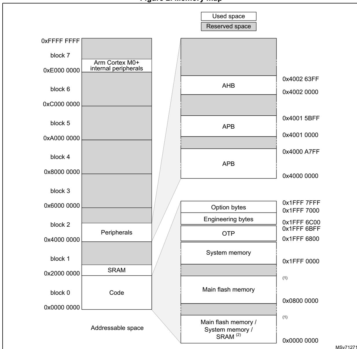
Legend:
- Used space
- Reserved space
Memory Map Details:
- Addressable space: 0x0000 0000 to 0xFFFF FFFF
- Block 7: 0xE000 0000 to 0xFFFF FFFF (Arm Cortex M0+ internal peripherals)
- Block 6: 0xC000 0000 to 0xE000 0000 (Reserved)
- Block 5: 0xA000 0000 to 0xC000 0000 (Reserved)
- Block 4: 0x8000 0000 to 0xA000 0000 (Reserved)
- Block 3: 0x6000 0000 to 0x8000 0000 (Reserved)
- Block 2: 0x4000 0000 to 0x6000 0000 (Peripherals)
- Block 1: 0x2000 0000 to 0x4000 0000 (SRAM)
- Block 0: 0x0000 0000 to 0x2000 0000 (Code)
Zoomed-in View (Lower Address Range):
- 0x0000 0000 to 0x0800 0000: Main flash memory / System memory / SRAM (2)
- 0x0800 0000 to 0x1FFF 0000: Main flash memory
- 0x1FFF 0000 to 0x1FFF 6800: System memory
- 0x1FFF 6800 to 0x1FFF 6BFF: OTP
- 0x1FFF 6BFF to 0x1FFF 7000: Engineering bytes
- 0x1FFF 7000 to 0x1FFF 7FFF: Option bytes
- 0x4000 0000 to 0x4000 A7FF: APB
- 0x4001 0000 to 0x4001 5BFF: APB
- 0x4002 0000 to 0x4002 63FF: AHB
Notes:
- STM32U073xx and STM32U083xx: 0x0803 FFFF; STM32U031xx: 0x0800 FFFF.
- Depends on boot configuration.
MSV71271
1. STM32U073xx and STM32U083xx: 0x0803 FFFF; STM32U031xx: 0x0800 FFFF.
2. Depends on boot configuration.
All the memory map areas that are not allocated to on-chip memories and peripherals are considered as reserved. For the detailed mapping of available memory and register areas, refer to the following tables.
Table 2. STM32U073xx and STM32U083xx memory boundary addresses| Type | Boundary address | Size | Memory Area | Register description |
|---|---|---|---|---|
| SRAM | 0x2002 A000 - 0x3FFF FFFF | ~512 Mbytes | Reserved | - |
| 0x2000 0000 - 0x2002 9FFF | 40 Kbytes | SRAM | Section 2.3 on page 60 | |
| Code | 0x1FFF 8000 - 0x1FFF FFFF | ~34 Kbytes | Reserved | - |
| 0x1FFF 7000 - 0x1FFF 7FFF | 4 Kbytes | Option bytes | Section 3.4 on page 75 | |
| 0x1FFF 6C00 - 0x1FFF 6FFF | 1 Kbyte | Engineering bytes | - | |
| 0x1FFF 6800 - 0x1FFF 6BFF | 1 Kbyte | OTP | - | |
| 0x1FFF 0000 - 0x1FFF 67FF | 26 Kbytes | System memory | - | |
| 0x0808 0000 - 0x1FFF D7FF | ~384 Mbytes | Reserved | - | |
| 0x0800 0000 - 0x0803 FFFF | 256 Kbytes | Main flash memory | Section 3.3.1 on page 65 | |
| 0x0008 0000 - 0x07FF FFFF | ~7.75 Mbytes | Reserved | - | |
| 0x0000 0000 - 0x0003 FFFF (1) | 256 Kbytes | Main flash memory, system memory or SRAM depending on BOOT configuration | - |
1. The memory boundary depends on the memory size of the ordered devices.
Table 3. STM32U031xx memory boundary addresses| Type | Boundary address | Size | Memory Area | Register description |
|---|---|---|---|---|
| SRAM | 0x2000 A000 - 0x3FFF FFFF | ~512 Mbytes | Reserved | - |
| 0x2000 0000 - 0x2000 2FFF | 12 Kbytes | SRAM | Section 2.3 on page 60 | |
| Code | 0x1FFF 8000 - 0x1FFF FFFF | ~34 Kbytes | Reserved | - |
| 0x1FFF 7000 - 0x1FFF 7FFF | 4 Kbytes | Option bytes | Section 3.4 on page 75 | |
| 0x1FFF 6C00 - 0x1FFF 6FFF | 1 Kbyte | Engineering bytes | - | |
| 0x1FFF 6800 - 0x1FFF 6BFF | 1 Kbyte | OTP | - | |
| 0x1FFF 0000 - 0x1FFF 67FF | 26 Kbytes | System memory | - | |
| 0x0802 0000 - 0x1FFF D7FF | ~384 Mbytes | Reserved | - | |
| 0x0800 0000 - 0x0801 FFFF | 64 Kbytes | Main flash memory | Section 3.3.1 on page 65 | |
| 0x0002 0000 - 0x07FF FFFF | ~8 Mbytes | Reserved | - | |
| 0x0000 0000 - 0x0001 FFFF (1) | 64 Kbytes | Main flash memory, system memory or SRAM depending on BOOT configuration | - |
1. The memory boundary depends on the memory size of the ordered devices.
The following table gives the boundary addresses of the peripherals.
Table 4. STM32U0 series peripheral register boundary addresses
| Bus | Boundary address | Size | Peripheral | Peripheral register map |
|---|---|---|---|---|
| - | 0xE000 0000 - 0xE00F FFFF | 1Mbytes | Cortex®-M0+ internal peripherals | - |
| AHB | 0x5000 1800 - 0x5FFF FFFF | ~256 Mbytes | Reserved | - |
| 0x5000 1400 - 0x5000 17FF | 1 Kbyte | GPIOF | Section 7.4.12 on page 241 | |
| 0x5000 1000 - 0x5000 13FF | 1 Kbyte | GPIOE | Section 7.4.12 on page 241 | |
| 0x5000 0C00 - 0x5000 0FFF | 1 Kbyte | GIOPD | Section 7.4.12 on page 241 | |
| 0x5000 0800 - 0x5000 0BFF | 1 Kbyte | GPIOC | Section 7.4.12 on page 241 | |
| 0x5000 0400 - 0x5000 07FF | 1 Kbyte | GPIOB | Section 7.4.12 on page 241 | |
| 0x5000 0000 - 0x5000 03FF | 1 Kbyte | GPIOA | Section 7.4.12 on page 241 | |
| 0x4002 6400 - 0x4FFF FFFF | ~256 Mbytes | Reserved | - | |
| 0x4002 6000 - 0x4002 63FF | 1 Kbyte | AES | Section 22.7.18 on page 551 | |
| 0x4002 5400 - 0x4002 5FFF | 3 Kbytes | Reserved | - | |
| 0x4002 5000 - 0x4002 53FF | 1 Kbyte | RNG | Section 21.7.6 on page 503 | |
| 0x4002 4400 - 0x4002 4FFF | 3 Kbytes | Reserved | - | |
| 0x4002 4000 - 0x4002 43FF | 1 Kbyte | TSC | Section 20.7.11 on page 485 | |
| 0x4002 3400 - 0x4002 3FFF | 3 Kbytes | Reserved | - | |
| 0x4002 3000 - 0x4002 33FF | 1 Kbyte | CRC | Section 13.4.6 on page 326 | |
| 0x4002 2400 - 0x4002 2FFF | 3 Kbyte | Reserved | - | |
| 0x4002 2000 - 0x4002 23FF | 1 Kbyte | FLASH | Section 3.7.22 on page 102 | |
| 0x4002 1C00 - 0x4002 1FFF | 3 Kbytes | Reserved | - | |
| 0x4002 1800 - 0x4002 1BFF | 1 Kbyte | EXTI | Section 12.5.11 on page 318 | |
| 0x4002 1400 - 0x4002 17FF | 1 Kbyte | Reserved | - | |
| 0x4002 1000 - 0x4002 13FF | 1 Kbyte | RCC | Section 5.4.25 on page 210 | |
| 0x4002 0C00 - 0x4002 0FFF | 1 Kbyte | Reserved | - | |
| 0x4002 0800 - 0x4002 0BFF | 1 Kbyte | DMAMUX | Section 10.6.7 on page 300 | |
| 0x4002 0400 - 0x4002 07FF | 1 Kbyte | DMA2 | Section 9.6.7 on page 283 | |
| 0x4002 0000 - 0x4002 03FF | 1 Kbyte | DMA1 | Section 9.6.7 on page 283 |
Table 4. STM32U0 series peripheral register boundary addresses (continued)
| Bus | Boundary address | Size | Peripheral | Peripheral register map |
|---|---|---|---|---|
| APB | 0x4001 5C00 - 0x4001 FFFF | 32 Kbytes | Reserved | - |
| 0x4001 5800 - 0x4001 5BFF | 1 Kbyte | DBG | Section 38.9.5 on page 1314 | |
| 0x4001 4800 - 0x4001 57FF | 4 Kbytes | Reserved | - | |
| 0x4001 4400 - 0x4001 47FF | 1 Kbyte | TIM16 | Section 26.6.19 on page 825 | |
| 0x4001 4000 - 0x4001 43FF | 1 Kbyte | TIM15 | Section 26.6.19 on page 825 | |
| 0x4001 3C00 - 0x4001 3FFF | 1 Kbyte | Reserved | - | |
| 0x4001 3800 - 0x4001 3BFF | 1 Kbyte | USART1 | Section 34.8.16 on page 1104 | |
| 0x4001 3400 - 0x4001 37FF | 1 Kbyte | Reserved | - | |
| 0x4001 3000 - 0x4001 33FF | 1 Kbyte | SPI1 | Section 36.6.8 on page 1197 | |
| 0x4001 2C00 - 0x4001 2FFF | 1 Kbyte | TIM1 | Section 23.4 on page 614 | |
| 0x4001 2800 - 0x4001 2BFF | 1 Kbyte | Reserved | - | |
| 0x4001 2400 - 0x4001 27FF | 1 Kbyte | ADC | Section 14.14 on page 384 | |
| 0x4001 0400 - 0x4001 23FF | 8 Kbytes | Reserved | - | |
| 0x4001 0200 - 0x4001 03FF | 1 Kbyte | COMP | Section 17.6 on page 421 | |
| 0x4001 0080 - 0x4001 01FF | SYSCFG(ITLINE) (1) | Section 8.1.38 on page 262 | ||
| 0x4001 0030 - 0x4001 007F | VREFBUF | Section 16.3.3 on page 413 | ||
| 0x4001 0000 - 0x4001 002F | SYSCFG | Section 8.1.38 on page 262 | ||
| 0x4000 B400- 0x4000 FFFF | 19 Kbytes | Reserved | - | |
| 0x4000 B000 - 0x4000 B3FF | 1 Kbyte | TAMP (+ BKP registers) | Section 32.6.10 on page 967 | |
| 0x4000 A400 - 0x4000 AFFF | 3 Kbytes | Reserved | - | |
| 0x4000 A000 - 0x4000 A3FF | 1 Kbyte | I2C4 | Section 33.8.10 on page 1015 | |
| 0x4000 9C00 - 0x4000 9FFF | 1 Kbytes | Reserved | - | |
| 0x4000 9800 - 0x4000 9BFF | 1 Kbyte | USB RAM1 | - | |
| 0x4000 9400 - 0x4000 97FF | 1 Kbyte | LPTIM2 | Section 27.7.19 on page 878 | |
| 0x4000 9000 - 0x4000 93FF | 1 Kbyte | LPTIM3 | Section 27.7.19 on page 878 | |
| 0x4000 8C00 - 0x4000 8FFF | 1 Kbyte | LPUART3 | Section 35.7.14 on page 1161 | |
| 0x4000 8800 - 0x4000 8BFF | 1 Kbyte | I2C3 | Section 33.8.10 on page 1015 | |
| 0x4000 8400 - 0x4000 87FF | 1 Kbyte | LPUART2 | Section 35.7.14 on page 1161 | |
| 0x4000 8000 - 0x4000 83FF | 1 Kbyte | LPUART1 | Section 35.7.14 on page 1161 | |
| 0x4000 7C00 - 0x4000 7FFF | 1 Kbyte | LPTIM1 | Section 27.7.19 on page 878 | |
| 0x4000 7800 - 0x4000 7BFF | 1 Kbyte | OPAMP | Section 18.5.4 on page 436 | |
| 0x4000 7400 - 0x4000 77FF | 1 Kbyte | DAC | Section 15.7.13 on page 409 | |
| 0x4000 7000 - 0x4000 73FF | 1 Kbyte | PWR | Section 4.4.20 on page 148 | |
| 0x4000 6C00 - 0x4000 6FFF | 1 Kbyte | CRS | Section 6.7.5 on page 224 | |
| 0x4000 6000 - 0x4000 6BFF | 3 Kbyte | Reserved | - |
| Bus | Boundary address | Size | Peripheral | Peripheral register map |
|---|---|---|---|---|
| APB | 0x4000 5C00 - 0x4000 5FFF | 1 Kbyte | USB | Section 37.6.8 on page 1239 |
| 0x4000 5800 - 0x4000 5BFF | 1 Kbyte | I2C2 | Section 33.8.10 on page 1015 | |
| 0x4000 5400 - 0x4000 57FF | 1 Kbyte | I2C1 | Section 33.8.10 on page 1015 | |
| 0x4000 5000 - 0x4000 53FF | 1 Kbyte | Reserved | - | |
| 0x4000 4C00 - 0x4000 4FFF | 1 Kbyte | USART4 | Section 34.8.16 on page 1104 | |
| 0x4000 4800 - 0x4000 4BFF | 1 Kbyte | USART3 | Section 34.8.16 on page 1104 | |
| 0x4000 4400 - 0x4000 47FF | 1 Kbyte | USART2 | Section 34.8.16 on page 1104 | |
| 0x4000 4000 - 0x4000 43FF | 1 Kbyte | Reserved | - | |
| 0x4000 3C00 - 0x4000 3FFF | 1 Kbyte | SPI3 | Section 36.6.8 on page 1197 | |
| 0x4000 3800 - 0x4000 3BFF | 1 Kbyte | SPI2 | Section 36.6.8 on page 1197 | |
| 0x4000 3400 - 0x4000 37FF | 1 Kbyte | Reserved | - | |
| 0x4000 3000 - 0x4000 33FF | 1 Kbyte | IWDG | Section 29.7.7 on page 897 | |
| 0x4000 2C00 - 0x4000 2FFF | 1 Kbyte | WWDG | Section 30.6.4 on page 904 | |
| 0x4000 2800 - 0x4000 2BFF | 1 Kbyte | RTC | Section 31.6.23 on page 945 | |
| 0x4000 2400 - 0x4000 27FF | 1 Kbyte | LCD | Section 19.6.8 on page 462 | |
| 0x4000 1800 - 0x4000 23FF | 3 Kbytes | Reserved | - | |
| 0x4000 1400 - 0x4000 17FF | 1 Kbyte | TIM7 | Section 25.4.9 on page 740 | |
| 0x4000 1000 - 0x4000 13FF | 1 Kbyte | TIM6 | Section 25.4.9 on page 740 | |
| 0x4000 0800 - 0x4000 0FFF | 2 Kbyte | Reserved | - | |
| 0x4000 0400 - 0x4000 07FF | 1 Kbyte | TIM3 | Section 24.4.28 on page 725 | |
| 0x4000 0000 - 0x4000 03FF | 1 Kbyte | TIM2 | Section 24.4.28 on page 725 |
1. SYSCFG (ITLINE) registers use 0x4001 0000 as reference peripheral base address.
2.3 Embedded SRAM
The following table summarizes the SRAM resources on the devices. Enabling or disabling the parity check does not impact the size of the available SRAM.
Table 5. SRAM size| Device | SRAM1 (Kbyte) | SRAM2 (Kbyte) |
|---|---|---|
| STM32U083xx | 32 | 8 |
| STM32U073xx | 32 | 8 |
| STM32U031xx | 8 | 4 |
The SRAM can be accessed by bytes, half-words (16 bits) or full words (32 bits), at maximum system clock frequency without wait state and thus by both CPU and DMA.
Parity check
The user can enable the parity check using the option bit RAM_PARITY_CHECK in the user option byte (refer to Section 3.4: FLASH option bytes ).
The data bus width is 36 bits because 4 bits are available for parity check (1 bit per byte) in order to increase memory robustness, as required for instance by Class B or SIL norms.
The parity bits are computed and stored when writing into the SRAM. Then, they are automatically checked when reading. If one bit fails, an NMI is generated. In addition, to get the SRAM parity error at the same cycle time that it is occurring, a bus error is generated (triggering a HardFault exception) together with the NMI. This avoids the corrupted data to be used by the application, but with the side effect of having both NMI and HardFault interrupts generated. The same error can also be linked to the BRK_IN Break input of TIM1/15, with the SRAM_PARITY_LOCK control bit in the SYSCFG configuration register 2 (SYSCFG_CFGR2) . The SRAM Parity Error flag (SRAM_PEF) is available in the SYSCFG configuration register 2 (SYSCFG_CFGR2) .
Note: When enabling the SRAM parity check, it is advised to initialize by software the whole SRAM at the beginning of the code, to avoid getting parity errors when reading non-initialized locations.
2.4 Flash memory overview
The flash memory is composed of two distinct physical areas:
- • The main flash memory block. It contains the application program and user data if necessary.
- • The information block. It is composed of three parts:
- – Option bytes for hardware and memory protection user configuration.
- – System memory which contains the proprietary bootloader code.
- – OTP (one-time programmable) area
The flash interface implements instruction access and data access based on the AHB protocol. It implements the prefetch buffer that speeds up CPU code execution. It also implements the logic necessary to carry out the flash memory operations (Program/Erase) controlled through the flash registers.
2.5 Boot configuration
In the STM32U0 series, three different boot modes can be selected through the BOOT0 pin, BOOT_LOCK bit in FLASH_SECR register, and boot configuration bits nBOOT1, BOOT_SEL and nBOOT0 in the User option byte, as shown in the following table.
BOOT0 pin is sampled on the NRST (external reset) rising edge. Refer to the description of the NRST (external reset) in Section 5.1.2: System reset for further details about how PF2-
NRST pin mode impacts BOOT0 sampling. The user option bits are loaded during the option byte loading (OBL) process.
The boot mode configuration is then latched on the fourth rising edge of SYSCLK after a reset. It is up to the user to set the boot mode configuration related to the required boot mode.
Table 6. Boot modes
| Boot mode configuration | Selected boot area | ||||
|---|---|---|---|---|---|
| BOOT_LOCK bit | nBOOT1 bit | BOOT0 pin | nBOOT_SEL bit | nBOOT0 bit | |
| 0 | x | 0 | 0 | x | Main flash memory |
| 0 | 1 | 1 | 0 | x | System memory |
| 0 | 0 | 1 | 0 | x | Embedded SRAM |
| 0 | x | x | 1 | 1 | Main flash memory |
| 0 | 1 | x | 1 | 0 | System memory |
| 0 | 0 | x | 1 | 0 | Embedded SRAM |
| 1 | x | x | x | x | Main flash memory forced |
The boot mode configuration is also re-sampled when exiting from Standby and Shutdown modes. Consequently it must be kept in the required Boot mode configuration during Standby and Shutdown modes. After this startup delay has elapsed, the CPU fetches the top-of-stack value from address 0x0000 0000, then starts code execution from the boot memory at 0x0000 0004.
Depending on the selected boot mode, main flash memory, system memory or SRAM is accessible as follows:
- • Boot from main flash memory: the main flash memory is aliased in the boot memory space (0x0000 0000), but still accessible from its original memory space (0x0800 0000). In other words, the flash memory contents can be accessed starting from address 0x0000 0000 or 0x0800 0000.
- • Boot from system memory: the system memory is aliased in the boot memory space (0x0000 0000), but still accessible from its original memory space 0x1FFF0000.
- • Boot from the embedded SRAM: the SRAM is aliased in the boot memory space (0x0000 0000), but it is still accessible from its original memory space (0x2000 0000).
Caution: BOOT0 pin shares the same GPIO with serial wire clock (SWCLK) that is used by the debugger to connect with the device, based on the fact that these functionalities can be considered almost completely disjoint. Nevertheless, to ensure system robustness, the STM32U0 series devices provide an hardware mechanism to force BOOT0 low (boot from user flash memory) if a debugger access is detected (and BOOT0 information is taken from the pin), in order to use SWCLK clock for debugger serial communications and at the same time have a safe boot configuration for the device itself. This configuration is kept until next power-on following debugger access.
2.5.1 Physical remap
Once the boot mode is selected, the application software can modify the memory accessible in the code area. This modification is performed by programming the MEM_MODE bits in the SYSCFG configuration register 1 (SYSCFG_CFGR1) .
2.5.2 Embedded bootloader
The embedded bootloader is located in the system memory, programmed by ST during production. It is used to reprogram the flash memory using one of the following serial interfaces:
- • USART, I2C and SPI (applies to all devices)
- • USB (DFU) (applies to STM32U073xx and STM32U083xx)
For further details, refer to the device datasheets and to AN2606.
2.5.3 Forcing boot from main flash memory
The BOOT_LOCK bit allows forcing a unique entry point in the main flash memory for boot, regardless of the other boot mode configuration bits (refer to Section 3.5.6: Forcing boot from main flash memory ).
2.5.4 Empty check
Internal empty check flag (the EMPTY bit of the FLASH access control register (FLASH_ACR) ) is implemented to allow easy programming of virgin devices by the bootloader. This flag is checked when the boot configuration defines the main flash memory as the target boot area and the BOOT_LOCK bit is not set. When the EMPTY flag is set, the device is considered empty and system memory (bootloader) is selected instead of the main flash memory as a boot area, to allow the user to program the device. Refer to AN2606 for more details concerning the bootloader and GPIO configuration in system memory boot mode (some of the GPIOs are reconfigured from the High-Z state).
The EMPTY flag is updated by hardware only during the loading of option bytes: it is set when the full 72-bit content (including ECC) of the address 0x0800 0000 is read as 0xFF FFFF FFFF FFFF FFFF, otherwise it is cleared. It means that, after programming of a virgin device, a power on reset or setting of OBL_LAUNCH bit in FLASH_CR register is required to clear the EMPTY flag (the system reset has no impact on this flag). Software can also modify the EMPTY flag directly in the FLASH_ACR register.
Note: If the device is programmed for the first time but the EMPTY flag is not updated, the device still selects the system memory as a boot area after a system reset.