43. Debug support (DBG)
43.1 DBG introduction and main features
A comprehensive set of debug features is provided to support software development and system integration:
- • Breakpoint debugging of the CPU core in the system
- • Code execution tracing
- • Software instrumentation
- • Cross-triggering
The debug features can be controlled via a JTAG/Serial-wire debug access port, using industry standard debugging tools. A trace port allows data to be captured for logging and analysis.
The following debug features are based on Arm ® CoreSight ™ components.
- • General features:
- – SWJ-DP: JTAG/Serial-wire debug port
- – AP access ports
- – ROM tables
- – System control space (SCS)
- – Breakpoint unit (BPU)
- – Data watchpoint and trace unit (DWT)
- – Instrumentation trace macrocell (ITM)
- – Trace port interface unit (TPIU)
- – Cross trigger interface (CTI)
The debug features are accessible by the debugger via the debug AP access ports.
Additional information can be found in the Arm ® documents referenced in Section 43.12 .
The following debug features are based on STMicroelectronics components
- • System debug features:
- – debug MCU controller (DBGMCU).
43.2 DBG functional description
43.2.1 DBG block diagram
Figure 490. Block diagram of debug support infrastructure
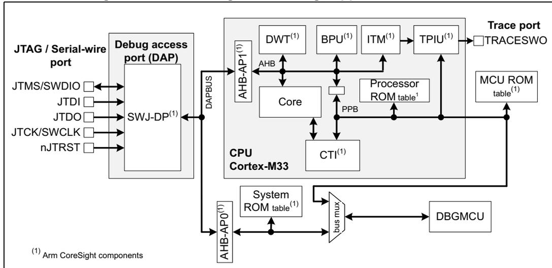
The diagram illustrates the internal architecture of the Cortex-M33 CPU and its debug support infrastructure. On the left, the 'Debug access port (DAP)' is shown with pins for JTAG/Serial-wire port (JTMS/SWDIO, JTDI, JTDO, JTCK/SWCLK, nJTRST) and a 'SWJ-DP (1) '. The DAP is connected to the 'DAPBUS'. The 'CPU Cortex-M33' core is connected to the 'DAPBUS' via 'AHB-AP1 (1) '. The core is also connected to 'DWT (1) ', 'BPU (1) ', 'ITM (1) ', and 'CTI (1) '. 'DWT (1) ', 'BPU (1) ', and 'ITM (1) ' are connected to 'TPIU (1) ', which outputs to the 'Trace port' (TRACESWO). 'CTI (1) ' is connected to the 'PPB' bus. The 'PPB' bus is also connected to 'Processor ROM table 1 ' and 'MCU ROM table (1) '. The 'PPB' bus is connected to a 'bus mux', which is connected to 'DBGMCU'. The 'bus mux' is also connected to 'System ROM table (1) '. The 'System ROM table (1) ' is connected to 'AHB-AP0 (1) ', which is connected to the 'DAPBUS'. A note at the bottom left indicates '(1) Arm CoreSight components'.
43.2.2 DBG pins and internal signals
Table 416. JTAG/Serial-wire debug port pins
| Pin name | JTAG debug port | Serial-wire debug port | Pin assignment | ||
|---|---|---|---|---|---|
| Type | Description | Type | Description | ||
| JTMS/SWDIO | I | JTAG test mode select | IO | Serial wire data in/out | PA13 |
| JTCK/SWCLK | I | JTAG test clock | I | Serial wire clock | PA14 |
| JTDI | I | JTAG test data input | - | - | PA15 |
| JTDO/TRACESWO (1) | O | JTAG test data output | - | - | PB3 |
| nJTRST | I | JTAG test reset | - | - | PB4 |
1. Debug access port JTDO and Trace port TRACESWO are multiplexed on a single device GPIO pin.
Table 417. Single-wire trace port pins
| Pin name | Type | Description | Pin assignment |
|---|---|---|---|
| TRACESWO | O | Single wire trace asynchronous data out | PB3 (1) |
1. TRACESWO is multiplexed with JTDO. This means that single-wire trace is only available when using the Serial-wire debug interface, and not when using JTAG.
43.2.3 DBG reset and clocks
The debug port (SWJ-DP) is reset by a power-on reset and when waking up from Standby mode.
The debugger supplies the clock for the debug port via the debug interface pin JTCK/SWCLK. This clock is used to register the serial input data in both Serial-wire and JTAG modes, as well as to operate the state machines and internal logic of the debug port. This clock must therefore continue to toggle for several cycles after the end of an access, to ensure that the debug port returns to the idle state.
The SWJ-DP contains an asynchronous interface to the DAPCLK domain, which covers the rest of the SWJ-DP.
The DAPCLK is a gated version of the CPU bus clock hclk1.
The DAPCLK domain is enabled by the debugger using the CDBGPWRUPREQ bit in the DP_CTRLSTATR register. The clock must be enabled before the debugger can access any of the debug features on the device. The availability of the clock is reflected in the CDBGPWRUPACK bit in the DP_CTRLSTATR register. DAPCLK is disabled at power up, after OBL, and after a wakeup from Standby. DAPCLK must be disabled when the debugger is disconnected to avoid wasting energy.
The debug components included in the processor are clocked with the processor core clock hclk1.
43.2.4 DBG power domains
The debug components are located in the core power domain. This means that debugger connection is not possible in Standby modes. To avoid losing the connection when the device enters Standby mode, the power to the core can be maintained by setting a bit in the debug unit (DBGMCU). This also keeps the processor clocks active and hold off the reset, so that the debug session is maintained.
43.2.5 DBG low-power modes
The devices include power saving features that allow the core power domain to be switched off or clocks to be stopped when not required. If the power is switched off all debug components are inaccessible to the debugger. When the core is not clocked all debug components except the DBGMCU are inaccessible to the debugger. To avoid this, low-power mode emulation is implemented. If emulation is enabled, the device still enters low-power mode, but the clocks and power are maintained. In other words, the device behaves similar as if it is in low-power mode, but the debugger does not lose the connection to the CPU.
The low-power emulation mode is programmed in the DBGMCU. For more information refer to Section 43.12.4: Low-power mode emulation .
43.2.6 DBG security
The trace and debug components allow a high degree of access to the processor and system during product development. In order to protect user code and ensure that the debug features can not be used to alter or compromise the normal operation of the finished product, these features can be disabled or limited in scope. For example, secure software debug and trace can be disabled without preventing the debug of non-secure code.
The following authentication signals are used by the device to determine which debug features are enabled or disabled:
- dbgen
: global enable for all debug features
0: All debug features are disabled.
1: Debug features in non-secure state are enabled. Debug features in secure state are dependent on the state of the spiden signal. - spiden
: enables debug in secure state when
dbgen
= 1.
0: Debug features are disabled in secure state.
1: Debug features are enabled in secure state. - niden
: enables trace and performance monitoring (non-invasive debug).
0: Trace generation is disabled.
1: Trace generation in non-secure state is enabled. Trace generation in secure state is dependent on the state of the spniden signal. - spniden
: enables trace and performance monitoring in secure state when
niden
= 1.
0: Trace generation is disabled in secure state.
1: Trace generation is enabled in secure state.
For detailed information on the behavior of each component according to the state of the authentication signals, refer to the relevant component chapter or to the relevant Arm® technical documentation.
The state of the signals are set according to the readout protection (RDP) level Readout protection (RDP), as shown in the following table.
Table 418. Debug features control
| RDP level | dbgen | spiden | niden | spniden | Description |
|---|---|---|---|---|---|
| 0 | 1 | 1 | 1 | 1 | Debug and trace is enabled whatever the state of the processor. The debugger access to secure memory is permitted. |
| 0.5 | Debug and trace is enabled when the processor is in non-secure state. The debugger access to secure memory is disabled. | ||||
| 1 | 1 | 0 | 1 | 0 | Debug and trace is enabled when the processor is in non-secure state. The debugger access to secure memory is disabled, as well as to the following areas: Flash memory, SRAM2, backup registers, ICACHE. |
| 2 | 0 | 0 | 0 | 0 | Debug and trace is disabled. |
Note: Security features are only relevant when option bit TZEN = 1. If security features are disabled, the authentication signals are still set according to the RDP level, but since the processor and all memories are non-secure, spniden and spiden are redundant.
The state of the authentication signals can be read from the DAUTHSTATUS register in the system control space (SCS) of the Cortex-M33.
The debugger access to secure areas (when permitted) must be performed using secure transactions from the AP, that is with the PROT[6] bit set in the AP_CSWR register.
The debugger access is disabled while the processor is booting from system Flash memory (RSS), whatever the RDP level.
43.2.7 Serial-wire and JTAG debug port
The Serial-wire and JTAG debug port (SWJ-DP) is a CoreSight component that implements an external access port for connecting debugging equipment.
The two following types of interface can be configured:
- • a 5-pin standard JTAG interface (JTAG-DP)
- • a 2-pin (clock + data) Serial-wire debug port (SW-DP)
The two modes are mutually exclusive since they share the same I/O pins.
By default the JTAG-DP is selected after a system or a power-on reset. The five I/O pins are configured by hardware in debug alternative function mode.
The SWJ-DP incorporates pull-up resistors on JTDI, JTMS/SWDIO and nJTRST, as well as a pull-down resistor on JTCK/SWCLK.
A debugger can select the SW-DP by transmitting the following serial data sequence on JTMS/SWDIO:
... (50 or more ones) ..., 0, 1, 1, 1, 1, 0, 0, 1, 1, 1, 1, 0, 0, 1, 1, 1, ... (50 or more ones) ...
JTCK/SWCLK must be cycled for each data bit.
In SW-DP mode, the unused JTAG pins JTDI, JTDO and nJTRST can be used for other functions.
Note: All SWJ port I/Os can be reconfigured to other functions by software but debugging is no longer possible.
43.2.8 JTAG debug port
The JTAG debug port (JTAG-DP) implements a TAP state machine (TAPSM) based on IEEE Std 1149.1-1990. The state machine controls two scan chains, one associated with an instruction register (IR) and the other one with a number of data registers (DR).
Figure 491. JTAG TAP state machine
The diagram illustrates the JTAG TAP state machine with the following states and transitions:
- Test-Logic-Reset : Initial state. Self-loop on JTMS=1. Transition to Run-Test/Idle on JTMS=0.
- Run-Test/Idle : State with self-loop on JTMS=0. Transitions to Select-DR-Scan and Select-IR-Scan on JTMS=1.
- Select-DR-Scan : Transition to Capture-DR on JTMS=0. Self-loop on JTMS=1.
- Capture-DR : Transition to Shift-DR on JTMS=0. Self-loop on JTMS=1.
- Shift-DR : Self-loop on JTMS=0. Transition to Exit1-DR on JTMS=1.
- Exit1-DR : Self-loop on JTMS=1. Transition to Pause-DR on JTMS=0.
- Pause-DR : Self-loop on JTMS=0. Transition to Exit2-DR on JTMS=1.
- Exit2-DR : Self-loop on JTMS=0. Transition to Update-DR on JTMS=1.
- Update-DR : Self-loop on JTMS=0. Transition to Run-Test/Idle on JTMS=1.
- Select-IR-Scan : Transition to Capture-IR on JTMS=0. Self-loop on JTMS=1.
- Capture-IR : Transition to Shift-IR on JTMS=0. Self-loop on JTMS=1.
- Shift-IR : Self-loop on JTMS=0. Transition to Exit1-IR on JTMS=1.
- Exit1-IR : Self-loop on JTMS=1. Transition to Pause-IR on JTMS=0.
- Pause-IR : Self-loop on JTMS=0. Transition to Exit2-IR on JTMS=1.
- Exit2-IR : Self-loop on JTMS=0. Transition to Update-IR on JTMS=1.
- Update-IR : Self-loop on JTMS=0. Transition to Run-Test/Idle on JTMS=1.
MSv60366V1
The operation of the JTAG-DP is as follows:
- 1. When the TAPSM goes through the Capture-IR state, 0b0001 is transferred onto the instruction register (IR) scan chain. The IR scan chain is connected between JTDI and JTDO.
- 2. While the TAPSM is in the Shift-IR state, the IR scan chain shifts one bit for each rising edge of JTCK. This means that, on the first tick:
- – The LSB of the IR scan chain is output on JTDO.
- – Bit[n] of the IR scan chain is transferred to bit[n-1].
- – The value on JTDI is transferred to the MSB of the IR scan chain.
- 3. When the TAPSM goes through the Update-IR state, the value scanned into the IR scan chain is transferred into the instruction register.
- 4. When the TAPSM goes through the Capture-DR state, a value is transferred from one of the data registers onto one of the DR scan chains, connected between JTDI and JTDO.
- 5. The value held in the instruction register determines which data register and associated DR scan chain are selected.
- 6. This data is then shifted while the TAPSM is in the Shift-DR state, in the same manner as the IR shift in the Shift-IR state.
- 7. When the TAPSM goes through the Update-DR state, the value scanned into the DR scan chain is transferred into the selected data register.
- 8. When the TAPSM is in the Run-Test/Idle state, no special actions occur. The IDCODE instruction is loaded in the instruction register.
When active, the nJTRST signal resets the state machine asynchronously to the Test-Logic-Reset state.
The data registers corresponding to the 4-bit IR instructions are listed in Table 419 .
Table 419. JTAG-DP data registers
| IR instruction | Data register | Scan chain length | Description |
|---|---|---|---|
| 0000 to 0111 | (BYPASS) | 1 | Not implemented: BYPASS selected |
| 1000 | ABORT | 35 | ABORT register – Bits 34:1 = Reserved – Bit 0 = APABORT: write 1 to generate an AP abort. |
| 1001 | (BYPASS) | 1 | Reserved: BYPASS selected |
| 1010 | DPACC | 35 | Debug port access register Initiates the debug port and gives access to a debug port register. – When transferring data IN: Bits 34:3 = DATA[31:0] = 32-bit data to transfer for a write request Bits 2:1 = A[3:2] = 2-bit address of a debug port register Bit 0 = RnW = Read request (1) or write request (0) – When transferring data OUT: Bits 34:3 = DATA[31:0] = 32-bit data read following a read request Bits 2:0 = ACK[2:0] = 3-bit Acknowledge 010 = OK/FAULT 001 = WAIT OTHER = reserved |
Table 419. JTAG-DP data registers (continued)
| IR instruction | Data register | Scan chain length | Description |
|---|---|---|---|
| 1011 | APACC | 35 | Access port access register Initiates an access port and gives access to an access port register. – When transferring data IN: Bits 34:3 = DATA[31:0] = 32-bit data to shift in for a write request Bits 2:1 = A[3:2] = 2-bit sub-address of an access port register Bit 0 = RnW= Read request (1) or write request (0) – When transferring data OUT: Bits 34:3 = DATA[31:0] = 32-bit data read following a read request Bits 2:0 = ACK[2:0] = 3-bit Acknowledge 010 = OK/FAULT 001 = WAIT OTHER = reserved |
| 1100 | (BYPASS) | 1 | Reserved: BYPASS selected |
| 1101 | (BYPASS) | 1 | Reserved: BYPASS selected |
| 1110 | IDCODE | 32 | ID code 0x0BA0 4477: Cortex-M33 JTAG debug port ID code |
| 1111 | BYPASS | 1 | Bypass A single JTAG cycle delay is inserted between JTDI and JTDO. |
Data registers are described in more detail in the Arm® Debug Interface Architecture Specification [1].
43.2.9 Serial-wire debug port
The Serial-wire debug (SWD) protocol uses the two following pins:
- • SWCLK: clock from host to target
- • SWDIO: bi-directional serial data
Serial data is transferred LSB first, synchronously with the clock.
A transfer comprises three phases:
- 1. packet request (8 bits) transmitted by the host (see Table 420 )
- 2. acknowledge response (3 bits) transmitted by the target (see Table 421 )
- 3. data transfer (33 bits) transmitted by the host (in case of a write) or target (in case of a read) (see Table 422 )
The data transfer only occurs if the acknowledge response is OK.
Between each phase, if the direction of the data is reversed, a single clock cycle turn-around time is inserted.
Table 420. Packet request
| Bit field | Name | Description |
|---|---|---|
| 0 | Start | Must be 1. |
| 1 | APnDP | – 0: DP register access - see
Table 419
for a list of DP registers – 1: AP register access - see Section 43.4: Access port |
| 2 | RnW | – 0: Write request – 1: Read request |
| 4:3 | A(3:2) | Address field of the DP or AP registers |
| 5 | Parity | Single bit parity of preceding bits |
| 6 | Stop | 0 |
| 7 | Park | Not driven by host, must be read as 1 by the target. |
Table 421. ACK response
| Bit field | Name | Description |
|---|---|---|
| 2:0 | ACK | – 000: FAULT – 010: WAIT – 100: OK |
Table 422. Data transfer
| Bit field | Name | Description |
|---|---|---|
| 31:0 | WDATA or RDATA | Write or read data |
| 32 | Parity | Single bit parity of 32 data bits |
In the case of a FAULT or WAIT ACK response from the target, the data transfer phase is canceled, unless overrun detection is enabled: in this case the data is ignored by the target (in the case of a write), or not driven (in the case of a read).
A line reset must be generated by the host when it is first connected, or following a protocol error. The line reset consists in 50 or more SWCLK cycles with SWDIO high, followed by two SWCLK cycles with SWDIO low.
For more details on the Serial-wire debug protocol, refer to the Arm® Debug Interface Architecture Specification [ 1 ].
Note: The SWJ-DP implements SWD protocol version 2.
43.3 Debug port registers
Both SW-DP and JTAG-DP access the debug port (DP) registers listed in Table 423 .
The debugger accesses the DP registers as follows:
- 1. Program the A(3:2) field in the DPACC register, if using JTAG, with the register address within the bank. Program the RnW bit to select a read or write. In the case of a write, program the DATA field with the write data. If using SWD, the A(3:2) and RnW fields
are part of the packet request word sent to the SW-DP with the APnDP bit reset (see Table 420 ). The write data are sent in the data phase.
- To access one of the banked DP registers at address 0x4, the register number must first be written to the DP_SELECTR register at address 0x8. Any subsequent read or write to address 0x4 accesses the register corresponding to the content of the DP_SELECTR register.
43.3.1 DP identification register [alternate] (DP_PIDR)
Address offset: 0x00
Reset value: 0x0BE0 2477 (SW-DP), 0x0BE0 1477 (JTAG-DP)
Read only
| 31 | 30 | 29 | 28 | 27 | 26 | 25 | 24 | 23 | 22 | 21 | 20 | 19 | 18 | 17 | 16 |
|---|---|---|---|---|---|---|---|---|---|---|---|---|---|---|---|
| REVISION[3:0] | PARTNO[7:0] | Res. | Res. | Res. | MIN | ||||||||||
| r | r | r | r | r | r | r | r | r | r | r | r | r | |||
| 15 | 14 | 13 | 12 | 11 | 10 | 9 | 8 | 7 | 6 | 5 | 4 | 3 | 2 | 1 | 0 |
| VERSION[3:0] | DESIGNER[10:0] | Res. | |||||||||||||
| r | r | r | r | r | r | r | r | r | r | r | r | r | r | r | |
Bits 31:28 REVISION[3:0] : Revision code
0x0 (JTAG-DP)
0x0 (SW-DP)
Bits 27:20 PARTNO[7:0] : Part number for the debug port
0xBE
Bits 19:17 Reserved, must be kept at reset value.
Bit 16 MIN : Minimal debug port (MINDP) implementation
0x1 MINDP not implemented (transaction counter and pushed operations are supported)
Bits 15:12 VERSION[3:0] : DP architecture version
0x1 (JTAG-DP)
0x2 (SW-DP)
Bits 11:1 DESIGNER[10:0] : JEDEC designer identity code
0x23B Arm ® JEDEC code
Bit 0 Reserved, must be kept at reset value.
43.3.2 DP abort register [alternate] (DP_ABORTR)
Address offset: 0x00
Reset value: 0x0000 0000
Write only
| 31 | 30 | 29 | 28 | 27 | 26 | 25 | 24 | 23 | 22 | 21 | 20 | 19 | 18 | 17 | 16 |
|---|---|---|---|---|---|---|---|---|---|---|---|---|---|---|---|
| Res. | Res. | Res. | Res. | Res. | Res. | Res. | Res. | Res. | Res. | Res. | Res. | Res. | Res. | Res. | Res. |
| 15 | 14 | 13 | 12 | 11 | 10 | 9 | 8 | 7 | 6 | 5 | 4 | 3 | 2 | 1 | 0 |
| Res. | Res. | Res. | Res. | Res. | Res. | Res. | Res. | Res. | Res. | Res. | ORUNERRCLR | WDERRCLR | STKERRCLR | Res. | DAPABORT |
| w | w | w | w |
Bits 31:5 Reserved, must be kept at reset value.
Bit 4 ORUNERRCLR : Overrun error clear
0: No effect
1: Clear STICKYORUN bit in DP_CTRLSTATR
Bit 3 WDERRCLR : Write data error clear
0: No effect
1: Clear WDATAERR bit in DP_CTRLSTATR
Bit 2 STKERRCLR : Sticky error clear
0: No effect
1: Clear STICKYERR bit in DP_CTRLSTATR
Bit 1 Reserved, must be kept at reset value.
Bit 0 DAPABORT : Data AP abort
Aborts current AP transaction if an excessive number of WAIT responses are returned, indicating that the transaction is stalled.
0: No effect
1: Aborts the transaction.
43.3.3 DP control and status register (DP_CTRLSTATR)
Address offset: 0x04
and DP_SELECTRL.DPBANKSEL = 0x0
Reset value: 0x0000 0000
| 31 | 30 | 29 | 28 | 27 | 26 | 25 | 24 | 23 | 22 | 21 | 20 | 19 | 18 | 17 | 16 |
|---|---|---|---|---|---|---|---|---|---|---|---|---|---|---|---|
| Res. | Res. | CDBGPWURUPACK | CDBGPWURUPREQ | Res. | Res. | Res. | Res. | Res. | Res. | Res. | Res. | Res. | Res. | Res. | Res. |
| r | rw | ||||||||||||||
| 15 | 14 | 13 | 12 | 11 | 10 | 9 | 8 | 7 | 6 | 5 | 4 | 3 | 2 | 1 | 0 |
| Res. | Res. | Res. | Res. | Res. | Res. | Res. | Res. | WDATAERR | READOK | STICKYERR | Res. | Res. | Res. | STICKYORUN | ORUNDETECT |
| r | r | rw | rw | rw |
Bits 31:30 Reserved, must be kept at reset value.
Bit 29 CDBGPWRUPACK : See description in Section 43.2.7
0 = DAPCLK gated
1 = DAPCLK enabled
Bit 28 CDBGPWRUPREQ : Control of DAPCLK enable request signal
0 = Requests DAPCLK gating
1 = Requests DAPCLK enabled
Bits 27:8 Reserved, must be kept at reset value.
Bit 7 WDATAERR : Write data error (read only) in SW-DP
There is a parity or framing error on the data phase of a write, or a write that has been accepted by the DP is then discarded without being submitted to the AP.
This bit is reset by writing 1 to the DP_ABORTR.WDERRCLR bit.
0: No error
1: An error occurred.
This bit is reserved in JTAG-DP.
Bit 6 READOK : AP read response (read only) in SW-DP
Indicates the response to the last AP read access.
0: Read not OK
1: Read OK
This bit is reserved in JTAG-DP.
Bit 5 STICKYERR : Transaction error (read only in SW-DP, R/W in JTAG-DP)
Indicates that an error occurred in an AP transaction.
0: No error
1: An error occurred.
In SW-DP, STICKYERR bit is read only, reset by writing 1 to the DP_ABORTR.STKERRCLR bit.
In JTAG-DP, STICKYERR bit is read, cleared by writing a 1 to it.
Bits 4:2 Reserved, must be kept at reset value.
Bit 1 STICKYORUN : Overrun (read only in SW-DP, R/W in JTAG-DP)
Indicates that an overrun occurred (new transaction received before previous transaction completed). This bit is only set if the ORUNDETECT bit is set.
0: No overrun
1: An overrun occurred.
In SW-DP, STICKYORUN bit is read only, reset by writing 1 to the DP_ABORTR.ORUNERRCLR bit.
In JTAG-DP, STICKYORUN bit is read, cleared by writing a 1 to it.
Bit 0 ORUNDETECT : Overrun detection mode enable
0: Overrun detection disabled
1: Overrun detection enabled
In the event of an overrun, the STICKYORUN bit is set and subsequent transactions are blocked until the STICKYORUN bit is cleared.
43.3.4 DP data link control register (DP_DLCR)
Address offset: 0x04
and DP_SELECTR.DPBANKSEL = 0x1
Reset value: 0x0000 0000
| 31 | 30 | 29 | 28 | 27 | 26 | 25 | 24 | 23 | 22 | 21 | 20 | 19 | 18 | 17 | 16 |
|---|---|---|---|---|---|---|---|---|---|---|---|---|---|---|---|
| Res. | Res. | Res. | Res. | Res. | Res. | Res. | Res. | Res. | Res. | Res. | Res. | Res. | Res. | Res. | Res. |
| 15 | 14 | 13 | 12 | 11 | 10 | 9 | 8 | 7 | 6 | 5 | 4 | 3 | 2 | 1 | 0 |
| Res. | Res. | Res. | Res. | Res. | Res. | TURNROUND [1:0] | WIREMODE [1:0] | Res. | Res. | Res. | Res. | Res. | Res. | ||
| r | r | r | r | ||||||||||||
Bits 31:10 Reserved, must be kept at reset value.
Bits 9:8 TURNROUND[1:0] : Tristate period for SWDIO
0x0: 1 data bit period
0x1: 2 data bit periods
0x2: 3 data bit periods
0x3: 4 data bit periods
Bits 7:6 WIREMODE[1:0] : SW-DP SWDIO
0x0: synchronous
others: reserved
Bits 5:0 Reserved, must be kept at reset value.
43.3.5 DP target identification register (DP_TARGETIDR)
Address offset: 0x04
and DP_SELECTR.DPBANKSEL = 0x2
Reset value: 0x0492 0041
| 31 | 30 | 29 | 28 | 27 | 26 | 25 | 24 | 23 | 22 | 21 | 20 | 19 | 18 | 17 | 16 |
|---|---|---|---|---|---|---|---|---|---|---|---|---|---|---|---|
| TREVISION[3:0] | TPARTNO[15:4] | ||||||||||||||
| r | r | r | r | r | r | r | r | r | r | r | r | r | r | r | r |
| 15 | 14 | 13 | 12 | 11 | 10 | 9 | 8 | 7 | 6 | 5 | 4 | 3 | 2 | 1 | 0 |
| TPARTNO[3:0] | TDESIGNER[10:0] | Res. | |||||||||||||
| r | r | r | r | r | r | r | r | r | r | r | r | r | r | r | |
Bits 31:28 TREVISION[3:0] : Target revision
0x0: revision A
Bits 27:12 TPARTNO[15:0] : Target part number
0x4920: STM32WBA5xxx
Bits 11:1 TDESIGNER[10:0] : Target designer JEDEC code.
0x020: STMicroelectronics
Bit 0 Reserved, must be kept at reset value.
43.3.6 DP data link protocol identification register (DP_DLPIDR)
Address offset: 0x04
and DP_SELECTR.DPBANKSEL = 0x3
Reset value: 0x0000 0001
| 31 | 30 | 29 | 28 | 27 | 26 | 25 | 24 | 23 | 22 | 21 | 20 | 19 | 18 | 17 | 16 |
|---|---|---|---|---|---|---|---|---|---|---|---|---|---|---|---|
| TINSTANCE[3:0] | Res. | Res. | Res. | Res. | Res. | Res. | Res. | Res. | Res. | Res. | Res. | Res. | |||
| r | r | r | r | ||||||||||||
| 15 | 14 | 13 | 12 | 11 | 10 | 9 | 8 | 7 | 6 | 5 | 4 | 3 | 2 | 1 | 0 |
| Res. | Res. | Res. | Res. | Res. | Res. | Res. | Res. | Res. | Res. | Res. | Res. | PROTSVN[3:0] | |||
| r | r | r | r | ||||||||||||
Bits 31:28 TINSTANCE[3:0] : Target instance number
Defines the instance number for this device in a multi-drop system.
0x0: Instance number 0
Bits 27:4 Reserved, must be kept at reset value.
Bits 3:0 PROTSVN[3:0] : Serial-wire debug protocol version
0x1: Version 2
43.3.7 DP resend register (DP_EVENSTRR)
Address offset: 0x04
and DP_SELECTR.DPBANKSEL = 0x4
Reset value: 0x0000 0001
| 31 | 30 | 29 | 28 | 27 | 26 | 25 | 24 | 23 | 22 | 21 | 20 | 19 | 18 | 17 | 16 |
|---|---|---|---|---|---|---|---|---|---|---|---|---|---|---|---|
| Res. | Res. | Res. | Res. | Res. | Res. | Res. | Res. | Res. | Res. | Res. | Res. | Res. | Res. | Res. | Res. |
| 15 | 14 | 13 | 12 | 11 | 10 | 9 | 8 | 7 | 6 | 5 | 4 | 3 | 2 | 1 | 0 |
| Res. | Res. | Res. | Res. | Res. | Res. | Res. | Res. | Res. | Res. | Res. | Res. | Res. | Res. | Res. | EA |
| r |
Bits 31:1 Reserved, must be kept at reset value.
Bit 0 EA : Event status flag
0: Cortex-M33 processor halted
1: Cortex-M33 processor not halted.
43.3.8 DP resend register (DP_RESENR)
Address offset: 0x08
Reset value: 0x0000 0000
| 31 | 30 | 29 | 28 | 27 | 26 | 25 | 24 | 23 | 22 | 21 | 20 | 19 | 18 | 17 | 16 |
| RESEND[31:16] | |||||||||||||||
| r | r | r | r | r | r | r | r | r | r | r | r | r | r | r | r |
| 15 | 14 | 13 | 12 | 11 | 10 | 9 | 8 | 7 | 6 | 5 | 4 | 3 | 2 | 1 | 0 |
| RESEND[15:0] | |||||||||||||||
| r | r | r | r | r | r | r | r | r | r | r | r | r | r | r | r |
Bits 31:0
RESEND[31:0]
: Value returned by the last AP read or DP_RDBUFR read.
Used in the event of a corrupted read transfer.
43.3.9 DP access port select register (DP_SELECTR)
Address offset: 0x08
Reset value: 0xXXXX XXXX
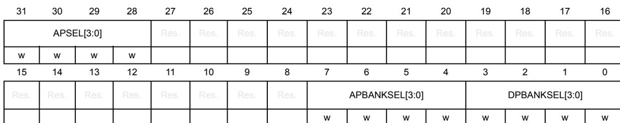
| 31 | 30 | 29 | 28 | 27 | 26 | 25 | 24 | 23 | 22 | 21 | 20 | 19 | 18 | 17 | 16 |
| APSEL[3:0] | Res. | Res. | Res. | Res. | Res. | Res. | Res. | Res. | Res. | Res. | Res. | Res. | |||
| w | w | w | w | ||||||||||||
| 15 | 14 | 13 | 12 | 11 | 10 | 9 | 8 | 7 | 6 | 5 | 4 | 3 | 2 | 1 | 0 |
| Res. | Res. | Res. | Res. | Res. | Res. | Res. | Res. | APBANKSEL[3:0] | DPBANKSEL[3:0] | ||||||
| w | w | w | w | w | w | w | w | ||||||||
Bits 31:28 APSEL[3:0] : Access port selection
Selects the access port for the next transaction.
0x0: AP0 - System debug access port
0x1: AP1 - Cortex-M33 debug access port
others: reserved
Bits 27:8 Reserved, must be kept at reset value.
Bits 7:4 APBANKSEL[3:0] : AP register bank selection
Selects the 4-word register bank on the active AP for the next transaction.
Bits 3:0 DPBANKSEL[3:0] : DP register bank selection
Selects the register at address 0x4 of the debug port.
0x0: DP_CTRLSTATR
0x1: DP_DLCR
0x2: DP_TARGETIDR
0x3: DP_DLPIDR
0x4: DP_EVENTSTAT
others: reserved
43.3.10 DP read buffer register (DP_BUFFR)
Address offset: 0x0C
Reset value: 0x0000 0000
| 31 | 30 | 29 | 28 | 27 | 26 | 25 | 24 | 23 | 22 | 21 | 20 | 19 | 18 | 17 | 16 |
| RDBUFF[31:16] | |||||||||||||||
| r | r | r | r | r | r | r | r | r | r | r | r | r | r | r | r |
| 15 | 14 | 13 | 12 | 11 | 10 | 9 | 8 | 7 | 6 | 5 | 4 | 3 | 2 | 1 | 0 |
| RDBUFF[15:0] | |||||||||||||||
| r | r | r | r | r | r | r | r | r | r | r | r | r | r | r | r |
Bits 31:0 RDBUFF[31:0] : Contains the value returned by the last AP read access.
The value returned by an AP read access can either be obtained using a second read access to the same address, which initiates a new transaction on the corresponding bus, or else it can be read from this register, in which case no new AP transaction occurs.
43.3.11 DP register map and reset values
These registers are not on the CPU memory bus and are accessed only through SW-DP and JTAG-DP debug interface.
The debug port address is 2-bit wide, defined in the JTAG-DP register DPACC or SW-DP packet request A[3:2] field.
Table 423. DP register map and reset values
| Offset | Register name | 31 | 30 | 29 | 28 | 27 | 26 | 25 | 24 | 23 | 22 | 21 | 20 | 19 | 18 | 17 | 16 | 15 | 14 | 13 | 12 | 11 | 10 | 9 | 8 | 7 | 6 | 5 | 4 | 3 | 2 | 1 | 0 |
|---|---|---|---|---|---|---|---|---|---|---|---|---|---|---|---|---|---|---|---|---|---|---|---|---|---|---|---|---|---|---|---|---|---|
| 0x00 | DP_DPIDR | REVISION[3:0] | PARTNO[7:0] | Res. | Res. | Res. | MIN | VERSION[3:0] | DESIGNER[10:0] | Res. | |||||||||||||||||||||||
| Reset value | 0 | 0 | 0 | 0 | 1 | 0 | 1 | 1 | 1 | 1 | 1 | 0 | 0 | X | X | X | X | 0 | 1 | 0 | 0 | 0 | 1 | 1 | 1 | 0 | 1 | 1 | |||||
| 0x00 | DP_ABORTR | Res. | Res. | Res. | Res. | Res. | Res. | Res. | Res. | Res. | Res. | Res. | Res. | Res. | Res. | Res. | Res. | Res. | Res. | Res. | Res. | Res. | Res. | Res. | Res. | Res. | Res. | Res. | ORUNERRCLR | WDERRCLR | STKERRCLR | Res. | DAPABORT |
| Reset value | 0 | 0 | 0 | 0 | |||||||||||||||||||||||||||||
| 0x04 (1) | DP_CTRLSTATR | Res. | Res. | CDBGPWURUPACK | CDBGPWURUPREQ | Res. | Res. | Res. | Res. | Res. | Res. | Res. | Res. | Res. | Res. | Res. | Res. | Res. | Res. | Res. | Res. | Res. | Res. | Res. | WDATAERR | READOK | STICKYERR | Res. | Res. | Res. | Res. | STICKYORUN | ORUNDETECT |
| Reset value | 0 | 0 | 0 | 0 | 0 | 0 | 0 | ||||||||||||||||||||||||||
| 0x04 (2) | DP_DLCR | Res. | Res. | Res. | Res. | Res. | Res. | Res. | Res. | Res. | Res. | Res. | Res. | Res. | Res. | Res. | Res. | Res. | Res. | Res. | Res. | Res. | Res. | TURNROUND[1:0] | WIREMODE[1:0] | Res. | Res. | Res. | Res. | Res. | Res. | ||
| Reset value | 0 | 0 | 0 | 0 | |||||||||||||||||||||||||||||
| Offset | Register name | 31 | 30 | 29 | 28 | 27 | 26 | 25 | 24 | 23 | 22 | 21 | 20 | 19 | 18 | 17 | 16 | 15 | 14 | 13 | 12 | 11 | 10 | 9 | 8 | 7 | 6 | 5 | 4 | 3 | 2 | 1 | 0 |
|---|---|---|---|---|---|---|---|---|---|---|---|---|---|---|---|---|---|---|---|---|---|---|---|---|---|---|---|---|---|---|---|---|---|
| 0x04 (3) | DP_TARGETIDR | TREVISION[3:0] | TPARTNO[15:0] | TDESIGNER[10:0] | Res. | ||||||||||||||||||||||||||||
| Reset value | 0 | 0 | 0 | 0 | 0 | 1 | 0 | 0 | 1 | 0 | 0 | 1 | 0 | 0 | 1 | 0 | 0 | 0 | 0 | 0 | 0 | 0 | 0 | 0 | 0 | 1 | 0 | 0 | 0 | 0 | 0 | 0 | |
| 0x04 (4) | DP_DLPIDR | TINSTANCE[3:0] | Res. | PROTSVN[3:0] | |||||||||||||||||||||||||||||
| Reset value | 0 | 0 | 0 | 0 | 0 | 0 | 0 | 1 | |||||||||||||||||||||||||
| 0x04 (5) | DP_EVENTSTATR | Res. | EA | ||||||||||||||||||||||||||||||
| Reset value | 0 | ||||||||||||||||||||||||||||||||
| 0x08 | DP_RESENDR | RESEND[31:0] | |||||||||||||||||||||||||||||||
| Reset value | 0 | 0 | 0 | 0 | 0 | 0 | 0 | 0 | 0 | 0 | 0 | 0 | 0 | 0 | 0 | 0 | 0 | 0 | 0 | 0 | 0 | 0 | 0 | 0 | 0 | 0 | 0 | 0 | 0 | 0 | 0 | 0 | |
| 0x08 | DP_SELECTR | APSEL[3:0] | Res. | APBANKSEL[3:0] | DPBANKSEL[3:0] | ||||||||||||||||||||||||||||
| Reset value | X | X | X | X | X | X | X | X | X | X | X | X | |||||||||||||||||||||
| 0x0C | DP_BUFFR | RDBUFF[31:0] | |||||||||||||||||||||||||||||||
| Reset value | 0 | 0 | 0 | 0 | 0 | 0 | 0 | 0 | 0 | 0 | 0 | 0 | 0 | 0 | 0 | 0 | 0 | 0 | 0 | 0 | 0 | 0 | 0 | 0 | 0 | 0 | 0 | 0 | 0 | 0 | 0 | 0 | |
- 1. DP_SELECTR.DPBANKSEL = 0x0.
- 2. DP_SELECTR.DPBANKSEL = 0x1.
- 3. DP_SELECTR.DPBANKSEL = 0x2.
- 4. DP_SELECTR.DPBANKSEL = 0x3.
- 5. DP_SELECTR.DPBANKSEL = 0x4
Refer to Section 43.3: Debug port registers for the register boundary addresses.
43.4 Access port
There are two access ports (AP) attached to the DP.
- • AP0, System debug access port: enables access to the system debug features integrated at device level.
- • AP1, Cortex-M33 processor core access port: enables access to the debug and trace features integrated in the Cortex-M33 processor core.
43.4.1 Access port registers
The access ports are of MEM-AP type: the debug and trace component registers are mapped in the address space of the associated bus.
An AP is seen by the debugger as a set of 32-bit registers organized in banks of four registers each. Some of these registers are used to configure or monitor the AP itself, while others are used to perform a transfer on the bus. The AP registers are listed in Table 424 .
The address of the AP registers is composed of the following fields:
- • Bits [7:4]: content of the APBANKSEL[3:0] field in the DP_SELECTR register
- • Bits [3:2]: content of the A(3:2) field of the APACC data register in the JTAG-DP or of the SW-DP packet request, depending on the debug interface used
- • Bits [1:0]: always set to 0
The content of the APSEL[3:0] defines which MEM-AP is being accessed.
The debugger can access the AP registers as follows:
- 1. Program in the APSEL[3:0] field to choose the AP and the APBANKSEL[3:0] field to select the register bank to be accessed.
- 2. Program the A(3:2) field in the APACC register, if using JTAG, with the register address within the bank. Program the RnW bit to select a read or write. In the case of a write, program the DATA field with the write data. If using SWD, the A(3:2) and RnW fields are part of the packet request word sent to the SW-DP with the APnDP bit set (see Table 420 ). The write data is sent in the data phase.
The debugger can access the memory mapped debug component registers through the MEM-AP registers (using the above AP register access procedure) as follows:
- 1. Program the transaction target address in the AP_TAR register.
- 2. Program the AP_CSWR register, if necessary, with the transfer parameters (AddrInc for example).
- 3. Write to or read from the AP_DRWR register to initiate a bus transaction at the address held in the AP_TAR register. Alternatively, a read or write to the AP_BDxR register triggers an access to address \( AP\_TAR[31:4] + x \) (allowing up to four consecutive addresses to be accessed without changing the address in the AP_TAR register).
For more detailed information on the MEM-AP, refer to the Arm® Debug Interface Architecture Specification [1] .
43.4.2 AP control/status word register (APx_CSWR) (x = 0 to 1)
Address offset: 0x00
Reset value: 0x0100 00X0
| 31 | 30 | 29 | 28 | 27 | 26 | 25 | 24 | 23 | 22 | 21 | 20 | 19 | 18 | 17 | 16 |
|---|---|---|---|---|---|---|---|---|---|---|---|---|---|---|---|
| Res. | PROT6 | Res. | Res. | PROT[3:0] | Res. | Res. | Res. | Res. | Res. | Res. | Res. | Res. | |||
| rw | rw | rw | rw | r | |||||||||||
| 15 | 14 | 13 | 12 | 11 | 10 | 9 | 8 | 7 | 6 | 5 | 4 | 3 | 2 | 1 | 0 |
| Res. | Res. | Res. | Res. | Res. | Res. | Res. | Res. | Res. | DBG STATUS | ADDRINC[1:0] | Res. | SIZE[2:0] | |||
| r | rw | rw | rw | rw | rw | ||||||||||
Bit 31 Reserved, must be kept at reset value.
Bit 30 PROT6 : Secure transfer protection bit [6]
This field sets protection attribute HPROT[6] of the AP bus transfer.
0: secure transfer
1: non-secure transfer
Bits 29:28 Reserved, must be kept at reset value.
Bits 27:24 PROT[3:0] : Bus transfer protection
This field sets protection attribute HPROT[3:0] of the AP bus transfer.
0bXXX1: data transfer
0bXX0X: unprivileged transfer
0bXX1X: privileged transfer
0bX0XX: non-bufferable
0bX1XX: bufferable
0b0XXX: non-shareable, no look-up non-modifiable
0b1XXX: sharable, look-up, modifiable
Bits 23:7 Reserved, must be kept at reset value.
Bit 6 DBGSTATUS : Device enable (DEVICEEN) status
Indicates whether the Cortex-M33 AP bus can be accessed by the debugger. This bit reflects the state of dbgen.
0: AP AHB bus transfers blocked.
1: AP AHB bus transfers granted.
Bits 5:4 ADDRINC[1:0] : Auto-increment mode
Defines whether AP_TAR address is automatically incremented after a transaction.
0x0: No auto-increment
0x1: Address is incremented by the size in bytes of the transaction (SIZE field).
others: reserved
Bit 3 Reserved, must be kept at reset value.
Bits 2:0 SIZE[2:0] : Size of next memory access transaction
0x0: byte (8-bit)
0x1: halfword (16-bit)
0x2: word (32-bit)
others: reserved
43.4.3 AP transfer address register (APx_TAR) (x = 0 to 1)
Address offset: 0x04
Reset value: 0xXXXX XXXX
| 31 | 30 | 29 | 28 | 27 | 26 | 25 | 24 | 23 | 22 | 21 | 20 | 19 | 18 | 17 | 16 |
| TA[31:16] | |||||||||||||||
| rw | rw | rw | rw | rw | rw | rw | rw | rw | rw | rw | rw | rw | rw | rw | rw |
| 15 | 14 | 13 | 12 | 11 | 10 | 9 | 8 | 7 | 6 | 5 | 4 | 3 | 2 | 1 | 0 |
| TA[15:0] | |||||||||||||||
| rw | rw | rw | rw | rw | rw | rw | rw | rw | rw | rw | rw | rw | rw | rw | rw |
Bits 31:0 TA[31:0] : Address of current transfer
43.4.4 AP data read/write register (APx_DRWR) (x = 0 to 1)
Address offset: 0x0C
Reset value: 0xXXXX XXXX
| 31 | 30 | 29 | 28 | 27 | 26 | 25 | 24 | 23 | 22 | 21 | 20 | 19 | 18 | 17 | 16 |
| TD[31:16] | |||||||||||||||
| rw | rw | rw | rw | rw | rw | rw | rw | rw | rw | rw | rw | rw | rw | rw | rw |
| 15 | 14 | 13 | 12 | 11 | 10 | 9 | 8 | 7 | 6 | 5 | 4 | 3 | 2 | 1 | 0 |
| TD[15:0] | |||||||||||||||
| rw | rw | rw | rw | rw | rw | rw | rw | rw | rw | rw | rw | rw | rw | rw | rw |
Bits 31:0 TD[31:0] : Data of current transfer
43.4.5 AP banked data registers y (APx_BDyR) (x = 0 to 1)
Address offset: 0x10 + 0x4 * y, (y = 0 to 3)
Reset value: 0x0000 0000
| 31 | 30 | 29 | 28 | 27 | 26 | 25 | 24 | 23 | 22 | 21 | 20 | 19 | 18 | 17 | 16 |
| TBD[31:16] | |||||||||||||||
| rw | rw | rw | rw | rw | rw | rw | rw | rw | rw | rw | rw | rw | rw | rw | rw |
| 15 | 14 | 13 | 12 | 11 | 10 | 9 | 8 | 7 | 6 | 5 | 4 | 3 | 2 | 1 | 0 |
| TBD[15:0] | |||||||||||||||
| rw | rw | rw | rw | rw | rw | rw | rw | rw | rw | rw | rw | rw | rw | rw | rw |
Bits 31:0
TBD[31:0]
: Banked data of current transfer to address in AP_TAR
AP_TAR + AP_BDnR address [3:2] + 0b00
The auto address incrementing is not performed on AP_BD[3:0]R.
Banked transfers are only supported for word transfers.
43.4.6 AP configuration register (APx_CFGR) (x = 0 to 1)
Address offset: 0xF4
Reset value: 0x0000 0000
| 31 | 30 | 29 | 28 | 27 | 26 | 25 | 24 | 23 | 22 | 21 | 20 | 19 | 18 | 17 | 16 |
|---|---|---|---|---|---|---|---|---|---|---|---|---|---|---|---|
| Res. | Res. | Res. | Res. | Res. | Res. | Res. | Res. | Res. | Res. | Res. | Res. | Res. | Res. | Res. | Res. |
| 15 | 14 | 13 | 12 | 11 | 10 | 9 | 8 | 7 | 6 | 5 | 4 | 3 | 2 | 1 | 0 |
| Res. | Res. | Res. | Res. | Res. | Res. | Res. | Res. | Res. | Res. | Res. | Res. | Res. | LD | LA | BE |
| r | r | r |
Bits 31:3 Reserved, must be kept at reset value.
Bit 2 LD : Large data
0: Data not longer than 32-bits supported.
Bit 1 LA : Long address
0: Physical addresses not longer than 32-bits supported.
Bit 0 BE : Big-endian
0: only little-endian supported.
43.4.7 AP base address register (APx_BASER) (x = 0 to 1)
Address offset: 0xF8
Reset value: Block 0: 0xE008 0003
Reset value: Block 1: 0xE00F E003
| 31 | 30 | 29 | 28 | 27 | 26 | 25 | 24 | 23 | 22 | 21 | 20 | 19 | 18 | 17 | 16 |
|---|---|---|---|---|---|---|---|---|---|---|---|---|---|---|---|
| BASEADDR[31:16] | |||||||||||||||
| r | r | r | r | r | r | r | r | r | r | r | r | r | r | r | r |
| 15 | 14 | 13 | 12 | 11 | 10 | 9 | 8 | 7 | 6 | 5 | 4 | 3 | 2 | 1 | 0 |
| BASEADDR[15:12] | Res. | Res. | Res. | Res. | Res. | Res. | Res. | Res. | Res. | Res. | FORMAT | ENTRY PRESENT | |||
| r | r | r | r | r | r | ||||||||||
Bits 31:12 BASEADDR[31:12] : Base address (bits 31 to 12) of ROM table for the AP
The 12 LSBs are zero since the ROM table must be aligned on a 4-Kbyte boundary.
AP0: 0xE0080 (system ROM table)
AP1: 0xE00FE (MCU ROM table)
Bits 11:2 Reserved, must be kept at reset value.
Bit 1 FORMAT : Base address register format
1: Arm ® debug interface v5
Bit 0 ENTRYPRESENT : Debug components presence
Indicates that debug components are present on the access port bus.
1: debug components are present
43.4.8 AP identification register (APx_IDR) (x = 0 to 1)
Address offset: 0xFC
Reset value: 0x1477 0015
| 31 | 30 | 29 | 28 | 27 | 26 | 25 | 24 | 23 | 22 | 21 | 20 | 19 | 18 | 17 | 16 |
|---|---|---|---|---|---|---|---|---|---|---|---|---|---|---|---|
| REVISION[3:0] | JEDECBANK[3:0] | JEDECCODE[6:0] | CLASS[3] | ||||||||||||
| r | r | r | r | r | r | r | r | r | r | r | r | r | r | r | r |
| 15 | 14 | 13 | 12 | 11 | 10 | 9 | 8 | 7 | 6 | 5 | 4 | 3 | 2 | 1 | 0 |
| CLASS[2:0] | Res. | Res. | Res. | Res. | Res. | VARIANT[3:0] | TYPE[3:0] | ||||||||
| r | r | r | r | r | r | r | r | r | r | r | |||||
Bits 31:28 REVISION[3:0] : Revision
0x1: r0p1
Bits 27:24 JEDECBANK[3:0] : JEDEC bank
0x4: Arm ®
Bits 23:17 JEDECCODE[6:0] : JEDEC code
0x3B: Arm ®
Bits 16:13 CLASS[3:0] : Memory access port
0x8: MEM_AP Standard register map
Bits 12:8 Reserved, must be kept at reset value.
Bits 7:4 VARIANT[3:0] : AP variant
0x1: AHB-AP
Bits 3:0 TYPE[3:0] : AP type
0x5: AHB5
43.4.9 Access port register map and reset values
These registers are not on the CPU memory bus and are only accessed through SW-DP and JTAG-DP debug interface.
The access port address is 8-bit wide, defined by DP_SELECTR.APBANKSEL[3:0] field and by JTAG-DP register DPACC or SW-DP packet request A[3:2] field.
Table 424. AP register map and reset values
| Offset | Register name | 31 | 30 | 29 | 28 | 27 | 26 | 25 | 24 | 23 | 22 | 21 | 20 | 19 | 18 | 17 | 16 | 15 | 14 | 13 | 12 | 11 | 10 | 9 | 8 | 7 | 6 | 5 | 4 | 3 | 2 | 1 | 0 |
|---|---|---|---|---|---|---|---|---|---|---|---|---|---|---|---|---|---|---|---|---|---|---|---|---|---|---|---|---|---|---|---|---|---|
| 0x00 | AP1_CSWR | Res. | SPROT[6] | Res. | Res. | PROT[3:0] | Res. | Res. | Res. | Res. | Res. | Res. | Res. | Res. | Res. | Res. | Res. | Res. | Res. | Res. | Res. | Res. | Res. | DBGSTATUS | ADDRINC[1:0] | Res. | SIZE[2:0] | ||||||
| Reset value | 0 | 0 | 0 | 0 | 1 | X | 0 | 0 | 0 | 0 | 0 | ||||||||||||||||||||||
| 0x04 | APx_TAR | TA[31:0] | |||||||||||||||||||||||||||||||
| Reset value | 0 | 0 | 0 | 0 | 0 | 0 | 0 | 0 | 0 | 0 | 0 | 0 | 0 | 0 | 0 | 0 | 0 | 0 | 0 | 0 | 0 | 0 | 0 | 0 | 0 | 0 | 0 | 0 | 0 | 0 | 0 | 0 | |
| 0x08 | Reserved | Reserved | |||||||||||||||||||||||||||||||
| 0x0C | APx_DRWR | TD[31:0] | |||||||||||||||||||||||||||||||
| Reset value | 0 | 0 | 0 | 0 | 0 | 0 | 0 | 0 | 0 | 0 | 0 | 0 | 0 | 0 | 0 | 0 | 0 | 0 | 0 | 0 | 0 | 0 | 0 | 0 | 0 | 0 | 0 | 0 | 0 | 0 | 0 | 0 | |
| 0x10 | APx_BD0R | TBD[31:0] | |||||||||||||||||||||||||||||||
| Reset value | 0 | 0 | 0 | 0 | 0 | 0 | 0 | 0 | 0 | 0 | 0 | 0 | 0 | 0 | 0 | 0 | 0 | 0 | 0 | 0 | 0 | 0 | 0 | 0 | 0 | 0 | 0 | 0 | 0 | 0 | 0 | 0 | |
| 0x14 | APx_BD1R | TBD[31:0] | |||||||||||||||||||||||||||||||
| Reset value | 0 | 0 | 0 | 0 | 0 | 0 | 0 | 0 | 0 | 0 | 0 | 0 | 0 | 0 | 0 | 0 | 0 | 0 | 0 | 0 | 0 | 0 | 0 | 0 | 0 | 0 | 0 | 0 | 0 | 0 | 0 | 0 | |
| 0x18 | APx_BD2R | TBD[31:0] | |||||||||||||||||||||||||||||||
| Reset value | 0 | 0 | 0 | 0 | 0 | 0 | 0 | 0 | 0 | 0 | 0 | 0 | 0 | 0 | 0 | 0 | 0 | 0 | 0 | 0 | 0 | 0 | 0 | 0 | 0 | 0 | 0 | 0 | 0 | 0 | 0 | 0 | |
| 0x1C | APx_BD3R | TBD[31:0] | |||||||||||||||||||||||||||||||
| Reset value | 0 | 0 | 0 | 0 | 0 | 0 | 0 | 0 | 0 | 0 | 0 | 0 | 0 | 0 | 0 | 0 | 0 | 0 | 0 | 0 | 0 | 0 | 0 | 0 | 0 | 0 | 0 | 0 | 0 | 0 | 0 | 0 | |
| 0x20 to 0xF0 | Reserved | Reserved | |||||||||||||||||||||||||||||||
| 0xF4 | APx_CFGR | Res. | Res. | Res. | Res. | Res. | Res. | Res. | Res. | Res. | Res. | Res. | Res. | Res. | Res. | Res. | Res. | Res. | Res. | Res. | Res. | Res. | Res. | Res. | Res. | Res. | Res. | Res. | Res. | Res. | LD | LA | BE |
| Reset value | 0 | 0 | 0 | ||||||||||||||||||||||||||||||
| 0xF8 | AP0_BASER | BASEADDR[31:12] | Res. | Res. | Res. | Res. | Res. | Res. | Res. | Res. | Res. | Res. | Res. | FORMAT | ENTRYPRESENT | ||||||||||||||||||
| Reset value | 1 | 1 | 1 | 0 | 0 | 0 | 0 | 0 | 0 | 0 | 0 | 0 | 1 | 0 | 0 | 0 | 0 | 0 | 0 | 1 | 1 | ||||||||||||
| 0xF8 | AP1_BASER | BASEADDR[31:12] | Res. | Res. | Res. | Res. | Res. | Res. | Res. | Res. | Res. | Res. | Res. | FORMAT | ENTRYPRESENT | ||||||||||||||||||
| Reset value | 1 | 1 | 1 | 0 | 0 | 0 | 0 | 0 | 0 | 0 | 0 | 0 | 1 | 1 | 1 | 1 | 1 | 1 | 1 | 0 | 1 | 1 | |||||||||||
| 0xFC | APx_IDR | REVISION [3:0] | JEDECBANK [3:0] | JEDECCODE[6:0] | CLASS[3:0] | Res. | Res. | Res. | Res. | Res. | VARIANT[3:0] | TYPE[3:0] | |||||||||||||||||||||
| Reset value | 0 | 0 | 0 | 1 | 0 | 1 | 0 | 0 | 0 | 1 | 1 | 1 | 0 | 1 | 1 | 1 | 0 | 0 | 0 | 0 | 0 | 1 | 0 | 1 | 0 | 1 | |||||||
43.5 System debug AP0 features
The system debug subsystem integrates the following features accessible through the AP0:
- • system ROM table
- • debug MCU controller (DBGMCU)
43.5.1 System debug ROM table
The system debug ROM table is a CoreSight component that contains the base addresses of all the debug components accessible via the AP0. This table allows a debugger to discover the topology of the debug system automatically.
There is one ROM table in the system debug sub-system.
- 1. The system debug ROM table is pointed to by the AP0_BASER register. It contains the base-address pointer for the DBGMCU.
The system debug ROM table (see Table 425 ) occupies a 4-Kbyte, 32-bit wide chunk of address space, from 0xE008 0000 to 0xE008 0FFC.
Table 425. System debug ROM table
| Address offset in ROM table | Component name | Component base address | Component address offset | Size (Kbytes) | Entry |
|---|---|---|---|---|---|
| 0x000 | DBGMCU | 0xE004 4000 | 0xFFFC 4000 | 4 | 0xFFFC 4003 |
| 0x004 | Top of table | - | - | - | 0x0000 0000 |
| 0x00C to 0xFC8 | Reserved | - | - | - | 0x0000 0000 |
| 0xFCC to 0xFFC | ROM table registers | - | - | - | See Table 429 |
The CoreSight topology for the debug components in the system debug sub-system is shown in Figure 492 .
Figure 492. AP0: CoreSight topology
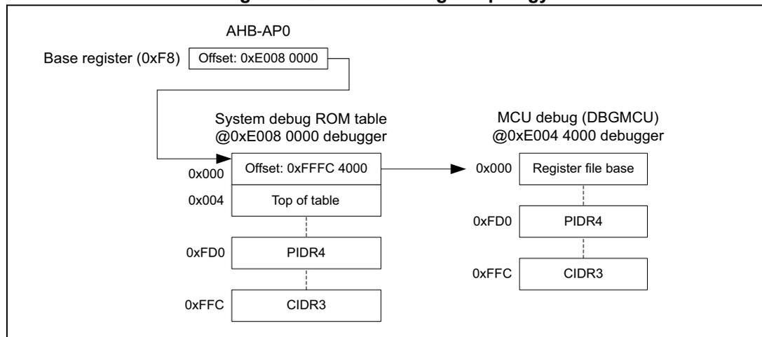
The diagram illustrates the CoreSight topology for the debug components in the system debug sub-system. At the top, the AHB-AP0 base register (0xF8) is shown with an offset of 0xE008 0000. This register points to the System debug ROM table located at 0xE008 0000. The ROM table contains entries for the MCU debug (DBGMCU) component at 0xE004 4000. The DBGMCU component includes a register file base at 0x000, PIDR4 at 0xFD0, and CIDR3 at 0xFFC. The ROM table itself contains entries for the DBGMCU component at 0x000 (Offset: 0xFFFC 4000), Top of table at 0x004, PIDR4 at 0xFD0, and CIDR3 at 0xFFC.
43.5.2 System debug memory type register (SYSROM_MEMTYPER)
Address offset: 0xFCC
Reset value: 0x0000 0000
| 31 | 30 | 29 | 28 | 27 | 26 | 25 | 24 | 23 | 22 | 21 | 20 | 19 | 18 | 17 | 16 |
|---|---|---|---|---|---|---|---|---|---|---|---|---|---|---|---|
| Res. | Res. | Res. | Res. | Res. | Res. | Res. | Res. | Res. | Res. | Res. | Res. | Res. | Res. | Res. | Res. |
| 15 | 14 | 13 | 12 | 11 | 10 | 9 | 8 | 7 | 6 | 5 | 4 | 3 | 2 | 1 | 0 |
| Res. | Res. | Res. | Res. | Res. | Res. | Res. | Res. | Res. | Res. | Res. | Res. | Res. | Res. | Res. | SYSMEM |
| r |
Bits 31:1 Reserved, must be kept at reset value.
Bit 0 SYSMEM : system memory
0: No system memory present on this bus
43.5.3 System debug CoreSight peripheral identity register 4 (SYSROM_PIDR4)
Address offset: 0xFD0
Reset value: 0x0000 0000
| 31 | 30 | 29 | 28 | 27 | 26 | 25 | 24 | 23 | 22 | 21 | 20 | 19 | 18 | 17 | 16 |
|---|---|---|---|---|---|---|---|---|---|---|---|---|---|---|---|
| Res. | Res. | Res. | Res. | Res. | Res. | Res. | Res. | Res. | Res. | Res. | Res. | Res. | Res. | Res. | Res. |
| 15 | 14 | 13 | 12 | 11 | 10 | 9 | 8 | 7 | 6 | 5 | 4 | 3 | 2 | 1 | 0 |
| Res. | Res. | Res. | Res. | Res. | Res. | Res. | Res. | F4KCOUNT[3:0] | JEP106CON[3:0] | ||||||
| r | r | r | r | r | r | r | r | ||||||||
Bits 31:8 Reserved, must be kept at reset value.
Bits 7:4 F4KCOUNT[3:0] : Register file size
0x0: Register file occupies a single 4-Kbyte region.
Bits 3:0 JEP106CON[3:0] : JEP106 continuation code
0x0: STMicroelectronics JEDEC continuation code
43.5.4 System debug CoreSight peripheral identity register 0 (SYSROM_PIDR0)
Address offset: 0xFE0
Reset value: 0x0000 0092
| 31 | 30 | 29 | 28 | 27 | 26 | 25 | 24 | 23 | 22 | 21 | 20 | 19 | 18 | 17 | 16 |
|---|---|---|---|---|---|---|---|---|---|---|---|---|---|---|---|
| Res. | Res. | Res. | Res. | Res. | Res. | Res. | Res. | Res. | Res. | Res. | Res. | Res. | Res. | Res. | Res. |
| 15 | 14 | 13 | 12 | 11 | 10 | 9 | 8 | 7 | 6 | 5 | 4 | 3 | 2 | 1 | 0 |
| Res. | Res. | Res. | Res. | Res. | Res. | Res. | Res. | ||||||||
| r | r | r | r | r | r | r | r |
Bits 31:8 Reserved, must be kept at reset value.
Bits 7:0 PARTNUM[7:0] : Part number bits [7:0]
0x92: STM32WBA5xxx
43.5.5 System debug CoreSight peripheral identity register 1 (SYSROM_PIDR1)
Address offset: 0xFE4
Reset value: 0x0000 0004
| 31 | 30 | 29 | 28 | 27 | 26 | 25 | 24 | 23 | 22 | 21 | 20 | 19 | 18 | 17 | 16 |
|---|---|---|---|---|---|---|---|---|---|---|---|---|---|---|---|
| Res. | Res. | Res. | Res. | Res. | Res. | Res. | Res. | Res. | Res. | Res. | Res. | Res. | Res. | Res. | Res. |
| 15 | 14 | 13 | 12 | 11 | 10 | 9 | 8 | 7 | 6 | 5 | 4 | 3 | 2 | 1 | 0 |
| Res. | Res. | Res. | Res. | Res. | Res. | Res. | Res. | ||||||||
| r | r | r | r | r | r | r | r |
Bits 31:8 Reserved, must be kept at reset value.
Bits 7:4 JEP106ID[3:0] : JEP106 identity code bits [3:0]
0x0: MCU ROM: STMicroelectronics JEDEC code
Bits 3:0 PARTNUM[11:8] : Part number bits [11:8]
0x4: MCU ROM: STM32WBA5xxx
43.5.6 System debug CoreSight peripheral identity register 2 (SYSROM_PIDR2)
Address offset: 0xFE8
Reset value: 0x0000 000A
| 31 | 30 | 29 | 28 | 27 | 26 | 25 | 24 | 23 | 22 | 21 | 20 | 19 | 18 | 17 | 16 |
|---|---|---|---|---|---|---|---|---|---|---|---|---|---|---|---|
| Res. | Res. | Res. | Res. | Res. | Res. | Res. | Res. | Res. | Res. | Res. | Res. | Res. | Res. | Res. | Res. |
| 15 | 14 | 13 | 12 | 11 | 10 | 9 | 8 | 7 | 6 | 5 | 4 | 3 | 2 | 1 | 0 |
| Res. | Res. | Res. | Res. | Res. | Res. | Res. | Res. | ||||||||
| r | r | r | r | r | r | r | r |
Bits 31:8 Reserved, must be kept at reset value.
Bits 7:4 REVISION[3:0] : Component revision number
0x0: rev r0p0
Bit 3 JEDEC : JEDEC assigned value
1: Designer ID specified by JEDEC
Bits 2:0 JEP106ID[6:4] : JEP106 identity code bits [6:4]
0x2: STMicroelectronics JEDEC code
43.5.7 System debug CoreSight peripheral identity register 3 (SYSROM_PIDR3)
Address offset: 0xFEC
Reset value: 0x0000 0000
| 31 | 30 | 29 | 28 | 27 | 26 | 25 | 24 | 23 | 22 | 21 | 20 | 19 | 18 | 17 | 16 |
|---|---|---|---|---|---|---|---|---|---|---|---|---|---|---|---|
| Res. | Res. | Res. | Res. | Res. | Res. | Res. | Res. | Res. | Res. | Res. | Res. | Res. | Res. | Res. | Res. |
| 15 | 14 | 13 | 12 | 11 | 10 | 9 | 8 | 7 | 6 | 5 | 4 | 3 | 2 | 1 | 0 |
| Res. | Res. | Res. | Res. | Res. | Res. | Res. | Res. | REVAND[3:0] | CMOD[3:0] | ||||||
| r | r | r | r | r | r | r | r | ||||||||
Bits 31:8 Reserved, must be kept at reset value.
Bits 7:4 REVAND[3:0] : Metal fix version
0x0: No metal fix
Bits 3:0 CMOD[3:0] : Customer modified
0x0: No customer modifications
43.5.8 System debug CoreSight component identity register 0 (SYSROM_CIDR0)
Address offset: 0xFF0
Reset value: 0x0000 000D
| 31 | 30 | 29 | 28 | 27 | 26 | 25 | 24 | 23 | 22 | 21 | 20 | 19 | 18 | 17 | 16 |
|---|---|---|---|---|---|---|---|---|---|---|---|---|---|---|---|
| Res. | Res. | Res. | Res. | Res. | Res. | Res. | Res. | Res. | Res. | Res. | Res. | Res. | Res. | Res. | Res. |
| 15 | 14 | 13 | 12 | 11 | 10 | 9 | 8 | 7 | 6 | 5 | 4 | 3 | 2 | 1 | 0 |
| Res. | Res. | Res. | Res. | Res. | Res. | Res. | Res. | PREAMBLE[7:0] | |||||||
| r | r | r | r | r | r | r | r | ||||||||
Bits 31:8 Reserved, must be kept at reset value.
Bits 7:0 PREAMBLE[7:0] : Component ID bits [7:0]
0x0D: Common ID value
43.5.9 System debug CoreSight peripheral identity register 1 (SYSROM_CIDR1)
Address offset: 0xFF4
Reset value: 0x0000 0010
| 31 | 30 | 29 | 28 | 27 | 26 | 25 | 24 | 23 | 22 | 21 | 20 | 19 | 18 | 17 | 16 |
|---|---|---|---|---|---|---|---|---|---|---|---|---|---|---|---|
| Res. | Res. | Res. | Res. | Res. | Res. | Res. | Res. | Res. | Res. | Res. | Res. | Res. | Res. | Res. | Res. |
| 15 | 14 | 13 | 12 | 11 | 10 | 9 | 8 | 7 | 6 | 5 | 4 | 3 | 2 | 1 | 0 |
| Res. | Res. | Res. | Res. | Res. | Res. | Res. | Res. | ||||||||
| CLASS[3:0] | PREAMBLE[11:8] | ||||||||||||||
| r | r | r | r | r | r | r | r | ||||||||
Bits 31:8 Reserved, must be kept at reset value.
Bits 7:4
CLASS[3:0]
: Component ID bits [15:12] - component class
0x1: ROM table component
Bits 3:0
PREAMBLE[11:8]
: Component ID bits [11:8]
0x0: Common ID value
43.5.10 System debug CoreSight component identity register 2 (SYSROM_CIDR2)
Address offset: 0xFF8
Reset value: 0x0000 0005
| 31 | 30 | 29 | 28 | 27 | 26 | 25 | 24 | 23 | 22 | 21 | 20 | 19 | 18 | 17 | 16 |
|---|---|---|---|---|---|---|---|---|---|---|---|---|---|---|---|
| Res. | Res. | Res. | Res. | Res. | Res. | Res. | Res. | Res. | Res. | Res. | Res. | Res. | Res. | Res. | Res. |
| 15 | 14 | 13 | 12 | 11 | 10 | 9 | 8 | 7 | 6 | 5 | 4 | 3 | 2 | 1 | 0 |
| Res. | Res. | Res. | Res. | Res. | Res. | Res. | Res. | ||||||||
| PREAMBLE[19:12] | |||||||||||||||
| r | r | r | r | r | r | r | r | ||||||||
Bits 31:8 Reserved, must be kept at reset value.
Bits 7:0
PREAMBLE[19:12]
: Component ID bits [23:16]
0x05: Common ID value
43.5.11 System debug CoreSight component identity register 3 (SYSROM_CIDR3)
Address offset: 0xFFC
Reset value: 0x0000 00B1
| 31 | 30 | 29 | 28 | 27 | 26 | 25 | 24 | 23 | 22 | 21 | 20 | 19 | 18 | 17 | 16 |
|---|---|---|---|---|---|---|---|---|---|---|---|---|---|---|---|
| Res. | Res. | Res. | Res. | Res. | Res. | Res. | Res. | Res. | Res. | Res. | Res. | Res. | Res. | Res. | Res. |
| 15 | 14 | 13 | 12 | 11 | 10 | 9 | 8 | 7 | 6 | 5 | 4 | 3 | 2 | 1 | 0 |
| Res. | Res. | Res. | Res. | Res. | Res. | Res. | Res. | PREAMBLE[27:20] | |||||||
| r | r | r | r | r | r | r | r | ||||||||
Bits 31:8 Reserved, must be kept at reset value.
Bits 7:0 PREAMBLE[27:20] : Component ID bits [31:24]
0xB1: Common ID value
43.5.12 System debug ROM table register map and reset values
Table 426. AP register map and reset values
| Offset | Register name | 31 | 30 | 29 | 28 | 27 | 26 | 25 | 24 | 23 | 22 | 21 | 20 | 19 | 18 | 17 | 16 | 15 | 14 | 13 | 12 | 11 | 10 | 9 | 8 | 7 | 6 | 5 | 4 | 3 | 2 | 1 | 0 | |
|---|---|---|---|---|---|---|---|---|---|---|---|---|---|---|---|---|---|---|---|---|---|---|---|---|---|---|---|---|---|---|---|---|---|---|
| 0xFCC | ROM_MEMTYPER | Res. | Res. | Res. | Res. | Res. | Res. | Res. | Res. | Res. | Res. | Res. | Res. | Res. | Res. | Res. | Res. | Res. | Res. | Res. | Res. | Res. | Res. | Res. | Res. | Res. | Res. | Res. | Res. | Res. | Res. | Res. | Res. | 0 SYSTEMEM |
| Reset value | 0 | |||||||||||||||||||||||||||||||||
| 0xFD0 | SYSROM_PIDR4 | Res. | Res. | Res. | Res. | Res. | Res. | Res. | Res. | Res. | Res. | Res. | Res. | Res. | Res. | Res. | Res. | Res. | Res. | Res. | Res. | Res. | Res. | Res. | Res. | Res. | F4KCOUNT [3:0] | JEP106CON [3:0] | ||||||
| Reset value | 0 | 0 | 0 | 0 | 0 | 0 | ||||||||||||||||||||||||||||
| 0xFD4-0xFDC | Reserved | Reserved. | ||||||||||||||||||||||||||||||||
| 0xFE0 | SYSROM_PIDR0 | Res. | Res. | Res. | Res. | Res. | Res. | Res. | Res. | Res. | Res. | Res. | Res. | Res. | Res. | Res. | Res. | Res. | Res. | Res. | Res. | Res. | Res. | Res. | Res. | Res. | Res. | Res. | Res. | Res. | Res. | Res. | PARTNUM[7:0] | |
| Reset value | 1 0 0 1 0 0 0 1 0 | |||||||||||||||||||||||||||||||||
| 0xFE4 | SYSROM_PIDR1 | Res. | Res. | Res. | Res. | Res. | Res. | Res. | Res. | Res. | Res. | Res. | Res. | Res. | Res. | Res. | Res. | Res. | Res. | Res. | Res. | Res. | Res. | Res. | Res. | Res. | JEP106ID [3:0] | PARTNUM [11:8] | ||||||
| Reset value | 0 | 0 | 0 | 0 | 0 | 0 | ||||||||||||||||||||||||||||
| 0xFE8 | SYSROM_PIDR2 | Res. | Res. | Res. | Res. | Res. | Res. | Res. | Res. | Res. | Res. | Res. | Res. | Res. | Res. | Res. | Res. | Res. | Res. | Res. | Res. | Res. | Res. | Res. | Res. | Res. | REVISION [3:0] | JEDEC | JEP106ID [6:4] | |||||
| Reset value | 0 | 0 | 0 | 0 | 1 | 0 | ||||||||||||||||||||||||||||
| 0xFEC | SYSROM_PIDR3 | Res. | Res. | Res. | Res. | Res. | Res. | Res. | Res. | Res. | Res. | Res. | Res. | Res. | Res. | Res. | Res. | Res. | Res. | Res. | Res. | Res. | Res. | Res. | Res. | Res. | REVAND[3:0] | CMOD[3:0] | ||||||
| Reset value | 0 | 0 | 0 | 0 | 0 | 0 | ||||||||||||||||||||||||||||
| 0xFF0 | SYSROM_CIDR0 | Res. | Res. | Res. | Res. | Res. | Res. | Res. | Res. | Res. | Res. | Res. | Res. | Res. | Res. | Res. | Res. | Res. | Res. | Res. | Res. | Res. | Res. | Res. | Res. | Res. | Res. | Res. | Res. | Res. | Res. | Res. | PREAMBLE[7:0] | |
| Reset value | 0 0 0 0 0 1 1 0 1 | |||||||||||||||||||||||||||||||||
| 0xFF4 | SYSROM_CIDR1 | Res. | Res. | Res. | Res. | Res. | Res. | Res. | Res. | Res. | Res. | Res. | Res. | Res. | Res. | Res. | Res. | Res. | Res. | Res. | Res. | Res. | Res. | Res. | Res. | Res. | CLASS[3:0] | PREAMBLE [11:8] | ||||||
| Reset value | 0 | 0 | 0 | 1 | 0 | 0 | ||||||||||||||||||||||||||||
| 0xFF8 | SYSROM_CIDR2 | Res. | Res. | Res. | Res. | Res. | Res. | Res. | Res. | Res. | Res. | Res. | Res. | Res. | Res. | Res. | Res. | Res. | Res. | Res. | Res. | Res. | Res. | Res. | Res. | Res. | Res. | Res. | Res. | Res. | Res. | Res. | PREAMBLE[19:12] | |
| Reset value | 0 0 0 0 0 0 1 0 1 | |||||||||||||||||||||||||||||||||
| 0xFFC | SYSROM_CIDR3 | Res. | Res. | Res. | Res. | Res. | Res. | Res. | Res. | Res. | Res. | Res. | Res. | Res. | Res. | Res. | Res. | Res. | Res. | Res. | Res. | Res. | Res. | Res. | Res. | Res. | Res. | Res. | Res. | Res. | Res. | Res. | PREAMBLE[27:20] | |
| Reset value | 1 0 1 1 0 0 0 1 | |||||||||||||||||||||||||||||||||
Refer to Section 43.5: System debug AP0 features for the register boundary addresses.
43.6 Cortex-M33 AP1 features
The Cortex-M33 subsystem integrates the following features accessible through the AP1:
- • MCU and processor ROM tables
- • system control space (SCS)
- • breakpoint unit (FPB)
- • data watchpoint and trace unit (DWT)
- • instrumental trace macrocell (ITM)
- • trace port interface unit (TPIU)
- • cross trigger interface (CTI)
43.6.1 CPU ROM tables
The ROM tables are CoreSight components that contain the base addresses of all the debug components accessible via the AP1. These tables allow the debugger to discover the CoreSight topology of the system automatically.
There are two ROM tables on AP1 in the Cortex-M33 sub-system.
- 1. The MCU ROM table is pointed to by the AP_BASER register in the AP1. It contains the base-address pointers for the processor ROM table and for the TPIU and DBGMCU.
- 2. The Processor ROM table contains the base-address pointer for the system control space (SCS) registers, that allow the debugger to identify the CPU core, as well as for the BPU, ITM and CTI.
The MCU ROM table occupies a 4-Kbyte, 32-bit wide chunk of address space, at base address 0xE00F E000.
Table 427. MCU ROM table
| Address offset in ROM table | Component name | Component base address | Component address offset | Size (Kbytes) | Entry |
|---|---|---|---|---|---|
| 0x000 | Processor ROM table | 0xE00F F000 | 0x0000 1000 | 4 | 0x0000 1003 |
| 0x004 | TPIU | 0xE004 0000 | 0xFFF4 2000 | 4 | 0xFFF4 2003 |
| 0x008 | DBGMCU | 0xE004 4000 | 0xFFF4 6000 | 4 | 0xFFF4 6003 |
| 0x00C | Reserved | - | - | - | 0x1FF0 2002 |
| 0x010 | Top of table | - | - | - | 0x0000 0000 |
| 0x014 to 0xFC8 | Reserved | - | - | - | 0x0000 0000 |
| 0xFCC to 0xFFC | ROM table registers | - | - | - | See Table 429 |
The processor ROM table occupies a 4-Kbyte, 32-bit wide chunk of address space, at base address 0xE00F F000.
Table 428. Processor ROM table
| Address in ROM table | Component name | Component base address | Component address offset | Size | Entry |
|---|---|---|---|---|---|
| 0x000 | SCS | 0xE000 E000 | 0xFFF0 F000 | 4 KB | 0xFFF0 F003 |
| 0x004 | DWT | 0xE000 1000 | 0xFFF0 2000 | 4 KB | 0xFFF0 2003 |
| 0x008 | BPU | 0xE000 2000 | 0xFFF0 3000 | 4 KB | 0xFFF0 3003 |
| 0x00C | ITM | 0xE000 0000 | 0xFFF0 1000 | 4 KB | 0xFFF0 1003 |
| 0x010 | Reserved | - | - | - | 0xFFF4 1002 |
| 0x014 | Reserved | - | - | - | 0xFFF4 2002 |
| 0x018 | CTI | 0xE004 2000 | 0xFFF4 3000 | 4 KB | 0xFFF4 3003 |
| 0x01C | Reserved | - | - | - | 0xFFF4 4002 |
| 0x020 | Top of table | - | - | - | 0x0000 0000 |
| 0x024 to 0xFC8 | Reserved | - | - | - | 0x0000 0000 |
| 0xFCC to 0xFFC | ROM table registers | - | - | - | See Table 429 |
The CoreSight topology for the debug components in the CPU sub-system is shown in Figure 493.
Figure 493. CPU CoreSight topology
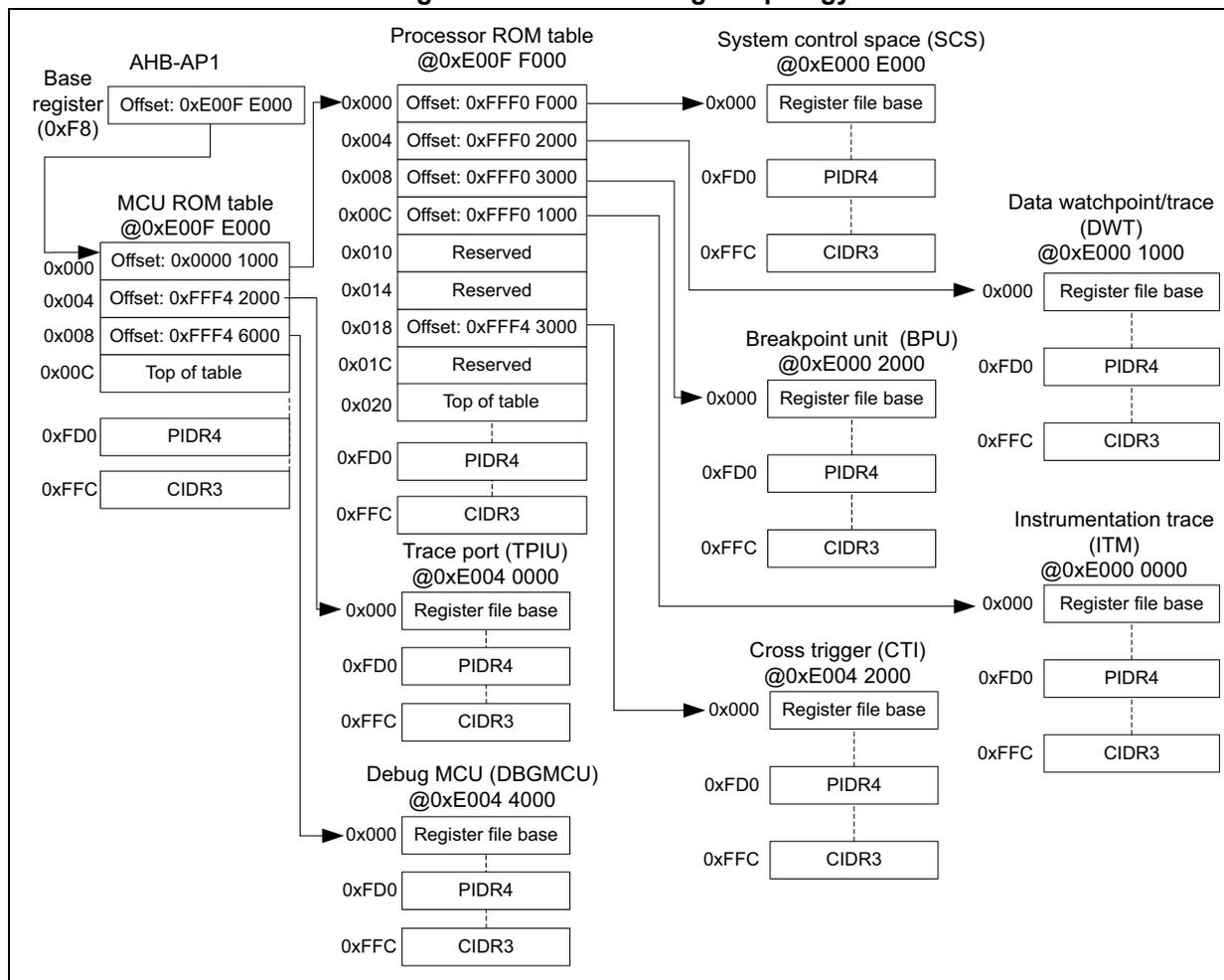
The diagram illustrates the CoreSight topology for debug components in the CPU sub-system. It shows the following components and their connections:
- AHB-AP1 : Base register (0xF8) at offset 0xE00F E000. It contains a MCU ROM table at 0xE00F E000 with entries at 0x000 (0x00000 1000), 0x004 (0xFFF4 2000), 0x008 (0xFFF4 6000), and 0x00C (Top of table). It also includes PIDR4 at 0xFD0 and CIDR3 at 0xFFC.
- Processor ROM table : Located at 0xE00F F000. It contains entries at 0x000 (0xFFF0 F000), 0x004 (0xFFF0 2000), 0x008 (0xFFF0 3000), 0x00C (0xFFF0 1000), 0x010 (Reserved), 0x014 (Reserved), 0x018 (0xFFF4 3000), 0x01C (Reserved), and 0x020 (Top of table). It also includes PIDR4 at 0xFD0 and CIDR3 at 0xFFC.
- System control space (SCS) : Located at 0xE000 E000. It contains a Register file base at 0x000, PIDR4 at 0xFD0, and CIDR3 at 0xFFC.
- Data watchpoint/trace (DWT) : Located at 0xE000 1000. It contains a Register file base at 0x000, PIDR4 at 0xFD0, and CIDR3 at 0xFFC.
- Breakpoint unit (BPU) : Located at 0xE000 2000. It contains a Register file base at 0x000, PIDR4 at 0xFD0, and CIDR3 at 0xFFC.
- Instrumentation trace (ITM) : Located at 0xE000 0000. It contains a Register file base at 0x000, PIDR4 at 0xFD0, and CIDR3 at 0xFFC.
- Cross trigger (CTI) : Located at 0xE004 2000. It contains a Register file base at 0x000, PIDR4 at 0xFD0, and CIDR3 at 0xFFC.
- Debug MCU (DBGMCU) : Located at 0xE004 4000. It contains a Register file base at 0x000, PIDR4 at 0xFD0, and CIDR3 at 0xFFC.
- Trace port (TPIU) : Located at 0xE004 0000. It contains a Register file base at 0x000, PIDR4 at 0xFD0, and CIDR3 at 0xFFC.
43.6.2 MCU and processor ROM memory type register (ROM_MEMTYPER)
Address offset: 0xFCC
Reset value: 0x0000 0001
| 31 | 30 | 29 | 28 | 27 | 26 | 25 | 24 | 23 | 22 | 21 | 20 | 19 | 18 | 17 | 16 |
|---|---|---|---|---|---|---|---|---|---|---|---|---|---|---|---|
| Res. | Res. | Res. | Res. | Res. | Res. | Res. | Res. | Res. | Res. | Res. | Res. | Res. | Res. | Res. | Res. |
| 15 | 14 | 13 | 12 | 11 | 10 | 9 | 8 | 7 | 6 | 5 | 4 | 3 | 2 | 1 | 0 |
| Res. | Res. | Res. | Res. | Res. | Res. | Res. | Res. | Res. | Res. | Res. | Res. | Res. | Res. | Res. | SYSEMEN |
| r |
Bits 31:1 Reserved, must be kept at reset value.
Bit 0
SYSTEM
: System memory
1: System memory present on this bus
43.6.3 MCU and processor ROM CoreSight peripheral identity register 4 (ROM_PIDR4)
Address offset: 0xFD0
Reset value: 0x0000 0000 (MCU ROM)
Reset value: 0x0000 0004 (processor ROM)
| 31 | 30 | 29 | 28 | 27 | 26 | 25 | 24 | 23 | 22 | 21 | 20 | 19 | 18 | 17 | 16 |
|---|---|---|---|---|---|---|---|---|---|---|---|---|---|---|---|
| Res. | Res. | Res. | Res. | Res. | Res. | Res. | Res. | Res. | Res. | Res. | Res. | Res. | Res. | Res. | Res. |
| 15 | 14 | 13 | 12 | 11 | 10 | 9 | 8 | 7 | 6 | 5 | 4 | 3 | 2 | 1 | 0 |
| Res. | Res. | Res. | Res. | Res. | Res. | Res. | Res. | F4KCOUNT[3:0] | JEP106CON[3:0] | ||||||
| r | r | r | r | r | r | r | r | ||||||||
Bits 31:8 Reserved, must be kept at reset value.
Bits 7:4
F4KCOUNT[3:0]
: Register file size
0x0: Register file occupies a single 4-Kbyte region.
Bits 3:0
JEP106CON[3:0]
: JEP106 continuation code
MCU ROM:
0x0: STMicroelectronics JEDEC continuation code
Processor ROM:
0x4: Arm® JEDEC continuation code
43.6.4 MCU and processor ROM CoreSight peripheral identity register 0 (ROM_PIDR0)
Address offset: 0xFE0
Reset value: 0x0000 0092 (MCU ROM)
Reset value: 0x0000 00C9 (processor ROM)
| 31 | 30 | 29 | 28 | 27 | 26 | 25 | 24 | 23 | 22 | 21 | 20 | 19 | 18 | 17 | 16 |
|---|---|---|---|---|---|---|---|---|---|---|---|---|---|---|---|
| Res. | Res. | Res. | Res. | Res. | Res. | Res. | Res. | Res. | Res. | Res. | Res. | Res. | Res. | Res. | Res. |
| 15 | 14 | 13 | 12 | 11 | 10 | 9 | 8 | 7 | 6 | 5 | 4 | 3 | 2 | 1 | 0 |
| Res. | Res. | Res. | Res. | Res. | Res. | Res. | Res. | PARTNUM[7:0] | |||||||
| r | r | r | r | r | r | r | r | ||||||||
Bits 31:8 Reserved, must be kept at reset value.
Bits 7:0 PARTNUM[7:0] : Part number bits [7:0]
MCU ROM:
0x92: STM32WBA5xxx
processor ROM:
0xC9: Cortex-M33
43.6.5 MCU and processor ROM CoreSight peripheral identity register 1 (ROM_PIDR1)
Address offset: 0xFE4
Reset value: 0x0000 0004 (MCU ROM)
Reset value: 0x0000 00B4 (processor ROM)
| 31 | 30 | 29 | 28 | 27 | 26 | 25 | 24 | 23 | 22 | 21 | 20 | 19 | 18 | 17 | 16 |
|---|---|---|---|---|---|---|---|---|---|---|---|---|---|---|---|
| Res. | Res. | Res. | Res. | Res. | Res. | Res. | Res. | Res. | Res. | Res. | Res. | Res. | Res. | Res. | Res. |
| 15 | 14 | 13 | 12 | 11 | 10 | 9 | 8 | 7 | 6 | 5 | 4 | 3 | 2 | 1 | 0 |
| Res. | Res. | Res. | Res. | Res. | Res. | Res. | Res. | JEP106ID[3:0] | PARTNUM[11:8] | ||||||
| r | r | r | r | r | r | r | r | ||||||||
Bits 31:8 Reserved, must be kept at reset value.
Bits 7:4 JEP106ID[3:0] : JEP106 identity code bits [3:0]
0x0: MCU ROM: STMicroelectronics JEDEC code
0xB: processor ROM: Arm® JEDEC code
Bits 3:0 PARTNUM[11:8] : Part number bits [11:8]
0x4: MCU ROM: STM32WBA5xxx
0x4: processor ROM: Cortex-M33
43.6.6 MCU and processor ROM CoreSight peripheral identity register 2 (ROM_PIDR2)
Address offset: 0xFE8
Reset value: 0x0000 000A (MCU ROM)
Reset value: 0x0000 000B (processor ROM)
| 31 | 30 | 29 | 28 | 27 | 26 | 25 | 24 | 23 | 22 | 21 | 20 | 19 | 18 | 17 | 16 |
|---|---|---|---|---|---|---|---|---|---|---|---|---|---|---|---|
| Res. | Res. | Res. | Res. | Res. | Res. | Res. | Res. | Res. | Res. | Res. | Res. | Res. | Res. | Res. | Res. |
| 15 | 14 | 13 | 12 | 11 | 10 | 9 | 8 | 7 | 6 | 5 | 4 | 3 | 2 | 1 | 0 |
| Res. | Res. | Res. | Res. | Res. | Res. | Res. | Res. | REVISION[3:0] | JEDEC | JEP106ID[6:4] | |||||
| r | r | r | r | r | r | r | r | ||||||||
Bits 31:8 Reserved, must be kept at reset value.
Bits 7:4 REVISION[3:0] : Component revision number
0x0: rev r0p0
Bit 3 JEDEC : JEDEC assigned value
1: Designer ID specified by JEDEC
Bits 2:0 JEP106ID[6:4] : JEP106 identity code bits [6:4]
MCU ROM:
0x2: STMicroelectronics JEDEC code
processor ROM:
0x3: Arm ® JEDEC code
43.6.7 MCU and processor ROM CoreSight peripheral identity register 3 (ROM_PIDR3)
Address offset: 0xFEC
Reset value: 0x0000 0000
| 31 | 30 | 29 | 28 | 27 | 26 | 25 | 24 | 23 | 22 | 21 | 20 | 19 | 18 | 17 | 16 |
|---|---|---|---|---|---|---|---|---|---|---|---|---|---|---|---|
| Res. | Res. | Res. | Res. | Res. | Res. | Res. | Res. | Res. | Res. | Res. | Res. | Res. | Res. | Res. | Res. |
| 15 | 14 | 13 | 12 | 11 | 10 | 9 | 8 | 7 | 6 | 5 | 4 | 3 | 2 | 1 | 0 |
| Res. | Res. | Res. | Res. | Res. | Res. | Res. | Res. | REVAND[3:0] | CMOD[3:0] | ||||||
| r | r | r | r | r | r | r | r | ||||||||
Bits 31:8 Reserved, must be kept at reset value.
Bits 7:4 REVAND[3:0] : Metal fix version
0x0: No metal fix
Bits 3:0 CMOD[3:0] : Customer modified
0x0: No customer modifications
43.6.8 MCU and processor ROM CoreSight component identity register 0 (ROM_CIDR0)
Address offset: 0xFF0
Reset value: 0x0000 000D
| 31 | 30 | 29 | 28 | 27 | 26 | 25 | 24 | 23 | 22 | 21 | 20 | 19 | 18 | 17 | 16 |
|---|---|---|---|---|---|---|---|---|---|---|---|---|---|---|---|
| Res. | Res. | Res. | Res. | Res. | Res. | Res. | Res. | Res. | Res. | Res. | Res. | Res. | Res. | Res. | Res. |
| 15 | 14 | 13 | 12 | 11 | 10 | 9 | 8 | 7 | 6 | 5 | 4 | 3 | 2 | 1 | 0 |
| Res. | Res. | Res. | Res. | Res. | Res. | Res. | Res. | PREAMBLE[7:0] | |||||||
| r | r | r | r | r | r | r | r | ||||||||
Bits 31:8 Reserved, must be kept at reset value.
Bits 7:0 PREAMBLE[7:0] : Component ID bits [7:0]
0x0D: Common ID value
43.6.9 MCU and processor ROM CoreSight peripheral identity register 1 (ROM_CIDR1)
Address offset: 0xFF4
Reset value: 0x0000 0010
| 31 | 30 | 29 | 28 | 27 | 26 | 25 | 24 | 23 | 22 | 21 | 20 | 19 | 18 | 17 | 16 |
|---|---|---|---|---|---|---|---|---|---|---|---|---|---|---|---|
| Res. | Res. | Res. | Res. | Res. | Res. | Res. | Res. | Res. | Res. | Res. | Res. | Res. | Res. | Res. | Res. |
| 15 | 14 | 13 | 12 | 11 | 10 | 9 | 8 | 7 | 6 | 5 | 4 | 3 | 2 | 1 | 0 |
| Res. | Res. | Res. | Res. | Res. | Res. | Res. | Res. | CLASS[3:0] | PREAMBLE[11:8] | ||||||
| r | r | r | r | r | r | r | r | ||||||||
Bits 31:8 Reserved, must be kept at reset value.
Bits 7:4 CLASS[3:0] : Component ID bits [15:12] - component class
0x1: ROM table component
Bits 3:0 PREAMBLE[11:8] : Component ID bits [11:8]
0x0: Common ID value
43.6.10 MCU and processor ROM CoreSight component identity register 2 (ROM_CIDR2)
Address offset: 0xFF8
Reset value: 0x0000 0005
| 31 | 30 | 29 | 28 | 27 | 26 | 25 | 24 | 23 | 22 | 21 | 20 | 19 | 18 | 17 | 16 |
|---|---|---|---|---|---|---|---|---|---|---|---|---|---|---|---|
| Res. | Res. | Res. | Res. | Res. | Res. | Res. | Res. | Res. | Res. | Res. | Res. | Res. | Res. | Res. | Res. |
| 15 | 14 | 13 | 12 | 11 | 10 | 9 | 8 | 7 | 6 | 5 | 4 | 3 | 2 | 1 | 0 |
| Res. | Res. | Res. | Res. | Res. | Res. | Res. | Res. | PREAMBLE[19:12] | |||||||
| r | r | r | r | r | r | r | r | ||||||||
Bits 31:8 Reserved, must be kept at reset value.
Bits 7:0 PREAMBLE[19:12] : Component ID bits [23:16]
0x05: Common ID value
43.6.11 MCU and processor ROM CoreSight component identity register 3 (ROM_CIDR3)Address offset: 0xFFC
Reset value: 0x0000 00B1
| 31 | 30 | 29 | 28 | 27 | 26 | 25 | 24 | 23 | 22 | 21 | 20 | 19 | 18 | 17 | 16 |
|---|---|---|---|---|---|---|---|---|---|---|---|---|---|---|---|
| Res. | Res. | Res. | Res. | Res. | Res. | Res. | Res. | Res. | Res. | Res. | Res. | Res. | Res. | Res. | Res. |
| 15 | 14 | 13 | 12 | 11 | 10 | 9 | 8 | 7 | 6 | 5 | 4 | 3 | 2 | 1 | 0 |
| Res. | Res. | Res. | Res. | Res. | Res. | Res. | Res. | PREAMBLE[27:20] | |||||||
| r | r | r | r | r | r | r | r | ||||||||
Bits 31:8 Reserved, must be kept at reset value.
Bits 7:0 PREAMBLE[27:20] : Component ID bits [31:24]0xB1: Common ID value
43.6.12 MCU and processor ROM tables register map and reset values
Table 429. ROM table register map and reset values
| Offset | Register name | 31 | 30 | 29 | 28 | 27 | 26 | 25 | 24 | 23 | 22 | 21 | 20 | 19 | 18 | 17 | 16 | 15 | 14 | 13 | 12 | 11 | 10 | 9 | 8 | 7 | 6 | 5 | 4 | 3 | 2 | 1 | 0 | |
|---|---|---|---|---|---|---|---|---|---|---|---|---|---|---|---|---|---|---|---|---|---|---|---|---|---|---|---|---|---|---|---|---|---|---|
| 0xFCC | ROM_MEMTYPER | Res. | Res. | Res. | Res. | Res. | Res. | Res. | Res. | Res. | Res. | Res. | Res. | Res. | Res. | Res. | Res. | Res. | Res. | Res. | Res. | Res. | Res. | Res. | Res. | Res. | Res. | Res. | Res. | Res. | Res. | Res. | Res. | SYSTEMEM |
| Reset value | 1 | |||||||||||||||||||||||||||||||||
| 0xFD0 | ROM_PIDR4 | Res. | Res. | Res. | Res. | Res. | Res. | Res. | Res. | Res. | Res. | Res. | Res. | Res. | Res. | Res. | Res. | Res. | Res. | Res. | Res. | Res. | Res. | Res. | Res. | F4KCOUNT [3:0] | JEP106CON [3:0] | |||||||
| MCU Reset value | 0 | 0 | 0 | 0 | 0 | 0 | 0 | 0 | ||||||||||||||||||||||||||
| processor Reset value | 0 | 0 | 0 | 0 | 0 | 1 | 0 | 0 | ||||||||||||||||||||||||||
| 0xFD4-0xFDC | Reserved | Reserved. | ||||||||||||||||||||||||||||||||
| 0xFE0 | ROM_PIDR0 | Res. | Res. | Res. | Res. | Res. | Res. | Res. | Res. | Res. | Res. | Res. | Res. | Res. | Res. | Res. | Res. | Res. | Res. | Res. | Res. | Res. | Res. | Res. | Res. | PARTNUM[7:0] | ||||||||
| MCU Reset value | 1 | 0 | 0 | 1 | 0 | 0 | 1 | 0 | ||||||||||||||||||||||||||
| processor Reset value | 1 | 1 | 0 | 0 | 1 | 0 | 0 | 1 | ||||||||||||||||||||||||||
| 0xFE4 | ROM_PIDR1 | Res. | Res. | Res. | Res. | Res. | Res. | Res. | Res. | Res. | Res. | Res. | Res. | Res. | Res. | Res. | Res. | Res. | Res. | Res. | Res. | Res. | Res. | Res. | Res. | JEP106ID [3:0] | PARTNUM [11:8] | |||||||
| MCU Reset value | 0 | 0 | 0 | 0 | 0 | 0 | 1 | 0 | ||||||||||||||||||||||||||
| processor Reset value | 1 | 0 | 1 | 1 | 0 | 1 | 0 | 0 | ||||||||||||||||||||||||||
| 0xFE8 | ROM_PIDR2 | Res. | Res. | Res. | Res. | Res. | Res. | Res. | Res. | Res. | Res. | Res. | Res. | Res. | Res. | Res. | Res. | Res. | Res. | Res. | Res. | Res. | Res. | Res. | Res. | REVISION [3:0] | JEDEC | JEP106ID [6:4] | ||||||
| MCU Reset value | 0 | 0 | 0 | 0 | 0 | 1 | 0 | |||||||||||||||||||||||||||
| processor Reset value | 0 | 0 | 0 | 0 | 0 | 1 | 1 | |||||||||||||||||||||||||||
| 0xFEC | ROM_PIDR3 | Res. | Res. | Res. | Res. | Res. | Res. | Res. | Res. | Res. | Res. | Res. | Res. | Res. | Res. | Res. | Res. | Res. | Res. | Res. | Res. | Res. | Res. | Res. | Res. | REVAND[3:0] | CMOD[3:0] | |||||||
| Reset value | 0 | 0 | 0 | 0 | 0 | 0 | 0 | 0 | ||||||||||||||||||||||||||
| 0xFF0 | ROM_CIDR0 | Res. | Res. | Res. | Res. | Res. | Res. | Res. | Res. | Res. | Res. | Res. | Res. | Res. | Res. | Res. | Res. | Res. | Res. | Res. | Res. | Res. | Res. | Res. | Res. | PREAMBLE[7:0] | ||||||||
| Reset value | 0 | 0 | 0 | 0 | 0 | 1 | 1 | 0 | ||||||||||||||||||||||||||
| 0xFF4 | ROM_CIDR1 | Res. | Res. | Res. | Res. | Res. | Res. | Res. | Res. | Res. | Res. | Res. | Res. | Res. | Res. | Res. | Res. | Res. | Res. | Res. | Res. | Res. | Res. | Res. | Res. | CLASS[3:0] | PREAMBLE [11:8] | |||||||
| Reset value | 0 | 0 | 0 | 1 | 0 | 0 | 0 | 0 | ||||||||||||||||||||||||||
| 0xFF8 | ROM_CIDR2 | Res. | Res. | Res. | Res. | Res. | Res. | Res. | Res. | Res. | Res. | Res. | Res. | Res. | Res. | Res. | Res. | Res. | Res. | Res. | Res. | Res. | Res. | Res. | Res. | PREAMBLE[19:12] | ||||||||
| Reset value | 0 | 0 | 0 | 0 | 0 | 0 | 1 | 0 | ||||||||||||||||||||||||||
| 0xFFC | ROM_CIDR3 | Res. | Res. | Res. | Res. | Res. | Res. | Res. | Res. | Res. | Res. | Res. | Res. | Res. | Res. | Res. | Res. | Res. | Res. | Res. | Res. | Res. | Res. | Res. | Res. | PREAMBLE[27:20] | ||||||||
| Reset value | 1 | 0 | 1 | 1 | 0 | 0 | 0 | 1 | ||||||||||||||||||||||||||
43.7 Data watchpoint and trace unit (DWT)
The DWT provides four comparators that can be used as one of the following function:
- • watchpoint
- • PC sampling trigger
- • data address sampling trigger
- • data comparator (comparator 1 only)
- • clock cycle counter comparator (comparator 0 only)
It also contains counters for:
- • clock cycles
- • folded instructions
- • load store unit (LSU) operations
- • sleep cycles
- • number of cycles per instruction
- • interrupt overhead
A DWT comparator compares the value held in its DWT_COMPxR registers with one of the following:
- • a data address
- • an instruction address
- • a data value
- • the cycle count value, for comparator 0 only.
For address matching, the comparator can use a mask, so it matches a range of addresses.
On a successful match, the comparator generates one of the following:
- • one or more DWT data trace packets, containing one or more of:
- – the address of the instruction that caused a data access
- – an address offset, bits[15:0] of the data access address
- – the matched data value
- • a watchpoint debug event, on either the PC value or the accessed data address
- • a CMPMATCH[N] event that signals the match outside the DWT unit
A watchpoint debug event either generates a DebugMonitor exception or causes the processor to halt execution and enter Debug state.
For more details on how to use the DWT, refer to the Armv8-M Architecture Reference Manual [4].
43.7.1 DWT control register (DWT_CTRLR)
Address offset: 0x000
Reset value: 0x4000 0000
| 31 | 30 | 29 | 28 | 27 | 26 | 25 | 24 | 23 | 22 | 21 | 20 | 19 | 18 | 17 | 16 |
|---|---|---|---|---|---|---|---|---|---|---|---|---|---|---|---|
| NUMCOMP[3:0] | NOTR CPKT | NOEXT TRIG | NOCYC CNT | NOPRF CNT | CYC DISS | CYCEV TENA | FOLDE VTENA | LSUEV TENA | SLEEPEVT ENA | EXCEVT ENA | CPIEV TENA | EXCTRC ENA | |||
| r | r | r | r | r | r | r | r | rw | rw | rw | rw | rw | rw | rw | rw |
| 15 | 14 | 13 | 12 | 11 | 10 | 9 | 8 | 7 | 6 | 5 | 4 | 3 | 2 | 1 | 0 |
| Res. | Res. | Res. | PCSAMPL ENA | SYNCTAP[1:0] | CYCTAP | POSTINIT[3:0] | POSTPRESET[3:0] | CYCCNT ENA | |||||||
| rw | rw | rw | rw | rw | rw | rw | rw | rw | rw | rw | rw | rw | |||
Bits 31:28 NUMCOMP[3:0] : Number of comparators implemented (read only)
0x4: Four comparators
Bit 27 NOTRCPKT : Trace sampling and exception tracing support (read only)
0: Supported
Bit 26 NOEXTTRIG : External match signal, CMPMATCH support (read only)
0: Supported
Bit 25 NOCYCCNT : Cycle counter support (read only)
0: Supported
Bit 24 NOPRFCNT : Profiling counter support (read only)
0: Supported
Bit 23 CYCDISS : Cycle counter disable secure
Controls whether the cycle counter is disabled in secure mode
0: No effect
1: Disabled incrementing the cycle counter when the processor is in secure mode
Bit 22 CYCEVTENA : Enable for POSTCNT underflow event counter packet generation
0: Disabled
1: Enabled
Bit 21 FOLDEVTENA : Enable for folded instruction counter overflow event generation
0: Disabled
1: Enabled
Bit 20 LSUEVTENA : Enable for LSU counter overflow event generation
0: Disabled
1: Enabled
Bit 19 SLEEPEVTENA : Enable for sleep counter overflow event generation
0: Disabled
1: Enabled
Bit 18 EXCEVTENA : Enable for exception overhead counter overflow event generation
0: Disabled
1: Enabled
Bit 17 CPIEVTENA : Enable for CPI counter overflow event generation
0: Disabled
1: Enabled
Bit 16 EXCTRCENA : Enable for exception trace generation
- 0: Disabled
- 1: Enabled
Bits 15:13 Reserved, must be kept at reset value.
Bit 12 PCSAMPLENA : Enable for POSTCNT counter used as a timer for periodic PC sample packet generation
- 0: Disabled
- 1: Enabled
Bits 11:10 SYNCTAP[1:0] : synchronization packet counter tap
Selects the position of the synchronization packet counter tap on the CYCCNT counter. This determines the synchronization packet rate.
- 00: Disabled. No synchronization packets
- 01: Tap at CYCCNT[24]
- 10: Tap at CYCCNT[26]
- 11: Tap at CYCCNT[28]
Bit 9 CYCTAP : Selects the position of the POSTCNT tap on the CYCCNT counter.
- 0: Tap at CYCCNT[6]
- 1: Tap at CYCCNT[10]
Bits 8:5 POSTINIT[3:0] : initial value of the POSTCNT counter
Writes to this field are ignored if POSTCNT counter is enabled (CYCEVTENA or PCSAMPLENA must be reset prior to writing POSTINIT).
Bits 4:1 POSTPRESET[3:0] : Reloads value of the POSTCNT counter.
Bit 0 CYCCNTENA : Enable for CYCCNT counter
- 0: Disabled
- 1: Enabled
43.7.2 DWT cycle count register (DWT_CYCCNTR)
Address offset: 0x004
Reset value: 0x0000 0000
| 31 | 30 | 29 | 28 | 27 | 26 | 25 | 24 | 23 | 22 | 21 | 20 | 19 | 18 | 17 | 16 |
| CYCCNT[31:16] | |||||||||||||||
| r | r | r | r | r | r | r | r | r | r | r | r | r | r | r | r |
| 15 | 14 | 13 | 12 | 11 | 10 | 9 | 8 | 7 | 6 | 5 | 4 | 3 | 2 | 1 | 0 |
| CYCCNT[15:0] | |||||||||||||||
| r | r | r | r | r | r | r | r | r | r | r | r | r | r | r | r |
Bits 31:0 CYCCNT[31:0] : processor clock cycle counter
43.7.3 DWT CPI count register (DWT_CPICNTR)
Address offset: 0x008
Reset value: 0x0000 0000
| 31 | 30 | 29 | 28 | 27 | 26 | 25 | 24 | 23 | 22 | 21 | 20 | 19 | 18 | 17 | 16 |
|---|---|---|---|---|---|---|---|---|---|---|---|---|---|---|---|
| Res. | Res. | Res. | Res. | Res. | Res. | Res. | Res. | Res. | Res. | Res. | Res. | Res. | Res. | Res. | Res. |
| 15 | 14 | 13 | 12 | 11 | 10 | 9 | 8 | 7 | 6 | 5 | 4 | 3 | 2 | 1 | 0 |
| Res. | Res. | Res. | Res. | Res. | Res. | Res. | Res. | CPICNT[7:0] | |||||||
| rw | rw | rw | rw | rw | rw | rw | rw | ||||||||
Bits 31:8 Reserved, must be kept at reset value.
Bits 7:0 CPICNT[7:0] : CPI counter
Counts additional cycles required to execute multi-cycle instructions (except those recorded by DWT_LSUCNTR) and counts any instruction fetch stalls.
43.7.4 DWT exception count register (DWT_EXCCNTR)
Address offset: 0x00C
Reset value: 0x0000 0000
| 31 | 30 | 29 | 28 | 27 | 26 | 25 | 24 | 23 | 22 | 21 | 20 | 19 | 18 | 17 | 16 |
|---|---|---|---|---|---|---|---|---|---|---|---|---|---|---|---|
| Res. | Res. | Res. | Res. | Res. | Res. | Res. | Res. | Res. | Res. | Res. | Res. | Res. | Res. | Res. | Res. |
| 15 | 14 | 13 | 12 | 11 | 10 | 9 | 8 | 7 | 6 | 5 | 4 | 3 | 2 | 1 | 0 |
| Res. | Res. | Res. | Res. | Res. | Res. | Res. | Res. | EXCCNT[7:0] | |||||||
| rw | rw | rw | rw | rw | rw | rw | rw | ||||||||
Bits 31:8 Reserved, must be kept at reset value.
Bits 7:0 EXCCNT[7:0] : exception overhead cycle counter
Counts the number of cycles spent in exception processing.
43.7.5 DWT sleep count register (DWT_SLPCNTR)
Address offset: 0x010
Reset value: 0x0000 0000
| 31 | 30 | 29 | 28 | 27 | 26 | 25 | 24 | 23 | 22 | 21 | 20 | 19 | 18 | 17 | 16 |
|---|---|---|---|---|---|---|---|---|---|---|---|---|---|---|---|
| Res. | Res. | Res. | Res. | Res. | Res. | Res. | Res. | Res. | Res. | Res. | Res. | Res. | Res. | Res. | Res. |
| 15 | 14 | 13 | 12 | 11 | 10 | 9 | 8 | 7 | 6 | 5 | 4 | 3 | 2 | 1 | 0 |
| Res. | Res. | Res. | Res. | Res. | Res. | Res. | Res. | SLEEPCNT[7:0] | |||||||
| rw | rw | rw | rw | rw | rw | rw | rw | ||||||||
Bits 31:8 Reserved, must be kept at reset value.
Bits 7:0 SLEEPCNT[7:0] : sleep cycle counter
Counts the number of cycles spent in sleep mode (WFI, WFE, sleep-on-exit).
43.7.6 DWT LSU count register (DWT_LSUCNTR)
Address offset: 0x014
Reset value: 0x0000 0000
| 31 | 30 | 29 | 28 | 27 | 26 | 25 | 24 | 23 | 22 | 21 | 20 | 19 | 18 | 17 | 16 |
|---|---|---|---|---|---|---|---|---|---|---|---|---|---|---|---|
| Res. | Res. | Res. | Res. | Res. | Res. | Res. | Res. | Res. | Res. | Res. | Res. | Res. | Res. | Res. | Res. |
| 15 | 14 | 13 | 12 | 11 | 10 | 9 | 8 | 7 | 6 | 5 | 4 | 3 | 2 | 1 | 0 |
| Res. | Res. | Res. | Res. | Res. | Res. | Res. | Res. | ||||||||
| rw | rw | rw | rw | rw | rw | rw | rw |
Bits 31:8 Reserved, must be kept at reset value.
Bits 7:0 LSUCNT[7:0] : load store counter
Counts additional cycles required to execute load and store instructions.
43.7.7 DWT fold count register (DWT_FOLDCNTR)
Address offset: 0x018
Reset value: 0x0000 0000
| 31 | 30 | 29 | 28 | 27 | 26 | 25 | 24 | 23 | 22 | 21 | 20 | 19 | 18 | 17 | 16 |
|---|---|---|---|---|---|---|---|---|---|---|---|---|---|---|---|
| Res. | Res. | Res. | Res. | Res. | Res. | Res. | Res. | Res. | Res. | Res. | Res. | Res. | Res. | Res. | Res. |
| 15 | 14 | 13 | 12 | 11 | 10 | 9 | 8 | 7 | 6 | 5 | 4 | 3 | 2 | 1 | 0 |
| Res. | Res. | Res. | Res. | Res. | Res. | Res. | Res. | ||||||||
| rw | rw | rw | rw | rw | rw | rw | rw |
Bits 31:8 Reserved, must be kept at reset value.
Bits 7:0 FOLDCNT[7:0] : folded instruction counter
Increments on each instruction that takes 0 cycles.
43.7.8 DWT program counter sample register (DWT_PCSR)
Address offset: 0x01C
Reset value: 0x0000 0000
| 31 | 30 | 29 | 28 | 27 | 26 | 25 | 24 | 23 | 22 | 21 | 20 | 19 | 18 | 17 | 16 |
| EIASAMPLE[31:16] | |||||||||||||||
| r | r | r | r | r | r | r | r | r | r | r | r | r | r | r | r |
| 15 | 14 | 13 | 12 | 11 | 10 | 9 | 8 | 7 | 6 | 5 | 4 | 3 | 2 | 1 | 0 |
| EIASAMPLE[15:0] | |||||||||||||||
| r | r | r | r | r | r | r | r | r | r | r | r | r | r | r | r |
Bits 31:0
EIASAMPLE[31:0]
: executed Instruction Address sample value
Samples the current value of the program counter.
43.7.9 DWT comparator register x (DWT_COMPxR)
Address offset: 0x020 + 0x10 * x, (x = 0 to 3)
Reset value: 0x0000 0000
| 31 | 30 | 29 | 28 | 27 | 26 | 25 | 24 | 23 | 22 | 21 | 20 | 19 | 18 | 17 | 16 |
| COMP[31:16] | |||||||||||||||
| r | r | r | r | r | r | r | r | r | r | r | r | r | r | r | r |
| 15 | 14 | 13 | 12 | 11 | 10 | 9 | 8 | 7 | 6 | 5 | 4 | 3 | 2 | 1 | 0 |
| COMP[15:0] | |||||||||||||||
| r | r | r | r | r | r | r | r | r | r | r | r | r | r | r | r |
Bits 31:0 COMP[31:0] : reference value for comparison
43.7.10 DWT function register 0(DWT_FUNCTR0)
Address offset: 0x028
Reset value: 0x5800 0000
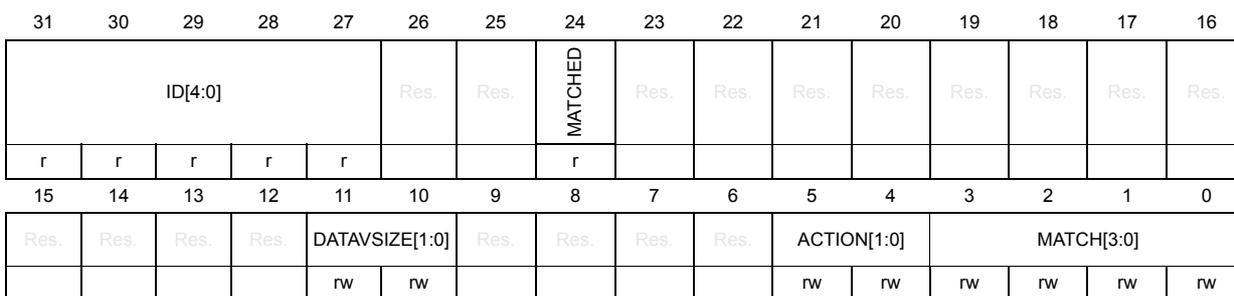
| 31 | 30 | 29 | 28 | 27 | 26 | 25 | 24 | 23 | 22 | 21 | 20 | 19 | 18 | 17 | 16 |
| ID[4:0] | Res. | Res. | MATCHED | Res. | Res. | Res. | Res. | Res. | Res. | Res. | Res. | ||||
| r | r | r | r | r | r | ||||||||||
| 15 | 14 | 13 | 12 | 11 | 10 | 9 | 8 | 7 | 6 | 5 | 4 | 3 | 2 | 1 | 0 |
| Res. | Res. | Res. | Res. | DATAVSIZE[1:0] | Res. | Res. | Res. | Res. | ACTION[1:0] | MATCH[3:0] | |||||
| rw | rw | rw | rw | rw | rw | rw | rw | ||||||||
Bits 31:27 ID[4:0] : capability identification
Identifies the capability for match for comparator 0.
0b01011: Cycle Counter, Instruction Address, Data Address and Data Address With Value
Bits 26:25 Reserved, must be kept at reset value.
Bit 24 MATCHED : comparator match
Indicates if a comparator match has occurred since the register was last read.
0: No match
1: A match occurred
Bits 23:12 Reserved, must be kept at reset value.
Bits 11:10 DATAVSIZE[1:0] : Data value size
Defines the size of the object being watched for by Data Value and Data Address comparators.
0x0: 1 byte
0x1: 2 bytes
0x2: 4 bytes
0x3: reserved
Bits 9:6 Reserved, must be kept at reset value.
Bits 5:4 ACTION[1:0] : Action on match
0x0: trigger only
0x1: generate debug event
0x2: For a Cycle Counter, Instruction Address, Data Address, Data Value or Linked Data Value comparator, generate a Data Trace Match packet. For a Data Address With Value comparator, generate a Data Trace Data Value packet.
0x3: For a Data Address Limit comparator, generate a Data Trace Data Address packet. For a Cycle Counter, Instruction Address Limit, or Data Address comparator, generate a Data Trace PC Value packet. For a Data Address With Value comparator, generate both a Data Trace PC Value packet and a Data Trace Data Value packet.
Bits 3:0 MATCH[3:0] : Match type
Controls the type of match generated by comparator 0.
For possible values of this field, refer to [4].
DWT function register 1 (DWT_FUNCTR1)
Address offset: 0x038
Reset value: 0xD000 0000
| 31 | 30 | 29 | 28 | 27 | 26 | 25 | 24 | 23 | 22 | 21 | 20 | 19 | 18 | 17 | 16 |
|---|---|---|---|---|---|---|---|---|---|---|---|---|---|---|---|
| ID[4:0] | Res. | Res. | MATCHED | Res. | Res. | Res. | Res. | Res. | Res. | Res. | Res. | ||||
| r | r | r | r | r | r | ||||||||||
| 15 | 14 | 13 | 12 | 11 | 10 | 9 | 8 | 7 | 6 | 5 | 4 | 3 | 2 | 1 | 0 |
| Res. | Res. | Res. | Res. | DATAVSIZE[1:0] | Res. | Res. | Res. | Res. | ACTION[1:0] | MATCH[3:0] | |||||
| rw | rw | rw | rw | rw | rw | rw | rw | ||||||||
Bits 31:27 ID[4:0] : capability identification
Identifies the capability for match for comparator 1.
0b11010: Instruction Address, Instruction Address Limit, Data Address, Data Address Limit, and Data Address With Value
Bits 26:25 Reserved, must be kept at reset value.
Bit 24 MATCHED : Comparator match
Indicates if a comparator match has occurred since the register was last read.
0: no match
1: a match occurred
Bits 23:12 Reserved, must be kept at reset value.
Bits 11:10 DATAVSIZE[1:0] : Data value size
Defines the size of the object being watched for by Data Value and Data Address comparators.
0x0: 1 byte
0x1: 2 bytes
0x2: 4 bytes
0x3: reserved
Bits 9:6 Reserved, must be kept at reset value.
Bits 5:4 ACTION[1:0] : Action on match
0x0: trigger only
0x1: generate debug event
0x2: For a Cycle Counter, Instruction Address, Data Address, Data Value or Linked Data Value comparator, generate a Data Trace Match packet. For a Data Address With Value comparator, generate a Data Trace Data Value packet.
0x3: For a Data Address Limit comparator, generate a Data Trace Data Address packet. For a Cycle Counter, Instruction Address Limit, or Data Address comparator, generate a Data Trace PC Value packet. For a Data Address With Value comparator, generate both a Data Trace PC Value packet and a Data Trace Data Value packet.
Bits 3:0 MATCH[3:0] : Match type
Controls the type of match generated by comparator 1.
For possible values of this field, refer to [4].
DWT function register 2 (DWT_FUNCTR2)
Address offset: 0x048
Reset value: 0x5000 0000
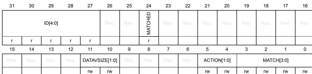
| 31 | 30 | 29 | 28 | 27 | 26 | 25 | 24 | 23 | 22 | 21 | 20 | 19 | 18 | 17 | 16 |
| ID[4:0] | Res. | Res. | MATCHED | Res. | Res. | Res. | Res. | Res. | Res. | Res. | Res. | ||||
| r | r | r | r | r | 1 | ||||||||||
| 15 | 14 | 13 | 12 | 11 | 10 | 9 | 8 | 7 | 6 | 5 | 4 | 3 | 2 | 1 | 0 |
| Res. | Res. | Res. | Res. | DATAVSIZE[1:0] | Res. | Res. | Res. | Res. | ACTION[1:0] | MATCH[3:0] | |||||
| rw | rw | rw | rw | rw | rw | rw | rw | ||||||||
Bits 31:27 ID[4:0] : capability identification
Identifies the capability for MATCH for comparator 2
0b01010: Instruction Address, Data Address, and Data Address With Value
Bits 26:25 Reserved, must be kept at reset value.
Bit 24 MATCHED : comparator match
Indicates if a comparator match has occurred since the register was last read.
0: no match
1: a match occurred
Bits 23:12 Reserved, must be kept at reset value.
Bits 11:10 DATAVSIZE[1:0] : Data value size:
Defines the size of the object being watched for by Data Value and Data Address comparators.
0x0: 1 byte
0x1: 2 bytes
0x2: 4 bytes
0x3: reserved
Bits 9:6 Reserved, must be kept at reset value.
Bits 5:4 ACTION[1:0] : Action on match
0x0: trigger only
0x1: Generate debug event
0x2: For a Cycle Counter, Instruction Address, Data Address, Data Value or Linked Data Value comparator, generate a Data Trace Match packet. For a Data Address With Value comparator, generate a Data Trace Data Value packet.
0x3: For a Data Address Limit comparator, generate a Data Trace Data Address packet. For a Cycle Counter, Instruction Address Limit, or Data Address comparator, generate a Data Trace PC Value packet. For a Data Address With Value comparator, generate both a Data Trace PC Value packet and a Data Trace Data Value packet.
Bits 3:0 MATCH[3:0] : Match type
Controls the type of match generated by comparator 2.
For possible values of this field, refer to [4].
DWT function register 3 (DWT_FUNCTR3)
Address offset: 0x058
Reset value: 0xF000 0000
| 31 | 30 | 29 | 28 | 27 | 26 | 25 | 24 | 23 | 22 | 21 | 20 | 19 | 18 | 17 | 16 |
|---|---|---|---|---|---|---|---|---|---|---|---|---|---|---|---|
| ID[4:0] | Res. | Res. | MATCHED | Res. | Res. | Res. | Res. | Res. | Res. | Res. | Res. | ||||
| r | r | r | r | r | 1 | ||||||||||
| 15 | 14 | 13 | 12 | 11 | 10 | 9 | 8 | 7 | 6 | 5 | 4 | 3 | 2 | 1 | 0 |
| Res. | Res. | Res. | Res. | DATAVSIZE[1:0] | Res. | Res. | Res. | Res. | ACTION[1:0] | MATCH[3:0] | |||||
| rw | rw | rw | rw | rw | rw | rw | rw | ||||||||
Bits 31:27 ID[4:0] : capability identification
Identifies the capability for MATCH for comparator 2.
0b11110: Instruction Address, Instruction Address Limit, Data Address, Data Address Limit, Data value, Linked Data Value, and Data Address With Value
Bits 26:25 Reserved, must be kept at reset value.
Bit 24 MATCHED : comparator match
Indicates if a comparator match has occurred since the register was last read.
0: no match
1: a match occurred
Bits 23:12 Reserved, must be kept at reset value.
Bits 11:10 DATAVSIZE[1:0] : Data value size
Defines the size of the object being watched for by Data Value and Data Address comparators.
0x0: 1 byte
0x1: 2 bytes
0x2: 4 bytes
0x3: reserved
Bits 9:6 Reserved, must be kept at reset value.
Bits 5:4 ACTION[1:0] : Action on match
0x0: trigger only
0x1: Generate debug event
0x2: For a Cycle Counter, Instruction Address, Data Address, Data Value or Linked Data Value comparator, generate a Data Trace Match packet. For a Data Address With Value comparator, generate a Data Trace Data Value packet.
0x3: For a Data Address Limit comparator, generate a Data Trace Data Address packet. For a Cycle Counter, Instruction Address Limit, or Data Address comparator, generate a Data Trace PC Value packet. For a Data Address With Value comparator, generate both a Data Trace PC Value packet and a Data Trace Data Value packet.
Bits 3:0 MATCH[3:0] : Match type
Controls the type of match generated by comparator 2.
For possible values of this field, refer to [4].
43.7.11 DWT device type architecture register (DWT_DEVARCHR)
Address offset: 0xFC8
Reset value: 0x4770 1A02
| 31 | 30 | 29 | 28 | 27 | 26 | 25 | 24 | 23 | 22 | 21 | 20 | 19 | 18 | 17 | 16 |
|---|---|---|---|---|---|---|---|---|---|---|---|---|---|---|---|
| ARCHITECT[10:0] | PRESENT | REVISION[3:0] | |||||||||||||
| r | r | r | r | r | r | r | r | r | r | r | r | r | r | r | r |
| 15 | 14 | 13 | 12 | 11 | 10 | 9 | 8 | 7 | 6 | 5 | 4 | 3 | 2 | 1 | 0 |
| ARCHVER[3:0] | ARCHPART[11:0] | ||||||||||||||
| r | r | r | r | r | r | r | r | r | r | r | r | r | r | r | r |
Bits 31:21 ARCHITECT[10:0] : Architect JEP106 code
0x23B: JEP106 continuation code 0x4, JEP106 ID code 0x3B Arm ® .
Bit 20 PRESENT : DWT_DEVARCH register present
0x1: Present.
Bits 19:16 REVISION[3:0] : Architecture revision
0x0: DWT architecture v2.0.
Bits 15:12
ARCHVER[3:0]
: Architecture version
0x1: DWT architecture v2.0.
Bits 11:0
ARCHPART[11:0]
: Architecture part
0xA02: DWT architecture
43.7.12 DWT device type register 4 (DWT_DEVTYPE)
Address offset: 0xFCC
Reset value: 0x0000 0000
| 31 | 30 | 29 | 28 | 27 | 26 | 25 | 24 | 23 | 22 | 21 | 20 | 19 | 18 | 17 | 16 |
|---|---|---|---|---|---|---|---|---|---|---|---|---|---|---|---|
| Res. | Res. | Res. | Res. | Res. | Res. | Res. | Res. | Res. | Res. | Res. | Res. | Res. | Res. | Res. | Res. |
| 15 | 14 | 13 | 12 | 11 | 10 | 9 | 8 | 7 | 6 | 5 | 4 | 3 | 2 | 1 | 0 |
| Res. | Res. | Res. | Res. | Res. | Res. | Res. | Res. | SUB[3:0] | MAJOR[3:0] | ||||||
| r | r | r | r | r | r | r | r | ||||||||
Bits 31:8 Reserved, must be kept at reset value.
Bits 7:4
SUB[3:0]
: Sub-type
0x0: Other
Bits 3:0
MAJOR[3:0]
: Major type
0x0: Miscellaneous
43.7.13 DWT CoreSight peripheral identity register 4 (DWT_PIDR4)
Address offset: 0xFD0
Reset value: 0x0000 0004
| 31 | 30 | 29 | 28 | 27 | 26 | 25 | 24 | 23 | 22 | 21 | 20 | 19 | 18 | 17 | 16 |
|---|---|---|---|---|---|---|---|---|---|---|---|---|---|---|---|
| Res. | Res. | Res. | Res. | Res. | Res. | Res. | Res. | Res. | Res. | Res. | Res. | Res. | Res. | Res. | Res. |
| 15 | 14 | 13 | 12 | 11 | 10 | 9 | 8 | 7 | 6 | 5 | 4 | 3 | 2 | 1 | 0 |
| Res. | Res. | Res. | Res. | Res. | Res. | Res. | Res. | F4KCOUNT[3:0] | JEP106CON[3:0] | ||||||
| r | r | r | r | r | r | r | r | ||||||||
Bits 31:8 Reserved, must be kept at reset value.
Bits 7:4
F4KCOUNT[3:0]
: Register file size
0x0: Register file occupies a single 4-Kbyte region.
Bits 3:0
JEP106CON[3:0]
: JEP106 continuation code
0x4: Arm® JEDEC code
43.7.14 DWT CoreSight peripheral identity register 0 (DWT_PIDR0)
Address offset: 0xFE0
Reset value: 0x0000 0021
| 31 | 30 | 29 | 28 | 27 | 26 | 25 | 24 | 23 | 22 | 21 | 20 | 19 | 18 | 17 | 16 |
|---|---|---|---|---|---|---|---|---|---|---|---|---|---|---|---|
| Res. | Res. | Res. | Res. | Res. | Res. | Res. | Res. | Res. | Res. | Res. | Res. | Res. | Res. | Res. | Res. |
| 15 | 14 | 13 | 12 | 11 | 10 | 9 | 8 | 7 | 6 | 5 | 4 | 3 | 2 | 1 | 0 |
| Res. | Res. | Res. | Res. | Res. | Res. | Res. | Res. | PARTNUM[7:0] | |||||||
| r | r | r | r | r | r | r | r | ||||||||
Bits 31:8 Reserved, must be kept at reset value.
Bits 7:0 PARTNUM[7:0] : Part number bits [7:0]
0x21: DWT part number
43.7.15 DWT CoreSight peripheral identity register 1 (DWT_PIDR1)
Address offset: 0xFE4
Reset value: 0x0000 00BD
| 31 | 30 | 29 | 28 | 27 | 26 | 25 | 24 | 23 | 22 | 21 | 20 | 19 | 18 | 17 | 16 |
|---|---|---|---|---|---|---|---|---|---|---|---|---|---|---|---|
| Res. | Res. | Res. | Res. | Res. | Res. | Res. | Res. | Res. | Res. | Res. | Res. | Res. | Res. | Res. | Res. |
| 15 | 14 | 13 | 12 | 11 | 10 | 9 | 8 | 7 | 6 | 5 | 4 | 3 | 2 | 1 | 0 |
| Res. | Res. | Res. | Res. | Res. | Res. | Res. | Res. | JEP106ID[3:0] | PARTNUM[11:8] | ||||||
| r | r | r | r | r | r | r | r | ||||||||
Bits 31:8 Reserved, must be kept at reset value.
Bits 7:4 JEP106ID[3:0] : JEP106 identity code bits [3:0]
0xB: Arm® JEDEC code
Bits 3:0 PARTNUM[11:8] : Part number bits [11:8]
0xD: DWT part number
43.7.16 DWT CoreSight peripheral identity register 2 (DWT_PIDR2)
Address offset: 0xFE8
Reset value: 0x0000 000B
| 31 | 30 | 29 | 28 | 27 | 26 | 25 | 24 | 23 | 22 | 21 | 20 | 19 | 18 | 17 | 16 |
|---|---|---|---|---|---|---|---|---|---|---|---|---|---|---|---|
| Res. | Res. | Res. | Res. | Res. | Res. | Res. | Res. | Res. | Res. | Res. | Res. | Res. | Res. | Res. | Res. |
| 15 | 14 | 13 | 12 | 11 | 10 | 9 | 8 | 7 | 6 | 5 | 4 | 3 | 2 | 1 | 0 |
| Res. | Res. | Res. | Res. | Res. | Res. | Res. | Res. | REVISION[3:0] | JEDEC | JEP106ID[6:4] | |||||
| r | r | r | r | r | r | r | r | ||||||||
Bits 31:8 Reserved, must be kept at reset value.
Bits 7:4 REVISION[3:0] : Component revision number
0x0: r0p0
Bit 3 JEDEC : JEDEC assigned value
0x1: designer ID specified by JEDEC
Bits 2:0 JEP106ID[6:4] : JEP106 identity code bits [6:4]
0x3: Arm® JEDEC code
43.7.17 DWT CoreSight peripheral identity register 3 (DWT_PIDR3)
Address offset: 0xFEC
Reset value: 0x0000 0000
| 31 | 30 | 29 | 28 | 27 | 26 | 25 | 24 | 23 | 22 | 21 | 20 | 19 | 18 | 17 | 16 |
|---|---|---|---|---|---|---|---|---|---|---|---|---|---|---|---|
| Res. | Res. | Res. | Res. | Res. | Res. | Res. | Res. | Res. | Res. | Res. | Res. | Res. | Res. | Res. | Res. |
| 15 | 14 | 13 | 12 | 11 | 10 | 9 | 8 | 7 | 6 | 5 | 4 | 3 | 2 | 1 | 0 |
| Res. | Res. | Res. | Res. | Res. | Res. | Res. | Res. | REVAND[3:0] | CMOD[3:0] | ||||||
| r | r | r | r | r | r | r | r | ||||||||
Bits 31:8 Reserved, must be kept at reset value.
Bits 7:4 REVAND[3:0] : Metal fix version
0x0: No metal fix
Bits 3:0 CMOD[3:0] : Customer modified
0x0: No customer modifications
43.7.18 DWT CoreSight component identity register 0 (DWT_CIDR0)
Address offset: 0xFF0
Reset value: 0x0000 000D
| 31 | 30 | 29 | 28 | 27 | 26 | 25 | 24 | 23 | 22 | 21 | 20 | 19 | 18 | 17 | 16 |
|---|---|---|---|---|---|---|---|---|---|---|---|---|---|---|---|
| Res. | Res. | Res. | Res. | Res. | Res. | Res. | Res. | Res. | Res. | Res. | Res. | Res. | Res. | Res. | Res. |
| 15 | 14 | 13 | 12 | 11 | 10 | 9 | 8 | 7 | 6 | 5 | 4 | 3 | 2 | 1 | 0 |
| Res. | Res. | Res. | Res. | Res. | Res. | Res. | Res. | PREAMBLE[7:0] | |||||||
| r | r | r | r | r | r | r | r | ||||||||
Bits 31:8 Reserved, must be kept at reset value.
Bits 7:0 PREAMBLE[7:0] : Component ID bits [7:0]
0x0D: Common ID value
43.7.19 DWT CoreSight peripheral identity register 1 (DWT_CIDR1)
Address offset: 0xFF4
Reset value: 0x0000 0090
| 31 | 30 | 29 | 28 | 27 | 26 | 25 | 24 | 23 | 22 | 21 | 20 | 19 | 18 | 17 | 16 |
|---|---|---|---|---|---|---|---|---|---|---|---|---|---|---|---|
| Res. | Res. | Res. | Res. | Res. | Res. | Res. | Res. | Res. | Res. | Res. | Res. | Res. | Res. | Res. | Res. |
| 15 | 14 | 13 | 12 | 11 | 10 | 9 | 8 | 7 | 6 | 5 | 4 | 3 | 2 | 1 | 0 |
| Res. | Res. | Res. | Res. | Res. | Res. | Res. | Res. | CLASS[3:0] | PREAMBLE[11:8] | ||||||
| r | r | r | r | r | r | r | r | ||||||||
Bits 31:8 Reserved, must be kept at reset value.
Bits 7:4 CLASS[3:0] : Component ID bits [15:12] - component class
0x9: Debug component
Bits 3:0 PREAMBLE[11:8] : Component ID bits [11:8]
0x0: Common ID value
43.7.20 DWT CoreSight component identity register 2 (DWT_CIDR2)
Address offset: 0xFF8
Reset value: 0x0000 0005
| 31 | 30 | 29 | 28 | 27 | 26 | 25 | 24 | 23 | 22 | 21 | 20 | 19 | 18 | 17 | 16 |
|---|---|---|---|---|---|---|---|---|---|---|---|---|---|---|---|
| Res. | Res. | Res. | Res. | Res. | Res. | Res. | Res. | Res. | Res. | Res. | Res. | Res. | Res. | Res. | Res. |
| 15 | 14 | 13 | 12 | 11 | 10 | 9 | 8 | 7 | 6 | 5 | 4 | 3 | 2 | 1 | 0 |
| Res. | Res. | Res. | Res. | Res. | Res. | Res. | Res. | PREAMBLE[19:12] | |||||||
| r | r | r | r | r | r | r | r | ||||||||
Bits 31:8 Reserved, must be kept at reset value.
Bits 7:0
PREAMBLE[19:12]
: Component ID bits [23:16]
0x05: Common ID value
43.7.21 DWT CoreSight component identity register 3 (DWT_CIDR3)
Address offset: 0xFFC
Reset value: 0x0000 00B1
| 31 | 30 | 29 | 28 | 27 | 26 | 25 | 24 | 23 | 22 | 21 | 20 | 19 | 18 | 17 | 16 |
|---|---|---|---|---|---|---|---|---|---|---|---|---|---|---|---|
| Res. | Res. | Res. | Res. | Res. | Res. | Res. | Res. | Res. | Res. | Res. | Res. | Res. | Res. | Res. | Res. |
| 15 | 14 | 13 | 12 | 11 | 10 | 9 | 8 | 7 | 6 | 5 | 4 | 3 | 2 | 1 | 0 |
| Res. | Res. | Res. | Res. | Res. | Res. | Res. | Res. | PREAMBLE[27:20] | |||||||
| r | r | r | r | r | r | r | r | ||||||||
Bits 31:8 Reserved, must be kept at reset value.
Bits 7:0
PREAMBLE[27:20]
: Component ID bits [31:24]
0xB1: Common ID value
43.7.22 DWT register map and reset values
Table 430. DWT register map and reset values
| Offset | Register name | 31 | 30 | 29 | 28 | 27 | 26 | 25 | 24 | 23 | 22 | 21 | 20 | 19 | 18 | 17 | 16 | 15 | 14 | 13 | 12 | 11 | 10 | 9 | 8 | 7 | 6 | 5 | 4 | 3 | 2 | 1 | 0 |
|---|---|---|---|---|---|---|---|---|---|---|---|---|---|---|---|---|---|---|---|---|---|---|---|---|---|---|---|---|---|---|---|---|---|
| 0x000 | DWT_CTRLR | NUMCOMP [3:0] | NOTRCPKT | NOEXTTRIG | NOCYCCNT | NOPRFONT | CYCDISS | CYCEVTENA | FOLDEVTEENA | LSUEVTEENA | SLEEPEVTENA | EXCEVTENA | CPIEVTEENA | EXCTRCENA | Res. | Res. | Res. | PCSAMPLENA | SYNCTAP [1:0] | CYCTAP | POSINIT[3:0] | POSTPRESET [3:0] | CYCCNTENA | ||||||||||
| Reset value | 0 | 1 | 0 | 0 | 0 | 0 | 0 | 0 | 0 | 0 | 0 | 0 | 0 | 0 | 0 | 0 | 0 | 0 | 0 | 0 | 0 | 0 | 0 | 0 | 0 | 0 | 0 | 0 | |||||
| 0x004 | DWT_CYCCNTR | CYCCNT[31:0] | |||||||||||||||||||||||||||||||
| Reset value | 0 | 0 | 0 | 0 | 0 | 0 | 0 | 0 | 0 | 0 | 0 | 0 | 0 | 0 | 0 | 0 | 0 | 0 | 0 | 0 | 0 | 0 | 0 | 0 | 0 | 0 | 0 | 0 | 0 | 0 | 0 | ||
| 0x008 | DWT_CPICNTR | Res. | Res. | Res. | Res. | Res. | Res. | Res. | Res. | Res. | Res. | Res. | Res. | Res. | Res. | Res. | Res. | Res. | Res. | Res. | Res. | Res. | Res. | Res. | Res. | CPICNT[7:0] | |||||||
| Reset value | 0 | 0 | 0 | 0 | 0 | 0 | 0 | ||||||||||||||||||||||||||
| 0x00C | DWT_EXCCNTR | Res. | Res. | Res. | Res. | Res. | Res. | Res. | Res. | Res. | Res. | Res. | Res. | Res. | Res. | Res. | Res. | Res. | Res. | Res. | Res. | Res. | Res. | Res. | Res. | EXCCNT[7:0] | |||||||
| Reset value | 0 | 0 | 0 | 0 | 0 | 0 | 0 | ||||||||||||||||||||||||||
| 0x010 | DWT_SLPNCNTR | Res. | Res. | Res. | Res. | Res. | Res. | Res. | Res. | Res. | Res. | Res. | Res. | Res. | Res. | Res. | Res. | Res. | Res. | Res. | Res. | Res. | Res. | Res. | Res. | SLEEPCNT[7:0] | |||||||
| Reset value | 0 | 0 | 0 | 0 | 0 | 0 | 0 | ||||||||||||||||||||||||||
| 0x014 | DWT_LSUCNTR | Res. | Res. | Res. | Res. | Res. | Res. | Res. | Res. | Res. | Res. | Res. | Res. | Res. | Res. | Res. | Res. | Res. | Res. | Res. | Res. | Res. | Res. | Res. | Res. | LSUCNT[7:0] | |||||||
| Reset value | 0 | 0 | 0 | 0 | 0 | 0 | 0 | ||||||||||||||||||||||||||
| 0x018 | DWT_FOLDCNTR | Res. | Res. | Res. | Res. | Res. | Res. | Res. | Res. | Res. | Res. | Res. | Res. | Res. | Res. | Res. | Res. | Res. | Res. | Res. | Res. | Res. | Res. | Res. | Res. | FOLDCNT[7:0] | |||||||
| Reset value | 0 | 0 | 0 | 0 | 0 | 0 | 0 | ||||||||||||||||||||||||||
| 0x01C | DWT_PCSR | EIASAMPLE[31:0] | |||||||||||||||||||||||||||||||
| Reset value | 0 | 0 | 0 | 0 | 0 | 0 | 0 | 0 | 0 | 0 | 0 | 0 | 0 | 0 | 0 | 0 | 0 | 0 | 0 | 0 | 0 | 0 | 0 | 0 | 0 | 0 | 0 | 0 | 0 | 0 | 0 | ||
| 0x020 | DWT_COMP0R | COMP[31:0] | |||||||||||||||||||||||||||||||
| Reset value | 0 | 0 | 0 | 0 | 0 | 0 | 0 | 0 | 0 | 0 | 0 | 0 | 0 | 0 | 0 | 0 | 0 | 0 | 0 | 0 | 0 | 0 | 0 | 0 | 0 | 0 | 0 | 0 | 0 | 0 | 0 | ||
| 0x024 | Reserved | Reserved. | |||||||||||||||||||||||||||||||
| 0x028 | DWT_FUNCT0R | ID[4:0] | Res. | Res. | MATCHED | Res. | Res. | Res. | Res. | Res. | Res. | Res. | Res. | Res. | Res. | Res. | Res. | Res. | DATAVSIZE [1:0] | Res. | Res. | Res. | Res. | Res. | Res. | ACTION [1:0] | MATCH[3:0] | ||||||
| Reset value | 0 | 1 | 0 | 1 | 1 | 0 | 0 | 0 | 0 | 0 | 0 | 0 | |||||||||||||||||||||
| 0x02C | Reserved | Reserved. | |||||||||||||||||||||||||||||||
| 0x030 | DWT_COMP1R | COMP[31:0] | |||||||||||||||||||||||||||||||
| Reset value | 0 | 0 | 0 | 0 | 0 | 0 | 0 | 0 | 0 | 0 | 0 | 0 | 0 | 0 | 0 | 0 | 0 | 0 | 0 | 0 | 0 | 0 | 0 | 0 | 0 | 0 | 0 | 0 | 0 | 0 | 0 | ||
| 0x034 | Reserved | Reserved. | |||||||||||||||||||||||||||||||
| 0x038 | DWT_FUNCT1R | ID[4:0] | Res. | Res. | MATCHED | Res. | Res. | Res. | Res. | Res. | Res. | Res. | Res. | Res. | Res. | Res. | Res. | Res. | DATAVSIZE [1:0] | Res. | Res. | Res. | Res. | Res. | Res. | ACTION [1:0] | MATCH[3:0] | ||||||
| Reset value | 1 | 1 | 0 | 1 | 0 | 0 | 0 | 0 | 0 | 0 | 0 | 0 | |||||||||||||||||||||
| 0x03C | Reserved | Reserved. | |||||||||||||||||||||||||||||||
| 0x040 | DWT_COMP2R | COMP[31:0] | |||||||||||||||||||||||||||||||
| Reset value | 0 | 0 | 0 | 0 | 0 | 0 | 0 | 0 | 0 | 0 | 0 | 0 | 0 | 0 | 0 | 0 | 0 | 0 | 0 | 0 | 0 | 0 | 0 | 0 | 0 | 0 | 0 | 0 | 0 | 0 | 0 | ||
| 0x044 | Reserved | Reserved. | |||||||||||||||||||||||||||||||
Table 430. DWT register map and reset values (continued)
| Offset | Register name | 31 | 30 | 29 | 28 | 27 | 26 | 25 | 24 | 23 | 22 | 21 | 20 | 19 | 18 | 17 | 16 | 15 | 14 | 13 | 12 | 11 | 10 | 9 | 8 | 7 | 6 | 5 | 4 | 3 | 2 | 1 | 0 | |
|---|---|---|---|---|---|---|---|---|---|---|---|---|---|---|---|---|---|---|---|---|---|---|---|---|---|---|---|---|---|---|---|---|---|---|
| 0x048 | DWT_FUNCT2R | ID[4:0] | Res. | Res. | MATCHED | Res. | Res. | Res. | Res. | Res. | Res. | Res. | Res. | Res. | Res. | Res. | Res. | DATAVSIZE [1:0] | Res. | Res. | Res. | Res. | Res. | ACTION [1:0] | MATCH[3:0] | |||||||||
| Reset value | 0 | 1 | 0 | 1 | 0 | 0 | 0 | 0 | 0 | 0 | 0 | 0 | 0 | 0 | ||||||||||||||||||||
| 0x04C | Reserved | Reserved. | ||||||||||||||||||||||||||||||||
| 0x050 | DWT_COMP3R | COMP[31:0] | ||||||||||||||||||||||||||||||||
| Reset value | 0 | 0 | 0 | 0 | 0 | 0 | 0 | 0 | 0 | 0 | 0 | 0 | 0 | 0 | 0 | 0 | 0 | 0 | 0 | 0 | 0 | 0 | 0 | 0 | 0 | 0 | 0 | 0 | 0 | 0 | 0 | 0 | ||
| 0x054 | Reserved | Reserved. | ||||||||||||||||||||||||||||||||
| 0x058 | DWT_FUNCT3R | ID[4:0] | Res. | Res. | MATCHED | Res. | Res. | Res. | Res. | Res. | Res. | Res. | Res. | Res. | Res. | Res. | Res. | DATAVSIZE [1:0] | Res. | Res. | Res. | Res. | Res. | ACTION [1:0] | MATCH[3:0] | |||||||||
| Reset value | 1 | 1 | 1 | 1 | 0 | 0 | 0 | 0 | 0 | 0 | 0 | 0 | 0 | 0 | ||||||||||||||||||||
| 0x05C to 0xFC4 | Reserved | Reserved. | ||||||||||||||||||||||||||||||||
| 0xFC8 | DWT_DEVARCHR | ARCHITECT[10:0] | PRESEN | REVISION [3:0] | ARCHVER [3:0] | ARCHPART[11:0] | ||||||||||||||||||||||||||||
| Reset value | 0 | 1 | 0 | 0 | 0 | 1 | 1 | 1 | 0 | 1 | 1 | 1 | 0 | 0 | 0 | 0 | 0 | 0 | 0 | 1 | 1 | 0 | 1 | 0 | 0 | 0 | 0 | 0 | 0 | 0 | 1 | 0 | ||
| 0xFCC | DWT_DEVTYPER | Res. | Res. | Res. | Res. | Res. | Res. | Res. | Res. | Res. | Res. | Res. | Res. | Res. | Res. | Res. | Res. | Res. | Res. | Res. | Res. | Res. | Res. | Res. | Res. | SUB[3:0] | MAJOR[3:0] | |||||||
| Reset value | 0 | 0 | 0 | 0 | 0 | 0 | 0 | 0 | ||||||||||||||||||||||||||
| 0xFD0 | DWT_PIDR4 | Res. | Res. | Res. | Res. | Res. | Res. | Res. | Res. | Res. | Res. | Res. | Res. | Res. | Res. | Res. | Res. | Res. | Res. | Res. | Res. | Res. | Res. | Res. | Res. | F4KCOUNT [3:0] | JEP106CON [3:0] | |||||||
| Reset value | 0 | 0 | 0 | 0 | 0 | 1 | 0 | 0 | ||||||||||||||||||||||||||
| 0xFD4 to 0xFC4 | Reserved | Reserved. | ||||||||||||||||||||||||||||||||
| 0xFE0 | DWT_PIDR0 | Res. | Res. | Res. | Res. | Res. | Res. | Res. | Res. | Res. | Res. | Res. | Res. | Res. | Res. | Res. | Res. | Res. | Res. | Res. | Res. | Res. | Res. | Res. | Res. | PARTNUM[7:0] | ||||||||
| Reset value | 0 | 0 | 1 | 0 | 0 | 0 | 0 | 1 | ||||||||||||||||||||||||||
| 0xFE4 | DWT_PIDR1 | Res. | Res. | Res. | Res. | Res. | Res. | Res. | Res. | Res. | Res. | Res. | Res. | Res. | Res. | Res. | Res. | Res. | Res. | Res. | Res. | Res. | Res. | Res. | Res. | JEP106ID [3:0] | PARTNUM [11:8] | |||||||
| Reset value | 1 | 0 | 1 | 1 | 1 | 1 | 0 | 1 | ||||||||||||||||||||||||||
| 0xFE8 | DWT_PIDR2 | Res. | Res. | Res. | Res. | Res. | Res. | Res. | Res. | Res. | Res. | Res. | Res. | Res. | Res. | Res. | Res. | Res. | Res. | Res. | Res. | Res. | Res. | Res. | Res. | REVISION [3:0] | JEDEC | JEP106ID [6:4] | ||||||
| Reset value | 0 | 0 | 0 | 0 | 1 | 0 | 1 | 1 | ||||||||||||||||||||||||||
| 0xFEC | DWT_PIDR3 | Res. | Res. | Res. | Res. | Res. | Res. | Res. | Res. | Res. | Res. | Res. | Res. | Res. | Res. | Res. | Res. | Res. | Res. | Res. | Res. | Res. | Res. | Res. | Res. | REVAND[3:0] | CMOD[3:0] | |||||||
| Reset value | 0 | 0 | 0 | 0 | 0 | 0 | 0 | 0 | ||||||||||||||||||||||||||
| 0xFF0 | DWT_CIDR0 | Res. | Res. | Res. | Res. | Res. | Res. | Res. | Res. | Res. | Res. | Res. | Res. | Res. | Res. | Res. | Res. | Res. | Res. | Res. | Res. | Res. | Res. | Res. | Res. | PREAMBLE[7:0] | ||||||||
| Reset value | 0 | 0 | 0 | 0 | 1 | 1 | 0 | 1 | ||||||||||||||||||||||||||
| 0xFF4 | DWT_CIDR1 | Res. | Res. | Res. | Res. | Res. | Res. | Res. | Res. | Res. | Res. | Res. | Res. | Res. | Res. | Res. | Res. | Res. | Res. | Res. | Res. | Res. | Res. | Res. | Res. | CLASS[3:0] | PREAMBLE [11:8] | |||||||
| Reset value | 1 | 0 | 0 | 1 | 0 | 0 | 0 | 0 | ||||||||||||||||||||||||||
| 0xFF8 | DWT_CIDR2 | Res. | Res. | Res. | Res. | Res. | Res. | Res. | Res. | Res. | Res. | Res. | Res. | Res. | Res. | Res. | Res. | Res. | Res. | Res. | Res. | Res. | Res. | Res. | Res. | PREAMBLE[19:12] | ||||||||
| Reset value | 0 | 0 | 0 | 0 | 0 | 1 | 0 | 1 | ||||||||||||||||||||||||||
| 0xFFC | DWT_CIDR3 | Res. | Res. | Res. | Res. | Res. | Res. | Res. | Res. | Res. | Res. | Res. | Res. | Res. | Res. | Res. | Res. | Res. | Res. | Res. | Res. | Res. | Res. | Res. | Res. | PREAMBLE[27:20] | ||||||||
| Reset value | 1 | 0 | 1 | 1 | 0 | 0 | 0 | 1 | ||||||||||||||||||||||||||
Refer to Table 427: MCU ROM table for the register boundary addresses.
43.8 Instrumentation trace macrocell (ITM)
The ITM generates trace information as packets. There are three sources that can generate packets. If multiple sources generate packets at the same time, the ITM arbitrates the order in which packets are output. The three sources in decreasing order of priority are:
1. Software trace
Software can write directly to any of 32 x 32-bit ITM stimulus registers to generate packets. The permission level for each port can be programmed. When software writes to an enabled stimulus port, the ITM combines the identity of the port, the size of the write access and the data written, into a packet that it writes to a FIFO. The ITM outputs packets from the FIFO onto the trace bus. Reading a stimulus port register returns the status of the stimulus register (empty or pending) in bit 0.
2. Hardware trace
The DWT generates trace packets in response to a data trace event, a PC sample or a performance profiling counter wraparound. The ITM outputs these packets on the trace bus.
3. Local timestamping
The ITM contains a 21-bit counter clocked by the (pre-divided) processor clock. The counter value is output in a timestamp packet on the trace bus. The counter is reset to zero every time a timestamp packet is generated. The timestamps thus indicate the time elapsed since the previous timestamp packet.
For more information on the ITM and how to use it, refer to the Armv8-M Architecture Reference Manual [4].
43.8.1 ITM registers
43.8.2 ITM stimulus register x (ITM_STIMRx)
Address offset: 0x000 + 0x4 * x, (x = 0 to 31)
Reset value: 0xXXXX XXXX
| 31 | 30 | 29 | 28 | 27 | 26 | 25 | 24 | 23 | 22 | 21 | 20 | 19 | 18 | 17 | 16 |
| STIMULUS[31:16] | |||||||||||||||
| w | w | w | w | w | w | w | w | w | w | w | w | w | w | w | w |
| 15 | 14 | 13 | 12 | 11 | 10 | 9 | 8 | 7 | 6 | 5 | 4 | 3 | 2 | 1 | 0 |
| STIMULUS[15:2] | STIMULUS1 | STIMULUS0 | |||||||||||||
| w | w | w | w | w | w | w | w | w | w | w | w | w | w | rw | rw |
Bits 31:2 STIMULUS[31:2] : Trace output data
When writing, written data is output on the trace bus as a software event packet.
Bit 1 STIMULUS1 : Trace output data bit [1]
When writing, written data is output on the trace bus as a software event packet.
When reading: disable flag:
0: Stimulus port and ITM enabled.
1: Stimulus port and ITM disabled.
Bit 0 STIMULUS0 : Trace output data bit [0]
When writing, written data is output on the trace bus as a software event packet.
When reading: FIFO ready indicator:
0: Stimulus port buffer is full (or port is disabled).
1: Stimulus port can accept new write data.
43.8.3 ITM trace enable register (ITM_TER)
Address offset: 0xE00
Reset value: 0x0000 0000
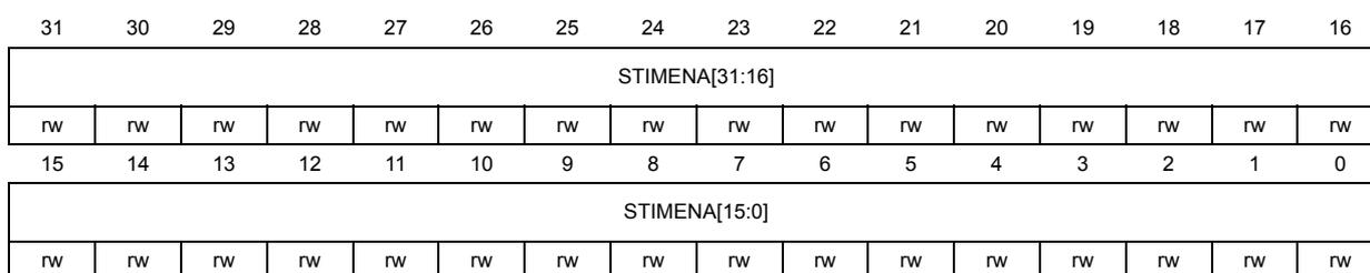
| 31 | 30 | 29 | 28 | 27 | 26 | 25 | 24 | 23 | 22 | 21 | 20 | 19 | 18 | 17 | 16 |
| STIMENA[31:16] | |||||||||||||||
| rw | rw | rw | rw | rw | rw | rw | rw | rw | rw | rw | rw | rw | rw | rw | rw |
| 15 | 14 | 13 | 12 | 11 | 10 | 9 | 8 | 7 | 6 | 5 | 4 | 3 | 2 | 1 | 0 |
| STIMENA[15:0] | |||||||||||||||
| rw | rw | rw | rw | rw | rw | rw | rw | rw | rw | rw | rw | rw | rw | rw | rw |
Bits 31:0 STIMENA[31:0] : Enable for stimulus port
Each bit x enables the stimulus port associated with the ITM_STIMRx register.
0: Port disabled
1: Port enabled
43.8.4 ITM trace privilege register (ITM_TPR)
Address offset: 0xE40
Reset value: 0x0000 0000
| 31 | 30 | 29 | 28 | 27 | 26 | 25 | 24 | 23 | 22 | 21 | 20 | 19 | 18 | 17 | 16 |
| Res. | Res. | Res. | Res. | Res. | Res. | Res. | Res. | Res. | Res. | Res. | Res. | Res. | Res. | Res. | Res. |
| 15 | 14 | 13 | 12 | 11 | 10 | 9 | 8 | 7 | 6 | 5 | 4 | 3 | 2 | 1 | 0 |
| Res. | Res. | Res. | Res. | Res. | Res. | Res. | Res. | Res. | Res. | Res. | Res. | PRIVMASK[3:0] | |||
| r | r | r | r | ||||||||||||
Bits 31:4 Reserved, must be kept at reset value.
Bits 3:0 PRIVMASK[3:0] : Enables unprivileged access to ITM stimulus ports.
Each bit controls eight stimulus ports.
0bXXX0: Unprivileged access permitted on ports 0 to 7
0bXXX1: Only privileged access permitted on ports 0 to 7
0bXX0X: Unprivileged access permitted on ports 8 to 15
0bXX1X: Only privileged access permitted on ports 8 to 15
0bX0XX: Unprivileged access permitted on ports 16 to 23
0bX1XX: Only privileged access permitted on ports 16 to 23
0b0XXX: Unprivileged access permitted on ports 24 to 31
0b1XXX: Only privileged access permitted on ports 24 to 31.
43.8.5 ITM trace control register (ITM_TCR)
Address offset: 0xE80
Reset value: 0x0000 0000
| 31 | 30 | 29 | 28 | 27 | 26 | 25 | 24 | 23 | 22 | 21 | 20 | 19 | 18 | 17 | 16 |
|---|---|---|---|---|---|---|---|---|---|---|---|---|---|---|---|
| Res. | Res. | Res. | Res. | Res. | Res. | Res. | Res. | BUSY | TRACEBUSID[6:0] | ||||||
| r | rw | rw | rw | rw | rw | rw | rw | ||||||||
| 15 | 14 | 13 | 12 | 11 | 10 | 9 | 8 | 7 | 6 | 5 | 4 | 3 | 2 | 1 | 0 |
| Res. | Res. | Res. | Res. | Res. | Res. | TSPRESCALE[1:0] | Res. | Res. | STALL ENA | SWOENA | TXENA | SYNCENA | TSENA | ITMENA | |
| rw | rw | rw | r | rw | rw | rw | rw | ||||||||
Bits 31:24 Reserved, must be kept at reset value.
Bit 23 BUSY : Indicates whether the ITM is currently processing events.
0: Not busy
1: Busy
Bits 22:16 TRACEBUSID[6:0] : identifier for multi-source trace stream formatting
If multi-source trace is in use, the debugger must write a non-zero value to this field.
Note: Different IDs must be used for each trace source in the system.
Bits 15:10 Reserved, must be kept at reset value.
Bits 9:8 TSPRESCALE[1:0] : local timestamp prescaler
Used with the trace packet reference clock. The possible values are:
0x0: No prescaling
0x1: Divides by 4.
0x2: Divides by 16.
0x3: Divides by 64.
Bits 7:6 Reserved, must be kept at reset value.
Bit 5 STALLENA : Stall enable
0: Drop hardware source packets and generate an overflow if the ITM output is stalled.
1: Stall the processor to guarantee delivery of the data trace packets.
Bit 4 SWOENA : Enable for asynchronous clocking of the timestamp counter (read only)
0: Timestamp counter uses processor clock
Bit 3 TXENA : Enables forwarding of hardware event packets from the DWT unit to the trace port.
0: Disabled
1: Enabled
Bit 2 SYNCENA : Enable for packet transmission synchronization
Note: The debugger setting this bit must also configure the DWT_CTRLR register SYNCTAP field in the DWT for the correct synchronization speed.
0: Disabled
1: Enabled
Bit 1 TSENA : Enable for local timestamp generation
0: Disabled
1: Enabled
Bit 0 ITMENA : ITM enable
0: Disabled
1: Enabled
43.8.6 ITM device type architecture register (ITM_DEVARCHR)
Address offset: 0xFBC
Reset value: 0x4770 1A01
| 31 | 30 | 29 | 28 | 27 | 26 | 25 | 24 | 23 | 22 | 21 | 20 | 19 | 18 | 17 | 16 |
|---|---|---|---|---|---|---|---|---|---|---|---|---|---|---|---|
| ARCHITECT[10:0] | PRESENT | REVISION[3:0] | |||||||||||||
| r | r | r | r | r | r | r | r | r | r | r | r | r | r | r | r |
| 15 | 14 | 13 | 12 | 11 | 10 | 9 | 8 | 7 | 6 | 5 | 4 | 3 | 2 | 1 | 0 |
| ARCHVER[3:0] | ARCHPART[11:0] | ||||||||||||||
| r | r | r | r | r | r | r | r | r | r | r | r | r | r | r | r |
Bits 31:21 ARCHITECT[10:0] : Architect JEP106 code
0x23B: JEP106 continuation code 0x4, JEP106 ID code 0x3B Arm ® .
Bit 20 PRESENT : DWT_DEVARCH register present
0x1: Present.
Bits 19:16 REVISION[3:0] : Architecture revision
0x0: DWT architecture v2.0.
Bits 15:12 ARCHVER[3:0] : Architecture version
0x1: DWT architecture v2.0.
Bits 11:0 ARCHPART[11:0] : Architecture part
0xA01: DWT architecture
43.8.7 ITM device type register 4 (ITM_DEVTYPE)
Address offset: 0xFCC
Reset value: 0x0000 0043
| 31 | 30 | 29 | 28 | 27 | 26 | 25 | 24 | 23 | 22 | 21 | 20 | 19 | 18 | 17 | 16 |
|---|---|---|---|---|---|---|---|---|---|---|---|---|---|---|---|
| Res. | Res. | Res. | Res. | Res. | Res. | Res. | Res. | Res. | Res. | Res. | Res. | Res. | Res. | Res. | Res. |
| 15 | 14 | 13 | 12 | 11 | 10 | 9 | 8 | 7 | 6 | 5 | 4 | 3 | 2 | 1 | 0 |
| Res. | Res. | Res. | Res. | Res. | Res. | Res. | Res. | SUB[3:0] | MAJOR[3:0] | ||||||
| r | r | r | r | r | r | r | r | ||||||||
Bits 31:8 Reserved, must be kept at reset value.
Bits 7:4 SUB[3:0] : Sub-type
0x4: associated with a bus, stimulus derived from bus activity
Bits 3:0
MAJOR[3:0]
: Major type
0x3: trace source
43.8.8 ITM CoreSight peripheral identity register 4 (ITM_PIDR4)
Address offset: 0xFD0
Reset value: 0x0000 0004
| 31 | 30 | 29 | 28 | 27 | 26 | 25 | 24 | 23 | 22 | 21 | 20 | 19 | 18 | 17 | 16 |
|---|---|---|---|---|---|---|---|---|---|---|---|---|---|---|---|
| Res. | Res. | Res. | Res. | Res. | Res. | Res. | Res. | Res. | Res. | Res. | Res. | Res. | Res. | Res. | Res. |
| 15 | 14 | 13 | 12 | 11 | 10 | 9 | 8 | 7 | 6 | 5 | 4 | 3 | 2 | 1 | 0 |
| Res. | Res. | Res. | Res. | Res. | Res. | Res. | Res. | F4KCOUNT[3:0] | JEP106CON[3:0] | ||||||
| r | r | r | r | r | r | r | r | ||||||||
Bits 31:8 Reserved, must be kept at reset value.
Bits 7:4
F4KCOUNT[3:0]
: Register file size
0x0: Register file occupies a single 4-Kbyte region.
Bits 3:0
JEP106CON[3:0]
: JEP106 continuation code
0x4: Arm
®
JEDEC code
43.8.9 ITM CoreSight peripheral identity register 0 (ITM_PIDR0)
Address offset: 0xFE0
Reset value: 0x0000 0021
| 31 | 30 | 29 | 28 | 27 | 26 | 25 | 24 | 23 | 22 | 21 | 20 | 19 | 18 | 17 | 16 |
|---|---|---|---|---|---|---|---|---|---|---|---|---|---|---|---|
| Res. | Res. | Res. | Res. | Res. | Res. | Res. | Res. | Res. | Res. | Res. | Res. | Res. | Res. | Res. | Res. |
| 15 | 14 | 13 | 12 | 11 | 10 | 9 | 8 | 7 | 6 | 5 | 4 | 3 | 2 | 1 | 0 |
| Res. | Res. | Res. | Res. | Res. | Res. | Res. | Res. | PARTNUM[7:0] | |||||||
| r | r | r | r | r | r | r | r | ||||||||
Bits 31:8 Reserved, must be kept at reset value.
Bits 7:0
PARTNUM[7:0]
: Part number bits [7:0]
0x21: ITM part number
43.8.10 ITM CoreSight peripheral identity register 1 (ITM_PIDR1)
Address offset: 0xFE4
Reset value: 0x0000 00BD
| 31 | 30 | 29 | 28 | 27 | 26 | 25 | 24 | 23 | 22 | 21 | 20 | 19 | 18 | 17 | 16 |
|---|---|---|---|---|---|---|---|---|---|---|---|---|---|---|---|
| Res. | Res. | Res. | Res. | Res. | Res. | Res. | Res. | Res. | Res. | Res. | Res. | Res. | Res. | Res. | Res. |
| 15 | 14 | 13 | 12 | 11 | 10 | 9 | 8 | 7 | 6 | 5 | 4 | 3 | 2 | 1 | 0 |
| Res. | Res. | Res. | Res. | Res. | Res. | Res. | Res. | JEP106ID[3:0] | PARTNUM[11:8] | ||||||
| r | r | r | r | r | r | r | r | ||||||||
Bits 31:8 Reserved, must be kept at reset value.
Bits 7:4 JEP106ID[3:0] : JEP106 identity code bits [3:0]
0xB: Arm® JEDEC code
Bits 3:0 PARTNUM[11:8] : Part number bits [11:8]
0xD: ITM part number
43.8.11 ITM CoreSight peripheral identity register 2 (ITM_PIDR2)
Address offset: 0xFE8
Reset value: 0x0000 000B
| 31 | 30 | 29 | 28 | 27 | 26 | 25 | 24 | 23 | 22 | 21 | 20 | 19 | 18 | 17 | 16 |
|---|---|---|---|---|---|---|---|---|---|---|---|---|---|---|---|
| Res. | Res. | Res. | Res. | Res. | Res. | Res. | Res. | Res. | Res. | Res. | Res. | Res. | Res. | Res. | Res. |
| 15 | 14 | 13 | 12 | 11 | 10 | 9 | 8 | 7 | 6 | 5 | 4 | 3 | 2 | 1 | 0 |
| Res. | Res. | Res. | Res. | Res. | Res. | Res. | Res. | REVISION[3:0] | JEDEC | JEP106ID[6:4] | |||||
| r | r | r | r | r | r | r | r | ||||||||
Bits 31:8 Reserved, must be kept at reset value.
Bits 7:4 REVISION[3:0] : Component revision number
0x0: r0p0
Bit 3 JEDEC : JEDEC assigned value
0x1: Designer ID specified by JEDEC
Bits 2:0 JEP106ID[6:4] : JEP106 identity code bits [6:4]
0x3: Arm® JEDEC code
43.8.12 ITM CoreSight peripheral identity register 3 (ITM_PIDR3)
Address offset: 0xFEC
Reset value: 0x0000 0000
| 31 | 30 | 29 | 28 | 27 | 26 | 25 | 24 | 23 | 22 | 21 | 20 | 19 | 18 | 17 | 16 |
|---|---|---|---|---|---|---|---|---|---|---|---|---|---|---|---|
| Res. | Res. | Res. | Res. | Res. | Res. | Res. | Res. | Res. | Res. | Res. | Res. | Res. | Res. | Res. | Res. |
| 15 | 14 | 13 | 12 | 11 | 10 | 9 | 8 | 7 | 6 | 5 | 4 | 3 | 2 | 1 | 0 |
| Res. | Res. | Res. | Res. | Res. | Res. | Res. | Res. | REVAND[3:0] | CMOD[3:0] | ||||||
| r | r | r | r | r | r | r | r | ||||||||
Bits 31:8 Reserved, must be kept at reset value.
Bits 7:4 REVAND[3:0] : Metal fix version
0x0: No metal fix
Bits 3:0 CMOD[3:0] : Customer modified
0x0: No customer modifications
43.8.13 ITM CoreSight component identity register 0 (ITM_CIDR0)
Address offset: 0xFF0
Reset value: 0x0000 000D
| 31 | 30 | 29 | 28 | 27 | 26 | 25 | 24 | 23 | 22 | 21 | 20 | 19 | 18 | 17 | 16 |
|---|---|---|---|---|---|---|---|---|---|---|---|---|---|---|---|
| Res. | Res. | Res. | Res. | Res. | Res. | Res. | Res. | Res. | Res. | Res. | Res. | Res. | Res. | Res. | Res. |
| 15 | 14 | 13 | 12 | 11 | 10 | 9 | 8 | 7 | 6 | 5 | 4 | 3 | 2 | 1 | 0 |
| Res. | Res. | Res. | Res. | Res. | Res. | Res. | Res. | PREAMBLE[7:0] | |||||||
| r | r | r | r | r | r | r | r | ||||||||
Bits 31:8 Reserved, must be kept at reset value.
Bits 7:0 PREAMBLE[7:0] : Component ID bits [7:0]
0x0D: Common ID value
43.8.14 ITM CoreSight peripheral identity register 1 (ITM_CIDR1)
Address offset: 0xFF4
Reset value: 0x0000 00E0
| 31 | 30 | 29 | 28 | 27 | 26 | 25 | 24 | 23 | 22 | 21 | 20 | 19 | 18 | 17 | 16 |
|---|---|---|---|---|---|---|---|---|---|---|---|---|---|---|---|
| Res. | Res. | Res. | Res. | Res. | Res. | Res. | Res. | Res. | Res. | Res. | Res. | Res. | Res. | Res. | Res. |
| 15 | 14 | 13 | 12 | 11 | 10 | 9 | 8 | 7 | 6 | 5 | 4 | 3 | 2 | 1 | 0 |
| Res. | Res. | Res. | Res. | Res. | Res. | Res. | Res. | ||||||||
| CLASS[3:0] | PREAMBLE[11:8] | ||||||||||||||
| r | r | r | r | r | r | r | r | ||||||||
Bits 31:8 Reserved, must be kept at reset value.
Bits 7:4
CLASS[3:0]
: Component ID bits [15:12] - component class
0xE: Trace generator component
Bits 3:0
PREAMBLE[11:8]
: Component ID bits [11:8]
0x0: Common ID value
43.8.15 ITM CoreSight component identity register 2 (ITM_CIDR2)
Address offset: 0xFF8
Reset value: 0x0000 0005
| 31 | 30 | 29 | 28 | 27 | 26 | 25 | 24 | 23 | 22 | 21 | 20 | 19 | 18 | 17 | 16 |
|---|---|---|---|---|---|---|---|---|---|---|---|---|---|---|---|
| Res. | Res. | Res. | Res. | Res. | Res. | Res. | Res. | Res. | Res. | Res. | Res. | Res. | Res. | Res. | Res. |
| 15 | 14 | 13 | 12 | 11 | 10 | 9 | 8 | 7 | 6 | 5 | 4 | 3 | 2 | 1 | 0 |
| Res. | Res. | Res. | Res. | Res. | Res. | Res. | Res. | ||||||||
| PREAMBLE[19:12] | |||||||||||||||
| r | r | r | r | r | r | r | r | ||||||||
Bits 31:8 Reserved, must be kept at reset value.
Bits 7:0
PREAMBLE[19:12]
: Component ID bits [23:16]
0x05: Common ID value
Address offset: 0xFFC
Reset value: 0x0000 00B1
| 31 | 30 | 29 | 28 | 27 | 26 | 25 | 24 | 23 | 22 | 21 | 20 | 19 | 18 | 17 | 16 |
|---|---|---|---|---|---|---|---|---|---|---|---|---|---|---|---|
| Res. | Res. | Res. | Res. | Res. | Res. | Res. | Res. | Res. | Res. | Res. | Res. | Res. | Res. | Res. | Res. |
| 15 | 14 | 13 | 12 | 11 | 10 | 9 | 8 | 7 | 6 | 5 | 4 | 3 | 2 | 1 | 0 |
| Res. | Res. | Res. | Res. | Res. | Res. | Res. | Res. | PREAMBLE[27:20] | |||||||
| r | r | r | r | r | r | r | r | ||||||||
Bits 31:8 Reserved, must be kept at reset value.
Bits 7:0 PREAMBLE[27:20] : Component ID bits [31:24]0xB1: Common ID value
43.8.17 ITM register map and reset values
Table 431. ITM register map and reset values
| Offset | Register name | 31 | 30 | 29 | 28 | 27 | 26 | 25 | 24 | 23 | 22 | 21 | 20 | 19 | 18 | 17 | 16 | 15 | 14 | 13 | 12 | 11 | 10 | 9 | 8 | 7 | 6 | 5 | 4 | 3 | 2 | 1 | 0 |
|---|---|---|---|---|---|---|---|---|---|---|---|---|---|---|---|---|---|---|---|---|---|---|---|---|---|---|---|---|---|---|---|---|---|
| 0x000 to 0x07C | ITM_STIMR0 to ITM_STIMR31 | STIMULUS[31:0] | |||||||||||||||||||||||||||||||
| Reset value | X | X | X | X | X | X | X | X | X | X | X | X | X | X | X | X | X | X | X | X | X | X | X | X | X | X | X | X | X | X | X | X | |
| 0x080 to 0xDFC | Reserved | Reserved. | |||||||||||||||||||||||||||||||
| 0xE00 | ITM_TER | STIMENA[31:0] | |||||||||||||||||||||||||||||||
| Reset value | 0 | 0 | 0 | 0 | 0 | 0 | 0 | 0 | 0 | 0 | 0 | 0 | 0 | 0 | 0 | 0 | 0 | 0 | 0 | 0 | 0 | 0 | 0 | 0 | 0 | 0 | 0 | 0 | 0 | 0 | 0 | 0 | |
| 0xE04 to 0xE3C | Reserved | Reserved. | |||||||||||||||||||||||||||||||
| 0xE40 | ITM_TPR | Res. | Res. | Res. | Res. | Res. | Res. | Res. | Res. | Res. | Res. | Res. | Res. | Res. | Res. | Res. | Res. | Res. | Res. | Res. | Res. | Res. | Res. | Res. | Res. | Res. | Res. | Res. | Res. | PRIVMASK [3:0] | |||
| Reset value | 0 | 0 | 0 | 0 | |||||||||||||||||||||||||||||
| 0xE44 to 0xE7C | Reserved | Reserved. | |||||||||||||||||||||||||||||||
| 0xE80 | ITM_TCR | Res. | Res. | Res. | Res. | Res. | Res. | Res. | Res. | BUSY | TRACEBUSID[6:0] | Res. | Res. | Res. | Res. | Res. | Res. | TSPRESCALE [1:0] | Res. | Res. | STALLENA | SWOENA | TXENA | SYNCENA | TSENA | ITMENA | |||||||
| Reset value | 0 | 0 | 0 | 0 | 0 | 0 | 0 | 0 | 0 | 0 | 0 | 0 | 0 | 0 | 0 | ||||||||||||||||||
| 0xE84 to 0xFB8 | Reserved | Reserved. | |||||||||||||||||||||||||||||||
| 0xFBC | DWT_DEVARCHR | ARCHITECT[10:0] | PRESEN | REVISION [3:0] | ARCHVER [3:0] | ARCHPART[11:0] | |||||||||||||||||||||||||||
| Reset value | 0 | 1 | 0 | 0 | 0 | 1 | 1 | 1 | 0 | 1 | 1 | 1 | 0 | 0 | 0 | 0 | 0 | 0 | 0 | 1 | 1 | 0 | 1 | 0 | 0 | 0 | 0 | 0 | 0 | 0 | 0 | 1 | |
| 0xFC0 to 0xFC8 | Reserved | Reserved. | |||||||||||||||||||||||||||||||
| 0xFCC | DWT_DEVTYPER | Res. | Res. | Res. | Res. | Res. | Res. | Res. | Res. | Res. | Res. | Res. | Res. | Res. | Res. | Res. | Res. | Res. | Res. | Res. | Res. | Res. | Res. | Res. | Res. | SUB[3:0] | MAJOR[3:0] | ||||||
| Reset value | 0 | 1 | 0 | 0 | 0 | 0 | 1 | 1 | |||||||||||||||||||||||||
| 0xFD0 | ITM_PIDR4 | Res. | Res. | Res. | Res. | Res. | Res. | Res. | Res. | Res. | Res. | Res. | Res. | Res. | Res. | Res. | Res. | Res. | Res. | Res. | Res. | Res. | Res. | Res. | Res. | F4KCOUNT [3:0] | JEP106CON [3:0] | ||||||
| Reset value | 0 | 0 | 0 | 0 | 0 | 1 | 0 | 0 | |||||||||||||||||||||||||
| 0xFD4 to 0xFDC | Reserved | Reserved. | |||||||||||||||||||||||||||||||
| 0xFE0 | ITM_PIDR0 | Res. | Res. | Res. | Res. | Res. | Res. | Res. | Res. | Res. | Res. | Res. | Res. | Res. | Res. | Res. | Res. | Res. | Res. | Res. | Res. | Res. | Res. | Res. | Res. | PARTNUM[7:0] | |||||||
| Reset value | 0 | 0 | 1 | 0 | 0 | 0 | 0 | 1 | |||||||||||||||||||||||||
| 0xFE4 | ITM_PIDR1 | Res. | Res. | Res. | Res. | Res. | Res. | Res. | Res. | Res. | Res. | Res. | Res. | Res. | Res. | Res. | Res. | Res. | Res. | Res. | Res. | Res. | Res. | Res. | Res. | JEP106ID [3:0] | PARTNUM [11:8] | ||||||
| Reset value | 1 | 0 | 1 | 1 | 1 | 1 | 0 | 1 | |||||||||||||||||||||||||
| 0xFE8 | ITM_PIDR2 | Res. | Res. | Res. | Res. | Res. | Res. | Res. | Res. | Res. | Res. | Res. | Res. | Res. | Res. | Res. | Res. | Res. | Res. | Res. | Res. | Res. | Res. | Res. | Res. | REVISION [3:0] | JEDEC | JEP106ID [6:4] | |||||
| Reset value | 0 | 0 | 0 | 0 | 1 | 0 | 1 | 1 | |||||||||||||||||||||||||
| 0xFEC | ITM_PIDR3 | Res. | Res. | Res. | Res. | Res. | Res. | Res. | Res. | Res. | Res. | Res. | Res. | Res. | Res. | Res. | Res. | Res. | Res. | Res. | Res. | Res. | Res. | Res. | Res. | REVAND[3:0] | CMOD[3:0] | ||||||
| Reset value | 0 | 0 | 0 | 0 | 0 | 0 | 0 | 0 | |||||||||||||||||||||||||
| 0xFF0 | ITM_CIDR0 | Res. | Res. | Res. | Res. | Res. | Res. | Res. | Res. | Res. | Res. | Res. | Res. | Res. | Res. | Res. | Res. | Res. | Res. | Res. | Res. | Res. | Res. | Res. | Res. | PREAMBLE[7:0] | |||||||
| Reset value | 0 | 0 | 0 | 0 | 1 | 1 | 0 | 1 | |||||||||||||||||||||||||
Table 431. ITM register map and reset values (continued)
| Offset | Register name | 31 | 30 | 29 | 28 | 27 | 26 | 25 | 24 | 23 | 22 | 21 | 20 | 19 | 18 | 17 | 16 | 15 | 14 | 13 | 12 | 11 | 10 | 9 | 8 | 7 | 6 | 5 | 4 | 3 | 2 | 1 | 0 |
|---|---|---|---|---|---|---|---|---|---|---|---|---|---|---|---|---|---|---|---|---|---|---|---|---|---|---|---|---|---|---|---|---|---|
| 0xFF4 | ITM_CIDR1 | Res. | Res. | Res. | Res. | Res. | Res. | Res. | Res. | Res. | Res. | Res. | Res. | Res. | Res. | Res. | Res. | Res. | Res. | Res. | Res. | Res. | Res. | Res. | Res. | CLASS[3:0] | PREAMBLE [11:8] | ||||||
| Reset value | 1 | 1 | 1 | 0 | 0 | 0 | 0 | 0 | 0 | ||||||||||||||||||||||||
| 0xFF8 | ITM_CIDR2 | Res. | Res. | Res. | Res. | Res. | Res. | Res. | Res. | Res. | Res. | Res. | Res. | Res. | Res. | Res. | Res. | Res. | Res. | Res. | Res. | Res. | Res. | Res. | PREAMBLE[19:12] | ||||||||
| Reset value | 0 | 0 | 0 | 0 | 0 | 1 | 0 | 1 | |||||||||||||||||||||||||
| 0xFFC | ITM_CIDR3 | Res. | Res. | Res. | Res. | Res. | Res. | Res. | Res. | Res. | Res. | Res. | Res. | Res. | Res. | Res. | Res. | Res. | Res. | Res. | Res. | Res. | Res. | Res. | PREAMBLE[27:20] | ||||||||
| Reset value | 1 | 0 | 1 | 1 | 0 | 0 | 0 | 1 | |||||||||||||||||||||||||
Refer to Section 43.5: System debug AP0 features for the register boundary addresses.
43.9 Breakpoint unit (BPU)
The BPU allows hardware breakpoints to be set. It contains eight comparators that monitor the instruction fetch address. If a match occurs, the instruction comparators can be configured to generate a breakpoint instruction.
For more information on the BPU and how to use it, refer to the Armv8-M Architecture Reference Manual [4].
43.9.1 BPU control register (BPU_CTRLR)
Address offset: 0x000
Reset value: 0x1000 0080
| 31 | 30 | 29 | 28 | 27 | 26 | 25 | 24 | 23 | 22 | 21 | 20 | 19 | 18 | 17 | 16 |
|---|---|---|---|---|---|---|---|---|---|---|---|---|---|---|---|
| REV[3:0] | Res. | Res. | Res. | Res. | Res. | Res. | Res. | Res. | Res. | Res. | Res. | Res. | |||
| r | r | r | r | ||||||||||||
| 15 | 14 | 13 | 12 | 11 | 10 | 9 | 8 | 7 | 6 | 5 | 4 | 3 | 2 | 1 | 0 |
|---|---|---|---|---|---|---|---|---|---|---|---|---|---|---|---|
| Res. | NUM_CODE[6:4] | Res. | Res. | Res. | Res. | NUM_CODE[3:0] | Res. | Res. | KEY | ENABLE | |||||
| r | r | r | r | r | r | r | rw | rw | |||||||
Bits 31:28
REV[3:0]
: Revision number
0x1: BPU version 2
Bits 27:15 Reserved, must be kept at reset value.
Bits 14:12, 7:4
NUM_CODE[6:0]
: Number of instruction address comparators supported - least significant bits
0x8: 8 instruction comparators supported
Bits 11:8, 3:2 Reserved, must be kept at reset value.
Bit 1
KEY
: write protect key
A write to BPU_CTRLR register is ignored if this bit is not set to 1.
Bit 0
ENABLE
: BPU enable
0: Disabled
1: Enabled
43.9.2 BPU comparator x register (BPU_COMPxR)
Address offset: 0x008 + 0x4 * x, (x = 0 to 7)
Reset value: 0x0000 0000
| 31 | 30 | 29 | 28 | 27 | 26 | 25 | 24 | 23 | 22 | 21 | 20 | 19 | 18 | 17 | 16 |
|---|---|---|---|---|---|---|---|---|---|---|---|---|---|---|---|
| BPADDR[31:16] | |||||||||||||||
| rw | rw | rw | rw | rw | rw | rw | rw | rw | rw | rw | rw | rw | rw | rw | rw |
| 15 | 14 | 13 | 12 | 11 | 10 | 9 | 8 | 7 | 6 | 5 | 4 | 3 | 2 | 1 | 0 |
|---|---|---|---|---|---|---|---|---|---|---|---|---|---|---|---|
| BPADDR[15:1] | BE | ||||||||||||||
| rw | rw | rw | rw | rw | rw | rw | rw | rw | rw | rw | rw | rw | rw | rw | rw |
Bits 31:1 BPADDR[31:1] : Breakpoint address
Bit 0 BE : Breakpoint enable
0: disabled
1: enabled
43.9.3 BPU device type architecture register (BPU_DEVARCHR)
Address offset: 0xFBC
Reset value: 0x4770 1A03
| 31 | 30 | 29 | 28 | 27 | 26 | 25 | 24 | 23 | 22 | 21 | 20 | 19 | 18 | 17 | 16 |
|---|---|---|---|---|---|---|---|---|---|---|---|---|---|---|---|
| ARCHITECT[10:0] | PRESENT | REVISION[3:0] | |||||||||||||
| r | r | r | r | r | r | r | r | r | r | r | r | r | r | r | r |
| 15 | 14 | 13 | 12 | 11 | 10 | 9 | 8 | 7 | 6 | 5 | 4 | 3 | 2 | 1 | 0 |
| ARCHVER[3:0] | ARCHPART[11:0] | ||||||||||||||
| r | r | r | r | r | r | r | r | r | r | r | r | r | r | r | r |
Bits 31:21 ARCHITECT[10:0] : Architect JEP106 code
0x23B: JEP106 continuation code 0x4, JEP106 ID code 0x3B Arm ® .
Bit 20 PRESENT : DEVARCH register present
0x1: Present.
Bits 19:16 REVISION[3:0] : Architecture revision
0x0: BPU architecture v2.0.
Bits 15:12 ARCHVER[3:0] : Architecture version
0x1: BPU architecture v2.0.
Bits 11:0 ARCHPART[11:0] : Architecture part
0xA03: BPU architecture
43.9.4 BPU device type register 4 (BPU_DEVTYPE4)
Address offset: 0xFCC
Reset value: 0x0000 0000
| 31 | 30 | 29 | 28 | 27 | 26 | 25 | 24 | 23 | 22 | 21 | 20 | 19 | 18 | 17 | 16 |
|---|---|---|---|---|---|---|---|---|---|---|---|---|---|---|---|
| Res. | Res. | Res. | Res. | Res. | Res. | Res. | Res. | Res. | Res. | Res. | Res. | Res. | Res. | Res. | Res. |
| 15 | 14 | 13 | 12 | 11 | 10 | 9 | 8 | 7 | 6 | 5 | 4 | 3 | 2 | 1 | 0 |
| Res. | Res. | Res. | Res. | Res. | Res. | Res. | Res. | SUB[3:0] | MAJOR[3:0] | ||||||
| r | r | r | r | r | r | r | r | ||||||||
Bits 31:8 Reserved, must be kept at reset value.
Bits 7:4 SUB[3:0] : Sub-type
0x0: other
Bits 3:0
MAJOR[3:0]
: major type
0x0: miscellaneous
43.9.5 BPU CoreSight peripheral identity register 4 (BPU_PIDR4)
Address offset: 0xFD0
Reset value: 0x0000 0004
| 31 | 30 | 29 | 28 | 27 | 26 | 25 | 24 | 23 | 22 | 21 | 20 | 19 | 18 | 17 | 16 |
|---|---|---|---|---|---|---|---|---|---|---|---|---|---|---|---|
| Res. | Res. | Res. | Res. | Res. | Res. | Res. | Res. | Res. | Res. | Res. | Res. | Res. | Res. | Res. | Res. |
| 15 | 14 | 13 | 12 | 11 | 10 | 9 | 8 | 7 | 6 | 5 | 4 | 3 | 2 | 1 | 0 |
| Res. | Res. | Res. | Res. | Res. | Res. | Res. | Res. | F4KCOUNT[3:0] | JEP106CON[3:0] | ||||||
| r | r | r | r | r | r | r | r | ||||||||
Bits 31:8 Reserved, must be kept at reset value.
Bits 7:4
F4KCOUNT[3:0]
: register file size
0x0: Register file occupies a single 4-Kbyte region.
Bits 3:0
JEP106CON[3:0]
: JEP106 continuation code
0x4: Arm® JEDEC code
43.9.6 BPU CoreSight peripheral identity register 0 (BPU_PIDR0)
Address offset: 0xFE0
Reset value: 0x0000 0021
| 31 | 30 | 29 | 28 | 27 | 26 | 25 | 24 | 23 | 22 | 21 | 20 | 19 | 18 | 17 | 16 |
|---|---|---|---|---|---|---|---|---|---|---|---|---|---|---|---|
| Res. | Res. | Res. | Res. | Res. | Res. | Res. | Res. | Res. | Res. | Res. | Res. | Res. | Res. | Res. | Res. |
| 15 | 14 | 13 | 12 | 11 | 10 | 9 | 8 | 7 | 6 | 5 | 4 | 3 | 2 | 1 | 0 |
| Res. | Res. | Res. | Res. | Res. | Res. | Res. | Res. | PARTNUM[7:0] | |||||||
| r | r | r | r | r | r | r | r | ||||||||
Bits 31:8 Reserved, must be kept at reset value.
Bits 7:0
PARTNUM[7:0]
: Part number bits [7:0]
0x21: BPU part number
43.9.7 BPU CoreSight peripheral identity register 1 (BPU_PIDR1)
Address offset: 0xFE4
Reset value: 0x0000 00BD
| 31 | 30 | 29 | 28 | 27 | 26 | 25 | 24 | 23 | 22 | 21 | 20 | 19 | 18 | 17 | 16 |
|---|---|---|---|---|---|---|---|---|---|---|---|---|---|---|---|
| Res. | Res. | Res. | Res. | Res. | Res. | Res. | Res. | Res. | Res. | Res. | Res. | Res. | Res. | Res. | Res. |
| 15 | 14 | 13 | 12 | 11 | 10 | 9 | 8 | 7 | 6 | 5 | 4 | 3 | 2 | 1 | 0 |
| Res. | Res. | Res. | Res. | Res. | Res. | Res. | Res. | JEP106ID[3:0] | PARTNUM[11:8] | ||||||
| r | r | r | r | r | r | r | r | ||||||||
Bits 31:8 Reserved, must be kept at reset value.
Bits 7:4 JEP106ID[3:0] : JEP106 identity code bits [3:0]
0xB: Arm® JEDEC code
Bits 3:0 PARTNUM[11:8] : Part number bits [11:8]
0xD: BPU part number
43.9.8 BPU CoreSight peripheral identity register 2 (BPU_PIDR2)
Address offset: 0xFE8
Reset value: 0x0000 000B
| 31 | 30 | 29 | 28 | 27 | 26 | 25 | 24 | 23 | 22 | 21 | 20 | 19 | 18 | 17 | 16 |
|---|---|---|---|---|---|---|---|---|---|---|---|---|---|---|---|
| Res. | Res. | Res. | Res. | Res. | Res. | Res. | Res. | Res. | Res. | Res. | Res. | Res. | Res. | Res. | Res. |
| 15 | 14 | 13 | 12 | 11 | 10 | 9 | 8 | 7 | 6 | 5 | 4 | 3 | 2 | 1 | 0 |
| Res. | Res. | Res. | Res. | Res. | Res. | Res. | Res. | REVISION[3:0] | JEDEC | JEP106ID[6:4] | |||||
| r | r | r | r | r | r | r | r | ||||||||
Bits 31:8 Reserved, must be kept at reset value.
Bits 7:4 REVISION[3:0] : Component revision number
0x0: r0p0
Bit 3 JEDEC : JEDEC assigned value
1: Designer ID specified by JEDEC
Bits 2:0 JEP106ID[6:4] : JEP106 identity code bits [6:4]
0x3: Arm® JEDEC code
43.9.9 BPU CoreSight peripheral identity register 3 (BPU_PIDR3)
Address offset: 0xFEC
Reset value: 0x0000 0000
| 31 | 30 | 29 | 28 | 27 | 26 | 25 | 24 | 23 | 22 | 21 | 20 | 19 | 18 | 17 | 16 |
|---|---|---|---|---|---|---|---|---|---|---|---|---|---|---|---|
| Res. | Res. | Res. | Res. | Res. | Res. | Res. | Res. | Res. | Res. | Res. | Res. | Res. | Res. | Res. | Res. |
| 15 | 14 | 13 | 12 | 11 | 10 | 9 | 8 | 7 | 6 | 5 | 4 | 3 | 2 | 1 | 0 |
| Res. | Res. | Res. | Res. | Res. | Res. | Res. | Res. | ||||||||
| REVAND[3:0] | CMOD[3:0] | ||||||||||||||
| r | r | r | r | r | r | r | r | ||||||||
Bits 31:8 Reserved, must be kept at reset value.
Bits 7:4 REVAND[3:0] : Metal fix version
0x0: No metal fix
Bits 3:0 CMOD[3:0] : Customer modified
0x0: No customer modifications
43.9.10 BPU CoreSight component identity register 0 (BPU_CIDR0)
Address offset: 0xFF0
Reset value: 0x0000 000D
| 31 | 30 | 29 | 28 | 27 | 26 | 25 | 24 | 23 | 22 | 21 | 20 | 19 | 18 | 17 | 16 |
|---|---|---|---|---|---|---|---|---|---|---|---|---|---|---|---|
| Res. | Res. | Res. | Res. | Res. | Res. | Res. | Res. | Res. | Res. | Res. | Res. | Res. | Res. | Res. | Res. |
| 15 | 14 | 13 | 12 | 11 | 10 | 9 | 8 | 7 | 6 | 5 | 4 | 3 | 2 | 1 | 0 |
| Res. | Res. | Res. | Res. | Res. | Res. | Res. | Res. | ||||||||
| PREAMBLE[7:0] | |||||||||||||||
| r | r | r | r | r | r | r | r | ||||||||
Bits 31:8 Reserved, must be kept at reset value.
Bits 7:0 PREAMBLE[7:0] : Component ID bits [7:0]
0x0D: Common ID value
43.9.11 BPU CoreSight peripheral identity register 1 (BPU_CIDR1)
Address offset: 0xFF4
Reset value: 0x0000 0090
| 31 | 30 | 29 | 28 | 27 | 26 | 25 | 24 | 23 | 22 | 21 | 20 | 19 | 18 | 17 | 16 |
|---|---|---|---|---|---|---|---|---|---|---|---|---|---|---|---|
| Res. | Res. | Res. | Res. | Res. | Res. | Res. | Res. | Res. | Res. | Res. | Res. | Res. | Res. | Res. | Res. |
| 15 | 14 | 13 | 12 | 11 | 10 | 9 | 8 | 7 | 6 | 5 | 4 | 3 | 2 | 1 | 0 |
| Res. | Res. | Res. | Res. | Res. | Res. | Res. | Res. | CLASS[3:0] | PREAMBLE[11:8] | ||||||
| r | r | r | r | r | r | r | r | ||||||||
Bits 31:8 Reserved, must be kept at reset value.
Bits 7:4
CLASS[3:0]
: Component ID bits [15:12] - component class
0x9: debug component
Bits 3:0
PREAMBLE[11:8]
: Component ID bits [11:8]
0x0: Common ID value
43.9.12 BPU CoreSight component identity register 2 (BPU_CIDR2)
Address offset: 0xFF8
Reset value: 0x0000 0005
| 31 | 30 | 29 | 28 | 27 | 26 | 25 | 24 | 23 | 22 | 21 | 20 | 19 | 18 | 17 | 16 |
|---|---|---|---|---|---|---|---|---|---|---|---|---|---|---|---|
| Res. | Res. | Res. | Res. | Res. | Res. | Res. | Res. | Res. | Res. | Res. | Res. | Res. | Res. | Res. | Res. |
| 15 | 14 | 13 | 12 | 11 | 10 | 9 | 8 | 7 | 6 | 5 | 4 | 3 | 2 | 1 | 0 |
| Res. | Res. | Res. | Res. | Res. | Res. | Res. | Res. | PREAMBLE[19:12] | |||||||
| r | r | r | r | r | r | r | r | ||||||||
Bits 31:8 Reserved, must be kept at reset value.
Bits 7:0
PREAMBLE[19:12]
: Component ID bits [23:16]
0x05: Common ID value
Address offset: 0xFFC
Reset value: 0x0000 00B1
| 31 | 30 | 29 | 28 | 27 | 26 | 25 | 24 | 23 | 22 | 21 | 20 | 19 | 18 | 17 | 16 |
|---|---|---|---|---|---|---|---|---|---|---|---|---|---|---|---|
| Res. | Res. | Res. | Res. | Res. | Res. | Res. | Res. | Res. | Res. | Res. | Res. | Res. | Res. | Res. | Res. |
| 15 | 14 | 13 | 12 | 11 | 10 | 9 | 8 | 7 | 6 | 5 | 4 | 3 | 2 | 1 | 0 |
| Res. | Res. | Res. | Res. | Res. | Res. | Res. | Res. | PREAMBLE[27:20] | |||||||
| r | r | r | r | r | r | r | r | ||||||||
Bits 31:8 Reserved, must be kept at reset value.
Bits 7:0 PREAMBLE[27:20] : Component ID bits [31:24]0xB1: Common ID value
43.9.14 BPU register map and reset values
Table 432. BPU register map and reset values
| Offset | Register name | 31 | 30 | 29 | 28 | 27 | 26 | 25 | 24 | 23 | 22 | 21 | 20 | 19 | 18 | 17 | 16 | 15 | 14 | 13 | 12 | 11 | 10 | 9 | 8 | 7 | 6 | 5 | 4 | 3 | 2 | 1 | 0 |
|---|---|---|---|---|---|---|---|---|---|---|---|---|---|---|---|---|---|---|---|---|---|---|---|---|---|---|---|---|---|---|---|---|---|
| 0x000 | BPU_CTRLR | NUM_LIT [3:0] | Res. | Res. | Res. | Res. | Res. | Res. | Res. | Res. | Res. | Res. | Res. | Res. | Res. | Res. | NUM_CODE [6:4] | NUM_CODE [3:0] | Res. | Res. | KEY ENABLE | ||||||||||||
| Reset value | 0 | 0 | 0 | 1 | 0 | 0 | 0 | 1 | 0 | 0 | 0 | 0 | 0 | ||||||||||||||||||||
| 0x004 | Reserved | Reserved. | |||||||||||||||||||||||||||||||
| 0x008 to 0x024 | BPU_COMP0R to BPU_COMP7R | BPADDR[31:1] | BE | ||||||||||||||||||||||||||||||
| Reset value | 0 | 0 | 0 | 0 | 0 | 0 | 0 | 0 | 0 | 0 | 0 | 0 | 0 | 0 | 0 | 0 | 0 | 0 | 0 | 0 | 0 | 0 | 0 | 0 | 0 | 0 | 0 | 0 | 0 | 0 | 0 | 0 | |
| 0x02C- 0xFB8 | Reserved | Reserved. | |||||||||||||||||||||||||||||||
| 0xFB8 | DWT_DEVARCHR | ARCHITECT[10:0] | PRESEN | REVISION [3:0] | ARCHVER [3:0] | ARCHPART[11:0] | |||||||||||||||||||||||||||
| Reset value | 0 | 1 | 0 | 0 | 0 | 1 | 1 | 1 | 0 | 1 | 1 | 1 | 0 | 1 | 0 | 0 | 0 | 0 | 0 | 0 | 0 | 0 | 0 | 0 | 0 | 0 | 0 | 1 | 1 | ||||
| 0xFC0 to 0xFC8 | Reserved | Reserved. | |||||||||||||||||||||||||||||||
| 0xFC8 | DWT_DEVTYPE | Res. | Res. | Res. | Res. | Res. | Res. | Res. | Res. | Res. | Res. | Res. | Res. | Res. | Res. | Res. | Res. | Res. | Res. | Res. | Res. | Res. | Res. | Res. | Res. | Res. | SUB[3:0] | MAJOR[3:8] | |||||
| Reset value | 0 | 0 | 0 | 0 | 0 | 0 | 0 | ||||||||||||||||||||||||||
| 0xFD0 | BPU_PIDR4 | Res. | Res. | Res. | Res. | Res. | Res. | Res. | Res. | Res. | Res. | Res. | Res. | Res. | Res. | Res. | Res. | Res. | Res. | Res. | Res. | Res. | Res. | Res. | Res. | Res. | F4COUNT [3:0] | JEP106CON [3:0] | |||||
| Reset value | 0 | 0 | 0 | 0 | 0 | 1 | 0 | ||||||||||||||||||||||||||
| 0xFD4- 0xFDC | Reserved | Reserved. | |||||||||||||||||||||||||||||||
| 0xFE0 | BPU_PIDR0 | Res. | Res. | Res. | Res. | Res. | Res. | Res. | Res. | Res. | Res. | Res. | Res. | Res. | Res. | Res. | Res. | Res. | Res. | Res. | Res. | Res. | Res. | Res. | Res. | Res. | PARTNUM[7:0] | ||||||
| Reset value | 0 | 0 | 1 | 0 | 0 | 0 | 1 | ||||||||||||||||||||||||||
| 0xFE4 | BPU_PIDR1 | Res. | Res. | Res. | Res. | Res. | Res. | Res. | Res. | Res. | Res. | Res. | Res. | Res. | Res. | Res. | Res. | Res. | Res. | Res. | Res. | Res. | Res. | Res. | Res. | Res. | JEP106ID [3:0] | PARTNUM [11:8] | |||||
| Reset value | 1 | 0 | 1 | 1 | 1 | 1 | 0 | ||||||||||||||||||||||||||
| 0xFE8 | BPU_PIDR2 | Res. | Res. | Res. | Res. | Res. | Res. | Res. | Res. | Res. | Res. | Res. | Res. | Res. | Res. | Res. | Res. | Res. | Res. | Res. | Res. | Res. | Res. | Res. | Res. | Res. | REVISION [3:0] | JEDec | JEP106ID [6:4] | ||||
| Reset value | 0 | 0 | 0 | 0 | 1 | 0 | 1 | ||||||||||||||||||||||||||
| 0xFEC | BPU_PIDR3 | Res. | Res. | Res. | Res. | Res. | Res. | Res. | Res. | Res. | Res. | Res. | Res. | Res. | Res. | Res. | Res. | Res. | Res. | Res. | Res. | Res. | Res. | Res. | Res. | Res. | REVAND[3:0] | CMOD[3:0] | |||||
| Reset value | 0 | 0 | 0 | 0 | 0 | 0 | 0 | ||||||||||||||||||||||||||
| 0xFF0 | BPU_CIDR0 | Res. | Res. | Res. | Res. | Res. | Res. | Res. | Res. | Res. | Res. | Res. | Res. | Res. | Res. | Res. | Res. | Res. | Res. | Res. | Res. | Res. | Res. | Res. | Res. | Res. | PREAMBLE[7:0] | ||||||
| Reset value | 0 | 0 | 0 | 0 | 1 | 1 | 0 | ||||||||||||||||||||||||||
| 0xFF4 | BPU_CIDR1 | Res. | Res. | Res. | Res. | Res. | Res. | Res. | Res. | Res. | Res. | Res. | Res. | Res. | Res. | Res. | Res. | Res. | Res. | Res. | Res. | Res. | Res. | Res. | Res. | Res. | CLASS[3:0] | PREAMBLE [11:8] | |||||
| Reset value | 1 | 0 | 0 | 1 | 0 | 0 | 0 | ||||||||||||||||||||||||||
| 0xFF8 | BPU_CIDR2 | Res. | Res. | Res. | Res. | Res. | Res. | Res. | Res. | Res. | Res. | Res. | Res. | Res. | Res. | Res. | Res. | Res. | Res. | Res. | Res. | Res. | Res. | Res. | Res. | Res. | PREAMBLE[19:12] | ||||||
| Reset value | 0 | 0 | 0 | 0 | 0 | 1 | 0 | ||||||||||||||||||||||||||
| 0xFFC | BPU_CIDR3 | Res. | Res. | Res. | Res. | Res. | Res. | Res. | Res. | Res. | Res. | Res. | Res. | Res. | Res. | Res. | Res. | Res. | Res. | Res. | Res. | Res. | Res. | Res. | Res. | Res. | PREAMBLE[27:20] | ||||||
| Reset value | 1 | 0 | 1 | 1 | 0 | 0 | 1 | ||||||||||||||||||||||||||
Refer to Section 43.5: System debug AP0 features for the register boundary addresses.
43.10 Trace port interface unit (TPIU)
The TPIU formats the trace stream and outputs it on the external trace port signals. The TPIU has one ATB slave ports for incoming trace data from the ITM. The trace port is the serial-wire output, TRACESWO.
Figure 494 shows the TPIU architecture.
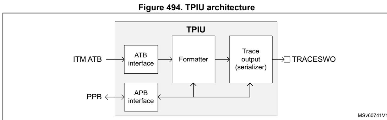
Figure 494. TPIU architecture
graph LR
    subgraph TPIU
        ATB[ATB interface] --> F[Formatter]
        APB[APB interface] --> F
        F --> TO[Trace output serializer]
    end
    ITM[ITM ATB] --> ATB
    PPB[PPB] --> APB
    TO --> TRACESWO[TRACESWO]
MSv60741V1
For more information on the TPIU and how to use it, refer to the Arm® Cortex-M33 Technical Reference Manual [5].
43.10.1 TPIU registers
43.10.2 TPIU supported port size register (TPIU_SSPSR)
Address offset: 0x000
Reset value: 0x0000 0001
| 31 | 30 | 29 | 28 | 27 | 26 | 25 | 24 | 23 | 22 | 21 | 20 | 19 | 18 | 17 | 16 |
| PORTSIZE[31:16] | |||||||||||||||
| r | r | r | r | r | r | r | r | r | r | r | r | r | r | r | r |
| 15 | 14 | 13 | 12 | 11 | 10 | 9 | 8 | 7 | 6 | 5 | 4 | 3 | 2 | 1 | 0 |
| PORTSIZE[15:0] | |||||||||||||||
| r | r | r | r | r | r | r | r | r | r | r | r | r | r | r | r |
Bits 31:0 PORTSIZE[31:0] : Supported trace port sizes, from 1 to 32 pins
Bit n-1 when set indicates that port size n is supported.
0x0000 0001: Port size 1 supported
43.10.3 TPIU current port size register (TPIU_CSPSR)
Address offset: 0x004
Reset value: 0x0000 0001
| 31 | 30 | 29 | 28 | 27 | 26 | 25 | 24 | 23 | 22 | 21 | 20 | 19 | 18 | 17 | 16 |
|---|---|---|---|---|---|---|---|---|---|---|---|---|---|---|---|
| PORTSIZE[31:16] | |||||||||||||||
| rw | rw | rw | rw | rw | rw | rw | rw | rw | rw | rw | rw | rw | rw | rw | rw |
| 15 | 14 | 13 | 12 | 11 | 10 | 9 | 8 | 7 | 6 | 5 | 4 | 3 | 2 | 1 | 0 |
| PORTSIZE[15:0] | |||||||||||||||
| rw | rw | rw | rw | rw | rw | rw | rw | rw | rw | rw | rw | rw | rw | rw | rw |
Bits 31:0 PORTSIZE[31:0] : Current trace port size
Bit n-1 when set indicates that the current port size is n pins. The value of n must be within the range of supported port size (1). Only one bit can be set, or unpredictable behavior may result. This register must be modified only when the formatter is stopped.
43.10.4 TPIU asynchronous clock prescaler register (TPIU_ACPR)
Address offset: 0x010
Reset value: 0x0000 0000
| 31 | 30 | 29 | 28 | 27 | 26 | 25 | 24 | 23 | 22 | 21 | 20 | 19 | 18 | 17 | 16 |
|---|---|---|---|---|---|---|---|---|---|---|---|---|---|---|---|
| Res. | Res. | Res. | Res. | Res. | Res. | Res. | Res. | Res. | Res. | Res. | Res. | Res. | Res. | Res. | Res. |
| 15 | 14 | 13 | 12 | 11 | 10 | 9 | 8 | 7 | 6 | 5 | 4 | 3 | 2 | 1 | 0 |
| Res. | Res. | Res. | PRESCALER[12:0] | ||||||||||||
| rw | rw | rw | rw | rw | rw | rw | rw | rw | rw | rw | rw | rw | |||
Bits 31:13 Reserved, must be kept at reset value.
Bits 12:0
PRESCALER[12:0]
: selects the baud rate for the asynchronous output, TRACESWO
The baud rate is given by the TRACECLKIN frequency divided by (PRESCALER +1).
43.10.5 TPIU selected pin protocol register (TPIU_SPPR)
Address offset: 0x0F0
Reset value: 0x0000 0001
| 31 | 30 | 29 | 28 | 27 | 26 | 25 | 24 | 23 | 22 | 21 | 20 | 19 | 18 | 17 | 16 |
|---|---|---|---|---|---|---|---|---|---|---|---|---|---|---|---|
| Res. | Res. | Res. | Res. | Res. | Res. | Res. | Res. | Res. | Res. | Res. | Res. | Res. | Res. | Res. | Res. |
| 15 | 14 | 13 | 12 | 11 | 10 | 9 | 8 | 7 | 6 | 5 | 4 | 3 | 2 | 1 | 0 |
| Res. | Res. | Res. | Res. | Res. | Res. | Res. | Res. | Res. | Res. | Res. | Res. | Res. | Res. | TXMODE[1:0] | |
| rw | rw | ||||||||||||||
Bits 31:2 Reserved, must be kept at reset value.
Bits 1:0 TXMODE[1:0] : selects the protocol used for trace output
0x0: reserved (parallel trace port mode not supported in this device)
0x1: Asynchronous SWO using Manchester encoding
0x2: Asynchronous SWO using NRZ encoding
0x3: reserved
43.10.6 TPIU formatter and flush status register (TPIU_FFSR)
Address offset: 0x300
Reset value: 0x0000 0008
| 31 | 30 | 29 | 28 | 27 | 26 | 25 | 24 | 23 | 22 | 21 | 20 | 19 | 18 | 17 | 16 |
|---|---|---|---|---|---|---|---|---|---|---|---|---|---|---|---|
| Res. | Res. | Res. | Res. | Res. | Res. | Res. | Res. | Res. | Res. | Res. | Res. | Res. | Res. | Res. | Res. |
| 15 | 14 | 13 | 12 | 11 | 10 | 9 | 8 | 7 | 6 | 5 | 4 | 3 | 2 | 1 | 0 |
| Res. | Res. | Res. | Res. | Res. | Res. | Res. | Res. | Res. | Res. | Res. | Res. | FTNON STOP | TCPRE SENT | FTSTO PPED | FLINPR OG |
| r | r | r | r |
Bits 31:4 Reserved, must be kept at reset value.
Bit 3 FTNONSTOP : Indicates whether formatter can be stopped or not
1: Formatter cannot be stopped.
Bit 2 TCPRESENT : Indicates whether the optional TRACECTL output pin is available for use
0: TRACECTL pin is not present in this device.
Bit 1 FTSTOPPED : Stop request signal received
The formatter received a stop request signal and all trace data and post-amble is sent. Any additional trace data on the ATB interface is ignored.
0: Formatter not stopped
1: Formatter stopped
Bit 0 FLINPROG : Flush in progress
This bit indicates whether a flush on the ATB slave port is in progress and reflects the status of the AFVALIDS output. A flush can be initiated by the flush control bits in the TPIU_FFCR register.
0: No flush in progress
1: Flush in progress
43.10.7 TPIU formatter and flush control register (TPIU_FFCR)
Address offset: 0x304
Reset value: 0x0000 0102
| 31 | 30 | 29 | 28 | 27 | 26 | 25 | 24 | 23 | 22 | 21 | 20 | 19 | 18 | 17 | 16 |
|---|---|---|---|---|---|---|---|---|---|---|---|---|---|---|---|
| Res. | Res. | Res. | Res. | Res. | Res. | Res. | Res. | Res. | Res. | Res. | Res. | Res. | Res. | Res. | Res. |
| 15 | 14 | 13 | 12 | 11 | 10 | 9 | 8 | 7 | 6 | 5 | 4 | 3 | 2 | 1 | 0 |
| Res. | Res. | Res. | Res. | Res. | Res. | Res. | TRIGIN | Res. | FONMAN | Res. | Res. | Res. | Res. | ENFCO NT | Res. |
| r | rw | rw |
Bits 31:9 Reserved, must be kept at reset value.
Bit 8 TRIGIN : Trigger on trigger in
1: Indicates a trigger in the trace stream when the TRIGIN input is asserted.
Bit 7 Reserved, must be kept at reset value.
Bit 6 FONMAN : Flush on manual
0: flush completed
1: generate a flush
Bits 5:2 Reserved, must be kept at reset value.
Bit 1 ENFCONT : Continuous formatting enable
Setting this bit to 0 in SWO mode bypasses the formatter and only ITM/DWT trace is output.
0: Continuous formatting disabled
1: Continuous formatting enabled
Bit 0 Reserved, must be kept at reset value.
43.10.8 TPIU formatter synchronization counter register (TPIU_FSCR)
Address offset: 0x308
Reset value: 0x0000 0000
| 31 | 30 | 29 | 28 | 27 | 26 | 25 | 24 | 23 | 22 | 21 | 20 | 19 | 18 | 17 | 16 |
|---|---|---|---|---|---|---|---|---|---|---|---|---|---|---|---|
| Res. | Res. | Res. | Res. | Res. | Res. | Res. | Res. | Res. | Res. | Res. | Res. | Res. | Res. | Res. | Res. |
| 15 | 14 | 13 | 12 | 11 | 10 | 9 | 8 | 7 | 6 | 5 | 4 | 3 | 2 | 1 | 0 |
| Res. | Res. | Res. | PSCOUNT[12:0] | ||||||||||||
| rw | rw | rw | rw | rw | rw | rw | rw | rw | rw | rw | rw | rw | |||
Bits 31:13 Reserved, must be kept at reset value.
Bits 12:0 PSCOUNT[12:0] : Formatter frames counter
Enables effective use of different sized TPAs without wasting large amounts of the storage capacity of the capture device. This counter contains the number of formatter frames since the last synchronization packet of 128 bits. It is a 12-bit counter with a maximum count value of 4096. This equates to synchronization every 65536 bytes, that is, 4096 packets x 16 bytes per packet. The default is set up for a synchronization packet every 1024 bytes, that is, every 64 formatter frames. If the formatter is configured for continuous mode, full and half-word synchronization frames are inserted during normal operation. Under these circumstances, the count value is the maximum number of complete frames between full synchronization packets.
43.10.9 TPIU claim tag set register (TPIU_CLAIMSETR)
Address offset: 0xFA0
Reset value: 0x0000 000F
| 31 | 30 | 29 | 28 | 27 | 26 | 25 | 24 | 23 | 22 | 21 | 20 | 19 | 18 | 17 | 16 |
|---|---|---|---|---|---|---|---|---|---|---|---|---|---|---|---|
| Res. | Res. | Res. | Res. | Res. | Res. | Res. | Res. | Res. | Res. | Res. | Res. | Res. | Res. | Res. | Res. |
| 15 | 14 | 13 | 12 | 11 | 10 | 9 | 8 | 7 | 6 | 5 | 4 | 3 | 2 | 1 | 0 |
| Res. | Res. | Res. | Res. | Res. | Res. | Res. | Res. | Res. | Res. | Res. | Res. | CLAIMSET[3:0] | |||
| rw | rw | rw | rw | ||||||||||||
Bits 31:4 Reserved, must be kept at reset value.
Bits 3:0 CLAIMSET[3:0] : Sets claim tag bits
Write:
0000: No effect
xx1: Sets bit 0.
xx1x: Sets bit 1.
x1xx: Sets bit 2.
1xxx: Sets bit 3.
Read:
0xF: Indicates there are four bits in claim tag.
43.10.10 TPIU claim tag clear register (TPIU_CLAIMCLR)
Address offset: 0xFA4
Reset value: 0x0000 0000
| 31 | 30 | 29 | 28 | 27 | 26 | 25 | 24 | 23 | 22 | 21 | 20 | 19 | 18 | 17 | 16 |
|---|---|---|---|---|---|---|---|---|---|---|---|---|---|---|---|
| Res. | Res. | Res. | Res. | Res. | Res. | Res. | Res. | Res. | Res. | Res. | Res. | Res. | Res. | Res. | Res. |
| 15 | 14 | 13 | 12 | 11 | 10 | 9 | 8 | 7 | 6 | 5 | 4 | 3 | 2 | 1 | 0 |
| Res. | Res. | Res. | Res. | Res. | Res. | Res. | Res. | Res. | Res. | Res. | Res. | CLAIMCLR[3:0] | |||
| rw | rw | rw | rw | ||||||||||||
Bits 31:4 Reserved, must be kept at reset value.
Bits 3:0
CLAIMCLR[3:0]
: resets claim tag bits
Write:
0000: No effect
xxx1: Clears bit 0.
xx1x: Clears bit 1.
x1xx: Clears bit 2.
1xxx: Clears bit 3.
Read: Returns current value of claim tag.
43.10.11 TPIU device configuration register (TPIU_DEVIDR)
Address offset: 0xFC8
Reset value: 0x0000 0CA1
| 31 | 30 | 29 | 28 | 27 | 26 | 25 | 24 | 23 | 22 | 21 | 20 | 19 | 18 | 17 | 16 |
|---|---|---|---|---|---|---|---|---|---|---|---|---|---|---|---|
| Res. | Res. | Res. | Res. | Res. | Res. | Res. | Res. | Res. | Res. | Res. | Res. | Res. | Res. | Res. | Res. |
| 15 | 14 | 13 | 12 | 11 | 10 | 9 | 8 | 7 | 6 | 5 | 4 | 3 | 2 | 1 | 0 |
| Res. | Res. | Res. | Res. | SWOU ARTNR Z | SWOM AN | TCLKD ATA | FIFOSIZE[2:0] | Res. | MAXNUM[4:0] | ||||||
| r | r | r | r | r | r | r | r | r | r | r | |||||
Bits 31:12 Reserved, must be kept at reset value.
Bit 11
SWOUARTNRZ
: serial-wire output, NRZ supported
1: supported
Bit 10
SWOMAN
: serial-wire output, Manchester encoded format supported
1: supported
Bit 9
TCLKDATA
: indicates whether trace clock plus data is supported
0: supported
Bits 8:6
FIFOSIZE[2:0]
: FIFO size in powers of 2
0x2: FIFO size = 4 bytes
Bit 5 Reserved, must be kept at reset value.
Bits 4:0
MAXNUM[4:0]
: number/type of ATB input port multiplexing
0x0: one input port
43.10.12 TPIU device type identifier register (TPIU_DEVTYPER)
Address offset: 0xFCC
Reset value: 0x0000 0011
| 31 | 30 | 29 | 28 | 27 | 26 | 25 | 24 | 23 | 22 | 21 | 20 | 19 | 18 | 17 | 16 |
|---|---|---|---|---|---|---|---|---|---|---|---|---|---|---|---|
| Res. | Res. | Res. | Res. | Res. | Res. | Res. | Res. | Res. | Res. | Res. | Res. | Res. | Res. | Res. | Res. |
| 15 | 14 | 13 | 12 | 11 | 10 | 9 | 8 | 7 | 6 | 5 | 4 | 3 | 2 | 1 | 0 |
| Res. | Res. | Res. | Res. | Res. | Res. | Res. | Res. | SUBTYPE[3:0] | MAJORTYPE[3:0] | ||||||
| r | r | r | r | r | r | r | r | ||||||||
Bits 31:8 Reserved, must be kept at reset value.
Bits 7:4 SUBTYPE[3:0] : Sub-classification
0x1: trace port component
Bits 3:0 MAJORTYPE[3:0] : Major classification
0x1: trace sink component
43.10.13 TPIU CoreSight peripheral identity register 4 (TPIU_PIDR4)
Address offset: 0xFD0
Reset value: 0x0000 0004
| 31 | 30 | 29 | 28 | 27 | 26 | 25 | 24 | 23 | 22 | 21 | 20 | 19 | 18 | 17 | 16 |
|---|---|---|---|---|---|---|---|---|---|---|---|---|---|---|---|
| Res. | Res. | Res. | Res. | Res. | Res. | Res. | Res. | Res. | Res. | Res. | Res. | Res. | Res. | Res. | Res. |
| 15 | 14 | 13 | 12 | 11 | 10 | 9 | 8 | 7 | 6 | 5 | 4 | 3 | 2 | 1 | 0 |
| Res. | Res. | Res. | Res. | Res. | Res. | Res. | Res. | F4KCOUNT[3:0] | JEP106CON[3:0] | ||||||
| r | r | r | r | r | r | r | r | ||||||||
Bits 31:8 Reserved, must be kept at reset value.
Bits 7:4 F4KCOUNT[3:0] : Register file size
0x0: Register file occupies a single 4-Kbyte region.
Bits 3:0 JEP106CON[3:0] : JEP106 continuation code
0x4: Arm® JEDEC code
43.10.14 TPIU CoreSight peripheral identity register 0 (TPIU_PIDR0)
Address offset: 0xFE0
Reset value: 0x0000 0021
| 31 | 30 | 29 | 28 | 27 | 26 | 25 | 24 | 23 | 22 | 21 | 20 | 19 | 18 | 17 | 16 |
|---|---|---|---|---|---|---|---|---|---|---|---|---|---|---|---|
| Res. | Res. | Res. | Res. | Res. | Res. | Res. | Res. | Res. | Res. | Res. | Res. | Res. | Res. | Res. | Res. |
| 15 | 14 | 13 | 12 | 11 | 10 | 9 | 8 | 7 | 6 | 5 | 4 | 3 | 2 | 1 | 0 |
| Res. | Res. | Res. | Res. | Res. | Res. | Res. | Res. | ||||||||
| r | r | r | r | r | r | r | r | ||||||||
| PARTNUM[7:0] | |||||||||||||||
Bits 31:8 Reserved, must be kept at reset value.
Bits 7:0 PARTNUM[7:0] : Part number bits [7:0]
0x21: TPIU part number
43.10.15 TPIU CoreSight peripheral identity register 1 (TPIU_PIDR1)
Address offset: 0xFE4
Reset value: 0x0000 00BD
| 31 | 30 | 29 | 28 | 27 | 26 | 25 | 24 | 23 | 22 | 21 | 20 | 19 | 18 | 17 | 16 |
|---|---|---|---|---|---|---|---|---|---|---|---|---|---|---|---|
| Res. | Res. | Res. | Res. | Res. | Res. | Res. | Res. | Res. | Res. | Res. | Res. | Res. | Res. | Res. | Res. |
| 15 | 14 | 13 | 12 | 11 | 10 | 9 | 8 | 7 | 6 | 5 | 4 | 3 | 2 | 1 | 0 |
| Res. | Res. | Res. | Res. | Res. | Res. | Res. | Res. | ||||||||
| r | r | r | r | r | r | r | r | ||||||||
| JEP106ID[3:0] | PARTNUM[11:8] | ||||||||||||||
Bits 31:8 Reserved, must be kept at reset value.
Bits 7:4 JEP106ID[3:0] : JEP106 identity code bits [3:0]
0xB: Arm® JEDEC code
Bits 3:0 PARTNUM[11:8] : Part number bits [11:8]
0xD: TPIU part number
43.10.16 TPIU CoreSight peripheral identity register 2 (TPIU_PIDR2)
Address offset: 0xFE8
Reset value: 0x0000 000B
| 31 | 30 | 29 | 28 | 27 | 26 | 25 | 24 | 23 | 22 | 21 | 20 | 19 | 18 | 17 | 16 |
|---|---|---|---|---|---|---|---|---|---|---|---|---|---|---|---|
| Res. | Res. | Res. | Res. | Res. | Res. | Res. | Res. | Res. | Res. | Res. | Res. | Res. | Res. | Res. | Res. |
| 15 | 14 | 13 | 12 | 11 | 10 | 9 | 8 | 7 | 6 | 5 | 4 | 3 | 2 | 1 | 0 |
| Res. | Res. | Res. | Res. | Res. | Res. | Res. | Res. | REVISION[3:0] | JEDEC | JEP106ID[6:4] | |||||
| r | r | r | r | r | r | r | r | ||||||||
Bits 31:8 Reserved, must be kept at reset value.
Bits 7:4 REVISION[3:0] : Component revision number
0x0: r0p0
Bit 3 JEDEC : JEDEC assigned value
0x1: Designer ID specified by JEDEC
Bits 2:0 JEP106ID[6:4] : JEP106 identity code bits [6:4]
0x3: Arm® JEDEC code
43.10.17 TPIU CoreSight peripheral identity register 3 (TPIU_PIDR3)
Address offset: 0xFEC
Reset value: 0x0000 0000
| 31 | 30 | 29 | 28 | 27 | 26 | 25 | 24 | 23 | 22 | 21 | 20 | 19 | 18 | 17 | 16 |
|---|---|---|---|---|---|---|---|---|---|---|---|---|---|---|---|
| Res. | Res. | Res. | Res. | Res. | Res. | Res. | Res. | Res. | Res. | Res. | Res. | Res. | Res. | Res. | Res. |
| 15 | 14 | 13 | 12 | 11 | 10 | 9 | 8 | 7 | 6 | 5 | 4 | 3 | 2 | 1 | 0 |
| Res. | Res. | Res. | Res. | Res. | Res. | Res. | Res. | REVAND[3:0] | CMOD[3:0] | ||||||
| r | r | r | r | r | r | r | r | ||||||||
Bits 31:8 Reserved, must be kept at reset value.
Bits 7:4 REVAND[3:0] : Metal fix version
0x0: No metal fix
Bits 3:0 CMOD[3:0] : Customer modified
0x0: No customer modifications
43.10.18 TPIU CoreSight component identity register 0 (TPIU_CIDR0)
Address offset: 0xFF0
Reset value: 0x0000 000D
| 31 | 30 | 29 | 28 | 27 | 26 | 25 | 24 | 23 | 22 | 21 | 20 | 19 | 18 | 17 | 16 |
|---|---|---|---|---|---|---|---|---|---|---|---|---|---|---|---|
| Res. | Res. | Res. | Res. | Res. | Res. | Res. | Res. | Res. | Res. | Res. | Res. | Res. | Res. | Res. | Res. |
| 15 | 14 | 13 | 12 | 11 | 10 | 9 | 8 | 7 | 6 | 5 | 4 | 3 | 2 | 1 | 0 |
| Res. | Res. | Res. | Res. | Res. | Res. | Res. | Res. | ||||||||
| r | r | r | r | r | r | r | r |
Bits 31:8 Reserved, must be kept at reset value.
Bits 7:0 PREAMBLE[7:0] : Component ID bits [7:0]
0x0D: Common ID value
43.10.19 TPIU CoreSight peripheral identity register 1 (TPIU_CIDR1)
Address offset: 0xFF4
Reset value: 0x0000 0090
| 31 | 30 | 29 | 28 | 27 | 26 | 25 | 24 | 23 | 22 | 21 | 20 | 19 | 18 | 17 | 16 |
|---|---|---|---|---|---|---|---|---|---|---|---|---|---|---|---|
| Res. | Res. | Res. | Res. | Res. | Res. | Res. | Res. | Res. | Res. | Res. | Res. | Res. | Res. | Res. | Res. |
| 15 | 14 | 13 | 12 | 11 | 10 | 9 | 8 | 7 | 6 | 5 | 4 | 3 | 2 | 1 | 0 |
| Res. | Res. | Res. | Res. | Res. | Res. | Res. | Res. | ||||||||
| r | r | r | r | r | r | r | r |
Bits 31:8 Reserved, must be kept at reset value.
Bits 7:4 CLASS[3:0] : Component ID bits [15:12] - component class
0x9: CoreSight component
Bits 3:0 PREAMBLE[11:8] : Component ID bits [11:8]
0x0: Common ID value
43.10.20 TPIU CoreSight component identity register 2 (TPIU_CIDR2)
Address offset: 0xFF8
Reset value: 0x0000 0005
| 31 | 30 | 29 | 28 | 27 | 26 | 25 | 24 | 23 | 22 | 21 | 20 | 19 | 18 | 17 | 16 |
|---|---|---|---|---|---|---|---|---|---|---|---|---|---|---|---|
| Res. | Res. | Res. | Res. | Res. | Res. | Res. | Res. | Res. | Res. | Res. | Res. | Res. | Res. | Res. | Res. |
| 15 | 14 | 13 | 12 | 11 | 10 | 9 | 8 | 7 | 6 | 5 | 4 | 3 | 2 | 1 | 0 |
| Res. | Res. | Res. | Res. | Res. | Res. | Res. | Res. | PREAMBLE[19:12] | |||||||
| r | r | r | r | r | r | r | r | ||||||||
Bits 31:8 Reserved, must be kept at reset value.
Bits 7:0 PREAMBLE[19:12] : Component ID bits [23:16]
0x05: Common ID value
43.10.21 TPIU CoreSight component identity register 3 (TPIU_CIDR3)
Address offset: 0xFFC
Reset value: 0x0000 00B1
| 31 | 30 | 29 | 28 | 27 | 26 | 25 | 24 | 23 | 22 | 21 | 20 | 19 | 18 | 17 | 16 |
|---|---|---|---|---|---|---|---|---|---|---|---|---|---|---|---|
| Res. | Res. | Res. | Res. | Res. | Res. | Res. | Res. | Res. | Res. | Res. | Res. | Res. | Res. | Res. | Res. |
| 15 | 14 | 13 | 12 | 11 | 10 | 9 | 8 | 7 | 6 | 5 | 4 | 3 | 2 | 1 | 0 |
| Res. | Res. | Res. | Res. | Res. | Res. | Res. | Res. | PREAMBLE[27:20] | |||||||
| r | r | r | r | r | r | r | r | ||||||||
Bits 31:8 Reserved, must be kept at reset value.
Bits 7:0 PREAMBLE[27:20] : Component ID bits [31:24]
0xB1: Common ID value
43.10.22 TPIU register map and reset values
Table 433. TPIU register map and reset values
| Offset | Register name | 31 | 30 | 29 | 28 | 27 | 26 | 25 | 24 | 23 | 22 | 21 | 20 | 19 | 18 | 17 | 16 | 15 | 14 | 13 | 12 | 11 | 10 | 9 | 8 | 7 | 6 | 5 | 4 | 3 | 2 | 1 | 0 | |
|---|---|---|---|---|---|---|---|---|---|---|---|---|---|---|---|---|---|---|---|---|---|---|---|---|---|---|---|---|---|---|---|---|---|---|
| 0x000 | TPIU_SSPSR | PORTSIZE[31:0] | ||||||||||||||||||||||||||||||||
| Reset value | 0 | 0 | 0 | 0 | 0 | 0 | 0 | 0 | 0 | 0 | 0 | 0 | 0 | 0 | 0 | 0 | 0 | 0 | 0 | 0 | 0 | 0 | 0 | 0 | 0 | 0 | 0 | 0 | 0 | 0 | 0 | 1 | ||
| 0x004 | TPIU_CSPSR | PORTSIZE[31:0] | ||||||||||||||||||||||||||||||||
| Reset value | 0 | 0 | 0 | 0 | 0 | 0 | 0 | 0 | 0 | 0 | 0 | 0 | 0 | 0 | 0 | 0 | 0 | 0 | 0 | 0 | 0 | 0 | 0 | 0 | 0 | 0 | 0 | 0 | 0 | 0 | 1 | |||
| 0x008 to 0x00C | Reserved | Reserved. | ||||||||||||||||||||||||||||||||
| 0x010 | TPIU_ACPR | Res. | Res. | Res. | Res. | Res. | Res. | Res. | Res. | Res. | Res. | Res. | Res. | Res. | Res. | Res. | Res. | Res. | Res. | Res. | PRESCALER[12:0] | |||||||||||||
| Reset value | 0 | 0 | 0 | 0 | 0 | 0 | 0 | 0 | 0 | 0 | 0 | 0 | 0 | |||||||||||||||||||||
| 0x014 to 0x0EC | Reserved | Reserved. | ||||||||||||||||||||||||||||||||
| 0x0F0 | TPIU_SPPR | Res. | Res. | Res. | Res. | Res. | Res. | Res. | Res. | Res. | Res. | Res. | Res. | Res. | Res. | Res. | Res. | Res. | Res. | Res. | Res. | Res. | Res. | Res. | Res. | Res. | Res. | Res. | Res. | Res. | Res. | Res. | TXMODE[1:0] | |
| Reset value | 0 1 | |||||||||||||||||||||||||||||||||
| 0x0F4 to 0x2FC | Reserved | Reserved. | ||||||||||||||||||||||||||||||||
| 0x300 | TPIU_FFSR | Res. | Res. | Res. | Res. | Res. | Res. | Res. | Res. | Res. | Res. | Res. | Res. | Res. | Res. | Res. | Res. | Res. | Res. | Res. | Res. | Res. | Res. | Res. | Res. | Res. | Res. | Res. | Res. | FTNONSTOP | TCPRESENT | FTSTOPPED | FLINPROG | |
| Reset value | 1 | 0 | 0 | 0 | ||||||||||||||||||||||||||||||
| 0x304 | TPIU_FFCR | Res. | Res. | Res. | Res. | Res. | Res. | Res. | Res. | Res. | Res. | Res. | Res. | Res. | Res. | Res. | Res. | Res. | Res. | Res. | Res. | Res. | TRIGIN | Res. | Res. | FONMAN | Res. | Res. | Res. | Res. | ENFCONT | Res. | ||
| Reset value | 1 | 0 | 1 | |||||||||||||||||||||||||||||||
| 0x308 | TPIU_FSCR | Res. | Res. | Res. | Res. | Res. | Res. | Res. | Res. | Res. | Res. | Res. | Res. | Res. | Res. | Res. | Res. | Res. | Res. | Res. | PSCOUNT[12:0] | |||||||||||||
| Reset value | 0 | 0 | 0 | 0 | 0 | 0 | 0 | 0 | 0 | 0 | 0 | 0 | 0 | |||||||||||||||||||||
| 0x30C to 0xF9C | Reserved | Reserved. | ||||||||||||||||||||||||||||||||
| 0xFA0 | TPIU_CLAIMSETR | Res. | Res. | Res. | Res. | Res. | Res. | Res. | Res. | Res. | Res. | Res. | Res. | Res. | Res. | Res. | Res. | Res. | Res. | Res. | Res. | Res. | Res. | Res. | Res. | Res. | Res. | Res. | Res. | CLAIMSET [3:0] | ||||
| Reset value | 1 | 1 | 1 | 1 | ||||||||||||||||||||||||||||||
| 0xFA4 | TPIU_CLAIMCLR | Res. | Res. | Res. | Res. | Res. | Res. | Res. | Res. | Res. | Res. | Res. | Res. | Res. | Res. | Res. | Res. | Res. | Res. | Res. | Res. | Res. | Res. | Res. | Res. | Res. | Res. | Res. | Res. | CLAIMCLR [3:0] | ||||
| Reset value | 0 | 0 | 0 | 0 | ||||||||||||||||||||||||||||||
| 0xFA8 to 0xFC4 | Reserved | Reserved. | ||||||||||||||||||||||||||||||||
| 0xFC8 | TPIU_DEVIDR | Res. | Res. | Res. | Res. | Res. | Res. | Res. | Res. | Res. | Res. | Res. | Res. | Res. | Res. | Res. | Res. | Res. | Res. | Res. | SWONRZ | SWOMAN | TCLKDATA | FIFOSIZE[2:0] | Res. | MAXNUM[4:0] | ||||||||
| Reset value | 1 | 1 | 0 | 0 | 1 | 0 | 0 | 0 | 0 | 0 | 1 | |||||||||||||||||||||||
| 0xFCC | TPIU_DEVTYPE | Res. | Res. | Res. | Res. | Res. | Res. | Res. | Res. | Res. | Res. | Res. | Res. | Res. | Res. | Res. | Res. | Res. | Res. | Res. | Res. | Res. | Res. | SUBTYPE [3:0] | MAJORTYPE [3:0] | |||||||||
| Reset value | 0 | 0 | 0 | 1 | 0 | 0 | 0 | 1 | ||||||||||||||||||||||||||
Table 433. TPIU register map and reset values (continued)
| Offset | Register name | 31 | 30 | 29 | 28 | 27 | 26 | 25 | 24 | 23 | 22 | 21 | 20 | 19 | 18 | 17 | 16 | 15 | 14 | 13 | 12 | 11 | 10 | 9 | 8 | 7 | 6 | 5 | 4 | 3 | 2 | 1 | 0 |
|---|---|---|---|---|---|---|---|---|---|---|---|---|---|---|---|---|---|---|---|---|---|---|---|---|---|---|---|---|---|---|---|---|---|
| 0xFD0 | TPIU_PIDR4 | Res. | Res. | Res. | Res. | Res. | Res. | Res. | Res. | Res. | Res. | Res. | Res. | Res. | Res. | Res. | Res. | Res. | Res. | Res. | Res. | Res. | Res. | Res. | Res. | Res. | F4KCOUNT [3:0] | JEP106CON [3:0] | |||||
| Reset value | 0 | 0 | 0 | 0 | 0 | 1 | 0 | 0 | |||||||||||||||||||||||||
| 0xFD4 to 0xFDC | Reserved | Reserved. | |||||||||||||||||||||||||||||||
| 0xFE0 | TPIU_PIDR0 | Res. | Res. | Res. | Res. | Res. | Res. | Res. | Res. | Res. | Res. | Res. | Res. | Res. | Res. | Res. | Res. | Res. | Res. | Res. | Res. | Res. | Res. | Res. | Res. | PARTNUM[7:0] | |||||||
| Reset value | 0 | 0 | 1 | 0 | 0 | 0 | 0 | 1 | |||||||||||||||||||||||||
| 0xFE4 | TPIU_PIDR1 | Res. | Res. | Res. | Res. | Res. | Res. | Res. | Res. | Res. | Res. | Res. | Res. | Res. | Res. | Res. | Res. | Res. | Res. | Res. | Res. | Res. | Res. | Res. | Res. | JEP106ID [3:0] | PARTNUM [11:8] | ||||||
| Reset value | 1 | 0 | 1 | 1 | 1 | 1 | 0 | 1 | |||||||||||||||||||||||||
| 0xFE8 | TPIU_PIDR2 | Res. | Res. | Res. | Res. | Res. | Res. | Res. | Res. | Res. | Res. | Res. | Res. | Res. | Res. | Res. | Res. | Res. | Res. | Res. | Res. | Res. | Res. | Res. | Res. | REVISION [3:0] | JEDEC | JEP106ID [6:4] | |||||
| Reset value | 0 | 0 | 0 | 0 | 1 | 0 | 1 | 1 | |||||||||||||||||||||||||
| 0xFEC | TPIU_PIDR3 | Res. | Res. | Res. | Res. | Res. | Res. | Res. | Res. | Res. | Res. | Res. | Res. | Res. | Res. | Res. | Res. | Res. | Res. | Res. | Res. | Res. | Res. | Res. | Res. | REVAND[3:0] | CMOD[3:0] | ||||||
| Reset value | 0 | 0 | 0 | 0 | 0 | 0 | 0 | 0 | |||||||||||||||||||||||||
| 0xFF0 | TPIU_CIDR0 | Res. | Res. | Res. | Res. | Res. | Res. | Res. | Res. | Res. | Res. | Res. | Res. | Res. | Res. | Res. | Res. | Res. | Res. | Res. | Res. | Res. | Res. | Res. | Res. | PREAMBLE[7:0] | |||||||
| Reset value | 0 | 0 | 0 | 0 | 1 | 1 | 0 | 1 | |||||||||||||||||||||||||
| 0xFF4 | TPIU_CIDR1 | Res. | Res. | Res. | Res. | Res. | Res. | Res. | Res. | Res. | Res. | Res. | Res. | Res. | Res. | Res. | Res. | Res. | Res. | Res. | Res. | Res. | Res. | Res. | Res. | CLASS[3:0] | PREAMBLE [11:8] | ||||||
| Reset value | 1 | 0 | 0 | 1 | 0 | 0 | 0 | 0 | |||||||||||||||||||||||||
| 0xFF8 | TPIU_CIDR2 | Res. | Res. | Res. | Res. | Res. | Res. | Res. | Res. | Res. | Res. | Res. | Res. | Res. | Res. | Res. | Res. | Res. | Res. | Res. | Res. | Res. | Res. | Res. | Res. | PREAMBLE[19:12] | |||||||
| Reset value | 0 | 0 | 0 | 0 | 0 | 1 | 0 | 1 | |||||||||||||||||||||||||
| 0xFFC | TPIU_CIDR3 | Res. | Res. | Res. | Res. | Res. | Res. | Res. | Res. | Res. | Res. | Res. | Res. | Res. | Res. | Res. | Res. | Res. | Res. | Res. | Res. | Res. | Res. | Res. | Res. | PREAMBLE[27:20] | |||||||
| Reset value | 1 | 0 | 1 | 1 | 0 | 0 | 0 | 1 | |||||||||||||||||||||||||
Refer to Section 43.5: System debug AP0 features for the register boundary addresses.
43.11 Cross trigger interface (CTI)
The CTI allows cross triggering on the processor.
Figure 495. Embedded cross trigger

    graph LR
        subgraph PPB
            CTI[CTI]
        end
        CPU[Cortex®-M33 CPU]
        CPU -- HALTED --> CTI
        CTI -- EDBGREQ --> CPU
        CPU -- DBGRESTART --> CTI
        CTI -- TRIGIN0 --> CPU
        CTI -- TRIGOUT0 --> CPU
        CTI -- TRIGOUT1 --> CPU
The CTI enables events from various sources to trigger debug activity (e.g. halt the processor core).
The trigger input and output signals for the CTI are listed, respectively, in tables 434 and 435.
Table 434. CTI inputs
| No. | Source signal | Source component | Comments |
|---|---|---|---|
| 0 | HALTED | CPU | CPU halted - indicates CPU is in debug mode. |
| 1 | - | - | Not used |
| 2 | - | - | Not used |
| 3 | - | - | Not used |
| 4 | - | - | Not used |
| 5 | - | - | Not used |
| 6 | - | - | Not used |
| 7 | - | - | Not used |
Table 435. CTI outputs
| No. | Source signal | Source component | Comments |
|---|---|---|---|
| 0 | EDBGREQ | CPU | CPU halt request - Puts CPU in debug mode. |
| 1 | DBGRESTART | CPU | CPU restart request - CPU exits debug mode. |
| 2 | - | - | Not used |
| 3 | - | - | Not used |
| 4 | - | - | Not used |
| 5 | - | - | Not used |
| 6 | - | - | Not used |
| 7 | - | - | Not used |
For more information on the CTI and how to use it, refer to the Arm® CoreSight SoC-400 Technical Reference Manual [2].
43.11.1 CTI registers
CTI control register (CTI_CONTROLR)
Address offset: 0x000
Reset value: 0x0000 0000
| 31 | 30 | 29 | 28 | 27 | 26 | 25 | 24 | 23 | 22 | 21 | 20 | 19 | 18 | 17 | 16 |
|---|---|---|---|---|---|---|---|---|---|---|---|---|---|---|---|
| Res. | Res. | Res. | Res. | Res. | Res. | Res. | Res. | Res. | Res. | Res. | Res. | Res. | Res. | Res. | Res. |
| 15 | 14 | 13 | 12 | 11 | 10 | 9 | 8 | 7 | 6 | 5 | 4 | 3 | 2 | 1 | 0 |
| Res. | Res. | Res. | Res. | Res. | Res. | Res. | Res. | Res. | Res. | Res. | Res. | Res. | Res. | Res. | GLBEN |
| rw |
Bits 31:1 Reserved, must be kept at reset value.
Bit 0 GLBEN : Global cross-triggering enable
0: disabled
1: enabled
CTI trigger acknowledge register (CTI_INTACKR)
Address offset: 0x010
Reset value: 0x0000 0000
| 31 | 30 | 29 | 28 | 27 | 26 | 25 | 24 | 23 | 22 | 21 | 20 | 19 | 18 | 17 | 16 |
|---|---|---|---|---|---|---|---|---|---|---|---|---|---|---|---|
| Res. | Res. | Res. | Res. | Res. | Res. | Res. | Res. | Res. | Res. | Res. | Res. | Res. | Res. | Res. | Res. |
| 15 | 14 | 13 | 12 | 11 | 10 | 9 | 8 | 7 | 6 | 5 | 4 | 3 | 2 | 1 | 0 |
| Res. | Res. | Res. | Res. | Res. | Res. | Res. | Res. | INTACK[7:0] | |||||||
| rw | rw | rw | rw | rw | rw | rw | rw | ||||||||
Bits 31:8 Reserved, must be kept at reset value.
Bits 7:0 INTACK[7:0] : trigger acknowledge
There is one bit of the register for each CTI TRIGOUT output. When a 1 is written to a bit in this register, the corresponding CTI TRIGOUT output is acknowledged, causing it to be cleared.
CTI application trigger set register (CTI_APPSETR)
Address offset: 0x014
Reset value: 0x0000 0000
| 31 | 30 | 29 | 28 | 27 | 26 | 25 | 24 | 23 | 22 | 21 | 20 | 19 | 18 | 17 | 16 |
|---|---|---|---|---|---|---|---|---|---|---|---|---|---|---|---|
| Res. | Res. | Res. | Res. | Res. | Res. | Res. | Res. | Res. | Res. | Res. | Res. | Res. | Res. | Res. | Res. |
| 15 | 14 | 13 | 12 | 11 | 10 | 9 | 8 | 7 | 6 | 5 | 4 | 3 | 2 | 1 | 0 |
| Res. | Res. | Res. | Res. | Res. | Res. | Res. | Res. | Res. | Res. | Res. | Res. | APPSET[3:0] | |||
| rw | rw | rw | rw | ||||||||||||
Bits 31:4 Reserved, must be kept at reset value.
Bits 3:0 APPSET[3:0] : channel event setting
Read:
- XXX0: Channel 0 event inactive
- XXX1: Channel 0 event active
- XX0X: Channel 1 event inactive
- XX1X: Channel 1 event active
- X0XX: Channel 2 event inactive
- X1XX: Channel 2 event active
- 0XXX: Channel 3 event inactive
- 1XXX: Channel 3 event active
Write:
- 0000: No effect
- XXX1: Sets event on Channel 0.
- XX1X: Sets event on Channel 1.
- X1XX: Sets event on Channel 2.
- 1XXX: Sets event on Channel 3.
CTI application trigger clear register (CTI_APPCLEAR)
Address offset: 0x018
Reset value: 0x0000 0000
| 31 | 30 | 29 | 28 | 27 | 26 | 25 | 24 | 23 | 22 | 21 | 20 | 19 | 18 | 17 | 16 |
|---|---|---|---|---|---|---|---|---|---|---|---|---|---|---|---|
| Res. | Res. | Res. | Res. | Res. | Res. | Res. | Res. | Res. | Res. | Res. | Res. | Res. | Res. | Res. | Res. |
| 15 | 14 | 13 | 12 | 11 | 10 | 9 | 8 | 7 | 6 | 5 | 4 | 3 | 2 | 1 | 0 |
| Res. | Res. | Res. | Res. | Res. | Res. | Res. | Res. | Res. | Res. | Res. | Res. | APPCLEAR[3:0] | |||
| w | w | w | w | ||||||||||||
Bits 31:4 Reserved, must be kept at reset value.
Bits 3:0 APPCLEAR[3:0] : channel event clearing
0000: No effect
XXX1: Clears event on Channel 0.
XX1X: Clears event on Channel 1.
X1XX: Clears event on Channel 2.
1XXX: Clears event on Channel 3.
CTI application pulse register (CTI_APPPULSER)
Address offset: 0x01C
Reset value: 0x0000 0000
| 31 | 30 | 29 | 28 | 27 | 26 | 25 | 24 | 23 | 22 | 21 | 20 | 19 | 18 | 17 | 16 |
|---|---|---|---|---|---|---|---|---|---|---|---|---|---|---|---|
| Res. | Res. | Res. | Res. | Res. | Res. | Res. | Res. | Res. | Res. | Res. | Res. | Res. | Res. | Res. | Res. |
| 15 | 14 | 13 | 12 | 11 | 10 | 9 | 8 | 7 | 6 | 5 | 4 | 3 | 2 | 1 | 0 |
| Res. | Res. | Res. | Res. | Res. | Res. | Res. | Res. | Res. | Res. | Res. | Res. | APPPULSE[3:0] | |||
| w | w | w | w | ||||||||||||
Bits 31:4 Reserved, must be kept at reset value.
Bits 3:0 APPPULSE[3:0] : pulse channel event
This register clears itself immediately.
0000: No effect
XXX1: Generates pulse on Channel 0.
XX1X: Generates pulse on Channel 1.
X1XX: Generates pulse on Channel 2.
1XXX: Generates pulse on Channel 3.
CTI trigger in x enable register (CTI_INENRx)
Address offset: 0x020 + 0x4 * x, (x = 0 to 7)
Reset value: 0x0000 0000
| 31 | 30 | 29 | 28 | 27 | 26 | 25 | 24 | 23 | 22 | 21 | 20 | 19 | 18 | 17 | 16 |
|---|---|---|---|---|---|---|---|---|---|---|---|---|---|---|---|
| Res. | Res. | Res. | Res. | Res. | Res. | Res. | Res. | Res. | Res. | Res. | Res. | Res. | Res. | Res. | Res. |
| 15 | 14 | 13 | 12 | 11 | 10 | 9 | 8 | 7 | 6 | 5 | 4 | 3 | 2 | 1 | 0 |
| Res. | Res. | Res. | Res. | Res. | Res. | Res. | Res. | Res. | Res. | Res. | Res. | TRIGINEN[3:0] | |||
| rw | rw | rw | rw | ||||||||||||
Bits 31:4 Reserved, must be kept at reset value.
Bits 3:0 TRIGINEN[3:0] : cross trigger event enable/disable
Enables or disables a cross trigger event on each of the four channels when CTITRIGINx is activated (x = 0 to 7).
0000: Trigger does not generate events on any channel.
XXX1: Trigger x generates events on Channel 0.
XX1X: Trigger x generates events on Channel 1.
X1XX: Trigger x generates events on Channel 2.
1XXX: Trigger x generates events on Channel 3.
CTI trigger out x enable register (CTI_OUTENRx)
Address offset: 0x0A0 + 0x4 * x, (x = 0 to 7)
Reset value: 0x0000 0000
| 31 | 30 | 29 | 28 | 27 | 26 | 25 | 24 | 23 | 22 | 21 | 20 | 19 | 18 | 17 | 16 |
|---|---|---|---|---|---|---|---|---|---|---|---|---|---|---|---|
| Res. | Res. | Res. | Res. | Res. | Res. | Res. | Res. | Res. | Res. | Res. | Res. | Res. | Res. | Res. | Res. |
| 15 | 14 | 13 | 12 | 11 | 10 | 9 | 8 | 7 | 6 | 5 | 4 | 3 | 2 | 1 | 0 |
| Res. | Res. | Res. | Res. | Res. | Res. | Res. | Res. | Res. | Res. | Res. | Res. | TRIGOUTEN[3:0] | |||
| rw | rw | rw | rw | ||||||||||||
Bits 31:4 Reserved, must be kept at reset value.
Bits 3:0 TRIGOUTEN[3:0] : For each channel, defines whether an event on that channel generates a trigger on CTI TRIGOUTx (x = 0 to 7).
0000: Channel events do not generate triggers on any trigger output.
XXX1: Channel 0 events generate triggers on Trigger output x.
XX1X: Channel 1 events generate triggers on Trigger output x.
X1XX: Channel 2 events generate triggers on Trigger output x.
1XXX: Channel 3 events generate triggers on Trigger output x.
CTI trigger in status register (CTI_TRGISTSR)
Address offset: 0x130
Reset value: 0x0000 0000
| 31 | 30 | 29 | 28 | 27 | 26 | 25 | 24 | 23 | 22 | 21 | 20 | 19 | 18 | 17 | 16 |
|---|---|---|---|---|---|---|---|---|---|---|---|---|---|---|---|
| Res. | Res. | Res. | Res. | Res. | Res. | Res. | Res. | Res. | Res. | Res. | Res. | Res. | Res. | Res. | Res. |
| 15 | 14 | 13 | 12 | 11 | 10 | 9 | 8 | 7 | 6 | 5 | 4 | 3 | 2 | 1 | 0 |
| Res. | Res. | Res. | Res. | Res. | Res. | Res. | Res. | TRIGINSTATUS[7:0] | |||||||
| r | r | r | r | r | r | r | r | ||||||||
Bits 31:8 Reserved, must be kept at reset value.
Bits 7:0 TRIGINSTATUS[7:0] : Trigger input status
There is one bit of the register for each CTITRIGIN input. When a bit is set to 1, it indicates that the corresponding trigger input is active. When it is set to 0, the corresponding trigger input is inactive.
CTI trigger out status register (CTI_TRGOSTSR)
Address offset: 0x134
Reset value: 0x0000 0000
| 31 | 30 | 29 | 28 | 27 | 26 | 25 | 24 | 23 | 22 | 21 | 20 | 19 | 18 | 17 | 16 |
|---|---|---|---|---|---|---|---|---|---|---|---|---|---|---|---|
| Res. | Res. | Res. | Res. | Res. | Res. | Res. | Res. | Res. | Res. | Res. | Res. | Res. | Res. | Res. | Res. |
| 15 | 14 | 13 | 12 | 11 | 10 | 9 | 8 | 7 | 6 | 5 | 4 | 3 | 2 | 1 | 0 |
| Res. | Res. | Res. | Res. | Res. | Res. | Res. | Res. | TRIGOUTSTATUS[7:0] | |||||||
| r | r | r | r | r | r | r | r | ||||||||
Bits 31:8 Reserved, must be kept at reset value.
Bits 7:0 TRIGOUTSTATUS[7:0] : Trigger output status
There is one bit of the register for each CTI TRIGOUT output. When a bit is set to 1, it indicates that the corresponding trigger output is active. When it is set to 0, the corresponding trigger output is inactive.
CTI channel in status register (CTI_CHINSTSR)
Address offset: 0x138
Reset value: 0x0000 0000
| 31 | 30 | 29 | 28 | 27 | 26 | 25 | 24 | 23 | 22 | 21 | 20 | 19 | 18 | 17 | 16 |
|---|---|---|---|---|---|---|---|---|---|---|---|---|---|---|---|
| Res. | Res. | Res. | Res. | Res. | Res. | Res. | Res. | Res. | Res. | Res. | Res. | Res. | Res. | Res. | Res. |
| 15 | 14 | 13 | 12 | 11 | 10 | 9 | 8 | 7 | 6 | 5 | 4 | 3 | 2 | 1 | 0 |
| Res. | Res. | Res. | Res. | Res. | Res. | Res. | Res. | Res. | Res. | Res. | Res. | CHINSTATUS[3:0] | |||
| r | r | r | r | ||||||||||||
Bits 31:4 Reserved, must be kept at reset value.
Bits 3:0 CHINSTATUS[3:0] : Channel input status
There is one bit of the register for each channel input. When a bit is set to 1, it indicates that the corresponding channel input is active. When it is set to 0, the corresponding channel input is inactive.
CTI channel out status register (CTI_CHOUTSTSR)Address offset: 0x13C
Reset value: 0x0000 0000
| 31 | 30 | 29 | 28 | 27 | 26 | 25 | 24 | 23 | 22 | 21 | 20 | 19 | 18 | 17 | 16 |
|---|---|---|---|---|---|---|---|---|---|---|---|---|---|---|---|
| Res. | Res. | Res. | Res. | Res. | Res. | Res. | Res. | Res. | Res. | Res. | Res. | Res. | Res. | Res. | Res. |
| 15 | 14 | 13 | 12 | 11 | 10 | 9 | 8 | 7 | 6 | 5 | 4 | 3 | 2 | 1 | 0 |
| Res. | Res. | Res. | Res. | Res. | Res. | Res. | Res. | Res. | Res. | Res. | Res. | CHOUTSTATUS[3:0] | |||
| r | r | r | r | ||||||||||||
Bits 31:4 Reserved, must be kept at reset value.
Bits 3:0 CHOUTSTATUS[3:0] : Channel output statusThere is one bit of the register for each channel output. When a bit is set to 1, it indicates that the corresponding channel output is active. When it is set to 0, the corresponding channel output is inactive.
CTI channel gate register (CTI_GATER)Address offset: 0x140
Reset value: 0x0000 000F
| 31 | 30 | 29 | 28 | 27 | 26 | 25 | 24 | 23 | 22 | 21 | 20 | 19 | 18 | 17 | 16 |
|---|---|---|---|---|---|---|---|---|---|---|---|---|---|---|---|
| Res. | Res. | Res. | Res. | Res. | Res. | Res. | Res. | Res. | Res. | Res. | Res. | Res. | Res. | Res. | Res. |
| 15 | 14 | 13 | 12 | 11 | 10 | 9 | 8 | 7 | 6 | 5 | 4 | 3 | 2 | 1 | 0 |
| Res. | Res. | Res. | Res. | Res. | Res. | Res. | Res. | Res. | Res. | Res. | Res. | GATEEN[3:0] | |||
| rw | rw | rw | rw | ||||||||||||
Bits 31:4 Reserved, must be kept at reset value.
Bits 3:0 GATEEN[3:0] : Channel output enableFor each channel, defines whether an event on that channel can propagate over the CTM to other CTIs.
0000: Channels events do not propagate.
XXX1: Channel 0 events propagate.
XX1X: Channel 1 events propagate.
X1XX: Channel 2 events propagate.
1XXX: Channel 3 events propagate.
CTI device configuration register (CTI_DEVIDR)
Address offset: 0xFC8
Reset value: 0x0004 0800
| 31 | 30 | 29 | 28 | 27 | 26 | 25 | 24 | 23 | 22 | 21 | 20 | 19 | 18 | 17 | 16 |
|---|---|---|---|---|---|---|---|---|---|---|---|---|---|---|---|
| Res. | Res. | Res. | Res. | Res. | Res. | Res. | Res. | Res. | Res. | Res. | Res. | NUMCH[3:0] | |||
| r | r | r | r | ||||||||||||
| 15 | 14 | 13 | 12 | 11 | 10 | 9 | 8 | 7 | 6 | 5 | 4 | 3 | 2 | 1 | 0 |
| NUMTRIG[7:0] | Res. | Res. | Res. | EXTMUXNUM[4:0] | |||||||||||
| r | r | r | r | r | r | r | r | r | r | r | r | r | |||
Bits 31:20 Reserved, must be kept at reset value.
Bits 19:16 NUMCH[3:0] : Number of ECT channels
0x4: 4 channels
Bits 15:8 NUMTRIG[7:0] : Number of ECT triggers
0x8: 8 trigger inputs and 8 trigger outputs
Bits 7:5 Reserved, must be kept at reset value.
Bits 4:0 EXTMUXNUM[4:0] : Number of trigger input/output multiplexers
0x0: None
CTI device type identifier register (CTI_DEVTYPE)
Address offset: 0xFCC
Reset value: 0x0000 0014
| 31 | 30 | 29 | 28 | 27 | 26 | 25 | 24 | 23 | 22 | 21 | 20 | 19 | 18 | 17 | 16 |
|---|---|---|---|---|---|---|---|---|---|---|---|---|---|---|---|
| Res. | Res. | Res. | Res. | Res. | Res. | Res. | Res. | Res. | Res. | Res. | Res. | Res. | Res. | Res. | Res. |
| 15 | 14 | 13 | 12 | 11 | 10 | 9 | 8 | 7 | 6 | 5 | 4 | 3 | 2 | 1 | 0 |
| Res. | Res. | Res. | Res. | Res. | Res. | Res. | Res. | SUBTYPE[3:0] | MAJORTYPE[3:0] | ||||||
| r | r | r | r | r | r | r | r | ||||||||
Bits 31:8 Reserved, must be kept at reset value.
Bits 7:4 SUBTYPE[3:0] : sub-classification
0x1: Indicates that this component is a cross-triggering one.
Bits 3:0 MAJORTYPE[3:0] : major classification
0x4: Indicates that this component allows a debugger to control other components in a CoreSight™ SoC-400 system.
CTI CoreSight peripheral identity register 4 (CTI_PIDR4)
Address offset: 0xFD0
Reset value: 0x0000 0004
| 31 | 30 | 29 | 28 | 27 | 26 | 25 | 24 | 23 | 22 | 21 | 20 | 19 | 18 | 17 | 16 |
|---|---|---|---|---|---|---|---|---|---|---|---|---|---|---|---|
| Res. | Res. | Res. | Res. | Res. | Res. | Res. | Res. | Res. | Res. | Res. | Res. | Res. | Res. | Res. | Res. |
| 15 | 14 | 13 | 12 | 11 | 10 | 9 | 8 | 7 | 6 | 5 | 4 | 3 | 2 | 1 | 0 |
| Res. | Res. | Res. | Res. | Res. | Res. | Res. | Res. | F4KCOUNT[3:0] | JEP106CON[3:0] | ||||||
| r | r | r | r | r | r | r | r | ||||||||
Bits 31:8 Reserved, must be kept at reset value.
Bits 7:4 F4KCOUNT[3:0] : register file size
0x0: The register file occupies a single 4-Kbyte region
Bits 3:0 JEP106CON[3:0] : JEP106 continuation code
0x4: Arm ® JEDEC code
CTI CoreSight peripheral identity register 0 (CTI_PIDR0)
Address offset: 0xFE0
Reset value: 0x0000 0021
| 31 | 30 | 29 | 28 | 27 | 26 | 25 | 24 | 23 | 22 | 21 | 20 | 19 | 18 | 17 | 16 |
|---|---|---|---|---|---|---|---|---|---|---|---|---|---|---|---|
| Res. | Res. | Res. | Res. | Res. | Res. | Res. | Res. | Res. | Res. | Res. | Res. | Res. | Res. | Res. | Res. |
| 15 | 14 | 13 | 12 | 11 | 10 | 9 | 8 | 7 | 6 | 5 | 4 | 3 | 2 | 1 | 0 |
| Res. | Res. | Res. | Res. | Res. | Res. | Res. | Res. | PARTNUM[7:0] | |||||||
| r | r | r | r | r | r | r | r | ||||||||
Bits 31:8 Reserved, must be kept at reset value.
Bits 7:0 PARTNUM[7:0] : Part number bits [7:0]
0x21: CTI part number
CTI CoreSight peripheral identity register 1 (CTI_PIDR1)
Address offset: 0xFE4
Reset value: 0x0000 00BD
| 31 | 30 | 29 | 28 | 27 | 26 | 25 | 24 | 23 | 22 | 21 | 20 | 19 | 18 | 17 | 16 |
|---|---|---|---|---|---|---|---|---|---|---|---|---|---|---|---|
| Res. | Res. | Res. | Res. | Res. | Res. | Res. | Res. | Res. | Res. | Res. | Res. | Res. | Res. | Res. | Res. |
| 15 | 14 | 13 | 12 | 11 | 10 | 9 | 8 | 7 | 6 | 5 | 4 | 3 | 2 | 1 | 0 |
| Res. | Res. | Res. | Res. | Res. | Res. | Res. | Res. | JEP106ID[3:0] | PARTNUM[11:8] | ||||||
| r | r | r | r | r | r | r | r | ||||||||
Bits 31:8 Reserved, must be kept at reset value.
Bits 7:4 JEP106ID[3:0] : JEP106 identity code bits [3:0]
0xB: Arm® JEDEC code
Bits 3:0 PARTNUM[11:8] : Part number bits [11:8]
0xD: CTI part number
CTI CoreSight peripheral identity register 2 (CTI_PIDR2)
Address offset: 0xFE8
Reset value: 0x0000 000B
| 31 | 30 | 29 | 28 | 27 | 26 | 25 | 24 | 23 | 22 | 21 | 20 | 19 | 18 | 17 | 16 |
|---|---|---|---|---|---|---|---|---|---|---|---|---|---|---|---|
| Res. | Res. | Res. | Res. | Res. | Res. | Res. | Res. | Res. | Res. | Res. | Res. | Res. | Res. | Res. | Res. |
| 15 | 14 | 13 | 12 | 11 | 10 | 9 | 8 | 7 | 6 | 5 | 4 | 3 | 2 | 1 | 0 |
| Res. | Res. | Res. | Res. | Res. | Res. | Res. | Res. | REVISION[3:0] | JEDEC | JEP106ID[6:4] | |||||
| r | r | r | r | r | r | r | r | ||||||||
Bits 31:8 Reserved, must be kept at reset value.
Bits 7:4 REVISION[3:0] : Component revision number
0x0: r0p0
Bit 3 JEDEC : JEDEC assigned value
0x1: Designer identifier specified by JEDEC
Bits 2:0 JEP106ID[6:4] : JEP106 identity code bits [6:4]
0x3: Arm® JEDEC code
CTI CoreSight peripheral identity register 3 (CTI_PIDR3)
Address offset: 0xFEC
Reset value: 0x0000 0000
| 31 | 30 | 29 | 28 | 27 | 26 | 25 | 24 | 23 | 22 | 21 | 20 | 19 | 18 | 17 | 16 |
|---|---|---|---|---|---|---|---|---|---|---|---|---|---|---|---|
| Res. | Res. | Res. | Res. | Res. | Res. | Res. | Res. | Res. | Res. | Res. | Res. | Res. | Res. | Res. | Res. |
| 15 | 14 | 13 | 12 | 11 | 10 | 9 | 8 | 7 | 6 | 5 | 4 | 3 | 2 | 1 | 0 |
| Res. | Res. | Res. | Res. | Res. | Res. | Res. | Res. | REVAND[3:0] | CMOD[3:0] | ||||||
| r | r | r | r | r | r | r | r | ||||||||
Bits 31:8 Reserved, must be kept at reset value.
Bits 7:4 REVAND[3:0] : Metal fix version
0x0: No metal fix
Bits 3:0 CMOD[3:0] : Customer modified
0x0: No customer modifications
CTI CoreSight component identity register 0 (CTI_CIDR0)
Address offset: 0xFF0
Reset value: 0x0000 000D
| 31 | 30 | 29 | 28 | 27 | 26 | 25 | 24 | 23 | 22 | 21 | 20 | 19 | 18 | 17 | 16 |
|---|---|---|---|---|---|---|---|---|---|---|---|---|---|---|---|
| Res. | Res. | Res. | Res. | Res. | Res. | Res. | Res. | Res. | Res. | Res. | Res. | Res. | Res. | Res. | Res. |
| 15 | 14 | 13 | 12 | 11 | 10 | 9 | 8 | 7 | 6 | 5 | 4 | 3 | 2 | 1 | 0 |
| Res. | Res. | Res. | Res. | Res. | Res. | Res. | Res. | PREAMBLE[7:0] | |||||||
| r | r | r | r | r | r | r | r | ||||||||
Bits 31:8 Reserved, must be kept at reset value.
Bits 7:0 PREAMBLE[7:0] : Component ID bits [7:0]
0x0D: Common ID value
CTI CoreSight peripheral identity register 1 (CTI_PIDR1)
Address offset: 0xFF4
Reset value: 0x0000 0090
| 31 | 30 | 29 | 28 | 27 | 26 | 25 | 24 | 23 | 22 | 21 | 20 | 19 | 18 | 17 | 16 |
|---|---|---|---|---|---|---|---|---|---|---|---|---|---|---|---|
| Res. | Res. | Res. | Res. | Res. | Res. | Res. | Res. | Res. | Res. | Res. | Res. | Res. | Res. | Res. | Res. |
| 15 | 14 | 13 | 12 | 11 | 10 | 9 | 8 | 7 | 6 | 5 | 4 | 3 | 2 | 1 | 0 |
| Res. | Res. | Res. | Res. | Res. | Res. | Res. | Res. | CLASS[3:0] | PREAMBLE[11:8] | ||||||
| r | r | r | r | r | r | r | r | ||||||||
Bits 31:8 Reserved, must be kept at reset value.
Bits 7:4 CLASS[3:0] : Component ID bits [15:12] - component class
0x9: CoreSight component
Bits 3:0 PREAMBLE[11:8] : Component ID bits [11:8]
0x0: Common ID value
CTI CoreSight component identity register 2 (CTI_CIDR2)
Address offset: 0xFF8
Reset value: 0x0000 0005
| 31 | 30 | 29 | 28 | 27 | 26 | 25 | 24 | 23 | 22 | 21 | 20 | 19 | 18 | 17 | 16 |
|---|---|---|---|---|---|---|---|---|---|---|---|---|---|---|---|
| Res. | Res. | Res. | Res. | Res. | Res. | Res. | Res. | Res. | Res. | Res. | Res. | Res. | Res. | Res. | Res. |
| 15 | 14 | 13 | 12 | 11 | 10 | 9 | 8 | 7 | 6 | 5 | 4 | 3 | 2 | 1 | 0 |
| Res. | Res. | Res. | Res. | Res. | Res. | Res. | Res. | ||||||||
| r | r | r | r | r | r | r | r |
Bits 31:8 Reserved, must be kept at reset value.
Bits 7:0 PREAMBLE[19:12] : Component ID bits [23:16]
0x05: Common ID value
CTI CoreSight component identity register 3 (CTI_CIDR3)
Address offset: 0xFFC
Reset value: 0x0000 00B1
| 31 | 30 | 29 | 28 | 27 | 26 | 25 | 24 | 23 | 22 | 21 | 20 | 19 | 18 | 17 | 16 |
|---|---|---|---|---|---|---|---|---|---|---|---|---|---|---|---|
| Res. | Res. | Res. | Res. | Res. | Res. | Res. | Res. | Res. | Res. | Res. | Res. | Res. | Res. | Res. | Res. |
| 15 | 14 | 13 | 12 | 11 | 10 | 9 | 8 | 7 | 6 | 5 | 4 | 3 | 2 | 1 | 0 |
| Res. | Res. | Res. | Res. | Res. | Res. | Res. | Res. | ||||||||
| r | r | r | r | r | r | r | r |
Bits 31:8 Reserved, must be kept at reset value.
Bits 7:0 PREAMBLE[27:20] : Component ID bits [31:24]
0xB1: Common ID value
CTI register map and reset values
Table 436. CTI register map and reset values
| Offset | Register name | 31 | 30 | 29 | 28 | 27 | 26 | 25 | 24 | 23 | 22 | 21 | 20 | 19 | 18 | 17 | 16 | 15 | 14 | 13 | 12 | 11 | 10 | 9 | 8 | 7 | 6 | 5 | 4 | 3 | 2 | 1 | 0 |
|---|---|---|---|---|---|---|---|---|---|---|---|---|---|---|---|---|---|---|---|---|---|---|---|---|---|---|---|---|---|---|---|---|---|
| 0x000 | CTI_CONTROLR | Res. | Res. | Res. | Res. | Res. | Res. | Res. | Res. | Res. | Res. | Res. | Res. | Res. | Res. | Res. | Res. | Res. | Res. | Res. | Res. | Res. | Res. | Res. | Res. | Res. | Res. | Res. | Res. | Res. | Res. | Res. | GLBEN |
| Reset value | 0 | ||||||||||||||||||||||||||||||||
| 0x004 to 0x00C | Reserved | Reserved | |||||||||||||||||||||||||||||||
| 0x010 | CTI_INTACKR | Res. | INTACK[7:0] | ||||||||||||||||||||||||||||||
| Reset value | 0 | 0 | 0 | 0 | 0 | 0 | 0 | 0 | |||||||||||||||||||||||||
| 0x014 | CTI_APPSETR | Res. | APPSET[3:0] | ||||||||||||||||||||||||||||||
| Reset value | 0 | 0 | 0 | 0 | |||||||||||||||||||||||||||||
| 0x018 | CTI_APPCLEAR | Res. | APPCLEAR[3:0] | ||||||||||||||||||||||||||||||
| Reset value | 0 | 0 | 0 | 0 | |||||||||||||||||||||||||||||
| 0x01C | CTI_APPPULSER | Res. | APPPULSE[3:0] | ||||||||||||||||||||||||||||||
| Reset value | 0 | 0 | 0 | 0 | |||||||||||||||||||||||||||||
| 0x020 to 0x03C | CTI_INENR0 to CTI_INENR7 | Res. | TRIGINEN[3:0] | ||||||||||||||||||||||||||||||
| Reset value | 0 | 0 | 0 | 0 | |||||||||||||||||||||||||||||
| 0x040 to 0x09C | Reserved | Reserved | |||||||||||||||||||||||||||||||
| 0x0A0 to 0x0BC | CTI_OUTENR0 to CTI_OUTENR7 | Res. | TRIGOUTEN[3:0] | ||||||||||||||||||||||||||||||
| Reset value | 0 | 0 | 0 | 0 | |||||||||||||||||||||||||||||
| 0x0C0 to 0x12C | Reserved | Reserved | |||||||||||||||||||||||||||||||
| 0x130 | CTI_TRIGISTSR | Res. | TRIGINSTATUS[7:0] | ||||||||||||||||||||||||||||||
| Reset value | 0 | 0 | 0 | 0 | 0 | 0 | 0 | 0 | |||||||||||||||||||||||||
| 0x134 | CTI_TRIGOSTSR | Res. | TRIGOUTSTATUS[7:0] | ||||||||||||||||||||||||||||||
| Reset value | 0 | 0 | 0 | 0 | 0 | 0 | 0 | 0 | |||||||||||||||||||||||||
| 0x138 | CTI_CHINSTSR | Res. | CHIN STATUS[3:0] | ||||||||||||||||||||||||||||||
| Reset value | 0 | 0 | 0 | 0 | |||||||||||||||||||||||||||||
| 0x13C | CTI_CHOUTSTSR | Res. | CHOUT STATUS[3:0] | ||||||||||||||||||||||||||||||
| Reset value | 0 | 0 | 0 | 0 | |||||||||||||||||||||||||||||
| 0x140 | CTI_GATER | Res. | GATEEN[3:0] | ||||||||||||||||||||||||||||||
| Reset value | 1 | 1 | 1 | 1 | |||||||||||||||||||||||||||||
| 0x144 to 0xFC4 | Reserved | Reserved | |||||||||||||||||||||||||||||||
| 0xFC8 | CTI_DEVIDR | Res. | NUMCH[3:0] | NUMTRIG[7:0] | Res. | EXTMUXNUM[4:0] | |||||||||||||||||||||||||||
| Reset value | 0 | 1 | 0 | 0 | 0 | 0 | 0 | 0 | 1 | 0 | 0 | 0 | 0 | 0 | 0 | 0 | |||||||||||||||||
| 0xFCC | CTI_DEVTYPE | Res. | SUBTYPE[3:0] | MAJORTYPE[3:0] | |||||||||||||||||||||||||||||
| Reset value | 0 | 0 | 0 | 1 | 0 | 1 | 0 | 0 | |||||||||||||||||||||||||
Table 436. CTI register map and reset values (continued)
| Offset | Register name | 31 | 30 | 29 | 28 | 27 | 26 | 25 | 24 | 23 | 22 | 21 | 20 | 19 | 18 | 17 | 16 | 15 | 14 | 13 | 12 | 11 | 10 | 9 | 8 | 7 | 6 | 5 | 4 | 3 | 2 | 1 | 0 |
|---|---|---|---|---|---|---|---|---|---|---|---|---|---|---|---|---|---|---|---|---|---|---|---|---|---|---|---|---|---|---|---|---|---|
| 0xFD0 | CTI_PIDR4 | Res. | Res. | Res. | Res. | Res. | Res. | Res. | Res. | Res. | Res. | Res. | Res. | Res. | Res. | Res. | Res. | Res. | Res. | Res. | Res. | Res. | Res. | Res. | Res. | Res. | F4KCOUNT [3:0] | JEP106CON [3:0] | |||||
| Reset value | 0 | 0 | 0 | 0 | 0 | 1 | 0 | 0 | |||||||||||||||||||||||||
| 0xFD4 to 0xFDC | Reserved | Reserved | |||||||||||||||||||||||||||||||
| 0xFE0 | CTI_PIDR0 | Res. | Res. | Res. | Res. | Res. | Res. | Res. | Res. | Res. | Res. | Res. | Res. | Res. | Res. | Res. | Res. | Res. | Res. | Res. | Res. | Res. | Res. | Res. | Res. | Res. | Res. | Res. | Res. | Res. | Res. | Res. | PARTNUM[7:0] |
| Reset value | 0 | 1 | |||||||||||||||||||||||||||||||
| 0xFE4 | CTI_PIDR1 | Res. | Res. | Res. | Res. | Res. | Res. | Res. | Res. | Res. | Res. | Res. | Res. | Res. | Res. | Res. | Res. | Res. | Res. | Res. | Res. | Res. | Res. | Res. | Res. | Res. | JEP106ID [3:0] | PARTNUM [11:8] | |||||
| Reset value | 1 | 0 | 1 | 1 | 1 | 1 | 0 | ||||||||||||||||||||||||||
| 0xFE8 | CTI_PIDR2 | Res. | Res. | Res. | Res. | Res. | Res. | Res. | Res. | Res. | Res. | Res. | Res. | Res. | Res. | Res. | Res. | Res. | Res. | Res. | Res. | Res. | Res. | Res. | Res. | Res. | REVISION [3:0] | JEDEC [6:4] | JEP106ID [6:4] | ||||
| Reset value | 0 | 0 | 0 | 0 | 1 | 0 | 1 | ||||||||||||||||||||||||||
| 0xFEC | CTI_PIDR3 | Res. | Res. | Res. | Res. | Res. | Res. | Res. | Res. | Res. | Res. | Res. | Res. | Res. | Res. | Res. | Res. | Res. | Res. | Res. | Res. | Res. | Res. | Res. | Res. | Res. | REVAND[3:0] | CMOD[3:0] | |||||
| Reset value | 0 | 0 | 0 | 0 | 0 | 0 | 0 | ||||||||||||||||||||||||||
| 0xFF0 | CTI_CIDR0 | Res. | Res. | Res. | Res. | Res. | Res. | Res. | Res. | Res. | Res. | Res. | Res. | Res. | Res. | Res. | Res. | Res. | Res. | Res. | Res. | Res. | Res. | Res. | Res. | Res. | Res. | Res. | Res. | Res. | Res. | Res. | PREAMBLE[7:0] |
| Reset value | 0 | 1 | |||||||||||||||||||||||||||||||
| 0xFF4 | CTI_CIDR1 | Res. | Res. | Res. | Res. | Res. | Res. | Res. | Res. | Res. | Res. | Res. | Res. | Res. | Res. | Res. | Res. | Res. | Res. | Res. | Res. | Res. | Res. | Res. | Res. | Res. | Res. | Res. | Res. | Res. | Res. | Res. | CLASS[3:0] |
| Reset value | 1 | 0 | |||||||||||||||||||||||||||||||
| 0xFF8 | CTI_CIDR2 | Res. | Res. | Res. | Res. | Res. | Res. | Res. | Res. | Res. | Res. | Res. | Res. | Res. | Res. | Res. | Res. | Res. | Res. | Res. | Res. | Res. | Res. | Res. | Res. | Res. | Res. | Res. | Res. | Res. | Res. | Res. | PREAMBLE[19:12] |
| Reset value | 0 | 1 | |||||||||||||||||||||||||||||||
| 0xFFC | CTI_CIDR3 | Res. | Res. | Res. | Res. | Res. | Res. | Res. | Res. | Res. | Res. | Res. | Res. | Res. | Res. | Res. | Res. | Res. | Res. | Res. | Res. | Res. | Res. | Res. | Res. | Res. | Res. | Res. | Res. | Res. | Res. | Res. | PREAMBLE[27:20] |
| Reset value | 1 | 0 | |||||||||||||||||||||||||||||||
Refer to Section 43.5: System debug AP0 features for the register boundary addresses.
43.12 Microcontroller debug unit (DBGMCU)
DBGMCU is a component containing a number of registers that control the power and clock behavior in debug mode. It allows the debugger (or the debug software) to perform the following tasks:
- • Maintain the clock and power to the processor core and system debug and trace components when in low-power modes.(Stop or Standby)
- • Stop the clock to certain peripherals (such as watchdogs, timers, RTC) when the processor core is halt in debug mode.
- • Obtain information on the processor core and system operating modes.
43.12.1 DBGMCU access
The DBGMCU can be accessed through both AP0 and AP1, and directly by the Cortex-M33 processor with the following restrictions:
- • When there is no debugger connected to AP0:
- – DBGMCU can be accessed through AP1 and by the Cortex-M33 processor.
- • When the debugger is connected to AP0:
- – DBGMCU can only be accessed through AP0.
- – DBGMCU accesses by the Cortex-M33 processor generate a bus fault.
43.12.2 Device ID
The DBGMCU includes an identity code register, DBGMCU_IDCODE. This register contains the ID code for the device. Debug tools can locate this register via the CoreSight discovery procedure described in Section 43.6.1: CPU ROM tables .
43.12.3 Part number codification
The part number codification can be read from the DBGMCU registers DBGMCU_PNCR.
43.12.4 Low-power mode emulation
When the device enters Stop mode or Standby mode, the debugger can no longer access the CPU debug access port and loses the connection with the device CPU. In Stop mode it remains still possible to access the DBGMCU from the debugger. To gain or keep CPU debug access, the debugger (or software) can set the DBG_STOP and/or DBG_STANDBY bits in the DBGMCU_CR register. This allows to maintain the clock and power to the device CPU and DBGMCU even when it enters Stop mode or Standby mode. When in debug Stop or debug Standby mode, the processor remains in SleepDeep mode and exit this mode in the normal way. In these debug modes the processor can also be woken up by a debugger halt instruction, which also puts the device back to Run mode. When in debug Stop or debug Standby mode all other device peripherals behave as in Stop mode or Standby mode and are not accessible from the debugger. In debug Stop mode autonomous peripheral continue to operate when they request their clock. In debug Standby mode the peripherals are kept under reset.
Note: When using debug Stop mode (DBG_STOP) a SysTick event wakes up the device. It is good practice that software disables the SysTick, before the CPU enters SleepDeep.
In Stop mode, without enabling DBG_STOP, debug access via the DAP is still possible to the DBGMCU. To keep access to the DBGMCU in Standby mode, without enabling
DBG_STANDBY, is possible by enabling CDBGPWRIUPREQ before entering Standby mode. Keeping access to the DBGMCU allows to access the DBGMCU registers.
In debug Stop mode and debug Standby mode the device behavior does not differ from Stop mode and Standby mode, with the exception of SRAMs, which are retained and keep their values. For an overview see Table 437 .
Table 437. Low power debug overview
| Low power mode | System clock | Power supply | DBGMCU and DAP | CPU debug | Autonomous peripherals | Other peripherals | SRAMs | Low-power mode exit | Debug wakeup |
|---|---|---|---|---|---|---|---|---|---|
| DBG_STOP (1) | HSI16 | On | Accessible | As Stop mode, clock on request | As Stop mode, clock off | As Stop mode retained | Stop wakeup | Halt CPU | |
| DBG_STANDBY (1) | Accessible | Under reset | As Standby mode retained | Standby reset | Halt CPU | ||||
| Stop (2) | Off | Off | Accessible | As Stop mode, clock off | As Stop mode, clock on request | As Stop mode, clock off | As Stop mode retained | Stop wakeup | Via DBG_STOP |
| Standby with CDBGPWRIUPREQ (2) | Accessible | Under reset | As Standby mode retained | Standby reset | Via DBG_STANDBY | ||||
| Standby (3) | Power down | Power down when not retained | Standby reset | None | |||||
1. In DBG_STOP and DBG_STANDBY mode the debug connection with the CPU and access to the DBGMCU is kept. CPU can be woken up with debugger Halt.
2. In Stop mode and Standby mode with CDBGPWRIUPREQ, only debug access to the DBGMCU is kept, the debug connection to the CPU is lost. DBGMCU can be used to activate CPU clock via DBG_STOP or DBG_STANDBY.
3. In Standby mode all debug access is lost.
In Stop debug mode and Standby debug mode both the CPU debug and DBGMCU are accessible from the debugger. A debugger halt to the CPU wakes up the CPU and sets the system to Run mode. Only in Run mode peripherals with their bus clock enabled are accessible from the debugger.
In Stop mode and Standby mode with CDBGPWRIUPREQ enabled, only the DBGMCU is accessible from the debugger. Via the DBGMCU DBG_STOP and DBG_STANDBY the debugger can move the device to the debug Stop and debug Standby mode to regain debug access to the CPU.
In Standby mode all debug access is lost.
43.12.5 Low-power mode status
The DBGMCU provide status flags for the processor core and device operating mode in DBGMCU_SCR.
Table 438. Low-power mode status flags
| Status flag | Description |
|---|---|
| CS | CPU in Sleep mode |
| CDS | CPU in DeepSleep mode |
| STOPF | Device in Stop mode |
| SBF | Device in Standby mode (this bit is only available with DBG_STANDBY or CDBGPWRUPREQ) |
43.12.6 Peripheral clock freeze
The DBGMCU provides a peripheral clock freeze feature in the DBGMCU_xxxFZR registers. This allows the operation (clock) of certain peripherals to be suspended in debug mode (when the processor is halted). Peripherals supporting this feature are listed in Table 439 .
Table 439. Peripheral clock freeze control bits
| Bus | Control | Peripheral | Behavior |
|---|---|---|---|
| APB1L | DBGMCU_APB1LFZR | I2C1 | Freeze timeout counting |
| IWDG | Freeze counting | ||
| WWDG | |||
| TIM3 | |||
| TIM2 | |||
| APB1H | DBGMCU_APB1HFZR | LPTIM2 | Freeze counting |
| APB2 | DBGMCU_APB2FZR | TIM17 | Freeze counting |
| TIM16 | |||
| TIM1 | |||
| APB7 | DBGMCU_APB7FZR | RTC | Freeze counting |
| LPTIM1 | |||
| I2C3 | Freeze timeout counting | ||
| AHB1 | DBGMCU_AHB1FZR | GPDMA1 | Freeze channel transfers |
The control bit, when set, causes the corresponding peripheral operation to be suspended when the CPU is stopped in debug (HALTED = 1).
The accessibility of the bits DBG_xxx_STOP by the debugger depends on the state of the authentication signal spiden.
When spiden = 1 (secure privilege debug enabled), all bits can be modified by secure access. Only bits corresponding to non-secure peripherals (or DMA channels) can be
modified by a non-secure access. All bits can be read by both non-secure and secure accesses.
When spiden = 0 (secure privilege debug disabled), only non-secure accesses are possible (secure access requests by the debugger are converted to non-secure by the CPU). Only bits corresponding to non-secure peripherals (or DMA channels) can be modified. All bits can be read. This is summarized in the table below.
Table 440. Access to peripheral clock freeze control
| spiden | Peripheral status | Access type | DBG_xxx_STOP access |
|---|---|---|---|
| x | Non-secure | Non-secure | RW |
| Secure | |||
| 0 | Secure | Non-secure | R only |
| Secure (1) | |||
| 1 | Secure | Non-secure | R only |
| Secure | RW |
1. When spiden = 0, secure accesses requested by the debugger are converted to non-secure.
The status (secure or non-secure) of a peripheral or a DMA channel is signaled to the DBGMCU by GTZC or the peripheral.
The CPU access to the DBG_xxx_STOP bits does not depend upon spiden. This access depends only upon the security status of the peripheral or DMA channel. The bits corresponding to a secure peripheral or DMA channel can only be modified by a secure access (when the CPU is in secure state).
43.12.7 DBGMCU registers
The DBGMCU registers are not reset by a system reset, only by a power-on reset.
DBGMCU identity code register (DBGMCU_IDCODE)
Address offset: 0x000
Reset value: 0xXXXX 6492
| 31 | 30 | 29 | 28 | 27 | 26 | 25 | 24 | 23 | 22 | 21 | 20 | 19 | 18 | 17 | 16 |
|---|---|---|---|---|---|---|---|---|---|---|---|---|---|---|---|
| REV_ID[15:0] | |||||||||||||||
| r | r | r | r | r | r | r | r | r | r | r | r | r | r | r | r |
| 15 | 14 | 13 | 12 | 11 | 10 | 9 | 8 | 7 | 6 | 5 | 4 | 3 | 2 | 1 | 0 |
| Res. | Res. | Res. | Res. | DEV_ID[11:0] | |||||||||||
| r | r | r | r | r | r | r | r | r | r | r | r | ||||
Bits 31:16 REV_ID[15:0] : Revision ID
0x1000: Revision A
0x2000: Revision B
Bits 15:12 Reserved, must be kept at reset value.
Bits 11:0
DEV_ID[11:0]
: Device ID
0x492: STM32WBA5xxx
DBGMCU status and configuration register (DBGMCU_SCR)
Address offset: 0x004
Reset value: 0x0000 0000
| 31 | 30 | 29 | 28 | 27 | 26 | 25 | 24 | 23 | 22 | 21 | 20 | 19 | 18 | 17 | 16 |
|---|---|---|---|---|---|---|---|---|---|---|---|---|---|---|---|
| Res. | Res. | Res. | Res. | Res. | Res. | CDS | CS | Res. | Res. | Res. | SBF | STOPF | LPMS[2:0] | ||
| r | r | r | r | r | r | r | |||||||||
| 15 | 14 | 13 | 12 | 11 | 10 | 9 | 8 | 7 | 6 | 5 | 4 | 3 | 2 | 1 | 0 |
| Res. | Res. | Res. | Res. | Res. | Res. | Res. | Res. | Res. | Res. | Res. | Res. | Res. | DBG STANDBY | DBG STOP | Res. |
| rw | rw | ||||||||||||||
Bits 31:26 Reserved, must be kept at reset value.
Bit 25 CDS : CPU DeepSleep
0: CPU not in DeepSleep
1: CPU in DeepSleep
Bit 24 CS : CPU Sleep
0: CPU not in Sleep
1: CPU in Sleep
Bits 23:21 Reserved, must be kept at reset value.
Bit 20 SBF : Device Standby flag
0: Device not in Standby mode
1: Device in Standby mode
Bit 19 STOPF : Device Stop flag
0: device not in Stop mode
1: device in Stop mode
Bits 18:16 LPMS[2:0] : Device low power mode selected
000: Stop 0 mode
001: Stop 1 mode
10x: Standby mode
others reserved
Bits 15:3 Reserved, must be kept at reset value.
Bit 2 DBG_STANDBY : Allows debug in Standby mode
Write access can be protected by PWR_SECCFGR.LPMSEC.
0: Normal Standby mode operation, all clocks are disabled automatically in Stop mode and core is powered down.
1: Core power maintained and CPU debug clock enabled in Standby mode, all other are under reset in Stop mode, except for DBGMCU.
The CPU debug and DBGMCU clocks remain active and the HSI16 oscillator is used as system clock, the supply and SRAM memory content is maintained during Standby debug mode, allowing CPU debug capability. On exit from Standby mode, a standby reset is performed.
Bit 1 DBG_STOP : Allows debug in Stop mode
Write access can be protected by PWR_SECCFGR.LPMSEC.
0: Normal Stop mode operation, all clocks are disabled automatically in Stop mode.
1: CPU debug clock enabled in Stop mode, all other peripheral clocks are disabled automatically in Stop mode, except for DBGMCU.
The CPU debug and DBGMCU clocks remain active and the HSI16 oscillator is used as system clock during Stop debug mode, allowing CPU debug capability. On exit from Stop mode, the clock settings are set to the Stop mode exit state.
Bit 0 Reserved, must be kept at reset value.
DBGMCU_APB1L peripheral freeze register (DBGMCU_APB1LFZR)
Address offset: 0x008
Reset value: 0x0000 0000
| 31 | 30 | 29 | 28 | 27 | 26 | 25 | 24 | 23 | 22 | 21 | 20 | 19 | 18 | 17 | 16 |
|---|---|---|---|---|---|---|---|---|---|---|---|---|---|---|---|
| Res. | Res. | Res. | Res. | Res. | Res. | Res. | Res. | Res. | Res. | DBG_I2C1_STOP | Res. | Res. | Res. | Res. | Res. |
| rw | |||||||||||||||
| 15 | 14 | 13 | 12 | 11 | 10 | 9 | 8 | 7 | 6 | 5 | 4 | 3 | 2 | 1 | 0 |
| Res. | Res. | Res. | DBG_IWDG_STOP | DBG_WWDG_STOP | Res. | Res. | Res. | Res. | Res. | Res. | Res. | Res. | Res. | DBG_TIM3_STOP | DBG_TIM2_STOP |
| rw | rw | rw | rw |
Bits 31:22 Reserved, must be kept at reset value.
Bit 21 DBG_I2C1_STOP : I2C1 SMBUS timeout stop in CPU debug
Write access can be protected by GTZC_TZSC.I2C1SEC.
0: Normal operation. I2C1 SMBUS timeout continues to operate while CPU is in debug mode.
1: Stop in debug. I2C1 SMBUS timeout is frozen while CPU is in debug mode.
Bits 20:13 Reserved, must be kept at reset value.
Bit 12 DBG_IWDG_STOP : IWDG stop in CPU debug
Write access can be protected by GTZC_TZSC.IWDGSEC.
0: Normal operation. IWDG continues to operate while CPU is in debug mode.
1: Stop in debug. IWDG is frozen while CPU is in debug mode.
Bit 11 DBG_WWDG_STOP : WWDG stop in CPU debug
Write access can be protected by GTZC_TZSC.WWDGSEC
0: Normal operation. WWDG continues to operate while CPU is in debug mode.
1: Stop in debug. WWDG is frozen while CPU is in debug mode.
Bits 10:2 Reserved, must be kept at reset value.
Bit 1 DBG_TIM3_STOP : TIM3 stop in CPU debug
Write access can be protected by GTZC_TZSC.TIM3SEC.
0: Normal operation. TIM3 continues to operate while CPU is in debug mode.
1: Stop in debug. TIM3 is frozen while CPU is in debug mode.
Bit 0 DBG_TIM2_STOP : TIM2 stop in CPU debug
Write access can be protected by GTZC_TZSC.TIM2SEC.
0: Normal operation. TIM2 continues to operate while CPU is in debug mode.
1: Stop in debug. TIM2 is frozen while CPU is in debug mode.
DBGMCU_APB1H peripheral freeze register (DBGMCU_APB1HFZR)
Address offset: 0x00C
Reset value: 0x0000 0000
| 31 | 30 | 29 | 28 | 27 | 26 | 25 | 24 | 23 | 22 | 21 | 20 | 19 | 18 | 17 | 16 |
|---|---|---|---|---|---|---|---|---|---|---|---|---|---|---|---|
| Res. | Res. | Res. | Res. | Res. | Res. | Res. | Res. | Res. | Res. | Res. | Res. | Res. | Res. | Res. | Res. |
| 15 | 14 | 13 | 12 | 11 | 10 | 9 | 8 | 7 | 6 | 5 | 4 | 3 | 2 | 1 | 0 |
| Res. | Res. | Res. | Res. | Res. | Res. | Res. | Res. | Res. | Res. | DBG_LPTIM2_STOP | Res. | Res. | Res. | Res. | Res. |
| rw |
Bits 31:6 Reserved, must be kept at reset value.
Bit 5 DBG_LPTIM2_STOP : LPTIM2 stop in CPU debug
Write access can be protected by GTZC_TZSC.LPTIM2SEC.
0: Normal operation. LPTIM2 continues to operate while CPU is in debug mode.
1: Stop in debug. LPTIM2 is frozen while CPU is in debug mode.
Bits 4:0 Reserved, must be kept at reset value.
DBGMCU_APB2 peripheral freeze register (DBGMCU_APB2FZR)
Address offset: 0x010
Reset value: 0x0000 0000
| 31 | 30 | 29 | 28 | 27 | 26 | 25 | 24 | 23 | 22 | 21 | 20 | 19 | 18 | 17 | 16 |
|---|---|---|---|---|---|---|---|---|---|---|---|---|---|---|---|
| Res. | Res. | Res. | Res. | Res. | Res. | Res. | Res. | Res. | Res. | Res. | Res. | Res. | DBG_TIM17_STOP | DBG_TIM16_STOP | Res. |
| rw | rw | ||||||||||||||
| 15 | 14 | 13 | 12 | 11 | 10 | 9 | 8 | 7 | 6 | 5 | 4 | 3 | 2 | 1 | 0 |
| Res. | Res. | Res. | Res. | DBG_TIM1_STOP | Res. | Res. | Res. | Res. | Res. | Res. | Res. | Res. | Res. | Res. | Res. |
| rw |
Bits 31:19 Reserved, must be kept at reset value.
Bit 18 DBG_TIM17_STOP : TIM17 stop in CPU debug
Write access can be protected by GTZC_TZSC.TIM17SEC.
0: Normal operation. TIM17 continues to operate while CPU is in debug mode.
1: Stop in debug. TIM17 is frozen while CPU is in debug mode.
Bit 17 DBG_TIM16_STOP : TIM16 stop in CPU debug
Write access can be protected by GTZC_TZSC.TIM16SEC.
0: Normal operation. TIM16 continues to operate while CPU is in debug mode.
1: Stop in debug. TIM16 is frozen while CPU is in debug mode.
Bits 16:12 Reserved, must be kept at reset value.
Bit 11 DBG_TIM1_STOP : TIM1 stop in CPU debug
Write access can be protected by GTZC_TZSC.TIM1SEC.
0: Normal operation. TIM1 continues to operate while CPU is in debug mode.
1: Stop in debug. TIM1 is frozen while CPU is in debug mode.
Bits 10:0 Reserved, must be kept at reset value.
DBGMCU_APB7 peripheral freeze register (DBGMCU_APB7FZR)
Address offset: 0x024
Reset value: 0x0000 0000
| 31 | 30 | 29 | 28 | 27 | 26 | 25 | 24 | 23 | 22 | 21 | 20 | 19 | 18 | 17 | 16 |
|---|---|---|---|---|---|---|---|---|---|---|---|---|---|---|---|
| Res. | DBG_RTC_STOP | Res. | Res. | Res. | Res. | Res. | Res. | Res. | Res. | Res. | Res. | Res. | Res. | DBG_LPTIM1_STOP | Res. |
| rw | rw | ||||||||||||||
| 15 | 14 | 13 | 12 | 11 | 10 | 9 | 8 | 7 | 6 | 5 | 4 | 3 | 2 | 1 | 0 |
| Res. | Res. | Res. | Res. | Res. | DBG_I2C3_STOP | Res. | Res. | Res. | Res. | Res. | Res. | Res. | Res. | Res. | Res. |
| rw |
Bit 31 Reserved, must be kept at reset value.
Bit 30 DBG_RTC_STOP : RTC stop in CPU debug
Access can be protected by GTZC_TZSC.TIM17SEC.
Can only be accessed secure when one or more features in the RTC or TAMP is/are secure.
0: Normal operation. RTC continues to operate while CPU is in debug mode.
1: Stop in debug. RTC is frozen while CPU is in debug mode.
Bits 29:18 Reserved, must be kept at reset value.
Bit 17 DBG_LPTIM1_STOP : LPTIM1 stop in CPU debug
Access can be protected by GTZC_TZSC.LPTIM1SEC.
0: Normal operation. LPTIM1 continues to operate while CPU is in debug mode.
1: Stop in debug. LPTIM1 is frozen while CPU is in debug mode.
Bits 16:11 Reserved, must be kept at reset value.
Bit 10 DBG_I2C3_STOP : I2C3 stop in CPU debug
Access can be protected by GTZC_TZSC.I2C3SEC.
0: Normal operation. I2C3 continues to operate while CPU is in debug mode.
1: Stop in debug. I2C3 is frozen while CPU is in debug mode.
Bits 9:0 Reserved, must be kept at reset value.
DBGMCU AHB1 peripheral freeze register (DBGMCU_AHB1FZR)Address offset: 0x028
Reset value: 0x0000 0000
| 31 | 30 | 29 | 28 | 27 | 26 | 25 | 24 | 23 | 22 | 21 | 20 | 19 | 18 | 17 | 16 |
|---|---|---|---|---|---|---|---|---|---|---|---|---|---|---|---|
| Res. | Res. | Res. | Res. | Res. | Res. | Res. | Res. | Res. | Res. | Res. | Res. | Res. | Res. | Res. | Res. |
| 15 | 14 | 13 | 12 | 11 | 10 | 9 | 8 | 7 | 6 | 5 | 4 | 3 | 2 | 1 | 0 |
| Res. | Res. | Res. | Res. | Res. | Res. | Res. | Res. | DBG_GPDMA1_CH7_STOP | DBG_GPDMA1_CH6_STOP | DBG_GPDMA1_CH5_STOP | DBG_GPDMA1_CH4_STOP | DBG_GPDMA1_CH3_STOP | DBG_GPDMA1_CH2_STOP | DBG_GPDMA1_CH1_STOP | DBG_GPDMA1_CH0_STOP |
| rw | rw | rw | rw | rw | rw | rw | rw |
Bits 31:8 Reserved, must be kept at reset value.
Bit 7 DBG_GPDMA1_CH7_STOP : GPDMA 1 channel 7 stop in CPU debugWrite access can be protected by GPDMA_SECCFGR.SEC7.
0: Normal operation. GPDMA 1 channel 7 continues to operate while CPU is in debug mode.
1: Stop in debug. GPDMA 1 channel 7 is frozen while CPU is in debug mode.
Bit 6 DBG_GPDMA1_CH6_STOP : GPDMA 1 channel 6 stop in CPU debugWrite access can be protected by GPDMA_SECCFGR.SEC6.
0: Normal operation. GPDMA 1 channel 6 continues to operate while CPU is in debug mode.
1: Stop in debug. GPDMA 1 channel 6 is frozen while CPU is in debug mode.
Bit 5 DBG_GPDMA1_CH5_STOP : GPDMA 1 channel 5 stop in CPU debugWrite access can be protected by GPDMA_SECCFGR.SEC5.
0: Normal operation. GPDMA 1 channel 5 continues to operate while CPU is in debug mode.
1: Stop in debug. GPDMA 1 channel 5 is frozen while CPU is in debug mode.
Bit 4 DBG_GPDMA1_CH4_STOP : GPDMA 1 channel 4 stop in CPU debugWrite access can be protected by GPDMA_SECCFGR.SEC4.
0: Normal operation. GPDMA 1 channel 4 continues to operate while CPU is in debug mode.
1: Stop in debug. GPDMA 1 channel 4 is frozen while CPU is in debug mode.
Bit 3 DBG_GPDMA1_CH3_STOP : GPDMA 1 channel 3 stop in CPU debugWrite access can be protected by GPDMA_SECCFGR.SEC3.
0: Normal operation. GPDMA 1 channel 3 continues to operate while CPU is in debug mode.
1: Stop in debug. GPDMA 1 channel 3 is frozen while CPU is in debug mode.
Bit 2
DBG_GPDMA1_CH2_STOP
: GPDMA 1 channel 2 stop in CPU debug
Write access can be protected by GPDMA_SECCFGR.SEC2.
0: Normal operation. GPDMA 1 channel 2 continues to operate while CPU is in debug mode.
1: Stop in debug. GPDMA 1 channel 2 is frozen while CPU is in debug mode.
Bit 1
DBG_GPDMA1_CH1_STOP
: GPDMA 1 channel 1 stop in CPU debug
Write access can be protected by GPDMA_SECCFGR.SEC1.
0: Normal operation. GPDMA 1 channel 1 continues to operate while CPU is in debug mode.
1: Stop in debug. GPDMA 1 channel 1 is frozen while CPU is in debug mode.
Bit 0
DBG_GPDMA1_CH0_STOP
: GPDMA 1 channel 0 stop in CPU debug
Write access can be protected by GPDMA_SECCFGR.SEC0.
0: Normal operation. GPDMA 1 channel 0 continues to operate while CPU is in debug mode.
1: Stop in debug. GPDMA 1 channel 0 is frozen while CPU is in debug mode.
DBGMCU status register (DBGMCU_SR)
Address offset: 0x0FC
Reset value: 0x000X 0003

| 31 | 30 | 29 | 28 | 27 | 26 | 25 | 24 | 23 | 22 | 21 | 20 | 19 | 18 | 17 | 16 |
| AP_ENABLED[15:0] | |||||||||||||||
| r | r | r | r | r | r | r | r | r | r | r | r | r | r | r | r |
| 15 | 14 | 13 | 12 | 11 | 10 | 9 | 8 | 7 | 6 | 5 | 4 | 3 | 2 | 1 | 0 |
| AP_PRESENT[15:0] | |||||||||||||||
| r | r | r | r | r | r | r | r | r | r | r | r | r | r | r | r |
Bits 31:16
AP_ENABLED[15:0]
: Bit n identifies whether access port APn is open (can be accessed via the debug port) or locked (debug access to the APn is blocked, except for DBGMCU access)
Bit n = 0: APn locked (except for access to DBGMCU)
Bit n = 1: APn enabled
Bits 15:0
AP_PRESENT[15:0]
: Bit n identifies whether access port APn is present in device
Bit n = 0: APn absent
Bit n = 1: APn present
DBGMCU debug host authentication register (DBGMCU_DBG_AUTH_HOST)
Address offset: 0x100
Reset value: 0xXXXX XXXX
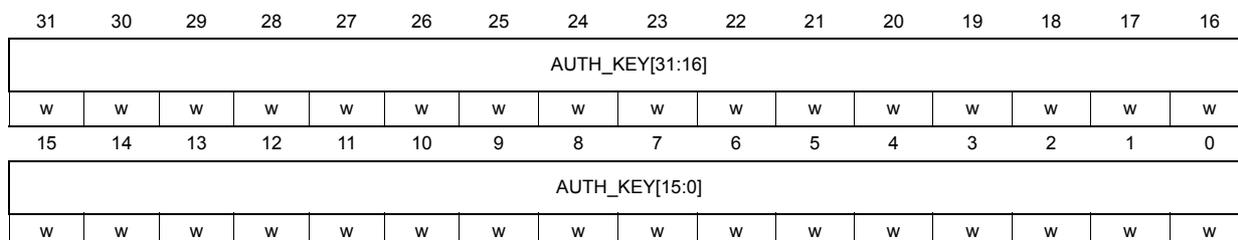
| 31 | 30 | 29 | 28 | 27 | 26 | 25 | 24 | 23 | 22 | 21 | 20 | 19 | 18 | 17 | 16 |
| AUTH_KEY[31:16] | |||||||||||||||
| w | w | w | w | w | w | w | w | w | w | w | w | w | w | w | w |
| 15 | 14 | 13 | 12 | 11 | 10 | 9 | 8 | 7 | 6 | 5 | 4 | 3 | 2 | 1 | 0 |
| AUTH_KEY[15:0] | |||||||||||||||
| w | w | w | w | w | w | w | w | w | w | w | w | w | w | w | w |
Bits 31:0 AUTH_KEY[31:0] : Device authentication key
The device specific 64-bit authentication key (OEMn key) must be written to this register (in two successive 32-bit writes, least significant word first) to permit RDP regression. Writing a wrong key locks access to the device and prevent code execution from the Flash memory.
DBGMCU debug device authentication register (DBGMCU_DBG_AUTH_DEVICE)
Address offset: 0x104
Reset value: 0xXXXX XXXX
| 31 | 30 | 29 | 28 | 27 | 26 | 25 | 24 | 23 | 22 | 21 | 20 | 19 | 18 | 17 | 16 |
|---|---|---|---|---|---|---|---|---|---|---|---|---|---|---|---|
| AUTH_ID[31:16] | |||||||||||||||
| r | r | r | r | r | r | r | r | r | r | r | r | r | r | r | r |
| 15 | 14 | 13 | 12 | 11 | 10 | 9 | 8 | 7 | 6 | 5 | 4 | 3 | 2 | 1 | 0 |
| AUTH_ID[15:0] | |||||||||||||||
| r | r | r | r | r | r | r | r | r | r | r | r | r | r | r | r |
Bits 31:0 AUTH_ID[31:0] : Device specific ID
Device specific ID used for RDP regression.
DBGMCU part number codification register (DBGMCU_PNCR)
Address offset: 0x7DC
Reset value: 0xXXXX XXXX
| 31 | 30 | 29 | 28 | 27 | 26 | 25 | 24 | 23 | 22 | 21 | 20 | 19 | 18 | 17 | 16 |
|---|---|---|---|---|---|---|---|---|---|---|---|---|---|---|---|
| CODIFICATION[31:16] | |||||||||||||||
| r | r | r | r | r | r | r | r | r | r | r | r | r | r | r | r |
| 15 | 14 | 13 | 12 | 11 | 10 | 9 | 8 | 7 | 6 | 5 | 4 | 3 | 2 | 1 | 0 |
| CODIFICATION[15:0] | |||||||||||||||
| r | r | r | r | r | r | r | r | r | r | r | r | r | r | r | r |
Bits 31:0 CODIFICATION[31:0] : Part number codification
0x0032 3541: STMicroelectronics STM32WBA52xx part number codification.
0x0034 3541: STMicroelectronics STM32WBA54xx part number codification.
0x0035 3541: STMicroelectronics STM32WBA55xx part number codification.
DBGMCU CoreSight peripheral identity register 4 (DBGMCU_PIDR4)
Address offset: 0xFD0
Reset value: 0x0000 0000
| 31 | 30 | 29 | 28 | 27 | 26 | 25 | 24 | 23 | 22 | 21 | 20 | 19 | 18 | 17 | 16 |
|---|---|---|---|---|---|---|---|---|---|---|---|---|---|---|---|
| Res. | Res. | Res. | Res. | Res. | Res. | Res. | Res. | Res. | Res. | Res. | Res. | Res. | Res. | Res. | Res. |
| 15 | 14 | 13 | 12 | 11 | 10 | 9 | 8 | 7 | 6 | 5 | 4 | 3 | 2 | 1 | 0 |
| Res. | Res. | Res. | Res. | Res. | Res. | Res. | Res. | F4KCOUNT[3:0] | JEP106CON[3:0] | ||||||
| r | r | r | r | r | r | r | r | ||||||||
Bits 31:8 Reserved, must be kept at reset value.
Bits 7:4 F4KCOUNT[3:0] : Register file size
0x0: The register file occupies a single 4-Kbyte region
Bits 3:0 JEP106CON[3:0] : JEP106 continuation code
0x0: STMicroelectronics JEDEC code
DBGMCU CoreSight peripheral identity register 0 (DBGMCU_PIDR0)
Address offset: 0xFE0
Reset value: 0x0000 0000
| 31 | 30 | 29 | 28 | 27 | 26 | 25 | 24 | 23 | 22 | 21 | 20 | 19 | 18 | 17 | 16 |
|---|---|---|---|---|---|---|---|---|---|---|---|---|---|---|---|
| Res. | Res. | Res. | Res. | Res. | Res. | Res. | Res. | Res. | Res. | Res. | Res. | Res. | Res. | Res. | Res. |
| 15 | 14 | 13 | 12 | 11 | 10 | 9 | 8 | 7 | 6 | 5 | 4 | 3 | 2 | 1 | 0 |
| Res. | Res. | Res. | Res. | Res. | Res. | Res. | Res. | PARTNUM[7:0] | |||||||
| r | r | r | r | r | r | r | r | ||||||||
Bits 31:8 Reserved, must be kept at reset value.
Bits 7:0 PARTNUM[7:0] : Part number bits [7:0]
0x00: DBGMCU part number
DBGMCU CoreSight peripheral identity register 1 (DBGMCU_PIDR1)
Address offset: 0xFE4
Reset value: 0x0000 0000
| 31 | 30 | 29 | 28 | 27 | 26 | 25 | 24 | 23 | 22 | 21 | 20 | 19 | 18 | 17 | 16 |
|---|---|---|---|---|---|---|---|---|---|---|---|---|---|---|---|
| Res. | Res. | Res. | Res. | Res. | Res. | Res. | Res. | Res. | Res. | Res. | Res. | Res. | Res. | Res. | Res. |
| 15 | 14 | 13 | 12 | 11 | 10 | 9 | 8 | 7 | 6 | 5 | 4 | 3 | 2 | 1 | 0 |
| Res. | Res. | Res. | Res. | Res. | Res. | Res. | Res. | JEP106ID[3:0] | PARTNUM[11:8] | ||||||
| r | r | r | r | r | r | r | r | ||||||||
Bits 31:8 Reserved, must be kept at reset value.
Bits 7:4 JEP106ID[3:0] : JEP106 identity code bits [3:0]
0x0: STMicroelectronics JEDEC code
Bits 3:0 PARTNUM[11:8] : Part number bits [11:8]
0x0: DBGMCU part number
DBGMCU CoreSight peripheral identity register 2 (DBGMCU_PIDR2)
Address offset: 0xFE8
Reset value: 0x0000 000A
| 31 | 30 | 29 | 28 | 27 | 26 | 25 | 24 | 23 | 22 | 21 | 20 | 19 | 18 | 17 | 16 |
|---|---|---|---|---|---|---|---|---|---|---|---|---|---|---|---|
| Res. | Res. | Res. | Res. | Res. | Res. | Res. | Res. | Res. | Res. | Res. | Res. | Res. | Res. | Res. | Res. |
| 15 | 14 | 13 | 12 | 11 | 10 | 9 | 8 | 7 | 6 | 5 | 4 | 3 | 2 | 1 | 0 |
| Res. | Res. | Res. | Res. | Res. | Res. | Res. | Res. | REVISION[3:0] | JEDEC | JEP106ID[6:4] | |||||
| r | r | r | r | r | r | r | r | ||||||||
Bits 31:8 Reserved, must be kept at reset value.
Bits 7:4 REVISION[3:0] : Component revision number
0x0: r0p0
Bit 3 JEDEC : JEDEC assigned value
0x1: Designer identifier specified by JEDEC
Bits 2:0 JEP106ID[6:4] : JEP106 identity code bits [6:4]
0x2: STMicroelectronics JEDEC code
DBGMCU CoreSight peripheral identity register 3 (DBGMCU_PIDR3)
Address offset: 0xFEC
Reset value: 0x0000 0000
| 31 | 30 | 29 | 28 | 27 | 26 | 25 | 24 | 23 | 22 | 21 | 20 | 19 | 18 | 17 | 16 |
|---|---|---|---|---|---|---|---|---|---|---|---|---|---|---|---|
| Res. | Res. | Res. | Res. | Res. | Res. | Res. | Res. | Res. | Res. | Res. | Res. | Res. | Res. | Res. | Res. |
| 15 | 14 | 13 | 12 | 11 | 10 | 9 | 8 | 7 | 6 | 5 | 4 | 3 | 2 | 1 | 0 |
| Res. | Res. | Res. | Res. | Res. | Res. | Res. | Res. | REVAND[3:0] | CMOD[3:0] | ||||||
| r | r | r | r | r | r | r | r | ||||||||
Bits 31:8 Reserved, must be kept at reset value.
Bits 7:4 REVAND[3:0] : Metal fix version
0x0: No metal fix
Bits 3:0 CMOD[3:0] : Customer modified
0x0: No customer modifications
DBGMCU CoreSight component identity register 0 (DBGMCU_CIDR0)Address offset: 0xFF0
Reset value: 0x0000 000D
| 31 | 30 | 29 | 28 | 27 | 26 | 25 | 24 | 23 | 22 | 21 | 20 | 19 | 18 | 17 | 16 |
|---|---|---|---|---|---|---|---|---|---|---|---|---|---|---|---|
| Res. | Res. | Res. | Res. | Res. | Res. | Res. | Res. | Res. | Res. | Res. | Res. | Res. | Res. | Res. | Res. |
| 15 | 14 | 13 | 12 | 11 | 10 | 9 | 8 | 7 | 6 | 5 | 4 | 3 | 2 | 1 | 0 |
| Res. | Res. | Res. | Res. | Res. | Res. | Res. | Res. | PREAMBLE[7:0] | |||||||
| r | r | r | r | r | r | r | r | ||||||||
Bits 31:8 Reserved, must be kept at reset value.
Bits 7:0 PREAMBLE[7:0] : Component ID bits [7:0]0x0D: Common ID value
DBGMCU CoreSight peripheral identity register 1 (DBGMCU_CIDR1)Address offset: 0xFF4
Reset value: 0x0000 00F0
| 31 | 30 | 29 | 28 | 27 | 26 | 25 | 24 | 23 | 22 | 21 | 20 | 19 | 18 | 17 | 16 |
|---|---|---|---|---|---|---|---|---|---|---|---|---|---|---|---|
| Res. | Res. | Res. | Res. | Res. | Res. | Res. | Res. | Res. | Res. | Res. | Res. | Res. | Res. | Res. | Res. |
| 15 | 14 | 13 | 12 | 11 | 10 | 9 | 8 | 7 | 6 | 5 | 4 | 3 | 2 | 1 | 0 |
| Res. | Res. | Res. | Res. | Res. | Res. | Res. | Res. | CLASS[3:0] | PREAMBLE[11:8] | ||||||
| r | r | r | r | r | r | r | r | ||||||||
Bits 31:8 Reserved, must be kept at reset value.
Bits 7:4 CLASS[3:0] : Component ID bits [15:12] - component class0xF: no CoreSight component
Bits 3:0 PREAMBLE[11:8] : Component ID bits [11:8]0x0: common ID value
DBGMCU CoreSight component identity register 2 (DBGMCU_CIDR2)
Address offset: 0xFF8
Reset value: 0x0000 0005
| 31 | 30 | 29 | 28 | 27 | 26 | 25 | 24 | 23 | 22 | 21 | 20 | 19 | 18 | 17 | 16 |
|---|---|---|---|---|---|---|---|---|---|---|---|---|---|---|---|
| Res. | Res. | Res. | Res. | Res. | Res. | Res. | Res. | Res. | Res. | Res. | Res. | Res. | Res. | Res. | Res. |
| 15 | 14 | 13 | 12 | 11 | 10 | 9 | 8 | 7 | 6 | 5 | 4 | 3 | 2 | 1 | 0 |
| Res. | Res. | Res. | Res. | Res. | Res. | Res. | Res. | PREAMBLE[19:12] | |||||||
| r | r | r | r | r | r | r | r | ||||||||
Bits 31:8 Reserved, must be kept at reset value.
Bits 7:0 PREAMBLE[19:12] : Component ID bits [23:16]
0x05: Common ID value
DBGMCU CoreSight component identity register 3 (DBGMCU_CIDR3)
Address offset: 0xFFC
Reset value: 0x0000 00B1
| 31 | 30 | 29 | 28 | 27 | 26 | 25 | 24 | 23 | 22 | 21 | 20 | 19 | 18 | 17 | 16 |
|---|---|---|---|---|---|---|---|---|---|---|---|---|---|---|---|
| Res. | Res. | Res. | Res. | Res. | Res. | Res. | Res. | Res. | Res. | Res. | Res. | Res. | Res. | Res. | Res. |
| 15 | 14 | 13 | 12 | 11 | 10 | 9 | 8 | 7 | 6 | 5 | 4 | 3 | 2 | 1 | 0 |
| Res. | Res. | Res. | Res. | Res. | Res. | Res. | Res. | PREAMBLE[27:20] | |||||||
| r | r | r | r | r | r | r | r | ||||||||
Bits 31:8 Reserved, must be kept at reset value.
Bits 7:0 PREAMBLE[27:20] : Component ID bits [31:24]
0xB1: Common ID value
43.12.8 DBGMCU register map and reset values
Table 441. DBGMCU register map and reset values
| Offset | Register name | 31 | 30 | 29 | 28 | 27 | 26 | 25 | 24 | 23 | 22 | 21 | 20 | 19 | 18 | 17 | 16 | 15 | 14 | 13 | 12 | 11 | 10 | 9 | 8 | 7 | 6 | 5 | 4 | 3 | 2 | 1 | 0 |
|---|---|---|---|---|---|---|---|---|---|---|---|---|---|---|---|---|---|---|---|---|---|---|---|---|---|---|---|---|---|---|---|---|---|
| 0x000 | DBGMCU_IDCODE | REV_ID[15:0] | Res. | DEV_ID[11:0] | |||||||||||||||||||||||||||||
| Reset value | X | X | X | X | X | X | X | X | X | X | X | X | X | X | X | X | 0 | 1 | 0 | 0 | 1 | 0 | 0 | 1 | 0 | 0 | 1 | 0 | |||||
| 0x004 | DBGMCU_SCR | Res. | Res. | Res. | Res. | Res. | Res. | CDS | CS | Res. | Res. | Res. | SBF | STOPF | LPMS[2:0] | Res. | Res. | Res. | Res. | Res. | Res. | Res. | Res. | Res. | Res. | Res. | Res. | Res. | DBG_STANDBY | DBG_STOP | Res. | ||
| Reset value | 0 | 0 | 0 | 0 | 0 | 0 | 0 | 0 | 0 | ||||||||||||||||||||||||
| 0x008 | DBGMCU_APB1LFZR | Res. | Res. | Res. | Res. | Res. | Res. | Res. | Res. | Res. | Res. | DBG_I2C1_STOP | Res. | Res. | Res. | Res. | Res. | Res. | Res. | Res. | DBG_IWDG_STOP | DBG_WWDG_STOP | Res. | Res. | Res. | Res. | Res. | Res. | Res. | Res. | Res. | DBG_TIM3_STOP | DBG_TIM2_STOP |
| Reset value | 0 | 0 | 0 | 0 | 0 | ||||||||||||||||||||||||||||
| 0x00C | DBGMCU_APB1HFZR | Res. | Res. | Res. | Res. | Res. | Res. | Res. | Res. | Res. | Res. | Res. | Res. | Res. | Res. | Res. | Res. | Res. | Res. | Res. | Res. | Res. | Res. | Res. | Res. | Res. | Res. | DBG_LPTIM2_STOP | Res. | Res. | Res. | Res. | Res. |
| Reset value | 0 | ||||||||||||||||||||||||||||||||
| 0x010 | DBGMCU_APB2FZR | Res. | Res. | Res. | Res. | Res. | Res. | Res. | Res. | Res. | Res. | Res. | Res. | DBG_TIM17_STOP | DBG_TIM16_STOP | Res. | Res. | Res. | Res. | Res. | Res. | DBG_TIM1_STOP | Res. | Res. | Res. | Res. | Res. | Res. | Res. | Res. | Res. | Res. | Res. |
| Reset value | 0 | 0 | 0 | ||||||||||||||||||||||||||||||
| 0x014 to 0x020 | Reserved | Reserved | |||||||||||||||||||||||||||||||
| 0x024 | DBGMCU_APB7FZR | Res. | DBG_RTC_STOP | Res. | Res. | Res. | Res. | Res. | Res. | Res. | Res. | Res. | Res. | Res. | DBG_LPTIM1_STOP | Res. | Res. | Res. | Res. | Res. | Res. | Res. | DBG_I2C3_STOP | Res. | Res. | Res. | Res. | Res. | Res. | Res. | Res. | Res. | Res. |
| Reset value | 0 | 0 | 0 | ||||||||||||||||||||||||||||||
| 0x028 | DBGMCU_AHB1FZR | Res. | Res. | Res. | Res. | Res. | Res. | Res. | Res. | Res. | Res. | Res. | Res. | Res. | Res. | Res. | Res. | Res. | Res. | Res. | Res. | Res. | Res. | Res. | DBG_GPDMA1_CH7_STOP | DBG_GPDMA1_CH6_STOP | DBG_GPDMA1_CH5_STOP | DBG_GPDMA1_CH4_STOP | DBG_GPDMA1_CH3_STOP | DBG_GPDMA1_CH2_STOP | DBG_GPDMA1_CH1_STOP | DBG_GPDMA1_CH0_STOP | Res. |
| Reset value | 0 | 0 | 0 | 0 | 0 | 0 | 0 | 0 | |||||||||||||||||||||||||
Table 441. DBGMCU register map and reset values (continued)
| Offset | Register name | 31 | 30 | 29 | 28 | 27 | 26 | 25 | 24 | 23 | 22 | 21 | 20 | 19 | 18 | 17 | 16 | 15 | 14 | 13 | 12 | 11 | 10 | 9 | 8 | 7 | 6 | 5 | 4 | 3 | 2 | 1 | 0 | |
|---|---|---|---|---|---|---|---|---|---|---|---|---|---|---|---|---|---|---|---|---|---|---|---|---|---|---|---|---|---|---|---|---|---|---|
| 0x02C to 0x0F8 | Reserved | Reserved | ||||||||||||||||||||||||||||||||
| 0x0FC | DBGMCU_SR | AP_ENABLED[15:0] | ||||||||||||||||||||||||||||||||
| Reset value | 0 | 0 | 0 | 0 | 0 | 0 | 0 | 0 | 0 | 0 | 0 | 0 | 0 | 0 | X | X | 0 | 0 | 0 | 0 | 0 | 0 | 0 | 0 | 0 | 0 | 0 | 0 | 0 | 0 | 0 | 1 | 1 | |
| 0x100 | DBGMCU_DBG_AUTH_HOST | AUTH_KEY[31:0] | ||||||||||||||||||||||||||||||||
| Reset value | X | X | X | X | X | X | X | X | X | X | X | X | X | X | X | X | X | X | X | X | X | X | X | X | X | X | X | X | X | X | X | X | ||
| 0x104 | DBGMCU_DBG_AUTH_DEVICE | AUTH_KEY[31:0] | ||||||||||||||||||||||||||||||||
| Reset value | X | X | X | X | X | X | X | X | X | X | X | X | X | X | X | X | X | X | X | X | X | X | X | X | X | X | X | X | X | X | X | X | ||
| 0x108 to 0x7D8 | Reserved | Reserved | ||||||||||||||||||||||||||||||||
| 0x7DC | DBGMCU_PNCR | CODIFICATION[31:0] | ||||||||||||||||||||||||||||||||
| Reset value | X | X | X | X | X | X | X | X | X | X | X | X | X | X | X | X | X | X | X | X | X | X | X | X | X | X | X | X | X | X | X | X | ||
| 0x7E0 to 0xFCC | Reserved | Reserved | ||||||||||||||||||||||||||||||||
| 0xFD0 | DBGMCU_PIDR4 | Res | Res | Res | Res | Res | Res | Res | Res | Res | Res | Res | Res | Res | Res | Res | Res | Res | Res | Res | Res | Res | Res | Res | Res | Res | Res | Res | Res | Res | Res | Res | Res | Res |
| Reset value | ||||||||||||||||||||||||||||||||||
| 0xFD4 to 0xFDC | Reserved | Reserved | ||||||||||||||||||||||||||||||||
| 0xFE0 | DBGMCU_PIDR0 | Res | Res | Res | Res | Res | Res | Res | Res | Res | Res | Res | Res | Res | Res | Res | Res | Res | Res | Res | Res | Res | Res | Res | Res | Res | Res | Res | Res | Res | Res | Res | Res | |
| Reset value | ||||||||||||||||||||||||||||||||||
| 0xFE4 | DBGMCU_PIDR1 | Res | Res | Res | Res | Res | Res | Res | Res | Res | Res | Res | Res | Res | Res | Res | Res | Res | Res | Res | Res | Res | Res | Res | Res | Res | Res | Res | Res | Res | Res | Res | Res | |
| Reset value | ||||||||||||||||||||||||||||||||||
| 0xFE8 | DBGMCU_PIDR2 | Res | Res | Res | Res | Res | Res | Res | Res | Res | Res | Res | Res | Res | Res | Res | Res | Res | Res | Res | Res | Res | Res | Res | Res | Res | Res | Res | Res | Res | Res | Res | Res | |
| Reset value | ||||||||||||||||||||||||||||||||||
| 0xFEC | DBGMCU_PIDR3 | Res | Res | Res | Res | Res | Res | Res | Res | Res | Res | Res | Res | Res | Res | Res | Res | Res | Res | Res | Res | Res | Res | Res | Res | Res | Res | Res | Res | Res | Res | Res | Res | |
| Reset value | ||||||||||||||||||||||||||||||||||
| 0xFF0 | DBGMCU_CIDR0 | Res | Res | Res | Res | Res | Res | Res | Res | Res | Res | Res | Res | Res | Res | Res | Res | Res | Res | Res | Res | Res | Res | Res | Res | Res | Res | Res | Res | Res | Res | Res | Res | |
| Reset value | ||||||||||||||||||||||||||||||||||
| 0xFF4 | DBGMCU_CIDR1 | Res | Res | Res | Res | Res | Res | Res | Res | Res | Res | Res | Res | Res | Res | Res | Res | Res | Res | Res | Res | Res | Res | Res | Res | Res | Res | Res | Res | Res | Res | Res | Res | |
| Reset value | ||||||||||||||||||||||||||||||||||
| 0xFF8 | DBGMCU_CIDR2 | Res | Res | Res | Res | Res | Res | Res | Res | Res | Res | Res | Res | Res | Res | Res | Res | Res | Res | Res | Res | Res | Res | Res | Res | Res | Res | Res | Res | Res | Res | Res | Res | |
| Reset value | ||||||||||||||||||||||||||||||||||
| 0xFFC | DBGMCU_CIDR3 | Res | Res | Res | Res | Res | Res | Res | Res | Res | Res | Res | Res | Res | Res | Res | Res | Res | Res | Res | Res | Res | Res | Res | Res | Res | Res | Res | Res | Res | Res | Res | Res | |
| Reset value | ||||||||||||||||||||||||||||||||||
Refer to Section 43.5.1: System debug ROM table and Section 43.6.1: CPU ROM tables for the register boundary addresses.
43.13 References
- 1. IHI 0031C (ID080813) - Arm ® Debug Interface Architecture Specification ADIv5.0 to ADIv5.2, Issue C, 8th Aug 2013
- 2. DDI 0480F (ID100313) - Arm ® CoreSight ™ SoC-400 r3p2 Technical Reference Manual, Issue G, 16th March 2015
- 3. DDI 0314H - Arm ® CoreSight ™ Components Technical Reference Manual, Issue H, 10 July, 2009
- 4. DDI 0553A (ID092917) - Arm ® v8-M Architecture Reference Manual, Issue A.f, 29 September 2017
- 5. 100230_0002_00_en - Arm ® Cortex ® -M33 Processor r0p2 Technical Reference Manual, Issue 0002-00, 10 May 2017