9. Radio system
9.1 Introduction
The 2.4 GHz RADIO is ultra-low power, operating in the 2.4 GHz ISM band. It provides Bluetooth® LE 1 Mbps coded, 1 Mbps, and 2 Mbps non-coded GFSK, and IEEE802.15.4 chip rate 2 Mchip/s, spreading mode DSSS, data rate 125 and 250 kbps O-QPSK-C modulation.
The 2.4 GHz RADIO is compliant with the Bluetooth® LE, Thread, and Zigbee® specifications, and radio regulations including ETSI EN 300 328, EN 300 440, EN 301 489-17, ARIB STD-T66, FCC CFR47 part 15 section 15.205, 15.209, 15.247, and 15.249, IC RSS-139, and RSS-210.
9.2 Main features
- • Radio protocol:
- – Bluetooth® LE
- – IEEE802.15.4
- – Proprietary protocols
- – Concurrent mode
- • Bluetooth® LE features:
- – PHY support: 1 Mbps uncoded, 500 kbps and 125 kbps coded, 2 Mbps
- – Device privacy and network privacy modes
- – Anonymous device address types
- – Advertising extension PDUs
- – Advertising channel index
- – Periodic advertising synchronous transfer
- – High duty cycle, nonconnectable advertising
- – Channel selection algorithm #2
- – Angle of arrival (AoA), angle of departure (AoD)
- – Up to 20 connections in any role in addition to advertiser and scanner roles
- – Audio connected isochronous streams
- – Audio broadcast isochronous streams
- • IEEE 802.15.4 features:
- – Beacon management
- – 16-bit short and 64-bit IEEE addressing modes
- – PAN formation along with association and disassociation
- – Full handshake protocol for transfer reliability, frame validation, and acknowledgment frame delivery
- – IEEE802.15.4 2020 MAC for non-beaconed PANs
- • External PA
- • Packet traffic arbitration
9.3 2.4 GHz RADIO implementation
Table 75. 2.4 GHz RADIO implementation
| Feature (1) | STM32WBA55xx | STM32WBA54xx | STM32WBA52xx | STM32WBA50xx |
|---|---|---|---|---|
| Bluetooth® LE AoA/AoD | X | X | - | - |
| External PA | X | X | - | - |
| Packet traffic arbitration | X | X | - | - |
| IEEE802.15.4 | X | X | - | - |
1. X = supported
9.4 Functional description
9.4.1 Block diagram
Figure 21. Radio system block diagram
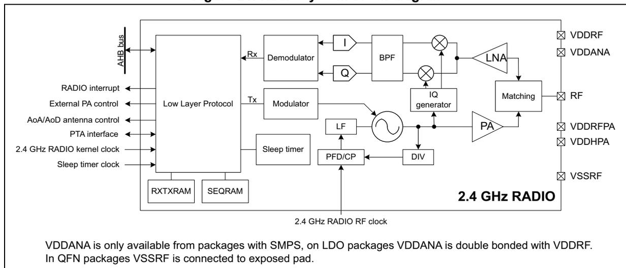
VDDANA is only available from packages with SMPS, on LDO packages VDDANA is double bonded with VDDRF.
In QFN packages VSSRF is connected to exposed pad.
Note: Bluetooth® LE AoA/AoD, external PA control, and PTA interface are available only on STM32WBA54/55xx devices. VDDANA and VSSRF are available only on STM32WBA55xx devices.
9.4.2 Pins and internal signals
Table 76. Input / output pins
| Pin name | Signal type | Description |
|---|---|---|
| RF | RF | 2.4 GHz RF input output |
| RADIO interrupt | Output | 2.4 GHz RADIO interrupt to the CPU |
| External PA control | Output | External PA control |
Table 76. Input / output pins (continued)
| Pin name | Signal type | Description |
|---|---|---|
| AoA/AoD antenna control | Output | Angle of arrival/departure antenna area control |
| PTA interface | Input/Output | Packet traffic arbitration control |
9.4.3 Transmit output power
The 2.4 GHz RADIO includes an internal PA. The transmit output power can be increased using an additional external PA. External PA control signals BYPASS can be selected on GPIOs (see the datasheet), and the signal ENABLE can be mapped on any free GPIO by application software.
Figure 22 shows the transmit path and output power control.
Figure 22. Transmit path and output power control
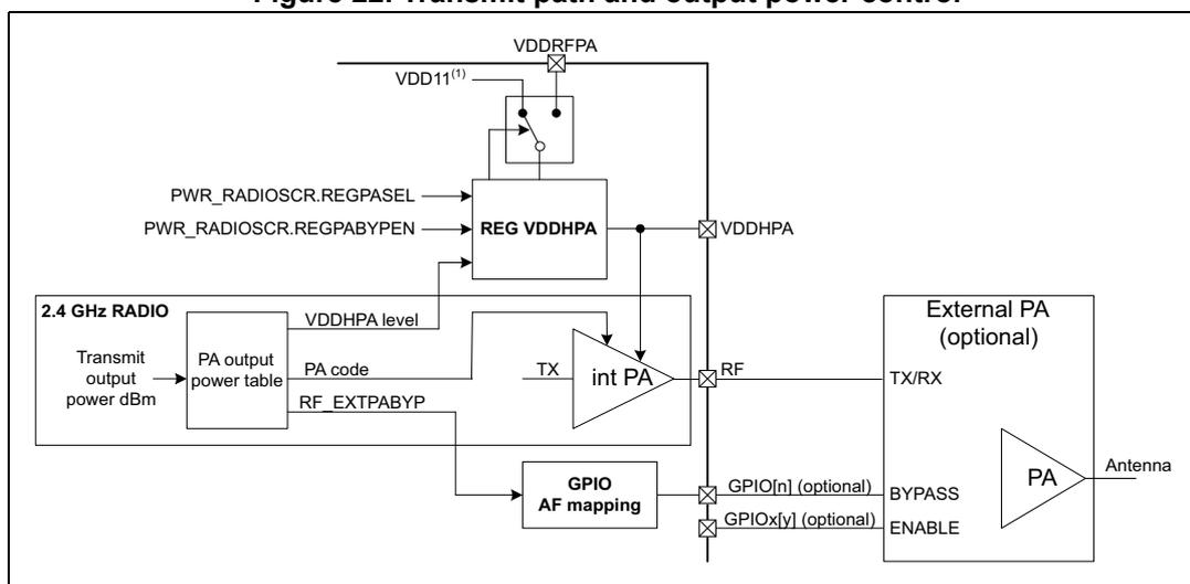
1. VDD11 must be selected only when supplied from device SMPS.
The transmit output power (in dBm) is dependent upon the V DDHPA voltage level and the PA code, and, when the application supports an external PA, an external PA bypass indication. The values for these parameters are defined in a PA output power table available to the link layer software.
Table 77. PA output power table format
| V DDHPA level | PA code | BYPASS |
|---|---|---|
| 0x0 = 0.90 V | ||
| 0x1 = 0.95 V | ||
| 0x2 = 1.0 V | ||
| 0x3 = 1.1 V | 0 to 25 dec. | 0 or 1 |
| ... | ||
| 0xE = 2.2 V | ||
| 0xF = 2.3 V |
The internal PA maximum transmit output power is depended upon the \( V_{DDHPA} \) voltage level and the PA code. The maximum \( V_{DDHPA} \) voltage level is dependent upon the application ( \( V_{DDRFPA} \) pin) supply scheme, see Table 78 for details.
The REGPASEL and REGPABYPEN allow the REG \( V_{DDHPA} \) regulator input voltage to be controlled.
Table 78. 2.4 GHz RADIO supply configuration
| \( V_{DDHPA} \) level | Minimum \( V_{DDRFPA} \) | Internal PA max transmit output power |
|---|---|---|
| 1.0 V | 1.2 V (1) | + 3 dBm |
| 1.2 V | 1.71 V | + 6 dBm |
| 1.5 V | 1.8 V | + 8 dBm |
| 2.3 V | 2.6 V | + 10 dBm |
1. Only on STM32WBA55xx devices when SMPS is used.
9.4.4 Bluetooth® LE AoA and AoD
Up to eight antennas are supported by means of the coded \( RF\_ANTSW[2:0] \) signal bus available through GPIO alternate function for Bluetooth® LE AoA when receiving the constant tone extension of a packet, or for AoD while transmitting the constant tone extension of a packet.
Figure 23. Bluetooth® LE AoA/AoD antennas control
![Figure 23: Bluetooth® LE AoA/AoD antennas control diagram. The diagram shows the internal architecture of the 2.4 GHz RADIO. It includes a TX path with an internal PA (int PA) and a Matching block, and an RX path with an LNA. The RF output is connected to an Antenna matrix (optional) via a TX/RX switch. The Antenna matrix is controlled by a Control block with inputs V1, V2, and V3. The Control block is connected to GPIOs (GPIOx, GPIOy, GPIOz) via an AF mapping block. The RF_ANTSW[2:0] signal bus is also connected to the AF mapping block. The Antenna matrix outputs are labeled Antenna1 through Antenna8.](/RM0493-STM32WBA5/d160ca77eef02560657f6218a3d2017f_img.jpg)
9.4.5 RXTX data SRAM access
The Link Layer software must put the 2.4 GHz RADIO in Sleep mode to let the host application access the 2.4 GHz RADIO RXTXRAM. When the access is no longer needed, the host application must request the Link Layer software to put the 2.4 GHz RADIO in DeepSleep mode.
To access the RXTX data SRAM, both the 2.4 GHz RADIO bus clock and the kernel clock must be active and ready.
The 2.4 GHz RADIO modes depend upon the host application request, and upon the Link Layer scheduled radio activity.
9.5 Low-power modes
The 2.4 GHz RADIO supports autonomous operation down to Stop 0 mode voltage scaling range 1, and the 2.4 GHz RADIO sleep timer remains operational down to Standby retention mode.
The 2.4 GHz RADIO in autonomous mode is able to transmit and receive packets over the air for the radio connection.
The 2.4 GHz RADIO sleep timer allows to maintain radio connections when the radio is in low power mode, for example between Bluetooth® LE connection events.
Table 79. Effect of low-power modes on the 2.4 GHz RADIO
| Mode | Description |
|---|---|
| Sleep | No effect. 2.4 GHz RADIO and 2.4 GHz RADIO sleep timer interrupts cause the device to exit Sleep mode. Radio connection are maintained. |
| Stop 0 voltage range 1 | The 2.4 GHz RADIO will autonomously transmit and receive packets, 2.4 GHz RADIO and 2.4 GHz RADIO sleep timer interrupts cause the device to exit Stop 0 mode. Radio connections are maintained. |
| Stop 0 voltage range 2 and Stop 1 | The 2.4 GHz RADIO full configuration is retained but is no longer capable to transmit and receive packets, The 2.4 GHz RADIO sleep timer interrupt cause the device to exit Stop mode. Radio connections are maintained during Bluetooth® LE connection intervals. |
| Standby retention | The 2.4 GHz RADIO is powered down. The minimum configuration information is retained even if it is no longer capable to transmit and receive packets, The 2.4 GHz RADIO sleep timer interrupt cause the device to exit Stop mode. Radio connections are maintained during Bluetooth® LE connection intervals. |
| Standby | The 2.4 GHz RADIO and 2.4 GHz RADIO sleep timer are powered down. Radio connections are lost. |