8. Instruction cache (ICACHE)
8.1 ICACHE introduction
The instruction cache (ICACHE) is introduced on the C-AHB code bus of the Cortex ® -M33 processor, to improve performance when fetching instructions and data from internal memories.
Some specific features, like dual master ports, hit-under-miss, and critical-word-first refill policy, result in close to zero-wait-state performance in most use cases.
8.2 ICACHE main features
The main features of ICACHE are listed below:
- • Bus interface
- – One 32-bit AHB slave port, the execution port (input from Cortex ® -M33 C-AHB code interface)
- – Two AHB master ports: master1 and master2 ports, with outputs to Fast and Slow buses of main AHB bus matrix, respectively
- – One 32-bit AHB slave port for control (input from AHB peripherals interconnect, for ICACHE registers access)
- • Cache access
- – 0 wait-state on hits
- – Hit-under-miss capability: ability to serve processor requests (access to cached data) during an ongoing line refill due to a previous cache miss
- – Dual master access: feature used to decouple the traffic according to targeted memory. For example, the ICACHE assigns fast traffic (addressing flash memories) to the AHB master1 port, and slow traffic (addressing SRAMs) to the AHB master2 port, thus preventing processor stalls on line refills from SRAMs. This allows ISR (interrupt service routine) fetching on internal flash memory to take place in parallel with a cache line refill from SRAMs.
- – Minimal impact on interrupt latency, thanks to dual master
- – Optimal cache line refill thanks to WRAPw bursts of the size of the cache line (32-bit word size, w , aligned on cache line size)
- – n-way set-associative default configuration with possibility to configure as 1-way, means direct mapped cache, for applications needing very-low-power consumption profile
- • Memory address remap
- – Possibility to remap input address falling into up to four memory regions (used to remap aliased code in SRAM memories to the code region, for execution from the C-AHB code interface)
- • Replacement and refill
- – pLRU-t (pseudo-least-recently-used, based on binary tree) replacement policy, algorithm with best complexity/performance balance
- – Critical-word-first refill policy, minimizing processor stalls
- – Possibility to configure burst type of AHB memory transaction for remapped regions: INCRw or WRAPw (size w aligned on cache line size)
- • Performance counters
The ICACHE implements two performance counters:- – Hit monitor counter (32-bit)
- – Miss monitor counter (16-bit)
- • Error management
- – Possibility to detect an unexpected cacheable write access, to flag an error, and optionally, to raise an interrupt
- • TrustZone® security support
- • Maintenance operation
- – Cache invalidate: full cache invalidation, fast command, noninterruptible
8.3 ICACHE implementation
Table 67. ICACHE features
| Feature | ICACHE |
|---|---|
| Number of ways | 2 |
| Cache size | 8 Kbytes |
| Cache line width | 16 bytes |
| Range granularity of memory regions to be remapped | 2 Mbytes |
| Number of regions to remap | 4 |
| Data size of AHB slave interface | 32 bits |
| Data size of AHB fast master1 interface | 128 bits |
| Data size of AHB slow master2 interface | 32 bits |
8.4 ICACHE functional description
The purpose of this block is to cache instruction fetches or instruction memories loads, coming from the processor. As such, the ICACHE manages only cacheable read transactions, and does not manage cacheable write transactions.
The noncacheable transactions (both read and write) bypass the ICACHE.
For the error management purpose, if a write cacheable transaction is presented (this happens only in case of bad software programming), the ICACHE sets an error flag and, if enabled, raises an interrupt to the processor.
8.4.1 ICACHE block diagram
Figure 18. ICACHE block diagram
8.4.2 ICACHE reset and clocks
The ICACHE is clocked on the Cortex ® -M33 C-AHB bus clock.
When the ICACHE reset signal is released, a cache invalidate procedure is automatically launched, making the ICACHE busy (ICACHE_SR = 0x0000 0001).
When this procedure is finished:
- • the ICACHE is invalidated: “cold cache”, with all cache line valid bits = 0 (ICACHE must be filled up)
- • ICACHE_SR = 0x0000 0002 (reflecting the cache is no longer busy)
- • the ICACHE is disabled: the EN bit in ICACHE_CR holds its reset state (= 0).
Note: When disabled, the ICACHE is bypassed, except the remapping mechanism that is still functional: slave input requests (remapped or not) are forwarded to the master port(s).
8.4.3 ICACHE TAG memory
The ICACHE TAG memory contains:
- • address tags indicating which data are contained in the cache data memories
- • validity bits
There is one valid bit per cache line (per way).
The valid bit is set when a cache line is refilled (after a miss).
Valid bits are reset in any of the below cases:
- • after the ICACHE reset is released
- • when the cache is disabled, by setting EN = 0 in ICACHE_CR (by software)
- • when executing an ICACHE invalidate command, by setting CACHEINV = 1 in ICACHE_CR (by software)
When a cacheable transaction is received at the execution input port, its AHB address (HADDR_in) is split into the following fields (see Table 68 for B and W definitions):
- • HADDR_in[B-1:0]: address byte offset, indicates which byte to select inside a cache line.
- • HADDR_in[B+W-1:B]: address way index, indicates which cache line to select inside each way.
- • HADDR_in[31:B+W]: tag address, to be compared to the TAG memory address to check if the requested data is already available (meaning valid) inside the ICACHE.
The following table gives a summary of the ICACHE main parameters for TAG memory dimensioning. Figure 19 shows the functional view of TAG and data memories, for an n-way set associative ICACHE.
Table 68. TAG memory dimensioning parameters for n-way set associative operating mode (default)
| Parameter | Value | Example |
|---|---|---|
| Cache size | S Kbytes = s bytes (s = 1024 x S) | 8 Kbytes = 8192 bytes |
| Cache number of ways | n | 2 |
| Cache line size | L-byte = l-bit (l = 8 x L) | 16-byte = 128-bit |
| Number of cache lines | LpW = s / (n x L) lines / way | 256 lines / way |
| Address byte offset size | B = log 2 (L) bit | 4-bit |
| Address way index size | W = log 2 (LpW) bit | 8-bit |
| TAG address size | T = (32 - W - B) bit | 20-bit |
Figure 19. ICACHE TAG and data memories functional view
MSv48192V2
8.4.4 Direct-mapped ICACHE (1-way cache)
The default configuration (at reset) is an n-way set associative cache (WAYSEL = 1 in ICACHE_CR), but the user can configure the ICACHE as direct mapped by writing WAYSEL = 0 (only possible when the cache is disabled, EN = 0 in ICACHE_CR).
The following table gives a summary of ICACHE main parameters for TAG memory when the direct-mapped cache operating mode is selected.
Table 69. TAG memory dimensioning parameters for direct-mapped cache mode
| Parameter | Value | Example |
|---|---|---|
| Cache size | \( S \text{ Kbytes} = s \text{ bytes } (s = 1024 \times S) \) | 8 Kbytes = 8192 bytes |
| Cache number of ways | 1 | 1 |
| Cache line size | \( L\text{-byte} = l\text{-bit } (l = 8 \times L) \) | 16-byte = 128-bit |
| Number of cache lines | \( LpW = s / L \text{ lines} \) | 512 lines |
| Address byte offset size | \( B = \log_2(L) \text{ bit} \) | 4-bit |
| Address way index size | \( W = \log_2(LpW) \text{ bit} \) | 9-bit |
| TAG address size | \( T = (32 - W - B) \text{ bit} \) | 19-bit |
All cache operations (such as read, refill, remapping, invalidation) remain the same in the direct-mapped configuration. The only difference is the absence of a replacement algorithm in case of line eviction (as explained in Section 8.4.8 ): only one way (the unique one) is possible for any data refill.
8.4.5 ICACHE enable
To activate the ICACHE, the EN bit in ICACHE_CR must be set to 1.
When the ICACHE is disabled, it is bypassed and all transactions are copied from the slave to the master ports in the same clock cycle.
It is recommended to initialize or modify the main memory content (region to be later cached) with the ICACHE disabled, and to enable the ICACHE only when this region remains unchanged (an enabled ICACHE detects cacheable write transactions as errors).
To ensure performance determinism, it is recommended to wait for the end of a potential cache invalidate procedure before enabling the ICACHE. This procedure occurs when the hardware reset signal is released, when CACHEINV is set, or when EN is cleared in ICACHE_CR. During the procedure, BUSYF is set in ICACHE_SR, and once finished, BUSYF is cleared and BSYENDF is set in the same register (raising the ICACHE interrupt if enabled on such a busy end condition).
The software must test BUSYF and/or BSYENDF values before enabling the ICACHE. Else, if the ICACHE is enabled before the end of an invalidate procedure, any cache access (while BUSYF = 1) is treated as noncacheable, and its performance depends on the main memory access time.
The address remapping is performed, whether the ICACHE is enabled or not, if the input transaction address falls into the memory regions defined and enabled in ICACHE_CRRx (see Figure 20 ).
The ICACHE is, by default, disabled at boot.
8.4.6 Cacheable and noncacheable traffic
The ICACHE is developed for the Cortex ® -M33 core. It is placed on the C-AHB bus, and thus caches the code memory region, ranging from address 0x0000 0000 to 0x1FFF FFFF of the memory map.
To make other memory regions cacheable, the ICACHE supports a memory region remapping feature, used to define up to four SRAM regions, whose addresses have an alias in the code region. Addressing these memory regions through their code alias address allows the memory request to be routed to the C-AHB bus, and to be managed by the ICACHE.
Any SRAM space physically mapped at an address in range [0x2000 0000:0x3FFF FFFF] can be aliased with an address in range [0x0A00 0000:0x0AFF FFFF] or [0x0E00 0000:0x0EFF FFFF].
For a given memory request in the code region, the ICACHE implements the address remapping functionality first. If aliased, it is the remapped address, which is then cached, and, if needed, provided to the master port to address the main AHB bus matrix. The destination physical address does not need further manipulation on the AHB bus.
The remapping functionality is available also for noncacheable traffic, and when the cache is disabled.
Additional details on address remapping are provided in Section 8.4.7 .
An incoming memory request to the ICACHE is defined as cacheable according to its AHB transaction memory lookup attribute, as shown in Table 70 . This AHB attribute depends on the MPU (memory protection unit) programming for the addressed region.
Table 70. ICACHE cacheability for AHB transaction
| AHB lookup attribute | Cacheability |
|---|---|
| 1 | Cacheable |
| 0 | Noncacheable |
In the case of a noncacheable access (read or write), the ICACHE is bypassed. The AHB transaction is propagated unchanged to the master output port, except the transaction address, which may be modified due to the address remapping feature (see Section 8.4.7 ).
The bypass, and eventual remap logic, does not increase the latency of the access to the targeted memory.
In the case of a cacheable access, the ICACHE behaves as explained in Section 8.4.8 .
Cacheable memory regions are defined and programmed by the user in the MPU responsible for the generation of the AHB attribute signals for any transaction addressing a given region.
Table 71 summarizes programmable configurations of various memories.
Table 71. Memory configurations
| Memory | Cacheable (MPU programming) | Remapped in the ICACHE (ICACHE_CRRx programming) |
|---|---|---|
| Flash | Yes or no | Not required |
| SRAM | Yes (not recommended) | Required |
| No | Required if the user wants code in SRAM fetched on C-AHB bus (else on S-AHB bus) |
8.4.7 Address remapping
The ICACHE allows an alias address to be defined in the code region for up to four SRAM memory regions.
The address remapping is applied on the code alias address, transforming it into the destination SRAM physical address.
The remapping operation is fully software configurable by programming ICACHE_CRRx ( \( x = 0 \) to 3, number of remapped regions). This programming can be done only when the ICACHE is disabled.
Each region \( x \) can be individually enabled with REN in ICACHE_CRRx. Once enabled, the remap operation occurs even if the ICACHE is disabled, or if the transaction is noncacheable.
Remap regions can have different size: each can be programmed in RSIZE of its ICACHE_CRRx. The size of each region is a power of two multiple of range granularity (2 Mbytes), with a minimum of 2 Mbytes, and a maximum of 128 Mbytes.
The address remapping mechanism is based on the matching of an incoming AHB address (HADDR_in) with a given code subregion base-address, and the modification of this address into its (remapped) physical address, as follows:
- • HADDR_in belongs to region x if HADDR_in[31:RI] = 000:BASEADDR[28:RI], where:
- – 000:BASEADDR is the code subregion base-address programmed in BASEADDR of ICACHE_CRRx.
- – RI defines the number of significant bits to consider. RI = \( \log_2 \) (region size) with a minimum value of 21 (for a 2-Mbyte region) and a maximum value of 27 (for a 128-Mbyte region).
- • If the region x is enabled, the master port output AHB address (HADDR_out) is composed by concatenating the two below parts:
- – REMAPADDR[31:RI] field of ICACHE_CRRx as MSBs
- – HADDR_in[RI-1:0] as LSBs
Figure 20 describes the matching and the output address generation.
Figure 20. ICACHE remapping address mechanism
The diagram illustrates the ICACHE remapping address mechanism. At the top, the input address HADDR_in (bits 31 to 0) is shown. A portion of this address, bits 31 to RI-1, is compared with the programmed base address 000:BASEADDR[28:RI] using an equality comparator (==). The output of this comparator, labeled 'Address in region x', controls a 2-to-1 multiplexer. The multiplexer selects between two inputs: '0' (representing the REMAPADDR[31:RI] field) and '1' (representing the HADDR_in[RI-1:0] field). The output of the multiplexer is concatenated with the lower bits of the input address, HADDR_in[RI-1:0], to form the output address HADDR_out (bits 31 to 0). The diagram is labeled MSV48194V2 in the bottom right corner.
Table 72 summarizes all possible configurations of BASEADDR and REMAPADDR sizes (number of significant MSBs) in ICACHE_CRRx, depending upon RSIZE.
Table 72. ICACHE remap region size, base address, and remap address
| Region size (Mbytes) | Base address size (MSBs) | Remap address (MSBs) |
|---|---|---|
| 2 | 8 | 11 |
| 4 | 7 | 10 |
| 8 | 6 | 9 |
| 16 | 5 | 8 |
| 32 | 4 | 7 |
| 64 | 3 | 6 |
| 128 | 2 | 5 |
Care must be taken while programming BASEADDR and REMAPADDR in ICACHE_CRRx: if the programmed value is bigger than expected (number of MSBs, see Table 72), the unneeded extra LSBs are ignored.
and Typical remapping example: a 2-Mbyte SRAM region physically located in the address range [0x2000 0000:0x201F FFFF], remapped in the code section range [0x1000 0000:0x101F FFFF]:
- • REMAPADDR[31:21] = 0x100
- • BASEADDR[28:21] = 0x80
- • HADDR_in[31:21] is compared to 000:BASEADDR[28:21].
If the comparison matches:
- • HADDR_out[31:21] gets REMAPADDR[31:21] (in place of HADDR_in[31:21])
- • HADDR_out[20:0] gets HADDR_in[20:0]
The software can program the kind of AHB burst generated by the ICACHE master ports on the bus matrix (for cache line refill), by setting HBURST in ICACHE_CRRx with:
- • WRAP for remapped SRAMs that can support WRAP burst mode, providing the benefit of the critical-word-first feature performance:
- – WRAP burst size = cache line size
- – WRAP burst start address = word address of the first data requested by the core
Note: Coherency is needed when programming the SAU (secure attribution unit) and the MPU (memory protection unit) attributes for both the SRAMs regions and their aliased code subregions.
8.4.8 Cacheable accesses
When the ICACHE receives a cacheable transaction from the Cortex ® -M33, it checks if the address requested is present in its TAG memory, and if the corresponding cache line is valid.
There are then three alternatives:
- • The address is present inside the TAG memory, the cache line is valid: cache hit , the data is read from the cache and provided to the processor in the same cycle.
- • The address is not present in the TAG memory: cache miss , the data is read from the main memory and provided to the processor, and a cache line refill is performed.
The critical-word-first policy ensures minimum wait cycles for the processor, since read data can be provided while the cache still performs a cache line refill (associated latency is the latency of fetching one word from the main memory).
The burst generated on the ICACHE master bus is WRAP w (w being the cache line width, in words) if no address remap occurs. If an address remap occurs, the kind of burst depends upon the HBURST programmed in corresponding ICACHE_CRRx.
The AHB transaction attributes are also propagated to the main AHB bus matrix on the master port selected for the line refill.
- • The address is not present in TAG memory, but belongs to the refill burst from the main memory currently ongoing: cache hit (hit-under-miss feature).
This happens during cache-line refill. The ICACHE can provide the requested data as soon as data are available at its master interface, thus avoiding a miss (fetching data from the main memory).
In the case of cache refill (due to cache miss), the ICACHE selects which cache line is written with the refill data:
- • In direct map (1-way) mode, only one line can be used to store the refill data: the line pointed by the index of the input address.
- • In n-way set associative mode, one line among n can be used (the line pointed by the address index, in each of the n ways). The way selection is based on a pLRU-t replacement algorithm that points, for each index, on the way candidate for the next refill.
If the cache line where the refill data must be written is already valid, the targeted cache line must be invalidated first. This is true whatever the direct map or n-way set associative cache mode.
8.4.9 Dual-master cache
The ICACHE implements a dual-port AHB master on the main AHB bus matrix: master1 and master2 ports. This is used to split the traffic going to different destination memories.
The nonremapped traffic goes systematically to master1 port. The remapped traffic can be routed on the master2 port by programming MSTSEL in ICACHE_CRRx (on a region basis).
The code can typically be fetched as follows:
- • internal flash memory on master1 port (Fast bus)
- • SRAM on master2 port (Slow bus)
For systems not implementing external memories, the traffic to the internal flash memory can be decoupled from the traffic to the internal SRAM (when remapped by the ICACHE). This feature is used to prevent further processor stalls on misses.
Alongside with hit-under-miss, this dual-master feature allows the processor to have an alternative path in case of fetching from different memories.
8.4.10 ICACHE security
The ICACHE implements an Armv8-M TrustZone.
ICACHE configuration registers are protected at system level.
8.4.11 ICACHE maintenance
The software can invalidate the whole content of the ICACHE by programming CACHEINV in the ICACHE_CR register.
When CACHEINV = 1, the ICACHE control logic sets the BUSYF flag in ICACHE_SR and launches the invalidate cache operation, resetting each TAG valid bit to 0 (one valid bit per cache line). CACHEINV is automatically cleared.
Once the invalidate operation is finished (all valid bits reset to 0), the ICACHE automatically clears BUSYF, and sets BSYENDF in the ICACHE_SR register.
If enabled on this flag condition (BSYENDIE = 1 in ICACHE_IER), the ICACHE interrupt is raised. Then, the (empty) cache is available again.
8.4.12 ICACHE performance monitoring
The ICACHE provides the following monitors for performance analysis:
- • The 32-bit hit monitor counts the cacheable AHB-transactions on the slave cache port that hits the ICACHE content.
It also takes into account all accesses whose address is present in the TAG memory or in the refill buffer (due to a previous miss, and whose data is coming, or is soon to come, from the cache master port) (see Section 8.4.8 ).
- • The 16-bit miss monitor counts the cacheable AHB-transactions on the slave cache port that misses the ICACHE content.
It also takes into account all accesses whose address is not present neither in the TAG memory nor in the refill buffer.
Upon reaching their maximum values, these monitors do not wrap over.
Hit and miss monitors can be enabled and reset by software allowing the analysis of specific pieces of code.
The software can perform the following tasks:
- • Enable/stop the hit monitor through HITMEN in ICACHE_CR.
- • Reset the hit monitor by setting HITMRST in ICACHE_CR.
- • Enable/stop the miss monitor through MISSMEN in ICACHE_CR.
- • Reset the miss monitor by setting MISSMRST in ICACHE_CR.
To reduce power consumption, these monitors are disabled (stopped) by default.
8.4.13 ICACHE boot
The ICACHE is disabled (EN = 0 in ICACHE_CR) at boot.
The code remapping at boot is not needed for a Cortex ® -M33 as it implements the VTOR (vector tables) that allows a boot start address definition different than 0x0.
Once the boot is finished, the ICACHE can be enabled (software setting EN = 1 in ICACHE_CR).
8.5 ICACHE low-power modes
At device level, using the ICACHE reduces the power consumption by fetching instructions from the internal ICACHE most of the time, rather than from the bigger and then more power consuming main memories.
Applications with lower performance profile (in terms of hit ratio) and stringent power consumption constraints may benefit from the lower power consumption of an ICACHE configured as direct mapped. This single-way cache configuration is obtained by programming WAYSEL = 0 in ICACHE_CR (see Figure 19 ). The power consumption is reduced by accessing, for each request, only the necessary cut of TAG and data memories. The cache effect still improves fetch performance, even if for most code execution, it is less efficient than with an n-way set associative cache mode.
8.6 ICACHE error management and interrupts
If an unsupported cacheable write request is detected (functional error), the ICACHE generates an error by setting the ERRF flag in ICACHE_SR. An interrupt is generated if the corresponding interrupt enable bit is set (ERRIE = 1 in ICACHE_IER).
The other possible interrupt generation is at the end of a cache invalidation operation. When the cache-busy state is finished, the ICACHE sets the BSYENDF flag in ICACHE_SR. An interrupt is generated if the corresponding interrupt enable bit is set (BSYENDIE = 1 in ICACHE_IER).
All ICACHE interrupt sources raise the same and unique interrupt signal, icache_it, and then use the same interrupt vector.
Table 73. ICACHE interrupts
| Interrupt vector | Interrupt event | Event flag | Enable control bit | Interrupt clear method |
|---|---|---|---|---|
| ICACHE | Functional error | ERRF in ICACHE_SR | ERRIE in ICACHE_IER | Set CERRF to 1 in ICACHE_FCR |
| End of busy state (invalidate finished) | BSYENDF in ICACHE_SR | BSYENDIE in ICACHE_IER | Set CBSYENDF to 1 in ICACHE_FCR |
The ICACHE also propagates all AHB bus errors (such as security issues, address decoding issues) from the master1 or master2 port back to the execution port.
8.7 ICACHE registers
8.7.1 ICACHE control register (ICACHE_CR)
Address offset: 0x000
Reset value: 0x0000 0004
| 31 | 30 | 29 | 28 | 27 | 26 | 25 | 24 | 23 | 22 | 21 | 20 | 19 | 18 | 17 | 16 |
| Res. | Res. | Res. | Res. | Res. | Res. | Res. | Res. | Res. | Res. | Res. | Res. | MISS MRST | HITM RST | MISS MEN | HITM EN |
| rw | rw | rw | rw |
| 15 | 14 | 13 | 12 | 11 | 10 | 9 | 8 | 7 | 6 | 5 | 4 | 3 | 2 | 1 | 0 |
| Res. | Res. | Res. | Res. | Res. | Res. | Res. | Res. | Res. | Res. | Res. | Res. | Res. | WAY SEL | CACHE INV | EN |
| rw | w | rw |
Bits 31:20 Reserved, must be kept at reset value.
Bit 19 MISSMRST : miss monitor reset
- 0: release the cache miss monitor reset (needed to enable the counting)
- 1: reset cache miss monitor
Bit 18 HITMRST : hit monitor reset
- 0: release the cache miss monitor reset (needed to enable the counting)
- 1: reset cache hit monitor
Bit 17 MISSMEN : miss monitor enable
0: cache miss monitor switched off. Stopping the monitor does not reset it.
1: cache miss monitor enabled
Bit 16 HITMEN : hit monitor enable
0: cache hit monitor switched off. Stopping the monitor does not reset it.
1: cache hit monitor enabled
Bits 15:3 Reserved, must be kept at reset value.
Bit 2 WAYSEL : cache associativity mode selection
This bit allows user to choose ICACHE set-associativity. It can be written by software only when cache is disabled (EN = 0).
0: direct mapped cache (1-way cache)
1: n-way set associative cache (reset value)
Bit 1 CACHEINV : cache invalidation
Set by software and cleared by hardware when the BUSYF flag is set (during cache maintenance operation). Writing 0 has no effect.
0: no effect
1: invalidate entire cache (all cache lines valid bit = 0)
Bit 0 EN : enable
0: cache disabled
1: cache enabled
8.7.2 ICACHE status register (ICACHE_SR)
Address offset: 0x004
Reset value: 0x0000 0001
| 31 | 30 | 29 | 28 | 27 | 26 | 25 | 24 | 23 | 22 | 21 | 20 | 19 | 18 | 17 | 16 |
|---|---|---|---|---|---|---|---|---|---|---|---|---|---|---|---|
| Res. | Res. | Res. | Res. | Res. | Res. | Res. | Res. | Res. | Res. | Res. | Res. | Res. | Res. | Res. | Res. |
| 15 | 14 | 13 | 12 | 11 | 10 | 9 | 8 | 7 | 6 | 5 | 4 | 3 | 2 | 1 | 0 |
| Res. | Res. | Res. | Res. | Res. | Res. | Res. | Res. | Res. | Res. | Res. | Res. | Res. | ERRF | BSYEN DF | BUSYF |
| r | r | r |
Bits 31:3 Reserved, must be kept at reset value.
Bit 2 ERRF : cache error flag
0: no error
1: an error occurred during the operation (cacheable write)
Bit 1 BSYENDF : busy end flag
0: cache busy
1: full invalidate CACHEINV operation finished
Bit 0 BUSYF : busy flag
0: cache not busy on a CACHEINV operation
1: cache executing a full invalidate CACHEINV operation
8.7.3 ICACHE interrupt enable register (ICACHE_IER)
Address offset: 0x008
Reset value: 0x0000 0000
| 31 | 30 | 29 | 28 | 27 | 26 | 25 | 24 | 23 | 22 | 21 | 20 | 19 | 18 | 17 | 16 |
|---|---|---|---|---|---|---|---|---|---|---|---|---|---|---|---|
| Res. | Res. | Res. | Res. | Res. | Res. | Res. | Res. | Res. | Res. | Res. | Res. | Res. | Res. | Res. | Res. |
| 15 | 14 | 13 | 12 | 11 | 10 | 9 | 8 | 7 | 6 | 5 | 4 | 3 | 2 | 1 | 0 |
| Res. | Res. | Res. | Res. | Res. | Res. | Res. | Res. | Res. | Res. | Res. | Res. | Res. | ERRIE | BSYENDIE | Res. |
| rw | rw |
Bits 31:3 Reserved, must be kept at reset value.
Bit 2 ERRIE : interrupt enable on cache error
Set by software to enable an interrupt generation in case of cache functional error (cacheable write access)
0: interrupt disabled on error
1: interrupt enabled on error
Bit 1 BSYENDIE : interrupt enable on busy end
Set by software to enable an interrupt generation at the end of a cache invalidate operation.
0: interrupt disabled on busy end
1: interrupt enabled on busy end
Bit 0 Reserved, must be kept at reset value.
8.7.4 ICACHE flag clear register (ICACHE_FCR)
Address offset: 0x00C
Reset value: 0x0000 0000
| 31 | 30 | 29 | 28 | 27 | 26 | 25 | 24 | 23 | 22 | 21 | 20 | 19 | 18 | 17 | 16 |
|---|---|---|---|---|---|---|---|---|---|---|---|---|---|---|---|
| Res. | Res. | Res. | Res. | Res. | Res. | Res. | Res. | Res. | Res. | Res. | Res. | Res. | Res. | Res. | Res. |
| 15 | 14 | 13 | 12 | 11 | 10 | 9 | 8 | 7 | 6 | 5 | 4 | 3 | 2 | 1 | 0 |
| Res. | Res. | Res. | Res. | Res. | Res. | Res. | Res. | Res. | Res. | Res. | Res. | Res. | CERRF | CBSYENDF | Res. |
| w | w |
Bits 31:3 Reserved, must be kept at reset value.
Bit 2 CERRF : clear cache error flag
Set by software.
0: no effect
1: clears ERRF flag in ICACHE_SR
Bit 1 CBSYENDF : clear busy end flag
Set by software.
0: no effect
1: clears BSYENDF flag in ICACHE_SR.
Bit 0 Reserved, must be kept at reset value.
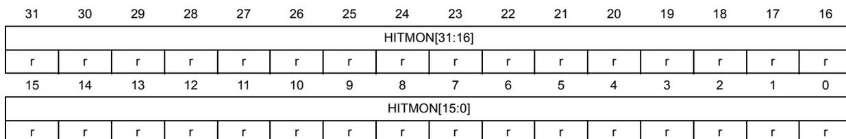
8.7.5 ICACHE hit monitor register (ICACHE_HMONR)
Address offset: 0x010
Reset value: 0x0000 0000
| 31 | 30 | 29 | 28 | 27 | 26 | 25 | 24 | 23 | 22 | 21 | 20 | 19 | 18 | 17 | 16 |
|---|---|---|---|---|---|---|---|---|---|---|---|---|---|---|---|
| HITMON[31:16] | |||||||||||||||
| r | r | r | r | r | r | r | r | r | r | r | r | r | r | r | r |
| 15 | 14 | 13 | 12 | 11 | 10 | 9 | 8 | 7 | 6 | 5 | 4 | 3 | 2 | 1 | 0 |
| HITMON[15:0] | |||||||||||||||
| r | r | r | r | r | r | r | r | r | r | r | r | r | r | r | r |
Bits 31:0 HITMON[31:0] : cache hit monitor counter
8.7.6 ICACHE miss monitor register (ICACHE_MMONR)
Address offset: 0x014
Reset value: 0x0000 0000
| 31 | 30 | 29 | 28 | 27 | 26 | 25 | 24 | 23 | 22 | 21 | 20 | 19 | 18 | 17 | 16 |
|---|---|---|---|---|---|---|---|---|---|---|---|---|---|---|---|
| Res. | Res. | Res. | Res. | Res. | Res. | Res. | Res. | Res. | Res. | Res. | Res. | Res. | Res. | Res. | Res. |
| 15 | 14 | 13 | 12 | 11 | 10 | 9 | 8 | 7 | 6 | 5 | 4 | 3 | 2 | 1 | 0 |
| MISSMON[15:0] | |||||||||||||||
| r | r | r | r | r | r | r | r | r | r | r | r | r | r | r | r |
Bits 31:16 Reserved, must be kept at reset value.
Bits 15:0 MISSMON[15:0] : cache miss monitor counter
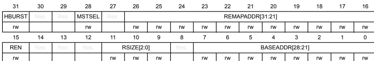
8.7.7 ICACHE region x configuration register (ICACHE_CRRx)
Address offset: 0x020 + 0x4 * x, (x = 0 to 3)
Reset value: 0x0000 0200
Define an alias address in the code region for other regions, making them cacheable.
BASEADDR and REMAPADDR fields are write locked (read only) when EN = 1 in ICACHE_CR.
| 31 | 30 | 29 | 28 | 27 | 26 | 25 | 24 | 23 | 22 | 21 | 20 | 19 | 18 | 17 | 16 |
|---|---|---|---|---|---|---|---|---|---|---|---|---|---|---|---|
| HBURST | Res. | Res. | MSTSEL | Res. | REMAPADDR[31:21] | ||||||||||
| rw | rw | rw | rw | rw | rw | rw | rw | rw | rw | rw | rw | rw | |||
| 15 | 14 | 13 | 12 | 11 | 10 | 9 | 8 | 7 | 6 | 5 | 4 | 3 | 2 | 1 | 0 |
| REN | Res. | Res. | Res. | RSIZE[2:0] | Res. | BASEADDR[28:21] | |||||||||
| rw | rw | rw | rw | rw | rw | rw | rw | rw | rw | rw | rw | ||||
Bit 31 HBURST : output burst type for region x
0: WRAP
1: INCR
Bits 30:29 Reserved, must be kept at reset value.
Bit 28 MSTSEL : AHB cache master selection for region x
0: no action (master1 selected by default)
1: master2 selected
Bit 27 Reserved, must be kept at reset value.
Bits 26:16 REMAPADDR[31:21] : remapped address for region x
This field replaces the alias address defined by BASEADDR field.
The only useful bits are [31:RI], where \( 21 \leq RI \leq 27 \) is the number of bits of RSIZE (see Section 8.4.7 ). If the programmed value has more LSBs, the useless bits are ignored.
Bit 15 REN : enable for region x
0: disabled
1: enabled
Bits 14:12 Reserved, must be kept at reset value.
Bits 11:9 RSIZE[2:0] : size for region x
000: reserved
001: 2 Mbytes
010: 4 Mbytes
011: 8 Mbytes
100: 16 Mbytes
101: 32 Mbytes
110: 64 Mbytes
111: 128 Mbytes
Bit 8 Reserved, must be kept at reset value.
Bits 7:0 BASEADDR[28:21] : base address for region x
This alias address is replaced by REMAPADDR field.
The only useful bits are [28:RI], where \( 21 \leq RI \leq 27 \) is the number of bits of RSIZE (see Section 8.4.7 ). If the programmed value has more LSBs, the useless bits are ignored.
8.7.8 ICACHE register map
Table 74. ICACHE register map and reset values
| Offset | Register name | 31 | 30 | 29 | 28 | 27 | 26 | 25 | 24 | 23 | 22 | 21 | 20 | 19 | 18 | 17 | 16 | 15 | 14 | 13 | 12 | 11 | 10 | 9 | 8 | 7 | 6 | 5 | 4 | 3 | 2 | 1 | 0 |
|---|---|---|---|---|---|---|---|---|---|---|---|---|---|---|---|---|---|---|---|---|---|---|---|---|---|---|---|---|---|---|---|---|---|
| 0x000 | ICACHE_CR | Res. | Res. | Res. | Res. | Res. | Res. | Res. | Res. | Res. | Res. | Res. | Res. | MISSMRST | HITMRST | MISSMEN | HITMEN | Res. | Res. | Res. | Res. | Res. | Res. | Res. | Res. | Res. | Res. | Res. | Res. | Res. | Res. | WAYSEL | CACHEINV |
| Reset value | 0 | 0 | 0 | 0 | 1 | 0 | |||||||||||||||||||||||||||
| 0x004 | ICACHE_SR | Res. | Res. | Res. | Res. | Res. | Res. | Res. | Res. | Res. | Res. | Res. | Res. | Res. | Res. | Res. | Res. | Res. | Res. | Res. | Res. | Res. | Res. | Res. | Res. | Res. | Res. | Res. | Res. | Res. | Res. | ERRF | BSYENDEF |
| Reset value | 0 | 1 | |||||||||||||||||||||||||||||||
| 0x008 | ICACHE_IER | Res. | Res. | Res. | Res. | Res. | Res. | Res. | Res. | Res. | Res. | Res. | Res. | Res. | Res. | Res. | Res. | Res. | Res. | Res. | Res. | Res. | Res. | Res. | Res. | Res. | Res. | Res. | Res. | Res. | Res. | ERRIE | BSYENDIE |
| Reset value | 0 | 0 | |||||||||||||||||||||||||||||||
| 0x00C | ICACHE_FCR | Res. | Res. | Res. | Res. | Res. | Res. | Res. | Res. | Res. | Res. | Res. | Res. | Res. | Res. | Res. | Res. | Res. | Res. | Res. | Res. | Res. | Res. | Res. | Res. | Res. | Res. | Res. | Res. | Res. | Res. | CERRF | BSYENDEF |
| Reset value | 0 | 0 | |||||||||||||||||||||||||||||||
| 0x010 | ICACHE_HMONR | HITMON[31:0] | |||||||||||||||||||||||||||||||
| Reset value | 0 | 0 | 0 | 0 | 0 | 0 | 0 | 0 | 0 | 0 | 0 | 0 | 0 | 0 | 0 | 0 | 0 | 0 | 0 | 0 | 0 | 0 | 0 | 0 | 0 | 0 | 0 | 0 | 0 | 0 | 0 | 0 | |
| 0x014 | ICACHE_MMONR | MISSMON[15:0] | |||||||||||||||||||||||||||||||
| Reset value | |||||||||||||||||||||||||||||||||
| 0x018-0x01C | Reserved | Reserved | |||||||||||||||||||||||||||||||
| 0x020 | ICACHE_CRR0 | HBURST | Res. | Res. | MTSEL | Res. | Res. | REMAPADDR[31:21] | REN | Res. | Res. | Res. | Res. | Res. | RSIZE [2:0] | Res. | Res. | BASEADDR[28:21] | |||||||||||||||
| Reset value | 0 | 0 | 0 | 0 | 0 | 0 | 0 | 0 | 0 | 0 | 0 | 0 | 0 | 1 | |||||||||||||||||||
| 0x024 | ICACHE_CRR1 | HBURST | Res. | Res. | MTSEL | Res. | Res. | REMAPADDR[31:21] | REN | Res. | Res. | Res. | Res. | Res. | RSIZE [2:0] | Res. | Res. | BASEADDR[28:21] | |||||||||||||||
| Reset value | 0 | 0 | 0 | 0 | 0 | 0 | 0 | 0 | 0 | 0 | 0 | 0 | 0 | 1 | |||||||||||||||||||
| 0x028 | ICACHE_CRR2 | HBURST | Res. | Res. | MTSEL | Res. | Res. | REMAPADDR[31:21] | REN | Res. | Res. | Res. | Res. | Res. | RSIZE [2:0] | Res. | Res. | BASEADDR[28:21] | |||||||||||||||
| Reset value | 0 | 0 | 0 | 0 | 0 | 0 | 0 | 0 | 0 | 0 | 0 | 0 | 0 | 1 | |||||||||||||||||||
| 0x02C | ICACHE_CRR3 | HBURST | Res. | Res. | MTSEL | Res. | Res. | REMAPADDR[31:21] | REN | Res. | Res. | Res. | Res. | Res. | RSIZE [2:0] | Res. | Res. | BASEADDR[28:21] | |||||||||||||||
| Reset value | 0 | 0 | 0 | 0 | 0 | 0 | 0 | 0 | 0 | 0 | 0 | 0 | 0 | 1 | |||||||||||||||||||