5. Global TrustZone® controller (GTZC)
Available only on STM32WBA52/54/55xx devices.
5.1 Introduction
This section describes the global TrustZone controller (GTZC) block, containing the following sub-blocks:
- •
TZSC:
TrustZone security controller
This sub-block defines the secure/privileged state of slave peripherals. The TZSC informs some peripherals (such as RCC or GPIOs) about the secure status of each securable peripheral, by sharing with RCC and I/O logic. - •
MPCBB:
memory protection controller - block based
This sub-block configures the internal RAM in a TrustZone-system product having segmented SRAM (pages of 512 bytes) with programmable-security and privileged attributes. - •
TZIC:
TrustZone illegal access controller
This sub-block gathers all illegal access events in the system and generates a secure interrupt towards NVIC.
These sub-blocks are used to configure TrustZone system security in a product having bus agents with programmable-security and privileged attributes such as:
- • on-chip RAM with programmable secure and/or privileged blocks (pages)
- • AHB and APB peripherals with programmable security and/or privileged access
- • off-chip memories with secure and/or privileged areas
5.2 GTZC main features
The GTZC main features are listed below:
- • independent 32-bit AHB interface for TZSC, TZIC, and MPCBBs
- • TZIC accessible only with secure transactions
- • Secure and nonsecure access supported for privileged and unprivileged part of TZSC and MPCBB
- • Set of registers to define product security settings:
- – Secure/privileged blocks for internal SRAMs
- – Secure/privileged access mode for securable peripherals
GTZC TrustZone system architecture
The Armv8-M supports security per TrustZone-M model with isolation between:
- • a secure world, where usually security sensitive applications are run and critical resources are located
- • a nonsecure or public world (such as usual non secure operating system and user space)
The TrustZone architecture is extended beyond AHB and Armv8-M with:
- • AHB/APB bridge used as secure gate to block or propagate secure/nonsecure and privileged/unprivileged transaction towards APB agents
- • PPC (peripheral protection controller) used as secure gate to block or propagate secure/nonsecure and privileged/unprivileged transaction towards AHB agents
- • TrustZone block-based MPC firewalls used as secure gate to filter secure/non secure, privileged/unprivileged access towards internal SRAMs
- • TrustZone watermark MPC firewalls used as secure gate to filter secure/non secure, privileged/unprivileged access towards external memories
AHB and APB Peripherals can be categorized as:
- • Privileged: peripherals protected by AHB/APB firewall stub that is controlled from TZSC to define privilege properties
- • Secure: peripherals always protected by an AHB/APB firewall stub. These peripherals are always secure (such as TZIC)
- • Securable: peripherals protected by an AHB/APB firewall stub that is controlled from TZSC to define security properties (optional)
- • Nonsecure and unprivileged: peripherals connected directly to AHB/APB interconnect without any secure gate
- • TrustZone-aware: peripherals connected directly to AHB or APB bus and implementing a specific TrustZone behavior (such as a subset of registers being secure). TrustZone-aware AHB masters always drive HNONSEC signal according to their security mode (such has Armv8-M core or DMA)
Application information
The TZSC, TZIC, and MPCBBs can be used in one of the following ways:
- • programmed during secure boot only, locked and not changed afterwards
- • dynamically re-programmed when using specific application code or secure kernel (microvisor). When not locked, MPCBB secure blocks can be changed by secure software executing from the secure FLASH region or secure SRAM. The applies to the GTZC1_TZSC_SECCFGn/PRIVCFGn registers that define secure/privileged state of each peripheral.
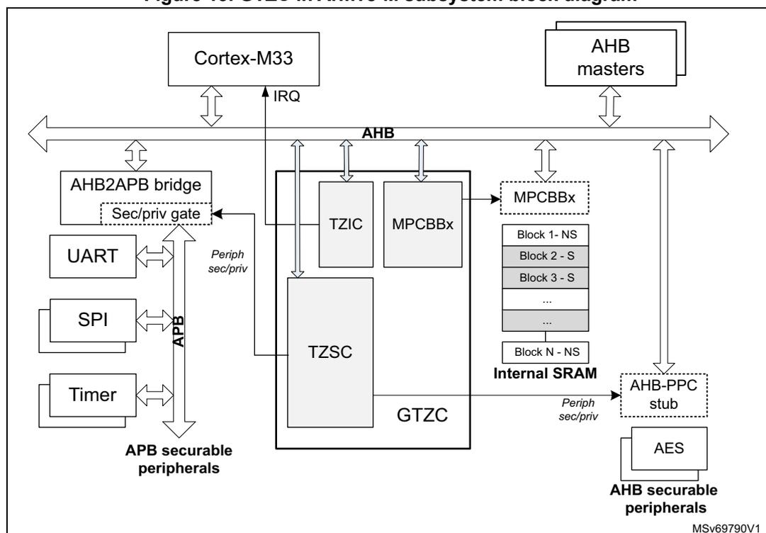
The Armv8-M security architecture with secure, securable and TrustZone-aware peripherals is shown in Figure 13 .
Figure 13. GTZC in Armv8-M subsystem block diagram
5.3 GTZC implementation
The devices embed two instances of GTZC.
Table 25. GTZC features
| GTZC sub-blocks | GTZC |
|---|---|
| TZSC | X |
| TZIC | X |
| MPCBB (number of MPCBB) | X (3) |
The following table shows the GTZC sub-blocks address offset versus GTZC base address (refer to Section 2.3 for GTZC base address).
Table 26. GTZC sub-blocks address offset
| GTZC sub-blocks | Address offset |
|---|---|
| GTZC1_TZSC | 0x0000 |
| GTZC1_TZIC | 0x0400 |
| GTZC1_MPCBB1 | 0x0800 |
| GTZC1_MPCBB2 | 0x0C00 |
| GTZC1_MPCBB6 | 0x1C00 |
The following table describes the characteristics of the available MPCBB.
Table 27. MPCBB resource assignment
| MPC | Resource | Memory size (Kbytes) | Block size (bytes) | Number of blocks | Number of super-blocks |
|---|---|---|---|---|---|
| MPCBB1 | SRAM1 | 64 (STM32WBA5xxG) | 512 | 128 | 4 |
| 32 (STM32WBA5xxE) | 64 | 2 | |||
| MPCBB2 | SRAM2 | 64 | 128 | 4 | |
| MPCBB6 | 2.4 GHz RADIO RXTXRAM | 16 | 32 | 1 |
5.4 GTZC functional description
5.4.1 GTZC block diagram
Figure 14 describes the combined feature of TZSC, TZIC, and MPCBBs. Each sub-block is controlled by its own AHB configuration port.
The TZSC defines which peripheral is secured and/or privileged. The privileged configuration bit of a peripheral can be modified by a secure privileged transaction when the peripheral is configured as secure. Otherwise, a privileged transaction (nonsecure) is sufficient.
On the opposite, the secure configuration bit of a peripheral can be modified only with a secure privileged transaction if the peripheral is configured as privileged. Otherwise, a secure transaction (unprivileged) is sufficient.
The secure configuration bit of a given ram block can be modified only with a secure privileged transaction if the same RAM block is configured as privileged. Otherwise, a secure transaction (unprivileged) is sufficient.
The TZIC gathers illegal events generated within the system when an illegal access is detected. TZIC can then generate a secure interrupt towards the CPU if needed.
Figure 14. GTZC block diagram
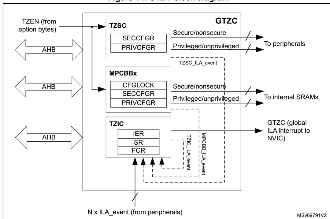
The diagram illustrates the internal structure and connections of the Global TrustZone Controller (GTZC). On the left, three AHB bus interfaces are shown. The top interface connects to the TZSC block, which also receives a 'TZEN (from option bytes)' signal. The middle interface connects to the MPCBBx block. The bottom interface connects to the TZIC block. The GTZC block itself contains these three sub-blocks. The TZSC block has 'SECCFGR' and 'PRIVCFGR' registers. The MPCBBx block has 'CFGLOCK', 'SECCFGR', and 'PRIVCFGR' registers. The TZIC block has 'IER', 'SR', and 'FCR' registers. The GTZC outputs 'Secure/nonsecure' and 'Privileged/unprivileged' signals to 'To peripherals' and 'To internal SRAMs'. It also generates 'GTZC (global ILA interrupt to NVIC)'. Dashed lines indicate 'ILA_event' signals: 'TZSC_ILA_event' from TZSC, 'MPCBB_ILA_event' from MPCBBx, and 'TZIC_ILA_event' from TZIC. All three ILA events are combined into 'N x ILA_event (from peripherals)' at the bottom. The reference 'MSv69791V2' is in the bottom right corner.
5.4.2 Illegal access definition
Three different types of illegal access (ILA) exist:
- • Illegal nonsecure access
Any nonsecure transaction trying to write a secure resource is considered as illegal: consequently, the addressed resource generates an illegal access interrupt for illegal write access and a bus error for illegal fetch access. Some exceptions exist on secure and privileged configuration registers: the latter ones authorize nonsecure read access to secure registers (see GTZC1_TZSC_SECCFGRn and GTZC1_TZSC_PRIVCFGRn).
- • Illegal secure access
Any secure transaction trying to access nonsecure block in internal block-based SRAM or watermarked memory is considered as illegal.
Correct TZIC settings enable the capture of the associated event and then generate the GTZC1_IRQn interrupt to the NVIC. This applies to read, write, and execute accesses.
Concerning the MPCBB controller, there is an option to ignore secure data read/write access on nonsecure SRAM blocks, by setting the SRWILADIS bit in the GTZC1_MPCBB_CR register. Secure read and write data transactions are then allowed on nonsecure SRAM blocks, while secure execution access remains not allowed.
Any secure execute transaction trying to access a nonsecure peripheral register is considered as illegal and generates a bus error.
- • Illegal unprivileged access
Any unprivileged transaction trying to access a privileged resource is considered as illegal. There is no illegal access event generated for illegal read and write access. The
addressed resource follows a silent-fail behavior, returning all zero data for read and ignoring any write. No bus error is generated. A bus error is generated when any unprivileged execute transaction tries to access a privileged memory.
5.4.3 TrustZone security controller (TZSC)
The TZSC is composed of a configurable set of registers, providing the control of secure and privileged state for all peripherals, done through:
- • GTZC1_TZSC_SECCFGn registers to control AHB/APB firewall stubs for the securable peripherals
- • GTZC1_TZSC_PRIVCFGn registers to control AHB/APB firewall stubs for the privileged peripherals
5.4.4 Memory protection controller - block based (MPCBB)
The MPCBB is composed of a configurable set of registers allowing security and privileged policy to be defined for internal SRAM memories. The security and privileged policy can be individually configured per each 512-byte block of SRAM.
Figure 15. MPCBB block diagram
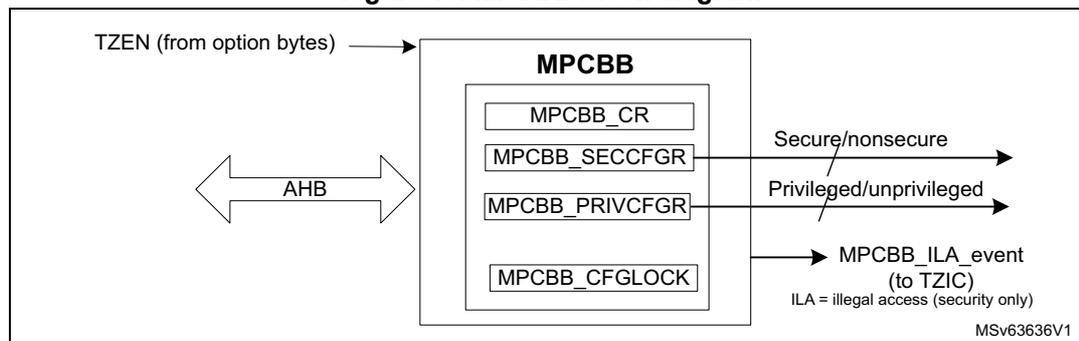
In order to set up the MPCBB, the following actions are needed (for example at boot time):
- • Secure firmware must define which memory blocks are secure by setting the correct bits in GTZC1_MPCBB_SECCFGn.
- • Privileged firmware must define which memory blocks are privileged by setting the correct bits in GTZC1_MPCBB_PRIVCFGn.
An MPCBB super-block is made of 32 consecutive blocks. For each super-block, a secure application can lock all related secure/privileged bits using the correct bits in GTZC1_MPCBB_CFGLOCK. This lock remains active until the next system reset.
Note: The block size is 512 bytes. The super-block size is 512 x 32 = 16 Kbytes.
5.4.5 TrustZone illegal access controller (TZIC)
The TZIC concentrates all illegal access source events. It is used only when the system is TrustZone enabled (TZEN = 1).
TZIC allows the trace (flag) of which event triggered the secure illegal access interrupt. Register masks (GTZC1_TZIC_IERx) are available to filter unwanted event. On unmasked illegal event, TZIC generates the GTZC1_IRQn interrupt to the NVIC.
For each illegal event source, a status flag and a clear bit exist (respectively within GTZC1_TZIC_SRx and GTZC1_TZIC_FCRx). The reset value of mask registers (GTZC1_TZIC_IERx) is such that all events are masked.
5.4.6 Power-on/reset state
The power-on and reset state of the TZSC clear to 0 all bits of GTZC1_TZSC_SECCFGRn and GTZC1_TZSC_PRIVCFGRn, meaning that all securable peripherals are respectively set to nonsecure and unprivileged.
For internal SRAMs, all GTZC1_MPCBB_SECCFGRn and GTZC1_MPCBB_PRIVCFGRn are set:
- • to 0xFFFF FFFF, making these internal memories block secure and privileged by default when TrustZone security is enabled at system level (TZEN = 1)
- • to 0x0000 0000, making these internal memories block nonsecure and unprivileged by default when TrustZone security is disabled at system level (TZEN = 0)
Secure boot code can then program the security settings, making components secure or not as needed.
5.5 GTZC interrupts
TZIC is a secure peripheral, which systematically generates an illegal access event when accessed by a nonsecure access. The MPCBB and TZSC are TrustZone-aware peripherals, meaning that secure and nonsecure registers coexist within the peripheral.
Table 28. GTZC interrupt request
| Interrupt acronym | Interrupt event | Event flag | Enable control bit | Interrupt clear method | Exit Sleep mode | Exit Stop mode | Exit Standby mode |
|---|---|---|---|---|---|---|---|
| GTZC | Illegal access | All flags in GTZC1_TZIC_SRx | All bits in GTZC1_TZIC_IERx | Write 1 in the bit GTZC1_TZIC_FCRx | Yes | No | No |
5.6 GTZC1 TZSC registers
All registers are accessed only by words (32-bit).
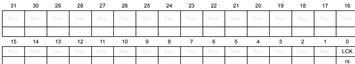
5.6.1 GTZC1 TZSC control register (GTZC1_TZSC_CR)
Address offset: 0x000
Reset value: 0x0000 0000
Secure privileged access only.
| 31 | 30 | 29 | 28 | 27 | 26 | 25 | 24 | 23 | 22 | 21 | 20 | 19 | 18 | 17 | 16 |
| Res. | Res. | Res. | Res. | Res. | Res. | Res. | Res. | Res. | Res. | Res. | Res. | Res. | Res. | Res. | Res. |
| 15 | 14 | 13 | 12 | 11 | 10 | 9 | 8 | 7 | 6 | 5 | 4 | 3 | 2 | 1 | 0 |
| Res. | Res. | Res. | Res. | Res. | Res. | Res. | Res. | Res. | Res. | Res. | Res. | Res. | Res. | Res. | LCK |
| rs |
Bits 31:1 Reserved, must be kept at reset value.
Bit 0 LCK : Lock the configuration of GTZC1_TZSC_SECCFGRn and GTZC1_TZSC_PRIVCFGRn registers until next reset
This bit is cleared by default and once set, it can not be reset until system reset.
0: Configuration of all GTZC1_TZSC_SECCFGRn and GTZC1_TZSC_PRIVCFGRn registers not locked
1: Configuration of all GTZC1_TZSC_SECCFGRn and GTZC1_TZSC_PRIVCFGRn registers locked
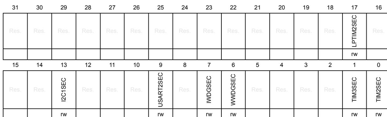
5.6.2 GTZC1 TZSC secure configuration register 1 (GTZC1_TZSC_SECCFGR1)
Address offset: 0x010
Reset value: 0x0000 0000
Write-secure access only.
This register can be written only by secure privileged transaction when the corresponding GTZC1_TZSC_PRIVCFGR1 register bit is set to 1. If a given PRIV bit is not set, the equivalent SEC bit can be written by secure unprivileged transaction.
Read accesses are authorized for any type of transactions, secure or not, privileged or not.
| 31 | 30 | 29 | 28 | 27 | 26 | 25 | 24 | 23 | 22 | 21 | 20 | 19 | 18 | 17 | 16 |
| Res. | Res. | Res. | Res. | Res. | Res. | Res. | Res. | Res. | Res. | Res. | Res. | Res. | Res. | LPTIM2SEC | Res. |
| rw | |||||||||||||||
| 15 | 14 | 13 | 12 | 11 | 10 | 9 | 8 | 7 | 6 | 5 | 4 | 3 | 2 | 1 | 0 |
| Res. | Res. | I2C1SEC | Res. | Res. | Res. | USART2SEC | Res. | IWDGSEC | WWDGSEC | Res. | Res. | Res. | Res. | TIM3SEC | TIM2SEC |
| rw | rw | rw | rw | rw | rw |
Bits 31:18 Reserved, must be kept at reset value.
Bit 17 LPTIM2SEC : Secure access mode for LPTIM2
0: Nonsecure
1: Secure
Bits 16:14 Reserved, must be kept at reset value.
Bit 13 I2C1SEC : Secure access mode for I2C1
0: Nonsecure
1: Secure
Bits 12:10 Reserved, must be kept at reset value.
Bit 9 USART2SEC : Secure access mode for USART2
0: Nonsecure
1: Secure
Bit 8 Reserved, must be kept at reset value.
Bit 7 IWDGSEC : Secure access mode for IWDG
0: Nonsecure
1: Secure
Bit 6 WWDGSEC : Secure access mode for WWDG
0: Nonsecure
1: Secure
Bits 5:2 Reserved, must be kept at reset value.
Bit 1 TIM3SEC : Secure access mode for TIM3
0: Nonsecure
1: Secure
Bit 0 TIM2SEC : Secure access mode for TIM2
0: Nonsecure
1: Secure
5.6.3 GTZC1 TZSC secure configuration register 2 (GTZC1_TZSC_SECCFGR2)
Address offset: 0x014
Reset value: 0x0000 0000
Write-secure access only.
This register can be written only by secure privileged transaction when the corresponding GTZC1_TZSC_PRIVCFG2 register bit is set to 1. If a given PRIV is not set, the equivalent SEC bit can be written by secure unprivileged transaction.
Read accesses are authorized for any type of transactions, secure or not, privileged or not.
| 31 | 30 | 29 | 28 | 27 | 26 | 25 | 24 | 23 | 22 | 21 | 20 | 19 | 18 | 17 | 16 |
|---|---|---|---|---|---|---|---|---|---|---|---|---|---|---|---|
| Res. | Res. | Res. | Res. | Res. | Res. | Res. | ADC4SEC | COMPSEC | Res. | Res. | Res. | LPTIM1SEC | I2C3SEC | LPUART1SEC | SPI3SEC |
| nw | nw | nw | nw | nw | nw | ||||||||||
| 15 | 14 | 13 | 12 | 11 | 10 | 9 | 8 | 7 | 6 | 5 | 4 | 3 | 2 | 1 | 0 |
| Res. | Res. | Res. | Res. | Res. | Res. | Res. | Res. | SA11SEC | TIM17SEC | TIM16SEC | Res. | USART1SEC | Res. | SPI1SEC | TIM1SEC |
| nw | nw | nw | nw | nw | nw |
Bits 31:25 Reserved, must be kept at reset value.
Bit 24 ADC4SEC : Secure access mode for ADC4
0: Nonsecure
1: Secure
Bit 23 COMPSEC : Secure access mode for COMP
0: Nonsecure
1: Secure
Note that bit 23 is reserved on STM32WBA52xx devices.
Bits 22:20 Reserved, must be kept at reset value.
Bit 19 LPTIM1SEC : Secure access mode for LPTIM1
0: Nonsecure
1: Secure
Bit 18 I2C3SEC : Secure access mode for I2C3
0: Nonsecure
1: Secure
Bit 17 LPUART1SEC : Secure access mode for LPUART1
0: Nonsecure
1: Secure
Bit 16 SPI3SEC : Secure access mode for SPI3
0: Nonsecure
1: Secure
Bits 15:8 Reserved, must be kept at reset value.
Bit 7 SA11SEC : Secure access mode for SA11
0: Nonsecure
1: Secure
Note that bit 7 is reserved on STM32WBA52xx devices.
Bit 6 TIM17SEC : Secure access mode for TIM17
0: Nonsecure
1: Secure
Bit 5 TIM16SEC : Secure access mode for TIM16
0: Nonsecure
1: Secure
Bit 4 Reserved, must be kept at reset value.
Bit 3 USART1SEC : Secure access mode for USART1
0: Nonsecure
1: Secure
Bit 2 Reserved, must be kept at reset value.
Bit 1 SPI1SEC : Secure access mode for SPI1
0: Nonsecure
1: Secure
Bit 0 TIM1SEC : Secure access mode for TIM1
0: Nonsecure
1: Secure
5.6.4 GTZC1 TZSC secure configuration register 3 (GTZC1_TZSC_SECCFGR3)
Address offset: 0x018
Reset value: 0x0000 0000
Write-secure access only.
This register can be written only by secure privileged transaction when the corresponding GTZC1_TZSC_PRIVCFGR3 register bit is set to 1. If a given PRIV is not set, the equivalent SEC bit can be written by secure unprivileged transaction.
Read accesses are authorized for any type of transactions, secure or not, privileged or not.
| 31 | 30 | 29 | 28 | 27 | 26 | 25 | 24 | 23 | 22 | 21 | 20 | 19 | 18 | 17 | 16 |
|---|---|---|---|---|---|---|---|---|---|---|---|---|---|---|---|
| Res. | Res. | Res. | Res. | Res. | Res. | Res. | PTCONVSEC | RADIOSEC | RAMCFGSEC | Res. | Res. | Res. | Res. | Res. | PKASEC |
| rw | rw | rw | rw | ||||||||||||
| 15 | 14 | 13 | 12 | 11 | 10 | 9 | 8 | 7 | 6 | 5 | 4 | 3 | 2 | 1 | 0 |
| Res. | SAESSEC | RNGSEC | HASHSEC | AESSEC | Res. | Res. | Res. | Res. | ICACHE_REGSEC | Res. | TSCSEC | CRCSEC | Res. | Res. | Res. |
| rw | rw | rw | rw | rw | rw | rw |
Bits 31:25 Reserved, must be kept at reset value.
- Bit 24
PTACONVSEC
: Secure access mode for PTACONV
0: Nonsecure
1: Secure
Note that bit 24 is reserved on STM32WBA52xx devices. - Bit 23
RADIOSEC
: Secure access mode for 2.4 GHz RADIO
0: Nonsecure
1: Secure - Bit 22
RAMCFGSEC
: Secure access mode for RAMCFG
0: Nonsecure
1: Secure - Bits 21:17 Reserved, must be kept at reset value.
- Bit 16
PKASEC
: Secure access mode for PKA
0: Nonsecure
1: Secure - Bit 15 Reserved, must be kept at reset value.
- Bit 14
SAESSEC
: Secure access mode for SAES
0: Nonsecure
1: Secure - Bit 13
RNGSEC
: Secure access mode for RNG
0: Nonsecure
1: Secure - Bit 12
HASHSEC
: Secure access mode for HASH
0: Nonsecure
1: Secure - Bit 11
AESSEC
: Secure access mode for AES
0: Nonsecure
1: Secure - Bits 10:7 Reserved, must be kept at reset value.
- Bit 6
ICACHE_REGSEC
: Secure access mode for ICACHE registers
0: Nonsecure
1: Secure - Bit 5 Reserved, must be kept at reset value.
- Bit 4
TSCSEC
: Secure access mode for TSC
0: Nonsecure
1: Secure - Bit 3
CRCSEC
: Secure access mode for CRC
0: Nonsecure
1: Secure - Bits 2:0 Reserved, must be kept at reset value.
5.6.5 GTZC1 TZSC privilege configuration register 1 (GTZC1_TZSC_PRIVCFGR1)
Address offset: 0x020
Reset value: 0x0000 0000
Write-privileged access only.
This register can be written only by secure privileged transaction when the corresponding GTZC1_TZSC_SECCFGR1 register bit is set to 1. If a given SEC bit is not set, the equivalent PRIV bit can be written by nonsecure privileged transaction.
Read accesses are authorized for any type of transactions, secure or not, privileged or not.
| 31 | 30 | 29 | 28 | 27 | 26 | 25 | 24 | 23 | 22 | 21 | 20 | 19 | 18 | 17 | 16 |
|---|---|---|---|---|---|---|---|---|---|---|---|---|---|---|---|
| Res. | Res. | Res. | Res. | Res. | Res. | Res. | Res. | Res. | Res. | Res. | Res. | Res. | Res. | LPTIM2PRIV | Res. |
| r/w | |||||||||||||||
| 15 | 14 | 13 | 12 | 11 | 10 | 9 | 8 | 7 | 6 | 5 | 4 | 3 | 2 | 1 | 0 |
| Res. | Res. | I2C1PRIV | Res. | Res. | Res. | USART2PRIV | Res. | IWDGPRIV | WWDGPRIV | Res. | Res. | Res. | Res. | TIM3PRIV | TIM2PRIV |
| r/w | r/w | r/w | r/w | r/w | r/w |
Bits 31:18 Reserved, must be kept at reset value.
Bit 17 LPTIM2PRIV : Privileged access mode for LPTIM2
0: Unprivileged
1: Privileged
Bits 16:14 Reserved, must be kept at reset value.
Bit 13 I2C1PRIV : Privileged access mode for I2C1
0: Unprivileged
1: Privileged
Bits 12:10 Reserved, must be kept at reset value.
Bit 9 USART2PRIV : Privileged access mode for USART2
0: Unprivileged
1: Privileged
Bit 8 Reserved, must be kept at reset value.
Bit 7 IWDGPRIV : Privileged access mode for IWDG
0: Unprivileged
1: Privileged
Bit 6 WWDGPRIV : Privileged access mode for WWDG
0: Unprivileged
1: Privileged
Bits 5:2 Reserved, must be kept at reset value.
Bit 1 TIM3PRIV : Privileged access mode for TIM3
0: Unprivileged
1: Privileged
Bit 0 TIM2PRIV : Privileged access mode for TIM2
0: Unprivileged
1: Privileged
5.6.6 GTZC1 TZSC privilege configuration register 2 (GTZC1_TZSC_PRIVCFGR2)
Address offset: 0x024
Reset value: 0x0000 0000
Write-privileged access only.
This register can be written only by secure privileged transaction when the corresponding GTZC1_TZSC_SECCFGR2 register bit is set to 1. If a given SEC bit is not set, the equivalent PRIV bit can be written by nonsecure privileged transaction.
Read accesses are authorized for any type of transactions, secure or not, privileged or not.
| 31 | 30 | 29 | 28 | 27 | 26 | 25 | 24 | 23 | 22 | 21 | 20 | 19 | 18 | 17 | 16 |
|---|---|---|---|---|---|---|---|---|---|---|---|---|---|---|---|
| Res. | Res. | Res. | Res. | Res. | Res. | Res. | ADC4PRIV | COMPPRIV | Res. | Res. | Res. | LPTIM1PRIV | I2C3PRIV | LPUART1PRIV | SPI3PRIV |
| rw | rw | rw | rw | rw | rw |
| 15 | 14 | 13 | 12 | 11 | 10 | 9 | 8 | 7 | 6 | 5 | 4 | 3 | 2 | 1 | 0 |
|---|---|---|---|---|---|---|---|---|---|---|---|---|---|---|---|
| Res. | Res. | Res. | Res. | Res. | Res. | Res. | Res. | SAH1PRIV | TIM7PRIV | TIM16PRIV | Res. | USART1PRIV | Res. | SPI1PRIV | TIM1PRIV |
| rw | rw | rw | rw | rw | rw |
Bits 31:25 Reserved, must be kept at reset value.
Bit 24 ADC4PRIV : Privileged access mode for ADC4
0: Unprivileged
1: Privileged
Bit 23 COMPPRIV : Privileged access mode for COMP
0: Unprivileged
1: Privileged
Note that bit 23 is reserved on STM32WBA52xx devices.
Bits 22:20 Reserved, must be kept at reset value.
Bit 19 LPTIM1PRIV : Privileged access mode for LPTIM1
0: Unprivileged
1: Privileged
Bit 18 I2C3PRIV : Privileged access mode for I2C3
0: Unprivileged
1: Privileged
Bit 17 LPUART1PRIV : Privileged access mode for LPUART1
0: Unprivileged
1: Privileged
Bit 16 SPI3PRIV : Privileged access mode for SPI3
0: Unprivileged
1: Privileged
Bits 15:8 Reserved, must be kept at reset value.
Bit 7 SAI1PRIV : Privileged access mode for SAI1
0: Unprivileged
1: Privileged
Note that bit 7 is reserved on STM32WBA52xx devices.
Bit 6 TIM17PRIV : Privileged access mode for TIM17
0: Unprivileged
1: Privileged
Bit 5 TIM16PRIV : Privileged access mode for TIM16
0: Unprivileged
1: Privileged
Bit 4 Reserved, must be kept at reset value.
Bit 3 USART1PRIV : Privileged access mode for USART1
0: Unprivileged
1: Privileged
Bit 2 Reserved, must be kept at reset value.
Bit 1 SPI1PRIV : Privileged access mode for SPI1PRIV
0: Unprivileged
1: Privileged
Bit 0 TIM1PRIV : Privileged access mode for TIM1
0: Unprivileged
1: Privileged
5.6.7 GTZC1 TZSC privilege configuration register 3 (GTZC1_TZSC_PRIVCFGR3)
Address offset: 0x028
Reset value: 0x0000 0000
Write-privileged access only.
This register can be written only by secure privileged transaction when the corresponding GTZC1_TZSC_SECCFGR3 register bit is set to 1. If a given SEC bit is not set, the equivalent PRIV bit can be written by nonsecure privileged transaction.
Read accesses are authorized for any type of transactions, secure or not, privileged or not.
| 31 | 30 | 29 | 28 | 27 | 26 | 25 | 24 | 23 | 22 | 21 | 20 | 19 | 18 | 17 | 16 |
|---|---|---|---|---|---|---|---|---|---|---|---|---|---|---|---|
| Res. | Res. | Res. | Res. | Res. | Res. | Res. | PTACONVPRIV | RADIOPRIV | RAMCFGPRIV | Res. | Res. | Res. | Res. | Res. | PKAPRIV |
| rw | rw | rw | rw | ||||||||||||
| 15 | 14 | 13 | 12 | 11 | 10 | 9 | 8 | 7 | 6 | 5 | 4 | 3 | 2 | 1 | 0 |
| Res. | SAESPRIV | RNGPRIV | HASHPRIV | AESPRIV | Res. | Res. | Res. | Res. | ICACHE_REGPRIV | Res. | TSCPRIV | CRCPRIV | Res. | Res. | Res. |
| rw | rw | rw | rw | rw | rw | rw |
Bits 31:25 Reserved, must be kept at reset value.
Bit 24 PTACONVPRIV : Privileged access mode for PTACONV
0: Unprivileged
1: Privileged
Note that bit 24 is reserved on STM32WBA52xx devices.
Bit 23 RADIOPRIV : Privileged access mode for 2.4 GHz RADIO
0: Unprivileged
1: Privileged
Bit 22 RAMCFGPRIV : Privileged access mode for RAMCFG
0: Unprivileged
1: Privileged
Bits 21:17 Reserved, must be kept at reset value.
Bit 16 PKAPRIV : Privileged access mode for PKA
0: Unprivileged
1: Privileged
Bit 15 Reserved, must be kept at reset value.
Bit 14 SAESPRIV : Privileged access mode for SAES
0: Unprivileged
1: Privileged
Bit 13 RNGPRIV : Privileged access mode for RNG
0: Unprivileged
1: Privileged
Bit 12 HASHPRIV : Privileged access mode for HASH
0: Unprivileged
1: Privileged
Bit 11 AESPRIV : Privileged access mode for AES
0: Unprivileged
1: Privileged
Bits 10:7 Reserved, must be kept at reset value.
Bit 6 ICACHE_REGPRIV : Privileged access mode for ICACHE registers
0: Unprivileged
1: Privileged
Bit 5 Reserved, must be kept at reset value.
Bit 4 TSCPRIV : Privileged access mode for TSC
0: Unprivileged
1: Privileged
Bit 3 CRCPRIV : Privileged access mode for CRC
0: Unprivileged
1: Privileged
Bits 2:0 Reserved, must be kept at reset value.
5.6.8 GTZC1 TZSC register map
Table 29. GTZC1 TZSC register map and reset values
| Offset | Register | 31 | 30 | 29 | 28 | 27 | 26 | 25 | 24 | 23 | 22 | 21 | 20 | 19 | 18 | 17 | 16 | 15 | 14 | 13 | 12 | 11 | 10 | 9 | 8 | 7 | 6 | 5 | 4 | 3 | 2 | 1 | 0 |
|---|---|---|---|---|---|---|---|---|---|---|---|---|---|---|---|---|---|---|---|---|---|---|---|---|---|---|---|---|---|---|---|---|---|
| 0x000 | GTZC1_TZSC_CR | Res | Res | Res | Res | Res | Res | Res | Res | Res | Res | Res | Res | Res | Res | Res | Res | Res | Res | Res | Res | Res | Res | Res | Res | Res | Res | Res | Res | Res | Res | Res | 0 |
| Reset value | LCK | ||||||||||||||||||||||||||||||||
| 0x004 to 0x00C | Reserved | Reserved | |||||||||||||||||||||||||||||||
| 0x010 | GTZC1_TZSC_SECCFGGR1 | Res | Res | Res | Res | Res | Res | Res | Res | Res | Res | Res | Res | Res | Res | LPTIM2SEC | Res | Res | Res | Res | I2C1SEC | Res | Res | USART2SEC | Res | Res | Res | Res | Res | Res | Res | Res | |
| Reset value | 0 | 0 | 0 | 0 | 0 | ||||||||||||||||||||||||||||
| 0x014 | GTZC1_TZSC_SECCFGGR2 | Res | Res | Res | Res | Res | Res | Res | Res | Res | Res | Res | Res | Res | Res | Res | Res | Res | Res | Res | Res | Res | Res | Res | Res | Res | Res | Res | Res | Res | Res | Res | Res |
| Reset value | 0 | 0 | |||||||||||||||||||||||||||||||
| 0x018 | GTZC1_TZSC_SECCFGGR3 | Res | Res | Res | Res | Res | Res | Res | Res | Res | Res | Res | Res | Res | Res | Res | Res | Res | Res | Res | Res | Res | Res | Res | Res | Res | Res | Res | Res | Res | Res | Res | Res |
| Reset value | 0 | 0 | |||||||||||||||||||||||||||||||
| 0x01C | Reserved | Reserved | |||||||||||||||||||||||||||||||
| 0x020 | GTZC1_TZSC_PRIVCFGGR1 | Res | Res | Res | Res | Res | Res | Res | Res | Res | Res | Res | Res | Res | Res | LPTIM2PRIV | Res | Res | Res | Res | I2C1PRIV | Res | Res | USART2PRIV | Res | Res | Res | Res | Res | Res | Res | Res | |
| Reset value | 0 | 0 | 0 | 0 | 0 | ||||||||||||||||||||||||||||
| 0x024 | GTZC1_TZSC_PRIVCFGGR2 | Res | Res | Res | Res | Res | Res | Res | Res | Res | Res | Res | Res | Res | Res | Res | Res | Res | Res | Res | Res | Res | Res | Res | Res | Res | Res | Res | Res | Res | Res | Res | Res |
| Reset value | 0 | 0 | |||||||||||||||||||||||||||||||
| 0x028 | GTZC1_TZSC_PRIVCFGGR3 | Res | Res | Res | Res | Res | Res | Res | Res | Res | Res | Res | Res | Res | Res | Res | Res | Res | Res | Res | Res | Res | Res | Res | Res | Res | Res | Res | Res | Res | Res | Res | Res |
| Reset value | 0 | 0 | |||||||||||||||||||||||||||||||
1. Bit(s) reserved on STM32WBA52xx devices.
Refer to Table 26: GTZC sub-blocks address offset .5.7 GTZC1 TZIC registers
All registers are accessed only by words (32-bit).
5.7.1 GTZC1 TZIC interrupt enable register 1 (GTZC1_TZIC_IER1)
Address offset: 0x000
Reset value: 0x0000 0000
Secure privileged access only.
This register is used to enable interrupt of illegal access.
| 31 | 30 | 29 | 28 | 27 | 26 | 25 | 24 | 23 | 22 | 21 | 20 | 19 | 18 | 17 | 16 |
|---|---|---|---|---|---|---|---|---|---|---|---|---|---|---|---|
| Res. | Res. | Res. | Res. | Res. | Res. | Res. | Res. | Res. | Res. | Res. | Res. | Res. | Res. | LPTIM2IE | Res. |
| rw | |||||||||||||||
| 15 | 14 | 13 | 12 | 11 | 10 | 9 | 8 | 7 | 6 | 5 | 4 | 3 | 2 | 1 | 0 |
| Res. | Res. | I2C1IE | Res. | Res. | Res. | USART2IE | Res. | IWDGIE | WWDGIE | Res. | Res. | Res. | Res. | TIM3IE | TIM2IE |
| rw | rw | rw | rw | rw | rw |
Bits 31:18 Reserved, must be kept at reset value.
Bit 17 LPTIM2IE : Illegal access interrupt enable for LPTIM2
0: Interrupt disabled
1: Interrupt enabled
Bits 16:14 Reserved, must be kept at reset value.
Bit 13 I2C1IE : Illegal access interrupt enable for I2C1
0: Interrupt disabled
1: Interrupt enabled
Bits 12:10 Reserved, must be kept at reset value.
Bit 9 USART2IE : Illegal access interrupt enable for USART2
0: Interrupt disabled
1: Interrupt enabled
Bit 8 Reserved, must be kept at reset value.
Bit 7 IWDGIE : Illegal access interrupt enable for IWDG
0: Interrupt disabled
1: Interrupt enabled
Bit 6 WWDGIE : Illegal access interrupt enable for WWDG
0: Interrupt disabled
1: Interrupt enabled
Bits 5:2 Reserved, must be kept at reset value.
Bit 1 TIM3IE : Illegal access interrupt enable for TIM3
0: Interrupt disabled
1: Interrupt enabled
Bit 0 TIM2IE : Illegal access interrupt enable for TIM2
0: Interrupt disabled
1: Interrupt enabled
5.7.2 GTZC1 TZIC interrupt enable register 2 (GTZC1_TZIC_IER2)
Address offset: 0x004
Reset value: 0x0000 0000
Secure privileged access only.
This register is used to enable interrupt of illegal access.
| 31 | 30 | 29 | 28 | 27 | 26 | 25 | 24 | 23 | 22 | 21 | 20 | 19 | 18 | 17 | 16 |
|---|---|---|---|---|---|---|---|---|---|---|---|---|---|---|---|
| Res. | Res. | Res. | Res. | Res. | Res. | Res. | ADC4IE | COMPIE | Res. | Res. | Res. | LPTIM1IE | I2C3IE | LPUART1IE | SPI3IE |
| 15 | 14 | 13 | 12 | 11 | 10 | 9 | 8 | 7 | 6 | 5 | 4 | 3 | 2 | 1 | 0 |
| Res. | Res. | Res. | Res. | Res. | Res. | Res. | Res. | SA11IE | TIM17IE | TIM16IE | Res. | USART1IE | Res. | SP11IE | TIM1IE |
| rw | rw | rw | rw | rw | rw |
Bits 31:25 Reserved, must be kept at reset value.
Bit 24 ADC4IE : Illegal access interrupt enable for ADC4
0: Interrupt disabled
1: Interrupt enabled
Bit 23 COMPIE : Illegal access interrupt enable for COMP
0: Interrupt disabled
1: Interrupt enabled
Note that bit 23 is reserved on STM32WBA52xx devices.
Bits 22:20 Reserved, must be kept at reset value.
Bit 19 LPTIM1IE : Illegal access interrupt enable for LPTIM1
0: Interrupt disabled
1: Interrupt enabled
Bit 18 I2C3IE : Illegal access interrupt enable for I2C3
0: Interrupt disabled
1: Interrupt enabled
Bit 17 LPUART1IE : Illegal access interrupt enable for LPUART1
0: Interrupt disabled
1: Interrupt enabled
Bit 16 SPI3IE : Illegal access interrupt enable for SPI3
0: Interrupt disabled
1: Interrupt enabled
Bits 15:8 Reserved, must be kept at reset value.
- Bit 7
SAI1IE
: Illegal access interrupt enable for SAI1
0: Interrupt disabled
1: Interrupt enabled
Note that bit 7 is reserved on STM32WBA52xx devices. - Bit 6
TIM17IE
: Illegal access interrupt enable for TIM17
0: Interrupt disabled
1: Interrupt enabled - Bit 5
TIM16IE
: Illegal access interrupt enable for TIM16
0: Interrupt disabled
1: Interrupt enabled - Bit 4 Reserved, must be kept at reset value.
- Bit 3
USART1IE
: Illegal access interrupt enable for USART1
0: Interrupt disabled
1: Interrupt enabled - Bit 2 Reserved, must be kept at reset value.
- Bit 1
SPI1IE
: Illegal access interrupt enable for SPI1
0: Interrupt disabled
1: Interrupt enabled - Bit 0
TIM1IE
: Illegal access interrupt enable for TIM1
0: Interrupt disabled
1: Interrupt enabled
5.7.3 GTZC1 TZIC interrupt enable register 3 (GTZC1_TZIC_IER3)
Address offset: 0x008
Reset value: 0x0000 0000
Secure privileged access only.
This register is used to enable interrupt of illegal access.
| 31 | 30 | 29 | 28 | 27 | 26 | 25 | 24 | 23 | 22 | 21 | 20 | 19 | 18 | 17 | 16 |
|---|---|---|---|---|---|---|---|---|---|---|---|---|---|---|---|
| Res. | Res. | Res. | Res. | Res. | Res. | Res. | PTACONVIE | RADIOIE | RAMCFGIE | Res. | Res. | Res. | Res. | Res. | PKAIE |
| r/w | r/w | r/w | r/w | ||||||||||||
| 15 | 14 | 13 | 12 | 11 | 10 | 9 | 8 | 7 | 6 | 5 | 4 | 3 | 2 | 1 | 0 |
| HSEMIIE | SAESIE | RNGIE | HASHIE | AESIE | Res. | Res. | Res. | Res. | ICACHEIE | Res. | TSCIE | CRCIE | Res. | Res. | Res. |
| r/w | r/w | r/w | r/w | r/w | r/w | r/w | r/w |
Bits 31:25 Reserved, must be kept at reset value.
- Bit 24
PTACONVIE
: Illegal access interrupt enable for PTACONV
0: Interrupt disabled
1: Interrupt enabled
Note that bit 24 is reserved on STM32WBA52xx devices.
- Bit 23
RADIOIE
: Illegal access interrupt enable for 2.4 GHz RADIO
0: Interrupt disabled
1: Interrupt enabled - Bit 22
RAMCFGIE
: Illegal access interrupt enable for RAMCFG
0: Interrupt disabled
1: Interrupt enabled - Bits 21:17 Reserved, must be kept at reset value.
- Bit 16
PKAIE
: Illegal access interrupt enable for PKA
0: Interrupt disabled
1: Interrupt enabled - Bit 15
HSEME
: Illegal access interrupt enable for HSEM
0: Interrupt disabled
1: Interrupt enabled - Bit 14
SAESIE
: Illegal access interrupt enable for SAES
0: Interrupt disabled
1: Interrupt enabled - Bit 13
RNGIE
: Illegal access interrupt enable for RNG
0: Interrupt disabled
1: Interrupt enabled - Bit 12
HASHIE
: Illegal access interrupt enable for HASH
0: Interrupt disabled
1: Interrupt enabled - Bit 11
AESIE
: Illegal access interrupt enable for AES
0: Interrupt disabled
1: Interrupt enabled - Bits 10:7 Reserved, must be kept at reset value.
- Bit 6
ICACHEIE
: Illegal access interrupt enable for ICACHE registers
0: Interrupt disabled
1: Interrupt enabled - Bit 5 Reserved, must be kept at reset value.
- Bit 4
TSCIE
: Illegal access interrupt enable for TSC
0: Interrupt disabled
1: Interrupt enabled - Bit 3
CRCIE
: Illegal access interrupt enable for CRC
0: Interrupt disabled
1: Interrupt enabled - Bits 2:0 Reserved, must be kept at reset value.
5.7.4 GTZC1 TZIC interrupt enable register 4 (GTZC1_TZIC_IER4)
Address offset: 0x00C
Reset value: 0x0000 0000
Secure privileged access only.
This register is used to enable interrupt of illegal access.
| 31 | 30 | 29 | 28 | 27 | 26 | 25 | 24 | 23 | 22 | 21 | 20 | 19 | 18 | 17 | 16 |
|---|---|---|---|---|---|---|---|---|---|---|---|---|---|---|---|
| MPCBB6IE | SRAM6IE | Res. | Res. | Res. | Res. | MPCBB2IE | SRAM2IE | MPCBB1IE | SRAM1IE | Res. | Res. | Res. | Res. | Res. | Res. |
| rw | rw | rw | rw | rw | rw | ||||||||||
| 15 | 14 | 13 | 12 | 11 | 10 | 9 | 8 | 7 | 6 | 5 | 4 | 3 | 2 | 1 | 0 |
| TZICIE | TZSCIE | EXTIIE | Res. | RCCIE | PWRIE | TAMPIE | RTCIE | SYSCFGIE | Res. | Res. | Res. | Res. | FLASH_REGIE | FLASHIE | GPDMA1IE |
| rw | rw | rw | rw | rw | rw | rw | rw | rw | rw | rw |
Bit 31 MPCBB6IE : Illegal access interrupt enable for MPCBB6
0: Interrupt disabled
1: Interrupt enabled
Bit 30 SRAM6IE : Illegal access interrupt enable for 2.4 GHz RXTXRAM memory
0: Interrupt disabled
1: Interrupt enabled
Bits 29:26 Reserved, must be kept at reset value.
Bit 25 MPCBB2IE : Illegal access interrupt enable for MPCBB2
0: Interrupt disabled
1: Interrupt enabled
Bit 24 SRAM2IE : Illegal access interrupt enable for SRAM2 memory
0: Interrupt disabled
1: Interrupt enabled
Bit 23 MPCBB1IE : Illegal access interrupt enable for MPCBB1
0: Interrupt disabled
1: Interrupt enabled
Bit 22 SRAM1IE : Illegal access interrupt enable for SRAM1
0: Interrupt disabled
1: Interrupt enabled
Bits 21:16 Reserved, must be kept at reset value.
Bit 15 TZICIE : Illegal access interrupt enable for GTZC1 TZIC
0: Interrupt disabled
1: Interrupt enabled
Bit 14 TZSCIE : Illegal access interrupt enable for GTZC1 TZSC
0: Interrupt disabled
1: Interrupt enabled
- Bit 13
EXTIIE
: Illegal access interrupt enable for EXTI
0: Interrupt disabled
1: Interrupt enabled - Bit 12 Reserved, must be kept at reset value.
- Bit 11
RCCIE
: Illegal access interrupt enable for RCC
0: Interrupt disabled
1: Interrupt enabled - Bit 10
PWRIE
: Illegal access interrupt enable for PWR
0: Interrupt disabled
1: Interrupt enabled - Bit 9
TAMPIE
: Illegal access interrupt enable for TAMP
0: Interrupt disabled
1: Interrupt enabled - Bit 8
RTCIE
: Illegal access interrupt enable for RTC
0: Interrupt disabled
1: Interrupt enabled - Bit 7
SYSCFGIE
: Illegal access interrupt enable for SYSCFG
0: Interrupt disabled
1: Interrupt enabled - Bits 6:3 Reserved, must be kept at reset value.
- Bit 2
FLASH_REGIE
: Illegal access interrupt enable for FLASH interface
0: Interrupt disabled
1: Interrupt enabled - Bit 1
FLASHIE
: Illegal access interrupt enable for FLASH memory
0: Interrupt disabled
1: Interrupt enabled - Bit 0
GPDMA1IE
: Illegal access interrupt enable for GPDMA1
0: Interrupt disabled
1: Interrupt enabled
5.7.5 GTZC1 TZIC status register 1 (GTZC1_TZIC_SR1)
Address offset: 0x010
Reset value: 0x0000 0000
Secure privileged access only.
| 31 | 30 | 29 | 28 | 27 | 26 | 25 | 24 | 23 | 22 | 21 | 20 | 19 | 18 | 17 | 16 |
|---|---|---|---|---|---|---|---|---|---|---|---|---|---|---|---|
| Res. | Res. | Res. | Res. | Res. | Res. | Res. | Res. | Res. | Res. | Res. | Res. | Res. | Res. | LPTIM2F | Res. |
| r | |||||||||||||||
| 15 | 14 | 13 | 12 | 11 | 10 | 9 | 8 | 7 | 6 | 5 | 4 | 3 | 2 | 1 | 0 |
| Res. | Res. | I2C1F | Res. | Res. | Res. | USART2F | Res. | IWDGF | WWDGF | Res. | Res. | Res. | Res. | TIM3F | TIM2F |
| r | r | r | r | r | r |
- Bits 31:18 Reserved, must be kept at reset value.
- Bit 17
LPTIM2F
: Illegal access flag for LPTIM2
0: No illegal access event
1: Illegal access event - Bits 16:14 Reserved, must be kept at reset value.
- Bit 13
I2C1F
: Illegal access flag for I2C1
0: No illegal access event
1: Illegal access event - Bits 12:10 Reserved, must be kept at reset value.
- Bit 9
USART2F
: Illegal access flag for USART2
0: No illegal access event
1: Illegal access event - Bit 8 Reserved, must be kept at reset value.
- Bit 7
IWDGF
: Illegal access flag for IWDG
0: No illegal access event
1: Illegal access event - Bit 6
WWDGF
: Illegal access flag for WWDG
0: No illegal access event
1: Illegal access event - Bits 5:2 Reserved, must be kept at reset value.
- Bit 1
TIM3F
: Illegal access flag for TIM3
0: No illegal access event
1: Illegal access event - Bit 0
TIM2F
: Illegal access flag for TIM2
0: No illegal access event
1: Illegal access event
5.7.6 GTZC1 TZIC status register 2 (GTZC1_TZIC_SR2)
Address offset: 0x014
Reset value: 0x0000 0000
Secure privileged access only.
| 31 | 30 | 29 | 28 | 27 | 26 | 25 | 24 | 23 | 22 | 21 | 20 | 19 | 18 | 17 | 16 |
|---|---|---|---|---|---|---|---|---|---|---|---|---|---|---|---|
| Res. | Res. | Res. | Res. | Res. | Res. | Res. | ADC4F | COMPF | Res. | Res. | Res. | LPTIM1F | I2C3F | LPUART1F | SPI3F |
| r | r | r | r | r | r | ||||||||||
| 15 | 14 | 13 | 12 | 11 | 10 | 9 | 8 | 7 | 6 | 5 | 4 | 3 | 2 | 1 | 0 |
| Res. | Res. | Res. | Res. | Res. | Res. | Res. | Res. | SA1F | TIM17F | TIM16F | Res. | USART1F | Res. | SPI1F | TIM1F |
| r | r | r | r | r | r |
Bits 31:25 Reserved, must be kept at reset value.
Bit 24 ADC4F : Illegal access flag for ADC4
0: No illegal access event
1: Illegal access event
Bit 23 COMPF : Illegal access flag for COMP
0: No illegal access event
1: Illegal access event
Note that bit 23 is reserved on STM32WBA52xx devices.
Bits 22:20 Reserved, must be kept at reset value.
Bit 19 LPTIM1F : Illegal access flag for LPTIM1
0: No illegal access event
1: Illegal access event
Bit 18 I2C3F : Illegal access flag for I2C3
0: No illegal access event
1: Illegal access event
Bit 17 LPUART1F : Illegal access flag for LPUART1
0: No illegal access event
1: Illegal access event
Bit 16 SPI3F : Illegal access flag for SPI3
0: No illegal access event
1: Illegal access event
Bits 15:8 Reserved, must be kept at reset value.
Bit 7 SAI1F : Illegal access flag for SAI1
0: No illegal access event
1: Illegal access event
Note that bit 7 is reserved on STM32WBA52xx devices.
Bit 6 TIM17F : Illegal access flag for TIM17
0: No illegal access event
1: Illegal access event
Bit 5 TIM16F : Illegal access flag for TIM16
0: No illegal access event
1: Illegal access event
Bit 4 Reserved, must be kept at reset value.
Bit 3 USART1F : Illegal access flag for USART1
0: No illegal access event
1: Illegal access event
Bit 2 Reserved, must be kept at reset value.
Bit 1 SPI1F : Illegal access flag for SPI1
0: No illegal access event
1: Illegal access event
Bit 0 TIM1F : Illegal access flag for TIM1
0: No illegal access event
1: Illegal access event
5.7.7 GTZC1 TZIC status register 3 (GTZC1_TZIC_SR3)
Address offset: 0x018
Reset value: 0x0000 0000
Secure privileged access only.
| 31 | 30 | 29 | 28 | 27 | 26 | 25 | 24 | 23 | 22 | 21 | 20 | 19 | 18 | 17 | 16 |
|---|---|---|---|---|---|---|---|---|---|---|---|---|---|---|---|
| Res. | Res. | Res. | Res. | Res. | Res. | Res. | PTACONVF | RADIOF | RAMCFGF | Res. | Res. | Res. | Res. | Res. | PKAF |
| 1 | r | r | r | ||||||||||||
| 15 | 14 | 13 | 12 | 11 | 10 | 9 | 8 | 7 | 6 | 5 | 4 | 3 | 2 | 1 | 0 |
| HSEMF | SAESF | RNGF | HASHF | AESF | Res. | Res. | Res. | Res. | ICACHEF | Res. | TSCF | CRCF | Res. | Res. | Res. |
| r | r | r | r | r | r | r | r |
Bits 31:25 Reserved, must be kept at reset value.
Bit 24 PTACONVF : Illegal access flag for PTACONV
0: No illegal access event
1: Illegal access event
Note that bit 24 is reserved on STM32WBA52xx devices.
Bit 23 RADIOF : Illegal access flag for 2.4 GHz RADIO
0: No illegal access event
1: Illegal access event
Bit 22 RAMCFGF : Illegal access flag for RAMCFG
0: No illegal access event
1: Illegal access event
Bits 21:17 Reserved, must be kept at reset value.
Bit 16 PKAF : Illegal access flag for PKA
0: No illegal access event
1: Illegal access event
Bit 15 HSEMF : Illegal access flag for HSEM
0: No illegal access event
1: Illegal access event
Bit 14 SAESF : Illegal access flag for SAES
0: No illegal access event
1: Illegal access event
Bit 13 RNGF : Illegal access flag for RNG
0: No illegal access event
1: Illegal access event
Bit 12 HASHF : Illegal access flag for HASH
0: No illegal access event
1: Illegal access event
Bit 11 AESF : Illegal access flag for AES
0: No illegal access event
1: Illegal access event
Bits 10:7 Reserved, must be kept at reset value.
Bit 6 ICACHEF : Illegal access flag for ICACHE registers
0: No illegal access event
1: Illegal access event
Bit 5 Reserved, must be kept at reset value.
Bit 4 TSCF : Illegal access flag for TSC
0: No illegal access event
1: Illegal access event
Bit 3 CRCF : Illegal access flag for CRC
0: No illegal access event
1: Illegal access event
Bits 2:0 Reserved, must be kept at reset value.
5.7.8 GTZC1 TZIC status register 4 (GTZC1_TZIC_SR4)
Address offset: 0x01C
Reset value: 0x0000 0000
Secure privileged access only.
| 31 | 30 | 29 | 28 | 27 | 26 | 25 | 24 | 23 | 22 | 21 | 20 | 19 | 18 | 17 | 16 |
|---|---|---|---|---|---|---|---|---|---|---|---|---|---|---|---|
| MPCBB6F | SRAM6F | Res. | Res. | Res. | Res. | MPCBB2F | SRAM2F | MPCBB1F | SRAM1F | Res. | Res. | Res. | Res. | Res. | Res. |
| r | r | r | r | r | r | ||||||||||
| 15 | 14 | 13 | 12 | 11 | 10 | 9 | 8 | 7 | 6 | 5 | 4 | 3 | 2 | 1 | 0 |
| TZICF | TZSCF | EXTIF | Res. | RCCF | PWRF | TAMPF | RTCF | SYSCFGF | Res. | Res. | Res. | Res. | FLASH_REGF | FLASHF | GPDMA1F |
| r | r | r | r | r | r | r | r | r | r | r |
Bit 31 MPCBB6F : Illegal access flag for MPCBB6
0: No illegal access event
1: Illegal access event
Bit 30 SRAM6F : Illegal access flag for 2.4 GHZ RADIO RXTXRAM memory
0: No illegal access event
1: Illegal access event
Bits 29:26 Reserved, must be kept at reset value.
Bit 25 MPCBB2F : Illegal access flag for MPCBB2
0: No illegal access event
1: Illegal access event
- Bit 24
SRAM2F
: Illegal access flag for SRAM2 memory
0: No illegal access event
1: Illegal access event - Bit 23
MPCBB1F
: Illegal access flag for MPCBB1
0: No illegal access event
1: Illegal access event - Bit 22
SRAM1F
: Illegal access flag for SRAM1
0: No illegal access event
1: Illegal access event - Bits 21:16 Reserved, must be kept at reset value.
- Bit 15
TZICF
: Illegal access flag for GTZC1 TZIC
0: No illegal access event
1: Illegal access event - Bit 14
TZSCF
: Illegal access flag for GTZC1 TZSC
0: No illegal access event
1: Illegal access event - Bit 13
EXTIF
: Illegal access flag for EXTI
0: No illegal access event
1: Illegal access event - Bit 12 Reserved, must be kept at reset value.
- Bit 11
RCCF
: Illegal access flag for RCC
0: No illegal access event
1: Illegal access event - Bit 10
PWRF
: Illegal access flag for PWR
0: No illegal access event
1: Illegal access event - Bit 9
TAMPF
: Illegal access flag for TAMP
0: No illegal access event
1: Illegal access event - Bit 8
RTCF
: Illegal access flag for RTC
0: No illegal access event
1: Illegal access event - Bit 7
SYSCFGF
: Illegal access flag for SYSCFG
0: No illegal access event
1: Illegal access event - Bits 6:3 Reserved, must be kept at reset value.
- Bit 2
FLASH_REGF
: Illegal access flag for FLASH interface
0: No illegal access event
1: Illegal access event - Bit 1
FLASHF
: Illegal access flag for FLASH memory
0: No illegal access event
1: Illegal access event
Bit 0
GPDMA1F
: Illegal access flag for GPDMA1
0: No illegal access event
1: Illegal access event
5.7.9 GTZC1 TZIC flag clear register 1 (GTZC1_TZIC_FCR1)
Address offset: 0x020
Reset value: 0x0000 0000
Secure privileged access only.
| 31 | 30 | 29 | 28 | 27 | 26 | 25 | 24 | 23 | 22 | 21 | 20 | 19 | 18 | 17 | 16 |
|---|---|---|---|---|---|---|---|---|---|---|---|---|---|---|---|
| Res. | Res. | Res. | Res. | Res. | Res. | Res. | Res. | Res. | Res. | Res. | Res. | Res. | Res. | CLPTIM2F | Res. |
| w | |||||||||||||||
| 15 | 14 | 13 | 12 | 11 | 10 | 9 | 8 | 7 | 6 | 5 | 4 | 3 | 2 | 1 | 0 |
| Res. | Res. | CI2C1F | Res. | Res. | Res. | CUSART2F | Res. | CIWDGF | CWWDGF | Res. | Res. | Res. | Res. | CTIM3F | CTIM2F |
| w | w | w | w | w | w |
Bits 31:18 Reserved, must be kept at reset value.
Bit 17
CLPTIM2F
: Clear the illegal access flag for LPTIM2
0: No action
1: Status flag cleared
Bits 16:14 Reserved, must be kept at reset value.
Bit 13
CI2C1F
: Clear the illegal access flag for I2C1
0: No action
1: Status flag cleared
Bits 12:10 Reserved, must be kept at reset value.
Bit 9
CUSART2F
: Clear the illegal access flag for USART2
0: No action
1: Status flag cleared
Bit 8 Reserved, must be kept at reset value.
Bit 7
CIWDGF
: Clear the illegal access flag for IWDG
0: No action
1: Status flag cleared
Bit 6
CWWDGF
: Clear the illegal access flag for WWDG
0: No action
1: Status flag cleared
Bits 5:2 Reserved, must be kept at reset value.
Bit 1
CTIM3F
: Clear the illegal access flag for TIM3
0: No action
1: Status flag cleared
Bit 0 CTIM2F : Clear the illegal access flag for TIM2
0: No action
1: Status flag cleared
5.7.10 GTZC1 TZIC flag clear register 2 (GTZC1_TZIC_FCR2)
Address offset: 0x024
Reset value: 0x0000 0000
Secure privileged access only.
| 31 | 30 | 29 | 28 | 27 | 26 | 25 | 24 | 23 | 22 | 21 | 20 | 19 | 18 | 17 | 16 |
|---|---|---|---|---|---|---|---|---|---|---|---|---|---|---|---|
| Res. | Res. | Res. | Res. | Res. | Res. | Res. | CADC4F | CCOMPF | Res. | Res. | Res. | CLPTIM1F | CI2C3F | CLPUART1F | CSPI3F |
| w | w | w | w | w | w | ||||||||||
| 15 | 14 | 13 | 12 | 11 | 10 | 9 | 8 | 7 | 6 | 5 | 4 | 3 | 2 | 1 | 0 |
| Res. | Res. | Res. | Res. | Res. | Res. | Res. | Res. | CSA1F | CTIM7F | CTIM16F | Res. | CUSART1F | Res. | CSPI1F | CTIM1F |
| w | w | w | w | w | w |
Bits 31:25 Reserved, must be kept at reset value.
Bit 24 CADC4F : Clear the illegal access flag for ADC4
0: No action
1: Status flag cleared
Bit 23 CCOMPF : Clear the illegal access flag for COMP
0: No action
1: Status flag cleared
Note that bit 23 is reserved on STM32WBA52xx devices.
Bits 22:20 Reserved, must be kept at reset value.
Bit 19 CLPTIM1F : Clear the illegal access flag for LPTIM1
0: No action
1: Status flag cleared
Bit 18 CI2C3F : Clear the illegal access flag for I2C3
0: No action
1: Status flag cleared
Bit 17 CLPUART1F : Clear the illegal access flag for LPUART1
0: No action
1: Status flag cleared
Bit 16 CSPI3F : Clear the illegal access flag for SPI3
0: No action
1: Status flag cleared
Bits 15:8 Reserved, must be kept at reset value.
- Bit 7
CSA1F
: Clear the illegal access flag for SA1
0: No action
1: Status flag cleared
Note that bit 7 is reserved on STM32WBA52xx devices. - Bit 6
CTIM17F
: Clear the illegal access flag for TIM17
0: No action
1: Status flag cleared - Bit 5
CTIM16F
: Clear the illegal access flag for TIM16
0: No action
1: Status flag cleared - Bit 4 Reserved, must be kept at reset value.
- Bit 3
CUSART1F
: Clear the illegal access flag for USART1
0: No action
1: Status flag cleared - Bit 2 Reserved, must be kept at reset value.
- Bit 1
CSPI1F
: Clear the illegal access flag for SPI1
0: No action
1: Status flag cleared - Bit 0
CTIM1F
: Clear the illegal access flag for TIM1
0: No action
1: Status flag cleared
5.7.11 GTZC1 TZIC flag clear register 3 (GTZC1_TZIC_FCR3)
Address offset: 0x028
Reset value: 0x0000 0000
Secure privileged access only.
| 31 | 30 | 29 | 28 | 27 | 26 | 25 | 24 | 23 | 22 | 21 | 20 | 19 | 18 | 17 | 16 |
|---|---|---|---|---|---|---|---|---|---|---|---|---|---|---|---|
| Res. | Res. | Res. | Res. | Res. | Res. | Res. | CPTACONVF | CRADIOF | CRAMCFGF | Res. | Res. | Res. | Res. | Res. | CPKAF |
| w | w | w | w | ||||||||||||
| 15 | 14 | 13 | 12 | 11 | 10 | 9 | 8 | 7 | 6 | 5 | 4 | 3 | 2 | 1 | 0 |
| CHSEMF | CSAESF | CRNGF | CHASHF | CAESF | Res. | Res. | Res. | Res. | CICACHEF | Res. | CTSCF | CCRCF | Res. | Res. | Res. |
| w | w | w | w | w | w | w | w |
Bits 31:25 Reserved, must be kept at reset value.
- Bit 24
CPTACONVF
: Clear the illegal access flag for PTACONV
0: No action
1: Status flag cleared
Note that bit 24 is reserved on STM32WBA52xx devices.
- Bit 23
CRADIOF
: Clear the illegal access flag for 2.4 GHz RADIO
0: No action
1: Status flag cleared - Bit 22
CRAMCFGF
: Clear the illegal access flag for RAMCFG
0: No action
1: Status flag cleared - Bits 21:17 Reserved, must be kept at reset value.
- Bit 16
CPKAF
: Clear the illegal access flag for PKA
0: No action
1: Status flag cleared - Bit 15
CHSEMF
: Clear the illegal access flag for HSEM
0: No action
1: Status flag cleared - Bit 14
CSAESF
: Clear the illegal access flag for SAES
0: No action
1: Status flag cleared - Bit 13
CRNGF
: Clear the illegal access flag for RNG
0: No action
1: Status flag cleared - Bit 12
CHASHF
: Clear the illegal access flag for HASH
0: No action
1: Status flag cleared - Bit 11
CAESF
: Clear the illegal access flag for AES
0: No action
1: Status flag cleared - Bits 10:7 Reserved, must be kept at reset value.
- Bit 6
CICACHEF
: Clear the illegal access flag for ICACHE registers
0: No action
1: Status flag cleared - Bit 5 Reserved, must be kept at reset value.
- Bit 4
CTSCF
: Clear the illegal access flag for TSC
0: No action
1: Status flag cleared - Bit 3
CCRCF
: Clear the illegal access flag for CRC
0: No action
1: Status flag cleared - Bits 2:0 Reserved, must be kept at reset value.
5.7.12 GTZC1 TZIC flag clear register 4 (GTZC1_TZIC_FCR4)
Address offset: 0x02C
Reset value: 0x0000 0000
Secure privileged access only.
| 31 | 30 | 29 | 28 | 27 | 26 | 25 | 24 | 23 | 22 | 21 | 20 | 19 | 18 | 17 | 16 |
|---|---|---|---|---|---|---|---|---|---|---|---|---|---|---|---|
| CMPCB6F | CSRAM6F | Res. | Res. | Res. | Res. | CMPCB2F | CSRAM2F | CMPCB1F | CSRAM1F | Res. | Res. | Res. | Res. | Res. | Res. |
| w | w | w | w | w | w | ||||||||||
| 15 | 14 | 13 | 12 | 11 | 10 | 9 | 8 | 7 | 6 | 5 | 4 | 3 | 2 | 1 | 0 |
| CTZICF | CTZSCF | CEXTIF | Res. | CRCCF | CPWRF | CTAMPF | CRTCF | CSYSCFGF | Res. | Res. | Res. | Res. | CFLASH_REGF | CFLASHF | CGPDMA1F |
| w | w | w | w | w | w | w | w | w | w | w |
Bit 31 CMPCB6F : Clear the illegal access flag for MPCBB6
0: No action
1: Status flag cleared
Bit 30 CSRAM6F : Clear the illegal access flag for 2.4 GHz RADIO RXTXRAM
0: No action
1: Status flag cleared
Bits 29:26 Reserved, must be kept at reset value.
Bit 25 CMPCB2F : Clear the illegal access flag for MPCBB2
0: No action
1: Status flag cleared
Bit 24 CSRAM2F : Clear the illegal access flag for SRAM2
0: No action
1: Status flag cleared
Bit 23 CMPCB1F : Clear the illegal access flag for MPCBB1
0: No action
1: Status flag cleared
Bit 22 CSRAM1F : Clear the illegal access flag for SRAM1
0: No action
1: Status flag cleared
Bits 21:16 Reserved, must be kept at reset value.
Bit 15 CTZICF : Clear the illegal access flag for GTZC1 TZIC
0: No action
1: Status flag cleared
Bit 14 CTZSCF : Clear the illegal access flag for GTZC1 TZSC
0: No action
1: Status flag cleared
- Bit 13
CEXTIF
: Clear the illegal access flag for EXTI
0: No action
1: Status flag cleared - Bit 12 Reserved, must be kept at reset value.
- Bit 11
CRCCF
: Clear the illegal access flag for RCC
0: No action
1: Status flag cleared - Bit 10
CPWRF
: Clear the illegal access flag for PWR
0: No action
1: Status flag cleared - Bit 9
CTAMPF
: Clear the illegal access flag for TAMP
0: No action
1: Status flag cleared - Bit 8
CRTCF
: Clear the illegal access flag for RTC
0: No action
1: Status flag cleared - Bit 7
CSYSCFGF
: Clear the illegal access flag for SYSCFG
0: No action
1: Status flag cleared - Bits 6:3 Reserved, must be kept at reset value.
- Bit 2
CFLASH_REGF
: Clear the illegal access flag for FLASH interface
0: No action
1: Status flag cleared - Bit 1
CFLASHF
: Clear the illegal access flag for FLASH memory
0: No action
1: Status flag cleared - Bit 0
CGPDMA1F
: Clear the illegal access flag for GPDMA1
0: No action
1: Status flag cleared
5.7.13 GTZC1 TZIC register map
Table 30. GTZC1 TZIC register map and reset values
| Offset | Register | 31 | 30 | 29 | 28 | 27 | 26 | 25 | 24 | 23 | 22 | 21 | 20 | 19 | 18 | 17 | 16 | 15 | 14 | 13 | 12 | 11 | 10 | 9 | 8 | 7 | 6 | 5 | 4 | 3 | 2 | 1 | 0 |
|---|---|---|---|---|---|---|---|---|---|---|---|---|---|---|---|---|---|---|---|---|---|---|---|---|---|---|---|---|---|---|---|---|---|
| 0x000 | GTZC1_TZIC_IER1 | Res. | Res. | Res. | Res. | Res. | Res. | Res. | Res. | Res. | Res. | Res. | Res. | Res. | Res. | LPTIM2IE | Res. | Res. | Res. | Res. | Res. | Res. | Res. | USART2IE | Res. | Res. | Res. | Res. | Res. | Res. | Res. | TIM3IE | TIM2IE |
| Reset value | 0 | 0 | 0 | 0 | 0 | 0 | 0 | ||||||||||||||||||||||||||
| 0x004 | GTZC1_TZIC_IER2 | Res. | Res. | Res. | Res. | Res. | Res. | Res. | ADC4IE | COMPIE (1) | Res. | Res. | Res. | LPTIM1IE | I2C3IE | LPUART1IE | SPI3IE | Res. | Res. | I2C1IE | Res. | Res. | Res. | USART2IE | Res. | SAI1IE (1) | TIM17IE | TIM16IE | Res. | USART1IE | Res. | SPI1IE | TIM1IE |
| Reset value | 0 | 0 | 0 | 0 | 0 | 0 | 0 | 0 | 0 | 0 | 0 | 0 | 0 | 0 | |||||||||||||||||||
| 0x008 | GTZC1_TZIC_IER3 | Res. | Res. | Res. | Res. | Res. | Res. | Res. | PTACONVFI (1) | RADIOIE | RAMCFGIE | Res. | Res. | Res. | Res. | Res. | PKAIE | HSEMIE | SAESIE | RNGIE | HASHIE | AESIE | Res. | Res. | Res. | ICACHE_REGIE | Res. | Res. | TSCIE | CRCIE | Res. | Res. | Res. |
| Reset value | 0 | 0 | 0 | 0 | 0 | 0 | 0 | 0 | 0 | 0 | 0 | 0 | |||||||||||||||||||||
| 0x00C | GTZC1_TZIC_IER4 | MPCBB6IE | SRAM6IE | Res. | Res. | Res. | Res. | MPCBB2IE | SRAM2IE | MPCBB1IE | SRAM1IE | Res. | Res. | Res. | Res. | Res. | TZICIE | TZSCIE | EXTIIE | Res. | RCCIE | PWRIE | TAMPIE | RTCIE | SYSCFGIE | Res. | Res. | Res. | Res. | FLASH_REGIE | FLASHIE | GPDMA1IE | Res. |
| Reset value | 0 | 0 | 0 | 0 | 0 | 0 | 0 | 0 | 0 | 0 | 0 | 0 | 0 | 0 | 0 | 0 | 0 | ||||||||||||||||
| 0x010 | GTZC1_TZIC_SR1 | Res. | Res. | Res. | Res. | Res. | Res. | Res. | Res. | Res. | Res. | Res. | Res. | Res. | Res. | LPTIM2F | Res. | Res. | Res. | Res. | Res. | Res. | Res. | USART2F | Res. | Res. | Res. | Res. | Res. | Res. | Res. | TIM3F | TIM2F |
| Reset value | 0 | 0 | 0 | 0 | 0 | 0 | 0 | ||||||||||||||||||||||||||
| 0x014 | GTZC1_TZIC_SR2 | Res. | Res. | Res. | Res. | Res. | Res. | Res. | ADC4F | COMPF (1) | Res. | Res. | Res. | LPTIM1F | I2C3F | LPUART1F | SPI3F | Res. | Res. | I2C1F | Res. | Res. | Res. | USART2F | Res. | SAI1F (1) | TIM17F | TIM16F | Res. | USART1F | Res. | SPI1F | TIM1F |
| Reset value | 0 | 0 | 0 | 0 | 0 | 0 | 0 | 0 | 0 | 0 | 0 | 0 | 0 | 0 | |||||||||||||||||||
| 0x018 | GTZC1_TZIC_SR3 | Res. | Res. | Res. | Res. | Res. | Res. | Res. | PTACONVF (1) | RADIOF | RAMCFGF | Res. | Res. | Res. | Res. | Res. | PKAF | HSEMF | SAESF | RNGF | HASHF | AESF | Res. | Res. | Res. | ICACHEF | Res. | Res. | TSCF | CRCF | Res. | Res. | Res. |
| Reset value | 0 | 0 | 0 | 0 | 0 | 0 | 0 | 0 | 0 | 0 | 0 | 0 | |||||||||||||||||||||
| 0x01C | GTZC1_TZIC_SR4 | MPCBB6F | SRAM6F | Res. | Res. | Res. | Res. | MPCBB2F | SRAM2F | MPCBB1F | SRAM1F | Res. | Res. | Res. | Res. | Res. | TZICF | TZSCF | EXTIF | Res. | RCCF | PWRF | TAMPF | RTCF | SYSCFGF | Res. | Res. | Res. | Res. | FLASH_REGF | FLASHF | GPDMA1F | Res. |
| Reset value | 0 | 0 | 0 | 0 | 0 | 0 | 0 | 0 | 0 | 0 | 0 | 0 | 0 | 0 | 0 | 0 | 0 | ||||||||||||||||
| 0x020 | GTZC1_TZIC_FCR1 | Res. | Res. | Res. | Res. | Res. | Res. | Res. | Res. | Res. | Res. | Res. | Res. | Res. | Res. | CLPTIM2F | Res. | Res. | Res. | Res. | Res. | Res. | Res. | CUSART2F | Res. | Res. | Res. | Res. | Res. | Res. | Res. | CTIM3F | CTIM2F |
| Reset value | 0 | 0 | 0 | 0 | 0 | 0 | 0 | ||||||||||||||||||||||||||
| 0x024 | GTZC1_TZIC_FCR2 | Res. | Res. | Res. | Res. | Res. | Res. | Res. | CADC4F | CCOMPF (1) | Res. | Res. | Res. | CLPTIM1F | CI2C3F | CLPUART1F | CSPI3F | Res. | Res. | CI2C1F | Res. | Res. | Res. | CUSART2F | Res. | CSAI1F (1) | CTIM17F | CTIM16F | Res. | CUSART1F | Res. | CSPI1F | CTIM1F |
| Reset value | 0 | 0 | 0 | 0 | 0 | 0 | 0 | 0 | 0 | 0 | 0 | 0 | 0 | 0 |
Table 30. GTZC1 TZIC register map and reset values (continued)
| Offset | Register | 31 | 30 | 29 | 28 | 27 | 26 | 25 | 24 | 23 | 22 | 21 | 20 | 19 | 18 | 17 | 16 | 15 | 14 | 13 | 12 | 11 | 10 | 9 | 8 | 7 | 6 | 5 | 4 | 3 | 2 | 1 | 0 |
|---|---|---|---|---|---|---|---|---|---|---|---|---|---|---|---|---|---|---|---|---|---|---|---|---|---|---|---|---|---|---|---|---|---|
| 0x028 | GTZC1_TZIC_FCR3 | Res. | Res. | Res. | Res. | Res. | Res. | Res. | CPTACONVF (1) | CRADIF | CRAMCFG | Res. | Res. | Res. | Res. | Res. | CPKAF | CHSEMF | CSAESF | CRNGF | CHASHF | CAESF | Res. | Res. | Res. | Res. | CICACHEF | Res. | CTSCF | CCROF | Res. | Res. | Res. |
| Reset value | 0 | 0 | 0 | 0 | 0 | 0 | 0 | 0 | 0 | 0 | 0 | 0 | |||||||||||||||||||||
| 0x02C | GTZC1_TZIC_FCR4 | CMPCB6F | CSRAM6F | Res. | Res. | Res. | Res. | CMPCB2F | CSRAM2F | CMPCB1F | CSRAM1F | Res. | Res. | Res. | Res. | Res. | Res. | CTZICF | CTZSCF | CEXTIF | Res. | CRCF | CPWRF | CTAMPF | CRTCF | CSYSCFG | Res. | Res. | Res. | Res. | CFLASH_REGF | CFLASHF | CGPDMA1F |
| Reset value | 0 | 0 | 0 | 0 | 0 | 0 | 0 | 0 | 0 | 0 | 0 | 0 | 0 | 0 | 0 | 0 | 0 |
1. Bit reserved on STM32WBA52xx devices.
Refer to Table 26: GTZC sub-blocks address offset .
5.8 GTZC1 MPCBB registers
All registers are accessed only by words (32-bit).
5.8.1 GTZC1 MPCBB control register (GTZC1_MPCBB_CR)
Address offset: 0x000
Reset value: 0x0000 0000
Secure privileged access only.
| 31 | 30 | 29 | 28 | 27 | 26 | 25 | 24 | 23 | 22 | 21 | 20 | 19 | 18 | 17 | 16 |
|---|---|---|---|---|---|---|---|---|---|---|---|---|---|---|---|
| SRWILADIS | INVSECSTATE | Res. | Res. | Res. | Res. | Res. | Res. | Res. | Res. | Res. | Res. | Res. | Res. | Res. | Res. |
| r | w | ||||||||||||||
| 15 | 14 | 13 | 12 | 11 | 10 | 9 | 8 | 7 | 6 | 5 | 4 | 3 | 2 | 1 | 0 |
| Res. | Res. | Res. | Res. | Res. | Res. | Res. | Res. | Res. | Res. | Res. | Res. | Res. | Res. | Res. | GLOCK |
| rs |
Bit 31 SRWILADIS : secure read/write illegal access disable
This bit disables the detection of an illegal access when a secure read/write transaction access a nonsecure blocks of the block-based SRAM (secure fetch on nonsecure block is always considered illegal).
0: enabled, secure read/write access not allowed on nonsecure SRAM block
1: disabled, secure read/write access allowed on nonsecure SRAM block
Bit 30 INVSECSTATE : SRAM clocks security state
This bit is used to define the internal SRAM clocks control in RCC as secure or not.
0: SRAM clock is secured if a secure area exists in the MPCBB. It is non secure if there is no secure area.
1: SRAM clock is nonsecure even if a secure area exists in the MPCBB, and secure even if no secure block is set in the MPCBB.
Bits 29:1 Reserved, must be kept at reset value.
Bit 0 GLOCK : Lock the control register of the MPCBB until next reset
This bit is cleared by default and once set, it can not be reset until system reset.
0: Control register not locked
1: Control register locked
5.8.2 GTZC1 MPCBB configuration lock register (GTZC1_MPCBB_CFGLOCK)
Address offset: 0x010
Reset value: 0x0000 0000
Secure privileged access only.
| 31 | 30 | 29 | 28 | 27 | 26 | 25 | 24 | 23 | 22 | 21 | 20 | 19 | 18 | 17 | 16 |
|---|---|---|---|---|---|---|---|---|---|---|---|---|---|---|---|
| Res. | Res. | Res. | Res. | Res. | Res. | Res. | Res. | Res. | Res. | Res. | Res. | Res. | Res. | Res. | Res. |
| 15 | 14 | 13 | 12 | 11 | 10 | 9 | 8 | 7 | 6 | 5 | 4 | 3 | 2 | 1 | 0 |
| Res. | Res. | Res. | Res. | Res. | Res. | Res. | Res. | Res. | Res. | Res. | Res. | SPLCK3 | SPLCK2 | SPLCK1 | SPLCK0 |
| rs | rs | rs | rs |
Bits 31:4 Reserved, must be kept at reset value.
Bits 3:0 SPLCK[3:0] : Security/privilege configuration lock super-block (n = 0 to 3)
This bit is set by software and can be cleared only by system reset.
0: GTZC1_MPCBB_SECCFGGRn and GTZC1_MPCBB_PRIVCFGGRn can be written.
1: Writes to GTZC1_MPCBB_SECCFGGRn and GTZC1_MPCBB_PRIVCFGGRn are ignored
Note that bits [3:2] are reserved on STM32WBA5xxE devices for MPCBB1.
5.8.3 GTZC1 MPCBB security configuration for super-block n register (GTZC1_MPCBB_SECCFGGRn)
Address offset: 0x100 + 0x04 * n, (n = 0 to 3)
Reset value: 0xFFFF FFFF
MPCBB1 registers (n = 2 to 3) are reserved on STM32WBA5xxE devices.
The given reset value is valid when TZEN = 1. The reset value is 0x0000 0000 when TZEN = 0.
Write access to this register is secure only. Any read is allowed.
| 31 | 30 | 29 | 28 | 27 | 26 | 25 | 24 | 23 | 22 | 21 | 20 | 19 | 18 | 17 | 16 |
|---|---|---|---|---|---|---|---|---|---|---|---|---|---|---|---|
| SEC31 | SEC30 | SEC29 | SEC28 | SEC27 | SEC26 | SEC25 | SEC24 | SEC23 | SEC22 | SEC21 | SEC20 | SEC19 | SEC18 | SEC17 | SEC16 |
| r/w | r/w | r/w | r/w | r/w | r/w | r/w | r/w | r/w | r/w | r/w | r/w | r/w | r/w | r/w | r/w |
| 15 | 14 | 13 | 12 | 11 | 10 | 9 | 8 | 7 | 6 | 5 | 4 | 3 | 2 | 1 | 0 |
| SEC15 | SEC14 | SEC13 | SEC12 | SEC11 | SEC10 | SEC9 | SEC8 | SEC7 | SEC6 | SEC5 | SEC4 | SEC3 | SEC2 | SEC1 | SEC0 |
| r/w | r/w | r/w | r/w | r/w | r/w | r/w | r/w | r/w | r/w | r/w | r/w | r/w | r/w | r/w | r/w |
Bits 31:0 SEC[31:0] : Security configuration for block y (y = 0 to 31) in super block n
0: Nonsecure access only to block y, belonging to super-block n. Secure access is also allowed if the SRWILADIS bit is set in GTZC1_MPCBB_CR.
1: Secure access only to block y, belonging to super-block n.
Unprivileged write to this bit is ignored if PRIVy bit is set in GTZC1_MPCBB_PRIVCFGRn.
Writes are ignored if SPLCKn bit is set in GTZC1_MPCBB_CFGLOCK.
5.8.4 GTZC1 MPCBB privileged configuration for super-block n register (GTZC1_MPCBB_PRIVCFGRn)
Address offset: 0x200 + 0x04 * n, (n = 0 to 3)
Reset value: 0xFFFF FFFF
MPCBB1 registers (n = 2 to 3) are reserved on STM32WBA5xxE devices.
The given reset value is valid when TZEN = 1. The reset value is 0x0000 0000 when TZEN = 0.
Write access to this register is privileged only. Any read is allowed.
| 31 | 30 | 29 | 28 | 27 | 26 | 25 | 24 | 23 | 22 | 21 | 20 | 19 | 18 | 17 | 16 |
|---|---|---|---|---|---|---|---|---|---|---|---|---|---|---|---|
| PRIV31 | PRIV30 | PRIV29 | PRIV28 | PRIV27 | PRIV26 | PRIV25 | PRIV24 | PRIV23 | PRIV22 | PRIV21 | PRIV20 | PRIV19 | PRIV18 | PRIV17 | PRIV16 |
| r/w | r/w | r/w | r/w | r/w | r/w | r/w | r/w | r/w | r/w | r/w | r/w | r/w | r/w | r/w | r/w |
| 15 | 14 | 13 | 12 | 11 | 10 | 9 | 8 | 7 | 6 | 5 | 4 | 3 | 2 | 1 | 0 |
| PRIV15 | PRIV14 | PRIV13 | PRIV12 | PRIV11 | PRIV10 | PRIV9 | PRIV8 | PRIV7 | PRIV6 | PRIV5 | PRIV4 | PRIV3 | PRIV2 | PRIV1 | PRIV0 |
| r/w | r/w | r/w | r/w | r/w | r/w | r/w | r/w | r/w | r/w | r/w | r/w | r/w | r/w | r/w | r/w |
Bits 31:0 PRIV[31:0] : Privileged configuration for block y (y = 0 to 31), belonging to super-block n.
0: Privileged and unprivileged access to block y, belonging to super-block n
1: Only privileged access to block y, belonging to super-block n
Nonsecure write to this bit is ignored if SECy bit is set in GTZC1_MPCBB_SECCFGRn.
Writes are ignored if SPLCKn bit is set in GTZC1_MPCBB_CFGLOCK.
5.8.5 GTZC1 MPCBB1 and MPCBB2 register map
Table 31. GTZC1 MPCBB1 and MPCBB2 register map and reset values
| Offset | Register | 31 | 30 | 29 | 28 | 27 | 26 | 25 | 24 | 23 | 22 | 21 | 20 | 19 | 18 | 17 | 16 | 15 | 14 | 13 | 12 | 11 | 10 | 9 | 8 | 7 | 6 | 5 | 4 | 3 | 2 | 1 | 0 |
|---|---|---|---|---|---|---|---|---|---|---|---|---|---|---|---|---|---|---|---|---|---|---|---|---|---|---|---|---|---|---|---|---|---|
| 0x000 | GTZC1_MPCBB_CR | SRWILADIS | INVSECSTATE | Res. | Res. | Res. | Res. | Res. | Res. | Res. | Res. | Res. | Res. | Res. | Res. | Res. | Res. | Res. | Res. | Res. | Res. | Res. | Res. | Res. | Res. | Res. | Res. | Res. | Res. | Res. | Res. | Res. | GLOCK |
| Reset value | 0 | 0 | 0 | ||||||||||||||||||||||||||||||
| 0x004 to 0x00C | Reserved | Reserved | |||||||||||||||||||||||||||||||
| 0x010 | GTZC1_MPCBB_CFGLOCK | Res. | Res. | Res. | Res. | Res. | Res. | Res. | Res. | Res. | Res. | Res. | Res. | Res. | Res. | Res. | Res. | Res. | Res. | Res. | Res. | Res. | Res. | Res. | Res. | Res. | Res. | Res. | Res. | Res. | SPLCK3 (1) | SPLCK2 (1) | SPLCK1 |
| Reset value | 0 | 0 | 0 | 0 | |||||||||||||||||||||||||||||
| 0x014 to 0x0FC | Reserved | Reserved | |||||||||||||||||||||||||||||||
| 0x100 | GTZC1_MPCBB_S_ECCFGGR0 | SEC31 | SEC30 | SEC29 | SEC28 | SEC27 | SEC26 | SEC25 | SEC24 | SEC23 | SEC22 | SEC21 | SEC20 | SEC19 | SEC18 | SEC17 | SEC16 | SEC15 | SEC14 | SEC13 | SEC12 | SEC11 | SEC10 | SEC9 | SEC8 | SEC7 | SEC6 | SEC5 | SEC4 | SEC3 | SEC2 | SEC1 | SEC0 |
| Reset value | 1 | 1 | 1 | 1 | 1 | 1 | 1 | 1 | 1 | 1 | 1 | 1 | 1 | 1 | 1 | 1 | 1 | 1 | 1 | 1 | 1 | 1 | 1 | 1 | 1 | 1 | 1 | 1 | 1 | 1 | 1 | 1 | |
| 0x104 | GTZC1_MPCBB_S_ECCFGGR1 | SEC31 | SEC30 | SEC29 | SEC28 | SEC27 | SEC26 | SEC25 | SEC24 | SEC23 | SEC22 | SEC21 | SEC20 | SEC19 | SEC18 | SEC17 | SEC16 | SEC15 | SEC14 | SEC13 | SEC12 | SEC11 | SEC10 | SEC9 | SEC8 | SEC7 | SEC6 | SEC5 | SEC4 | SEC3 | SEC2 | SEC1 | SEC0 |
| Reset value | 1 | 1 | 1 | 1 | 1 | 1 | 1 | 1 | 1 | 1 | 1 | 1 | 1 | 1 | 1 | 1 | 1 | 1 | 1 | 1 | 1 | 1 | 1 | 1 | 1 | 1 | 1 | 1 | 1 | 1 | 1 | 1 | |
| 0x108 | GTZC1_MPCBB_S_ECCFGGR2 (2) | SEC31 | SEC30 | SEC29 | SEC28 | SEC27 | SEC26 | SEC25 | SEC24 | SEC23 | SEC22 | SEC21 | SEC20 | SEC19 | SEC18 | SEC17 | SEC16 | SEC15 | SEC14 | SEC13 | SEC12 | SEC11 | SEC10 | SEC9 | SEC8 | SEC7 | SEC6 | SEC5 | SEC4 | SEC3 | SEC2 | SEC1 | SEC0 |
| Reset value | 1 | 1 | 1 | 1 | 1 | 1 | 1 | 1 | 1 | 1 | 1 | 1 | 1 | 1 | 1 | 1 | 1 | 1 | 1 | 1 | 1 | 1 | 1 | 1 | 1 | 1 | 1 | 1 | 1 | 1 | 1 | 1 | |
| 0x10C | GTZC1_MPCBB_S_ECCFGGR3 (2) | SEC31 | SEC30 | SEC29 | SEC28 | SEC27 | SEC26 | SEC25 | SEC24 | SEC23 | SEC22 | SEC21 | SEC20 | SEC19 | SEC18 | SEC17 | SEC16 | SEC15 | SEC14 | SEC13 | SEC12 | SEC11 | SEC10 | SEC9 | SEC8 | SEC7 | SEC6 | SEC5 | SEC4 | SEC3 | SEC2 | SEC1 | SEC0 |
| Reset value | 1 | 1 | 1 | 1 | 1 | 1 | 1 | 1 | 1 | 1 | 1 | 1 | 1 | 1 | 1 | 1 | 1 | 1 | 1 | 1 | 1 | 1 | 1 | 1 | 1 | 1 | 1 | 1 | 1 | 1 | 1 | 1 | |
| 0x110 to 0x1FC | Reserved | Reserved | |||||||||||||||||||||||||||||||
| 0x200 | GTZC1_MPCBB_P_RIVCFGGR0 | PRIV31 | PRIV30 | PRIV29 | PRIV28 | PRIV27 | PRIV26 | PRIV25 | PRIV24 | PRIV23 | PRIV22 | PRIV21 | PRIV20 | PRIV19 | PRIV18 | PRIV17 | PRIV16 | PRIV15 | PRIV14 | PRIV13 | PRIV12 | PRIV11 | PRIV10 | PRIV9 | PRIV8 | PRIV7 | PRIV6 | PRIV5 | PRIV4 | PRIV3 | PRIV2 | PRIV1 | PRIV0 |
| Reset value | 1 | 1 | 1 | 1 | 1 | 1 | 1 | 1 | 1 | 1 | 1 | 1 | 1 | 1 | 1 | 1 | 1 | 1 | 1 | 1 | 1 | 1 | 1 | 1 | 1 | 1 | 1 | 1 | 1 | 1 | 1 | 1 | |
| 0x204 | GTZC1_MPCBB_P_RIVCFGGR1 | PRIV31 | PRIV30 | PRIV29 | PRIV28 | PRIV27 | PRIV26 | PRIV25 | PRIV24 | PRIV23 | PRIV22 | PRIV21 | PRIV20 | PRIV19 | PRIV18 | PRIV17 | PRIV16 | PRIV15 | PRIV14 | PRIV13 | PRIV12 | PRIV11 | PRIV10 | PRIV9 | PRIV8 | PRIV7 | PRIV6 | PRIV5 | PRIV4 | PRIV3 | PRIV2 | PRIV1 | PRIV0 |
| Reset value | 1 | 1 | 1 | 1 | 1 | 1 | 1 | 1 | 1 | 1 | 1 | 1 | 1 | 1 | 1 | 1 | 1 | 1 | 1 | 1 | 1 | 1 | 1 | 1 | 1 | 1 | 1 | 1 | 1 | 1 | 1 | 1 | |
| 0x208 | GTZC1_MPCBB_P_RIVCFGGR2 (2) | PRIV31 | PRIV30 | PRIV29 | PRIV28 | PRIV27 | PRIV26 | PRIV25 | PRIV24 | PRIV23 | PRIV22 | PRIV21 | PRIV20 | PRIV19 | PRIV18 | PRIV17 | PRIV16 | PRIV15 | PRIV14 | PRIV13 | PRIV12 | PRIV11 | PRIV10 | PRIV9 | PRIV8 | PRIV7 | PRIV6 | PRIV5 | PRIV4 | PRIV3 | PRIV2 | PRIV1 | PRIV0 |
| Reset value | 1 | 1 | 1 | 1 | 1 | 1 | 1 | 1 | 1 | 1 | 1 | 1 | 1 | 1 | 1 | 1 | 1 | 1 | 1 | 1 | 1 | 1 | 1 | 1 | 1 | 1 | 1 | 1 | 1 | 1 | 1 | 1 | |
| 0x20C | GTZC1_MPCBB_P_RIVCFGGR3 (2) | PRIV31 | PRIV30 | PRIV29 | PRIV28 | PRIV27 | PRIV26 | PRIV25 | PRIV24 | PRIV23 | PRIV22 | PRIV21 | PRIV20 | PRIV19 | PRIV18 | PRIV17 | PRIV16 | PRIV15 | PRIV14 | PRIV13 | PRIV12 | PRIV11 | PRIV10 | PRIV9 | PRIV8 | PRIV7 | PRIV6 | PRIV5 | PRIV4 | PRIV3 | PRIV2 | PRIV1 | PRIV0 |
| Reset value | 1 | 1 | 1 | 1 | 1 | 1 | 1 | 1 | 1 | 1 | 1 | 1 | 1 | 1 | 1 | 1 | 1 | 1 | 1 | 1 | 1 | 1 | 1 | 1 | 1 | 1 | 1 | 1 | 1 | 1 | 1 | 1 | |
| 0x210 to 0x3FC | Reserved | Reserved | |||||||||||||||||||||||||||||||
1. In MPCBB1 bit reserved on STM32WBA5xxE devices.
2. Register in MPCBB1 is reserved on STM32WBA5xxE devices.
Refer to Table 26: GTZC sub-blocks address offset .5.8.6 GTZC1 MPCBB6 register map
Table 32. GTZC1 MPCBB6 register map and reset values
| Offset | Register | 31 | 30 | 29 | 28 | 27 | 26 | 25 | 24 | 23 | 22 | 21 | 20 | 19 | 18 | 17 | 16 | 15 | 14 | 13 | 12 | 11 | 10 | 9 | 8 | 7 | 6 | 5 | 4 | 3 | 2 | 1 | 0 |
|---|---|---|---|---|---|---|---|---|---|---|---|---|---|---|---|---|---|---|---|---|---|---|---|---|---|---|---|---|---|---|---|---|---|
| 0x000 | GTZC1_MPCBB_CR | SRWLADIS | INVSECSTATE | Res. | Res. | Res. | Res. | Res. | Res. | Res. | Res. | Res. | Res. | Res. | Res. | Res. | Res. | Res. | Res. | Res. | Res. | Res. | Res. | Res. | Res. | Res. | Res. | Res. | Res. | Res. | Res. | Res. | GLOCK |
| Reset value | 0 | 0 | 0 | ||||||||||||||||||||||||||||||
| 0x004 to 0x00C | Reserved | Reserved | |||||||||||||||||||||||||||||||
| 0x010 | GTZC1_MPCBB_CFGLOCK | Res. | Res. | Res. | Res. | Res. | Res. | Res. | Res. | Res. | Res. | Res. | Res. | Res. | Res. | Res. | Res. | Res. | Res. | Res. | Res. | Res. | Res. | Res. | Res. | Res. | Res. | Res. | Res. | Res. | Res. | Res. | 0 SPLCK0 |
| Reset value | 0 | ||||||||||||||||||||||||||||||||
| 0x014 to 0x0FC | Reserved | Reserved | |||||||||||||||||||||||||||||||
| 0x100 | GTZC1_MPCBB_S_ECCFGRO | SEC31 | SEC30 | SEC29 | SEC28 | SEC27 | SEC26 | SEC25 | SEC24 | SEC23 | SEC22 | SEC21 | SEC20 | SEC19 | SEC18 | SEC17 | SEC16 | SEC15 | SEC14 | SEC13 | SEC12 | SEC11 | SEC10 | SEC9 | SEC8 | SEC7 | SEC6 | SEC5 | SEC4 | SEC3 | SEC2 | SEC1 | SEC0 |
| Reset value | 1 | 1 | 1 | 1 | 1 | 1 | 1 | 1 | 1 | 1 | 1 | 1 | 1 | 1 | 1 | 1 | 1 | 1 | 1 | 1 | 1 | 1 | 1 | 1 | 1 | 1 | 1 | 1 | 1 | 1 | 1 | 1 | |
| 0x104 to 0x1FC | Reserved | Reserved | |||||||||||||||||||||||||||||||
| 0x200 | GTZC1_MPCBB_P_RIVCFGRO | PRIV31 | PRIV30 | PRIV29 | PRIV28 | PRIV27 | PRIV26 | PRIV25 | PRIV24 | PRIV23 | PRIV22 | PRIV21 | PRIV20 | PRIV19 | PRIV18 | PRIV17 | PRIV16 | PRIV15 | PRIV14 | PRIV13 | PRIV12 | PRIV11 | PRIV10 | PRIV9 | PRIV8 | PRIV7 | PRIV6 | PRIV5 | PRIV4 | PRIV3 | PRIV2 | PRIV1 | PRIV0 |
| Reset value | 1 | 1 | 1 | 1 | 1 | 1 | 1 | 1 | 1 | 1 | 1 | 1 | 1 | 1 | 1 | 1 | 1 | 1 | 1 | 1 | 1 | 1 | 1 | 1 | 1 | 1 | 1 | 1 | 1 | 1 | 1 | 1 | |
| 0x204 to 0x3FC | Reserved | Reserved | |||||||||||||||||||||||||||||||