2. Memory and bus architecture
2.1 System architecture
The device architecture relies on an Arm ® Cortex ® -M33 core optimized for execution, thanks to an instruction cache with a direct access to the embedded flash memory.
The architecture features a 32-bit multilayer AHB bus matrix interconnecting masters and slaves:
- • Masters:
- – CPU core C-bus through 128-bit wide ICACHE connecting to flash memory
- – CPU core C-bus through 32-bit wide ICACHE connecting to SRAM
- – CPU core S-bus
- – GPDMA1 port 0
- – GPDMA1 port 1
- • Slaves:
- – Internal flash memory on the CPU core C-bus
- – Internal flash memory on the GPDMA1 bus
- – Internal SRAM1
- – Internal SRAM2
- – AHB1 peripherals including AHB to APB bridges and APB peripherals (connected to APB1 and APB2)
- – AHB2 peripherals
- – AHB4 peripherals including AHB to APB bridges and APB peripherals (connected to APB7)
- – AHB5 with the 2.4 GHz RADIO peripheral
The bus matrix provides access from a master to a slave, enabling concurrent access and efficient operation even when several high-speed peripherals work simultaneously. The architecture is shown in Figure 1 .
Figure 1. System architecture
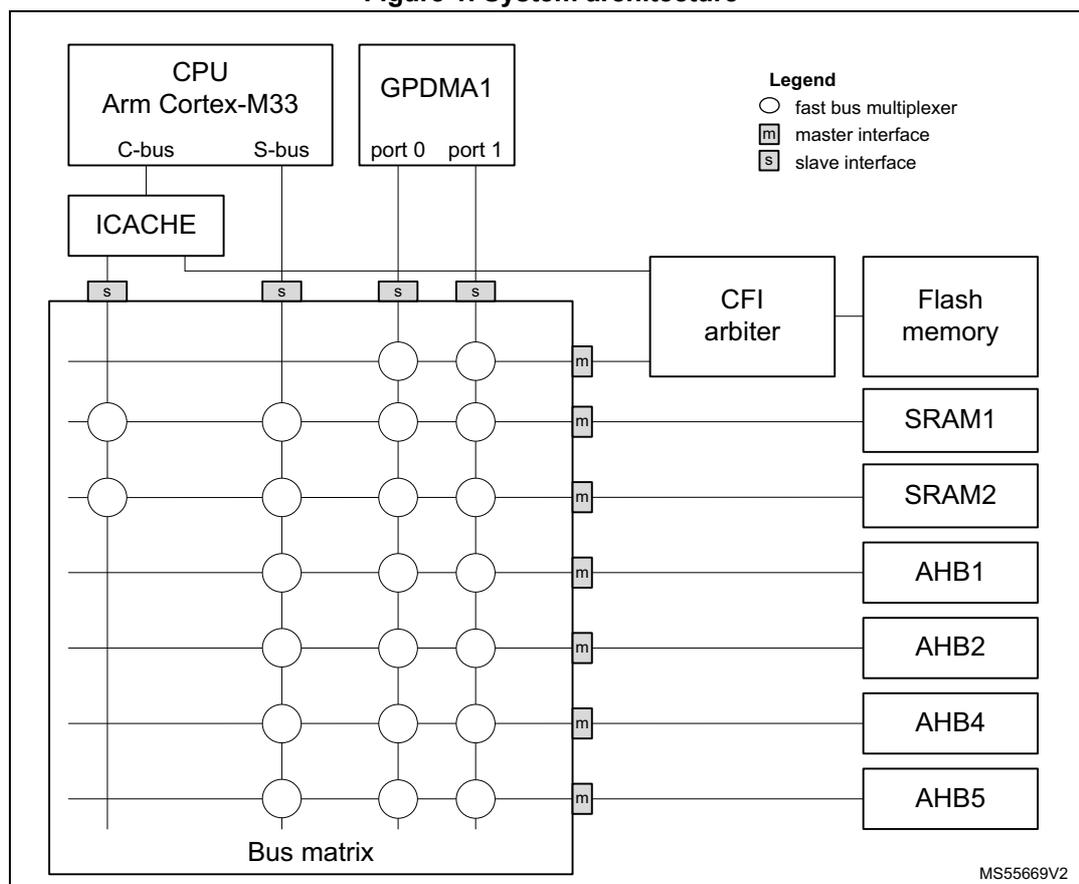
The diagram illustrates the system architecture of the Arm Cortex-M33 CPU. At the top left, the CPU (Arm Cortex-M33) is shown with its C-bus and S-bus. The C-bus connects to the ICACHE, which in turn connects to the Bus matrix via a slave interface (s). The S-bus connects directly to the Bus matrix via a slave interface (s). The GPDMA1 is shown with port 0 and port 1, both connecting to the Bus matrix via slave interfaces (s). The Bus matrix is a central component that connects to various memory and peripheral blocks. On the right side, the Bus matrix connects to the CFI arbiter, Flash memory, SRAM1, SRAM2, AHB1, AHB2, AHB4, and AHB5. The connections are marked with 'm' for master interface and 's' for slave interface. A legend in the top right corner defines the symbols: a circle for a fast bus multiplexer, 'm' for a master interface, and 's' for a slave interface. The diagram is labeled MS55669V2 in the bottom right corner.
2.1.1 CPU C-bus
This bus connects the C-bus of the CPU to the internal flash memory and to the bus matrix via the instruction cache. This bus is used for instruction fetch and data access to the internal memories mapped in code region. This bus targets the internal flash memory and the internal SRAM (SRAM1 and SRAM2) via the ICACHE address remap function.
2.1.2 CPU S-bus
This bus connects the system bus of the CPU to the bus matrix, and it is used by the core to access data located in a peripheral or SRAM area. This bus targets the internal SRAM (SRAM1 and SRAM2), the AHB1 peripherals including the APB1 and APB2 peripherals, AHB2, AHB4 peripherals including the APB7, and AHB5 peripherals.
2.1.3 GPDMA1-bus
The buses connect the two AHB master interfaces of the GPDMA1 to the bus matrix. This targets the internal flash memory, the internal SRAMs (SRAM1, SRAM2), the AHB1 peripherals including the APB1 and APB2 peripherals, the AHB2 peripherals, AHB4 peripherals including the APB7, and AHB5 peripherals.
2.1.4 Bus matrix
The bus matrix manages the access arbitration (based on fixed priority) between masters, and features a bus multiplexer used to connect each master to a given slave without latency.
Table 1. Bus matrix access arbitration
| Master | Priority |
|---|---|
| CPU core S-bus | 1 (highest) |
| ICACHE slow port | 2 |
| GPDMA1 port 0 | 3 |
| GPDMA1 port 1 | 4 (lowest) |
2.1.5 AHB/APB bridges
The three bridges (AHB1 to APB1, AHB1 to APB2, and AHB4 to APB7) provide full synchronous connections between the AHB and the APB buses, resulting in flexible selection of the peripheral frequency.
Refer to Section 2.3.2: Memory map and register boundary addresses for the address mapping of the peripherals connected to these bridges.
After each device reset, the clock of peripherals having an xxEN bit in the RCC is disabled. Before using a peripheral, its clock must be enabled in the RCC_AHBxENR and RCC_APBxENR registers.
Note: When a 16- or 8-bit access is performed on an APB register, the access is transformed into a 32-bit access: the bridge duplicates the 16- or 8-bit data to feed the 32-bit vector.
AHB5 is a semisynchronous bus, connected through a bridge to the bus matrix.
2.2 TrustZone ® security architecture (a)
The security architecture is based on Arm ® TrustZone with the Armv8-M mainline extension.
The TZEN option bit in the FLASH_OPTR register activates TrustZone security.
When the TrustZone is enabled, the SAU (security-attribution unit) and IDAU (implementation-defined-attribution unit) defines the access permissions based on secure and nonsecure states.
- • SAU: up to eight SAU configurable regions are available for security attribution.
- • IDAU: provides a first memory partition as nonsecure or nonsecure callable attributes. The IDAU memory map partition is not configurable and fixed by hardware implementation (refer to Figure 2: Memory map ). It is then combined with the results from the SAU security attribution, and the higher security state is selected.
a. Available only on STM32WBA52/4/5xx devices.
Based on IDAU security attribution, the flash memory, system SRAMs and peripherals memory space are aliased twice for secure and nonsecure states. However, the external memories space is not aliased.
Table 2 shows a typical example of eight SAU regions mapping, based on IDAU regions. The user can split and choose the secure, nonsecure or NSC regions for external memories according to application needs.
Table 2. Memory map security attribution example vs. SAU configuration regions (1)
| Region description | Address range | IDAU security attribution | SAU security attribution typical configuration | Final security attribution |
|---|---|---|---|---|
| Reserved | 0x0000 0000 to 0x07FF FFFF | Nonsecure | Secure, nonsecure or NSC | |
| Code Flash and SRAM | 0x0800 0000 to 0x0BFF FFFF | Nonsecure | Nonsecure | |
| 0x0C00 0000 to 0x0FFF FFFF | NSC | Secure or NSC | ||
| Reserved | 0x1000 0000 to 0x17FF FFFF | Nonsecure | ||
| 0x1800 0000 to 0x1FFF FFFF | ||||
| SRAM | 0x2000 0000 to 0x2FFF FFFF | Nonsecure | ||
| 0x3000 0000 to 0x3FFF FFFF | ||||
| Peripherals | 0x4000 0000 to 0x4FFF FFFF | Nonsecure | Nonsecure | |
| 0x5000 0000 to 0x5FFF FFFF | NSC | Secure or NSC | ||
| Reserved | 0x6000 0000 to 0xDFFF FFFF | Nonsecure | Secure, nonsecure or NSC |
1. NSC = nonsecure callable
2.2.1 Default TrustZone security state
When the TrustZone security is activated by the TZEN option bit in the FLASH_OPTR, the default system security state is detailed below:
- • CPU:
- – CPU1 Cortex-M33 is in secure state after reset. The boot address must point to a secure area.
- • Memory map:
- – SAU is fully secure after reset. Consequently, all memory map is fully secure. Up to height SAU configurable regions are available for security attribution.
- • Flash memory:
- – The flash memory security area is defined by watermark user options.
- – Flash block-based security attributions are nonsecure after reset.
- • SRAMs:
- – All SRAMs are secure after reset. MPCBBx (block-based memory protection controller) are secure.
- • Peripherals (see
Table 3
and
Table 4
for a list of securable and TrustZone-aware peripherals)
- – Securable peripherals are nonsecure after reset.
- – TrustZone-aware peripherals are nonsecure after reset. Their secure configuration registers are secure.
- • All GPIOs are secure after reset.
- • Interrupts:
- – NVIC: All interrupts are secure after reset. NVIC is banked for secure and nonsecure state.
- – TZIC: All illegal access interrupts are disabled after reset (see Section 5.5: GTZC interrupts ).
2.2.2 TrustZone peripheral classification
When the TrustZone security is active, a peripheral can be either securable or TrustZone-aware type as follows:
- • Securable: peripheral protected by an AHB/APB firewall gate controlled from TZSC controller to define security properties
- • TrustZone-aware: peripheral connected directly to AHB or APB bus and implementing a specific TrustZone behavior such as a subset of registers being secure.
Refer to Section 5: Global TrustZone controller (GTZC) for more details.
Table 3 and Table 4 list the securable and TrustZone-aware peripherals within the system.
Table 3. Securable peripherals by TZSC
| Bus | Peripheral |
|---|---|
| AHB5 | 2.4 GHz RADIO + SEQRAM |
| PTACONV (1) | |
| AHB4 | ADC4 |
Table 3. Securable peripherals by TZSC (continued)
| Bus | Peripheral |
|---|---|
| AHB2 | SAES |
| PKA | |
| RNG | |
| HASH | |
| AES | |
| AHB1 | ICACHE registers |
| TSC | |
| CRC | |
| RAMCFG | |
| APB7 | LPTIM1 |
| I2C3 | |
| COMP (1) | |
| LPUART1 | |
| SPI3 | |
| APB2 | TIM17 |
| TIM16 | |
| SAI1 (1) | |
| USART1 | |
| SPI1 | |
| TIM1 | |
| APB1 | LPTIM2 |
| I2C1 | |
| USART2 | |
| IWDG | |
| WWDG | |
| TIM3 | |
| TIM2 |
1. Available only on STM32WBA54/55xx devices.
Table 4. TrustZone-aware peripherals
| Bus | Peripheral |
|---|---|
| AHB4 | EXTI |
| RCC | |
| PWR |
Table 4. TrustZone-aware peripherals (continued)
| Bus | Peripheral |
|---|---|
| AHB2 | HSEM |
| GPIOH | |
| GPIOC | |
| GPIOB | |
| GPIOA | |
| AHB1 | GTZC-MCPBB6 |
| GTZC-MCPBB2 | |
| GTZC-MCPBB1 | |
| GTZC-TZSC | |
| GTZC-TZIC | |
| FLASH interface | |
| GPDMA1 | |
| APB7 | TAMP |
| RTC | |
| SYSCFG |
2.3 Memory organization
2.3.1 Introduction
Program memory, data memory, registers and I/O ports are organized within the same linear 4-Gbyte address space.
The bytes are coded in memory in Little Endian format. The lowest numbered byte in a word is considered the word's least significant byte and the highest numbered byte the most significant.
The addressable memory space is divided into eight main blocks, of 512 Mbytes each.
2.3.2 Memory map and register boundary addresses
Figure 2. Memory map
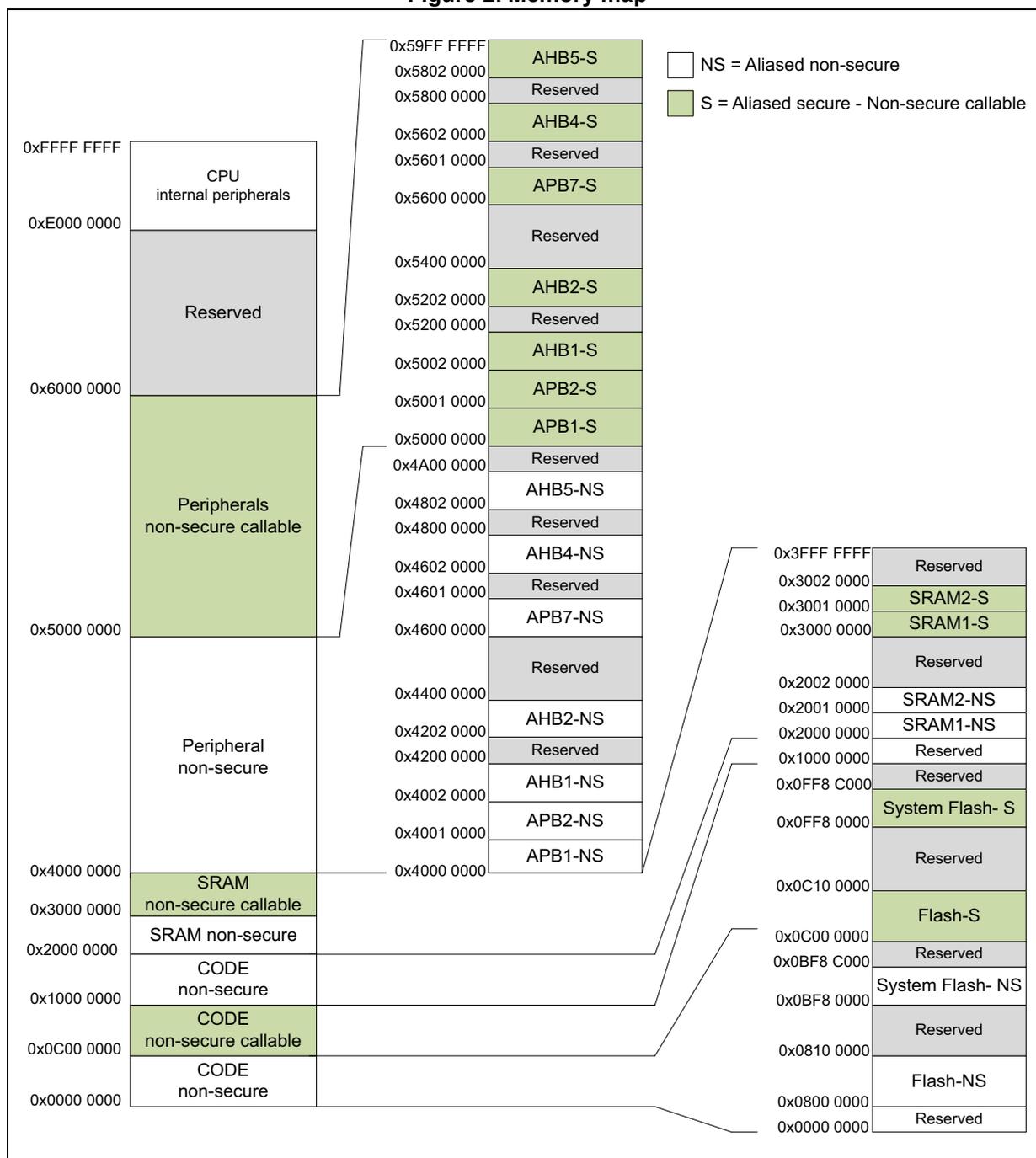
Legend:
- NS = Aliased non-secure
- S = Aliased secure - Non-secure callable
| Address Range | Memory Region / Peripheral | Security Attribute |
|---|---|---|
| 0x0000 0000 - 0x00F0 0000 | CODE non-secure | NS |
| 0x00F0 0000 - 0x00F0 0000 | CODE non-secure callable | S |
| 0x00F0 0000 - 0x0100 0000 | CODE non-secure | NS |
| 0x0100 0000 - 0x0200 0000 | SRAM non-secure | NS |
| 0x0200 0000 - 0x0400 0000 | SRAM non-secure callable | S |
| 0x0400 0000 - 0x4000 0000 | Peripheral non-secure | NS |
| 0x4000 0000 - 0x5000 0000 | Reserved | |
| 0x5000 0000 - 0x6000 0000 | Peripherals non-secure callable | S |
| 0x6000 0000 - 0xE000 0000 | Reserved | |
| 0xE000 0000 - 0xFFFF FFFF | CPU internal peripherals |
| Address Range | Memory Region / Peripheral | Security Attribute |
|---|---|---|
| 0x0000 0000 - 0x0800 0000 | Reserved | |
| 0x0800 0000 - 0x0810 0000 | Flash-NS | NS |
| 0x0810 0000 - 0x0BF8 0000 | Reserved | |
| 0x0BF8 0000 - 0x0BF8 0000 | System Flash- NS | NS |
| 0x0BF8 0000 - 0x0C00 0000 | Reserved | |
| 0x0C00 0000 - 0x0C10 0000 | Flash-S | S |
| 0x0C10 0000 - 0x0FF8 0000 | Reserved | |
| 0x0FF8 0000 - 0x0FF8 0000 | System Flash- S | S |
| 0x0FF8 0000 - 0x1000 0000 | Reserved | |
| 0x1000 0000 - 0x2000 0000 | SRAM1-NS | NS |
| 0x2000 0000 - 0x2001 0000 | SRAM2-NS | NS |
| 0x2001 0000 - 0x2002 0000 | SRAM2-S | S |
| 0x2002 0000 - 0x3000 0000 | Reserved | |
| 0x3000 0000 - 0x3000 0000 | SRAM1-S | S |
| 0x3000 0000 - 0x3001 0000 | SRAM2-S | S |
| 0x3001 0000 - 0x3002 0000 | Reserved | |
| 0x3002 0000 - 0x3FFF FFFF | Reserved |
| Address Range | Memory Region / Peripheral | Security Attribute |
|---|---|---|
| 0x4000 0000 - 0x4001 0000 | APB1-NS | NS |
| 0x4001 0000 - 0x4002 0000 | APB2-NS | NS |
| 0x4002 0000 - 0x4200 0000 | Reserved | |
| 0x4200 0000 - 0x4202 0000 | AHB1-NS | NS |
| 0x4202 0000 - 0x4400 0000 | Reserved | |
| 0x4400 0000 - 0x4600 0000 | APB7-NS | NS |
| 0x4600 0000 - 0x4601 0000 | Reserved | |
| 0x4601 0000 - 0x4800 0000 | Reserved | |
| 0x4800 0000 - 0x4802 0000 | AHB4-NS | NS |
| 0x4802 0000 - 0x4A00 0000 | Reserved | |
| 0x4A00 0000 - 0x5000 0000 | Reserved | |
| 0x5000 0000 - 0x5001 0000 | APB1-S | S |
| 0x5001 0000 - 0x5002 0000 | APB2-S | S |
| 0x5002 0000 - 0x5200 0000 | Reserved | |
| 0x5200 0000 - 0x5202 0000 | AHB1-S | S |
| 0x5202 0000 - 0x5400 0000 | Reserved | |
| 0x5400 0000 - 0x5600 0000 | APB7-S | S |
| 0x5600 0000 - 0x5601 0000 | Reserved | |
| 0x5601 0000 - 0x5800 0000 | Reserved | |
| 0x5800 0000 - 0x5802 0000 | Reserved | |
| 0x5802 0000 - 0x59FF FFFF | Reserved |
STM32WBA52/54/55xG devices contain a 1-Mbyte flash memory from address offset 0x00 0000 to 0x0F FFFF, and SRAM1 64-Kbyte from address offset 0x0 0000 to 0x0 FFFF. (continuous SRAM space with SRAM2).
STM32WBA52/54/55xE devices contain a 512-Kbyte flash memory from address offset 0x00 0000 to 0x07 FFFF, and SRAM1 32-Kbyte from address offset 0x0 0000 to 0x0 7FFF (non-continuous SRAM space with SRAM2).
STM32WBA50xG devices contain a 1-Mbyte flash memory from address offset 0x00 000 to 0x0F FFFF, SRAM1 16-Kbyte from address offset 0x0 0000 to 0x0 3FFF (non-continuous SRAM space with SRAM2), and SRAM2 48-Kbyte from address offset 0x1 0000 to 0x1 BFFF.
Any memory area not allocated to on-chip memories and peripherals is considered “Reserved”.
Table 5 gives the boundary addresses of the peripherals available in the device.
Table 5. Memory map and peripheral register boundary addresses
| Bus | Nonsecure callable boundary address (1) | Nonsecure boundary address (1) | Size (bytes) | Peripheral | Peripheral register map |
|---|---|---|---|---|---|
| - | 0x5A00 0000 - 0xDFFF FFFF | 0x4A00 0000 - 0x4FFF FFFF | - | Reserved | - |
| AHB5 | 0x5803 8400 - 0x59FF FFFF | 0x4803 8400 - 0x49FF FFFF | - | Reserved | - |
| 0x5803 8000 - 0x5803 83FF | 0x4803 8000 - 0x4803 83FF | 1 K | PTACONV (2) | Section 10.5.4 on page 272 | |
| 0x5802 C000 - 0x5803 7FFF | 0x4802 C000 - 0x4803 7FFF | - | Reserved | - | |
| 0x5802 8000 - 0x5802 BFFF | 0x4802 8000 - 0x4802 BFFF | 16 K | RXTXRAM | Section 6.6.11 on page 175 | |
| 0x5802 1200 - 0x5802 7FFF | 0x4802 1200 - 0x4802 7FFF | - | Reserved | - | |
| 0x5802 1000 - 0x5802 11FF | 0x4802 1000 - 0x4802 11FF | 0.5 K | SEQRAM | Section 6.6.11 on page 175 | |
| 0x5802 0000 - 0x5802 0FFF | 0x4802 0000 - 0x4802 0FFF | 4 K | 2.4 GHz RADIO | - | |
| 0x5800 0000 - 0x5801 FFFF | 0x4800 0000 - 0x4801 FFFF | - | Reserved | - | |
| AHB4 | 0x5602 2400 - 0x57FF FFFF | 0x4602 2400 - 0x47FF FFFF | - | Reserved | - |
| 0x5602 2000 - 0x5602 23FF | 0x4602 2000 - 0x4602 23FF | 1 K | EXTI | Section 19.6.15 on page 615 | |
| 0x5602 1400 - 0x5602 1FFF | 0x4602 1400 - 0x4602 1FFF | - | Reserved | - | |
| 0x5602 1000 - 0x5602 13FF | 0x4602 1000 - 0x4602 13FF | 1 K | ADC4 | Section 21.7.18 on page 684 | |
| 0x5602 0C00 - 0x5602 0FFF | 0x4602 0C00 - 0x4602 0FFF | 1 K | RCC | Section 12.8.54 on page 429 | |
| 0x5602 0800 - 0x5602 0BFF | 0x4602 0800 - 0x4602 0BFF | 1 K | PWR | Section 11.10.25 on page 328 | |
| 0x5602 0000 - 0x5602 07FF | 0x4602 0000 - 0x4602 07FF | - | Reserved | - | |
| - | 0x5601 0000 - 0x5601 FFFF | 0x4601 0000 - 0x4601 FFFF | - | Reserved | - |
Table 5. Memory map and peripheral register boundary addresses (continued)
| Bus | Nonsecure callable boundary address (1) | Nonsecure boundary address (1) | Size (bytes) | Peripheral | Peripheral register map |
|---|---|---|---|---|---|
| APB7 | 0x5600 8000 - 0x5600 FFFF | 0x4600 8000 - 0x4600 FFFF | - | Reserved | - |
| 0x5600 7C00 - 0x5600 7FFF | 0x4600 7C00 - 0x4600 7FFF | 1 K | TAMP | ||
| 0x5600 7800 - 0x5600 7BFF | 0x4600 7800 - 0x4600 7BFF | 1 K | RTC | ||
| 0x5600 5800 - 0x5600 77FF | 0x4600 5800 - 0x4600 77FF | - | Reserved | - | |
| 0x5600 5400 - 0x5600 57FF | 0x4600 5400 - 0x4600 57FF | 1 K | COMP (2) | ||
| 0x5600 4800 - 0x5600 53FF | 0x4600 4800 - 0x4600 53FF | - | Reserved | - | |
| 0x5600 4400 - 0x5600 47FF | 0x4600 4400 - 0x4600 47FF | 1 K | LPTIM1 | Section 32.7.16 on page 1257 | |
| 0x5600 2C00 - 0x5600 43FF | 0x4600 2C00 - 0x4600 43FF | - | Reserved | - | |
| 0x5600 2800 - 0x5600 2BFF | 0x4600 2800 - 0x4600 2BFF | 1 K | I2C3 | Section 38.9.13 on page 1449 | |
| 0x5600 2400 - 0x5600 27FF | 0x4600 2400 - 0x4600 27FF | 1 K | LPUART1 | Section 40.7.15 on page 1593 | |
| 0x5600 2000 - 0x5600 23FF | 0x4600 2000 - 0x4600 23FF | 1 K | SPI3 | Section 41.8.15 on page 1647 | |
| 0x5600 0800 - 0x5600 1FFF | 0x4600 0800 - 0x4600 1FFF | - | Reserved | - | |
| 0x5600 0400 - 0x5600 07FF | 0x4600 0400 - 0x4600 07FF | 1 K | SYSCFG | Section 15.3.12 on page 517 | |
| 0x5600 0000 - 0x5600 03FF | 0x4600 0000 - 0x4600 03FF | - | Reserved | - | |
| - | 0x5400 0000 - 0x55FF FFFF | 0x4400 0000 - 0x45FF FFFF | - | Reserved | - |
| AHB2 | 0x520C 4000 - 0x53FF FFFF | 0x420C 4000 - 0x43FF FFFF | - | Reserved | - |
| 0x520C 3400 - 0x520C 3FFF | 0x420C 3400 - 0x420C 3FFF | 8 K | PKA continue | Section 28.7.5 on page 888 | |
| 0x520C 2400 - 0x520C 33FF | 0x420C 2400 - 0x420C 33FF | PKA RAM | |||
| 0x520C 2000 - 0x520C 23FF | 0x420C 2000 - 0x420C 23FF | PKA | |||
| 0x520C 1C00 - 0x520C 1FFF | 0x420C 1C00 - 0x420C 1FFF | 1 K | HSEM | Section 13.4.15 on page 455 | |
| 0x520C 1000 - 0x520C 1BFF | 0x420C 1000 - 0x420C 1BFF | - | Reserved | - | |
| 0x520C 0C00 - 0x520C 0FFF | 0x420C 0C00 - 0x420C 0FFF | 1 K | SAES (3) | Section 26.8.21 on page 832 | |
| 0x520C 0800 - 0x520C 0BFF | 0x420C 0800 - 0x420C 0BFF | 1 K | RNG | Section 24.7.6 on page 732 | |
| 0x520C 0400 - 0x520C 07FF | 0x420C 0400 - 0x420C 07FF | 1 K | HASH | Section 27.6.8 on page 854 | |
| 0x520C 0000 - 0x520C 03FF | 0x420C 0000 - 0x420C 03FF | 1 K | AES | Section 25.8.21 on page 776 | |
| 0x5202 2000 - 0x520B FFFF | 0x4202 2000 - 0x420B FFFF | - | Reserved | - | |
| 0x5202 1C00 - 0x5202 1FFF | 0x4202 1C00 - 0x4202 1FFF | 1 K | GPIOH | Section 14.8.15 on page 502 | |
| 0x5202 0C00 - 0x5202 1BFF | 0x4202 0C00 - 0x4202 1BFF | - | Reserved | - | |
| 0x5202 0800 - 0x5202 0BFF | 0x4202 0800 - 0x4202 0BFF | 1 K | GPIOC | Section 14.8.14 on page 501 | |
| 0x5202 0400 - 0x5202 07FF | 0x4202 0400 - 0x4202 07FF | 1 K | GPIOB | Section 14.8.13 on page 499 | |
| 0x5202 0000 - 0x5202 03FF | 0x4202 0000 - 0x4202 03FF | 1 K | GPIOA | Section 14.8.12 on page 497 | |
| - | 0x5200 0000 - 0x5201 FFFF | 0x4200 0000 - 0x4201 FFFF | - | Reserved | - |
Table 5. Memory map and peripheral register boundary addresses (continued)
| Bus | Nonsecure callable boundary address (1) | Nonsecure boundary address (1) | Size (bytes) | Peripheral | Peripheral register map |
|---|---|---|---|---|---|
| AHB1 | 0x5003 4400 - 0x51FF FFFF | 0x4003 4400 - 0x41FF FFFF | - | Reserved | - |
| 0x5003 4000 - 0x5003 43FF | 0x4003 4000 - 0x4003 43FF | 1 K | GTZC_MPCBB6 (3) | Section 5.8.6 on page 164 | |
| 0x5003 3400 - 0x5003 3FFF | 0x4003 3400 - 0x4003 3FFF | - | Reserved | - | |
| 0x5003 3000 - 0x5003 33FF | 0x4003 3000 - 0x4003 33FF | 1 K | GTZC_MPCBB2 (3) | Section 5.8.5 on page 163 | |
| 0x5003 2C00 - 0x5003 2FFF | 0x4003 2C00 - 0x4003 2FFF | 1 K | GTZC_MPCBB1 (3) | ||
| 0x5003 2800 - 0x5003 2BFF | 0x4003 2800 - 0x4003 2BFF | 1 K | GTZC_TZIC (3) | Section 5.7.13 on page 159 | |
| 0x5003 2400 - 0x5003 27FF | 0x4003 2400 - 0x4003 27FF | 1 K | GTZC_TZSC (3) | Section 5.6.8 on page 141 | |
| 0x5003 0800 - 0x5003 23FF | 0x4003 0800 - 0x4003 23FF | - | Reserved | - | |
| 0x5003 0400 - 0x5003 07FF | 0x4003 0400 - 0x4003 07FF | 1 K | ICACHE | Section 8.7.8 on page 257 | |
| 0x5002 7000 - 0x5003 03FF | 0x4002 7000 - 0x4003 03FF | - | Reserved | - | |
| 0x5002 6000 - 0x5002 6FFF | 0x4002 6000 - 0x4002 6FFF | 4 K | RAMCFG | Section 6.6.11 on page 175 | |
| 0x5002 4400 - 0x5002 5FFF | 0x4002 4400 - 0x4002 5FFF | - | Reserved | - | |
| 0x5002 4000 - 0x5002 43FF | 0x4002 4000 - 0x4002 43FF | 1 K | TSC | Section 23.6.11 on page 714 | |
| 0x5002 3400 - 0x5002 3FFF | 0x4002 3400 - 0x4002 3FFF | - | Reserved | - | |
| 0x5002 3000 - 0x5002 33FF | 0x4002 3000 - 0x4002 33FF | 1 K | CRC | Section 20.4.6 on page 623 | |
| 0x5002 2400 - 0x5002 2FFF | 0x4002 2400 - 0x4002 2FFF | - | Reserved | - | |
| 0x5002 2000 - 0x5002 23FF | 0x4002 2000 - 0x4002 23FF | 1 K | FLASH interface | Section 7.9.30 on page 237 | |
| 0x5002 1000 - 0x5002 1FFF | 0x4002 1000 - 0x4002 1FFF | - | Reserved | - | |
| 0x5002 0000 - 0x5002 0FFF | 0x4002 0000 - 0x4002 0FFF | 4 K | GPDMA1 | Section 17.8.16 on page 589 | |
| APB2 | 0x5001 5800 - 0x5001 FFFF | 0x4001 5800 - 0x4001 FFFF | - | Reserved | - |
| 0x5001 5400 - 0x5001 57FF | 0x4001 5400 - 0x4001 57FF | 1 K | SAI1 (2) | ||
| 0x5001 4C00 - 0x5001 53FF | 0x4001 4C00 - 0x4001 53FF | - | Reserved | - | |
| 0x5001 4800 - 0x5001 4BFF | 0x4001 4800 - 0x4001 4BFF | 1 K | TIM17 (3) | Section 31.6.22 on page 1211 | |
| 0x5001 4400 - 0x5001 47FF | 0x4001 4400 - 0x4001 47FF | 1 K | TIM16 | Section 31.6.22 on page 1211 | |
| 0x5001 3C00 - 0x5001 43FF | 0x4001 3C00 - 0x4001 43FF | - | Reserved | - | |
| 0x5001 3800 - 0x5001 3BFF | 0x4001 3800 - 0x4001 3BFF | 1 K | USART1 | Section 39.8.17 on page 1538 | |
| 0x5001 3400 - 0x5001 37FF | 0x4001 3400 - 0x4001 37FF | - | Reserved | - | |
| 0x5001 3000 - 0x5001 33FF | 0x4001 3000 - 0x4001 33FF | 1 K | SPI1 (3) | Section 41.8.15 on page 1647 | |
| 0x5001 2C00 - 0x5001 2FFF | 0x4001 2C00 - 0x4001 2FFF | 1 K | TIM1 | Section 29.6.31 on page 1029 | |
| 0x5001 0000 - 0x5001 2BFF | 0x4001 0000 - 0x4001 2BFF | - | Reserved | - |
Table 5. Memory map and peripheral register boundary addresses (continued)
| Bus | Nonsecure callable boundary address (1) | Nonsecure boundary address (1) | Size (bytes) | Peripheral | Peripheral register map |
|---|---|---|---|---|---|
| APB1 | 0x5000 9800 - 0x5000 FFFF | 0x4000 9800 - 0x4000 FFFF | - | Reserved | - |
| 0x5000 9400 - 0x5000 97FF | 0x4000 9400 - 0x4000 97FF | 1 K | LPTIM2 (3) | Section 32.7.16 on page 1257 | |
| 0x5000 5800 - 0x5000 93FF | 0x4000 5800 - 0x4000 93FF | - | Reserved | - | |
| 0x5000 5400 - 0x5000 57FF | 0x4000 5400 - 0x4000 57FF | 1 K | I2C1 (3) | Section 38.9.13 on page 1449 | |
| 0x5000 4800 - 0x5000 53FF | 0x4000 4800 - 0x4000 53FF | - | Reserved | - | |
| 0x5000 4400 - 0x5000 47FF | 0x4000 4400 - 0x4000 47FF | 1 K | USART2 (3) | Section 39.8.17 on page 1538 | |
| 0x5000 3400 - 0x5000 43FF | 0x4000 3400 - 0x4000 43FF | - | Reserved | - | |
| 0x5000 3000 - 0x5000 33FF | 0x4000 3000 - 0x4000 33FF | 1 K | IWDG | Section 34.7.7 on page 1275 | |
| 0x5000 2C00 - 0x5000 2FFF | 0x4000 2C00 - 0x4000 2FFF | 1 K | WWDG | Section 35.6.4 on page 1282 | |
| 0x5000 0800 - 0x5000 2BFF | 0x4000 0800 - 0x4000 2BFF | - | Reserved | - | |
| 0x5000 0400 - 0x5000 07FF | 0x4000 0400 - 0x4000 07FF | 1 K | TIM3 (3) | Section 30.5.31 on page 1145 | |
| 0x5000 0000 - 0x5000 03FF | 0x4000 0000 - 0x4000 03FF | 1 K | TIM2 | Section 30.5.31 on page 1145 | |
| AHB | 0x3002 0000 - 0x4FFF FFFF | 0x2002 0000 - 0x3FFF FFFF | - | Reserved | - |
| 0x3001 0000 - 0x3001 FFFF | 0x2001 0000 - 0x2001 FFFF | 64 K (4) | SRAM2 | - | |
| 0x3000 0000 - 0x3000 FFFF | 0x2000 0000 - 0x2000 FFFF | 64 K (5) | SRAM1 | - | |
| 0x0FF9 8000 - 0x2FFF FFFF | 0x0FF9 8000 - 0x1FFF FFFF | - | Reserved | - | |
| 0x0FF9 4000 - 0x0FF9 7FFF | 0x0BF9 4000 - 0x0BF9 7FFF | 16 K | Flash user options | Section 7.9.30 on page 237 | |
| 0x0FF9 0500 - 0x0FF9 3FFF | 0x0BF9 0500 - 0x0BF9 3FFF | 14.75 K | DESIG | Section 44.1.13 on page 1839 | |
| 0x0FF9 0200 - 0x0FF9 04FF | 0x0BF9 0200 - 0x0BF9 04FF | - | Reserved | - | |
| 0x0FF9 0000 - 0x0FF9 01FF | 0x0BF9 0000 - 0x0BF9 01FF | 512 | OTP | - | |
| 0x0FF8 8000 - 0x0FF8 FFFF | 0x0BF8 8000 - 0x0BF8 FFFF | 32 K | Bootloader | - | |
| 0x0FF8 6000 - 0x0FF8 7FFF | 0x0BF8 6000 - 0x0BF8 7FFF | 8 K | RSS-Lib (3) | - | |
| 0x0FF8 0000 - 0x0FF8 5FFF | 0x0BF8 0000 - 0x0BF8 5FFF | 24 K | RSS-Boot (3) | - | |
| 0x0C10 0000 - 0x0FF7 FFFF | 0x0810 0000 - 0x0BF7 FFFF | - | Reserved | - | |
| 0x0C00 0000 - 0x0C0F FFFF | 0x0800 0000 - 0x080F FFFF | 1 M (6) | User flash | - | |
| 0x0000 0000 - 0x0BFF FFFF | 0x0000 0000 - 0x07FF FFFF | - | Reserved | - |
1. Gray shaded fields are reserved.
2. Available only on STM32WBA54/5xx devices.
3. Available only on STM32WBA52/54/55xx devices.
4. Device-dependent (STM32WBA52/54/55xx 64-Kbyte SRAM2 offset 0x1 0000 - 0x1 FFFF, STM32WBA50xG 48-Kbyte SRAM2 offset 0x1 0000 - 0x1 BFFF, where 0x1 C000 - 0x1 FFFF is reserved).
5. Device-dependent (STM32WBA52/54/55xG 64-Kbyte SRAM1 offset 0x0 0000 - 0x0 FFFF, STM32WBA52/4/5xE 32-Kbyte SRAM1 offset 0x0 0000 - 0x0 7FFF, where 0x0 8000 - 0x0 FFFF is reserved, STM32WBA50xx 16-Kbyte SRAM1 offset 0x0 0000 - 0x0 3FFF, where 0x0 4000 - 0x0 FFFF is reserved).
6. Device-dependent (STM32WBA5xxG 1-Mbyte User flash offset 0x00 0000 - 0x0F FFFF, STM32WBA5xxE 512-Kbyte user flash offset 0x00 0000 - 0x07 FFFF, where 0x08 0000 - 0x0F FFFF is reserved).
2.3.3 Embedded SRAM
The devices feature up to 128-Kbyte SRAMs:
- • SRAM1 up to 64-Kbyte (STM32WBA52/54/55xG 64-Kbyte, STM32WBA52/54/55xE 32-Kbyte, STM32WBA50xG 16-Kbyte)
- • SRAM2 up to 64-Kbyte (STM32WBA52/54/55xx 64-Kbyte, STM32WBA50xG 48-Kbyte)
These SRAMs can be accessed as bytes, half-words (16 bits) or full words (32 bits). These memories can be addressed both by CPU and DMA.
The CPU can access the SRAM1, and SRAM2 through the system bus or, when remapped in the I-CACHE, through the C-bus, depending on the selected address.
When TrustZone security is enabled, all SRAMs are secure after reset. The SRAM can be programmed as nonsecure with a block granularity. For more details, refer to Section 5: Global TrustZone® controller (GTZC) .
SRAM features are detailed in Section 6.3.1: Internal SRAMs features .
2.3.4 Flash memory overview
The flash memory is composed of two distinct physical areas:
- • The main flash memory block, that contains the application program and user data.
- • The information block, that is composed of the following parts:
- – option bytes for hardware and memory protection user configuration
- – system memory that contains ST proprietary code
- – OTP (one-time programmable) area
The flash interface implements instruction access and data access based on the AHB protocol. It also implements the logic necessary to carry out the memory operations (program/erase) controlled through the FLASH registers, plus the security access control features. Refer to Section 7: Embedded flash memory (FLASH) for more details.