30. Debug support (DBG)
30.1 Overview
The STM32C0 series devices are built around a Cortex ® -M0+ core which contains hardware extensions for advanced debugging features. The debug extensions allow the core to be stopped either on a given instruction fetch (breakpoint) or data access (watchpoint). When stopped, the core's internal state and the system's external state may be examined. Once examination is complete, the core and the system may be restored and program execution resumed.
The debug features are used by the debugger host when connecting to and debugging the STM32C0 series MCUs.
One interface for debug is available:
- • Serial wire
Figure 328. Block diagram of STM32C0 series MCU and Cortex ® -M0+-level debug support
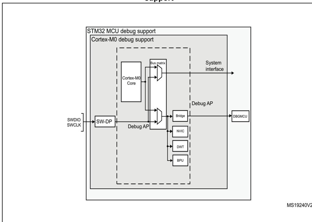
The diagram illustrates the internal architecture of the STM32C0 series MCU, focusing on the debug support system. At the top, a box labeled 'STM32 MCU debug support' contains a dashed box labeled 'Cortex-M0 debug support'. Inside this dashed box, a 'Cortex-M0 Core' is connected to a 'Bus matrix'. The 'Bus matrix' has multiple output paths: one labeled 'System interface' pointing out to the right, and another pointing down to a 'Debug AP' block. Below the 'Debug AP' block, there are four stacked blocks: 'Bridge', 'NVIC', 'DWT', and 'BPU'. These four blocks are connected to a 'DBGMCU' block located outside the dashed box on the right. On the left side of the 'Cortex-M0 debug support' dashed box, there is an 'SW-DP' block. This block is connected to two external pins labeled 'SWDIO' and 'SWCLK'. The 'SW-DP' block is also connected to the 'Bus matrix' and the 'Debug AP' block. The reference code 'MS19240V2' is located in the bottom right corner of the diagram area.
1. The debug features embedded in the Cortex ® -M0+ core are a subset of the Arm CoreSight Design Kit.
The Arm Cortex ® -M0+ core provides integrated on-chip debug support. It is comprised of:
- • SW-DP: Serial wire
- • BPU: Break point unit
- • DWT: Data watchpoint trigger
It also includes debug features dedicated to the STM32C0 series:
- • Flexible debug pinout assignment
- • MCU debug box (support for low-power modes, control over peripheral clocks, etc.)
Note: For further information on debug functionality supported by the Arm Cortex ® -M0+ core, refer to the Cortex ® -M0+ Technical Reference Manual (see Section 30.2: Reference Arm documentation ).
30.2 Reference Arm documentation
- • Cortex ® -M0+ Technical Reference Manual (TRM), available from http://infocenter.arm.com
- • Arm Debug Interface V5
- • Arm CoreSight Design Kit revision r1p1 Technical Reference Manual
30.3 Pinout and debug port pins
The STM32C0 series MCUs are available in various packages with different numbers of available pins.
30.3.1 SWD port pins
Two pins are used as outputs for the SW-DP as alternate functions of general purpose I/Os. These pins are available on all packages.
Table 170. SW debug port pins
| SW-DP pin name | SW debug port | Pin assignment | |
|---|---|---|---|
| Type | Debug assignment | ||
| SWDIO | I/O | Serial Wire Data Input/Output | PA13 |
| SWCLK | I | Serial Wire Clock | PA14 |
30.3.2 SW-DP pin assignment
After reset (SYSRESETn or PORESETn), the pins used for the SW-DP are assigned as dedicated pins which are immediately usable by the debugger host.
However, the MCU offers the possibility to disable the SWD port and can then release the associated pins for general-purpose I/O (GPIO) usage. For more details on how to disable SW-DP port pins, refer to Section 8.3.2: I/O pin alternate function multiplexer and mapping on page 180 .
30.3.3 Internal pull-up & pull-down on SWD pins
Once the SW I/O is released by the user software, the GPIO controller takes control of these pins. The reset states of the GPIO control registers put the I/Os in the equivalent states:
- • SWDIO: input pull-up
- • SWCLK: input pull-down
Having embedded pull-up and pull-down resistors removes the need to add external resistors.
30.4 ID codes and locking mechanism
There are several ID codes inside the MCU. ST strongly recommends the tool manufacturers (for example Keil, IAR, Raisonance) to lock their debugger using the MCU device ID located at address 0x40015800.
Only the DEV_ID[15:0] should be used for identification by the debugger/programmer tools (the revision ID must not be taken into account).
30.5 SWD port
30.5.1 SWD protocol introduction
This synchronous serial protocol uses two pins:
- • SWCLK: clock from host to target
- • SWDIO: bidirectional
The protocol allows two banks of registers (DPACC registers and APACC registers) to be read and written to.
Bits are transferred LSB-first on the wire.
For SWDIO bidirectional management, the line must be pulled-up on the board (100 k \( \Omega \) recommended by Arm).
Each time the direction of SWDIO changes in the protocol, a turnaround time is inserted where the line is not driven by the host nor the target. By default, this turnaround time is one bit time, however this can be adjusted by configuring the SWCLK frequency.
30.5.2 SWD protocol sequence
Each sequence consist of three phases:
- 1. Packet request (8 bits) transmitted by the host
- 2. Acknowledge response (3 bits) transmitted by the target
- 3. Data transfer phase (33 bits) transmitted by the host or the target
| Bit | Name | Description |
|---|---|---|
| 0 | Start | Must be “1” |
| 1 | APnDP | 0: DP Access 1: AP Access |
| 2 | RnW | 0: Write Request 1: Read Request |
| 4:3 | A[3:2] | Address field of the DP or AP registers (refer to Table 175 on page 1006 ) |
| 5 | Parity | Single bit parity of preceding bits |
| 6 | Stop | 0 |
| 7 | Park | Not driven by the host. Must be read as “1” by the target because of the pull-up |
Refer to the Cortex ® -M0+ TRM for a detailed description of DPACC and APACC registers.
The packet request is always followed by the turnaround time (default 1 bit) where neither the host nor target drive the line.
Table 172. ACK response (3 bits)| Bit | Name | Description |
|---|---|---|
| 0..2 | ACK | 001: FAULT 010: WAIT 100: OK |
The ACK Response must be followed by a turnaround time only if it is a READ transaction or if a WAIT or FAULT acknowledge has been received.
Table 173. DATA transfer (33 bits)| Bit | Name | Description |
|---|---|---|
| 0..31 | WDATA or RDATA | Write or Read data |
| 32 | Parity | Single parity of the 32 data bits |
The DATA transfer must be followed by a turnaround time only if it is a READ transaction.
30.5.3 SW-DP state machine (reset, idle states, ID code)
The State Machine of the SW-DP has an internal ID code which identifies the SW-DP. It follows the JEP-106 standard. This ID code is the default Arm one and is set to 0x0BC1 1477 (corresponding to Cortex ® -M0+).
Note: Note that the SW-DP state machine is inactive until the target reads this ID code.
- • The SW-DP state machine is in RESET STATE either after power-on reset, or after the line is high for more than 50 cycles
- • The SW-DP state machine is in IDLE STATE if the line is low for at least two cycles after RESET state.
- • After RESET state, it is mandatory to first enter into an IDLE state AND to perform a READ access of the DP-SW ID CODE register. Otherwise, the target issues a FAULT acknowledge response on another transactions.
Further details of the SW-DP state machine can be found in the Cortex®-M0+ TRM and the CoreSight Design Kit r1p0 TRM .
30.5.4 DP and AP read/write accesses
- • Read accesses to the DP are not posted: the target response can be immediate (if ACK=OK) or can be delayed (if ACK=WAIT).
- • Read accesses to the AP are posted. This means that the result of the access is returned on the next transfer. If the next access to be done is NOT an AP access, then the DP-RDBUFF register must be read to obtain the result.
The READOK flag of the DP-CTRL/STAT register is updated on every AP read access or RDBUFF read request to know if the AP read access was successful. - • The SW-DP implements a write buffer (for both DP or AP writes), that enables it to accept a write operation even when other transactions are still outstanding. If the write buffer is full, the target acknowledge response is “WAIT”. With the exception of IDCODE read or CTRL/STAT read or ABORT write which are accepted even if the write buffer is full.
- • Because of the asynchronous clock domains SWCLK and HCLK, two extra SWCLK cycles are needed after a write transaction (after the parity bit) to make the write effective internally. These cycles should be applied while driving the line low (IDLE state)
This is particularly important when writing the CTRL/STAT for a power-on request. If the next transaction (requiring a power-on) occurs immediately, it fails.
30.5.5 SW-DP registers
Access to these registers are initiated when APnDP=0
Table 174. SW-DP registers
| A[3:2] | R/W | CTRLSEL bit of SELECT register | Register | Notes |
|---|---|---|---|---|
| 00 | Read | IDCODE | The manufacturer code is set to the default Arm code for Cortex®-M0+: 0x0BC11477 (identifies the SW-DP) | |
| 00 | Write | ABORT |
Table 174. SW-DP registers (continued)
| A[3:2] | R/W | CTRLSEL bit of SELECT register | Register | Notes |
|---|---|---|---|---|
| 01 | Read/Write | 0 | DP-CTRL/STAT | Purpose is to: – request a system or debug power-on – configure the transfer operation for AP accesses – control the pushed compare and pushed verify operations. – read some status flags (overrun, power-on acknowledges) |
| 01 | Read/Write | 1 | WIRE CONTROL | Purpose is to configure the physical serial port protocol (like the duration of the turnaround time) |
| 10 | Read | READ RESEND | Enables recovery of the read data from a corrupted debugger transfer, without repeating the original AP transfer. | |
| 10 | Write | SELECT | The purpose is to select the current access port and the active 4-words register window | |
| 11 | Read/Write | READ BUFFER | This read buffer is useful because AP accesses are posted (the result of a read AP request is available on the next AP transaction). This read buffer captures data from the AP, presented as the result of a previous read, without initiating a new transaction |
30.5.6 SW-AP registers
Access to these registers are initiated when APnDP=1
There are many AP Registers addressed as the combination of:
- • The shifted value A[3:2]
- • The current value of the DP SELECT register.
Table 175. 32-bit debug port registers addressed through the shifted value A[3:2]
| Address | A[3:2] value | Description |
|---|---|---|
| 0x0 | 00 | Reserved, must be kept at reset value. |
| 0x4 | 01 | DP CTRL/STAT register. Used to: – Request a system or debug power-on – Configure the transfer operation for AP accesses – Control the pushed compare and pushed verify operations. – Read some status flags (overrun, power-on acknowledges) |
| Address | A[3:2] value | Description |
|---|---|---|
| 0x8 | 10 | DP SELECT register: Used to select the current access port and the active 4-words register window.
|
| 0xC | 11 | DP RDBUFF register: Used to allow the debugger to get the final result after a sequence of operations (without requesting new JTAG-DP operation) |
30.6 Core debug
Core debug is accessed through the core debug registers. Debug access to these registers is by means of the debug access port. It consists of four registers:
Table 176. Core debug registers| Register | Description |
|---|---|
| DHCSR | The 32-bit Debug Halting Control and Status Register This provides status information about the state of the processor enable core debug halt and step the processor |
| DCRSR | The 17-bit Debug Core Register Selector Register: This selects the processor register to transfer data to or from. |
| DCRDR | The 32-bit Debug Core Register Data Register: This holds data for reading and writing registers to and from the processor selected by the DCRSR (Selector) register. |
| DEMCR | The 32-bit Debug Exception and Monitor Control Register: This provides Vector Catching and Debug Monitor Control. |
These registers are not reset by a system reset. They are only reset by a power-on reset. Refer to the Cortex®-M0+ TRM for further details.
To Halt on reset, it is necessary to:
- • enable the bit0 (VC_CORRESET) of the Debug and Exception Monitor Control Register
- • enable the bit0 (C_DEBUGEN) of the Debug Halting Control and Status Register
30.7 BPU (break point unit)
The Cortex®-M0+ BPU implementation provides four breakpoint registers. The BPU is a subset of the Flash Patch and Breakpoint (FPB) block available in Armv7-M (Cortex-M3 & Cortex-M4).
30.7.1 BPU functionality
The processor breakpoints implement PC based breakpoint functionality.
Refer the Armv6-M Arm and the Arm CoreSight Components Technical Reference Manual for more information about the BPU CoreSight identification registers, and their addresses and access types.
30.8 DWT (data watchpoint)
The Cortex ® -M0+ DWT implementation provides two watchpoint register sets.
30.8.1 DWT functionality
The processor watchpoints implement both data address and PC based watchpoint functionality, a PC sampling register, and support comparator address masking, as described in the Armv6-M Arm .
30.8.2 DWT Program counter sample register
A processor that implements the data watchpoint unit also implements the Armv6-M optional DWT Program Counter Sample Register (DWT_PCSR). This register permits a debugger to periodically sample the PC without halting the processor. This provides coarse grained profiling. See the Armv6-M Arm for more information.
The Cortex ® -M0+ DWT_PCSR records both instructions that pass their condition codes and those that fail.
30.9 MCU debug component (DBG)
The MCU debug component helps the debugger provide support for:
- • low-power modes
- • clock control for timers, watchdog and I2C during a breakpoint
30.9.1 Debug support for low-power modes
The CPU requires active FCLK or HCLK clocks to allow any debug.
By default, Stop, Standby, and Shutdown low-power modes deactivate FCLK and HCLK, which prevents debug capability. In Sleep mode however, the device keeps FCLK and HCLK always active.
To keep FCLK or HCLK clocks active and so preserve debug capability in Stop, Standby, and Shutdown modes, the debugger host must set, before entering one of these low-power modes, the DBG_STOP bit (for Stop) or DBG_STANDBY bit (for Standby and Shutdown) of the DBG_CR register.
30.9.2 Debug support for timers, watchdog, and I2C
During a breakpoint, it is necessary to choose how the counter of timers and watchdog should behave:
- • They can continue to count inside a breakpoint. This is usually required when a PWM is controlling a motor, for example.
- • They can stop to count inside a breakpoint. This is required for watchdog purposes.
For the I2C peripheral, the user can choose to block the SMBUS timeout during a breakpoint.
30.10 DBG registers
The devices integrate an ID code identifying the device and its die revision.
This code is accessible by the software debug port (two pins) or by the user software.
30.10.1 DBG device ID code register (DBG_IDCODE)
Address offset: 0x00
Reset value: 0xUUUU UUUU (refer to Table 177 )
Only 32-bit access supported.
This read-only register allows identifying the device and its die revision. It is accessible through the software debug port (two pins) or the user software.
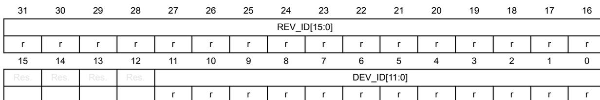
| 31 | 30 | 29 | 28 | 27 | 26 | 25 | 24 | 23 | 22 | 21 | 20 | 19 | 18 | 17 | 16 |
| REV_ID[15:0] | |||||||||||||||
| r | r | r | r | r | r | r | r | r | r | r | r | r | r | r | r |
| 15 | 14 | 13 | 12 | 11 | 10 | 9 | 8 | 7 | 6 | 5 | 4 | 3 | 2 | 1 | 0 |
| Res. | Res. | Res. | Res. | DEV_ID[11:0] | |||||||||||
| r | r | r | r | r | r | r | r | r | r | r | r | ||||
Bits 31:16 REV_ID[15:0] : Device revision
This field indicates the revision of the device. Refer to the device errata sheets ES0569 (STM32C011xx), ES0568 (STM32C031xx), ES0624 (STM32C051xx), ES0618 (STM32C071xx), and ES0625 (STM32C09xxx).
Bits 15:12 Reserved, must be kept at reset value.
Upon read, these reserved bits return 0b0110.
Bits 11:0 DEV_ID[11:0] : Device identifier
This field indicates the device ID. Refer to Table 177 .
Table 177. DEV_ID bitfield values
| Device | DEV_ID |
|---|---|
| STM32C011xx | 0x443 |
| STM32C031xx | 0x453 |
| STM32C051xx | 0x44C |
Table 177. DEV_ID bitfield values
| Device | DEV_ID |
|---|---|
| STM32C071xx | 0x493 |
| STM32C091xx/92xx | 0x44D |
30.10.2 DBG configuration register (DBG_CR)
Address offset: 0x0000 0004
Reset value: 0x0000 0000 (power-on reset)
Only 32-bit access supported.
This register configures the low-power modes of the MCU under debug.
It is asynchronously reset by the POR, but not affected by the system reset. It can be written by the debugger under system reset.
If the debugger host does not support this feature, it is still possible for the user software to write this register.
| 31 | 30 | 29 | 28 | 27 | 26 | 25 | 24 | 23 | 22 | 21 | 20 | 19 | 18 | 17 | 16 |
|---|---|---|---|---|---|---|---|---|---|---|---|---|---|---|---|
| Res. | Res. | Res. | Res. | Res. | Res. | Res. | Res. | Res. | Res. | Res. | Res. | Res. | Res. | Res. | Res. |
| 15 | 14 | 13 | 12 | 11 | 10 | 9 | 8 | 7 | 6 | 5 | 4 | 3 | 2 | 1 | 0 |
| Res. | Res. | Res. | Res. | Res. | Res. | Res. | Res. | Res. | Res. | Res. | Res. | Res. | DBG_STANDBY | DBG_STOP | Res. |
| rw | rw |
Bits 31:3 Reserved, must be kept at reset value.
Bit 2 DBG_STANDBY : Debug Standby and Shutdown modes
Debug options in Standby or Shutdown mode.
0: Digital part powered. From software point of view, exiting Standby and Shutdown modes is identical as fetching reset vector (except for status bits indicating that the MCU exits Standby)
1: Digital part powered and FCLK and HCLK running, derived from the internal RC oscillator remaining active. The MCU generates a system reset so that exiting Standby and Shutdown has the same effect as starting from reset.
Bit 1 DBG_STOP : Debug Stop mode
Debug options in Stop mode.
0: All clocks disabled, including FCLK and HCLK. Upon Stop mode exit, the CPU is clocked by the HSI internal RC oscillator.
1: FCLK and HCLK running, derived from the internal RC oscillator remaining active. If Systick is enabled, it may generate periodic interrupt and wake up events.
Upon Stop mode exit, the software must re-establish the desired clock configuration.
Bit 0 Reserved, must be kept at reset value.
30.10.3 DBG APB freeze register 1 (DBG_APB_FZ1)
Address offset: 0x08
Reset value: 0x0000 0000 (power-on reset)
Only 32-bit access are supported.
This register configures the clocking of timers, RTC, IWDG, WWDG, and I2C SMBUS peripherals of the MCU under debug:
The register is asynchronously reset by the POR but not affected by the system reset). It can be written by the debugger under system reset.
| 31 | 30 | 29 | 28 | 27 | 26 | 25 | 24 | 23 | 22 | 21 | 20 | 19 | 18 | 17 | 16 |
|---|---|---|---|---|---|---|---|---|---|---|---|---|---|---|---|
| Res. | Res. | Res. | Res. | Res. | Res. | Res. | Res. | Res. | Res. | DBG_I2C1_SMBUS_TIMEOUT | Res. | Res. | Res. | Res. | Res. |
| rw | |||||||||||||||
| 15 | 14 | 13 | 12 | 11 | 10 | 9 | 8 | 7 | 6 | 5 | 4 | 3 | 2 | 1 | 0 |
| Res. | Res. | Res. | DBG_IWDG_STOP | DBG_WWDG_STOP | DBG_RTC_STOP | Res. | Res. | Res. | Res. | Res. | Res. | Res. | Res. | DBG_TIM3_STOP | DBG_TIM2_STOP |
| rw | rw | rw | rw | rw |
Bits 31:22 Reserved, must be kept at reset value.
Bit 21 DBG_I2C1_SMBUS_TIMEOUT : SMBUS timeout when core is halted
0: Same behavior as in normal mode
1: The SMBUS timeout is frozen
Bits 20:13 Reserved, must be kept at reset value.
Bit 12 DBG_IWDG_STOP : Clocking of IWDG counter when the core is halted
This bit enables/disables the clock to the counter of IWDG when the core is halted:
0: Enable
1: Disable
Bit 11 DBG_WWDG_STOP : Clocking of WWDG counter when the core is halted
This bit enables/disables the clock to the counter of WWDG when the core is halted:
0: Enable
1: Disable
Bit 10 DBG_RTC_STOP : Clocking of RTC counter when the core is halted
This bit enables/disables the clock to the counter of RTC when the core is halted:
0: Enable
1: Disable
Bits 9:2 Reserved, must be kept at reset value.
Bit 1 DBG_TIM3_STOP : Clocking of TIM3 counter when the core is halted
This bit enables/disables the clock to the counter of TIM3 when the core is halted:
0: Enable
1: Disable
Bit 0 DBG_TIM2_STOP : Clocking of TIM2 counter when the core is halted
This bit enables/disables the clock to the counter of TIM2 when the core is halted:
0: Enable
1: Disable
This bit is only available on STM32C051xx, STM32C071xx, and STM32C091xx/92xx. On the other devices, it is reserved.
30.10.4 DBG APB freeze register 2 (DBG_APB_FZ2)
Address offset: 0x0C
Reset value: 0x0000 0000 (power-on reset)
Only 32-bit access is supported.
This register configures the clocking of timer counters when the MCU is under debug. It is asynchronously reset by the POR but not affected by the system reset. It can be written by the debugger under system reset.
| 31 | 30 | 29 | 28 | 27 | 26 | 25 | 24 | 23 | 22 | 21 | 20 | 19 | 18 | 17 | 16 |
|---|---|---|---|---|---|---|---|---|---|---|---|---|---|---|---|
| Res. | Res. | Res. | Res. | Res. | Res. | Res. | Res. | Res. | Res. | Res. | Res. | Res. | DBG_TIM17_STOP | DBG_TIM16_STOP | DBG_TIM15_STOP |
| RW | RW | RW | |||||||||||||
| 15 | 14 | 13 | 12 | 11 | 10 | 9 | 8 | 7 | 6 | 5 | 4 | 3 | 2 | 1 | 0 |
| DBG_TIM14_STOP | Res. | Res. | Res. | DBG_TIM1_STOP | Res. | Res. | Res. | Res. | Res. | Res. | Res. | Res. | Res. | Res. | Res. |
| RW | RW |
Bits 31:19 Reserved, must be kept at reset value.
Bit 18 DBG_TIM17_STOP : Clocking of TIM17 counter when the core is halted
This bit enables/disables the clock to the counter of TIM17 when the core is halted:
0: Enable
1: Disable
Bit 17 DBG_TIM16_STOP : Clocking of TIM16 counter when the core is halted
This bit enables/disables the clock to the counter of TIM16 when the core is halted:
0: Enable
1: Disable
Bit 16 DBG_TIM15_STOP : Clocking of TIM15 counter when the core is halted
This bit enables/disables the clock to the counter of TIM15 when the core is halted:
0: Enable
1: Disable
This bit is only available on STM32C091xx/92xx. On the other devices, it is reserved.
Bit 15 DBG_TIM14_STOP : Clocking of TIM14 counter when the core is halted
This bit enables/disables the clock to the counter of TIM14 when the core is halted:
0: Enable
1: Disable
Bits 14:12 Reserved, must be kept at reset value.
Bit 11 DBG_TIM1_STOP : Clocking of TIM1 counter when the core is halted
This bit enables/disables the clock to the counter of TIM1 when the core is halted:
0: Enable
1: Disable
Bits 10:0 Reserved, must be kept at reset value.
30.10.5 DBG register map
The following table summarizes the DBG registers.
Table 178. DBG register map and reset values
| Offset | Register | 31 | 30 | 29 | 28 | 27 | 26 | 25 | 24 | 23 | 22 | 21 | 20 | 19 | 18 | 17 | 16 | 15 | 14 | 13 | 12 | 11 | 10 | 9 | 8 | 7 | 6 | 5 | 4 | 3 | 2 | 1 | 0 | |
|---|---|---|---|---|---|---|---|---|---|---|---|---|---|---|---|---|---|---|---|---|---|---|---|---|---|---|---|---|---|---|---|---|---|---|
| 0x00 | DBG_IDCODE | REV_ID | Res. | Res. | Res. | Res. | DEV_ID | |||||||||||||||||||||||||||
| Reset value (1) | U | U | U | U | U | U | U | U | U | U | U | U | U | U | U | U | 0 | 1 | 1 | 0 | U | U | U | U | U | U | U | U | U | U | U | U | U | |
| 0x04 | DBG_CR | Res. | Res. | Res. | Res. | Res. | Res. | Res. | Res. | Res. | Res. | Res. | Res. | Res. | Res. | Res. | Res. | Res. | Res. | Res. | Res. | Res. | Res. | Res. | Res. | Res. | Res. | Res. | Res. | Res. | Res. | DBG_STANDBY | DBG_STOP | Res. |
| Reset value | 0 | 0 | ||||||||||||||||||||||||||||||||
| 0x08 | DBG_APB_FZ1 | Res. | Res. | Res. | Res. | Res. | Res. | Res. | Res. | Res. | Res. | Res. | Res. | Res. | Res. | Res. | Res. | Res. | Res. | Res. | DBG_IWDG_STOP | DBG_WWDG_STOP | DBG_RTC_STOP | Res. | Res. | Res. | Res. | Res. | Res. | Res. | Res. | Res. | DBG_TIM3_STOP | DBG_TIM2_STOP |
| Reset value | 0 | 0 | 0 | 0 | 0 | |||||||||||||||||||||||||||||
| 0x0C | DBG_APB_FZ2 | Res. | Res. | Res. | Res. | Res. | Res. | Res. | Res. | Res. | Res. | Res. | Res. | Res. | Res. | Res. | Res. | Res. | Res. | Res. | Res. | DBG_TIM1_STOP | Res. | Res. | Res. | Res. | Res. | Res. | Res. | Res. | Res. | Res. | Res. | |
| Reset value | 0 | |||||||||||||||||||||||||||||||||
1. The reset value is product dependent. For more information, refer to Section 30.10.1: DBG device ID code register (DBG_IDCODE) .
Refer to Section 2.2 on page 45 for the register boundary addresses.