29. Universal serial bus full-speed host/device interface (USB)
This section applies to STM32C071 devices only.
29.1 Introduction
The USB peripheral implements an interface between a full-speed USB 2.0 bus and the APB bus.
USB suspend/resume are supported, which permits to stop the device clocks for low-power consumption.
29.2 USB main features
- • USB specification version 2.0 full-speed compliant
- • Supports both Host and Device modes
- • Configurable number of endpoints from 1 to 8
- • Dedicated packet buffer memory (SRAM) of 2048 bytes
- • Cyclic redundancy check (CRC) generation/checking, Non-return-to-zero Inverted (NRZI) encoding/decoding and bit-stuffing
- • Isochronous transfers support
- • Double-buffered bulk/isochronous endpoint/channel support
- • USB Suspend/Resume operations
- • Frame locked clock pulse generation
- • USB 2.0 Link Power Management support (Device mode only)
- • Battery Charging Specification Revision 1.2 support (Device mode only)
- • USB connect / disconnect capability (controllable embedded pull-up resistor on USB_DP line)
29.3 USB implementation
Table 154 describes the USB implementation in the devices.
Table 154. STM32C0 series USB implementation
| USB features (1) | USB |
|---|---|
| Host mode | X |
| Number of endpoints | 8 |
| Size of dedicated packet buffer memory SRAM | 2048 bytes |
| Dedicated packet buffer memory SRAM access scheme | 32 bits |
| USB 2.0 Link Power Management (LPM) support in device | X |
Table 154. STM32C0 series USB implementation (continued)
| USB features (1) | USB |
|---|---|
| Battery Charging Detection (BCD) support for device | X |
| Embedded pull-up resistor on USB_DP line | X |
1. X= supported
29.4 USB functional description
29.4.1 USB block diagram
Figure 326 shows the block diagram of the USB peripheral.
Figure 326. USB peripheral block diagram
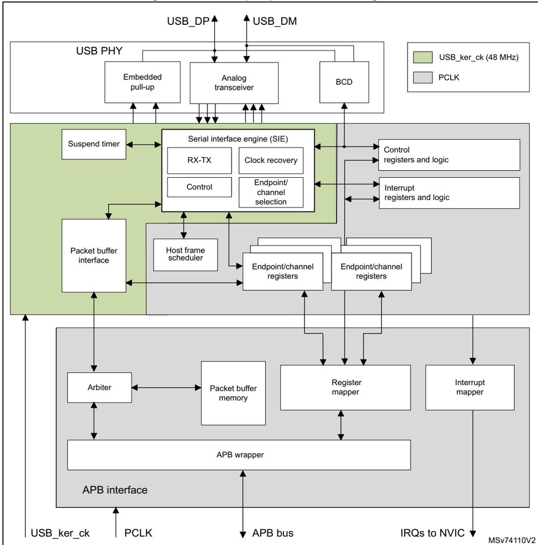
The block diagram illustrates the internal architecture of the USB peripheral. At the top, the USB PHY block contains an Embedded pull-up , an Analog transceiver , and a BCD (Battery Charging Detection) block. The Analog transceiver is connected to external USB_DP and USB_DM pins. Below the PHY, the Serial interface engine (SIE) is shown, which includes RX-TX , Clock recovery , Control , and Endpoint/channel selection sub-blocks. The SIE is connected to a Suspend timer , Packet buffer interface , Host frame scheduler , Control registers and logic , and Interrupt registers and logic . The Host frame scheduler and Packet buffer interface are connected to multiple Endpoint/channel registers . These registers are then connected to an Arbiter , Packet buffer memory , Register mapper , and Interrupt mapper . The Arbiter and Packet buffer memory are connected to an APB wrapper , which is part of the APB interface . The APB interface is connected to the APB bus . External clock inputs USB_ker_ck (48 MHz) and PCLK are shown at the bottom left. The Interrupt mapper outputs IRQs to NVIC at the bottom right. A legend indicates that green blocks represent USB_ker_ck (48 MHz) and grey blocks represent PCLK . The diagram is labeled MSV74110V2.
29.4.2 USB pins and internal signals
Table 155. USB input/output pins
| Pin name | Pin type | Description |
|---|---|---|
| USB_DP | Digital input/output | D+ line |
| USB_DM | Digital input/output | D- line |
29.4.3 USB reset and clocks
A single reset is present on USB. The RCC allows a reset to be forced by software.
There are two clocks:
- • PCLK for the APB bus interface and registers.
- • USB_ker_ck (48 MHz) for the main protocol logic including notably the serial interface engine (SIE), see USB_ker_ck clock domain in block diagram.
29.4.4 General description and Device mode functionality
The USB peripheral provides a USB-compliant connection between the function implemented by the microcontroller and an external USB function which can be a host PC but also a USB Device. Data transfer between the external USB host or device and the system memory occurs through a dedicated packet buffer memory accessed directly by the USB peripheral. This dedicated memory size is 2048 bytes, and up to 16 mono-directional or 8 bidirectional endpoints can be used. The USB peripheral interfaces with the external USB Host or Device, detecting token packets, handling data transmission/reception, and processing handshake packets as required by the USB standard. Transaction formatting is performed by the hardware, including CRC generation and checking.
Each endpoint/channel is associated with a buffer description block indicating where the endpoint/channel-related memory area is located, how large it is or how many bytes must be transmitted. When a token for a valid function/endpoint pair is recognized by the USB peripheral, the related data transfer (if required and if the endpoint/channel is configured) takes place. The data buffered by the USB peripheral are loaded in an internal 16-bit register and memory access to the dedicated buffer is performed. When all the data have been transferred, if needed, the proper handshake packet over the USB is generated or expected according to the direction of the transfer.
At the end of the transaction, an endpoint/channel-specific interrupt is generated, reading status registers and/or using different interrupt response routines. The microcontroller can determine:
- • which endpoint/channel has to be served,
- • which type of transaction took place, if errors occurred (bit stuffing, format, CRC, protocol, missing ACK, over/underrun, etc.).
Special support is offered to isochronous transfers and high throughput bulk transfers, implementing a double buffer usage, which permits to always have an available buffer for the USB peripheral while the microcontroller uses the other one.
A special bit THR512 in register USB_ISTR allows notification of 512 bytes being received in (or transmitted from) the buffer. This bit must be used for long ISO packets (from 512 to 1023 bytes) as it facilitates early start or read/write of data. In this way, the first 512 bytes
can be handled by software while avoiding use of double buffer mode. This bit works when only one ISO endpoint is configured.
The unit can be placed in low-power mode (SUSPEND mode), by writing in the control register, whenever required. At this time, all static power dissipation is avoided, and the USB clock can be slowed down or stopped. The detection of activity at the USB inputs, while in low-power mode, wakes the device up asynchronously. A special interrupt source can be connected directly to a wake-up line to permit the system to immediately restart the normal clock generation and/or support direct clock start/stop.
Host mode and specific functionality
A single bit, HOST, in register USB_CNTR permits Host mode to be activated. Host mode functionality permits the USB to talk to a remote peripheral. Supported functionality is aligned to Device mode and uses the same register structures to manage the buffers. The same number of endpoints can be supported in Host mode, however in Host mode the terminology “channel” is preferred, as each channel is in reality a combination of the connected device and the endpoint on that device. The basic mechanisms for packet transmission and reception are the same as those supported in Device mode.
When operating in Host mode, the USB is in charge of the bus and in order to do this must issue transaction requests corresponding to active periodic and non-periodic endpoints. A host frame scheduler assures efficient use of the frame. Connection to hubs is supported. Connection to low speed devices is supported, both with a direct connection and through a hub.
Double-buffered mode, as previously described in Device mode, is also supported in Host mode, in both bulk and isochronous channels. The THR512 functionality is also supported (but as in Device mode) only for ISO traffic.
Note: Unlike in Device mode, where there is a detection of battery charging capability (in order to facilitate fast charging), there is no integrated support in Host mode to present battery charging capability (CDP or DCP cases in the standard), the host port is always presented as a default standard data port (SDP).
For LPM (link power management) this feature is not supported in Host mode.
29.4.5 Description of USB blocks used in both Device and Host modes
The USB peripheral implements all the features related to USB interfacing, which include the following blocks:
- • USB physical interface (USB PHY): this block is maintaining the electrical interface to an external USB host. It contains the differential analog transceiver itself, controllable embedded pull-up resistor (connected to USB_DP line) and support for battery charging detection (BCD), multiplexed on same USB_DP and USB_DM lines.
- • Serial interface engine (SIE): the functions of this block include: synchronization pattern recognition, bit-stuffing, CRC generation and checking, PID verification/generation, and handshake evaluation. It must interface with the USB transceivers and uses the virtual buffers provided by the packet buffer interface for local data storage. This unit also generates signals according to USB peripheral events, such as start of frame (SOF), USB_Reset, data errors etc. and to endpoint
related events like end of transmission or correct reception of a packet; these signals are then used to generate interrupts.
- • Timer: this block generates a start-of-frame locked clock pulse and detects a global suspend (from the host) when no traffic has been received for 3 ms.
- • Packet buffer interface: this block manages the local memory implementing a set of buffers in a flexible way, both for transmission and reception. It can choose the proper buffer according to requests coming from the SIE and locate them in the memory addresses pointed by the endpoint/channel registers. It increments the address after each exchanged byte until the end of packet, keeping track of the number of exchanged bytes and preventing the buffer to overrun the maximum capacity.
- • Endpoint/channel-related registers: each endpoint/channel has an associated register containing the endpoint/channel type and its current status. For mono-directional/single-buffer endpoints, a single register can be used to implement two distinct endpoints. The number of registers is 8, allowing up to 16 mono-directional/single-buffer or up to 7 double-buffer endpoints in any combination. For example the USB peripheral can be programmed to have 4 double buffer endpoints and 8 single-buffer/mono-directional endpoints.
- • Control registers: these are the registers containing information about the status of the whole USB peripheral and used to force some USB events, such as resume and power-down.
- • Interrupt registers: these contain the interrupt masks and a record of the events. They can be used to inquire an interrupt reason, the interrupt status or to clear the status of a pending interrupt.
Note: * Endpoint/channel 0 is always used for control transfer in single-buffer mode.
The USB peripheral is connected to the APB bus through an APB interface, containing the following blocks:
- • Packet memory: this is the local memory that physically contains the packet buffers. It can be used by the packet buffer interface, which creates the data structure and can be accessed directly by the application software. The size of the packet memory is 2048 bytes, structured as 512 words of 32 bits.
- • Arbiter: this block accepts memory requests coming from the APB bus and from the USB interface. It resolves the conflicts by giving priority to APB accesses, while always reserving half of the memory bandwidth to complete all USB transfers. This time-duplex scheme implements a virtual dual-port SRAM that allows memory access, while an USB transaction is happening. Multiword APB transfers of any length are also allowed by this scheme.
- • Register mapper: this block collects the various byte-wide and bit-wide registers of the USB peripheral in a structured 32-bit wide word set addressed by the APB.
- • APB wrapper: this provides an interface to the APB for the memory and register. It also maps the whole USB peripheral in the APB address space.
- • Interrupt mapper: this block is used to select how the possible USB events can generate interrupts and map them to the NVIC.
29.4.6 Description of host frame scheduler (HFS) specific to Host mode
The host frame scheduler is the hardware machine in charge to submit host channel requests on the bus according to the USB priority order and bandwidth access rules.
Host channels are divided in two categories:
- – Periodic channels: isochronous and interrupt traffic types. With guaranteed bandwidth access.
- – Non-periodic channels: bulk and control traffic types. With best effort service.
The host frame scheduler organizes the full-speed frame in 3 sequential windows
- – Periodic service window
- – Non-periodic service window
- – Black security window
At the start of a new frame, the host scheduler:
- 1. First considers all periodic channels which were active (STAT bits VALID) at the start of frame
- 2. Executes single round of service of periodic channels, the periodic service window, in hardware priority order from CH#1 to CH#8. For bidirectional channels it executes the OUT direction first
- 3. When the periodic round is finished, HFS closes the periodic service window and stops servicing periodic traffic even if some periodic channel was re-enabled or some new channel was enabled after the SOF.
- 4. Starts servicing all non-periodic channels which are currently active (STAT bits VALID) in hardware priority order from CH#1 to CH#8. For bidirectional channels it executes the OUT direction first.
- 5. Executes multiple round-robin service cycles of non-periodic channels until almost the end of frame
- 6. Non-periodic traffic can be requested at any time and is serviced by HFS with best effort latency, with the exception of a black security window at the end of the frame where new injected requests are directly postponed to the next frame to avoid babbles. This is also true for pending transactions which have not been serviced ahead of the security window.
29.5 Programming considerations for Device and Host modes
In the following sections, the expected interactions between the USB peripheral and the application program are described, in order to ease application software development.
29.5.1 Generic USB Device programming
This part describes the main tasks required of the application software in order to obtain USB compliant behavior. The actions related to the most general USB events are taken into account and paragraphs are dedicated to the special cases of double-buffered endpoints and isochronous transfers. Apart from system reset, an action is always initiated by the USB peripheral, driven by one of the USB events described below.
29.5.2 System and power-on reset
Upon system and power-on reset, the first operation the application software must perform is to provide all required clock signals to the USB peripheral and subsequently de-assert its reset signal so to be able to access its registers. The whole initialization sequence is hereafter described.
As a first step application software needs to activate register macrocell clock and de-assert macrocell specific reset signal using related control bits provided by device clock management logic.
After that, the analog part of the device related to the USB transceiver must be switched on using the PDWN bit in CNTR register, which requires a special handling. This bit is intended to switch on the internal voltage references that supply the port transceiver. This circuit has a defined startup time ( \( t_{STARTUP} \) specified in the datasheet) during which the behavior of the USB transceiver is not defined. It is thus necessary to wait this time, after setting the PDWN bit in the CNTR register, before removing the reset condition on the USB part (by clearing the USBRST bit in the CNTR register). Clearing the ISTR register removes any spurious pending interrupt before any other macrocell operation is enabled.
At system reset, the microcontroller must initialize all required registers and the packet buffer description table, to make the USB peripheral able to properly generate interrupts and data transfers. All registers not specific to any endpoint/channel must be initialized according to the needs of application software (choice of enabled interrupts, chosen address of packet buffers, etc.). Then the process continues as for the USB reset case (see further paragraph).
USB bus reset (RST_DCON interrupt) in Device mode
When this event occurs, the USB peripheral is put in the same conditions it is left by the system reset after the initialization described in the previous paragraph: communication is disabled in all endpoint registers (the USB peripheral does not respond to any packet). As a response to the USB reset event, the USB function must be enabled, having as USB address 0, implementing only the default control endpoint (endpoint address is 0 too). This is accomplished by setting the enable function (EF) bit of the USB_DADDR register and initializing the CHEP0R register and its related packet buffers accordingly. During USB enumeration process, the host assigns a unique address to this device, which must be written in the ADD[6:0] bits of the USB_DADDR register, and configures any other necessary endpoint.
When a RST_DCON interrupt is received, the application software is responsible to enable again the default endpoint of USB function 0 within 10 ms from the end of the reset sequence which triggered the interrupt.
USB bus reset in Host mode
In Host mode a bus reset is activated by setting the USBRST bit of the USB_CNTR register. It must subsequently be cleared by software once the minimum active reset time from the standard has been respected.
Structure and usage of packet buffers
Each bidirectional endpoint can receive or transmit data over the bus. The received data is stored in a dedicated memory buffer reserved for that endpoint, while another memory buffer contains the data to be transmitted by the endpoint. Access to this memory is performed by the packet buffer interface block, which delivers a memory access request
and waits for its acknowledgment. Since the packet buffer memory has also to be accessed by the microcontroller, an arbitration logic takes care of the access conflicts, using half APB cycle for microcontroller access and the remaining half for the USB peripheral access. In this way, both agents can operate as if the packet memory would be a dual-port SRAM, without being aware of any conflict even when the microcontroller is performing back-to-back accesses. The USB peripheral logic uses a dedicated clock. The frequency of this dedicated clock is fixed by the requirements of the USB standard at 48 MHz, and this can be different from the clock used for the interface to the APB bus. Different clock configurations are possible where the APB clock frequency can be higher or lower than the USB peripheral one.
Note: Due to USB data rate and packet memory interface requirements, the APB clock must have a minimum frequency of 12 MHz to avoid data overrun/underrun problems.
Each endpoint is associated with two packet buffers (usually one for transmission and the other one for reception). Buffers can be placed anywhere inside the packet memory because their location and size is specified in a buffer description table, which is also located in the packet memory. Each table entry is associated to an endpoint register and it is composed of two 32-bit words so that table start address must always be aligned to an 8-byte boundary. Buffer descriptor table entries are described in Section 29.7: USB SRAM registers . If an endpoint is unidirectional and it is neither an isochronous nor a double-buffered bulk, only one packet buffer is required (the one related to the supported transfer direction). Other table locations related to unsupported transfer directions or unused endpoints, are available to the user. Isochronous and double-buffered bulk endpoints have special handling of packet buffers (Refer to Section 29.5.5: Isochronous transfers in Device mode and Section 29.5.3: Double-buffered endpoints and usage in Device mode respectively). The relationship between buffer description table entries and packet buffer areas is depicted in Figure 327 .
For Host mode different sections explain the buffer usage model, notably Section 29.5.6: Isochronous transfers in Host mode and Section 29.5.4: Double buffered channels: usage in Host mode .
Figure 327. Packet buffer areas with examples of buffer description table locations
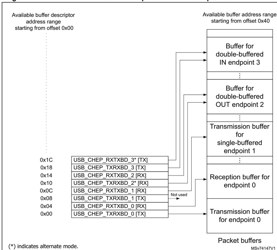
Available buffer descriptor address range starting from offset 0x00
| 0x1C | USB_CHEP_RXTXBD_3* [TX] | |
| 0x18 | USB_CHEP_TXRXBD_3 [TX] | |
| 0x14 | USB_CHEP_RXTXBD_2 [RX] | |
| 0x10 | USB_CHEP_TXRXBD_2* [RX] | |
| 0x0C | USB_CHEP_RXTXBD_1 [RX] | |
| 0x08 | USB_CHEP_TXRXBD_1 [TX] | Not used |
| 0x04 | USB_CHEP_RXTXBD_0 [RX] | |
| 0x00 | USB_CHEP_TXRXBD_0 [TX] |
Available buffer address range starting from offset 0x40
Packet buffers
- Buffer for double-buffered IN endpoint 3
- Buffer for double-buffered OUT endpoint 2
- Transmission buffer for single-buffered endpoint 1
- Reception buffer for endpoint 0
- Transmission buffer for endpoint 0
(*) indicates alternate mode.
MSV74147V1
Each packet buffer is used either during reception or transmission starting from the bottom. The USB peripheral never changes the contents of memory locations adjacent to the allocated memory buffers; if a packet bigger than the allocated buffer length is received (buffer overrun condition) the data is copied to the memory only up to the last available location.
Endpoint initialization
The first step to initialize an endpoint is to write appropriate values to the ADDRn_TX/ADDRn_RX fields in the CHEP_TXBD_n and CHEP_RXBD_n registers (in SRAM) so that the USB peripheral finds the data to be transmitted already available and the data to be received can be buffered. The UTYPE bits in the USB_CHEPnR register must be set according to the endpoint type, eventually using the EPKIND bit to enable any special required feature. On the transmit side, the endpoint must be enabled using the STATTX bits in the USB_CHEPnR register and COUNTn_TX must be initialized. For reception, STATRX bits must be set to enable reception and COUNTn_RX must be written with the allocated buffer size using the BLSIZE and NUM_BLOCK fields. Unidirectional endpoints, except isochronous and double-buffered bulk endpoints, need to initialize only bits and registers related to the supported direction. Once the transmission and/or reception are enabled, register USB_CHEPnR and locations ADDRn_TX/ADDRn_RX, COUNTn_TX/COUNTn_RX (respectively), must not be modified by the application software, as the hardware can
change their value on the fly. When the data transfer operation is completed, notified by a CTR interrupt event, they can be accessed again to re-enable a new operation.
Data transmission in Device mode (IN packets)
When receiving an IN token packet, if the received address matches a configured and valid endpoint, the USB peripheral accesses the contents of CHEP_TXBD_n (fields ADDRn_TX and COUNTn_TX) inside the buffer descriptor table entry related to the addressed endpoint. The content of these locations is stored in its internal 16-bit registers ADDR and COUNT (not accessible by software). The packet memory is accessed again to read the first byte to be transmitted (refer to Structure and usage of packet buffers on page 959 ) and the USB peripheral starts sending a DATA0 or DATA1 PID according to USB_CHEPnR bit DTOGTX. When the PID is completed, the first byte, read from buffer memory, is loaded into the output shift register to be transmitted on the USB bus. After the last data byte is transmitted, the computed CRC is sent. If the addressed endpoint is not valid, a NAK or STALL handshake packet is sent instead of the data packet, according to STATTX bits in the USB_CHEPnR register.
The ADDRn_TX field in the internal register CHEP_TXBD_n is used as a pointer to the current buffer memory location while COUNT is used to count the number of remaining bytes to be transmitted. Each half-word read from the packet buffer memory is transmitted over the USB bus starting from the least significant byte. Transmission buffer memory is read starting from the address pointed by ADDRn_TX for COUNTn_TX/4 words. If a transmitted packet is composed of an odd number of bytes, only the lower half of the last half-word accessed is used.
On receiving the ACK receipt by the host, the USB_CHEPnR register is updated in the following way: DTOGTX bit is toggled, the endpoint is made invalid by setting STATTX = 10 (NAK) and bit VTTX is set. The application software must first identify the endpoint, which is requesting microcontroller attention by examining the IDN and DIR bits in the USB_ISTR register. Servicing of the VTTX event starts, clearing the interrupt bit; the application software then prepares another buffer full of data to be sent, updates the COUNTn_TX table location with the number of byte to be transmitted during the next transfer, and finally sets STATTX to 11 (VALID) to re-enable transmission. While the STATTX bits are equal to 10 (NAK), any IN request addressed to that endpoint is NAKed, indicating a flow control condition: the USB host retries the transaction until it succeeds. It is mandatory to execute the sequence of operations in the above mentioned order to avoid losing the notification of a second IN transaction addressed to the same endpoint immediately following the one which triggered the CTR interrupt.
Data transmission in Host mode (OUT packets)
Data transmission in Host mode follows the same general principles as Device mode. The main differences are due to the protocol. For example the host initiates the transmission whereas the device responds to the incoming token.
ADDRn_TX must be set to the location in the packet memory reserved for the packet for transmission. The contents of an OUT packet are then written to that address in the packet memory and COUNTn_TX must be updated (when necessary) to indicate the number of bytes in the packet.
DEVADDR must be written for the correct endpoint and then STATTX must be set to 11 (VALID) in order to trigger the transmit. The transmission is then scheduled by the HFS.
After a successful transmission the CTR interrupt (correct transfer) is triggered. By examining IDN and DIR bits, the corresponding channel and direction is understood. On the
indicated channel, the STATTX field now has transitioned to DISABLE. In the case of a NAK being received (when the peripheral is not ready) STATTX is now in NAK. In the case of a STALL response, STATTX is in STALL. In this last case, the bus must be reset.
On receiving the ACK receipt by the device, the USB_CHEPnR register is updated in the following way: DTOGTX bit is toggled.
An error condition is signaled via the bits VTTX and ERR_TX if one of the following conditions occurs:
- • No handshake being received in time
- • False EOP
- • Bit stuffing error
- • Invalid handshake PID
Data reception in Device mode (OUT and SETUP packets)
These two tokens are handled by the USB peripheral more or less in the same way; the differences in the handling of SETUP packets are detailed in the following paragraph about control transfers. When receiving an OUT/SETUP PID, if the address matches a valid endpoint, the USB peripheral accesses the contents of the ADDRn_RX and COUNTn_RX fields inside the buffer descriptor table entry related to the addressed endpoint. The content of the ADDRn_RX field is stored directly in its internal register ADDR. Internal register COUNT is now reset and the values of BLSIZE and NUM_BLOCK bit fields, which are read within USB_CHEP_RXBD_n content, are used to initialize BUF_COUNT, an internal 16-bit counter, which is used to check the buffer overrun condition (all these internal registers are not accessible by software). Data bytes subsequently received by the USB peripheral are packed in half-words (the first byte received is stored as least significant byte) and then transferred to the packet buffer starting from the address contained in the internal ADDR register while BUF_COUNT is decremented and COUNT is incremented at each byte transfer. When the end of DATA packet is detected, the correctness of the received CRC is tested and only if no errors occurred during the reception, an ACK handshake packet is sent back to the transmitting host.
In case of wrong CRC or other kinds of errors (bit-stuff violations, frame errors, etc.), data bytes are still copied in the packet memory buffer, at least until the error detection point, but the ACK packet is not sent and the ERR bit in USB_ISTR register is set. However, there is usually no software action required in this case: the USB peripheral recovers from reception errors and remains ready for the next transaction to come. If the addressed endpoint is not valid, a NAK or STALL handshake packet is sent instead of the ACK, according to bits STATRX in the USB_CHEPnR register, and no data is written in the reception memory buffers.
Reception memory buffer locations are written starting from the address contained in the ADDRn_RX for a number of bytes corresponding to the received data packet length, or up to the last allocated memory location, as defined by BLSIZE and NUM_BLOCK, whichever comes first. In this way, the USB peripheral never writes beyond the end of the allocated reception memory buffer area. If the length of the data packet payload (actual number of bytes used by the application) is greater than the allocated buffer, the USB peripheral detects a buffer overrun condition. In this case, a STALL handshake is sent instead of the usual ACK to notify the problem to the host, no interrupt is generated and the transaction is considered failed.
When the transaction is completed correctly, by sending the ACK handshake packet, the internal COUNT register is copied back in the COUNTn_RX location inside the buffer
description table entry, leaving unaffected BLSIZE and NUM_BLOCK fields, which normally do not require to be re-written, and the USB_CHEPnR register is updated in the following way: DTOGRX bit is toggled, the endpoint is made invalid by setting STATRX = 10 (NAK) and bit VTRX is set. If the transaction has failed due to errors or buffer overrun condition, none of the previously listed actions take place. The application software must first identify the endpoint, which is requesting microcontroller attention by examining the IDN and DIR bits in the USB_ISTR register. The VTRX event is serviced by first determining the transaction type (SETUP bit in the USB_CHEPnR register); the application software must clear the interrupt flag bit and get the number of received bytes reading the COUNTn_RX location inside the buffer description table entry related to the endpoint being processed. After the received data is processed, the application software must set the STATRX bits to 11 (VALID) in the USB_CHEPnR, enabling further transactions. While the STATRX bits are equal to 10 (NAK), any OUT request addressed to that endpoint is NAKed, indicating a flow control condition: the USB host retries the transaction until it succeeds. It is mandatory to execute the sequence of operations in the above mentioned order to avoid losing the notification of a second OUT transaction addressed to the same endpoint following immediately the one which triggered the CTR interrupt.
Data reception in Host mode (IN packets)
Data reception in Host mode follows the same general principles as Device mode. The main differences are again due to the protocol. In the device, data can be received or not, depending on readiness after previous operations, whereas the host only requests receive data when it is ready and able to store them.
ADDRn_TX must be set to the location in the packet memory reserved for the packet for transmission. The contents received in the data phase response to the IN token packet are then written to that address in the packet memory and COUNTn_TX gets updated by hardware during this process to indicate the number of bytes in the packet.
DEVADDR must be written for the correct endpoint and then STATRX must be set to VALID in order to trigger the reception. The reception is then scheduled by the HFS.
After a successful reception the interrupt CTR (correct transfer) is triggered. By examining IDN and DIR bits, the corresponding channel and direction is understood. On the indicated channel, the STATRX field now has transitioned to DISABLE. In the case of a NAK being received (when the peripheral is not ready) STATRX now is in NAK. In the case of a STALL response, STATRX is in STALL. In this last case, the bus must be reset. During an IN packet an error condition is signaled via the bits VTRX and ERR_RX if one of the following conditions occurs:
- • False EOP
- • Bit stuffing error
- • Wrong CRC
Control transfers in Device mode
Control transfers are made of a SETUP transaction, followed by zero or more data stages, all of the same direction, followed by a status stage (a zero-byte transfer in the opposite direction). SETUP transactions are handled by control endpoints only and are very similar to OUT ones (data reception) except that the values of DTOGTX and DTOGRX bits of the addressed endpoint registers are set to 1 and 0 respectively, to initialize the control transfer, and both STATTX and STATRX are set to 10 (NAK) to let software decide if subsequent transactions must be IN or OUT depending on the SETUP contents. A control endpoint must check SETUP bit in the USB_CHEPnR register at each VTRX event to distinguish normal
OUT transactions from SETUP ones. A USB Device can determine the number and direction of data stages by interpreting the data transferred in the SETUP stage, and is required to STALL the transaction in the case of errors. To do so, at all data stages before the last, the unused direction must be set to STALL, so that, if the host reverses the transfer direction too soon, it gets a STALL as a status stage.
While enabling the last data stage, the opposite direction must be set to NAK, so that, if the host reverses the transfer direction (to perform the status stage) immediately, it is kept waiting for the completion of the control operation. If the control operation completes successfully, the software changes NAK to VALID, otherwise to STALL. At the same time, if the status stage is an OUT, the STATUS_OUT (EPKIND in the USB_CHEPnR register) bit must be set, so that an error is generated if a status transaction is performed with non-zero data. When the status transaction is serviced, the application clears the STATUS_OUT bit and sets STATRX to VALID (to accept a new command) and STATTX to NAK (to delay a possible status stage immediately following the next setup).
Since the USB specification states that a SETUP packet cannot be answered with a handshake different from ACK, eventually aborting a previously issued command to start the new one, the USB logic does not permit a control endpoint to answer with a NAK or STALL packet to a SETUP token received from the host.
When the STATRX bits are set to 01 (STALL) or 10 (NAK) and a SETUP token is received, the USB accepts the data, performing the required data transfers and sends back an ACK handshake. If that endpoint has a previously issued VTRX request not yet acknowledged by the application (for example VTRX bit is still set from a previously completed reception), the USB discards the SETUP transaction and does not answer with any handshake packet regardless of its state, simulating a reception error and forcing the host to send the SETUP token again. This is done to avoid losing the notification of a SETUP transaction addressed to the same endpoint immediately following the transaction, which triggered the VTRX interrupt.
Control transfers in Host mode
Control transfers are made of a SETUP transaction, followed by zero or more data stages, all of the same direction, followed by a status stage (a zero-byte transfer in the opposite direction). SETUP transactions are handled by control endpoints only. A control endpoint must set the SETUP bit in the USB_CHEPnR register. The values of DTOGTX and DTOGRX bits of the addressed endpoint registers are set to 0. Depending on whether it is a control write or control read then STATTX or STATRX are set to 11 (ACTIVE) in order to trigger the control transfer via the host frame scheduler.
On receiving a CTR interrupt the channel (device address and endpoint) can be determined by examining IDN and DIR bits. Devices are expected to NAK every control unless the packet is corrupted in which case they do not acknowledge. The situation is reflected in the value of STATTX.
In the case of an error condition the ERR bit gets set. One possible case is where a CRC error is seen at the device, in this case no ACK is returned to the host. The host sees no ACK and after an appropriate delay this generates a timeout error with ERR_TX set (which can generate an interrupt).
29.5.3 Double-buffered endpoints and usage in Device mode
All different endpoint types defined by the USB standard represent different traffic models, and describe the typical requirements of different kind of data transfer operations. When large portions of data are to be transferred between the host PC and the USB function, the bulk endpoint type is the most suited model. This is because the host schedules bulk transactions so as to fill all the available bandwidth in the frame, maximizing the actual transfer rate as long as the USB function is ready to handle a bulk transaction addressed to it. If the USB function is still busy with the previous transaction when the next one arrives, it answers with a NAK handshake and the host PC issues the same transaction again until the USB function is ready to handle it, reducing the actual transfer rate due to the bandwidth occupied by re-transmissions. For this reason, a dedicated feature called 'double-buffering' can be used with bulk endpoints.
When 'double-buffering' is activated, data toggle sequencing is used to select, which buffer is to be used by the USB peripheral to perform the required data transfers, using both 'transmission' and 'reception' packet memory areas to manage buffer swapping on each successful transaction in order to always have a complete buffer to be used by the application, while the USB peripheral fills the other one. For example, during an OUT transaction directed to a 'reception' double-buffered bulk endpoint, while one buffer is being filled with new data coming from the USB host, the other one is available for the microcontroller software usage (the same would happen with a 'transmission' double-buffered bulk endpoint and an IN transaction).
Since the swapped buffer management requires the usage of all 4 buffer description table locations hosting the address pointer and the length of the allocated memory buffers, the USB_CHEPnR registers used to implement double-buffered bulk endpoints are forced to be used as unidirectional ones. Therefore, only one STAT bit pair must be set at a value different from 00 (DISABLED): STATRX if the double-buffered bulk endpoint is enabled for reception, STATTX if the double-buffered bulk endpoint is enabled for transmission. In case it is required to have double-buffered bulk endpoints enabled both for reception and transmission, two USB_CHEPnR registers must be used.
To exploit the double-buffering feature and reach the highest possible transfer rate, the endpoint flow control structure, described in previous chapters, has to be modified, in order to switch the endpoint status to NAK only when a buffer conflict occurs between the USB peripheral and application software, instead of doing it at the end of each successful transaction. The memory buffer which is currently being used by the USB peripheral is defined by the DTOG bit related to the endpoint direction: DTOGRX (bit 14 of USB_CHEPnR register) for 'reception' double-buffered bulk endpoints or DTOGTX (bit 6 of USB_CHEPnR register) for 'transmission' double-buffered bulk endpoints. To implement the new flow control scheme, the USB peripheral must know which packet buffer is currently in use by the application software, so to be aware of any conflict. Since in the USB_CHEPnR register, there are two DTOG bits but only one is used by USB peripheral for data and buffer sequencing (due to the unidirectional constraint required by double-buffering feature) the other one can be used by the application software to show which buffer it is currently using. This new buffer flag is called SW_BUF. In the following table the correspondence between USB_CHEPnR register bits and DTOG/SW_BUF definition is explained, for the cases of 'transmission' and 'reception' double-buffered bulk endpoints.
Table 156. Double-buffering buffer flag definition| Buffer flag | 'Transmission' endpoint | 'Reception' endpoint |
|---|---|---|
| DTOG | DTOGTX (USB_CHEPnR bit 6) | DTOGRX (USB_CHEPnR bit 14) |
| SW_BUF | USB_CHEPnR bit 14 | USB_CHEPnR bit 6 |
The memory buffer which is currently being used by the USB peripheral is defined by DTOG buffer flag, while the buffer currently in use by application software is identified by SW_BUF buffer flag. The relationship between the buffer flag value and the used packet buffer is the same in both cases, and it is listed in the following table.
Table 157. Bulk double-buffering memory buffers usage (Device mode)| Endpoint type | DTOG | SW_BUF | Packet buffer used by USB peripheral | Packet buffer used by Application Software |
|---|---|---|---|---|
| Transmit (IN) | 0 | 1 | USB_CHEP_TXRXBD_0 (ADDR_TX / COUNT_TX) Buffer description table locations. | USB_CHEP_RXTXBD_0 (ADDR_TX / COUNT_TX) Buffer description table locations |
| 1 | 0 | USB_CHEP_RXTXBD_0 (ADDR_TX / COUNT_TX) Buffer description table locations | USB_CHEP_TXRXBD_0 (ADDR_TX / COUNT_TX) Buffer description table locations. | |
| 0 | 0 | None (1) | USB_CHEP_TXRXBD_0 (ADDR_TX / COUNT_TX) Buffer description table locations. | |
| 1 | 1 | None (1) | USB_CHEP_RXTXBD_0 (ADDR_TX / COUNT_TX) Buffer description table locations. | |
| Receive (OUT) | 0 | 1 | USB_CHEP_RXTXBD_0 (ADDR_RX / COUNT_RX) Buffer description table locations. | USB_CHEP_TXRXBD_0 (ADDR_RX / COUNT_RX) Buffer description table locations. |
| 1 | 0 | USB_CHEP_TXRXBD_0 (ADDR_RX / COUNT_RX) Buffer description table locations | USB_CHEP_RXTXBD_0 (ADDR_RX / COUNT_RX) Buffer description table locations. | |
| 0 | 0 | None (1) | USB_CHEP_RXTXBD_0 (ADDR_RX / COUNT_RX) Buffer description table locations. | |
| 1 | 1 | None (1) | USB_CHEP_TXRXBD_0 (ADDR_RX / COUNT_RX) Buffer description table locations. |
1. Endpoint in NAK Status.
Double-buffering feature for a bulk endpoint is activated by performing the two following actions:
- • Writing UTYPE bit field at 00 in its USB_CHEPnR register, to define the endpoint as a bulk
- • Setting EPKIND bit at 1 (DBL_BUF), in the same register.
The application software is responsible for DTOG and SW_BUF bits initialization according to the first buffer to be used; this has to be done considering the special toggle-only property that these two bits have. The end of the first transaction occurring after having set DBL_BUF, triggers the special flow control of double-buffered bulk endpoints, which is used for all other transactions addressed to this endpoint until DBL_BUF remain set. At the end of each transaction the VTRX or VTTX bit of the addressed endpoint USB_CHEPnR register is set, depending on the enabled direction. At the same time, the affected DTOG bit in the USB_CHEPnR register is hardware toggled making the USB peripheral buffer swapping completely software independent. Unlike common transactions, and the first one after DBL_BUF setting, STAT bit pair is not affected by the transaction termination and its value remains 11 (VALID). However, as the token packet of a new transaction is received, the actual endpoint status is masked as 10 (NAK) when a buffer conflict between the USB peripheral and the application software is detected (this condition is identified by DTOG and SW_BUF having the same value, see Table 157 ). The application software responds to the CTR event notification by clearing the interrupt flag and starting any required handling of the completed transaction. When the application packet buffer usage is over, the software toggles the SW_BUF bit, writing 1 to it, to notify the USB peripheral about the availability of that buffer. In this way, the number of NAKed transactions is limited only by the application elaboration time of a transaction data: if the elaboration time is shorter than the time required to complete a transaction on the USB bus, no re-transmissions due to flow control takes place and the actual transfer rate is limited only by the host PC.
The application software can always override the special flow control implemented for double-buffered bulk endpoints, writing an explicit status different from 11 (VALID) into the STAT bit pair of the related USB_CHEPnR register. In this case, the USB peripheral always uses the programmed endpoint status, regardless of the buffer usage condition.
29.5.4 Double buffered channels: usage in Host mode
In Host mode the underlying transmit and receive methods for double buffered channels are the same as those described for Device mode.
Similar to the Device mode table, a new table below Table 158: Bulk double-buffering memory buffers usage (Host mode) shows the programming settings for OUT and IN tokens.
Table 158. Bulk double-buffering memory buffers usage (Host mode)
| Endpoint type | DTOG | SW_BUF | Packet buffer used by USB peripheral | Packet buffer used by Application Software |
|---|---|---|---|---|
| Transmit (OUT) | 0 | 1 | USB_CHEP_TXRXBD_0 (ADDR_TX / COUNT_TX) Buffer description table locations. | USB_CHEP_RXTXBD_0 (ADDR_TX / COUNT_TX) Buffer description table locations. |
| 1 | 0 | USB_CHEP_RXTXBD_0 (ADDR_TX / COUNT_TX) Buffer description table locations. | USB_CHEP_TXRXBD_0 (ADDR_TX / COUNT_TX) Buffer description table locations. | |
| 0 | 0 | None (1) | USB_CHEP_TXRXBD_0 (ADDR_TX / COUNT_TX) Buffer description table locations. | |
| 1 | 1 | None (1) | USB_CHEP_RXTXBD_0 (ADDR_TX / COUNT_TX) Buffer description table locations. | |
| Receive (IN) | 0 | 1 | USB_CHEP_RXTXBD_0 (ADDR_RX / COUNT_RX) Buffer description table locations. | USB_CHEP_TXRXBD_0 (ADDR_RX / COUNT_RX) Buffer description table locations. |
| 1 | 0 | USB_CHEP_TXRXBD_0 (ADDR_RX / COUNT_RX) Buffer description table locations. | USB_CHEP_RXTXBD_0 (ADDR_RX / COUNT_RX) Buffer description table locations. | |
| 0 | 0 | None (1) | USB_CHEP_RXTXBD_0 (ADDR_RX / COUNT_RX) Buffer description table locations. | |
| 1 | 1 | None (1) | USB_CHEP_TXRXBD_0 (ADDR_RX / COUNT_RX) Buffer description table locations. |
1. Endpoint in NAK Status.
29.5.5 Isochronous transfers in Device mode
The USB standard supports full speed peripherals requiring a fixed and accurate data production/consume frequency, defining this kind of traffic as 'isochronous'. Typical examples of this data are: audio samples, compressed video streams, and in general any sort of sampled data having strict requirements for the accuracy of delivered frequency. When an endpoint is defined to be 'isochronous' during the enumeration phase, the host allocates in the frame the required bandwidth and delivers exactly one IN or OUT packet each frame, depending on endpoint direction. To limit the bandwidth requirements, no re-transmission of failed transactions is possible for isochronous traffic; this leads to the fact that an isochronous transaction does not have a handshake phase and no ACK packet is expected or sent after the data packet. For the same reason, isochronous transfers do not support data toggle sequencing and always use DATA0 PID to start any data packet.
The isochronous behavior for an endpoint is selected by setting the UTYPE bits at 10 in its USB_CHEPnR register; since there is no handshake phase the only legal values for the STATRX/STATTX bit pairs are 00 (DISABLED) and 11 (VALID), any other value produces results not compliant to USB standard. Isochronous endpoints implement double-buffering
to ease application software development, using both 'transmission' and 'reception' packet memory areas to manage buffer swapping on each successful transaction in order to have always a complete buffer to be used by the application, while the USB peripheral fills the other.
The memory buffer which is currently used by the USB peripheral is defined by the DTOG bit related to the endpoint direction (DTOGRX for 'reception' isochronous endpoints, DTOGTX for 'transmission' isochronous endpoints, both in the related USB_CHEPnR register) according to Table 159 .
Table 159. Isochronous memory buffers usage
| Endpoint Type | DTOG bit value | Packet buffer used by the USB peripheral | Packet buffer used by the application software |
|---|---|---|---|
| Transmit (IN) | 0 | USB_CHEP_TXRXBD_0 (ADDR_TX / COUNT_TX) Buffer description table locations. | USB_CHEP_RXTXBD_0 (ADDR_TX / COUNT_TX) Buffer description table locations |
| 1 | USB_CHEP_RXTXBD_0 (ADDR_TX / COUNT_TX) Buffer description table locations | USB_CHEP_TXRXBD_0 (ADDR_TX / COUNT_TX) Buffer description table locations. | |
| Receive (OUT) | 0 | USB_CHEP_RXTXBD_0 (ADDR_RX / COUNT_RX) Buffer description table locations. | USB_CHEP_TXRXBD_0 (ADDR_RX / COUNT_RX) Buffer description table locations. |
| 1 | USB_CHEP_TXRXBD_0 (ADDR_RX / COUNT_RX) Buffer description table locations | USB_CHEP_RXTXBD_0 (ADDR_RX / COUNT_RX) Buffer description table locations. |
As it happens with double-buffered bulk endpoints, the USB_CHEPnR registers used to implement isochronous endpoints are forced to be used as unidirectional ones. In case it is required to have isochronous endpoints enabled both for reception and transmission, two USB_CHEPnR registers must be used.
The application software is responsible for the DTOG bit initialization according to the first buffer to be used; this has to be done considering the special toggle-only property that these two bits have. At the end of each transaction, the VTRX or VTTX bit of the addressed endpoint USB_CHEPnR register is set, depending on the enabled direction. At the same time, the affected DTOG bit in the USB_CHEPnR register is hardware toggled making buffer swapping completely software independent. STAT bit pair is not affected by transaction completion; since no flow control is possible for isochronous transfers due to the lack of handshake phase, the endpoint remains always 11 (VALID). CRC errors or buffer-overrun conditions occurring during isochronous OUT transfers are anyway considered as correct transactions and they always trigger a VTRX event. However, CRC errors set the ERR bit in the USB_ISTR register anyway, in order to notify the software of the possible data corruption.
29.5.6 Isochronous transfers in Host mode
From the host point of view isochronous packets are issued or requested one by frame by the host frame scheduler. There is no NAK/ACK protocol and no resend of data or token.
The mechanism is based on a table very similar to that for Device mode. See Table 160 to understand the relationship between the DTOG bit buffers and the buffer usage.
Table 160. Isochronous memory buffers usage
| Endpoint Type | DTOG bit value | Packet buffer used by the USB peripheral | Packet buffer used by the application software |
|---|---|---|---|
| Transmit (OUT) | 0 | USB_CHEP_TXRXBD_0 (ADDRn_TX / COUNTn_TX) Buffer description table locations. | USB_CHEP_RXTXBD_0 (ADDRn_TX / COUNTn_TX) Buffer description table locations |
| 1 | USB_CHEP_RXTXBD_0 (ADDRn_TX / COUNTn_TX) Buffer description table locations | USB_CHEP_TXRXBD_0 (ADDRn_TX / COUNTn_TX) Buffer description table locations. | |
| Receive (IN) | 0 | USB_CHEP_RXTXBD_0 (ADDRn_RX / COUNTn_RX) Buffer description table locations. | USB_CHEP_TXRXBD_0 (ADDRn_RX / COUNTn_RX) Buffer description table locations. |
| 1 | USB_CHEP_TXRXBD_0 (ADDRn_RX / COUNTn_RX) Buffer description table locations | USB_CHEP_RXTXBD_0 (ADDRn_RX / COUNTn_RX) Buffer description table locations. |
The isochronous behavior for an endpoint is selected by setting the UTYPE bits at 10 in its USB_CHEPnR register; since there is no handshake phase the only legal values for the STATRX/STATTX bit pairs are 00 (DISABLED) and 11 (VALID),
Just as in Device mode, the mechanism allows automatic toggle of the DTOG bit. Note that in Host mode, at the same time as this toggle, the STATTX or STATRX of the completed buffer is automatically set to DISABLED, permitting the future buffer to be accessed before re-enabling it by setting it to 11 (VALID).
29.5.7 Suspend/resume events
The USB standard defines a special peripheral state, called SUSPEND, in which the average current drawn from the USB bus must not be greater than 2.5 mA. This requirement is of fundamental importance for bus-powered devices, while self-powered devices are not required to comply to this strict power consumption constraint. In suspend mode, the host PC sends the notification by not sending any traffic on the USB bus for more than 3 ms: since a SOF packet must be sent every 1 ms during normal operations, the USB peripheral detects the lack of 3 consecutive SOF packets as a suspend request from the host PC and set the SUSP bit to 1 in USB_ISTR register, causing an interrupt if enabled. Once the device is suspended, its normal operation can be restored by a so called RESUME sequence, which can be started from the host PC or directly from the peripheral itself, but it is always terminated by the host PC. The suspended USB peripheral must be anyway able to detect a RESET sequence, reacting to this event as a normal USB reset event.
The actual procedure used to suspend the USB peripheral is device dependent since according to the device composition, different actions may be required to reduce the total consumption.
A brief description of a typical suspend procedure is provided below, focused on the USB-related aspects of the application software routine responding to the SUSP notification of the USB peripheral:
- 1. Set the SUSPEN bit in the USB_CNTR register to 1. This action activates the suspend mode within the USB peripheral. As soon as the suspend mode is activated, the check on SOF reception is disabled to avoid any further SUSP interrupts being issued while the USB is suspended.
- 2. Remove or reduce any static power consumption in blocks different from the USB peripheral.
- 3. Set SUSPRDY bit in USB_CNTR register to 1 to remove static power consumption in the analog USB transceivers but keeping them able to detect resume activity.
- 4. Optionally turn off external oscillator and device PLL to stop any activity inside the device.
When an USB event occurs while the device is in SUSPEND mode, the RESUME procedure must be invoked to restore nominal clocks and regain normal USB behavior. Particular care must be taken to ensure that this process does not take more than 10 ms when the wakening event is an USB reset sequence (see “Universal Serial Bus Specification” for more details). The start of a resume or reset sequence, while the USB peripheral is suspended, clears the SUSPRDY bit in USB_CNTR register asynchronously. Even if this event can trigger a WKUP interrupt if enabled, the use of an interrupt response routine must be carefully evaluated because of the long latency due to system clock restart; to have the shorter latency before re-activating the nominal clock it is suggested to put the resume procedure just after the end of the suspend one, so its code is immediately executed as soon as the system clock restarts. To prevent ESD discharges or any other kind of noise from waking-up the system (the exit from suspend mode is an asynchronous event), a suitable analog filter on data line status is activated during suspend; the filter width is about 70 ns.
The following is a list of actions a resume procedure must address:
- 1. Optionally turn on external oscillator and/or device PLL.
- 2. Clear SUSPEN bit of USB_CNTR register.
- 3. If the resume triggering event has to be identified, bits RXDP and RXDM in the USB_FNR register can be used according to Table 161 , which also lists the intended software action in all the cases. If required, the end of resume or reset sequence can be detected monitoring the status of the above mentioned bits by checking when they reach the “10” configuration, which represent the idle bus state; moreover at the end of a reset sequence the RST_DCON bit in USB_ISTR register is set to 1, issuing an interrupt if enabled, which must be handled as usual.
| [RXDP,RXDM] status | Wake-up event | Required resume software action |
|---|---|---|
| "00" | Root reset | None |
| "10" | None (noise on bus) | Go back in Suspend mode |
| "01" | Root resume | None |
| "11" | Not allowed (noise on bus) | Go back in Suspend mode |
A device may require to exit from suspend mode as an answer to particular events not directly related to the USB protocol (for example a mouse movement wakes up the whole system). In this case, the resume sequence can be started by setting the L2RES bit in the USB_CNTR register to 1 and resetting it to 0 after an interval between 1 ms and 15 ms (this interval can be timed using ESOF interrupts, occurring with a 1 ms period when the system clock is running at nominal frequency). Once the L2RES bit is clear, the resume sequence is completed by the host PC and its end can be monitored again using the RXDP and RXDM bits in the USB_FNR register.
Note: The L2RES bit must be anyway used only after the USB peripheral has been put in suspend mode, setting the SUSPEN bit in USB_CNTR register to 1.
Suspend and resume in Host mode
The basics of the suspend and resume mechanism has been described in the previous section.
From the host stand-point, suspend is entered by writing the SUSPEN bit in USB_CNTR. When suspend entry is confirmed, SUSPRDY (also in USB_CNTR) is set.
Once in suspend, and when the application want to resume the bus, this can be done by setting the L2RES bit in USB_CNTR to 1.
Below in Table 162 , the different actions recommended after a wake-up event are indicated. According to the different line states after a wake-up event, the interpretation of the event and the suggested behavior are shown. Note that, this table here is somewhat expanded when compared to the previously shown device table, as the host may encounter both full speed and low speed devices which use different line states for both suspend and resume.
Table 162. Resume event detection for host| [RXDP,RXDM] status | Wake-up event | Required resume software action |
|---|---|---|
| "00" | Not allowed (noise on bus) | Go back in Suspend mode |
| "10" | Full speed capable device: Not allowed (noise on bus) Low speed device: Device remote wake-up resume | None |
| "01" | Full speed capable device: Device remote wake-up resume Low speed device: Not allowed (noise on bus) | None |
| "11" | Not allowed (noise on bus) | Go back in Suspend mode |
29.6 USB registers
The USB peripheral registers can be divided into the following groups:
- • Common registers: interrupt and control registers. These registers affect the general behavior of the USB peripheral defining operating mode, interrupt handling, device address and giving access to the current frame number updated by the host PC.
- – USB_CNTR
- – USB_ISTR
- – USB_FNR
- – USB_DADDR
- – USB_LPMCSR
- – USB_BCDR
- • Endpoint/channel registers: endpoint/channel configuration and status
- – USB_CHEPnR
Refer to Section 1.2 for a list of abbreviations used in register descriptions.
The peripheral registers can be accessed by words (32-bit).
29.6.1 USB control register (USB_CNTR)
Address offset: 0x40
Reset value: 0x0000 0003
| 31 | 30 | 29 | 28 | 27 | 26 | 25 | 24 | 23 | 22 | 21 | 20 | 19 | 18 | 17 | 16 |
|---|---|---|---|---|---|---|---|---|---|---|---|---|---|---|---|
| HOST | Res. | Res. | Res. | Res. | Res. | Res. | Res. | Res. | Res. | Res. | Res. | Res. | Res. | DDISC M | THR 512M |
| rw | rw | rw | |||||||||||||
| 15 | 14 | 13 | 12 | 11 | 10 | 9 | 8 | 7 | 6 | 5 | 4 | 3 | 2 | 1 | 0 |
| CTRM | PMA OVRM | ERRM | WKUP M | SUSP M | RST_D CONN | SOFM | ESOF M | L1REQ M | Res. | L1RE S | L2RE S | SUS PEN | SUSP RDY | PDWN | USB RST |
| rw | rw | rw | rw | rw | rw | rw | rw | rw | rw | rw | rw | r | rw | rw |
Bit 31 HOST : HOST mode
HOST bit selects between host or device USB mode of operation. It must be set before enabling the USB peripheral by the function enable bit.
0: USB Device function
1: USB host function
Bits 30:18 Reserved, must be kept at reset value.
Bit 17 DDISCM : Device disconnection mask
– Host mode
0: Device disconnection interrupt disabled
1: Device disconnection interrupt enabled
Bit 16 THR512M : 512 byte threshold interrupt mask
0: 512 byte threshold interrupt disabled
1: 512 byte threshold interrupt enabled
- Bit 15
CTRM
: Correct transfer interrupt mask
0: Correct transfer (CTR) interrupt disabled.
1: CTR interrupt enabled, an interrupt request is generated when the corresponding bit in the USB_ISTR register is set. - Bit 14
PMAOVRM
: Packet memory area over / underrun interrupt mask
0: PMAOVR interrupt disabled.
1: PMAOVR interrupt enabled, an interrupt request is generated when the corresponding bit in the USB_ISTR register is set. - Bit 13
ERRM
: Error interrupt mask
0: ERR interrupt disabled.
1: ERR interrupt enabled, an interrupt request is generated when the corresponding bit in the USB_ISTR register is set. - Bit 12
WKUPM
: Wake-up interrupt mask
0: WKUP interrupt disabled.
1: WKUP interrupt enabled, an interrupt request is generated when the corresponding bit in the USB_ISTR register is set. - Bit 11
SUSPM
: Suspend mode interrupt mask
0: Suspend mode request (SUSP) interrupt disabled.
1: SUSP interrupt enabled, an interrupt request is generated when the corresponding bit in the USB_ISTR register is set. - Bit 10
RST_DCONM
: USB reset request (Device mode) or device connect/disconnect (Host mode) interrupt mask
0: RESET interrupt disabled.
1: RESET interrupt enabled, an interrupt request is generated when the corresponding bit in the USB_ISTR register is set. - Bit 9
SOFM
: Start of frame interrupt mask
0: SOF interrupt disabled.
1: SOF interrupt enabled, an interrupt request is generated when the corresponding bit in the USB_ISTR register is set. - Bit 8
ESOFM
: Expected start of frame interrupt mask
0: Expected start of frame (ESOF) interrupt disabled.
1: ESOF interrupt enabled, an interrupt request is generated when the corresponding bit in the USB_ISTR register is set. - Bit 7
L1REQM
: LPM L1 state request interrupt mask
0: LPM L1 state request (L1REQ) interrupt disabled.
1: L1REQ interrupt enabled, an interrupt request is generated when the corresponding bit in the USB_ISTR register is set. - Bit 6 Reserved, must be kept at reset value.
- Bit 5
L1RES
: L1 remote wake-up / resume driver
– Device mode
Software sets this bit to send a LPM L1 50 µs remote wake-up signaling to the host. After the signaling ends, this bit is cleared by hardware.
0: No effect
1: Send 50 µs remote-wake-up signaling to host
– Device mode
The microcontroller can set this bit to send remote wake-up signaling to the host. It must be activated, according to USB specifications, for no less than 1 ms and no more than 15 ms after which the host PC is ready to drive the resume sequence up to its end.
– Host mode
Software sets this bit to send resume signaling to the device.
Software clears this bit to send end of resume to device and restart SOF generation.
In the context of remote wake up, this bit is to be set following the WAKEUP interrupt.
0: No effect
1: Send L2 resume signaling to device
Bit 3 SUSPEN: Suspend state enable– Condition: Device mode
Software can set this bit when the SUSP interrupt is received, which is issued when no traffic is received by the USB peripheral for 3 ms. Software can also set this bit when the L1REQ interrupt is received with positive acknowledge sent.
As soon as the suspend state is propagated internally all device activity is stopped, USB clock is gated, USB transceiver is set into low power mode and the SUSPRDY bit is set by hardware. In the case that device application wants to pursue more aggressive power saving by stopping the USB clock source and by moving the microcontroller to stop mode, as in the case of bus powered device application, it must first wait few cycles to see the SUSPRDY = 1 acknowledge the suspend request.
This bit is cleared by hardware simultaneous with the WAKEUP flag set.
0: No effect
1: Enter L1/L2 suspend
– Condition: Host mode
Software can set this bit when host application has nothing scheduled for the next frames and wants to enter long term power saving. When set, it stops immediately SOF generation and any other host activity, gates the USB clock and sets the transceiver in low power mode. If any USB transaction is on-going at the time SUSPEN is set, suspend is entered at the end of the current transaction.
As soon as suspend state is propagated internally and gets effective the SUSPRDY bit is set. In the case that host application wants to pursue more aggressive power saving by stopping the USB clock source and by moving the micro-controller to STOP mode, it must first wait few cycles to see SUSPRDY=1 acknowledge to the suspend request.
This bit is cleared by hardware simultaneous with the WAKEUP flag set.
0: No effect
1: Enter L1/L2 suspend
Bit 2 SUSPRDY: Suspend state effectiveThis bit is set by hardware as soon as the suspend state entered through the SUSPEN control gets internally effective. In this state USB activity is suspended, USB clock is gated, transceiver is set in low power mode by disabling the differential receiver. Only asynchronous wake-up logic and single ended receiver is kept alive to detect remote wake-up or resume events.
Software must poll this bit to confirm it to be set before any STOP mode entry.
This bit is cleared by hardware simultaneously to the WAKEUP flag being set.
0: Normal operation
1: Suspend state
Bit 1 PDWN : Power down
This bit is used to completely switch off all USB-related analog parts if it is required to completely disable the USB peripheral for any reason. When this bit is set, the USB peripheral is disconnected from the transceivers and it cannot be used.
0: Exit power down
1: Enter power down mode
Bit 0 USBRST : USB Reset
– Condition: Device mode
Software can set this bit to reset the USB core, exactly as it happens when receiving a RESET signaling on the USB. The USB peripheral, in response to a RESET, resets its internal protocol state machine. Reception and transmission are disabled until the RST_DCON bit is cleared. All configuration registers do not reset: the microcontroller must explicitly clear these registers (this is to ensure that the RST_DCON interrupt can be safely delivered, and any transaction immediately followed by a RESET can be completed). The function address and endpoint registers are reset by an USB reset event.
0: No effect
1: USB core is under reset
– Condition: Host mode
Software sets this bit to drive USB reset state on the bus and initialize the device. USB reset terminates as soon as this bit is cleared by software.
0: No effect
1: USB reset driven
29.6.2 USB interrupt status register (USB_ISTR)
Address offset: 0x44
Reset value: 0x0000 0000
This register contains the status of all the interrupt sources permitting application software to determine which events caused an interrupt request.
The upper part of this register contains single bits, each of them representing a specific event. These bits are set by the hardware when the related event occurs; if the corresponding bit in the USB_CNTR register is set, a generic interrupt request is generated. The interrupt routine, examining each bit, performs all necessary actions, and finally it clears the serviced bits. If any of them is not cleared, the interrupt is considered to be still pending, and the interrupt line is kept high again. If several bits are set simultaneously, only a single interrupt is generated.
Endpoint/channel transaction completion can be handled in a different way to reduce interrupt response latency. The CTR bit is set by the hardware as soon as an endpoint/channel successfully completes a transaction, generating a generic interrupt request if the corresponding bit in USB_CNTR is set. An endpoint/channel dedicated interrupt condition is activated independently from the CTRM bit in the USB_CNTR register. Both interrupt conditions remain active until software clears the pending bit in the corresponding USB_CHEPnR register (the CTR bit is actually a read only bit). For endpoint/channel-related interrupts, the software can use the direction of transaction (DIR) and IDN read-only bits to identify which endpoint/channel made the last interrupt request and called the corresponding interrupt service routine.
The user can choose the relative priority of simultaneously pending USB_ISTR events by specifying the order in which software checks USB_ISTR bits in an interrupt service routine. Only the bits related to events, which are serviced, are cleared. At the end of the service routine, another interrupt is requested, to service the remaining conditions.
To avoid spurious clearing of some bits, it is recommended to clear them with a load instruction where all bits which must not be altered are written with 1, and all bits to be cleared are written with 0 (these bits can only be cleared by software). Read-modify-write cycles must be avoided because between the read and the write operations another bit can be set by the hardware and the next write clears it before the device has the time to service the event.
| 31 | 30 | 29 | 28 | 27 | 26 | 25 | 24 | 23 | 22 | 21 | 20 | 19 | 18 | 17 | 16 |
|---|---|---|---|---|---|---|---|---|---|---|---|---|---|---|---|
| Res. | LS_DCON | DCON_STAT | Res. | Res. | Res. | Res. | Res. | Res. | Res. | Res. | Res. | Res. | Res. | DDISC | THR 512 |
| r | r | rc_w0 | rc_w0 | ||||||||||||
| 15 | 14 | 13 | 12 | 11 | 10 | 9 | 8 | 7 | 6 | 5 | 4 | 3 | 2 | 1 | 0 |
| CTR | PMA_OVR | ERR | WKUP | SUSP | RST_DCON | SOF | ESOF | L1REQ | Res. | Res. | DIR | IDN[3:0] | |||
| r | rc_w0 | rc_w0 | rc_w0 | rc_w0 | rc_w0 | rc_w0 | rc_w0 | rc_w0 | r | r | r | r | r | ||
Bit 31 Reserved, must be kept at reset value.
Bit 30 LS_DCON : Low speed device connected
– Host mode:
This bit is set by hardware when an LS device connection is detected. Device connection is signaled after LS J-state is sampled for 22 consecutive cycles of the USB clock (48 MHz) from the unconnected state.
Bit 29 DCON_STAT : Device connection status
– Host mode:
This bit contains information about device connection status. It is set by hardware when a LS/FS device is attached to the host while it is reset when the device is disconnected.
0: No device connected
1: FS or LS device connected to the host
Bits 28:18 Reserved, must be kept at reset value.
Bit 17 DDISC : Device connection
– Host mode
This bit is set when a device connection is detected. This bit is read/write but only 0 can be written and writing 1 has no effect.
Bit 16 THR512 : 512 byte threshold interrupt
This bit is set to 1 by the hardware when 512 bytes have been transmitted or received during isochronous transfers. This bit is read/write but only 0 can be written and writing 1 has no effect. Note that no information is available to indicate the associated channel/endpoint, however in practice only one ISO endpoint/channel with such large packets can be supported, so that channel.
Bit 15 CTR : Completed transfer in host mode
This bit is set by the hardware to indicate that an endpoint/channel has successfully completed a transaction; using DIR and IDN bits software can determine which endpoint/channel requested the interrupt. This bit is read-only.
Bit 14 PMAOVR: Packet memory area over / underrunThis bit is set if the microcontroller has not been able to respond in time to an USB memory request. The USB peripheral handles this event in the following way: During reception an ACK handshake packet is not sent, during transmission a bit-stuff error is forced on the transmitted stream; in both cases the host retries the transaction. The PMAOVR interrupt must never occur during normal operations. Since the failed transaction is retried by the host, the application software has the chance to speed-up device operations during this interrupt handling, to be ready for the next transaction retry; however this does not happen during isochronous transfers (no isochronous transaction is anyway retried) leading to a loss of data in this case. This bit is read/write but only 0 can be written and writing 1 has no effect.
Bit 13 ERR: ErrorThis flag is set whenever one of the errors listed below has occurred:
NANS: No ANswer. The timeout for a host response has expired.
CRC: Cyclic redundancy check error. One of the received CRCs, either in the token or in the data, was wrong.
BST: Bit stuffing error. A bit stuffing error was detected anywhere in the PID, data, and/or CRC.
FVIO: Framing format violation. A non-standard frame was received (EOP not in the right place, wrong token sequence, etc.).
The USB software can usually ignore errors, since the USB peripheral and the PC host manage retransmission in case of errors in a fully transparent way. This interrupt can be useful during the software development phase, or to monitor the quality of transmission over the USB bus, to flag possible problems to the user (for example loose connector, too noisy environment, broken conductor in the USB cable and so on). This bit is read/write but only 0 can be written and writing 1 has no effect.
Bit 12 WKUP: Wake-upThis bit is set to 1 by the hardware when, during suspend mode, activity is detected that wakes up the USB peripheral. This event asynchronously clears the SUSPRDY bit in the CTLR register and activates the USB_WAKEUP line, which can be used to notify the rest of the device (for example wake-up unit) about the start of the resume process. This bit is read/write but only 0 can be written and writing 1 has no effect.
Bit 11 SUSP: Suspend mode request – Device modeThis bit is set by the hardware when no traffic has been received for 3 ms, indicating a suspend mode request from the USB bus. The suspend condition check is enabled immediately after any USB reset and it is disabled by the hardware when the suspend mode is active (SUSPEN=1) until the end of resume sequence. This bit is read/write but only 0 can be written and writing 1 has no effect.
Bit 10 RST_DCON: USB reset request (Device mode) or device connect/disconnect (Host mode) – Device modeThis bit is set by hardware when an USB reset is released by the host and the bus returns to idle. USB reset state is internally detected after the sampling of 60 consecutive SE0 cycles.
– Host modeThis bit is set by hardware when device connection or device disconnection is detected. Device connection is signaled after J state is sampled for 22 cycles consecutively from unconnected state. Device disconnection is signaled after SE0 state is seen for 22 bit times consecutively from connected state.
Bit 9 SOF: Start of frameThis bit signals the beginning of a new USB frame and it is set when a SOF packet arrives through the USB bus. The interrupt service routine can monitor the SOF events to have a 1 ms synchronization event to the USB host and to safely read the USB_FNR register which is updated at the SOF packet reception (this can be useful for isochronous applications). This bit is read/write but only 0 can be written and writing 1 has no effect.
Bit 8 ESOF: Expected start of frame– Device mode
This bit is set by the hardware when an SOF packet is expected but not received. The host sends an SOF packet each 1 ms, but if the device does not receive it properly, the suspend timer issues this interrupt. If three consecutive ESOF interrupts are generated (for example three SOF packets are lost) without any traffic occurring in between, a SUSP interrupt is generated. This bit is set even when the missing SOF packets occur while the suspend timer is not yet locked. This bit is read/write but only 0 can be written and writing 1 has no effect.
Bit 7 L1REQ: LPM L1 state request– Device mode
This bit is set by the hardware when LPM command to enter the L1 state is successfully received and acknowledged. This bit is read/write but only 0 can be written and writing 1 has no effect.
Bits 6:5 Reserved, must be kept at reset value.
Bit 4 DIR: Direction of transactionThis bit is written by the hardware according to the direction of the successful transaction, which generated the interrupt request.
If DIR bit = 0, VTTX bit is set in the USB_CHEPnR register related to the interrupting endpoint. The interrupting transaction is of IN type (data transmitted by the USB peripheral to the host PC).
If DIR bit = 1, VTRX bit or both VTTX/VTRX are set in the USB_CHEPnR register related to the interrupting endpoint. The interrupting transaction is of OUT type (data received by the USB peripheral from the host PC) or two pending transactions are waiting to be processed. This information can be used by the application software to access the USB_CHEPnR bits related to the triggering transaction since it represents the direction having the interrupt pending. This bit is read-only.
Bits 3:0 IDN[3:0]: Device Endpoint / host channel identification numberThese bits are written by the hardware according to the host channel or device endpoint number, which generated the interrupt request. If several endpoint/channel transactions are pending, the hardware writes the identification number related to the endpoint/channel having the highest priority defined in the following way: two levels are defined, in order of priority: isochronous and double-buffered bulk channels/endpoints are considered first and then the others are examined. If more than one endpoint/channel from the same set is requesting an interrupt, the IDN bits in USB_ISTR register are assigned according to the lowest requesting register, CHEP0R having the highest priority followed by CHEP1R and so on. The application software can assign a register to each endpoint/channel according to this priority scheme, so as to order the concurring endpoint/channel requests in a suitable way. These bits are read only.
29.6.3 USB frame number register (USB_FNR)
Address offset: 0x48
Reset value: 0x0000 0XXX (where X is undefined)
| 31 | 30 | 29 | 28 | 27 | 26 | 25 | 24 | 23 | 22 | 21 | 20 | 19 | 18 | 17 | 16 |
|---|---|---|---|---|---|---|---|---|---|---|---|---|---|---|---|
| Res. | Res. | Res. | Res. | Res. | Res. | Res. | Res. | Res. | Res. | Res. | Res. | Res. | Res. | Res. | Res. |
| 15 | 14 | 13 | 12 | 11 | 10 | 9 | 8 | 7 | 6 | 5 | 4 | 3 | 2 | 1 | 0 |
| RXDP | RXDM | LCK | LSOF[1:0] | FN[10:0] | |||||||||||
| r | r | r | r | r | r | r | r | r | r | r | r | r | r | r | r |
Bits 31:16 Reserved, must be kept at reset value.
Bit 15 RXDP : Receive data + line status
This bit can be used to observe the status of received data plus upstream port data line. It can be used during end-of-suspend routines to help determining the wake-up event.
Bit 14 RXDM : Receive data - line status
This bit can be used to observe the status of received data minus upstream port data line. It can be used during end-of-suspend routines to help determining the wake-up event.
Bit 13 LCK : Locked
– Device mode
This bit is set by the hardware when at least two consecutive SOF packets have been received after the end of an USB reset condition or after the end of an USB resume sequence. Once locked, the frame timer remains in this state until an USB reset or USB suspend event occurs.
Bits 12:11 LSOF[1:0] : Lost SOF
– Device mode
These bits are written by the hardware when an ESOF interrupt is generated, counting the number of consecutive SOF packets lost. At the reception of an SOF packet, these bits are cleared.
Bits 10:0 FN[10:0] : Frame number
This bit field contains the 11-bits frame number contained in the last received SOF packet. The frame number is incremented for every frame sent by the host and it is useful for isochronous transfers. This bit field is updated on the generation of an SOF interrupt.
29.6.4 USB Device address (USB_DADDR)
Address offset: 0x4C
Reset value: 0x0000 0000
| 31 | 30 | 29 | 28 | 27 | 26 | 25 | 24 | 23 | 22 | 21 | 20 | 19 | 18 | 17 | 16 |
|---|---|---|---|---|---|---|---|---|---|---|---|---|---|---|---|
| Res. | Res. | Res. | Res. | Res. | Res. | Res. | Res. | Res. | Res. | Res. | Res. | Res. | Res. | Res. | Res. |
| 15 | 14 | 13 | 12 | 11 | 10 | 9 | 8 | 7 | 6 | 5 | 4 | 3 | 2 | 1 | 0 |
| Res. | Res. | Res. | Res. | Res. | Res. | Res. | Res. | EF | ADD[6:0] | ||||||
| rw | rw | rw | rw | rw | rw | rw | rw | ||||||||
Bits 31:8 Reserved, must be kept at reset value.
Bit 7 EF : Enable function
This bit is set by the software to enable the USB Device. The address of this device is contained in the following ADD[6:0] bits. If this bit is at 0 no transactions are handled, irrespective of the settings of USB_CHEPnR registers.
Bits 6:0 ADD[6:0] : Device address
– Device mode
These bits contain the USB function address assigned by the host PC during the enumeration process. Both this field and the endpoint/channel address (EA) field in the associated USB_CHEPnR register must match with the information contained in a USB token in order to handle a transaction to the required endpoint.
– Host mode
These bits contain the address transmitted with the LPM transaction
29.6.5 USB LPM control and status register (USB_LPMCSR)
Address offset: 0x54
Reset value: 0x0000 0000
| 31 | 30 | 29 | 28 | 27 | 26 | 25 | 24 | 23 | 22 | 21 | 20 | 19 | 18 | 17 | 16 |
|---|---|---|---|---|---|---|---|---|---|---|---|---|---|---|---|
| Res. | Res. | Res. | Res. | Res. | Res. | Res. | Res. | Res. | Res. | Res. | Res. | Res. | Res. | Res. | Res. |
| 15 | 14 | 13 | 12 | 11 | 10 | 9 | 8 | 7 | 6 | 5 | 4 | 3 | 2 | 1 | 0 |
| Res. | Res. | Res. | Res. | Res. | Res. | Res. | Res. | BESL[3:0] | REM WAKE | Res. | LPM ACK | LPM EN | |||
| r | r | r | r | r | rw | rw | |||||||||
Bits 31:8 Reserved, must be kept at reset value.
Bits 7:4 BESL[3:0] : BESL value
– Device mode
These bits contain the BESL value received with last ACKed LPM Token
Bit 3 REMWAKE : bRemoteWake value
– Device mode
This bit contains the bRemoteWake value received with last ACKed LPM Token
Bit 2 Reserved, must be kept at reset value.
Bit 1 LPMACK : LPM token acknowledge enable
– Device mode:
0: the valid LPM token is NYET.
1: the valid LPM token is ACK.
The NYET/ACK is returned only on a successful LPM transaction:
No errors in both the EXT token and the LPM token (else ERROR)
A valid bLinkState = 0001B (L1) is received (else STALL)
Bit 0 LPMEN : LPM support enable
– Device mode
This bit is set by the software to enable the LPM support within the USB Device. If this bit is at 0 no LPM transactions are handled.
29.6.6 USB battery charging detector (USB_BCDR)
Address offset: 0x58
Reset value: 0x0000 0000
| 31 | 30 | 29 | 28 | 27 | 26 | 25 | 24 | 23 | 22 | 21 | 20 | 19 | 18 | 17 | 16 |
|---|---|---|---|---|---|---|---|---|---|---|---|---|---|---|---|
| Res. | Res. | Res. | Res. | Res. | Res. | Res. | Res. | Res. | Res. | Res. | Res. | Res. | Res. | Res. | Res. |
| 15 | 14 | 13 | 12 | 11 | 10 | 9 | 8 | 7 | 6 | 5 | 4 | 3 | 2 | 1 | 0 |
| DPPU_ DPD | Res. | Res. | Res. | Res. | Res. | Res. | Res. | PS2 DET | SDET | PDET | Res. | SDEN | PDEN | Res. | BCD EN |
| rw | r | r | r | rw | rw | rw | |||||||||
Bits 31:16 Reserved , must be kept at reset value.
Bit 15 DPPU_DPD : DP pull-up / DPDM pull-down
– Device mode
This bit is set by software to enable the embedded pull-up on DP line. Clearing it to 0 can be used to signal disconnect to the host when needed by the user software.
– Host mode
This bit is set by software to enable the embedded pull-down on DP and DM lines.
Bits 14:8 Reserved , must be kept at reset value.
Bit 7 PS2DET : DM pull-up detection status
– Device mode
This bit is active only during PD and gives the result of comparison between DM voltage level and \( V_{LGC} \) threshold. In normal situation, the DM level must be below this threshold. If it is above, it means that the DM is externally pulled high. This can be caused by connection to a PS2 port (which pulls-up both DP and DM lines) or to some proprietary charger not following the BCD specification.
- 0: Normal port detected (connected to SDP, ACA, CDP or DCP).
- 1: PS2 port or proprietary charger detected.
Bit 6 SDET : Secondary detection (SD) status
– Device mode
This bit gives the result of SD.
- 0: CDP detected.
- 1: DCP detected.
Bit 5 PDET : Primary detection (PD) status
– Device mode
This bit gives the result of PD.
- 0: no BCD support detected (connected to SDP or proprietary device).
- 1: BCD support detected (connected to ACA, CDP or DCP).
Bit 4 Reserved , must be kept at reset value.
Bit 3 SDEN : Secondary detection (SD) mode enable
– Device mode
This bit is set by the software to put the BCD into SD mode. Only one detection mode (PD, SD or OFF) must be selected to work correctly.
Bit 2 PDEN : Primary detection (PD) mode enable
– Device mode
This bit is set by the software to put the BCD into PD mode. Only one detection mode (PD, SD or OFF) must be selected to work correctly.
Bit 1 Reserved, must be kept at reset value.
Bit 0 BCDEN : Battery charging detector (BCD) enable
– Device mode
This bit is set by the software to enable the BCD support within the USB Device. When enabled, the USB PHY is fully controlled by BCD and cannot be used for normal communication. Once the BCD discovery is finished, the BCD must be placed in OFF mode by clearing this bit to 0 in order to allow the normal USB operation.
29.6.7 USB endpoint/channel n register (USB_CHEPnR)
Address offset: 0x00 + 0x4 * n, (n = 0 to 7)
Reset value: 0x0000 0000
The USB peripheral supports up to 8 bidirectional endpoints or host channels. Each USB Device must support a control endpoint/channel whose address (EA bits) must be set to 0. The USB peripheral behaves in an undefined way if multiple endpoints are enabled having the same endpoint/channel number value. For each endpoint, an USB_CHEPnR register is available to store the endpoint/channel specific information.
They are also reset when an USB reset is received from the USB bus or forced through bit USBRST in the CTLR register, except the VTRX and VTTX bits, which are kept unchanged to avoid missing a correct packet notification immediately followed by an USB reset event. Each endpoint/channel has its USB_CHEPnR register where n is the endpoint/channel identifier.
Read-modify-write cycles on these registers must be avoided because between the read and the write operations some bits can be set by the hardware and the next write would modify them before the CPU has the time to detect the change. For this purpose, all bits affected by this problem have an 'invariant' value that must be used whenever their modification is not required. It is recommended to modify these registers with a load instruction where all the bits, which can be modified only by the hardware, are written with their 'invariant' value.
| 31 | 30 | 29 | 28 | 27 | 26 | 25 | 24 | 23 | 22 | 21 | 20 | 19 | 18 | 17 | 16 |
|---|---|---|---|---|---|---|---|---|---|---|---|---|---|---|---|
| Res. | THREE_ERR_RX[1:0] | THREE_ERR_TX[1:0] | ERR_RX | ERR_TX | LS_EP | NAK | DEVADDR[6:0] | ||||||||
| rc_w0 | rc_w0 | rc_w0 | rc_w0 | rc_w0 | rc_w0 | rw | rc_w0 | rw | rw | rw | rw | rw | rw | rw | |
| 15 | 14 | 13 | 12 | 11 | 10 | 9 | 8 | 7 | 6 | 5 | 4 | 3 | 2 | 1 | 0 |
| VTRX | DTOG_RX | STATRX[1:0] | SETUP | UTYPE[1:0] | EP_KIND | VTTX | DTOG_TX | STATTX[1:0] | EA[3:0] | ||||||
| rc_w0 | t | t | t | r | rw | rw | rw | rc_w0 | t | t | t | rw | rw | rw | rw |
Bit 31 Reserved, must be kept at reset value.
Bits 30:29 THREE_ERR_RX[1:0] : Three errors for an IN transaction
– Host mode
This bit is set by the hardware when 3 consecutive transaction errors occurred on the USB bus for an IN transaction. THREE_ERR_RX is not generated for isochronous transactions. The software can only clear this bit.
Coding of the received error:
00: Less than 3 errors received.
01: More than 3 errors received, last error is timeout error.
10: More than 3 errors received, last error is data error (CRC error).
11: More than 3 errors received, last error is protocol error (invalid PID, false EOP, bitstuffing error, SYNC error).
Bits 28:27 THREE_ERR_TX[1:0] : Three errors for an OUT or SETUP transaction
– Host mode
This bit is set by the hardware when 3 consecutive transaction errors occurred on the USB bus for an OUT transaction. THREE_ERR_TX is not generated for isochronous transactions. The software can only clear this bit.
Coding of the received error:
00: Less than 3 errors received.
01: More than 3 errors received, last error is timeout error.
10: More than 3 errors received, last error is data error (CRC error).
11: More than 3 errors received, last error is protocol error (invalid PID, false EOP, bitstuffing error, SYNC error).
Bit 26 ERR_RX : Received error for an IN transaction
– Host mode
This bit is set by the hardware when an error (for example no answer by the device, CRC error, bit stuffing error, framing format violation, etc.) has occurred during an IN transaction on this channel. The software can only clear this bit. If the ERRM bit in USB_CNTR register is set, a generic interrupt condition is generated together with the channel related flag, which is always activated.
Bit 25 ERR_TX : Received error for an OUT/SETUP transaction
– Host mode
This bit is set by the hardware when an error (for example no answer by the device, CRC error, bit stuffing error, framing format violation, etc.) has occurred during an OUT or SETUP transaction on this channel. The software can only clear this bit. If the ERRM bit in USB_CNTR register is set, a generic interrupt condition is generated together with the channel related flag, which is always activated.
Bit 24 LS_EP : Low speed endpoint – host with HUB only
– Host mode
This bit is set by the software to send an LS transaction to the corresponding endpoint.
0: Full speed endpoint
1: Low speed endpoint
Bit 23 NAK :
– Host mode
This bit is set by the hardware when a device responds with a NAK. Software can use this bit to monitor the number of NAKs received from a device.
Bits 22:16 DEVADDR[6:0] :
– Host mode
Device address assigned to the endpoint during the enumeration process.
Bit 15 VTRX : USB valid transaction received
– Device mode
This bit is set by the hardware when an OUT/SETUP transaction is successfully completed on this endpoint; the software can only clear this bit. If the CTRM bit in USB_CNTR register is set accordingly, a generic interrupt condition is generated together with the endpoint related interrupt condition, which is always activated. The type of occurred transaction, OUT or SETUP, can be determined from the SETUP bit described below.
A transaction ended with a NAK or STALL handshake does not set this bit, since no data is actually transferred, as in the case of protocol errors or data toggle mismatches.
This bit is read/write but only 0 can be written, writing 1 has no effect.
– Host mode
This bit is set by the hardware when an IN transaction is successfully completed on this channel. The software can only clear this bit. If the CTRM bit in USB_CNTR register is set a generic interrupt condition is generated together with the channel related flag, which is always activated.
- A transaction ended with a NAK sets this bit and NAK answer is reported to application reading the NAK state from the STATRX field of this register. One NAKed transaction keeps pending and is automatically retried by the host at the next frame, or the host can immediately retry by resetting STATRX state to VALID.
- A transaction ended by STALL handshake sets this bit and the STALL answer is reported to application reading the STALL state from the STATRX field of this register. Host application must consequently disable the channel and re-enumerate.
- A transaction ended with ACK handshake sets this bit
If double buffering is disabled, ACK answer is reported by application reading the DISABLE state from the STATRX field of this register. Host application must read received data from USBRAM and re-arm the channel by writing VALID to the STATRX field of this register.
If double buffering is enabled, ACK answer is reported by application reading VALID state from the STATRX field of this register. Host application must read received data from USBRAM and toggle the DTOGTX bit of this register.
- A transaction ended with error sets this bit.
Errors can be seen via the bits ERR_RX (host mode only).
This bit is read/write but only 0 can be written, writing 1 has no effect.
Bit 14 DTOGRX: Data Toggle, for reception transfersIf the endpoint/channel is not isochronous, this bit contains the expected value of the data toggle bit (0 = DATA0, 1 = DATA1) for the next data packet to be received. Hardware toggles this bit, when the ACK handshake is sent following a data packet reception having a matching data PID value; if the endpoint is defined as a control one, hardware clears this bit at the reception of a SETUP PID received from host (in device mode), while it sets this bit to 1 when SETUP transaction is acknowledged by device (in host mode).
If the endpoint/channel is using the double-buffering feature this bit is used to support packet buffer swapping too (Refer to Section 29.5.3: Double-buffered endpoints and usage in Device mode ).
If the endpoint/channel is isochronous, this bit is used only to support packet buffer swapping for data transmission since no data toggling is used for this kind of channels/endpoints and only DATA0 packet are transmitted (Refer to Section 29.5.5: Isochronous transfers in Device mode ). Hardware toggles this bit just after the end of data packet reception, since no handshake is used for isochronous transfers.
This bit can also be toggled by the software to initialize its value (mandatory when the endpoint is not a control one) or to force specific data toggle/packet buffer usage. When the application software writes 0, the value of DTOGRX remains unchanged, while writing 1 makes the bit value toggle. This bit is read/write but it can be only toggled by writing 1.
Bits 13:12 STATRX[1:0] : Status bits, for reception transfers
– Device mode
These bits contain information about the endpoint status, which are listed in Table 163: Reception status encoding on page 992 . These bits can be toggled by software to initialize their value. When the application software writes 0, the value remains unchanged, while writing 1 makes the bit value to toggle. Hardware sets the STATRX bits to NAK when a correct transfer has occurred (VTRX = 1) corresponding to a OUT or SETUP (control only) transaction addressed to this endpoint, so the software has the time to elaborate the received data before it acknowledges a new transaction.
Double-buffered bulk endpoints implement a special transaction flow control, which control the status based upon buffer availability condition (Refer to Section 29.5.3: Double-buffered endpoints and usage in Device mode ).
If the endpoint is defined as isochronous, its status can be only “VALID” or “DISABLED”, so that the hardware cannot change the status of the endpoint after a successful transaction. If the software sets the STATRX bits to ‘STALL’ or ‘NAK’ for an isochronous endpoint, the USB peripheral behavior is not defined. These bits are read/write but they can be only toggled by writing 1.
– Host mode
These bits are the host application controls to start, retry, or abort host transactions driven by the channel.
These bits also contain information about the device answer to the last IN channel transaction and report the current status of the channel according to the following STATRX table of states:
- DISABLE
DISABLE value is reported in case of ACK acknowledge is received on a single-buffer channel. When in DISABLE state the channel is unused or not active waiting for application to restart it by writing VALID. Application can reset a VALID channel to DISABLE to abort a transaction. In this case the transaction is immediately removed from the host execution list. If the aborted transaction was already under execution it is regularly terminated on the USB but the relative VTRX interrupt is not generated.
- VALID
A host channel is actively trying to submit USB transaction to device only when in VALID state. VALID state can be set by software or automatically by hardware on a NAKED channel at the start of a new frame. When set to VALID, an host channel enters the host execution queue and waits permission from the host frame scheduler to submit its configured transaction.
VALID value is also reported in case of ACK acknowledge is received on a double-buffered channel. In this case the channel remains active on the alternate buffer while application needs to read the current buffer and toggle DTOGTX. In case software is late in reading and the alternate buffer is not ready, the host channel is automatically suspended transparently to the application. The suspended double buffered channel is re-activated as soon as delay is recovered and DTOGTX is toggled.
- NAK
NAK value is reported in case of NAK acknowledge received. When in NAK state the channel is suspended and does not try to transmit. NAK state is moved to VALID by hardware at the start of the next frame, or software can change it to immediately retry transmission by writing it to VALID, or can disable it and abort the transaction by writing DISABLE
- STALL
STALL value is reported in case of STALL acknowledge received. When in STALL state the channel behaves as disabled. Application must not retry transmission but reset the USB and re-enumerate.
Bit 11 SETUP : Setup transaction completed
– Device mode
This bit is read-only and it is set by the hardware when the last completed transaction is a SETUP. This bit changes its value only for control endpoints. It must be examined, in the case of a successful receive transaction (VTRX event), to determine the type of transaction occurred. To protect the interrupt service routine from the changes in SETUP bits due to next incoming tokens, this bit is kept frozen while VTRX bit is at 1; its state changes when VTRX is at 0. This bit is read-only.
– Host mode
This bit is set by the software to send a SETUP transaction on a control endpoint. This bit changes its value only for control endpoints. It is cleared by hardware when the SETUP transaction is acknowledged and VTTX interrupt generated.
Bits 10:9 UTYPE[1:0] : USB type of transaction
These bits configure the behavior of this endpoint/channel as described in Table 164: Endpoint/channel type encoding . Channel0/Endpoint0 must always be a control endpoint/channel and each USB function must have at least one control endpoint/channel which has address 0, but there can be other control channels/endpoints if required. Only control channels/endpoints handle SETUP transactions, which are ignored by endpoints of other kinds. SETUP transactions cannot be answered with NAK or STALL. If a control endpoint/channel is defined as NAK, the USB peripheral does not answer, simulating a receive error, in the receive direction when a SETUP transaction is received. If the control endpoint/channel is defined as STALL in the receive direction, then the SETUP packet is accepted anyway, transferring data and issuing the CTR interrupt. The reception of OUT transactions is handled in the normal way, even if the endpoint/channel is a control one. Bulk and interrupt endpoints have very similar behavior and they differ only in the special feature available using the EPKIND configuration bit.
The usage of isochronous channels/endpoints is explained in Section 29.5.5: Isochronous transfers in Device mode
Bit 8 EPKIND : endpoint/channel kind
The meaning of this bit depends on the endpoint/channel type configured by the UTYPE bits. Table 165 summarizes the different meanings.
DBL_BUF: This bit is set by the software to enable the double-buffering feature for this bulk endpoint. The usage of double-buffered bulk endpoints is explained in Section 29.5.3: Double-buffered endpoints and usage in Device mode .
STATUS_OUT: This bit is set by the software to indicate that a status out transaction is expected: in this case all OUT transactions containing more than zero data bytes are answered 'STALL' instead of 'ACK'. This bit can be used to improve the robustness of the application to protocol errors during control transfers and its usage is intended for control endpoints only. When STATUS_OUT is reset, OUT transactions can have any number of bytes, as required.
Bit 7 VTTX : Valid USB transaction transmitted
– Device mode
This bit is set by the hardware when an IN transaction is successfully completed on this endpoint; the software can only clear this bit. If the CTRM bit in the USB_CNTR register is set accordingly, a generic interrupt condition is generated together with the endpoint related interrupt condition, which is always activated.
A transaction ended with a NAK or STALL handshake does not set this bit, since no data is actually transferred, as in the case of protocol errors or data toggle mismatches.
This bit is read/write but only 0 can be written.
– Host mode
Same as VTRX behavior but for USB OUT and SETUP transactions.
Bit 6 DTOGTX: Data toggle, for transmission transfersIf the endpoint/channel is non-isochronous, this bit contains the required value of the data toggle bit (0 = DATA0, 1 = DATA1) for the next data packet to be transmitted. Hardware toggles this bit when the ACK handshake is received from the USB host, following a data packet transmission. If the endpoint/channel is defined as a control one, hardware sets this bit to 1 at the reception of a SETUP PID addressed to this endpoint (in device mode) or when a SETUP transaction is acknowledged by the device (in host mode). If the endpoint/channel is using the double buffer feature, this bit is used to support packet buffer swapping too (Refer to Section 29.5.3: Double-buffered endpoints and usage in Device mode ).
If the endpoint/channel is isochronous, this bit is used to support packet buffer swapping since no data toggling is used for this sort of endpoints and only DATA0 packet are transmitted (refer to Section 29.5.5: Isochronous transfers in Device mode ). Hardware toggles this bit just after the end of data packet transmission, since no handshake is used for isochronous transfers.
This bit can also be toggled by the software to initialize its value (mandatory when the endpoint/channel is not a control one) or to force a specific data toggle/packet buffer usage. When the application software writes 0, the value of DTOGTX remains unchanged, while writing 1 makes the bit value to toggle. This bit is read/write but it can only be toggled by writing 1.
Bits 5:4 STATTX[1:0]: Status bits, for transmission transfers – Device modeThese bits contain the information about the endpoint status, listed in Table 166 . These bits can be toggled by the software to initialize their value. When the application software writes 0, the value remains unchanged, while writing 1 makes the bit value to toggle. Hardware sets the STATTX bits to NAK, when a correct transfer has occurred (VTTX = 1) corresponding to a IN or SETUP (control only) transaction addressed to this channel/endpoint. It then waits for the software to prepare the next set of data to be transmitted.
Double-buffered bulk endpoints implement a special transaction flow control, which controls the status based on buffer availability condition (Refer to Section 29.5.3: Double-buffered endpoints and usage in Device mode ).
If the endpoint is defined as isochronous, its status can only be “VALID” or “DISABLED”. Therefore, the hardware cannot change the status of the channel/endpoint/channel after a successful transaction. If the software sets the STATTX bits to ‘STALL’ or ‘NAK’ for an isochronous channel/endpoint, the USB peripheral behavior is not defined. These bits are read/write but they can be only toggled by writing 1.
– Host modeThe STATTX bits contain the information about the channel status. Refer to Table 166 for the full descriptions (“Host mode” descriptions). Whereas in Device mode, these bits contain the status that are given out on the following transaction, in Host mode they capture the status last received from the device. If a NAK is received, STATTX contains the value indicating NAK.
Bits 3:0 EA[3:0]: endpoint/channel address – Device modeSoftware must write in this field the 4-bit address used to identify the transactions directed to this endpoint. A value must be written before enabling the corresponding endpoint.
– Host modeSoftware must write in this field the 4-bit address used to identify the channel addressed by the host transaction.
Table 163. Reception status encoding
| STATRX[1:0] | Meaning |
|---|---|
| 00 | DISABLED: all reception requests addressed to this endpoint/channel are ignored. |
| 01 | STALL: Device mode: the endpoint is stalled and all reception requests result in a STALL handshake. Host mode: this indicates that the device has STALLed the channel. |
| 10 | NAK: Device mode: the endpoint is NAKed and all reception requests result in a NAK handshake. Host mode: this indicates that the device has NAKed the reception request. |
| 11 | VALID: this endpoint/channel is enabled for reception. |
Table 164. Endpoint/channel type encoding
| UTYPE[1:0] | Meaning |
|---|---|
| 00 | BULK |
| 01 | CONTROL |
| 10 | ISO |
| 11 | INTERRUPT |
Table 165. Endpoint/channel kind meaning
| UTYPE[1:0] | EPKIND meaning | |
|---|---|---|
| 00 | BULK | DBL_BUF |
| 01 | CONTROL | STATUS_OUT |
| 10 | ISO | SBUF_ISO: This bit is set by the software to enable the single-buffering feature for isochronous endpoint |
| 11 | INTERRUPT | Not used |
Table 166. Transmission status encoding
| STATTX[1:0] | Meaning |
|---|---|
| 00 | DISABLED: all transmission requests addressed to this endpoint/channel are ignored. |
| 01 | STALL: Device mode: the endpoint is stalled and all transmission requests result in a STALL handshake. Host mode: this indicates that the device has STALLed the channel. |
Table 166. Transmission status encoding (continued)
| STATTX[1:0] | Meaning |
|---|---|
| 10 | NAK: Device mode: the endpoint is NAKed and all transmission requests result in a NAK handshake. Host mode: this indicates that the device has NAKed the transmission request. |
| 11 | VALID: this endpoint/channel is enabled for transmission. |
29.6.8 USB register map
The table below provides the USB register map and reset values.
Table 167. USB register map and reset values
| Offset | Register | 31 | 30 | 29 | 28 | 27 | 26 | 25 | 24 | 23 | 22 | 21 | 20 | 19 | 18 | 17 | 16 | 15 | 14 | 13 | 12 | 11 | 10 | 9 | 8 | 7 | 6 | 5 | 4 | 3 | 2 | 1 | 0 |
|---|---|---|---|---|---|---|---|---|---|---|---|---|---|---|---|---|---|---|---|---|---|---|---|---|---|---|---|---|---|---|---|---|---|
| 0x00 | USB_CHEP0R | Res | THREE_ERR_RX [1:0] | THREE_ERR_TX [1:0] | ERR_RX | ERR_TX | LS_EP | NAK | DEVADDR[6:0] | VTRX | DTGRX | STATRX [1:0] | SETUP | UTYPE [1:0] | EPKIND | VTTX | DTOGTX | STATTX [1:0] | EA[3:0] | ||||||||||||||
| Reset value | 0 | 0 | 0 | 0 | 0 | 0 | 0 | 0 | 0 | 0 | 0 | 0 | 0 | 0 | 0 | 0 | 0 | 0 | 0 | 0 | 0 | 0 | 0 | 0 | 0 | 0 | 0 | 0 | 0 | 0 | 0 | ||
| 0x04 | USB_CHEP1R | Res | THREE_ERR_RX [1:0] | THREE_ERR_TX [1:0] | ERR_RX | ERR_TX | LS_EP | NAK | DEVADDR[6:0] | VTRX | DTGRX | STATRX [1:0] | SETUP | UTYPE [1:0] | EPKIND | VTTX | DTOGTX | STATTX [1:0] | EA[3:0] | ||||||||||||||
| Reset value | 0 | 0 | 0 | 0 | 0 | 0 | 0 | 0 | 0 | 0 | 0 | 0 | 0 | 0 | 0 | 0 | 0 | 0 | 0 | 0 | 0 | 0 | 0 | 0 | 0 | 0 | 0 | 0 | 0 | 0 | 0 | ||
| 0x08 | USB_CHEP2R | Res | THREE_ERR_RX [1:0] | THREE_ERR_TX [1:0] | ERR_RX | ERR_TX | LS_EP | NAK | DEVADDR[6:0] | VTRX | DTGRX | STATRX [1:0] | SETUP | UTYPE [1:0] | EPKIND | VTTX | DTOGTX | STATTX [1:0] | EA[3:0] | ||||||||||||||
| Reset value | 0 | 0 | 0 | 0 | 0 | 0 | 0 | 0 | 0 | 0 | 0 | 0 | 0 | 0 | 0 | 0 | 0 | 0 | 0 | 0 | 0 | 0 | 0 | 0 | 0 | 0 | 0 | 0 | 0 | 0 | 0 | ||
| 0x0C | USB_CHEP3R | Res | THREE_ERR_RX [1:0] | THREE_ERR_TX [1:0] | ERR_RX | ERR_TX | LS_EP | NAK | DEVADDR[6:0] | VTRX | DTGRX | STATRX [1:0] | SETUP | UTYPE [1:0] | EPKIND | VTTX | DTOGTX | STATTX [1:0] | EA[3:0] | ||||||||||||||
| Reset value | 0 | 0 | 0 | 0 | 0 | 0 | 0 | 0 | 0 | 0 | 0 | 0 | 0 | 0 | 0 | 0 | 0 | 0 | 0 | 0 | 0 | 0 | 0 | 0 | 0 | 0 | 0 | 0 | 0 | 0 | 0 | ||
| 0x10 | USB_CHEP4R | Res | THREE_ERR_RX [1:0] | THREE_ERR_TX [1:0] | ERR_RX | ERR_TX | LS_EP | NAK | DEVADDR[6:0] | VTRX | DTGRX | STATRX [1:0] | SETUP | UTYPE [1:0] | EPKIND | VTTX | DTOGTX | STATTX [1:0] | EA[3:0] | ||||||||||||||
| Reset value | 0 | 0 | 0 | 0 | 0 | 0 | 0 | 0 | 0 | 0 | 0 | 0 | 0 | 0 | 0 | 0 | 0 | 0 | 0 | 0 | 0 | 0 | 0 | 0 | 0 | 0 | 0 | 0 | 0 | 0 | 0 | ||
| 0x14 | USB_CHEP5R | Res | THREE_ERR_RX [1:0] | THREE_ERR_TX [1:0] | ERR_RX | ERR_TX | LS_EP | NAK | DEVADDR[6:0] | VTRX | DTGRX | STATRX [1:0] | SETUP | UTYPE [1:0] | EPKIND | VTTX | DTOGTX | STATTX [1:0] | EA[3:0] | ||||||||||||||
| Reset value | 0 | 0 | 0 | 0 | 0 | 0 | 0 | 0 | 0 | 0 | 0 | 0 | 0 | 0 | 0 | 0 | 0 | 0 | 0 | 0 | 0 | 0 | 0 | 0 | 0 | 0 | 0 | 0 | 0 | 0 | 0 | ||
| 0x18 | USB_CHEP6R | Res | THREE_ERR_RX [1:0] | THREE_ERR_TX [1:0] | ERR_RX | ERR_TX | LS_EP | NAK | DEVADDR[6:0] | VTRX | DTGRX | STATRX [1:0] | SETUP | UTYPE [1:0] | EPKIND | VTTX | DTOGTX | STATTX [1:0] | EA[3:0] | ||||||||||||||
| Reset value | 0 | 0 | 0 | 0 | 0 | 0 | 0 | 0 | 0 | 0 | 0 | 0 | 0 | 0 | 0 | 0 | 0 | 0 | 0 | 0 | 0 | 0 | 0 | 0 | 0 | 0 | 0 | 0 | 0 | 0 | 0 | ||
| 0x1C | USB_CHEP7R | Res | THREE_ERR_RX [1:0] | THREE_ERR_TX [1:0] | ERR_RX | ERR_TX | LS_EP | NAK | DEVADDR[6:0] | VTRX | DTGRX | STATRX [1:0] | SETUP | UTYPE [1:0] | EPKIND | VTTX | DTOGTX | STATTX [1:0] | EA[3:0] | ||||||||||||||
| Reset value | 0 | 0 | 0 | 0 | 0 | 0 | 0 | 0 | 0 | 0 | 0 | 0 | 0 | 0 | 0 | 0 | 0 | 0 | 0 | 0 | 0 | 0 | 0 | 0 | 0 | 0 | 0 | 0 | 0 | 0 | 0 | ||

Table 167. USB register map and reset values (continued)
| Offset | Register | 31 | 30 | 29 | 28 | 27 | 26 | 25 | 24 | 23 | 22 | 21 | 20 | 19 | 18 | 17 | 16 | 15 | 14 | 13 | 12 | 11 | 10 | 9 | 8 | 7 | 6 | 5 | 4 | 3 | 2 | 1 | 0 | |
|---|---|---|---|---|---|---|---|---|---|---|---|---|---|---|---|---|---|---|---|---|---|---|---|---|---|---|---|---|---|---|---|---|---|---|
| 0x20-0x3F | Reserved | |||||||||||||||||||||||||||||||||
| 0x40 | USB_CNTR | HOST | Res. | Res. | Res. | Res. | Res. | Res. | Res. | Res. | Res. | Res. | Res. | Res. | Res. | DDISCN | THR512M | CTRM | PMAOVRM | ERRM | WKJUM | SUSPM | RST_DCONN | SOFM | ESOFM | L1REQM | Res. | L1RES | L2RES | SUSPEN | SUSPRDY | PDWN | USBRS | |
| Reset value | 0 | 0 | 0 | 0 | 0 | 0 | 0 | 0 | 0 | 0 | 0 | 0 | 0 | 0 | 0 | 1 | 1 | |||||||||||||||||
| 0x44 | USB_ISTR | Res. | LS_DCON | DCON_STAT | Res. | Res. | Res. | Res. | Res. | Res. | Res. | Res. | Res. | Res. | Res. | DDISC | THR512 | CTR | PMAOVR | ERR | WKJUP | SUSP | RST_DCON | SOF | ESOF | L1REQ | Res. | Res. | DIR | IDN[3:0] | ||||
| Reset value | 0 | 0 | 0 | 0 | 0 | 0 | 0 | 0 | 0 | 0 | 0 | 0 | 0 | 0 | 0 | 0 | 0 | |||||||||||||||||
| 0x48 | USB_FNR | Res. | Res. | Res. | Res. | Res. | Res. | Res. | Res. | Res. | Res. | Res. | Res. | Res. | Res. | Res. | Res. | RXDP | RXDM | LCK | LSOF [1:0] | FN[10:0] | ||||||||||||
| Reset value | 0 | 0 | 0 | 0 | 0 | x | x | x | x | x | x | x | x | x | x | |||||||||||||||||||
| 0x4C | USB_DADDR | Res. | Res. | Res. | Res. | Res. | Res. | Res. | Res. | Res. | Res. | Res. | Res. | Res. | Res. | Res. | Res. | Res. | Res. | Res. | Res. | Res. | Res. | Res. | EF | ADD[6:0] | ||||||||
| Reset value | 0 | 0 | 0 | 0 | 0 | 0 | 0 | 0 | ||||||||||||||||||||||||||
| 0x54 | USB_LPMCSR | Res. | Res. | Res. | Res. | Res. | Res. | Res. | Res. | Res. | Res. | Res. | Res. | Res. | Res. | Res. | Res. | Res. | Res. | Res. | Res. | Res. | Res. | Res. | BESL[3:0] | REMWAKE | Res. | LPMACK | LPMEN | |||||
| Reset value | 0 | 0 | 0 | 0 | 0 | 0 | 0 | |||||||||||||||||||||||||||
| 0x58 | USB_BCDR | Res. | Res. | Res. | Res. | Res. | Res. | Res. | Res. | Res. | Res. | Res. | Res. | Res. | Res. | Res. | Res. | DPPU_DPD | Res. | Res. | Res. | Res. | Res. | Res. | PS2DET | SDET | PDET | Res. | SDEN | PDEN | Res. | BCDEN | ||
| Reset value | 0 | 0 | 0 | 0 | 0 | 0 | 0 | |||||||||||||||||||||||||||
Refer to Section 2.2 for the register boundary addresses.
29.7 USBBSRAM registers
Note: The buffer descriptor table is located inside the packet buffer memory in the separate "USBBSRAM" address space.
Although the buffer descriptor table is located inside the packet buffer memory ("USBBSRAM" area), its entries can be considered as additional registers used to configure the location and size of the packet buffers used to exchange data between the USB macro cell and the device.
The first packet memory location is located at USBBSRAM base address. The buffer descriptor table entry associated with the USB_CHEPnR registers is described below. The memory must be addressed using Word (32-bit) accesses.
A thorough explanation of packet buffers and the buffer descriptor table usage can be found in Structure and usage of packet buffers on page 959 .
29.7.1 Channel/endpoint transmit buffer descriptor n (USB_CHEP_TXRXBD_n)
Address offset: 0x0 + 0x8 * n, (n = 0 to 7)
Reset value: 0xXXXX XXXX
This register description applies when corresponding CHEPnR register does not program the use of double buffering working in receive mode (otherwise refer to following register description)
| 31 | 30 | 29 | 28 | 27 | 26 | 25 | 24 | 23 | 22 | 21 | 20 | 19 | 18 | 17 | 16 |
|---|---|---|---|---|---|---|---|---|---|---|---|---|---|---|---|
| Res. | Res. | Res. | Res. | Res. | Res. | COUNT_TX[9:0] | |||||||||
| rw | rw | rw | rw | rw | rw | rw | rw | rw | rw | ||||||
| 15 | 14 | 13 | 12 | 11 | 10 | 9 | 8 | 7 | 6 | 5 | 4 | 3 | 2 | 1 | 0 |
| ADDR_TX[15:0] | |||||||||||||||
| rw | rw | rw | rw | rw | rw | rw | rw | rw | rw | rw | rw | rw | rw | rw | rw |
Bits 31:26 Reserved, must be kept at reset value.
Bits 25:16 COUNT_TX[9:0] : Transmission byte count
These bits contain the number of bytes to be transmitted by the endpoint/channel associated with the USB_CHEPnR register at the next IN token addressed to it.
Bits 15:0 ADDR_TX[15:0] : Transmission buffer address
These bits point to the starting address of the packet buffer containing data to be transmitted by the endpoint/channel associated with the USB_CHEPnR register at the next IN token addressed to it. Bits 1 and 0 must always be written as “00” since packet memory is word wide and all packet buffers must be word aligned.
29.7.2 Channel/endpoint receive buffer descriptor n [alternate] (USB_CHEP_TXRXBD_n)
Address offset: 0x0 + 0x8 * n, (n = 0 to 7)
Reset value: 0xXXXX XXXX
This register description applies when corresponding CHEPnR register programs the use of double buffering and activates receive buffers (otherwise refer to previous register description).
This table location is used to store two different values, both required during packet reception. The most significant bits contains the definition of allocated buffer size, to allow buffer overflow detection, while the least significant part of this location is written back by the USB peripheral at the end of reception to give the actual number of received bytes. Due to the restrictions on the number of available bits, buffer size is represented using the number of allocated memory blocks, where block size can be selected to choose the trade-off between fine-granularity/small-buffer and coarse-granularity/large-buffer. The size of allocated buffer is a part of the endpoint/channel descriptor and it is normally defined during the enumeration process according to its maxPacketSize parameter value (see “Universal Serial Bus Specification”).
| 31 | 30 | 29 | 28 | 27 | 26 | 25 | 24 | 23 | 22 | 21 | 20 | 19 | 18 | 17 | 16 |
|---|---|---|---|---|---|---|---|---|---|---|---|---|---|---|---|
| BLSIZE | NUM_BLOCK[4:0] | COUNT_RX[9:0] | |||||||||||||
| rw | rw | rw | rw | rw | rw | rw | rw | rw | rw | rw | rw | rw | rw | rw | rw |

| 15 | 14 | 13 | 12 | 11 | 10 | 9 | 8 | 7 | 6 | 5 | 4 | 3 | 2 | 1 | 0 |
| ADDR_RX[15:0] | |||||||||||||||
| rw | rw | rw | rw | rw | rw | rw | rw | rw | rw | rw | rw | rw | rw | rw | rw |
Bit 31 BLSIZE : Block size
This bit selects the size of memory block used to define the allocated buffer area.
- – If BLSIZE = 0, the memory block is 2-byte large, which is the minimum block allowed in a half-word wide memory. With this block size the allocated buffer size ranges from 2 to 62 bytes.
- – If BLSIZE = 1, the memory block is 32-byte large, which permits to reach the maximum packet length defined by USB specifications. With this block size the allocated buffer size theoretically ranges from 32 to 1024 bytes, which is the longest packet size allowed by USB standard specifications. However, the applicable size is limited by the available buffer memory.
Bits 30:26 NUM_BLOCK[4:0] : Number of blocks
These bits define the number of memory blocks allocated to this packet buffer. The actual amount of allocated memory depends on the BLSIZE value as illustrated in Table 168 .
Bits 25:16 COUNT_RX[9:0] : Reception byte count
These bits contain the number of bytes received by the endpoint/channel associated with the USB_CHEPnR register during the last OUT/SETUP transaction addressed to it.
Note: Although the application only needs to read this value, it is writable.
Bits 15:0 ADDR_RX[15:0] : Reception buffer address
These bits point to the starting address of the packet buffer, which contains the data received by the endpoint/channel associated with the USB_CHEPnR register at the next OUT/SETUP token addressed to it. Bits 1 and 0 must always be written as “00” since packet memory is word wide and all packet buffers must be word aligned.
Table 168. Definition of allocated buffer memory
| Value of NUM_BLOCK[4:0] | Memory allocated when BLSIZE=0 | Memory allocated when BLSIZE=1 |
|---|---|---|
| 0 (00000) | Not allowed | 32 bytes |
| 1 (00001) | 2 bytes | 64 bytes |
| 2 (00010) | 4 bytes | 96 bytes |
| 3 (00011) | 6 bytes | 128 bytes |
| ... | ... | ... |
| 14 (01110) | 28 bytes | 480 bytes |
| 15 (01111) | 30 bytes | |
| 16 (10000) | 32 bytes | |
| ... | ... | ... |
| 29 (11101) | 58 bytes | ... |
| 30 (11110) | 60 bytes | 992 bytes |
| 31 (11111) | 62 bytes | 1023 bytes |
29.7.3 Channel/endpoint receive buffer descriptor n
(USB_CHEP_RXTXBD_n)
Address offset: \( 0x4 + 0x8 * n \) , ( \( n = 0 \) to \( 7 \) )
Reset value: 0xXXXX XXXX
This register description applies when corresponding CHEPnR register does not program use of double buffering in the transmit mode (otherwise refer to following register description).
This table location is used to store two different values, both required during packet reception. The most significant bits contains the definition of allocated buffer size, to allow buffer overflow detection, while the least significant part of this location is written back by the USB peripheral at the end of reception to give the actual number of received bytes. Due to the restrictions on the number of available bits, buffer size is represented using the number of allocated memory blocks, where block size can be selected to choose the trade-off between fine-granularity/small-buffer and coarse-granularity/large-buffer. The size of allocated buffer is a part of the endpoint/channel descriptor and it is normally defined during the enumeration process according to its maxPacketSize parameter value (see “Universal Serial Bus Specification”).
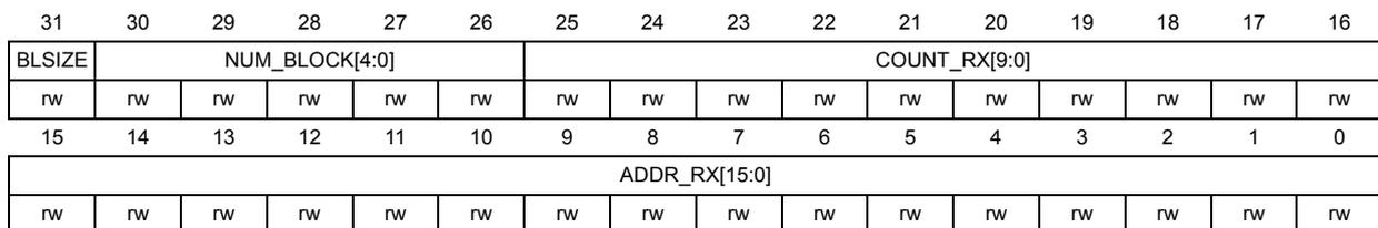
| 31 | 30 | 29 | 28 | 27 | 26 | 25 | 24 | 23 | 22 | 21 | 20 | 19 | 18 | 17 | 16 |
| BLSIZE | NUM_BLOCK[4:0] | COUNT_RX[9:0] | |||||||||||||
| rw | rw | rw | rw | rw | rw | rw | rw | rw | rw | rw | rw | rw | rw | rw | rw |
| 15 | 14 | 13 | 12 | 11 | 10 | 9 | 8 | 7 | 6 | 5 | 4 | 3 | 2 | 1 | 0 |
| ADDR_RX[15:0] | |||||||||||||||
| rw | rw | rw | rw | rw | rw | rw | rw | rw | rw | rw | rw | rw | rw | rw | rw |
Bit 31 BLSIZE : Block size
This bit selects the size of memory block used to define the allocated buffer area.
- – If BLSIZE = 0, the memory block is 2-byte large, which is the minimum block allowed in a half-word wide memory. With this block size the allocated buffer size ranges from 2 to 62 bytes.
- – If BLSIZE = 1, the memory block is 32-byte large, which permits to reach the maximum packet length defined by USB specifications. With this block size the allocated buffer size theoretically ranges from 32 to 1024 bytes, which is the longest packet size allowed by USB standard specifications. However, the applicable size is limited by the available buffer memory.
Bits 30:26 NUM_BLOCK[4:0] : Number of blocks
These bits define the number of memory blocks allocated to this packet buffer. The actual amount of allocated memory depends on the BLSIZE value as illustrated in Table 168 .
Bits 25:16 COUNT_RX[9:0] : Reception byte count
These bits contain the number of bytes received by the endpoint/channel associated with the USB_CHEPnR register during the last OUT/SETUP transaction addressed to it.
Note: Although the application only needs to read this value, it is writable.
Bits 15:0 ADDR_RX[15:0] : Reception buffer address
These bits point to the starting address of the packet buffer, which contains the data received by the endpoint/channel associated with the USB_CHEPnR register at the next OUT/SETUP token addressed to it. Bits 1 and 0 must always be written as “00” since packet memory is word wide and all packet buffers must be word aligned.
29.7.4 Channel/endpoint transmit buffer descriptor n [alternate]
(USB_CHEP_RTXBD_n)
Address offset: \( 0x4 + 0x8 * n \) , ( \( n = 0 \) to \( 7 \) )
Reset value: 0xXXXX XXXX
This register description applies when corresponding CHEPnR register programs use of double buffering and activates transmit buffers (otherwise refer to previous register description).
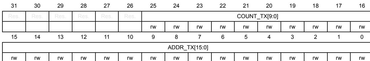
| 31 | 30 | 29 | 28 | 27 | 26 | 25 | 24 | 23 | 22 | 21 | 20 | 19 | 18 | 17 | 16 |
| Res. | Res. | Res. | Res. | Res. | Res. | COUNT_TX[9:0] | |||||||||
| rw | rw | rw | rw | rw | rw | rw | rw | rw | rw | ||||||
| 15 | 14 | 13 | 12 | 11 | 10 | 9 | 8 | 7 | 6 | 5 | 4 | 3 | 2 | 1 | 0 |
| ADDR_TX[15:0] | |||||||||||||||
| rw | rw | rw | rw | rw | rw | rw | rw | rw | rw | rw | rw | rw | rw | rw | rw |
Bits 31:26 Reserved, must be kept at reset value.
Bits 25:16 COUNT_TX[9:0] : Transmission byte count
These bits contain the number of bytes to be transmitted by the endpoint/channel associated with the USB_CHEPnR register at the next IN token addressed to it.
Bits 15:0 ADDR_TX[15:0] : Transmission buffer address
These bits point to the starting address of the packet buffer containing data to be transmitted by the endpoint/channel associated with the USB_CHEPnR register at the next IN token addressed to it. Bits 1 and 0 must always be written as “00” since packet memory is word wide and all packet buffers must be word aligned.
29.7.5 USBFSRAM register map
The table below provides the USB register map and reset values.
Table 169. USBFSRAM register map and reset values
| Offset | Register | 31 | 30 | 29 | 28 | 27 | 26 | 25 | 24 | 23 | 22 | 21 | 20 | 19 | 18 | 17 | 16 | 15 | 14 | 13 | 12 | 11 | 10 | 9 | 8 | 7 | 6 | 5 | 4 | 3 | 2 | 1 | 0 |
|---|---|---|---|---|---|---|---|---|---|---|---|---|---|---|---|---|---|---|---|---|---|---|---|---|---|---|---|---|---|---|---|---|---|
| 0x00 | USB_CHEP_TXRXBD_0 | Res. | Res. | Res. | Res. | Res. | Res. | COUNT_TX[9:0] | ADDR_TX[15:0] | ||||||||||||||||||||||||
| Reset value | X | X | X | X | X | X | X | X | X | X | X | X | X | X | X | X | X | X | X | X | X | X | X | X | X | X | |||||||
| 0x00 | USB_CHEP_TXRXBD_0 [alternate] | BLSIZE | NUM_BLOCK[4:0] | COUNT_RX[9:0] | ADDR_RX[15:0] | ||||||||||||||||||||||||||||
| Reset value | X | X | X | X | X | X | X | X | X | X | X | X | X | X | X | X | X | X | X | X | X | X | X | X | X | X | X | X | X | X | X | X | |
| 0x04 | USB_CHEP_RXTXBD_0 | BLSIZE | NUM_BLOCK[4:0] | COUNT_RX[9:0] | ADDR_RX[15:0] | ||||||||||||||||||||||||||||
| Reset value | X | X | X | X | X | X | X | X | X | X | X | X | X | X | X | X | X | X | X | X | X | X | X | X | X | X | X | X | X | X | X | X | |
| 0x04 | USB_CHEP_RXTXBD_0 [alternate] | Res. | Res. | Res. | Res. | Res. | Res. | COUNT_TX[9:0] | ADDR_TX[15:0] | ||||||||||||||||||||||||
| Reset value | X | X | X | X | X | X | X | X | X | X | X | X | X | X | X | X | X | X | X | X | X | X | X | X | X | X | |||||||
| 0x08 | USB_CHEP_TXRXBD_1 | Res. | Res. | Res. | Res. | Res. | Res. | COUNT_TX[9:0] | ADDR_TX[15:0] | ||||||||||||||||||||||||
| Reset value | X | X | X | X | X | X | X | X | X | X | X | X | X | X | X | X | X | X | X | X | X | X | X | X | X | X | |||||||
| 0x08 | USB_CHEP_TXRXBD_1 [alternate] | BLSIZE | NUM_BLOCK[4:0] | COUNT_RX[9:0] | ADDR_RX[15:0] | ||||||||||||||||||||||||||||
| Reset value | X | X | X | X | X | X | X | X | X | X | X | X | X | X | X | X | X | X | X | X | X | X | X | X | X | X | X | X | X | X | X | X | |
| 0x0C | USB_CHEP_RXTXBD_1 | BLSIZE | NUM_BLOCK[4:0] | COUNT_RX[9:0] | ADDR_RX[15:0] | ||||||||||||||||||||||||||||
| Reset value | X | X | X | X | X | X | X | X | X | X | X | X | X | X | X | X | X | X | X | X | X | X | X | X | X | X | X | X | X | X | X | X | |
| 0x0C | USB_CHEP_RXTXBD_1 [alternate] | Res. | Res. | Res. | Res. | Res. | Res. | COUNT_TX[9:0] | ADDR_TX[15:0] | ||||||||||||||||||||||||
| Reset value | X | X | X | X | X | X | X | X | X | X | X | X | X | X | X | X | X | X | X | X | X | X | X | X | X | X | |||||||
| . | . | . | |||||||||||||||||||||||||||||||
| . | . | . | |||||||||||||||||||||||||||||||
| . | . | . | |||||||||||||||||||||||||||||||
| 0x38 | USB_CHEP_TXRXBD_7 | Res. | Res. | Res. | Res. | Res. | Res. | COUNT_TX[9:0] | ADDR_TX[15:0] | ||||||||||||||||||||||||
| Reset value | X | X | X | X | X | X | X | X | X | X | X | X | X | X | X | X | X | X | X | X | X | X | X | X | X | X | |||||||
| 0x38 | USB_CHEP_TXRXBD_7 [alternate] | BLSIZE | NUM_BLOCK[4:0] | COUNT_RX[9:0] | ADDR_RX[15:0] | ||||||||||||||||||||||||||||
| Reset value | X | X | X | X | X | X | X | X | X | X | X | X | X | X | X | X | X | X | X | X | X | X | X | X | X | X | X | X | X | X | X | X | |
| 0x3C | USB_CHEP_RXTXBD_7 | BLSIZE | NUM_BLOCK[4:0] | COUNT_RX[9:0] | ADDR_RX[15:0] | ||||||||||||||||||||||||||||
| Reset value | X | X | X | X | X | X | X | X | X | X | X | X | X | X | X | X | X | X | X | X | X | X | X | X | X | X | X | X | X | X | X | X | |
| 0x3C | USB_CHEP_RXTXBD_7 [alternate] | Res. | Res. | Res. | Res. | Res. | Res. | COUNT_TX[9:0] | ADDR_TX[15:0] | ||||||||||||||||||||||||
| Reset value | X | X | X | X | X | X | X | X | X | X | X | X | X | X | X | X | X | X | X | X | X | X | X | X | X | X | |||||||