8. General-purpose I/Os (GPIO)
8.1 Introduction
Each general-purpose I/O port has four 32-bit configuration registers (GPIOx_MODER, GPIOx_OTYPER, GPIOx_OSPEEDR and GPIOx_PUPDR), two 32-bit data registers (GPIOx_IDR and GPIOx_ODR) and a 32-bit set/reset register (GPIOx_BSRR). In addition all GPIOs have a 32-bit locking register (GPIOx_LCKR) and two 32-bit alternate function selection registers (GPIOx_AFRH and GPIOx_AFRL).
8.2 GPIO main features
- • Output states: push-pull or open drain + pull-up/down
- • Output data from output data register (GPIOx_ODR) or peripheral (alternate function output)
- • Speed selection for each I/O
- • Input states: floating, pull-up/down, I/O analog mode
- • Input data to input data register (GPIOx_IDR) or peripheral (alternate function input)
- • Bit set and reset register (GPIOx_BSRR) for bitwise write access to GPIOx_ODR
- • Locking mechanism (GPIOx_LCKR) provided to freeze the I/O port configurations
- • Analog function
- • Alternate function selection registers (at most 16 AFs possible per I/O)
- • Fast toggle capable of changing every two clock cycles
- • Highly flexible pin multiplexing allows the use of I/O pins as GPIOs or as one of several peripheral functions
8.3 GPIO functional description
Subject to the specific hardware characteristics of each I/O port listed in the datasheet, each port bit of the general-purpose I/O (GPIO) ports can be individually configured by software in several modes:
- • Input floating
- • Input pull-up
- • Input pull-down
- • Analog
- • Output open-drain with pull-up or pull-down capability
- • Output push-pull with pull-up or pull-down capability
- • Alternate function push-pull with pull-up or pull-down capability
- • Alternate function open-drain with pull-up or pull-down capability
Each I/O port bit is freely programmable, however the I/O port registers have to be accessed as 32-bit words, half-words or bytes. The purpose of the GPIOx_BSRR and GPIOx_BRR registers is to allow atomic read/modify accesses to any of the GPIOx_ODR registers. In this way, there is no risk of an IRQ occurring between the read and the modify access.
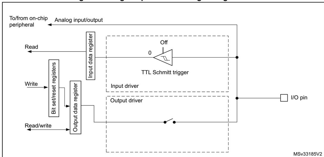
Figure 16 shows the basic structures of a standard I/O port bit. Table 38 gives the possible port bit configurations.
Figure 16. Basic structure of an I/O port bit
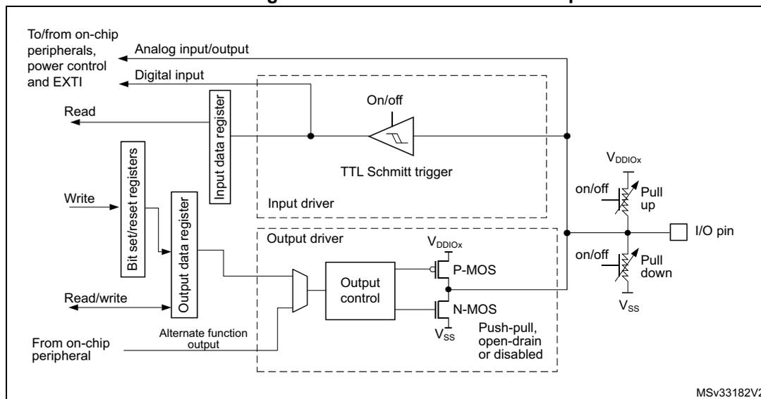
Table 38. Port bit configuration table (1)
| MODE(i) [1:0] | OTYPE(i) | OSPEED(i) [1:0] | PUPD(i) [1:0] | I/O configuration | ||
|---|---|---|---|---|---|---|
| 01 | 0 | SPEED [1:0] | 0 | 0 | GP output | PP |
| 0 | 0 | 1 | GP output | PP + PU | ||
| 0 | 1 | 0 | GP output | PP + PD | ||
| 0 | 1 | 1 | Reserved | |||
| 1 | 0 | 0 | GP output | OD | ||
| 1 | 0 | 1 | GP output | OD + PU | ||
| 1 | 1 | 0 | GP output | OD + PD | ||
| 1 | 1 | 1 | Reserved (GP output OD) | |||
| 10 | 0 | SPEED [1:0] | 0 | 0 | AF | PP |
| 0 | 0 | 1 | AF | PP + PU | ||
| 0 | 1 | 0 | AF | PP + PD | ||
| 0 | 1 | 1 | Reserved | |||
| 1 | 0 | 0 | AF | OD | ||
| 1 | 0 | 1 | AF | OD + PU | ||
| 1 | 1 | 0 | AF | OD + PD | ||
| 1 | 1 | 1 | Reserved | |||
| MODE(i) [1:0] | OTYPE(i) | OSPEED(i) [1:0] | PUPD(i) [1:0] | I/O configuration | |||
|---|---|---|---|---|---|---|---|
| 0 | 1 | 0 | 1 | ||||
| 00 | x | x | x | 0 | 0 | Input | Floating |
| x | x | x | 0 | 1 | Input | PU | |
| x | x | x | 1 | 0 | Input | PD | |
| x | x | x | 1 | 1 | Reserved (input floating) | ||
| 11 | x | x | x | 0 | 0 | Input/output | Analog |
| x | x | x | 0 | 1 | Reserved | ||
| x | x | x | 1 | 0 | |||
| x | x | x | 1 | 1 | |||
1. GP = general-purpose, PP = push-pull, PU = pull-up, PD = pull-down, OD = open-drain, AF = alternate function.
8.3.1 General-purpose I/O (GPIO)
During and just after reset, the alternate functions are not active and most of the I/O ports are configured in analog mode.
The debug pins are in AF pull-up/pull-down after reset:
- • PA14: SWCLK in pull-down
- • PA13: SWDIO in pull-up
Note: PA14 is shared with BOOT0 functionality. Caution is required as the debugging device can manipulate BOOT0 pin value.
When the pin is configured as output, the value written to the output data register (GPIOx_ODR) is output on the I/O pin. It is possible to use the output driver in push-pull mode or open-drain mode (only the low level is driven, high level is HI-Z).
The input data register (GPIOx_IDR) captures the data present on the I/O pin at every AHB clock cycle.
All GPIO pins have weak internal pull-up and pull-down resistors, which can be activated or not depending on the value in the GPIOx_PUPDR register.
The GPIO pins can operate as:
- • GPIO: output, input, or analog I/O, depending on the GPIOx_MODER register setting
- • Alternate function
The GPIOs with debug alternate functions are set to Alternate function mode upon reset.
- • Additional function
Available for some GPIO pins, the Additional function mode is set through the control registers of the corresponding functional block such as ADC, DAC, RTC, RCC, and PWR, regardless of the GPIOx_MODER register setting.
When an I/O is set in Additional function mode, it is recommended to set its corresponding GPIO multiplexer in the GPIOx_MODER register to Analog mode.
8.3.2 I/O pin alternate function multiplexer and mapping
Each functional block signal to connect on the device pins as alternate function is internally routed towards multiple GPIO pins. Each GPIO pin has a multiplexer with 16 positions (AF0 to AF15) controlled through the GPIOx_AFRH and GPIOx_AFRH registers, to select one of up to 16 alternate functions at a time. The alternate function selected for a GPIO pin is physically connected to the pin through GPIO mode multiplexer controlled by the GPIOx_MODER register.
Upon reset, the alternate function multiplexer on each GPIO is set to AF0 position.
This flexibility eases PCB routing and allows configuring small pin-count devices to match the application requirements.
The mapping of alternate function signals to GPIO alternate function multiplexers is detailed in the device datasheet.
To use an I/O in a given configuration, proceed as detailed in the following subsections.
Debug function
After each device reset, these pins are assigned as alternate function pins.
GPIO
Configure the desired I/O as output, input, or as an analog port, through the GPIOx_MODER register.
Peripheral alternate function
- • Connect the I/O to the desired AFx, through either GPIOx_AFRH or GPIOx_AFRH register.
- • Select the type, the pull-up or pull-down device, and the output speed via the GPIOx_OTYPER, GPIOx_PUPDR, and GPIOx_OSPEEDR register, respectively.
- • Configure the desired I/O as an alternate function, through the GPIOx_MODER register.
Cortex ® -M0+ alternate function (EVENTOUT)
The Cortex ® -M0+ output EVENTOUT signal can be used by configuring the I/O pin to output at the dedicated AF. An event can be signaled through the configured pin after executing the SEV instruction.
Additional functions
- • For the ADC, configure the desired I/O in analog mode, through the GPIOx_MODER register. Then configure the required function, through the ADC registers.
- • For the additional functions such as RTC, WKUPx, and oscillators, configure the required function through the related RTC, PWR, and RCC registers. These functions have priority over the configuration through the standard GPIO registers.
8.3.3 I/O port control registers
Each of the GPIO ports has four 32-bit memory-mapped control registers (GPIOx_MODER, GPIOx_OTYPER, GPIOx_OSPEEDR, GPIOx_PUPDR) to configure up to 16 I/Os. The GPIOx_MODER register is used to select the I/O mode (input, output, AF, analog). The GPIOx_OTYPER and GPIOx_OSPEEDR registers are used to select the output type (push-pull or open-drain) and speed. The GPIOx_PUPDR register is used to select the pull-up/pull-down whatever the I/O direction.
8.3.4 I/O port data registers
Each GPIO has two 16-bit memory-mapped data registers: input and output data registers (GPIOx_IDR and GPIOx_ODR). GPIOx_ODR stores the data to be output, it is read/write accessible. The data input through the I/O are stored into the input data register (GPIOx_IDR), a read-only register.
See Section 8.5.5: GPIO port input data register (GPIOx_IDR) (x = A, B, C, D, F) and Section 8.5.6: GPIO port output data register (GPIOx_ODR) (x = A, B, C, D, F) for the register descriptions.
8.3.5 I/O data bitwise handling
The bit set reset register (GPIOx_BSRR) is a 32-bit register which allows the application to set and reset each individual bit in the output data register (GPIOx_ODR). The bit set reset register has twice the size of GPIOx_ODR.
To each bit in GPIOx_ODR, correspond two control bits in GPIOx_BSRR: BS(i) and BR(i). When written to 1, bit BS(i) sets the corresponding ODR(i) bit. When written to 1, bit BR(i) resets the ODR(i) corresponding bit.
Writing any bit to 0 in GPIOx_BSRR does not have any effect on the corresponding bit in GPIOx_ODR. If there is an attempt to both set and reset a bit in GPIOx_BSRR, the set action takes priority.
Using the GPIOx_BSRR register to change the values of individual bits in GPIOx_ODR is a “one-shot” effect that does not lock the GPIOx_ODR bits. The GPIOx_ODR bits can always be accessed directly. The GPIOx_BSRR register provides a way of performing atomic bitwise handling.
There is no need for the software to disable interrupts when programming the GPIOx_ODR at bit level: it is possible to modify one or more bits in a single atomic AHB write access.
8.3.6 GPIO locking mechanism
It is possible to freeze the GPIO control registers by applying a specific write sequence to the GPIOx_LCKR register. The frozen registers are GPIOx_MODER, GPIOx_OTYPER, GPIOx_OSPEEDR, GPIOx_PUPDR, GPIOx_AFRL and GPIOx_AFRH.
To write the GPIOx_LCKR register, a specific write / read sequence has to be applied. When the right LOCK sequence is applied to bit 16 in this register, the value of LCKR[15:0] is used to lock the configuration of the I/Os (during the write sequence the LCKR[15:0] value must be the same). When the LOCK sequence has been applied to a port bit, the value of the port bit can no longer be modified until the next MCU reset or peripheral reset. Each GPIOx_LCKR bit freezes the corresponding bit in the control registers (GPIOx_MODER, GPIOx_OTYPER, GPIOx_OSPEEDR, GPIOx_PUPDR, GPIOx_AFRL and GPIOx_AFRH).
The LOCK sequence (refer to Section 8.5.8: GPIO port configuration lock register (GPIOx_LCKR) ( \( x = A, B, C, D, F \) )) can only be performed using a word (32-bit long) access to the GPIOx_LCKR register due to the fact that GPIOx_LCKR bit 16 has to be set at the same time as the [15:0] bits.
For more details refer to LCKR register description in Section 8.5.8: GPIO port configuration lock register (GPIOx_LCKR) ( \( x = A, B, C, D, F \) ).
8.3.7 I/O alternate function input/output
When an I/O pin operates in Alternate function mode, the alternate function selected determines whether it acts as an input or as an output.
The pull-up/pull-down and output speed settings (via the GPIOx_OTYPER, GPIOx_PUPDR and GPIOx_OSPEEDER registers, respectively) remain effective.
8.3.8 External interrupt/wake-up lines
All ports have external interrupt capability. To use external interrupt lines, the given pin must not be configured in analog mode or being used as oscillator pin, so the input trigger is kept enabled.
Refer to Section 14: Extended interrupt and event controller (EXTI) .
8.3.9 Input configuration
When the I/O port is programmed as input:
- • The output buffer is disabled
- • The Schmitt trigger input is activated
- • The pull-up and pull-down resistors are activated depending on the value in the GPIOx_PUPDR register
- • The data present on the I/O pin are sampled into the input data register every AHB clock cycle
- • A read access to the input data register provides the I/O state
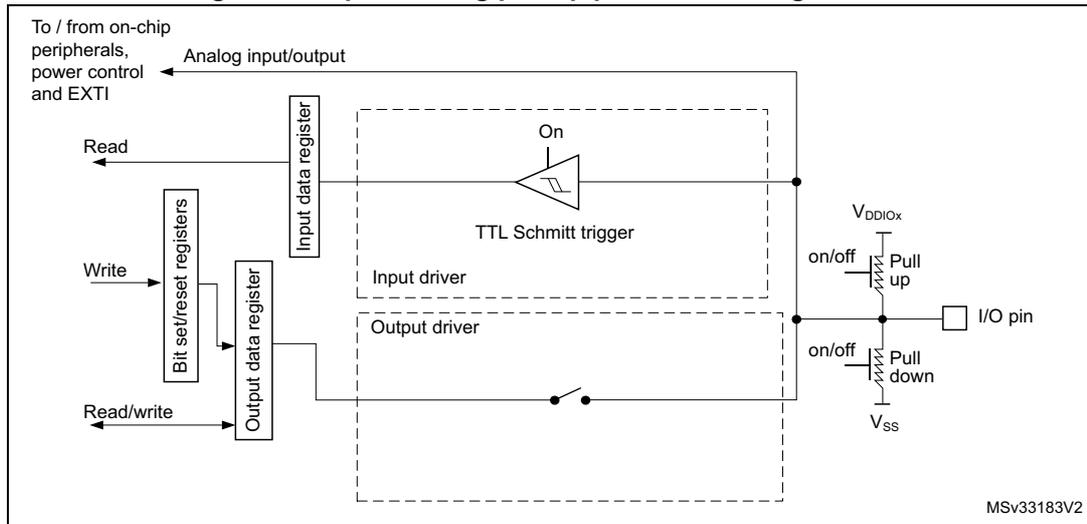
Figure 17 shows the input configuration of the I/O port bit.
Figure 17. Input floating/pull up/pull down configurations
8.3.10 Output configuration
When the I/O port is programmed as output:
- • The output buffer is enabled:
- – Open drain mode: A “0” in the Output register activates the N-MOS whereas a “1” in the Output register leaves the port in Hi-Z (the P-MOS is never activated)
- – Push-pull mode: A “0” in the Output register activates the N-MOS whereas a “1” in the Output register activates the P-MOS
- • The Schmitt trigger input is activated
- • The pull-up and pull-down resistors are activated depending on the value in the GPIOx_PUPDR register
- • The data present on the I/O pin are sampled into the input data register every AHB clock cycle
- • A read access to the input data register gets the I/O state
- • A read access to the output data register gets the last written value
Figure 18 shows the output configuration of the I/O port bit.
Figure 18. Output configuration
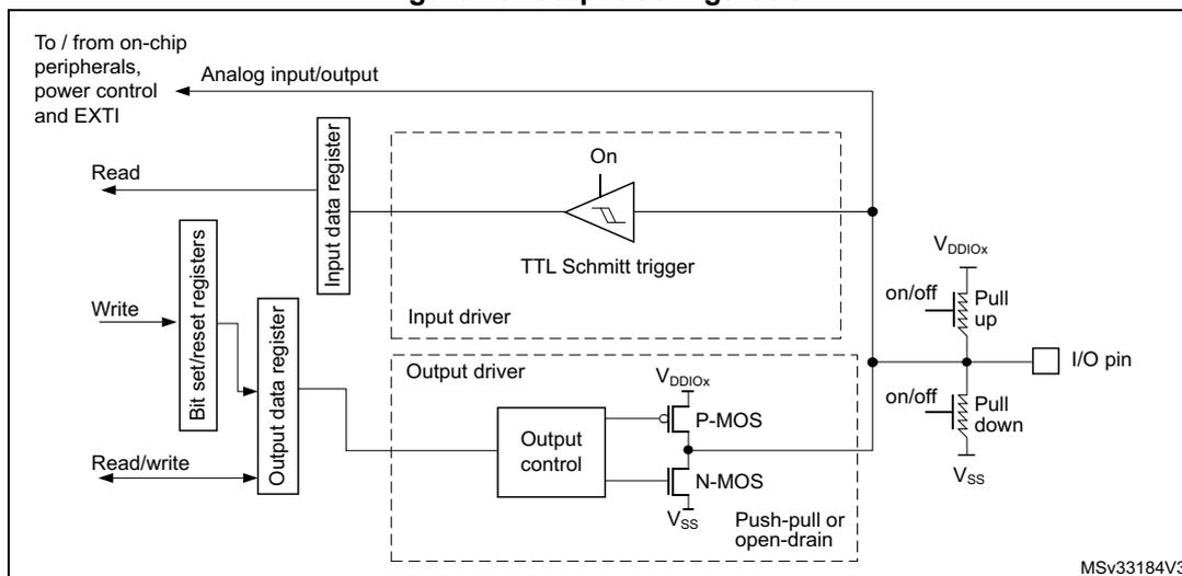
The diagram illustrates the internal circuitry of a GPIO pin configured for output. On the left, external connections include 'To / from on-chip peripherals, power control and EXTI' and 'Analog input/output'. The 'Input data register' is connected to the input driver, which contains a 'TTL Schmitt trigger' labeled 'On'. The 'Bit set/reset registers' and 'Output data register' are shown with 'Write' and 'Read/write' access paths. The 'Output data register' feeds into the 'Output control' block within the 'Output driver' section. This block drives a pair of transistors: a 'P-MOS' connected to \( V_{DDIOx} \) and an 'N-MOS' connected to \( V_{SS} \) . These transistors are labeled 'Push-pull or open-drain'. The output of the transistors is connected to the 'I/O pin'. Additionally, there are 'Pull up' and 'Pull down' resistors connected to the I/O pin, with 'on/off' switches, connected to \( V_{DDIOx} \) and \( V_{SS} \) respectively. The diagram is labeled 'MSv33184V3' in the bottom right corner.
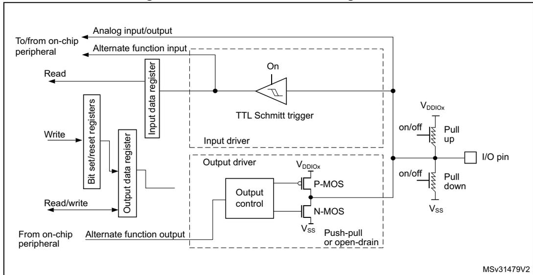
8.3.11 Alternate function configuration
When the I/O port is programmed as alternate function:
- • The output buffer can be configured in open-drain or push-pull mode
- • The output buffer is driven by the signals coming from the peripheral (transmitter enable and data)
- • The Schmitt trigger input is activated
- • The weak pull-up and pull-down resistors are activated or not depending on the value in the GPIOx_PUPDR register
- • The data present on the I/O pin are sampled into the input data register every AHB clock cycle
- • A read access to the input data register gets the I/O state
Figure 19 shows the Alternate function configuration of the I/O port bit.
Figure 19. Alternate function configuration-
8.3.12 Analog configuration
When the I/O port is programmed as analog configuration:
- • The output buffer is disabled
- • The Schmitt trigger input is deactivated, providing zero consumption for every analog value of the I/O pin. The output of the Schmitt trigger is forced to a constant value (0).
- • The weak pull-up and pull-down resistors are disabled by hardware
- • Read access to the input data register gets the value “0”
Figure 20 shows the high-impedance, analog configuration of the I/O port bits.
Figure 20. High impedance-analog configuration
8.3.13 Using the HSE or LSE oscillator pins as GPIOs
When the HSE or LSE oscillator is switched OFF (default state after reset), the related oscillator pins can be used as GPIOs.
When the HSE or LSE oscillator is switched ON (by setting the HSEON or LSEON bit of the RCC_CSR register), the oscillator takes control of its associated pins and the GPIO configuration of these pins has no effect.
When HSE or LSE oscillator is bypassed, its input pin is used as external clock input and its output pin is free for use as GPIO.
For the devices housed in 48-pin packages, the HSE and LSE oscillators have separate input and output pins (see HSE_NOT_REMAPPED bit of the FLASH option bytes). On packages with less than 48 pins, HSE and LSE oscillators have one common input pin OSCX_IN and one common output pin OSCX_OUT, which restricts their use to one at a time (the other must be disabled).
8.3.14 Low pin count package adjustment
Due to the restriction of some low pin count packages, multiple GPIOs are connected to the same I/O pins. The SYSCFG_CFGR3 register allows selecting which of them is active, to prevent conflicts.
8.3.15 Reset pin (PF2-NRST) in GPIO mode
The PF2-NRST pin can be configured as reset I/O or as a GPIO.
To configure PF2-NRST as a GPIO (input, output, AF, or analog I/O), set the NRST_MODE bitfield to GPIO mode in the FLASH option bytes. The new setting only takes effect upon the option byte loading (OBL) event following a reset. Until the reset release, PF2-NRST keeps acting as reset I/O.
The user must ensure that, upon power-on, the level on the NRST pin can exceed the minimum \( V_{IH(NRST)} \) level specified in the device datasheet. Otherwise, the device does not exit the power-on reset. This applies to any NRST configuration set through the NRST_MODE[1:0] bitfield, the GPIO mode inclusive.
When PF2-NRST acts as a GPIO, reset can only be triggered from one of the device internal reset sources and the reset signal cannot be output.
For further information on reset function, refer to the RCC section.
8.4 GPIO in low-power modes
Table 39. Effect of low-power modes on the GPIO
| Mode | Description |
|---|---|
| Sleep | No effect. GPIO (EXTI) interrupts cause the device to exit Sleep mode. |
| Stop | No effect. GPIO (EXTI) interrupts cause the device to exit Stop mode. |
Table 39. Effect of low-power modes on the GPIO (continued)
| Mode | Description |
|---|---|
| Standby | The GPIO digital interface is powered down and must be reinitialized after exiting Standby mode. Wake-up pins can be configured to cause the device to exit Standby mode. GPIO's are set to analog mode by hardware. Pull-up or pull-down device can individually be enabled through the PWR_PUCRx and PWR_PDCRx registers, respectively, to keep the I/Os at defined levels. |
| Shutdown | The GPIO digital interface is powered down and must be reinitialized after exiting Shutdown mode. Wake-up pins can be configured to cause the device to exit Shutdown mode. The GPIO's are set to analog mode by hardware. Pull-up or pull-down device can individually be enabled through the PWR_PUCRx and PWR_PDCRx registers, respectively, to keep the I/Os at defined levels. |
8.5 GPIO registers
This section gives a detailed description of the GPIO registers.
For a summary of register bits, register address offsets and reset values, refer to Table 40 .
The peripheral registers can be written in word, half word or byte mode.
Port D is only available on STM32C03xx products.
8.5.1 GPIO port mode register (GPIOx_MODER)
(x =A, B, C, D, F)
Address offset:0x00
Reset value: 0xEBFF FFFF (port A)
Reset value: 0xFFFF FFFF (ports other than A)
| 31 | 30 | 29 | 28 | 27 | 26 | 25 | 24 | 23 | 22 | 21 | 20 | 19 | 18 | 17 | 16 |
|---|---|---|---|---|---|---|---|---|---|---|---|---|---|---|---|
| MODE15[1:0] | MODE14[1:0] | MODE13[1:0] | MODE12[1:0] | MODE11[1:0] | MODE10[1:0] | MODE9[1:0] | MODE8[1:0] | ||||||||
| rw | rw | rw | rw | rw | rw | rw | rw | rw | rw | rw | rw | rw | rw | rw | rw |
| 15 | 14 | 13 | 12 | 11 | 10 | 9 | 8 | 7 | 6 | 5 | 4 | 3 | 2 | 1 | 0 |
| MODE7[1:0] | MODE6[1:0] | MODE5[1:0] | MODE4[1:0] | MODE3[1:0] | MODE2[1:0] | MODE1[1:0] | MODE0[1:0] | ||||||||
| rw | rw | rw | rw | rw | rw | rw | rw | rw | rw | rw | rw | rw | rw | rw | rw |
Bits 31:0 MODEy[1:0] : Port x configuration for I/O y (y = 15 to 0)
These bits are written by software to set the I/O to one of four operating modes.
00: Input
01: Output
10: Alternate function
11: Analog
8.5.2 GPIO port output type register (GPIOx_OTYPER)
(x = A, B, C, D, F)
Address offset: 0x04
Reset value: 0x0000 0000
| 31 | 30 | 29 | 28 | 27 | 26 | 25 | 24 | 23 | 22 | 21 | 20 | 19 | 18 | 17 | 16 |
|---|---|---|---|---|---|---|---|---|---|---|---|---|---|---|---|
| Res. | Res. | Res. | Res. | Res. | Res. | Res. | Res. | Res. | Res. | Res. | Res. | Res. | Res. | Res. | Res. |
| 15 | 14 | 13 | 12 | 11 | 10 | 9 | 8 | 7 | 6 | 5 | 4 | 3 | 2 | 1 | 0 |
| OT15 | OT14 | OT13 | OT12 | OT11 | OT10 | OT9 | OT8 | OT7 | OT6 | OT5 | OT4 | OT3 | OT2 | OT1 | OT0 |
| rw | rw | rw | rw | rw | rw | rw | rw | rw | rw | rw | rw | rw | rw | rw | rw |
Bits 31:16 Reserved, must be kept at reset value.
Bits 15:0 OTy : Port x configuration for I/O y (y = 15 to 0)
These bits are written by software to configure the I/O output type.
0: Output push-pull (reset state)
1: Output open-drain
8.5.3 GPIO port output speed register (GPIOx_OSPEEDR)
(x = A, B, C, D, F)
Address offset: 0x08
Reset value: 0x0C00 0000 (for port A)
Reset value: 0x0000 0000 (ports other than A)
| 31 | 30 | 29 | 28 | 27 | 26 | 25 | 24 | 23 | 22 | 21 | 20 | 19 | 18 | 17 | 16 |
|---|---|---|---|---|---|---|---|---|---|---|---|---|---|---|---|
| OSPEED15 [1:0] | OSPEED14 [1:0] | OSPEED13 [1:0] | OSPEED12 [1:0] | OSPEED11 [1:0] | OSPEED10 [1:0] | OSPEED9 [1:0] | OSPEED8 [1:0] | ||||||||
| rw | rw | rw | rw | rw | rw | rw | rw | rw | rw | rw | rw | rw | rw | rw | rw |
| 15 | 14 | 13 | 12 | 11 | 10 | 9 | 8 | 7 | 6 | 5 | 4 | 3 | 2 | 1 | 0 |
| OSPEED7 [1:0] | OSPEED6 [1:0] | OSPEED5 [1:0] | OSPEED4 [1:0] | OSPEED3 [1:0] | OSPEED2 [1:0] | OSPEED1 [1:0] | OSPEED0 [1:0] | ||||||||
| rw | rw | rw | rw | rw | rw | rw | rw | rw | rw | rw | rw | rw | rw | rw | rw |
Bits 31:0 OSPEEDy[1:0] : Port x configuration for I/O y (y = 15 to 0)
These bits are written by software to configure the I/O output speed.
00: Very low speed
01: Low speed
10: High speed
11: Very high speed
Note: Refer to the device datasheet for the frequency specifications and the power supply and load conditions for each speed..
The FT_c GPIOs cannot be set to high speed.
8.5.4 GPIO port pull-up/pull-down register (GPIOx_PUPDR)
(x = A, B, C, D, F)
Address offset: 0x0C
Reset value: 0x2400 0000 (for port A)
Reset value: 0x0000 0000 (ports other than A)
| 31 | 30 | 29 | 28 | 27 | 26 | 25 | 24 | 23 | 22 | 21 | 20 | 19 | 18 | 17 | 16 |
|---|---|---|---|---|---|---|---|---|---|---|---|---|---|---|---|
| PUPD15[1:0] | PUPD14[1:0] | PUPD13[1:0] | PUPD12[1:0] | PUPD11[1:0] | PUPD10[1:0] | PUPD9[1:0] | PUPD8[1:0] | ||||||||
| rw | rw | rw | rw | rw | rw | rw | rw | rw | rw | rw | rw | rw | rw | rw | rw |
| 15 | 14 | 13 | 12 | 11 | 10 | 9 | 8 | 7 | 6 | 5 | 4 | 3 | 2 | 1 | 0 |
| PUPD7[1:0] | PUPD6[1:0] | PUPD5[1:0] | PUPD4[1:0] | PUPD3[1:0] | PUPD2[1:0] | PUPD1[1:0] | PUPD0[1:0] | ||||||||
| rw | rw | rw | rw | rw | rw | rw | rw | rw | rw | rw | rw | rw | rw | rw | rw |
Bits 31:0 PUPDy[1:0] : Port x configuration I/O y (y = 15 to 0)
These bits are written by software to configure the I/O pull-up or pull-down
00: No pull-up, pull-down
01: Pull-up
10: Pull-down
11: Reserved
Note: On the same pin, this pull up/down must not be activated when a pull down/up is set through the PWR_PDCRx/PWR_PUCRx registers.
8.5.5 GPIO port input data register (GPIOx_IDR)
(x = A, B, C, D, F)
Address offset: 0x10
Reset value: 0x0000 XXXX
| 31 | 30 | 29 | 28 | 27 | 26 | 25 | 24 | 23 | 22 | 21 | 20 | 19 | 18 | 17 | 16 |
|---|---|---|---|---|---|---|---|---|---|---|---|---|---|---|---|
| Res. | Res. | Res. | Res. | Res. | Res. | Res. | Res. | Res. | Res. | Res. | Res. | Res. | Res. | Res. | Res. |
| 15 | 14 | 13 | 12 | 11 | 10 | 9 | 8 | 7 | 6 | 5 | 4 | 3 | 2 | 1 | 0 |
| ID15 | ID14 | ID13 | ID12 | ID11 | ID10 | ID9 | ID8 | ID7 | ID6 | ID5 | ID4 | ID3 | ID2 | ID1 | ID0 |
| r | r | r | r | r | r | r | r | r | r | r | r | r | r | r | r |
Bits 31:16 Reserved, must be kept at reset value.
Bits 15:0 IDy : Port x input data I/O y (y = 15 to 0)
These bits are read-only. They contain the input value of the corresponding I/O port.
8.5.6 GPIO port output data register (GPIOx_ODR)
(x = A, B, C, D, F)
Address offset: 0x14
Reset value: 0x0000 0000
| 31 | 30 | 29 | 28 | 27 | 26 | 25 | 24 | 23 | 22 | 21 | 20 | 19 | 18 | 17 | 16 |
|---|---|---|---|---|---|---|---|---|---|---|---|---|---|---|---|
| Res. | Res. | Res. | Res. | Res. | Res. | Res. | Res. | Res. | Res. | Res. | Res. | Res. | Res. | Res. | Res. |
| 15 | 14 | 13 | 12 | 11 | 10 | 9 | 8 | 7 | 6 | 5 | 4 | 3 | 2 | 1 | 0 |
| OD15 | OD14 | OD13 | OD12 | OD11 | OD10 | OD9 | OD8 | OD7 | OD6 | OD5 | OD4 | OD3 | OD2 | OD1 | OD0 |
| rw | rw | rw | rw | rw | rw | rw | rw | rw | rw | rw | rw | rw | rw | rw | rw |
Bits 31:16 Reserved, must be kept at reset value.
Bits 15:0 ODy : Port output data I/O y (y = 15 to 0)
These bits can be read and written by software.
Note: For atomic bit set/reset, the OD bits can be individually set and/or reset by writing to the GPIOx_BSR register (x = A, B, C, D, F).
8.5.7 GPIO port bit set/reset register (GPIOx_BSR)
(x = A, B, C, D, F)
Address offset: 0x18
Reset value: 0x0000 0000
| 31 | 30 | 29 | 28 | 27 | 26 | 25 | 24 | 23 | 22 | 21 | 20 | 19 | 18 | 17 | 16 |
|---|---|---|---|---|---|---|---|---|---|---|---|---|---|---|---|
| BR15 | BR14 | BR13 | BR12 | BR11 | BR10 | BR9 | BR8 | BR7 | BR6 | BR5 | BR4 | BR3 | BR2 | BR1 | BR0 |
| w | w | w | w | w | w | w | w | w | w | w | w | w | w | w | w |
| 15 | 14 | 13 | 12 | 11 | 10 | 9 | 8 | 7 | 6 | 5 | 4 | 3 | 2 | 1 | 0 |
| BS15 | BS14 | BS13 | BS12 | BS11 | BS10 | BS9 | BS8 | BS7 | BS6 | BS5 | BS4 | BS3 | BS2 | BS1 | BS0 |
| w | w | w | w | w | w | w | w | w | w | w | w | w | w | w | w |
Bits 31:16 BRy : Port x reset I/O y (y = 15 to 0)
These bits are write-only. A read operation always returns 0x0000.
0: No action on the corresponding ODRx bit
1: Resets the corresponding ODRx bit
Note: If both BSx and BRx are set, BSx has priority.
Bits 15:0 BSy : Port x set I/O y (y = 15 to 0)
These bits are write-only. A read operation always returns 0x0000.
0: No action on the corresponding ODRx bit
1: Sets the corresponding ODRx bit
8.5.8 GPIO port configuration lock register (GPIOx_LCKR)
(x = A, B, C, D, F)
This register is used to lock the configuration of the port bits when a correct write sequence is applied to bit 16 (LCKK). The value of bits [15:0] is used to lock the configuration of the GPIO. During the write sequence, the value of LCKR[15:0] must not change. When the LOCK sequence has been applied on a port bit, the value of this port bit can no longer be modified until the next MCU reset or peripheral reset.
Note: A specific write sequence is used to write to the GPIOx_LCKR register. Only word access (32-bit long) is allowed during this locking sequence.
Each lock bit freezes a specific configuration register (control and alternate function registers).
Address offset: 0x1C
Reset value: 0x0000 0000
| 31 | 30 | 29 | 28 | 27 | 26 | 25 | 24 | 23 | 22 | 21 | 20 | 19 | 18 | 17 | 16 |
|---|---|---|---|---|---|---|---|---|---|---|---|---|---|---|---|
| Res. | Res. | Res. | Res. | Res. | Res. | Res. | Res. | Res. | Res. | Res. | Res. | Res. | Res. | Res. | LCKK |
| rw | |||||||||||||||
| 15 | 14 | 13 | 12 | 11 | 10 | 9 | 8 | 7 | 6 | 5 | 4 | 3 | 2 | 1 | 0 |
| LCK15 | LCK14 | LCK13 | LCK12 | LCK11 | LCK10 | LCK9 | LCK8 | LCK7 | LCK6 | LCK5 | LCK4 | LCK3 | LCK2 | LCK1 | LCK0 |
| rw | rw | rw | rw | rw | rw | rw | rw | rw | rw | rw | rw | rw | rw | rw | rw |
Bits 31:17 Reserved, must be kept at reset value.
Bit 16 LCKK : Lock key
This bit can be read any time. It can only be modified using the lock key write sequence.
0: Port configuration lock key not active
1: Port configuration lock key active. The GPIOx_LCKR register is locked until the next MCU reset or peripheral reset.
LOCK key write sequence:
WR LCKR[16] = ‘1’ + LCKR[15:0]
WR LCKR[16] = ‘0’ + LCKR[15:0]
WR LCKR[16] = ‘1’ + LCKR[15:0]
RD LCKR
RD LCKR[16] = ‘1’ (this read operation is optional but it confirms that the lock is active)
Note: During the LOCK key write sequence, the value of LCK[15:0] must not change.
Any error in the lock sequence aborts the lock.
After the first lock sequence on any bit of the port, any read access on the LCKK bit returns ‘1’ until the next MCU reset or peripheral reset.
Bits 15:0 LCK[15:0] : Port x lock I/O pin y (y = 15 to 0)
These bits are read/write but can only be written when the LCKK bit is ‘0’.
0: Port configuration not locked
1: Port configuration locked
8.5.9 GPIO alternate function low register (GPIOx_AFRL)
(x = A, B, C, D, F)
Address offset: 0x20
Reset value: 0x0000 0000
| 31 | 30 | 29 | 28 | 27 | 26 | 25 | 24 | 23 | 22 | 21 | 20 | 19 | 18 | 17 | 16 |
|---|---|---|---|---|---|---|---|---|---|---|---|---|---|---|---|
| AFSEL7[3:0] | AFSEL6[3:0] | AFSEL5[3:0] | AFSEL4[3:0] | ||||||||||||
| rw | rw | rw | rw | rw | rw | rw | rw | rw | rw | rw | rw | rw | rw | rw | rw |
| 15 | 14 | 13 | 12 | 11 | 10 | 9 | 8 | 7 | 6 | 5 | 4 | 3 | 2 | 1 | 0 |
| AFSEL3[3:0] | AFSEL2[3:0] | AFSEL1[3:0] | AFSEL0[3:0] | ||||||||||||
| rw | rw | rw | rw | rw | rw | rw | rw | rw | rw | rw | rw | rw | rw | rw | rw |
Bits 31:0 AFSEL y [3:0] : Alternate function selection for port x pin y (y = 7 to 0)
These bits are written by software to configure alternate function I/Os
0000: AF0
0001: AF1
0010: AF2
0011: AF3
0100: AF4
0101: AF5
0110: AF6
0111: AF7
1000: AF8
1001: AF9
1010: AF10
1011: AF11
1100: AF12
1101: AF13
1110: AF14
1111: AF15
8.5.10 GPIO alternate function high register (GPIOx_AFRH)
(x = A, B, C, D, F)
Address offset: 0x24
Reset value: 0x0000 0000
| 31 | 30 | 29 | 28 | 27 | 26 | 25 | 24 | 23 | 22 | 21 | 20 | 19 | 18 | 17 | 16 |
|---|---|---|---|---|---|---|---|---|---|---|---|---|---|---|---|
| AFSEL15[3:0] | AFSEL14[3:0] | AFSEL13[3:0] | AFSEL12[3:0] | ||||||||||||
| rw | rw | rw | rw | rw | rw | rw | rw | rw | rw | rw | rw | rw | rw | rw | rw |
| 15 | 14 | 13 | 12 | 11 | 10 | 9 | 8 | 7 | 6 | 5 | 4 | 3 | 2 | 1 | 0 |
| AFSEL11[3:0] | AFSEL10[3:0] | AFSEL9[3:0] | AFSEL8[3:0] | ||||||||||||
| rw | rw | rw | rw | rw | rw | rw | rw | rw | rw | rw | rw | rw | rw | rw | rw |
Bits 31:0 AFSEL y [3:0] : Alternate function selection for port x, I/O y (y = 15 to 8)
These bits are written by software to configure alternate function I/Os
0000: AF0
0001: AF1
0010: AF2
0011: AF3
0100: AF4
0101: AF5
0110: AF6
0111: AF7
1000: AF8
1001: AF9
1010: AF10
1011: AF11
1100: AF12
1101: AF13
1110: AF14
1111: AF15
Address offset: 0x28
Reset value: 0x0000 0000
| 31 | 30 | 29 | 28 | 27 | 26 | 25 | 24 | 23 | 22 | 21 | 20 | 19 | 18 | 17 | 16 |
|---|---|---|---|---|---|---|---|---|---|---|---|---|---|---|---|
| Res. | Res. | Res. | Res. | Res. | Res. | Res. | Res. | Res. | Res. | Res. | Res. | Res. | Res. | Res. | Res. |
| 15 | 14 | 13 | 12 | 11 | 10 | 9 | 8 | 7 | 6 | 5 | 4 | 3 | 2 | 1 | 0 |
| BR15 | BR14 | BR13 | BR12 | BR11 | BR10 | BR9 | BR8 | BR7 | BR6 | BR5 | BR4 | BR3 | BR2 | BR1 | BR0 |
| w | w | w | w | w | w | w | w | w | w | w | w | w | w | w | w |
Bits 31:16 Reserved, must be kept at reset value.
Bits 15:0 BRy : Port x reset I/O y (y = 15 to 0)These bits are write-only. A read operation always returns 0x0000.
0: No action on the corresponding ODx bit
1: Reset the corresponding ODx bit
8.5.12 GPIO register map
The following table gives the GPIO register map and reset values.
Table 40. GPIO register map and reset values
| Offset | Register name | 31 | 30 | 29 | 28 | 27 | 26 | 25 | 24 | 23 | 22 | 21 | 20 | 19 | 18 | 17 | 16 | 15 | 14 | 13 | 12 | 11 | 10 | 9 | 8 | 7 | 6 | 5 | 4 | 3 | 2 | 1 | 0 | |
|---|---|---|---|---|---|---|---|---|---|---|---|---|---|---|---|---|---|---|---|---|---|---|---|---|---|---|---|---|---|---|---|---|---|---|
| 0x00 | GPIOx_MODER (x = A, B, C, D, F) | MODE15[1:0] | MODE14[1:0] | MODE13[1:0] | MODE12[1:0] | MODE11[1:0] | MODE10[1:0] | MODE9[1:0] | MODE8[1:0] | MODE7[1:0] | MODE6[1:0] | MODE5[1:0] | MODE4[1:0] | MODE3[1:0] | MODE2[1:0] | MODE1[1:0] | MODE0[1:0] | |||||||||||||||||
| Reset value (port A) | 1 | 1 | 1 | 0 | 1 | 0 | 1 | 1 | 1 | 1 | 1 | 1 | 1 | 1 | 1 | 1 | 1 | 1 | 1 | 1 | 1 | 1 | 1 | 1 | 1 | 1 | 1 | 1 | 1 | 1 | 1 | 1 | ||
| Reset value (ports other than A) | 1 | 1 | 1 | 1 | 1 | 1 | 1 | 1 | 1 | 1 | 1 | 1 | 1 | 1 | 1 | 1 | 1 | 1 | 1 | 1 | 1 | 1 | 1 | 1 | 1 | 1 | 1 | 1 | 1 | 1 | 1 | 1 | ||
| 0x04 | GPIOx_OTYPER (x = A, B, C, D, F) | Res | Res | Res | Res | Res | Res | Res | Res | Res | Res | Res | Res | Res | Res | Res | Res | OT15 | OT14 | OT13 | OT12 | OT11 | OT10 | OT9 | OT8 | OT7 | OT6 | OT5 | OT4 | OT3 | OT2 | OT1 | OT0 | |
| Reset value | 0 | 0 | 0 | 0 | 0 | 0 | 0 | 0 | 0 | 0 | 0 | 0 | 0 | 0 | 0 | 0 | ||||||||||||||||||
| 0x08 | GPIOx_OSPEEDR (x = A, B, C, D, F) | OSPEED15[1:0] | OSPEED14[1:0] | OSPEED13[1:0] | OSPEED12[1:0] | OSPEED11[1:0] | OSPEED10[1:0] | OSPEED9[1:0] | OSPEED8[1:0] | OSPEED7[1:0] | OSPEED6[1:0] | OSPEED5[1:0] | OSPEED4[1:0] | OSPEED3[1:0] | OSPEED2[1:0] | OSPEED1[1:0] | OSPEED0[1:0] | |||||||||||||||||
| Reset value (port A) | 0 | 0 | 0 | 0 | 1 | 1 | 0 | 0 | 0 | 0 | 0 | 0 | 0 | 0 | 0 | 0 | 0 | 0 | 0 | 0 | 0 | 0 | 0 | 0 | 0 | 0 | 0 | 0 | 0 | 0 | 0 | 0 | ||
| Reset value (ports other than A) | 0 | 0 | 0 | 0 | 0 | 0 | 0 | 0 | 0 | 0 | 0 | 0 | 0 | 0 | 0 | 0 | 0 | 0 | 0 | 0 | 0 | 0 | 0 | 0 | 0 | 0 | 0 | 0 | 0 | 0 | 0 | 0 | ||
| 0x0C | GPIOx_PUPDR (x = A, B, C, D, F) | PUPD15[1:0] | PUPD14[1:0] | PUPD13[1:0] | PUPD12[1:0] | PUPD11[1:0] | PUPD10[1:0] | PUPD9[1:0] | PUPD8[1:0] | PUPD7[1:0] | PUPD6[1:0] | PUPD5[1:0] | PUPD4[1:0] | PUPD3[1:0] | PUPD2[1:0] | PUPD1[1:0] | PUPD0[1:0] | |||||||||||||||||
| Reset value (port A) | 0 | 0 | 1 | 0 | 0 | 1 | 0 | 0 | 0 | 0 | 0 | 0 | 0 | 0 | 0 | 0 | 0 | 0 | 0 | 0 | 0 | 0 | 0 | 0 | 0 | 0 | 0 | 0 | 0 | 0 | 0 | 0 | ||
| Reset value (ports other than A) | 0 | 0 | 0 | 0 | 0 | 0 | 0 | 0 | 0 | 0 | 0 | 0 | 0 | 0 | 0 | 0 | 0 | 0 | 0 | 0 | 0 | 0 | 0 | 0 | 0 | 0 | 0 | 0 | 0 | 0 | 0 | 0 | ||
| 0x10 | GPIOx_IDR (x = A, B, C, D, F) | Res | Res | Res | Res | Res | Res | Res | Res | Res | Res | Res | Res | Res | Res | Res | Res | ID15 | ID14 | ID13 | ID12 | ID11 | ID10 | ID9 | ID8 | ID7 | ID6 | ID5 | ID4 | ID3 | ID2 | ID1 | ID0 | |
| Reset value | x | x | x | x | x | x | x | x | x | x | x | x | x | x | x | x | ||||||||||||||||||
| 0x14 | GPIOx_ODR (x = A, B, C, D, F) | Res | Res | Res | Res | Res | Res | Res | Res | Res | Res | Res | Res | Res | Res | Res | Res | OD15 | OD14 | OD13 | OD12 | OD11 | OD10 | OD9 | OD8 | OD7 | OD6 | OD5 | OD4 | OD3 | OD2 | OD1 | OD0 | |
| Reset value | 0 | 0 | 0 | 0 | 0 | 0 | 0 | 0 | 0 | 0 | 0 | 0 | 0 | 0 | 0 | 0 | ||||||||||||||||||
| 0x18 | GPIOx_BSRR (x = A, B, C, D, F) | BR15 | BR14 | BR13 | BR12 | BR11 | BR10 | BR9 | BR8 | BR7 | BR6 | BR5 | BR4 | BR3 | BR2 | BR1 | BR0 | BS15 | BS14 | BS13 | BS12 | BS11 | BS10 | BS9 | BS8 | BS7 | BS6 | BS5 | BS4 | BS3 | BS2 | BS1 | BS0 | |
| Reset value | 0 | 0 | 0 | 0 | 0 | 0 | 0 | 0 | 0 | 0 | 0 | 0 | 0 | 0 | 0 | 0 | 0 | 0 | 0 | 0 | 0 | 0 | 0 | 0 | 0 | 0 | 0 | 0 | 0 | 0 | 0 | 0 | ||
| 0x1C | GPIOx_LCKR (x = A, B, C, D, F) | Res | Res | Res | Res | Res | Res | Res | Res | Res | Res | Res | Res | Res | Res | Res | Res | LCKK | LCK15 | LCK14 | LCK13 | LCK12 | LCK11 | LCK10 | LCK9 | LCK8 | LCK7 | LCK6 | LCK5 | LCK4 | LCK3 | LCK2 | LCK1 | LCK0 |
| Reset value | 0 | 0 | 0 | 0 | 0 | 0 | 0 | 0 | 0 | 0 | 0 | 0 | 0 | 0 | 0 | 0 | ||||||||||||||||||
| 0x20 | GPIOx_AFRL (x = A, B, C, D, F) | AFSEL7 [3:0] | AFSEL6 [3:0] | AFSEL5 [3:0] | AFSEL4 [3:0] | AFSEL3 [3:0] | AFSEL2 [3:0] | AFSEL1 [3:0] | AFSEL0 [3:0] | |||||||||||||||||||||||||
| Reset value | 0 | 0 | 0 | 0 | 0 | 0 | 0 | 0 | 0 | 0 | 0 | 0 | 0 | 0 | 0 | 0 | 0 | 0 | 0 | 0 | 0 | 0 | 0 | 0 | 0 | 0 | 0 | 0 | 0 | 0 | 0 | 0 | ||
| 0x24 | GPIOx_AFRH (x = A, B, C, D, F) | AFSEL15 [3:0] | AFSEL14 [3:0] | AFSEL13 [3:0] | AFSEL12 [3:0] | AFSEL11 [3:0] | AFSEL10 [3:0] | AFSEL9 [3:0] | AFSEL8 [3:0] | |||||||||||||||||||||||||
| Reset value | 0 | 0 | 0 | 0 | 0 | 0 | 0 | 0 | 0 | 0 | 0 | 0 | 0 | 0 | 0 | 0 | 0 | 0 | 0 | 0 | 0 | 0 | 0 | 0 | 0 | 0 | 0 | 0 | 0 | 0 | 0 | 0 | ||
| 0x28 | GPIOx_BRR (x = A, B, C, D, F) | Res | Res | Res | Res | Res | Res | Res | Res | Res | Res | Res | Res | Res | Res | Res | Res | BR15 | BR14 | BR13 | BR12 | BR11 | BR10 | BR9 | BR8 | BR7 | BR6 | BR5 | BR4 | BR3 | BR2 | BR1 | BR0 | |
| Reset value | 0 | 0 | 0 | 0 | 0 | 0 | 0 | 0 | 0 | 0 | 0 | 0 | 0 | 0 | 0 | 0 | ||||||||||||||||||
Refer to Section 2.2 on page 45 for the register boundary addresses.