5. Power control (PWR)
5.1 Power supplies and voltage references
The devices are powered through the VDD/VDDA pin. Internally, the power is delivered through the V DD power line supplying the internal resources in the V DD power domain and the flash memory, the V DDA power line supplying the ADC, and the V DDIO1 and V DDIO2 (V DDIO2 only available on STM32C071xx) power lines supplying the I/O ring.
Through the V CORE power line, the voltage regulator supplies the resources in the V CORE power domain including the core, SRAM and digital peripherals, the RTC domain and the flash memory.
Refer to the following figure and to the device datasheets for further information.
Figure 5. Power supply overview
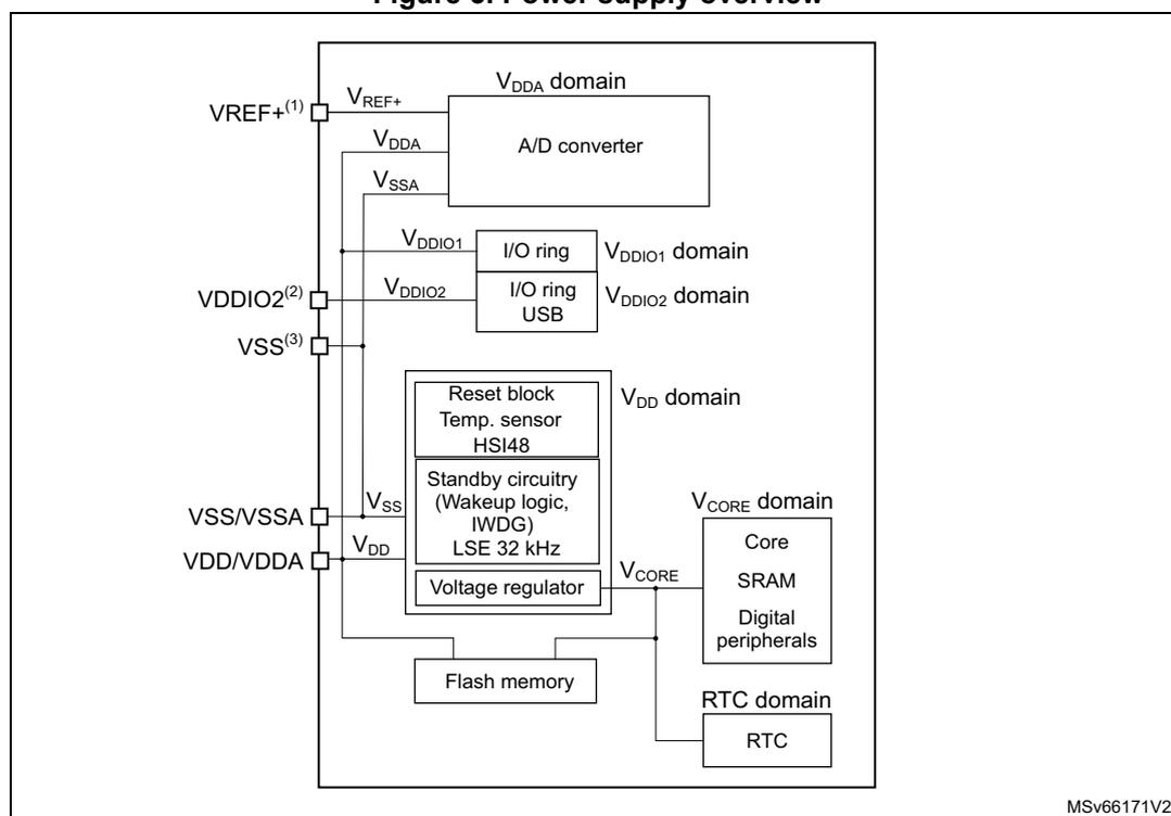
The diagram shows the internal power architecture of the microcontroller. On the left, external pins are listed: VREF +(1) , VDDIO2 (2) , VSS (3) , VSS/VSSA, and VDD/VDDA. These pins connect to various internal power domains and blocks:
- VREF +(1) connects to the V REF+ input of the V DDA domain (containing an A/D converter ).
- VDDIO2 (2) connects to the V DDIO2 input of the V DDIO2 domain (containing an I/O ring USB ).
- VSS (3) and VSS/VSSA connect to the V SS input of the V DD domain (containing a Reset block , Temp. sensor HSI48 , and Standby circuitry (Wakeup logic, IWDG, LSE 32 kHz) ).
- VDD/VDDA connects to the V DD input of the V DD domain and the V CORE input of the V CORE domain (containing Core , SRAM , and Digital peripherals ).
- The V DD domain also includes a Voltage regulator which supplies the V CORE domain and the RTC domain (containing RTC ).
- The V DDA domain also includes V DDA and V SSA inputs.
- The V DDIO1 domain (containing an I/O ring ) is connected to the V DDIO1 input.
- Flash memory is connected to the V DD and V CORE lines.
MSv66171V/2
- 1. Internally connected to VDD/VDDA pin on packages without VREF+ pin.
- 2. Internally connected to VDD/VDDA pin on packages without VDDIO2 pin.
- 3. Internally connected to VSS/VSSA pin on packages without VSS pin.
Note: VDDIO2 and VSS pins are only available on some packages. VDDIO2 is only available on STM32C071xx.
5.1.1 ADC reference voltage
V REF+ defines the full-scale ADC input signal level. On packages with VREF+ input pin, the V REF+ voltage reference is supplied externally, which allows increasing the ADC resolution (voltage per step) and reducing the noise. Refer to the device datasheets for the allowed V REF+ range.
5.1.2 Voltage regulator
When enabled, the voltage regulator provides the \( V_{\text{CORE}} \) supply voltage to the \( V_{\text{CORE}} \) domain.
The regulator is enabled upon reset and remains enabled as long as the device operates in Run, Sleep, or Stop mode.
In Standby and Shutdown modes, the regulator is disabled and the \( V_{\text{CORE}} \) domain is not powered. As a consequence, the SRAM and register contents are lost.
5.2 Power supply supervisor
5.2.1 Power-on reset (POR) / power-down reset (PDR) / brown-out reset (BOR)
The device features an integrated power-on reset (POR) / power-down reset (PDR), coupled with a brown-out reset (BOR) circuitry. The POR/PDR is active in all power modes. The BOR can be enabled or disabled only through option bytes. It is not available in Shutdown mode.
When the BOR is enabled, four BOR levels can be selected through option bytes, with independent configuration for rising and falling thresholds. During power-on, the BOR keeps the device under reset until the \( V_{\text{DD}} \) supply voltage reaches the specified BOR rising threshold ( \( V_{\text{BORRx}} \) ). At this point, the device reset is released and the system can start. During power-down, when \( V_{\text{DD}} \) drops below the selected BOR falling threshold ( \( V_{\text{BORFx}} \) ), the device is put under reset again.
Warning: It is not allowed to configure BOR falling threshold ( \( V_{\text{BORFx}} \) ) to a value higher than BOR rising threshold ( \( V_{\text{BORRx}} \) ).
Figure 6. POR, PDR, and BOR thresholds
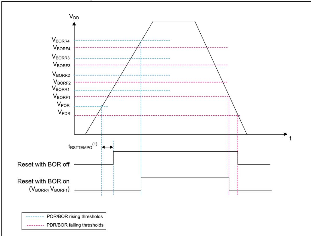
The figure is a timing diagram illustrating the relationship between supply voltage ( \( V_{DD} \) ), Brown-out Reset (BOR) thresholds, and the system reset signal over time ( \( t \) ).
- Top Graph:
The y-axis represents
\(
V_{DD}
\)
and the x-axis represents time
\(
t
\)
. The
\(
V_{DD}
\)
signal is shown as a trapezoidal waveform. Several horizontal threshold levels are marked on the y-axis:
- \( V_{BORR4} \) , \( V_{BORR3} \) , \( V_{BORR2} \) , \( V_{BORR1} \) (Blue dashed lines, representing rising thresholds)
- \( V_{BORF4} \) , \( V_{BORF3} \) , \( V_{BORF2} \) , \( V_{BORF1} \) (Pink dashed lines, representing falling thresholds)
- \( V_{POR} \) (Blue dashed line)
- \( V_{PDR} \) (Pink dashed line)
- Reset Signals:
Below the voltage graph, two reset signal waveforms are shown:
- Reset with BOR off: This signal goes low (active) when \( V_{DD} \) crosses the \( V_{POR} \) threshold and returns high when \( V_{DD} \) crosses the \( V_{PDR} \) threshold.
- Reset with BOR on ( \( V_{BORR4} \) \( V_{BORF1} \) ): This signal goes low when \( V_{DD} \) crosses the \( V_{POR} \) threshold and returns high when \( V_{DD} \) crosses the \( V_{BORF1} \) threshold.
- Reset Temporization: A horizontal double-headed arrow labeled \( t_{RSTTEMPO}^{(1)} \) indicates the time interval between the start of the reset (when \( V_{DD} \) crosses \( V_{POR} \) ) and the start of the BOR reset (when \( V_{DD} \) crosses \( V_{BORR4} \) ).
- Legend:
- Blue dashed line: POR/BOR rising thresholds
- Pink dashed line: PDR/BOR falling thresholds
- 1. The reset temporization \( t_{RSTTEMPO} \) starts when \( V_{DD} \) crosses \( V_{POR} \) threshold, indifferently from the configuration of the BOR Option bits.
For more details on the brown-out reset thresholds, refer to the electrical characteristics section in the datasheet.
5.3 Operating modes
The device has a full-operating mode called Run mode and several low-power modes allowing substantial power saving.
Upon a system or a power-on reset, the device starts operating in Run mode.
Sleep, Stop, Standby, and Shutdown low-power modes are available to save power when there is no need for the CPU to execute instructions, for example when waiting for an external event.
Different low-power modes offer different trade-offs between power consumption, startup speed and wake-up possibilities. While the Sleep mode offers the highest agility at cost of the least power saving, the Shutdown mode provides the lowest power consumption at cost of slower wake-up and absence of power supply monitoring and BOR/PDR. The Standby mode, compared to Shutdown, keeps the LSI oscillator, the IWDG and the voltage monitoring active, at cost of a slightly greater power consumption. The Stop mode keeps low-speed clocks and peripherals, as well as GPIOs active.
Refer to Table 27: Device resources enabled in different operating modes and Table 29: Low-power mode exit overview for all details.
The device can transit from Run mode to any of the low-power modes and from any low-power operating mode to Run mode. Transiting from one low-power mode to another is not possible. Refer to the following figure.
Figure 7. Low-power mode transit diagram
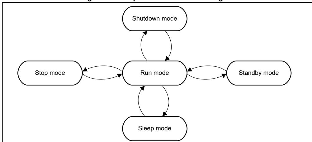
graph TD; Run([Run mode]) <--> Shutdown([Shutdown mode]); Run <--> Stop([Stop mode]); Run <--> Standby([Standby mode]); Run <--> Sleep([Sleep mode]);
The diagram illustrates the power mode transitions for the device. A central 'Run mode' oval is connected to four other ovals: 'Shutdown mode' (top), 'Standby mode' (right), 'Sleep mode' (bottom), and 'Stop mode' (left). Each connection is represented by a double-headed arrow, indicating that the device can transition from Run mode to any of these low-power modes and back again. There are no direct connections between the low-power modes themselves.
The following table gives an overview of the device resources available in each operating mode and their capability to wake the device up from a low-power mode to Run mode. Refer to the table footnotes for complementary information.
Table 27. Device resources enabled in different operating modes
| Function | Operating mode (1) | |||||||
|---|---|---|---|---|---|---|---|---|
| Run | Sleep | Stop (2) | Standby (2) | Shutdown (2) | ||||
| CPU | Y | - | - | - | - | - | - | - |
| Flash memory | Y | Y | A (3) | - | - | - | - | - |
| SRAM | Y | Y | U | - | - | - | - | - |
| V CORE supply (4) | Y | Y | Y | - | - | - | - | - |
| BOR/POR/PDR | O | O | U | U | U | U | _(5) | - |
| NRST | Y | Y | Y | Y | Y | Y | Y | Y |
| DMA/DMAMUX | O | U | - | - | - | - | - | - |
| HSI48 | Y | U (6) | _(6) | - | - | - | - | - |
| HSIUSB48 | Y | U | - | - | - | - | - | - |
| HSE | O | U | - | - | - | - | - | - |
| LSI | O | U | U | - | U | - | - | - |
| LSE | O | U | U | - | - | - | - | - |
| CSS | O | U | - | - | - | - | - | - |
| CSS on LSE | O | U | U | O | - | - | - | - |
| RTC / Auto wake-up | O | U | U | O | - | - | - | - |
| USART1 | O | U (7) | U (7) | O (7) | - | - | - | - |
| USART2/3/4 | O | U (7) | - | - | - | - | - | - |
| I2C1 | O | U (8) | U (8) | O (8) | - | - | - | - |
| I2C2 | O | U | - | - | - | - | - | - |
| SPI1, SPI2 | O | U | - | - | - | - | - | - |
| ADC | O | U | _(9) | - | - | - | - | - |
| Temperature sensor | O | U | _(9) | - | - | - | - | - |
| TIMx | O | U | - | - | - | - | - | - |
| IWDG | O | U | U | O | U | O | - | - |
| WWDG | O | U | - | - | - | - | - | - |
| SysTick timer | O | U | - | - | - | - | - | - |
Table 27. Device resources enabled in different operating modes (continued)
| Function | Operating mode (1) | |||||||
|---|---|---|---|---|---|---|---|---|
| Run | Sleep | Stop (2) | Standby (2) | Shutdown (2) | ||||
| CRC | O | U | - | - | - | - | - | - |
| GPIOs | O | U | U | O | (10) | (11) | (10) | (11) |
| Individual peripheral clocks to peripherals | O | A (12) | A (12) | - | - | - | - | - |
| USB | O | O | - | O (13) | - | - | - | - |
| FDCAN1 | O | O | - | - | - | - | - | - |
- 1. Y = (yes): resource enabled upon reset and upon wake-up from Stop, Standby, and Shutdown; O = (optional): resource disabled by default, and possible to enable by software; U = (unchanged): resource kept in the same operating state as before low-power mode entry; A = (automatic): resource can be set for automatic disable/power-down upon transiting to low-power mode; - = resource not available / without wake-up capability (grayed-out columns)
- 2. The grayed-out column indicates the capability of the resource to wake the device up from a low-power mode.
- 3. Possibility of automatic power-down.
- 4. When not available (voltage regulator disabled), the SRAM and register contents are lost.
- 5. The supply voltage monitoring is disabled and the product behavior is not guaranteed in case of a power voltage drop.
- 6. When the HSI48 is off, peripherals with wake-up capability, such as I2C1, can wake the HSI48 oscillator up to allow temporary operation to assess the device wake-up condition such as I 2 C address match, then stop HSI48 if the wake-up condition is not met, or wake the device up if it is met. When the HSI48 is restarted by a peripheral with wake-up capability, during the low-power mode it only delivers clock to that peripheral.
- 7. USART reception is functional in Sleep and Stop mode. It generates a wake-up interrupt on START, address match, or received frame event. The peripheral has the capability to restart the HSI48 oscillator to assess the address match and received frame event device wake-up conditions.
- 8. I 2 C address detection is functional in Sleep and Stop mode. It generates a wake-up interrupt on address match. The peripheral has the capability to restart the HSI48 oscillator to assess the address match event device wake-up condition.
- 9. Keeps consuming idle current unless disabled prior to entering Stop mode.
- 10. I/Os can be configured to keep, in Standby and Shutdown mode, internal pull-up or pull-down, or to float. Refer to PUCRx and PDCRx registers and the APC bit of the PWR_CR3 register. This configuration is kept when exiting Standby mode but it is lost when exiting Shutdown mode.
- 11. WKUPx I/Os (up to five, depending on the package), with wake-up from Standby/Shutdown mode capability.
- 12. Through the RCC_AHBSMENR and RCC_APBMSMENRx registers, the software can configure the individual peripheral clocks to automatically disable upon entering Sleep and Stop modes.
- 13. USB bus state monitoring is functional in Stop mode. It generates a wake-up interrupt if the resume from the USB suspend is detected.
5.3.1 Power saving in run mode
The power consumption in Run mode can be reduced through selecting a system clock with lower frequency, scaling down the system clock frequency, disabling unused peripherals and/or stopping their clocks (peripheral clock gating).
Slowing down system clocks
The SYSCLK, HCLK, and PCLK clock frequencies can be reduced with prescalers controlled through prescaler registers. Their settings also apply to the Sleep mode.
For more details, refer to Section 6.4.3: RCC clock configuration register (RCC_CFGR) .
Peripheral clock gating
The HCLK and PCLK to individual peripherals and memories can be stopped (clock gating) at any time to reduce the power consumption.
The RCC_AHBENR and RCC_APBENRx registers enable or disable individual clocks to peripherals (clock gating). To further reduce the power consumption in Sleep/Stop modes, the peripheral clocks can be disabled prior to executing the WFI or WFE instructions.
Disabling the peripherals clocks in Sleep/Stop modes can be performed automatically, by clearing the corresponding bit of the RCC_AHBSMENR and RCC_APBSMENRx registers.
5.3.2 Low-power modes
The device features the following low-power modes:
- •
Sleep mode
CPU clock is off, all peripherals including Cortex ® -M0+ core peripherals such as NVIC and SysTick can run and wake up the CPU when an interrupt or an event occurs. To further reduce the power consumption in Sleep mode, the peripheral clocks can be disabled prior to executing the WFI or WFE instructions. This can also be done automatically, by configuring RCC_AHBSMENR and RCC_APBSMENRx registers. If disabled before entering Sleep mode, HSI48 can be restarted by a peripheral with wake-up capability requiring HSI48. - •
Stop mode
SRAM and register contents are retained. HSE and HSI48 stop. HSI48 can be restarted by a peripheral with wake-up capability requiring HSI48. The LSI and LSE oscillators can be kept running. The RTC can remain active (Stop mode with RTC, Stop mode without RTC). The event of exiting Stop mode enables the HSI48 oscillator and selects HSISYS as system clock. - •
Standby mode
V CORE domain is powered off and the SRAM and register contents lost, except PWR control register 3 (PWR_CR3) and PWR backup x register (PWR_BKPxR) . All clocks in the V CORE domain are stopped and the HSI48 and HSE oscillators disabled. The IWDG and the LSI oscillator can be kept running. The event of exiting Standby mode enables the HSI48 oscillator, selects HSISYS as system clock and sets its prescaler division factor to four (HSIDIV[2:0] = 010). - •
Shutdown mode
V CORE domain is powered off and the SRAM and register contents lost. All oscillators are disabled. The event of exiting Shutdown mode enables the HSI48 oscillator, selects HSISYS as system clock and sets its prescaler division factor to four (HSIDIV[2:0] = 010). In this mode, the supply voltage monitoring is disabled and the product behavior is not guaranteed in case of a power voltage drop.
Debug in low-power modes
By default, the debug connection is lost upon entering Stop, Shutdown, or Standby mode, as the core is no longer clocked.
However, specific settings in the DBGMCU_CR register allow debugging the software even in low-power modes. For more details, refer to Section 30.9.1: Debug support for low-power modes .
Low-power mode entry and exit
The software controls low-power mode entry, selection, and exit through:
- • SEVONPEND, SLEEPDEEP, and SLEEPONEXIT bits of the Cortex ® -M0+ system control register
- • LPMS[2:0] bitfield of the PWR control register 1 (PWR_CR1)
- • WFI (wait for interrupt) and WFE (wait for event) instructions (low-power mode entry stimuli)
- • NVIC, EXTI and peripheral pending interrupt and event flags
- • configuring return from ISR (interrupt service routine) as low-power mode entry stimulus
Entering low-power modes
Conditionally, the device enters low-power modes upon one of the following stimuli:
- • WFI (wait for interrupt) instruction
- • WFE (wait for event) instruction
- • return from ISR (when the SLEEPONEXIT bit is high)
The low-power mode entry stimulus occurring while a low-power mode exit condition is met, is ignored (the low-power mode entry is aborted) and the program execution continues.
For low-power modes other than Sleep, the low-power mode entry is delayed (as opposed to aborted) until a potential ongoing flash memory or APB access is terminated.
The selection of the low-power mode to enter is determined by the SLEEPDEEP and LPMS[2:0] bitfields.
Refer to the following table (including the table footnotes) for details about low-power mode entry conditions. All the conditions in a table row must be met for the corresponding low-power mode entry to occur.
Table 28. Low-power mode entry overview
| Low-power mode | Low-power mode entry stimulus | Condition (1) | |||||||
|---|---|---|---|---|---|---|---|---|---|
| SLEEPDEEP | SLEEPONEXIT | LPMS[2:0] | Interrupt pending (2) | Event pending (3) | WUFx bit set | Flash memory access | APB access | ||
| Sleep | WFI | 0 | - | - | Aa | - | - | - | - |
| WFE | 0 | - | - | - | Aa | - | - | - | |
| Return from ISR | 0 | 1 | - | Aa | - | - | - | - | |
| Stop | WFI | 1 | - | 000 | Aa | - | - | Ad | Ad |
| WFE | 1 | - | 000 | - | Aa | - | Ad | Ad | |
| Return from ISR | 1 | 1 | 000 | Aa | - | - | Ad | Ad | |
Table 28. Low-power mode entry overview (continued)
| Low-power mode | Low-power mode entry stimulus | Condition (1) | |||||||
|---|---|---|---|---|---|---|---|---|---|
| SLEEPDEEP | SLEEPONEXIT | LPMS[2:0] | Interrupt pending (2) | Event pending (3) | WUFx bit set | Flash memory access | APB access | ||
| Standby | WFI | 1 | - | 011 | Aa | - | Aa | Ad | Ad |
| WFE | 1 | - | 011 | - | Aa | Aa | Ad | Ad | |
| Return from ISR | 1 | 1 | 011 | Aa | - | Aa | Ad | Ad | |
| Shutdown | WFI | 1 | - | 1XX | Aa | - | Aa | Ad | Ad |
| WFE | 1 | - | 1XX | - | Aa | Aa | Ad | Ad | |
| Return from ISR | 1 | 1 | 1XX | Aa | - | Aa | Ad | Ad | |
- 1. “-” = don’t care or not applicable. “X” = don’t care (bit value). “Aa” = Absent/none; abort the low-power mode entry if present. “Ad” = Absent/none; delay the low-power mode entry as long as present.
- 2. Any EXTI line interrupt flag (in EXTI rising edge pending register 1 (EXTI_RPR1) and EXTI falling edge pending register 1 (EXTI_FPR1) ) or any peripheral wake-up interrupt flag is set.
- 3. Any enabled EXTI event. For the sleep mode, also any peripheral event with the associated interrupt enabled in the peripheral.
Exiting low-power modes
The device exits any low-power mode upon external reset on NRST pin.
Additionally, it exits Sleep, Stop, and Standby modes upon BOR/PDR and IWDG reset, and Sleep and Stop modes upon a CSS detection on LSE.
For all other low-power mode exit conditions, refer to the following table (including the table footnotes). All conditions in a table row must be met for the corresponding low-power mode exit to occur.
Table 29. Low-power mode exit overview
| Low-power mode | Mode entry stimulus | Condition (1) | Wake-up latency | Upon exit | |||||||
|---|---|---|---|---|---|---|---|---|---|---|---|
| SEVONPEND | Peripheral event / Interrupt | EXTI interrupt (2) | EXTI event (3) | NVIC IRQ interrupt (4) | WUFx bit | Clock | HSIDIV [2:0] (5) | SBF (6) | |||
| Sleep | WFI or return from ISR | - | E | - | - | R | - | None | As before entry | As before entry | 0 |
| - | E | R | - | E | - | ||||||
| WFE | 0 | E | - | - | R | - | |||||
| 0 | E | R | - | E | - | ||||||
| 0 | E | - | R | - | - | ||||||
| 1 | E | - | - | R | - | ||||||
| 1 | E | R | - | - | - | ||||||
| Stop | WFI or return from ISR | - | E | R | - | E | - | HSI48 / flash memory startup (7) | HSISYS | As before entry | 0 |
| 0 | E | R | - | E | - | ||||||
| WFE | 0 | E | - | R | - | - | |||||
| 1 | E | R | - | - | - | ||||||
| 1 | E | - | R | - | - | ||||||
| Standby | - | - | - | - | - | - | R | Reset phase | HSISYS | 010 | 1 |
| Shutdown | - | - | - | - | - | - | R | Reset phase | HSISYS | 010 | 0 |
1. “-” = don’t care or not applicable, “E” = enabled, “R” = enabled and raised.
2. Any EXTI line set as unmasked in EXTI CPU wake-up with interrupt mask register 1 (EXTI_IMR1) .
3. Any EXTI line set as unmasked in EXTI CPU wake-up with event mask register (EXTI_EMR1)
4. Any IRQ interrupt listed in Table 55: Vector table and activated in the NVIC_ISER register (refer to the product programming manual).
5. Bitfield of RCC clock control register (RCC_CR) , controlling the HSISYS prescale. The value HSIDIV[2:0] = 010 corresponds to division by four.
6. Flag in PWR status register 1 (PWR_SR1) .
7. The longer of HSI48 oscillator startup time and flash memory startup time (from Stop mode).
Note: For any NVIC IRQ interrupt, EXTI interrupt or EXTI event, the table assumes that the mechanism is activated through the NVIC ISER, EXTI_IMR1, or EXTI_EMR1 register, respectively. For any interrupt or event, it also has to be activated in the peripheral.
Some peripherals send their interrupt request signal to both NVIC and EXTI and can generate both NVIC IRQ and EXTI interrupts if configured to do so. Some other peripherals only send their interrupt signal to NVIC and they can therefore only generate an NVIC interrupt. The latter type of peripheral cannot wake the system up from Stop mode.
Upon waking up from Sleep and Stop modes, the pending bits associated to the interrupt/event having woken up the system must be cleared. It may also be necessary to clear the interrupt flag in the peripheral.
Upon waking up from Standby and Shutdown mode, the program execution restarts in the same way as upon a reset (boot pin sampling, option bytes loading, reset vector is fetched, and so on).
Auto-wake-up from Stop mode
The RTC can wake the device up from Stop mode at regular intervals, without any external stimulus. For this purpose, select LSI or LSE as RTC clock source, through the RTCSEL[1:0] bitfield of the RCC control/status register 1 (RCC_CSR1) .
The LSI oscillator does not require an external quartz and reduces the system cost, at expense of accuracy. The LSE oscillator with an external quartz ensures higher accuracy but it leads to an extra cost.
To enable the wake-up from Stop mode with RTC alarm:
- Configure the EXTI Line 19 to be sensitive to rising edge.
- Configure the RTC to generate wake-up event.
5.4 PWR registers
The peripheral registers can be accessed by half-words (16-bit) or words (32-bit).
5.4.1 PWR control register 1 (PWR_CR1)
The register is reset after wake-up from Standby mode.
Address offset: 0x00
Reset value: 0x0000 0208
| 31 | 30 | 29 | 28 | 27 | 26 | 25 | 24 | 23 | 22 | 21 | 20 | 19 | 18 | 17 | 16 |
|---|---|---|---|---|---|---|---|---|---|---|---|---|---|---|---|
| Res. | Res. | Res. | Res. | Res. | Res. | Res. | Res. | Res. | Res. | Res. | Res. | Res. | Res. | Res. | Res. |
| 15 | 14 | 13 | 12 | 11 | 10 | 9 | 8 | 7 | 6 | 5 | 4 | 3 | 2 | 1 | 0 |
| Res. | Res. | Res. | Res. | Res. | Res. | Res. | Res. | Res. | Res. | FPD_SLP | Res. | FPD_STOP | LPMS[2:0] | ||
| rw | rw | rw | rw | rw | |||||||||||
Bits 31:6 Reserved, must be kept at reset value.
Bit 5 FPD_SLP : Flash memory powered down during Sleep mode
This bit determines whether the flash memory is put in power-down mode or remains in idle mode when the device enters Sleep mode.
0: Flash memory idle
1: Flash memory powered down
Bit 4 Reserved, must be kept at reset value.
Bit 3 FPD_STOP : Flash memory powered down during Stop mode
This bit determines whether the flash memory is put in power-down mode or remains in idle mode when the device enters Stop mode.
0: Flash memory idle
1: Flash memory powered down
Bits 2:0 LPMS[2:0] : Low-power mode selection
These bits select the low-power mode entered when CPU enters deepsleep mode.
000: Stop mode
001: Reserved
010: Reserved
011: Standby mode
1XX: Shutdown mode
5.4.2 PWR control register 1 (PWR_CR2)
This register applies to STM32C071xx only. On the other devices, it is reserved.
Address offset: 0x04
Reset value: 0x0000 0100
| 31 | 30 | 29 | 28 | 27 | 26 | 25 | 24 | 23 | 22 | 21 | 20 | 19 | 18 | 17 | 16 |
|---|---|---|---|---|---|---|---|---|---|---|---|---|---|---|---|
| Res. | Res. | Res. | Res. | Res. | Res. | Res. | Res. | Res. | Res. | Res. | Res. | Res. | Res. | Res. | Res. |
| 15 | 14 | 13 | 12 | 11 | 10 | 9 | 8 | 7 | 6 | 5 | 4 | 3 | 2 | 1 | 0 |
| Res. | Res. | Res. | Res. | Res. | Res. | PVM_VDDIO2 [1:0] | Res. | Res. | Res. | Res. | Res. | Res. | Res. | Res. | Res. |
| rw | rw |
Bits 31:10 Reserved, must be kept at reset value.
Bits 9:8 PVM_VDDIO2[1:0] : V DDIO2 supply voltage monitoring
This bitfield controls the voltage monitoring of V DDIO2 with respect to 1.2 V threshold (further “ monitoring ”) and the IOs on V DDIO2 domain (further “ IOs ”).
00: Monitoring disabled; IOs in isolation mode
01: Monitoring enabled; IOs enabled or in isolation mode according to V DDIO2 level
10: Monitoring bypassed; IOs enabled
11: Reserved
Bits 7:0 Reserved, must be kept at reset value.
5.4.3 PWR control register 3 (PWR_CR3)
The register is not reset when exiting Standby mode and with the PWRRST bit of the RCC APB peripheral reset register 1 (RCC_APBSTR1) .
Address offset: 0x08
Reset value: 0x0000 8000
Access: Requires three (writing) or two (reading) extra APB clock cycles, compared to standard APB access.
| 31 | 30 | 29 | 28 | 27 | 26 | 25 | 24 | 23 | 22 | 21 | 20 | 19 | 18 | 17 | 16 |
|---|---|---|---|---|---|---|---|---|---|---|---|---|---|---|---|
| Res. | Res. | Res. | Res. | Res. | Res. | Res. | Res. | Res. | Res. | Res. | Res. | Res. | Res. | Res. | Res. |
| 15 | 14 | 13 | 12 | 11 | 10 | 9 | 8 | 7 | 6 | 5 | 4 | 3 | 2 | 1 | 0 |
| EIWUL | Res. | Res. | Res. | Res. | APC | Res. | Res. | Res. | Res. | EWUP 6 | EWUP 5 | EWUP 4 | EWUP 3 | EWUP 2 | EWUP 1 |
| rw | rw | rw | rw | rw | rw | rw | rw |
Bits 31:16 Reserved, must be kept at reset value.
Bit 15 EIWUL : Enable internal wake-up line
When set, a rising edge on the internal wake-up line triggers a wake-up event.
0: Disable
1: Enable
Bits 14:11 Reserved, must be kept at reset value.
Bit 10 APC : Apply pull-up and pull-down configuration
This bit determines whether the I/O pull-up and pull-down configurations defined in the PWR_PUCRx and PWR_PDCRx registers are applied.
0: Not applied
1: Applied
Bits 9:6 Reserved, must be kept at reset value.
Bit 5 EWUP6 : Enable WKUP6 wake-up pin
When this bit is set, the WKUP6 external wake-up pin is enabled and triggers a wake-up event when a rising or a falling edge occurs. The active edge is configured through WP6 bit in the PWR_CR4 register.
Bit 4 EWUP5 : Enable WKUP5 wake-up pin
When this bit is set, the WKUP5 external wake-up pin is enabled and triggers a wake-up event when a rising or a falling edge occurs. The active edge is configured through WP5 bit in the PWR_CR4 register.
Note: Only applicable to STM32C071xx and N/A, reserved on the other products.
Bit 3 EWUP4 : Enable WKUP4 wake-up pin
When this bit is set, the WKUP4 external wake-up pin is enabled and triggers a wake-up event when a rising or a falling edge occurs. The active edge is configured via the WP4 bit in the PWR_CR4 register.
Bit 2 EWUP3 : Enable WKUP3 wake-up pin
When this bit is set, the WKUP3 external wake-up pin is enabled and triggers a wake-up event when a rising or a falling edge occurs. The active edge is configured via the WP3 bit of the PWR_CR4 register.
Bit 1 EWUP2 : Enable WKUP2 wake-up pin
When this bit is set, the WKUP2 external wake-up pin is enabled and triggers a wake-up event when a rising or a falling edge occurs. The active edge is configured via the WP2 bit of the PWR_CR4 register.
Bit 0 EWUP1 : Enable WKUP1 wake-up pin
When this bit is set, the WKUP1 external wake-up pin is enabled and triggers a wake-up event when a rising or a falling edge occurs. The active edge is configured via the WP1 bit of the PWR_CR4 register.
5.4.4 PWR control register 4 (PWR_CR4)
The register is not reset when exiting Standby mode and with the PWRRST bit of the RCC APB peripheral reset register 1 (RCC_APBSTR1) .
Address offset: 0x0C
Reset value: 0x0000 0000
Access: Requires three (writing) or two (reading) extra APB clock cycles, compared to standard APB access.
| 31 | 30 | 29 | 28 | 27 | 26 | 25 | 24 | 23 | 22 | 21 | 20 | 19 | 18 | 17 | 16 |
|---|---|---|---|---|---|---|---|---|---|---|---|---|---|---|---|
| Res. | Res. | Res. | Res. | Res. | Res. | Res. | Res. | Res. | Res. | Res. | Res. | Res. | Res. | Res. | Res. |
| 15 | 14 | 13 | 12 | 11 | 10 | 9 | 8 | 7 | 6 | 5 | 4 | 3 | 2 | 1 | 0 |
| Res. | Res. | Res. | Res. | Res. | Res. | Res. | Res. | Res. | Res. | WP6 | WP5 | WP4 | WP3 | WP2 | WP1 |
| rw | rw | rw | rw | rw | rw |
Bits 31:6 Reserved, must be kept at reset value.
Bit 5 WP6 : WKUP6 wake-up pin polarity
WKUP6 external wake-up signal polarity (level or edge) to generate wake-up condition:
0: High level or rising edge
1: Low level or falling edge
Bit 4 WP5 : WKUP5 wake-up pin polarity
WKUP5 external wake-up signal polarity (level or edge) to generate wake-up condition:
0: High level or rising edge
1: Low level or falling edge
Note: Only applicable to STM32C071xx and N/A, reserved on the other products.
Bit 3 WP4 : WKUP4 wake-up pin polarity
WKUP4 external wake-up signal polarity (level or edge) to generate wake-up condition:
0: High level or rising edge
1: Low level or falling edge
Bit 2 WP3 : WKUP3 wake-up pin polarity
WKUP3 external wake-up signal polarity (level or edge) to generate wake-up condition:
0: High level or rising edge
1: Low level or falling edge
Bit 1 WP2 : WKUP2 wake-up pin polarity
WKUP2 external wake-up signal polarity (level or edge) to generate wake-up condition:
0: High level or rising edge
1: Low level or falling edge
Bit 0 WP1 : WKUP1 wake-up pin polarity
WKUP1 external wake-up signal polarity (level or edge) to generate wake-up condition:
0: High level or rising edge
1: Low level or falling edge
5.4.5 PWR status register 1 (PWR_SR1)
The register is not reset when exiting Standby mode and with the PWRRST bit of the RCC APB peripheral reset register 1 (RCC_APBSTR1) .
Address offset: 0x10
Reset value: 0x0000 0000
Access: Requires two extra APB clock cycles, compared to standard APB access.
| 31 | 30 | 29 | 28 | 27 | 26 | 25 | 24 | 23 | 22 | 21 | 20 | 19 | 18 | 17 | 16 |
|---|---|---|---|---|---|---|---|---|---|---|---|---|---|---|---|
| Res. | Res. | Res. | Res. | Res. | Res. | Res. | Res. | Res. | Res. | Res. | Res. | Res. | Res. | Res. | Res. |
| 15 | 14 | 13 | 12 | 11 | 10 | 9 | 8 | 7 | 6 | 5 | 4 | 3 | 2 | 1 | 0 |
| WUFI | Res. | Res. | Res. | Res. | Res. | Res. | SBF | Res. | Res. | WUF6 | WUF5 | WUF4 | WUF3 | WUF2 | WUF1 |
| r | r | r | r | r | r | r | r |
Bits 31:16 Reserved, must be kept at reset value.
Bit 15 WUFI : Wake-up flag internal
This bit is set when a wake-up condition is detected on the internal wake-up line. It is cleared when all internal wake-up sources are cleared.
Bits 14:9 Reserved, must be kept at reset value.
Bit 8 SBF : Standby flag
This bit is set by hardware when the device enters Standby mode and is cleared by setting the CSBF bit in the PWR_SCR register, or by a power-on reset. It is not cleared by the system reset.
0: The device did not enter Standby mode
1: The device entered Standby mode
Bits 7:6 Reserved, must be kept at reset value.
Bit 5 WUF6 : Wake-up flag 6
This bit is set when a wake-up condition is detected on WKUP6 wake-up pin. It is cleared by setting the CWUF6 bit of the PWR_SCR register.
Bit 4 WUF5 : Wake-up flag 5This bit is set when a wake-up condition is detected on WKUP5 wake-up pin. It is cleared by setting the CWUF5 bit of the PWR_SCR register.
Note: Only applicable to STM32C071xx and N/A, reserved on the other products.
Bit 3 WUF4 : Wake-up flag 4This bit is set when a wake-up condition is detected on WKUP4 wake-up pin. It is cleared by setting the CWUF4 bit of the PWR_SCR register.
Bit 2 WUF3 : Wake-up flag 3This bit is set when a wake-up condition is detected on WKUP3 wake-up pin. It is cleared by setting the CWUF3 bit of the PWR_SCR register.
Bit 1 WUF2 : Wake-up flag 2This bit is set when a wake-up condition is detected on WKUP2 wake-up pin. It is cleared by setting the CWUF2 bit of the PWR_SCR register.
Bit 0 WUF1 : Wake-up flag 1This bit is set when a wake-up condition is detected on WKUP1 wake-up pin. It is cleared by setting the CWUF1 bit of the PWR_SCR register.
5.4.6 PWR status register 2 (PWR_SR2)
This register is reset when exiting Standby/Shutdown modes.
Address offset: 0x14
Reset value: 0x0000 0000
| 31 | 30 | 29 | 28 | 27 | 26 | 25 | 24 | 23 | 22 | 21 | 20 | 19 | 18 | 17 | 16 |
|---|---|---|---|---|---|---|---|---|---|---|---|---|---|---|---|
| Res. | Res. | Res. | Res. | Res. | Res. | Res. | Res. | Res. | Res. | Res. | Res. | Res. | Res. | Res. | Res. |
| 15 | 14 | 13 | 12 | 11 | 10 | 9 | 8 | 7 | 6 | 5 | 4 | 3 | 2 | 1 | 0 |
| Res. | Res. | PVM_VDDIO2_OUT | Res. | Res. | Res. | Res. | Res. | FLASH_RDY | Res. | Res. | Res. | Res. | Res. | Res. | Res. |
| r | r |
Bits 31:14 Reserved, must be kept at reset value.
Bit 13 PVM_VDDIO2_OUT : V DDIO2 supply voltage monitoring output flagThis flag indicates the readiness of the V DDIO2 supply voltage (excess of 1.2 V).
0: Ready
1: Not ready
The flag is read as zero when the PVM of V DDIO2 is disabled (PVM_VDDIO2[0] = 0).
Note: Only applicable on STM32C071xx, reserved on the other products.
Bits 12:8 Reserved, must be kept at reset value.
Bit 7 FLASH_RDY : Flash ready flag
This bit is set by hardware to indicate when the flash memory is ready to be accessed after wake-up from power-down. To place the flash memory in power-down, set either FPD_SLP or FPD_STOP bit.
0: Flash memory in power-down
1: Flash memory ready to be accessed
Note: If the system boots from SRAM, the user application must wait till FLASH_RDY bit is set, prior to jumping to flash memory.
Bits 6:0 Reserved, must be kept at reset value.
5.4.7 PWR status clear register (PWR_SCR)
Address offset: 0x18
Reset value: 0x0000 0000
Access: Requires three extra APB clock cycles, compared to standard APB access.
| 31 | 30 | 29 | 28 | 27 | 26 | 25 | 24 | 23 | 22 | 21 | 20 | 19 | 18 | 17 | 16 |
|---|---|---|---|---|---|---|---|---|---|---|---|---|---|---|---|
| Res. | Res. | Res. | Res. | Res. | Res. | Res. | Res. | Res. | Res. | Res. | Res. | Res. | Res. | Res. | Res. |
| 15 | 14 | 13 | 12 | 11 | 10 | 9 | 8 | 7 | 6 | 5 | 4 | 3 | 2 | 1 | 0 |
| Res. | Res. | Res. | Res. | Res. | Res. | Res. | CSBF | Res. | Res. | CWUF 6 | CWUF 5 | CWUF 4 | CWUF 3 | CWUF 2 | CWUF 1 |
| w | w | w | w | w | w | w |
Bits 31:9 Reserved, must be kept at reset value.
Bit 8 CSBF : Clear standby flag
Setting this bit clears the SBF flag in the PWR_SR1 register.
Bits 7:6 Reserved, must be kept at reset value.
Bit 5 CWUF6 : Clear wake-up flag 6
Setting this bit clears the WUF6 flag in the PWR_SR1 register.
Bit 4 CWUF5 : Clear wake-up flag 5
Setting this bit clears the WUF5 flag in the PWR_SR1 register.
Note: Only applicable to STM32C071xx and N/A, reserved on the other products.
Bit 3 CWUF4 : Clear wake-up flag 4
Setting this bit clears the WUF4 flag in the PWR_SR1 register.
Bit 2 CWUF3 : Clear wake-up flag 3
Setting this bit clears the WUF3 flag in the PWR_SR1 register.
Bit 1 CWUF2 : Clear wake-up flag 2
Setting this bit clears the WUF2 flag in the PWR_SR1 register.
Bit 0 CWUF1 : Clear wake-up flag 1
Setting this bit clears the WUF1 flag in the PWR_SR1 register.
5.4.8 PWR Port A pull-up control register (PWR_PUCRA)
The register is not reset when exiting Standby mode and with the PWRRST bit of the RCC APB peripheral reset register 1 (RCC_APBSTR1) .
Address offset: 0x20
Reset value: 0x0000 0000
Access: Requires three (writing) or two (reading) extra APB clock cycles, compared to standard APB access.
| 31 | 30 | 29 | 28 | 27 | 26 | 25 | 24 | 23 | 22 | 21 | 20 | 19 | 18 | 17 | 16 |
|---|---|---|---|---|---|---|---|---|---|---|---|---|---|---|---|
| Res. | Res. | Res. | Res. | Res. | Res. | Res. | Res. | Res. | Res. | Res. | Res. | Res. | Res. | Res. | Res. |
| 15 | 14 | 13 | 12 | 11 | 10 | 9 | 8 | 7 | 6 | 5 | 4 | 3 | 2 | 1 | 0 |
| PU15 | PU14 | PU13 | PU12 | PU11 | PU10 | PU9 | PU8 | PU7 | PU6 | PU5 | PU4 | PU3 | PU2 | PU1 | PU0 |
| rw | rw | rw | rw | rw | rw | rw | rw | rw | rw | rw | rw | rw | rw | rw | rw |
Bits 31:16 Reserved, must be kept at reset value.
Bits 15:0 PUi : Port A pull-up bit i (i = 15 to 0)
Setting PUi bit while the corresponding PDi bit is zero and the APC bit of the PWR_CR3 register is set activates a pull-up device on the PA[i] I/O.
Note: For the same pin, this pull-up device must not be activated when a pull-down device is set through the GPIOx_PUPDR register.
5.4.9 PWR Port A pull-down control register (PWR_PDCRA)
The register is not reset when exiting Standby mode and with the PWRRST bit of the RCC APB peripheral reset register 1 (RCC_APBSTR1) .
Address offset: 0x24
Reset value: 0x0000 0000
Access: Requires three (writing) or two (reading) extra APB clock cycles, compared to standard APB access.
| 31 | 30 | 29 | 28 | 27 | 26 | 25 | 24 | 23 | 22 | 21 | 20 | 19 | 18 | 17 | 16 |
|---|---|---|---|---|---|---|---|---|---|---|---|---|---|---|---|
| Res. | Res. | Res. | Res. | Res. | Res. | Res. | Res. | Res. | Res. | Res. | Res. | Res. | Res. | Res. | Res. |
| 15 | 14 | 13 | 12 | 11 | 10 | 9 | 8 | 7 | 6 | 5 | 4 | 3 | 2 | 1 | 0 |
| PD15 | PD14 | PD13 | PD12 | PD11 | PD10 | PD9 | PD8 | PD7 | PD6 | PD5 | PD4 | PD3 | PD2 | PD1 | PD0 |
| rw | rw | rw | rw | rw | rw | rw | rw | rw | rw | rw | rw | rw | rw | rw | rw |
Bits 31:16 Reserved, must be kept at reset value.
Bits 15:0 PDi : Port A pull-down bit i (i = 15 to 0)
Setting PDi bit while the APC bit of the PWR_CR3 register is set activates a pull-down device on the PA[i] I/O.
Note: For the same pin, this pull-down device must not be activated when a pull-up device is set through the GPIOx_PUPDR register.
5.4.10 PWR Port B pull-up control register (PWR_PUCRB)
The register is not reset when exiting Standby mode and with the PWRRST bit of the RCC APB peripheral reset register 1 (RCC_APBSTR1) .
Address offset: 0x28
Reset value: 0x0000 0000
Access: Requires three (writing) or two (reading) extra APB clock cycles, compared to standard APB access.
| 31 | 30 | 29 | 28 | 27 | 26 | 25 | 24 | 23 | 22 | 21 | 20 | 19 | 18 | 17 | 16 |
|---|---|---|---|---|---|---|---|---|---|---|---|---|---|---|---|
| Res. | Res. | Res. | Res. | Res. | Res. | Res. | Res. | Res. | Res. | Res. | Res. | Res. | Res. | Res. | Res. |
| 15 | 14 | 13 | 12 | 11 | 10 | 9 | 8 | 7 | 6 | 5 | 4 | 3 | 2 | 1 | 0 |
| PU15 | PU14 | PU13 | PU12 | PU11 | PU10 | PU9 | PU8 | PU7 | PU6 | PU5 | PU4 | PU3 | PU2 | PU1 | PU0 |
| rw | rw | rw | rw | rw | rw | rw | rw | rw | rw | rw | rw | rw | rw | rw | rw |
Bits 31:16 Reserved, must be kept at reset value.
Bits 15:0 PUI : Port B pull-up bit i (i = 15 to 0)
Setting PUi bit while the corresponding PDi bit is zero and the APC bit of the PWR_CR3 register is set activates a pull-up device on the PB[i] I/O.
Note: On STM32C011xx, only PU7 and PU6 are available.
For the same pin, this pull-up device must not be activated when a pull-down device is set through the GPIOx_PUPDR register.
5.4.11 PWR Port B pull-down control register (PWR_PDCRB)
The register is not reset when exiting Standby mode and with the PWRRST bit of the RCC APB peripheral reset register 1 (RCC_APBSTR1) .
Address offset: 0x2C
Reset value: 0x0000 0000
Access: Requires three (writing) or two (reading) extra APB clock cycles, compared to standard APB access.
| 31 | 30 | 29 | 28 | 27 | 26 | 25 | 24 | 23 | 22 | 21 | 20 | 19 | 18 | 17 | 16 |
|---|---|---|---|---|---|---|---|---|---|---|---|---|---|---|---|
| Res. | Res. | Res. | Res. | Res. | Res. | Res. | Res. | Res. | Res. | Res. | Res. | Res. | Res. | Res. | Res. |
| 15 | 14 | 13 | 12 | 11 | 10 | 9 | 8 | 7 | 6 | 5 | 4 | 3 | 2 | 1 | 0 |
| PD15 | PD14 | PD13 | PD12 | PD11 | PD10 | PD9 | PD8 | PD7 | PD6 | PD5 | PD4 | PD3 | PD2 | PD1 | PD0 |
| rw | rw | rw | rw | rw | rw | rw | rw | rw | rw | rw | rw | rw | rw | rw | rw |
Bits 31:16 Reserved, must be kept at reset value.
Bits 15:0 PDi : Port B pull-down bit i (i = 15 to 0)
Setting PDi bit while the APC bit of the PWR_CR3 register is set activates a pull-down device on the PB[i] I/O.
Note: On STM32C011xx, only PD7 and PD6 are available.
For the same pin, this pull-down device must not be activated when a pull-up device is set through the GPIOx_PUPDR register.
5.4.12 PWR Port C pull-up control register (PWR_PUCRC)
The register is not reset when exiting Standby mode and with the PWRRST bit of the RCC APB peripheral reset register 1 (RCC_APBSTR1) .
Address offset: 0x30
Reset value: 0x0000 0000
Access: Requires three (writing) or two (reading) extra APB clock cycles, compared to standard APB access.
| 31 | 30 | 29 | 28 | 27 | 26 | 25 | 24 | 23 | 22 | 21 | 20 | 19 | 18 | 17 | 16 |
|---|---|---|---|---|---|---|---|---|---|---|---|---|---|---|---|
| Res. | Res. | Res. | Res. | Res. | Res. | Res. | Res. | Res. | Res. | Res. | Res. | Res. | Res. | Res. | Res. |
| 15 | 14 | 13 | 12 | 11 | 10 | 9 | 8 | 7 | 6 | 5 | 4 | 3 | 2 | 1 | 0 |
| PU15 | PU14 | PU13 | PU12 | PU11 | PU10 | PU9 | PU8 | PU7 | PU6 | PU5 | PU4 | PU3 | PU2 | PU1 | PU0 |
| rw | rw | rw | rw | rw | rw | rw | rw | rw | rw | rw | rw | rw | rw | rw | rw |
Bits 31:16 Reserved, must be kept at reset value.
Bits 15:0 PUi : Port C pull-up bit i (i = 15 to 0)
Setting PUi bit while the corresponding PDi bit is zero and the APC bit of the PWR_CR3 register is set activates a pull-up device on the PC[i] I/O.
Note: On STM32C011xx, only PU15 and PU14 are available. On STM32C031xx and STM32C051xx, only PU15 to PU13, PU7, and PU6 are available.
For the same pin, this pull-up device must not be activated when a pull-down device is set through the GPIOx_PUPDR register.
5.4.13 PWR Port C pull-down control register (PWR_PDCRC)
The register is not reset when exiting Standby mode and with the PWRRST bit of the RCC APB peripheral reset register 1 (RCC_APBSTR1) .
Address offset: 0x34
Reset value: 0x0000 0000
Access: Requires three (writing) or two (reading) extra APB clock cycles, compared to standard APB access.
| 31 | 30 | 29 | 28 | 27 | 26 | 25 | 24 | 23 | 22 | 21 | 20 | 19 | 18 | 17 | 16 |
|---|---|---|---|---|---|---|---|---|---|---|---|---|---|---|---|
| Res. | Res. | Res. | Res. | Res. | Res. | Res. | Res. | Res. | Res. | Res. | Res. | Res. | Res. | Res. | Res. |
| 15 | 14 | 13 | 12 | 11 | 10 | 9 | 8 | 7 | 6 | 5 | 4 | 3 | 2 | 1 | 0 |
| PD15 | PD14 | PD13 | PD12 | PD11 | PD10 | PD9 | PD8 | PD7 | PD6 | PD5 | PD4 | PD3 | PD2 | PD1 | PD0 |
| rw | rw | rw | rw | rw | rw | rw | rw | rw | rw | rw | rw | rw | rw | rw | rw |
Bits 31:16 Reserved, must be kept at reset value.
Bits 15:0 PD i : Port C pull-down bit i ( i = 15 to 0)
Setting PD i bit while the APC bit of the PWR_CR3 register is set activates a pull-down device on the PC[ i ] I/O.
Note: On STM32C011xx, only PD15 and PD14 are available. On STM32C031xx and STM32C051xx, only PD15 to PD13, PD7, and PD6 are available.
For the same pin, this pull-down device must not be activated when a pull-up device is set through the GPIOx_PUPDR register.
5.4.14 PWR Port D pull-up control register (PWR_PUCRD)
The register is not reset when exiting Standby mode and with the PWRRST bit of the RCC APB peripheral reset register 1 (RCC_APBSTR1) .
Address offset: 0x38
Reset value: 0x0000 0000
Access: Requires three (writing) or two (reading) extra APB clock cycles, compared to standard APB access.
| 31 | 30 | 29 | 28 | 27 | 26 | 25 | 24 | 23 | 22 | 21 | 20 | 19 | 18 | 17 | 16 |
|---|---|---|---|---|---|---|---|---|---|---|---|---|---|---|---|
| Res. | Res. | Res. | Res. | Res. | Res. | Res. | Res. | Res. | Res. | Res. | Res. | Res. | Res. | Res. | Res. |
| 15 | 14 | 13 | 12 | 11 | 10 | 9 | 8 | 7 | 6 | 5 | 4 | 3 | 2 | 1 | 0 |
| Res. | Res. | Res. | Res. | Res. | Res. | PU9 | PU8 | Res. | PU6 | PU5 | PU4 | PU3 | PU2 | PU1 | PU0 |
| rw | rw | rw | rw | rw | rw | rw | rw | rw |
Bits 31:10 Reserved, must be kept at reset value.
Bits 9:8 PUi : Port D pull-up bit i (i = 9 to 8)
Setting PUi bit while the corresponding PDi bit is zero and the APC bit of the PWR_CR3 register is set activates a pull-up device on the PD[i] I/O.
Note: Only available on STM32C071xx and STM32C091xx/92xx.
For the same pin, this pull-up device must not be activated when a pull-down device is set through the GPIOx_PUPDR register.
Bit 7 Reserved, must be kept at reset value.
Bits 6:0 PUi : Port D pull-up bit i (i = 6 to 0)
Setting PUi bit while the corresponding PDi bit is zero and the APC bit of the PWR_CR3 register is set activates a pull-up device on the PD[i] I/O.
Note: Not available on STM32C011xx. On STM32C031xx and STM32C051xx, only PU3 to PU0 are available.
For the same pin, this pull-up device must not be activated when a pull-down device is set through the GPIOx_PUPDR register.
5.4.15 PWR Port D pull-down control register (PWR_PDCRD)
The register is not reset when exiting Standby mode and with the PWRRST bit of the RCC APB peripheral reset register 1 (RCC_APBSTR1) .
Address offset: 0x3C
Reset value: 0x0000 0000
Access: Requires three (writing) or two (reading) extra APB clock cycles, compared to standard APB access.
| 31 | 30 | 29 | 28 | 27 | 26 | 25 | 24 | 23 | 22 | 21 | 20 | 19 | 18 | 17 | 16 |
|---|---|---|---|---|---|---|---|---|---|---|---|---|---|---|---|
| Res. | Res. | Res. | Res. | Res. | Res. | Res. | Res. | Res. | Res. | Res. | Res. | Res. | Res. | Res. | Res. |
| 15 | 14 | 13 | 12 | 11 | 10 | 9 | 8 | 7 | 6 | 5 | 4 | 3 | 2 | 1 | 0 |
| Res. | Res. | Res. | Res. | Res. | Res. | PD9 | PD8 | Res. | PD6 | PD5 | PD4 | PD3 | PD2 | PD1 | PD0 |
| rw | rw | rw | rw | rw | rw | rw | rw | rw |
Bits 31:10 Reserved, must be kept at reset value.
Bits 9:8 PDi : Port D pull-down bit i (i = 9 to 8)
Setting PDi bit while the APC bit of the PWR_CR3 register is set activates a pull-down device on the PD[i] I/O.
Note: Only available on STM32C071xx and STM32C091xx/92xx.
For the same pin, this pull-down device must not be activated when a pull-up device is set through the GPIOx_PUPDR register.
Bit 7 Reserved, must be kept at reset value.
Bits 6:0 PDi : Port D pull-down bit i (i = 6 to 0)
Setting PDi bit while the APC bit of the PWR_CR3 register is set activates a pull-down device on the PD[i] I/O.
Note: Not available on STM32C011xx. On STM32C031xx and STM32C051xx, only PD3 to PD0 are available.
For the same pin, this pull-down device must not be activated when a pull-up device is set through the GPIOx_PUPDR register.
5.4.16 PWR Port F pull-up control register (PWR_PUCRF)
The register is not reset when exiting Standby mode and with the PWRRST bit of the RCC APB peripheral reset register 1 (RCC_APBSTR1) .
Address offset: 0x48
Reset value: 0x0000 0000
Access: Requires three (writing) or two (reading) extra APB clock cycles, compared to standard APB access.
| 31 | 30 | 29 | 28 | 27 | 26 | 25 | 24 | 23 | 22 | 21 | 20 | 19 | 18 | 17 | 16 |
|---|---|---|---|---|---|---|---|---|---|---|---|---|---|---|---|
| Res. | Res. | Res. | Res. | Res. | Res. | Res. | Res. | Res. | Res. | Res. | Res. | Res. | Res. | Res. | Res. |
| 15 | 14 | 13 | 12 | 11 | 10 | 9 | 8 | 7 | 6 | 5 | 4 | 3 | 2 | 1 | 0 |
| Res. | Res. | Res. | Res. | Res. | Res. | Res. | Res. | Res. | Res. | Res. | Res. | PU3 | PU2 | PU1 | PU0 |
| rw | rw | rw | rw |
Bits 31:4 Reserved, must be kept at reset value.
Bits 3:0 PUi : Port F pull-up bit i (i = 3 to 0)
Setting PUi bit while the corresponding PDi bit is zero and the APC bit of the PWR_CR3 register is set activates a pull-up device on the PF[i] I/O.
Note: On STM32C011xx, only PU2 is available. On STM32C031xx, only PU2 to PU0 are available.
For the same pin, this pull-up device must not be activated when a pull-down device is set through the GPIOx_PUPDR register.
5.4.17 PWR Port F pull-down control register (PWR_PDCRF)
The register is not reset when exiting Standby mode and with the PWRRST bit of the RCC APB peripheral reset register 1 (RCC_APBSTR1) .
Address offset: 0x4C
Reset value: 0x0000 0000
Access: Requires three (writing) or two (reading) extra APB clock cycles, compared to standard APB access.
| 31 | 30 | 29 | 28 | 27 | 26 | 25 | 24 | 23 | 22 | 21 | 20 | 19 | 18 | 17 | 16 |
|---|---|---|---|---|---|---|---|---|---|---|---|---|---|---|---|
| Res. | Res. | Res. | Res. | Res. | Res. | Res. | Res. | Res. | Res. | Res. | Res. | Res. | Res. | Res. | Res. |
| 15 | 14 | 13 | 12 | 11 | 10 | 9 | 8 | 7 | 6 | 5 | 4 | 3 | 2 | 1 | 0 |
| Res. | Res. | Res. | Res. | Res. | Res. | Res. | Res. | Res. | Res. | Res. | Res. | PD3 | PD2 | PD1 | PD0 |
| rw | rw | rw | rw |
Bits 31:4 Reserved, must be kept at reset value.
Bits 3:0 PDi : Port F pull-down bit i (i = 3 to 0)
Setting PDi bit while the APC bit of the PWR_CR3 register is set activates a pull-down device on the PF[i] I/O.
Note: On STM32C011xx, only PD2 is available. On STM32C031xx, only PD2 to PD0 are available.
For the same pin, this pull-down device must not be activated when a pull-up device is set through the GPIOx_PUPDR register.
5.4.18 PWR backup x register (PWR_BKPxR)
The register is not reset when exiting Standby mode and with the PWRRST bit of the RCC APB peripheral reset register 1 (RCC_APBSTR1) .
Address offset: 0x070 + 0x04 * x, (x = 0 to 3)
Reset value: 0x0000 0000
Access: Requires three (writing) or two (reading) extra APB clock cycles, compared to standard APB access.
| 31 | 30 | 29 | 28 | 27 | 26 | 25 | 24 | 23 | 22 | 21 | 20 | 19 | 18 | 17 | 16 |
|---|---|---|---|---|---|---|---|---|---|---|---|---|---|---|---|
| Res. | Res. | Res. | Res. | Res. | Res. | Res. | Res. | Res. | Res. | Res. | Res. | Res. | Res. | Res. | Res. |
| 15 | 14 | 13 | 12 | 11 | 10 | 9 | 8 | 7 | 6 | 5 | 4 | 3 | 2 | 1 | 0 |
| BKP[15:0] | |||||||||||||||
| rw | rw | rw | rw | rw | rw | rw | rw | rw | rw | rw | rw | rw | rw | rw | rw |
Bits 31:16 Reserved, must be kept at reset value.
Bits 15:0 BKP[15:0] : Backup bitfield
This bitfield retains information when the device is in Standby.
5.4.19 PWR register map
Table 30. PWR register map and reset values
| Offset | Register | 31 | 30 | 29 | 28 | 27 | 26 | 25 | 24 | 23 | 22 | 21 | 20 | 19 | 18 | 17 | 16 | 15 | 14 | 13 | 12 | 11 | 10 | 9 | 8 | 7 | 6 | 5 | 4 | 3 | 2 | 1 | 0 |
|---|---|---|---|---|---|---|---|---|---|---|---|---|---|---|---|---|---|---|---|---|---|---|---|---|---|---|---|---|---|---|---|---|---|
| Res. | Res. | Res. | Res. | Res. | Res. | Res. | Res. | Res. | Res. | Res. | Res. | Res. | Res. | Res. | Res. | Res. | Res. | Res. | Res. | Res. | Res. | Res. | Res. | Res. | Res. | Res. | Res. | Res. | Res. | Res. | LPMS [2:0] | ||
| 0x000 | PWR_CR1 | Res. | Res. | Res. | Res. | Res. | Res. | Res. | Res. | Res. | Res. | Res. | Res. | Res. | Res. | Res. | Res. | Res. | Res. | Res. | Res. | Res. | Res. | Res. | Res. | Res. | Res. | FPD_SLP | Res. | FPD_STOP | 0 | 0 | 0 |
| Reset value | 0 | 1 | 0 | 0 | 0 |
Table 30. PWR register map and reset values (continued)
| Offset | Register | 31 | 30 | 29 | 28 | 27 | 26 | 25 | 24 | 23 | 22 | 21 | 20 | 19 | 18 | 17 | 16 | 15 | 14 | 13 | 12 | 11 | 10 | 9 | 8 | 7 | 6 | 5 | 4 | 3 | 2 | 1 | 0 |
|---|---|---|---|---|---|---|---|---|---|---|---|---|---|---|---|---|---|---|---|---|---|---|---|---|---|---|---|---|---|---|---|---|---|
| 0x004 | PWR_CR2 | Res. | Res. | Res. | Res. | Res. | Res. | Res. | Res. | Res. | Res. | Res. | Res. | Res. | Res. | Res. | Res. | Res. | Res. | Res. | Res. | Res. | PVM_VDDIO2[1:0] | Res. | Res. | Res. | Res. | Res. | Res. | Res. | Res. | Res. | |
| Reset value | 0 | 1 | |||||||||||||||||||||||||||||||
| 0x008 | PWR_CR3 | Res. | Res. | Res. | Res. | Res. | Res. | Res. | Res. | Res. | Res. | Res. | Res. | Res. | Res. | Res. | Res. | EIWUL | Res. | Res. | Res. | Res. | APC | Res. | Res. | Res. | Res. | EWUP6 | EWUP5 | EWUP4 | EWUP3 | EWUP2 | EWUP1 |
| Reset value | 1 | 0 | 0 | 0 | 0 | 0 | 0 | 0 | |||||||||||||||||||||||||
| 0x00C | PWR_CR4 | Res. | Res. | Res. | Res. | Res. | Res. | Res. | Res. | Res. | Res. | Res. | Res. | Res. | Res. | Res. | Res. | Res. | Res. | Res. | Res. | Res. | Res. | Res. | Res. | Res. | Res. | WP6 | WP5 | WP4 | WP3 | WP2 | WP1 |
| Reset value | 0 | 0 | 0 | 0 | 0 | 0 | |||||||||||||||||||||||||||
| 0x010 | PWR_SR1 | Res. | Res. | Res. | Res. | Res. | Res. | Res. | Res. | Res. | Res. | Res. | Res. | Res. | Res. | Res. | Res. | WUFI | Res. | Res. | Res. | Res. | Res. | Res. | SBF | Res. | Res. | WUF6 | WUF5 | WUF4 | WUF3 | WUF2 | WUF1 |
| Reset value | 0 | 0 | 0 | 0 | 0 | 0 | 0 | 0 | |||||||||||||||||||||||||
| 0x014 | PWR_SR2 | Res. | Res. | Res. | Res. | Res. | Res. | Res. | Res. | Res. | Res. | Res. | Res. | Res. | Res. | Res. | Res. | Res. | PVM_VDDIO2_OUT | Res. | Res. | Res. | Res. | Res. | Res. | FLASH_RDY | Res. | Res. | Res. | Res. | Res. | Res. | Res. |
| Reset value | 0 | 0 | |||||||||||||||||||||||||||||||
| 0x018 | PWR_SCR | Res. | Res. | Res. | Res. | Res. | Res. | Res. | Res. | Res. | Res. | Res. | Res. | Res. | Res. | Res. | Res. | Res. | Res. | Res. | Res. | Res. | Res. | CSBF | Res. | Res. | Res. | CWUF6 | CWUF5 | CWUF4 | CWUF3 | CWUF2 | CWUF1 |
| Reset value | 0 | 0 | 0 | 0 | 0 | 0 | 0 | ||||||||||||||||||||||||||
| 0x020 | PWR_PUCRA | Res. | Res. | Res. | Res. | Res. | Res. | Res. | Res. | Res. | Res. | Res. | Res. | Res. | Res. | Res. | Res. | PU15 | PU14 | PU13 | PU12 | PU11 | PU10 | PU9 | PU8 | PU7 | PU6 | PU5 | PU4 | PU3 | PU2 | PU1 | PU0 |
| Reset value | 0 | 0 | 0 | 0 | 0 | 0 | 0 | 0 | 0 | 0 | 0 | 0 | 0 | 0 | 0 | 0 | |||||||||||||||||
| 0x024 | PWR_PDCRA | Res. | Res. | Res. | Res. | Res. | Res. | Res. | Res. | Res. | Res. | Res. | Res. | Res. | Res. | Res. | Res. | PD15 | PD14 | PD13 | PD12 | PD11 | PD10 | PD9 | PD8 | PD7 | PD6 | PD5 | PD4 | PD3 | PD2 | PD1 | PD0 |
| Reset value | 0 | 0 | 0 | 0 | 0 | 0 | 0 | 0 | 0 | 0 | 0 | 0 | 0 | 0 | 0 | 0 | |||||||||||||||||
| 0x028 | PWR_PUCRB | Res. | Res. | Res. | Res. | Res. | Res. | Res. | Res. | Res. | Res. | Res. | Res. | Res. | Res. | Res. | Res. | PU15 | PU14 | PU13 | PU12 | PU11 | PU10 | PU9 | PU8 | PU7 | PU6 | PU5 | PU4 | PU3 | PU2 | PU1 | PU0 |
| Reset value | 0 | 0 | 0 | 0 | 0 | 0 | 0 | 0 | 0 | 0 | 0 | 0 | 0 | 0 | 0 | 0 | |||||||||||||||||
| 0x02C | PWR_PDCRB | Res. | Res. | Res. | Res. | Res. | Res. | Res. | Res. | Res. | Res. | Res. | Res. | Res. | Res. | Res. | Res. | PD15 | PD14 | PD13 | PD12 | PD11 | PD10 | PD9 | PD8 | PD7 | PD6 | PD5 | PD4 | PD3 | PD2 | PD1 | PD0 |
| Reset value | 0 | 0 | 0 | 0 | 0 | 0 | 0 | 0 | 0 | 0 | 0 | 0 | 0 | 0 | 0 | 0 | |||||||||||||||||
| 0x030 | PWR_PUCRC | Res. | Res. | Res. | Res. | Res. | Res. | Res. | Res. | Res. | Res. | Res. | Res. | Res. | Res. | Res. | Res. | PU15 | PU14 | PU13 | PU12 | PU11 | PU10 | PU9 | PU8 | PU7 | PU6 | PU5 | PU4 | PU3 | PU2 | PU1 | PU0 |
| Reset value | 0 | 0 | 0 | 0 | 0 | 0 | 0 | 0 | 0 | 0 | 0 | 0 | 0 | 0 | 0 | 0 | |||||||||||||||||
| 0x034 | PWR_PDCRC | Res. | Res. | Res. | Res. | Res. | Res. | Res. | Res. | Res. | Res. | Res. | Res. | Res. | Res. | Res. | Res. | PD15 | PD14 | PD13 | PD12 | PD11 | PD10 | PD9 | PD8 | PD7 | PD6 | PD5 | PD4 | PD3 | PD2 | PD1 | PD0 |
| Reset value | 0 | 0 | 0 | 0 | 0 | 0 | 0 | 0 | 0 | 0 | 0 | 0 | 0 | 0 | 0 | 0 | |||||||||||||||||
| 0x038 | PWR_PUCRD | Res. | Res. | Res. | Res. | Res. | Res. | Res. | Res. | Res. | Res. | Res. | Res. | Res. | Res. | Res. | Res. | Res. | Res. | Res. | Res. | Res. | Res. | PU9 | PU8 | PU7 | PU6 | PU5 | PU4 | PU3 | PU2 | PU1 | PU0 |
| Reset value | 0 | 0 | 0 | 0 | 0 | 0 | 0 | 0 | 0 | 0 | |||||||||||||||||||||||
Table 30. PWR register map and reset values (continued)
| Offset | Register | 31 | 30 | 29 | 28 | 27 | 26 | 25 | 24 | 23 | 22 | 21 | 20 | 19 | 18 | 17 | 16 | 15 | 14 | 13 | 12 | 11 | 10 | 9 | 8 | 7 | 6 | 5 | 4 | 3 | 2 | 1 | 0 |
|---|---|---|---|---|---|---|---|---|---|---|---|---|---|---|---|---|---|---|---|---|---|---|---|---|---|---|---|---|---|---|---|---|---|
| 0x03C | PWR_PDCRD | Res | Res | Res | Res | Res | Res | Res | Res | Res | Res | Res | Res | Res | Res | Res | Res | Res | Res | Res | Res | Res | Res | PD9 | PD8 | Res | PD6 | PD5 | PD4 | PD3 | PD2 | PD1 | PD0 |
| Reset value | 0 | 0 | 0 | 0 | 0 | 0 | 0 | 0 | 0 | ||||||||||||||||||||||||
| 0x040-044 | Reserved | Res | Res | Res | Res | Res | Res | Res | Res | Res | Res | Res | Res | Res | Res | Res | Res | Res | Res | Res | Res | Res | Res | Res | Res | Res | Res | Res | Res | Res | Res | Res | Res |
| 0x048 | PWR_PUCRF | Res | Res | Res | Res | Res | Res | Res | Res | Res | Res | Res | Res | Res | Res | Res | Res | Res | Res | Res | Res | Res | Res | Res | Res | Res | Res | Res | Res | Res | PU3 | PU2 | PU1 |
| Reset value | 0 | 0 | 0 | ||||||||||||||||||||||||||||||
| 0x04C | PWR_PDCRF | Res | Res | Res | Res | Res | Res | Res | Res | Res | Res | Res | Res | Res | Res | Res | Res | Res | Res | Res | Res | Res | Res | Res | Res | Res | Res | Res | Res | Res | PD3 | PD2 | PD1 |
| Reset value | 0 | 0 | 0 | ||||||||||||||||||||||||||||||
| 0x050-06C | Reserved | Res | Res | Res | Res | Res | Res | Res | Res | Res | Res | Res | Res | Res | Res | Res | Res | Res | Res | Res | Res | Res | Res | Res | Res | Res | Res | Res | Res | Res | Res | Res | Res |
| 0x070 | PWR_BKP0R | Res | Res | Res | Res | Res | Res | Res | Res | Res | Res | Res | Res | Res | Res | Res | Res | Res | BKP[15:0] | ||||||||||||||
| Reset value | rw | rw | rw | rw | rw | rw | rw | rw | rw | rw | rw | rw | rw | rw | rw | ||||||||||||||||||
| 0x074 | PWR_BKP1R | Res | Res | Res | Res | Res | Res | Res | Res | Res | Res | Res | Res | Res | Res | Res | Res | Res | BKP[15:0] | ||||||||||||||
| Reset value | rw | rw | rw | rw | rw | rw | rw | rw | rw | rw | rw | rw | rw | rw | |||||||||||||||||||
| 0x078 | PWR_BKP2R | Res | Res | Res | Res | Res | Res | Res | Res | Res | Res | Res | Res | Res | Res | Res | Res | Res | BKP[15:0] | ||||||||||||||
| Reset value | rw | rw | rw | rw | rw | rw | rw | rw | rw | rw | rw | rw | rw | rw | |||||||||||||||||||
| 0x07C | PWR_BKP3R | Res | Res | Res | Res | Res | Res | Res | Res | Res | Res | Res | Res | Res | Res | Res | Res | Res | BKP[15:0] | ||||||||||||||
| Reset value | rw | rw | rw | rw | rw | rw | rw | rw | rw | rw | rw | rw | rw | rw | |||||||||||||||||||