2. Memory and bus architecture
2.1 System architecture
The main system consists of:
- • Two masters:
- – Cortex ® -M0+ core
- – General-purpose DMA
- • Three slaves:
- – Internal SRAM
- – Internal flash memory
- – AHB with AHB-to-APB bridge that connects all the APB peripherals
These are interconnected using a multilayer AHB bus architecture as shown in Figure 1 .
Figure 1. System architecture
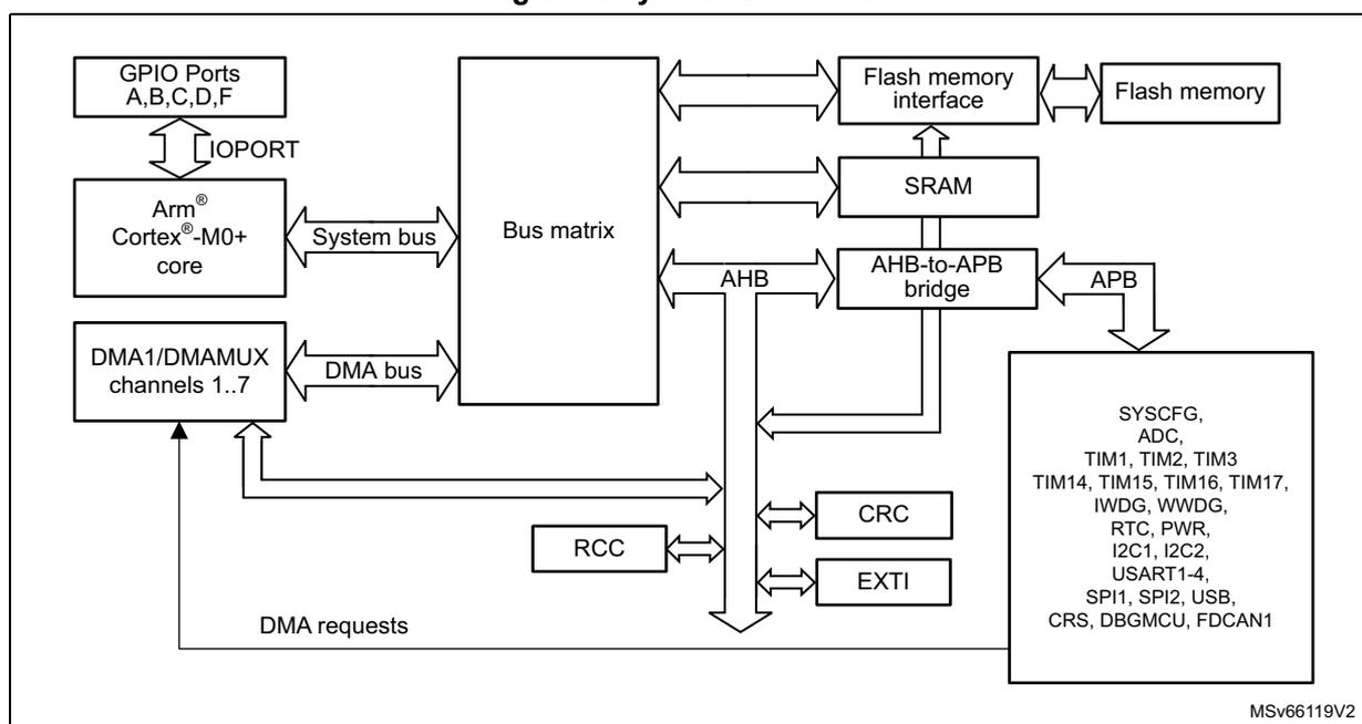
The diagram illustrates the system architecture. At the center is a 'Bus matrix'. To its left, the 'Arm ® Cortex ® -M0+ core' is connected via a 'System bus', and 'DMA1/DMAMUX channels 1..7' are connected via a 'DMA bus'. Above the core, 'GPIO Ports A,B,C,D,F' are connected via 'IOPORT'. Below the core, 'RCC' is connected to the DMA bus. The 'Bus matrix' is connected to 'Flash memory interface' (which connects to 'Flash memory'), 'SRAM', and 'AHB-to-APB bridge' via the 'AHB' bus. The 'AHB-to-APB bridge' connects to a large block of 'APB' peripherals, which includes SYSCFG, ADC, TIM1, TIM2, TIM3, TIM14, TIM15, TIM16, TIM17, IWDG, WWDG, RTC, PWR, I2C1, I2C2, USART1-4, SPI1, SPI2, USB, CRS, DBGMCU, and FDCAN1. 'CRC' and 'EXTI' are also connected to the AHB bus. 'DMA requests' are shown from the APB peripherals back to the DMA1/DMAMUX channels. A reference code 'MSV66119V2' is in the bottom right corner.
System bus (S-bus)
This bus connects the system bus of the Cortex ® -M0+ core (peripheral bus) to a bus matrix that manages the arbitration between the core and the DMA.
DMA bus
This bus connects the AHB master interface of the DMA to the bus matrix that manages the access of CPU and DMA to SRAM, flash memory and AHB/APB peripherals.
Bus matrix
The bus matrix arbitrates the access between the core system bus and the DMA master bus. The arbitration uses a Round Robin algorithm. The bus matrix is composed of masters (CPU, DMA) and slaves (flash memory interface, SRAM and AHB-to-APB bridge).
AHB peripherals are connected to the system bus through the bus matrix to allow DMA access.
AHB-to-APB bridge (APB)
The AHB-to-APB bridge provides full synchronous connections between the AHB and the APB bus.
Refer to Section 2.2: Memory organization for the address mapping of the peripherals connected to this bridge.
After each device reset, all peripheral clocks are disabled (except for the SRAM and flash memory). Before using a peripheral, its clock must first be enabled through the RCC_AHBENR, RCC_APBENRx, or RCC_IOPENR register.
Note: Unless otherwise specified, when a 16- or 8-bit access is performed on an APB register, the access is transformed into a 32-bit access: the bridge duplicates the 16- or 8-bit data to feed the 32-bit vector.
2.2 Memory organization
2.2.1 Introduction
Program memory, data memory, registers and I/O ports are organized within the same linear address space.
The bytes are coded in memory in Little Endian format. The lowest numbered byte in a word is considered the word's least significant byte and the highest numbered byte the most significant.
2.2.2 Memory map and register boundary addresses
Figure 2. Memory map
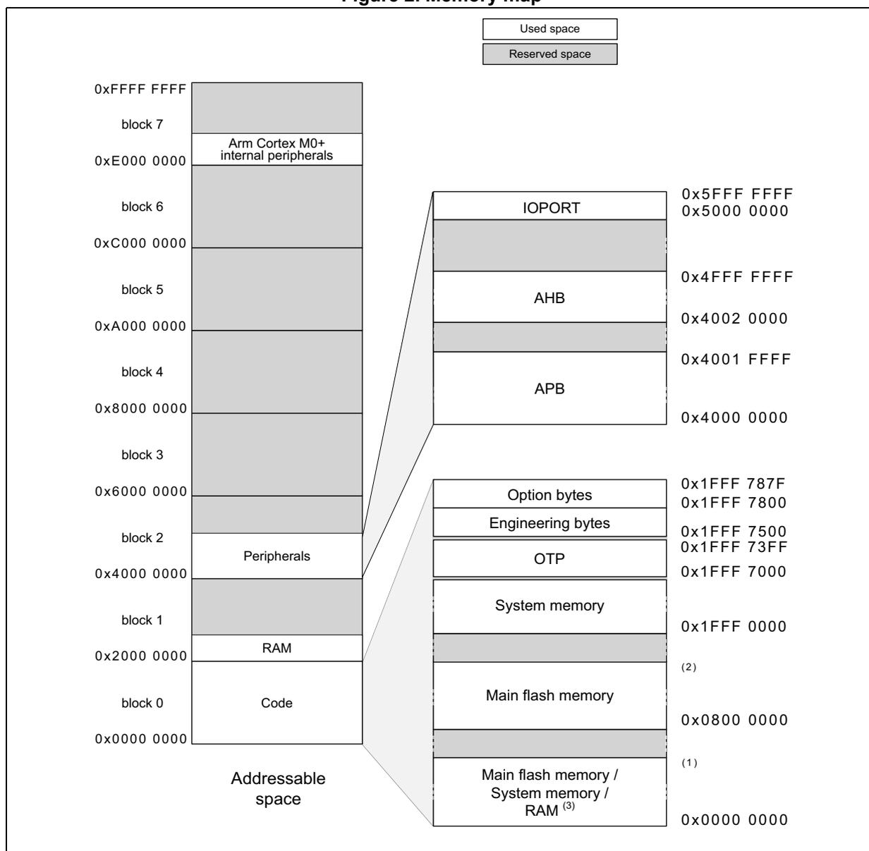
Legend:
- Used space (White)
- Reserved space (Grey)
Memory Map Details:
- Addressable space:
0x0000 0000 to 0xFFFF FFFF.
- Block 7: 0xE000 0000 to 0xFFFF FFFF (Arm Cortex M0+ internal peripherals)
- Block 6: 0xC000 0000 to 0xE000 0000 (Reserved space)
- Block 5: 0xA000 0000 to 0xC000 0000 (Reserved space)
- Block 4: 0x8000 0000 to 0xA000 0000 (Reserved space)
- Block 3: 0x6000 0000 to 0x8000 0000 (Reserved space)
- Block 2: 0x4000 0000 to 0x6000 0000 (Peripherals)
- Block 1: 0x2000 0000 to 0x4000 0000 (RAM)
- Block 0: 0x0000 0000 to 0x2000 0000 (Code)
- Used space (White):
- IOPORT: 0x5000 0000 to 0x5FFF FFFF
- AHB: 0x4002 0000 to 0x4FFF FFFF
- APB: 0x4000 0000 to 0x4001 FFFF
- Option bytes: 0x1FFF 787F to 0x1FFF 7800
- Engineering bytes: 0x1FFF 7500 to 0x1FFF 73FF
- OTP: 0x1FFF 7000 to 0x1FFF 7000
- System memory: 0x1FFF 0000 to 0x1FFF 0000
- Main flash memory: 0x0800 0000 to 0x1FFF 0000
- Main flash memory / System memory / RAM (3) : 0x0000 0000 to 0x0000 0000
- Reserved space (Grey):
- 0x0000 0000 to 0x0800 0000 (1)
- 0x1FFF 0000 to 0x1FFF 7000 (2)
- 0x4000 0000 to 0x5000 0000
- 0x5FFF 0000 to 0xFFFF FFFF
1. 0x0000 7FFF for STM32C011xx and STM32C031xx; 0x0800 FFFF for STM32C051xx; 0x0001 FFFF for STM32C071xx; 0x0003 FFFF for STM32C091xx/92xx
2. 0x0800 7FFF for STM32C011xx and STM32C031xx; 0x0000 FFFF for STM32C051xx; 0x0801 FFFF for STM32C071xx; 0x0803 FFFF for STM32C091xx/92xx
3. Depends on boot configuration
All the memory map areas that are not allocated to on-chip memories and peripherals are considered as reserved. For the detailed mapping of available memory and register areas, refer to the following tables.
Table 2. STM32C011xx and STM32C031xx boundary addresses| Type | Boundary address | Size | Memory Area | Register description |
|---|---|---|---|---|
| SRAM | 0x2000 3000 - 0x3FFF FFFF | ~512 MB | Reserved | - |
| 0x2000 0000 - 0x2000 2FFF | 12 KB | SRAM | - | |
| FLASH | 0x1FFF 7880- 0x1FFF FFFF | ~34 KB | Reserved | - |
| 0x1FFF 7800 - 0x1FFF 787F | 128 B | Option bytes | Section 4.4 on page 66 | |
| 0x1FFF 7500 - 0x1FFF 77FF | 768 B | Engineering bytes | - | |
| 0x1FFF 7400- 0x1FFF 74FF | 256 B | Reserved | - | |
| 0x1FFF 7000 - 0x1FFF 73FF | 1 KB | OTP | - | |
| 0x1FFF 1800- 0x1FFF 6FFF | ~22 KB | Reserved | - | |
| 0x1FFF 0000 - 0x1FFF 17FF | 6 KB | System memory | - | |
| 0x0800 8000 - 0x1FFE FFFF | ~384 MB | Reserved | - | |
| 0x0800 0000 - 0x0800 7FFF | 32 KB | Main flash memory | Section 4.3.1 on page 56 | |
| FLASH or SRAM | 0x0000 8000 - 0x07FF FFFF | ~127 MB | Reserved | - |
| 0x0000 0000 - 0x000 7FFF | 32 KB | Main flash memory, system memory, or SRAM, depending on boot configuration | - |
| Type | Boundary address | Size | Memory Area | Register description |
|---|---|---|---|---|
| SRAM | 0x2000 3000 - 0x3FFF FFFF | ~512 MB | Reserved | - |
| 0x2000 0000 - 0x2000 2FFF | 12 KB | SRAM | - | |
| FLASH | 0x1FFF 8000- 0x1FFF FFFF | 32 KB | Reserved | - |
| 0x1FFF 7800 - 0x1FFF 7FFF | 2 KB | Option bytes | Section 4.4 on page 66 | |
| 0x1FFF 7500 - 0x1FFF 77FF | 768 B | Engineering bytes | - | |
| 0x1FFF 7400- 0x1FFF 74FF | 256 B | Reserved | - | |
| 0x1FFF 7000 - 0x1FFF 73FF | 1 KB | OTP | - | |
| 0x1FFF 3000 - 0x1FFF 6FFF | 16 KB | Reserved | - | |
| 0x1FFF 0000 - 0x1FFF 2FFF | 12 KB | System memory | - | |
| 0x0801 0000 - 0x1FFE FFFF | ~384 MB | Reserved | - | |
| 0x0800 0000 - 0x0800 FFFF | 64 KB | Main flash memory | Section 4.3.1 on page 56 | |
| FLASH or SRAM | 0x0000 8000 - 0x07FF FFFF | ~127 MB | Reserved | - |
| 0x0000 0000 - 0x000 FFFF | 64 KB | Main flash memory, system memory, or SRAM, depending on boot configuration | - |
Table 4. STM32C071xx boundary addresses
| Type | Boundary address | Size | Memory Area | Register description |
|---|---|---|---|---|
| SRAM | 0x2000 6000 - 0x3FFF FFFF | ~512 MB | Reserved | - |
| 0x2000 0000 - 0x2000 5FFF | 24 KB | SRAM | - | |
| FLASH | 0x1FFF 8000- 0x1FFF FFFF | 32 KB | Reserved | - |
| 0x1FFF 7800 - 0x1FFF 7FFF | 2 KB | Option bytes | Section 4.4 on page 66 | |
| 0x1FFF 7500 - 0x1FFF 77FF | 768 B | Engineering bytes | - | |
| 0x1FFF 7400 - 0x1FFF 74FF | 256 B | Reserved | - | |
| 0x1FFF 7000 - 0x1FFF 73FF | 1 KB | OTP | - | |
| 0x1FFF 0000 - 0x1FFF 6FFF | 28 KB | System memory | - | |
| 0x0802 0000 - 0x1FFE FFFF | ~384 MB | Reserved | - | |
| 0x0800 0000 - 0x0801 FFFF | 128 KB | Main flash memory | Section 4.3.1 on page 56 | |
| FLASH or SRAM | 0x0002 0000 - 0x07FF FFFF | ~128 MB | Reserved | - |
| 0x0000 0000 - 0x0001 FFFF | 128 KB | Main flash memory, system memory, or SRAM, depending on boot configuration | - |
Table 5. STM32C091xx boundary addresses
| Type | Boundary address | Size | Memory Area | Register description |
|---|---|---|---|---|
| SRAM | 0x2000 9000 - 0x3FFF FFFF | ~512 MB | Reserved | - |
| 0x2000 0000 - 0x2000 8FFF | 36 KB | SRAM | - | |
| FLASH | 0x1FFF 8000- 0x1FFF FFFF | 32 KB | Reserved | - |
| 0x1FFF 7800 - 0x1FFF 7FFF | 2 KB | Option bytes | Section 4.4 on page 66 | |
| 0x1FFF 7500 - 0x1FFF 77FF | 768 B | Engineering bytes | - | |
| 0x1FFF 7400- 0x1FFF 74FF | 256 B | Reserved | - | |
| 0x1FFF 7000 - 0x1FFF 73FF | 1 KB | OTP | - | |
| 0x1FFF 4000 - 0x1FFF 6FFF | 12 KB | Reserved | - | |
| 0x1FFF 0000 - 0x1FFF 3FFF | 16 KB | System memory | - | |
| 0x0804 0000 - 0x1FFE FFFF | ~384 MB | Reserved | - | |
| 0x0800 0000 - 0x0803 FFFF | 256 KB | Main flash memory | Section 4.3.1 on page 56 | |
| FLASH or SRAM | 0x0004 0000 - 0x07FF FFFF | ~128 MB | Reserved | - |
| 0x0000 0000 - 0x0003 FFFF | 256 KB | Main flash memory, system memory, or SRAM, depending on boot configuration | - |
Table 6. STM32C092xx boundary addresses
| Type | Boundary address | Size | Memory Area | Register description |
|---|---|---|---|---|
| SRAM | 0x2000 7800 - 0x3FFF FFFF | ~512 MB | Reserved | - |
| 0x2000 0000 - 0x2000 77FF | 30 KB | SRAM | - | |
| FLASH | 0x1FFF 8000- 0x1FFF FFFF | 32 KB | Reserved | - |
| 0x1FFF 7800 - 0x1FFF 7FFF | 2 KB | Option bytes | Section 4.4 on page 66 | |
| 0x1FFF 7500 - 0x1FFF 77FF | 768 B | Engineering bytes | - | |
| 0x1FFF 7400- 0x1FFF 74FF | 256 B | Reserved | - | |
| 0x1FFF 7000 - 0x1FFF 73FF | 1 KB | OTP | - | |
| 0x1FFF 4000 - 0x1FFF 6FFF | 12 KB | Reserved | - | |
| 0x1FFF 0000 - 0x1FFF 3FFF | 16 KB | System memory | - | |
| 0x0804 0000 - 0x1FFE FFFF | ~384 MB | Reserved | - | |
| 0x0800 0000 - 0x0803 FFFF | 256 KB | Main flash memory | Section 4.3.1 on page 56 | |
| FLASH or SRAM | 0x0004 0000 - 0x07FF FFFF | ~128 MB | Reserved | - |
| 0x0000 0000 - 0x0003 FFFF | 256 KB | Main flash memory, system memory, or SRAM, depending on boot configuration | - |
Table 7. STM32C0 series peripheral register boundary addresses
| Bus | Boundary address | Size | Peripheral | Peripheral register map |
|---|---|---|---|---|
| - | 0xE000 0000 - 0xE00F FFFF | 1MB | Cortex ® -M0+ internal peripherals | - |
| IOPORT | 0x5000 1800 - 0x5FFF 17FF | ~256 MB | Reserved | - |
| 0x5000 1400 - 0x5000 17FF | 1 KB | GPIOF | Section 8.5.12 on page 194 | |
| 0x5000 1000 - 0x5000 13FF | 1 KB | Reserved | - | |
| 0x5000 0C00 - 0x5000 0FFF | 1 KB | GPIOE | Section 8.5.12 on page 194 | |
| 0x5000 0800 - 0x5000 0BFF | 1 KB | GPIOC | Section 8.5.12 on page 194 | |
| 0x5000 0400 - 0x5000 07FF | 1 KB | GPIOB | Section 8.5.12 on page 194 | |
| 0x5000 0000 - 0x5000 03FF | 1 KB | GPIOA | Section 8.5.12 on page 194 |
Table 7. STM32C0 series peripheral register boundary addresses (continued)
| Bus | Boundary address | Size | Peripheral | Peripheral register map |
|---|---|---|---|---|
| AHB | 0x4002 3400 - 0x4FFF FFFF | ~256 MB | Reserved | - |
| 0x4002 3000 - 0x4002 33FF | 1 KB | CRC | Section 15.4.6 on page 284 | |
| 0x4002 2400 - 0x4002 2FFF | 3 KB | Reserved | - | |
| 0x4002 2000 - 0x4002 23FF | 1 KB | FLASH | Section 4.7.14 on page 90 | |
| 0x4002 1C00 - 0x4002 1FFF | 3 KB | Reserved | - | |
| 0x4002 1800 - 0x4002 1BFF | 1 KB | EXTI | Section 14.5.16 on page 276 | |
| 0x4002 1400 - 0x4002 17FF | 1 KB | Reserved | - | |
| 0x4002 1000 - 0x4002 13FF | 1 KB | RCC | Section 6.4.24 on page 163 | |
| 0x4002 0C00 - 0x4002 0FFF | 1 KB | Reserved | - | |
| 0x4002 0800 - 0x4002 0BFF | 1 KB | DMAMUX | Section 12.6.7 on page 256 | |
| 0x4002 0400 - 0x4002 07FF | 1 KB | Reserved | - | |
| 0x4002 0000 - 0x4002 03FF | 1 KB | DMA1 | Section 11.6.7 on page 239 | |
| APB | 0x4001 5C00 - 0x4001 FFFF | 32 KB | Reserved | - |
| 0x4001 5800 - 0x4001 5BFF | 1 KB | DBG | Section 30.10.5 on page 1014 | |
| 0x4001 4C00 - 0x4001 57FF | 3 KB | Reserved | - | |
| 0x4001 4800 - 0x4001 4BFF | 1 KB | TIM17 | Section 20.6.21 on page 628 | |
| 0x4001 4400 - 0x4001 47FF | 1 KB | TIM16 | Section 20.6.21 on page 628 | |
| 0x4001 4000 - 0x4001 43FF | 1 KB | TIM15 | Section 20.6.21 on page 628 | |
| 0x4001 3C00 - 0x4001 3FFF | 1 KB | Reserved | - | |
| 0x4001 3800 - 0x4001 3BFF | 1 KB | USART1 | Section 26.8.15 on page 827 | |
| 0x4001 3400 - 0x4001 37FF | 1 KB | Reserved | - | |
| 0x4001 3000 - 0x4001 33FF | 1 KB | SPI1 | Section 27.9.10 on page 886 | |
| 0x4001 2C00 - 0x4001 2FFF | 1 KB | TIM1 | Section 17.4.29 on page 440 | |
| 0x4001 2800 - 0x4001 2BFF | 1 KB | Reserved | - | |
| 0x4001 2400 - 0x4001 27FF | 1 KB | ADC | Section 16.13 on page 342 | |
| 0x4001 0400 - 0x4001 23FF | 8 KB | Reserved | - | |
| 0x4001 0080 - 0x4001 03FF | 1 KB | SYSCFG(ITLINE) (1) | Section 9.1.34 on page 213 | |
| 0x4001 001D - 0x4001 007F | Reserved | - | ||
| 0x4001 0000 - 0x4001 001C | SYSCFG | Section 9.1.34 on page 213 | ||
| 0x4000 CC00 - 0x4000 FFFF | 19 KB | Reserved | - | |
| 0x4000 B800 - 0x4000 CBFF | 5 KB | FDCAN scratch RAM | - | |
| 0x4000 B400 - 0x4000 B7FF | 1 KB | FDCAN message RAM | - | |
| 0x4000 A000 - 0x4000 B3FF | 5 KB | Reserved | - | |
| 0x4000 9800 - 0x4000 9FFF | 2 KB | USB RAM | - | |
| 0x4000 8800 - 0x4000 97FF | 4 KB | Reserved | - | |
| 0x4000 7400 - 0x4000 87FF | 5 KB | Reserved | - | |
| 0x4000 7000 - 0x4000 73FF | 1 KB | PWR | Section 5.4.19 on page 115 | |
| 0x4000 6C00 - 0x4000 6FFF | 1 KB | CRS | Section 7.7.5 on page 176 |
| Bus | Boundary address | Size | Peripheral | Peripheral register map |
|---|---|---|---|---|
| APB | 0x4000 6800 - 0x4000 6BFF | 1 KB | Reserved | - |
| 0x4000 6400 - 0x4000 67FF | 1 KB | FDCAN1 | Section 28.4.38 on page 949 | |
| 0x4000 6000 - 0x4000 63FF | 1 KB | Reserved | - | |
| 0x4000 5C00 - 0x4000 5FFF | 1 KB | USB | Section 29.6.8 on page 994 | |
| 0x4000 5800 - 0x4000 5BFF | 1 KB | I2C2 | Section 25.9.12 on page 741 | |
| 0x4000 5400 - 0x4000 57FF | 1 KB | I2C1 | Section 25.9.12 on page 741 | |
| 0x4000 5000 - 0x4000 53FF | 1 KB | Reserved | - | |
| 0x4000 4C00 - 0x4000 4FFF | 1 KB | USART4 | Section 26.8.15 on page 827 | |
| 0x4000 4800 - 0x4000 4BFF | 1 KB | USART3 | Section 26.8.15 on page 827 | |
| 0x4000 4400 - 0x4000 47FF | 1 KB | USART2 | Section 26.8.15 on page 827 | |
| 0x4000 4000 - 0x4000 43FF | 1 KB | Reserved | - | |
| 0x4000 3C00 - 0x4000 3FFF | 1 KB | Reserved | - | |
| 0x4000 3800 - 0x4000 3BFF | 1 KB | SPI2 | Section 27.9.10 on page 886 | |
| 0x4000 3400 - 0x4000 37FF | 1 KB | Reserved | - | |
| 0x4000 3000 - 0x4000 33FF | 1 KB | IWDG | Section 22.4.6 on page 639 | |
| 0x4000 2C00 - 0x4000 2FFF | 1 KB | WWDG | Section 23.5.4 on page 645 | |
| 0x4000 2800 - 0x4000 2BFF | 1 KB | RTC | Section 24.6.18 on page 675 | |
| 0x4000 2400 - 0x4000 27FF | 1 KB | Reserved | - | |
| 0x4000 2000 - 0x4000 23FF | 1 KB | TIM14 | Section 19.4.13 on page 541 | |
| 0x4000 1800 - 0x4000 1FFF | 2 KB | Reserved | - | |
| 0x4000 1400 - 0x4000 17FF | 1 KB | Reserved | - | |
| 0x4000 1000 - 0x4000 13FF | 1 KB | Reserved | - | |
| 0x4000 0C00 - 0x4000 0FFF | 1 KB | Reserved | - | |
| 0x4000 0800 - 0x4000 0BFF | 1 KB | Reserved | - | |
| 0x4000 0400 - 0x4000 07FF | 1 KB | TIM3 | Section 18.4.26 on page 514 | |
| 0x4000 0000 - 0x4000 03FF | 1 KB | TIM2 | Section 18.4.26 on page 514 |
1. SYSCFG (ITLINE) registers use 0x4001 0000 as reference peripheral base address.
2.3 Embedded SRAM
The following table summarizes the SRAM resources on the devices, with parity check enabled and disabled.
Table 8. SRAM size| Device | SRAM with parity (Kbyte) |
|---|---|
| STM32C011xx | 6 |
| STM32C031xx, STM32C051xx | 12 |
| STM32C071xx | 24 |
Table 8. SRAM size (continued)
| Device | SRAM with parity (Kbyte) |
|---|---|
| STM32C092xx | 30 |
| STM32C091xx | 36 |
The SRAM can be accessed by bytes, half-words (16 bits) or full words (32 bits), at maximum system clock frequency without wait state and thus by both CPU and DMA.
Parity check
The user can enable the parity check using the option bit RAM_PARITY_CHECK in the user option byte (refer to Section 4.4: FLASH option bytes ).
The data bus width is 36 bits because 4 bits are available for parity check (1 bit per byte) in order to increase memory robustness, as required for instance by Class B or SIL norms.
The parity bits are computed and stored when writing into the SRAM. Then, they are automatically checked when reading. If one bit fails, an NMI is generated.
Note: When enabling the SRAM parity check, it is advised to initialize by software the whole SRAM at the beginning of the code, to avoid getting parity errors when reading non-initialized locations.
2.4 FDCAN RAM
FDCAN RAM is only present on the STM32C092xx devices.
The FDCAN peripheral uses the first 1 KB of FDCAN RAM as a message RAM. The next 5 KB (FDCAN scratch RAM) can be accessed by the user. As the memory is accessible only from APB bus, it can only be accessed by words. See section AHB-to-APB bridge (APB) .
Note: Before accessing the FDCAN RAM, enable the FDCAN1 clock.
2.5 Flash memory overview
The flash memory is composed of two distinct physical areas:
- • The main flash memory block. It contains the application program and user data if necessary.
- • The information block. It is composed of three parts:
- – Option bytes for hardware and memory protection user configuration.
- – System memory which contains the proprietary boot loader code.
- – OTP (one-time programmable) area
The flash memory interface implements instruction access and data access based on the AHB protocol. It implements the prefetch buffer that speeds up CPU code execution. It also implements the logic necessary to carry out the flash memory operations (Program/Erase) controlled through the flash memory registers.