47. Tamper and backup registers (TAMP)
47.1 Introduction
The antitamper detection circuit is used to protect sensitive data from external attacks. 32 32-bit backup registers are retained in all low-power modes and also in \( V_{BAT} \) mode. The backup registers, as well as other secrets in the device, are protected by this antitamper detection circuit with five tamper pins and nine internal tampers. The external tamper pins can be configured for edge detection, or level detection with or without filtering.
47.2 TAMP main features
- • A tamper detection can optionally erase the backup registers, SRAM2, cache, and cryptographic peripherals. The device resources protected by a tamper are named "device secrets". The list of device secrets is configurable by software.
- • 32×32-bit backup registers:
- – The backup registers (TAMP_BKPxR) are implemented in the backup domain that remains powered-on by \( V_{BAT} \) when the \( V_{DD} \) power is switched off.
- • Five tamper pin for five external tamper detection event:
- – Passive tampers: ultralow power edge or level detection with internal pull-up hardware management.
- – Configurable digital filter.
- • Nine internal tamper events to protect against transient or environmental perturbation attacks.
- • Each tamper can be configured in two modes:
- – Confirmed mode: immediate erase of secrets on tamper detection, including backup registers erase.
- – Potential mode: most of the secrets erase following a tamper detection are launched by software.
- • Any tamper detection can generate an RTC timestamp event.
- • TrustZone support:
- – Tamper secure or nonsecure configuration.
- – Backup registers configuration in three configurable-size areas:
- 1 read/write secure area
- 1 write secure/read nonsecure area
- 1 read/write nonsecure area.
- • Boot hardware key for secure AES, stored in backup registers, protected against read and write access.
- • Tamper configuration and backup registers privilege protection
- • Monotonic counter
47.3 TAMP functional description
47.3.1 TAMP block diagram
Figure 636. TAMP block diagram
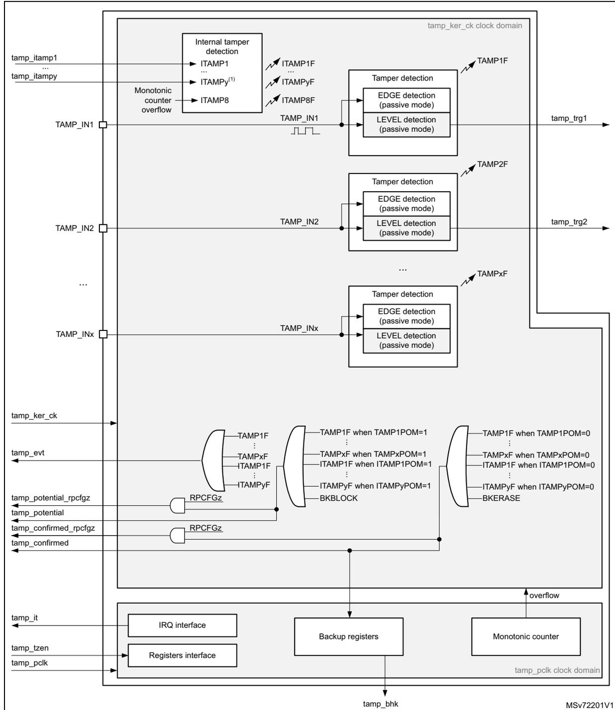
- 1. The number of external and internal tampers depends on products.
47.3.2 TAMP pins and internal signals
Table 491. TAMP input/output pins
| Pin name | Pin type | Description |
|---|---|---|
| TAMP_INx (x = pin index) | Input | Tamper input pin |
Table 492. TAMP internal input/output signals
| Internal signal name | Signal type | Description |
|---|---|---|
| tamp_ker_ck | Input | TAMP kernel clock, connected to rtc_ker_ck and also named RTCCLK in this document |
| tamp_pclk | Input | TAMP APB clock, connected to rtc_pclk |
| tamp_itamp[y] (y = signal index) | Inputs | Internal tamper event sources |
| tamp_tzen | Input | TAMP TrustZone enabled |
| tamp_evt | Output | Tamper event detection flag (internal or external tamper), whatever confirmed or potential mode configuration. |
| tamp_potential | Output | Potential tamper detection signal, used for device secrets protection
(1)
. This signal is active when: a tamper event detection flag (internal or external tamper), is generated in potential mode. or a software request is done by writing BKBLOCK to 1 |
| tamp_confirmed | Output | Confirmed tamper detection signal, used for device secrets
(1)
protection. This signal is active when: a tamper event detection flag (internal or external tamper), is generated in confirmed mode. or a software request is done by writing BKERASE to 1 |
| tamp_potential_rpcfgz (z = signal index) | Output | Potential tamper detection signal generated only when RPCFGz = 1. This signal is active when: a tamper event detection flag (internal or external tamper), is generated in potential mode. or a software request is done by writing BKBLOCK to 1 |
| tamp_confirmed_rpcfgz (z = signal index) | Output | Confirmed tamper detection signal generated only when RPCFGz = 1. This signal is active when: a tamper event detection flag (internal or external tamper), is generated in confirmed mode. or a software request is done by writing BKERASE to 1 |
| tamp_it | Output | TAMP interrupt (refer to Section 47.5: TAMP interrupts for details) |
| tamp_trg[x] (x = signal index) | Output | Tamper detection trigger |
| tamp_bhk | Output | Tamper boot hardware key bus |
1. Refer to Table 493: TAMP interconnection .
The TAMP kernel clock is usually the LSE at 32.768 kHz although it is possible to select other clock sources in the RCC (refer to RCC for more details). The TAMP kernel clock is required only for external tamper inputs level with filtering, and for external active tamper detection modes. Internal tampers detection and external tampers inputs edge detection are functional without requiring any kernel clock.
Read and write access to backup registers and all other TAMP registers are also functional without any kernel clock (only APB clock is needed).
Some detections modes are not available in some low-power modes or \( V_{BAT} \) depending on the selected clock (refer to Section 47.4: TAMP in low-power modes for more details).
Table 493. TAMP interconnection
| Signal name | Source/Destination |
|---|---|
| tamp_tzen | From FLASH option bytes: TZEN |
| tamp_evt | rtc_tamp_evt used to generate a timestamp event |
| tamp_potential | No effect |
| tamp_confirmed | No effect |
| tamp_potential_rpcfg1 | When the bit RPCFG1 is set in the TAMP_RPCFGGR, the tamp_potential_rpcfg1 signal is used to block the read and write accesses to the device secrets listed hereafter: – SRAM2 |
| tamp_confirmed_rpcfg1 | When the bit RPCFG1 is set in the TAMP_RPCFGGR, the tamp_confirmed_rpcfg1 signal is used to erase the device secrets listed hereafter: – SRAM2 The device secrets access is blocked when erase is ongoing. |
| tamp_potential_rpcfg2 | When the bit RPCFG2 is set in the TAMP_RPCFGGR, the tamp_potential_rpcfg2 signal is used to block the device secrets listed hereafter: – RHUK and to erase the device secrets listed hereafter: – SAES, AES, CCB |
| tamp_confirmed_rpcfg2 | When the bit RPCFG2 is set in the TAMP_RPCFGGR, the tamp_confirmed_rpcfg2 signal is used to block the device secrets listed hereafter: – RHUK and to erase the device secrets listed hereafter: – SAES, AES, CCB |
| tamp_potential_rpcfg3 | When the bit RPCFG3 is set in the TAMP_RPCFGGR, the tamp_potential_rpcfg3 signal is used to erase the device secrets listed hereafter: – ICACHE The device secrets access is blocked when erase is ongoing. |
| tamp_confirmed_rpcfg3 | When the bit RPCFG3 is set in the TAMP_RPCFGGR, the tamp_confirmed_rpcfg3 signal is used to erase the device secrets listed hereafter: – ICACHE The device secrets access is blocked when erase is ongoing. |
| tamp_potential_rpcfg4 | When the bit RPCFG4 is set in the TAMP_RPCFGGR, the tamp_potential_rpcfg4 signal is used to erase the device secrets listed hereafter: – HASH |
Table 493. TAMP interconnection (continued)
| Signal name | Source/Destination |
|---|---|
| tamp_confirmed_rpcfg4 | When the bit RPCFG4 is set in the TAMP_RPCFGGR, the tamp_confirmed_rpcfg4 signal is used to erase the device secrets listed hereafter: – HASH |
| tamp_potential_rpcfg5 | When the bit RPCFG5 is set in the TAMP_RPCFGGR, the tamp_potential_rpcfg5 signal is used to erase the device secrets listed hereafter: – PKA including PKA SRAM The device secrets access is blocked when erase is ongoing. |
| tamp_confirmed_rpcfg5 | When the bit RPCFG5 is set in the TAMP_RPCFGGR, the tamp_confirmed_rpcfg5 signal is used to erase the device secrets listed hereafter: – PKA including PKA SRAM The device secrets access is blocked when erase is ongoing. |
| tamp_itamp3 | LSE monitoring (LSECSS) (1) |
| tamp_itamp5 | RTC calendar overflow (rtc_calovf) |
| tamp_itamp6 | JTAG/SWD access when RDP > 0 |
| tamp_itamp7 | ADC1 (adc1_awd1) analog watchdog monitoring 1 |
| tamp_itamp8 (2) | Monotonic counter 1 overflow |
| tamp_itamp9 | Cryptographic peripherals fault (SAES or AES or PKA or TRNG or CCB) |
| tamp_itamp11 | IWDG reset when tamper flag is set (potential tamper timeout) |
| tamp_itamp12 | ADC1 (adc1_awd2) analog watchdog monitoring 2 |
| tamp_itamp13 | ADC1 (adc1_awd3) analog watchdog monitoring 3 |
| tamp_bhk | saes_bhk. This bus is used to load the boot hardware key in the secure AES co-processor. |
1. This monitoring must be enabled by setting LSECSSON in RCC backup domain control register (RCC_BDCR) .
2. This signal is generated in the TAMP peripheral.
The TZEN option bit is used to activate TrustZone in the device.
- • TZEN = 1: TrustZone activated.
- • TZEN = 0: TrustZone disabled.
When TrustZone is disabled, the APB accesses to the TAMP registers are nonsecure.
47.3.3 GPIOs controlled by the RTC and TAMP
The GPIOs with TAMP functions available in Standby mode are directly controlled by the TAMP, whatever the GPIO configuration.
The TAMP_INy function is enabled on a GPIO when TAMPyE = 1.
The GPIOs included in the battery backup domain ( \( V_{BAT} \) ) are directly controlled by the peripherals providing functions on these I/Os, whatever the GPIO configuration.
RTC_OUT1, RTC_TS and TAMP_IN1 are mapped on the same pin (PC13). The RTC and TAMP functions mapped on PC13 are available in all low-power modes and in \( V_{BAT} \) mode.
Table 494. PC13 pin configuration (1)| Pin function | OSEL[1:0] (ALARM output enable) | TAMPOE (TAMPER output enable) | COE (CALIB output enable) | TAMPALRM_TYPE | TAMPALRM_PU | TAMP1E (TAMP_IN1 input enable) | TSE (RTC_TS input enable) | |
|---|---|---|---|---|---|---|---|---|
| TAMPALRM output Push-Pull | 01 or 10 or 11 | 0 | Don't care | 0 | 0 | Don't care | Don't care | |
| 00 | 1 | |||||||
| 01 or 10 or 11 | 1 | |||||||
| TAMPALRM (2) Open-Drain | No pull | 01 or 10 or 11 | 0 | Don't care | 1 | 0 | Don't care | Don't care |
| 00 | 1 | |||||||
| 01 or 10 or 11 | 1 | |||||||
| Internal pull-up | 01 or 10 or 11 | 0 | 1 | |||||
| 00 | 1 | |||||||
| 01 or 10 or 11 | 1 | |||||||
| CALIB output PP | 00 | 0 | 1 | Don't care | Don't care | Don't care | Don't care | |
| TAMP_IN1 input floating | 00 | 0 | 0 | Don't care | Don't care | 1 | 0 | |
| 00 | 0 | 1 | ||||||
| Don't care | Don't care | 0 | ||||||
| RTC_TS and TAMP_IN1 input floating | 00 | 0 | 0 | Don't care | Don't care | 1 | 1 | |
| 00 | 0 | 1 | ||||||
| Don't care | Don't care | 0 | ||||||
| RTC_TS input floating | 00 | 0 | 0 | Don't care | Don't care | 0 | 1 | |
| 00 | 0 | 1 | ||||||
| Don't care | Don't care | 0 | ||||||
| Wake-up pin or Standard GPIO | 00 | 0 | 0 | Don't care | Don't care | 0 | 0 | |
| 00 | 0 | 1 | ||||||
| Don't care | Don't care | 0 | ||||||
1. OD: open drain; PP: push-pull.
2. In this configuration the GPIO must be configured in input.
47.3.4 TAMP register write protection
After system reset, the TAMP registers (including backup registers) are protected against parasitic write access by the DBP bit in the power control peripheral (refer to the PWR power control section). DBP bit must be set in order to enable TAMP registers write access.
47.3.5 TAMP secure protection modes
By default after a backup domain power-on reset, all TAMP registers can be read or written in both secure and nonsecure modes, except for the TAMP secure configuration register (TAMP_SECCFGR) which can be written in secure mode only. The TAMP protection configuration is not affected by a system reset.
- • When the TAMPSEC bit is set in the TAMP_SECCFGR register:
- – Writing the TAMP registers is possible only in secure mode, except for the backup registers and monotonic counter which have their own protection setting.
- – Reading TAMP_SECCFGR, TAMP_PRIVCFGR and TAMP_MISR is always possible in secure and nonsecure modes. All the other TAMP registers can be read only in secure mode, except for the backup registers and monotonic counter which have their own protection setting.
- • When the CNT1SEC bit is set in the TAMP_SECCFGR register, the TAMP_COUNT1R can be read and written only in secure mode, and CNT1PRIV can be written only in secure mode.
- • When the BKPRWSEC bit is set in the TAMP_SECCFGR register, the BKPRWPRIV bit can be written only in secure mode.
- • When the BKPWSEC bit is set in the TAMP_SECCFGR register, the BKPRWPRIV and BKPWPRIV bits can be written only in secure mode.
A nonsecure access to a secure-protected register is denied:
- • There is no bus error generated.
- • A notification is generated through a flag/interrupt in the IAC (illegal access controller).
- • When write protected, the bits are not written.
- • When read protected they are read as 0.
As soon as at least one function is configured to be secured, the TAMP reset and clock control is also secured in the RCC.
47.3.6 Backup registers protection zones
The backup registers protection is configured thanks to BKPRWSEC[7:0] and BKPWSEC[7:0] (refer to the figure below):
Figure 637. Backup registers protection zones
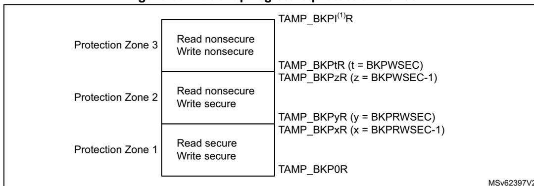
| Protection Zone 3 | Read nonsecure Write nonsecure | TAMP_BKPI (1) R |
| Read nonsecure Write secure | TAMP_BKPI
l
(t = BKPWSEC) TAMP_BKPI z (z = BKPWSEC-1) | |
| TAMP_BKPyR (y = BKPRWSEC) TAMP_BKPxR (x = BKPRWSEC-1) | ||
| Protection Zone 2 | Read secure Write secure | TAMP_BKP0R |
MSv62397V2
1. l = last backup register index
47.3.7 TAMP privilege protection modes
By default after a backup domain power-on reset, all TAMP registers can be read or written in both privileged and nonprivileged modes, except for the TAMP privilege configuration register (TAMP_PRIVCFGGR) which can be written in privilege mode only. The TAMP protection configuration is not affected by a system reset.
- • When the TAMPPRIV bit is set in the TAMP_PRIVCFGGR register:
- – Writing the TAMP registers is possible only in privilege mode, except for the backup registers and the monotonic counter, which have their own protection settings.
- – Reading the TAMP_SECCFGR and TAMP_PRIVCFGGR registers is always possible in both privilege and unprivileged modes. All other TAMP registers can be read only in privilege mode, except for the backup registers and the monotonic counter, which have their own protection settings.
- • When the CNT1PRIV bit is set in the TAMP_PRIVCFGGR register, the TAMP_COUNT1R register can be read and written only in privilege mode, and CNT1SEC can be written only in privilege mode.
- • When the BKPRWPRIV bit is set in the TAMP_PRIVCFGGR register, the BKPRWSEC register can be written only in privilege mode.
- • When the BKPWPRIV bit is set in the TAMP_PRIVCFGGR register, the BKPRWSEC and BKPWSEC registers can be written only in privilege mode.
The backup registers protection is configured thanks to BKPRWSEC[7:0] and BKPRWPRIV for the protection zone 1, and thanks to BKPRWSEC[7:0], BKPWSEC[7:0], and BKPWPRIV for the protection zone 2 (refer to Figure 637: Backup registers protection zones ). The BHKLOCK bit can be written only in privileged mode when the BKPRWPRIV bit is set.
A nonprivileged access to a privileged-protected register is denied:
- • There is no bus error generated.
- • When write protected, the bits are not written.
- • When read protected they are read as 0.
47.3.8 Boot hardware key (BHK)
The eight first backup registers from TAMP_BKP0R to TAMP_BKP7R can be used to store a boot hardware key for the secure AES.
For this purpose, these registers must belong to the protection zone 1: BKPRWSEC must be greater or equal to 8.
Once the backup registers are written with the boot hardware key, the BHKLOCK bit must be set in the TAMP_SECCFGR register. Once BHKLOCK is set, the eight backup registers cannot be accessed anymore by software: they are read as 0 and write to these registers is ignored. BHKLOCK cannot be cleared by software, and is cleared by hardware following a confirmed tamper event (if RPCFG31 = 1) or when the readout protection (RDP) is disabled. It is also cleared with BKERASE command if RPCFG31 = 1 (in all cases the backup registers are also erased).
Refer to section secure AES coprocessor (SAES) for details on the procedure to download the boot hardware key in the SAES.
47.3.9 Tamper detection
The tamper detection main purpose is to protect the device secrets from device external attacks. The detection is made on events on TAMP_INx (x = pin index) I/Os, or on internal monitors detecting out-of-range device conditions.
The tamper detection can be configured for the following purposes:
- • Erase the backup registers and other device secrets stored in SRAMs or peripherals listed in Table 493: TAMP interconnection . The device secrets list is configurable thanks to TAMP_RPCFGR.
- • Block the read/write access to the backup registers and other device secrets stored in SRAMs or peripherals listed in Table 493: TAMP interconnection . The device secrets list is configurable thanks to TAMP_RPCFGR.
- • Generate an interrupt, capable to wake up from low-power modes.
- • Generate a hardware trigger for the low-power timers, or an RTC timestamp event.
The external I/Os tamper detection supports passive mode: TAMP_INx I/Os are monitored and a tamper is detected either on edge or level.
A digital filter can be applied on external tamper detection to avoid false detection. In addition, it is possible to configure each tamper source in potential mode, so that the secrets erase is not launched by hardware on tamper detection. The secrets erase can then be launched by software after software checks.
47.3.10 TAMP backup registers and other device secrets erase
The backup registers (TAMP_BKPxR) are not reset by system reset or when the device wakes up from Standby mode.
The backup registers and the other device secrets are not reset when the corresponding mask is set
(TAMPxMSK = 1 in the TAMP_CR2 register).
Note: The backup registers are also erased when the readout protection of the flash is changed from level 1 to level 0.
47.3.11 Tamper detection - confirmed mode
The confirmed mode is selected for TAMPx (external tamper x) when TAMPxPOM = 0 in the TAMP_CR2 register. The confirmed mode is selected for ITAMPx (internal tamper x) when ITAMPxPOM = 0 in the TAMP_CR3 register. The effects of a tamper detection in confirmed
mode are described with
tamp_confirmed
and
tamp_confirmed_rpcfgx
signals in
Table 493: TAMP interconnection
.
This mode is selected to automatically erase the device secrets when the tamper is detected.
Tamper detection - potential mode
The potential mode is selected for TAMPx (external tamper x) when
TAMPxPOM = 1
in the
TAMP_CR2
register. The potential tamper mode is selected for ITAMPx (internal tamper x) when
ITAMPxPOM = 1
in the
TAMP_CR3
register. The effects of a tamper detection in potential mode are described with
tamp_potential
and
tamp_potential_rpcfgx
signals in
Table 493: TAMP interconnection
.
This mode is selected to avoid irreversible erasure of some device secrets when the tamper is detected. In this mode, some device secrets are not erased when the corresponding tamper event is detected. In addition, the read and write accesses to these device secrets are blocked as soon as the tamper detection flag is set in potential mode, until this flag is cleared by setting the corresponding clear flag in the
TAMP_SCR
register. Therefore the software can perform some checks to discriminate false from true tampers, and decide to launch secrets erase only in case of the potential tamper is confirmed to be a true tamper. The device secrets are erased by software by setting the
BKERASE
bit in the
TAMP_CR2
register.
Potential tamper to confirm tamper timeout
Some internal tampers generate a tamper event if the independent watchdog reset occurs when another tamper flag is set (refer to
Table 493: TAMP interconnection
). The IWDG tamper must be configured with
ITAMPxPOM = 0
. This permits the erasure of device secrets to be forced by hardware after a timeout, in case the previous tamper event was in potential mode. This is equivalent to change the "potential tamper" into "confirmed tamper" if a watchdog reset occurs before any software decision following the potential tamper event.
Device resources protection configuration
Some device resources can be configured in order to be included to the list of the device secrets protected by tamper detection.
When
RPCFGz = 0
in the
TAMP_RPCFGR
, the device resource associated to
RPCFGz
is not protected by the TAMP peripheral:
- • It is not affected by tamper detection (whatever confirmed or potential mode).
- • It is not affected by
BKERASEsoftware command. - • It is not affected by
BKBLOCKsoftware command.
When
RPCFGz = 1
in the
TAMP_RPCFGR
, the device resource associated to
RPCFGz
is protected by the TAMP peripheral:
- • It is affected by confirmed tamper detection and
BKERASEsoftware command, as described withtamp_confirmed_rpcfgzsignal in Table 493: TAMP interconnection . - • It is affected by potential tamper detection and
BKBLOCKsoftware command, as described withtamp_potential_rpcfgzsignal in Table 493: TAMP interconnection .
| - | Potential tamper or BKBLOCK | Confirmed tamper or BKERASE |
|---|---|---|
| RPCFG31 = 0 | No effect on backup registers, BHK and BHKLOCK | No effect on backup registers, BHK and BHKLOCK |
| RPCFG31 = 1 | Backup registers and BHK access is blocked | Backup registers, BHK and BHKLOCK are erased |
| - | Potential tamper or BKBLOCK | Confirmed tamper or BKERASE |
|---|---|---|
| RPCFGx = 0 | No effect on device resource x | No effect on device resource x |
| RPCFGx = 1 | Device secret x protected as described by
tamp_potential_rpcfgx
(1) | Device secret x protected as described by
tamp_confirmed_rpcfgx
(1) |
1. Refer to Table 493: TAMP interconnection .
Device secrets access blocked by software
By default, the device secrets can be accessed by the application, except if a tamper event flag is detected: the device secrets access is not possible as long as a tamper flag is set.
It is possible to block the access to the device secrets by software, by setting the BKBLOCK bit of the TAMP_CR2 register. The device secrets access is possible only when BKBLOCK = 0 and no tamper flag is set.
47.3.12 Tamper detection configuration and initialization
Each input can be enabled by setting the corresponding TAMPxE bits to 1 in the TAMP_CR register. Each TAMP_INx tamper detection input is associated with a flag TAMPxF in the TAMP_SR register.
By setting the TAMPxE bit in the TAMP_IER register, an interrupt is generated when a tamper detection event occurs (when TAMPxF is set). Setting TAMPxE is not allowed when the corresponding TAMPxMSK is set.
Trigger output generation on tamper event
The tamper event detection can be used as a trigger input by the low-power timers.
When TAMPxMSK bit is cleared in TAMP_CR register, the TAMPxF flag must be cleared by software in order to allow a new tamper detection on the same pin.
When TAMPxMSK bit is set, the TAMPxF flag is masked, and kept cleared in TAMP_SR register. This configuration permits the low-power timers to be triggered automatically in Stop mode, without requiring the system wake-up to perform the TAMPxF clearing. In this case, the backup registers are not cleared.
This feature is available only when the tamper is configured in level detection with filtering mode (
TAMPFLT ≠ 00
). Refer to
Level detection with filtering on tamper inputs (passive mode)
.
Timestamp on tamper event
With TAMPTS set to 1 in the RTC_CR, any internal or external tamper event causes a timestamp to occur. When TAMPTS is 0, any external tamper can be individually configured to cause or not a timestamp. A global configuration for all internal tampers is also available to enable or not timestamp on internal tamper detection (refer to RTC_TAMPTSCR). In case a timestamp occurs due to tamper event, either the TSF bit or the TSOVF bit is set in RTC_SR, in the same manner as if a normal timestamp event occurs. The TSID bitfield in the RTC_TSIDR provides the identification of the cause of the timestamp event.
Caution: Timestamp on tamper event must be disabled before entering RTC initialization mode (TAMPTS, and all bits of RTC_TAMPTSCR must be cleared before setting the INIT bit in RTC_ICSR).
Note: TSF is set up to three ck_apre cycles after TAMPxF flags. TSF is not set if RTCCLK is stopped (it is set when RTCCLK restarts).
If TAMPxF is cleared before the expected rise of TSF, TSF is not set. Consequently, in case TAMPTS = 1 or any bit in TAMP_TAMPTSCR register is set, the software either waits for the timestamp flag before clearing the tamper flag, or reads the RTC counters values in the TAMP interrupt routine.
Edge detection on tamper inputs (passive mode)
If the TAMPFLT bits are 00, the TAMP_INx pins generate tamper detection events when either a rising edge or a falling edge is observed depending on the corresponding TAMPxTRG bit. The internal pull-up resistors on the TAMP_INx inputs are deactivated when edge detection is selected.
Caution: When TAMPFLT = 00 and TAMPxTRG = 0 (rising edge detection), a tamper event may be detected by hardware if the tamper input is already at high level before enabling the tamper detection.
After a tamper event has been detected and cleared, the TAMP_INx should be disabled and then reenabled (TAMPxE set to 1) before reprogramming the backup registers (TAMP_BKPxR). This prevents the application from writing to the backup registers while the TAMP_INx input value still indicates a tamper detection. This is equivalent to a level detection on the TAMP_INx input.
Note: Tamper detection is still active when V DD power is switched off. To avoid unwanted resetting of the backup registers, the pin to which the TAMPx is mapped should be externally tied to the correct level.
Level detection with filtering on tamper inputs (passive mode)
Level detection with filtering is performed by setting TAMPFLT to a nonzero value. A tamper detection event is generated when either two, four, or eight (depending on TAMPFLT) consecutive samples are observed at the level designated by the TAMPxTRG bits.
The TAMP_INx inputs are precharged through the I/O internal pull-up resistance before its state is sampled, unless disabled by setting TAMPPUDIS to 1. The duration of the precharge is determined by the TAMPPRCH bits, allowing for larger capacitances on the TAMP_INx inputs.
The trade-off between tamper detection latency and power consumption through the pull-up can be optimized by using TAMPFREQ to determine the frequency of the sampling for level detection. The TAMP_IN I/O schmitt trigger is enabled only during the precharge duration to avoid any extra consumption if the tamper switch is open (floating state).
Figure 638. Tamper sampling with precharge pulse
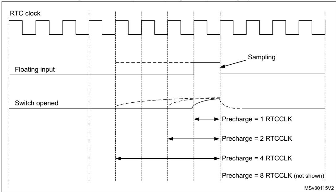
The diagram shows three signal lines over time. The top line is the 'RTC clock', a periodic square wave. The middle line is the 'Floating input', which is initially high and then drops to low when the 'Switch opened' (bottom line) occurs. Vertical dashed lines indicate sampling points. Arrows indicate precharge durations starting from the switch opening and ending at the next sampling point: 'Precharge = 1 RTCCLK', 'Precharge = 2 RTCCLK', 'Precharge = 4 RTCCLK', and 'Precharge = 8 RTCCLK (not shown)'. The label 'Sampling' points to a falling edge of the clock. The code 'MSv30115V2' is in the bottom right corner.
Figure 639. Low level detection with precharge and filtering
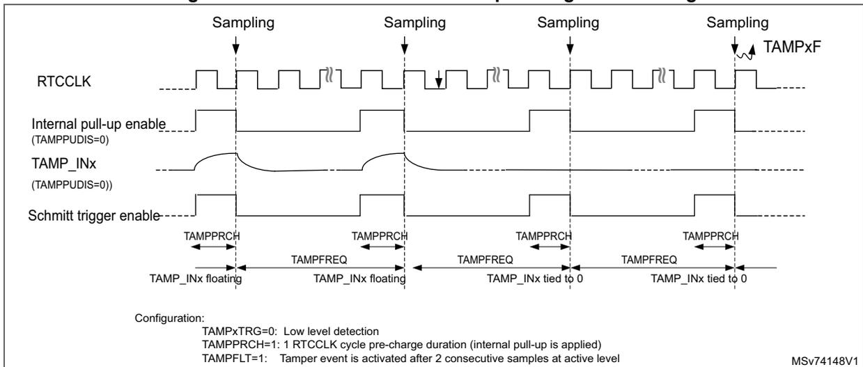
The diagram shows four signal lines over time. The top line is 'RTCCLK'. The second line is 'Internal pull-up enable (TAMPPUDIS=0)'. The third line is 'TAMP_INx (TAMPPUDIS=0)'. The bottom line is 'Schmitt trigger enable'. The diagram is divided into four sampling periods. In the first two, 'TAMP_INx' is 'floating'. In the third and fourth, it is 'tied to 0'. 'Sampling' points are marked with downward arrows. 'TAMPPRCH' (precharge duration) and 'TAMPFREQ' (tamper frequency) intervals are indicated. A configuration section at the bottom left specifies: 'TAMPxTRG=0: Low level detection', 'TAMPPRCH=1: 1 RTCCLK cycle pre-charge duration (internal pull-up is applied)', and 'TAMPFLT=1: Tamper event is activated after 2 consecutive samples at active level'. The code 'MSv74148V1' is in the bottom right corner.
Note: Refer to the microcontroller datasheet for the electrical characteristics of the pull-up resistors.
47.4 TAMP in low-power modes
Table 497. Effect of low-power modes on TAMP
| Mode | Description |
|---|---|
| Sleep | No effect. TAMP interrupts cause the device to exit the Sleep mode. |
| Stop | No effect on all features, except for level detection with filtering mode which remain active only when the clock source is LSE or LSI. Tamper interrupts cause the device to exit the Stop mode. |
| Standby | No effect on all features, except for level detection with filtering mode which remain active only when the clock source is LSE or LSI. Tamper interrupts cause the device to exit the Standby mode. |
| Shutdown | No effect on all features, except for level detection with filtering mode which remain active only when the clock source is LSE. Tamper interrupts cause the device to exit the Shutdown mode. |
Table 498. TAMP pins functionality over modes
| Pin name | Functional in all low-power modes | Functional in VBAT mode |
|---|---|---|
| TAMP_IN[5:1] | Yes | Yes |
47.5 TAMP interrupts
The interrupt channel is set in the masked interrupt status register or in the secure masked interrupt status register depending on its security mode configuration (TAMPSEC).
Table 499. Interrupt requests
| Interrupt acronym | Interrupt event | Event flag (1) | Enable control bit | Interrupt clear method | Exit from low-power modes |
|---|---|---|---|---|---|
| TAMP | Tamper x (2) | TAMPxF | TAMPxIE | Write 1 in CTAMPxF | Yes (3) |
| Internal tamper y (2) | ITAMPyF | ITAMPyIE | Write 1 in CITAMPyF | Yes (3) |
- 1. The event flags are in the TAMP_SR register.
- 2. The number of tampers and internal tampers events depend on products.
- 3. Refer to Section 47.4: TAMP in low-power modes for more details about available features in the low-power modes.
47.6 TAMP registers
47.6.1 TAMP control register 1 (TAMP_CR1)
Address offset: 0x000
Backup domain reset value: 0x0000 0000
System reset value: 0xUUUU UUUU
This register can be protected against nonsecure access (refer to Section 47.3.5: TAMP secure protection modes ). This register can be protected against unprivileged access (refer to Section 47.3.7: TAMP privilege protection modes ).
This register is not affected by System reset value.
| 31 | 30 | 29 | 28 | 27 | 26 | 25 | 24 | 23 | 22 | 21 | 20 | 19 | 18 | 17 | 16 |
|---|---|---|---|---|---|---|---|---|---|---|---|---|---|---|---|
| Res. | Res. | Res. | ITAMP1 3E | ITAMP1 2E | ITAMP1 1E | Res. | ITAMP9 E | ITAMP8 E | ITAMP7 E | ITAMP6 E | ITAMP5 E | Res. | ITAMP3 E | Res. | Res. |
| rw | rw | rw | rw | rw | rw | rw | rw | rw |
| 15 | 14 | 13 | 12 | 11 | 10 | 9 | 8 | 7 | 6 | 5 | 4 | 3 | 2 | 1 | 0 |
|---|---|---|---|---|---|---|---|---|---|---|---|---|---|---|---|
| Res. | Res. | Res. | Res. | Res. | Res. | Res. | Res. | Res. | Res. | Res. | TAMP5 E | TAMP4 E | TAMP3 E | TAMP2 E | TAMP1 E |
| rw | rw | rw | rw | rw |
Bits 31:29 Reserved, must be kept at reset value.
Bits 28:26 ITAMPiE : Internal tamper i enable (i = 13 to 11)
0: Internal tamper i disabled
1: Internal tamper i enabled
Bit 25 Reserved, must be kept at reset value.
Bits 24:20 ITAMPiE : Internal tamper i enable (i = 9 to 5)
0: Internal tamper i disabled
1: Internal tamper i enabled
Bit 19 Reserved, must be kept at reset value.
Bit 18 ITAMP3E : Internal tamper 3 enable
0: Internal tamper 3 disabled
1: Internal tamper 3 enabled
Bits 17:5 Reserved, must be kept at reset value.
Bits 4:0 TAMPiE : Tamper detection on TAMP_INi enable (i = 5 to 1)
0: Tamper detection on TAMP_INi disabled
1: Tamper detection on TAMP_INi enabled
Note: Tamper detection mode (selected with TAMP_FLTCR and TAMPxTRG bits in TAMP_CR2), must be configured before enabling the tamper detection.
47.6.2 TAMP control register 2 (TAMP_CR2)
Address offset: 0x004
Backup domain reset value: 0x0000 0000
System reset value: 0xUUUU UUUU
This register can be protected against nonsecure access (refer to Section 47.3.5: TAMP secure protection modes ). This register can be protected against unprivileged access (refer to Section 47.3.7: TAMP privilege protection modes ).
This register is not affected by System reset value.
| 31 | 30 | 29 | 28 | 27 | 26 | 25 | 24 | 23 | 22 | 21 | 20 | 19 | 18 | 17 | 16 |
|---|---|---|---|---|---|---|---|---|---|---|---|---|---|---|---|
| Res. | Res. | Res. | TAMP5 TRG | TAMP4 TRG | TAMP3 TRG | TAMP2 TRG | TAMP1 TRG | BKERA SE | BKBLO CK | Res. | Res. | Res. | TAMP3 MSK | TAMP2 MSK | TAMP1 MSK |
| rw | rw | rw | rw | rw | w | rw | rw | rw | rw |
| 15 | 14 | 13 | 12 | 11 | 10 | 9 | 8 | 7 | 6 | 5 | 4 | 3 | 2 | 1 | 0 |
|---|---|---|---|---|---|---|---|---|---|---|---|---|---|---|---|
| Res. | Res. | Res. | Res. | Res. | Res. | Res. | Res. | Res. | Res. | Res. | TAMP5 POM | TAMP4 POM | TAMP3 POM | TAMP2 POM | TAMP1 POM |
| rw | rw | rw | rw | rw |
Bits 31:29 Reserved, must be kept at reset value.
Bits 28:24 TAMPiTRG : Active level for tamper i input (i = 5 to 1)
If TAMPFLT[1:0] = 00 in TAMP_FLTCR, the tamper i input rising edge triggers a tamper detection event, and the tamper i input falling edge triggers a tamper detection event.
0: If TAMPFLT[1:0] ≠ 00, the tamper i input staying low triggers a tamper detection event.
1: If TAMPFLT[1:0] ≠ 00 the tamper i input staying high triggers a tamper detection event.
Bit 23 BKERASE : Software confirmed tamper
Writing 1 to this bit raises the tamp_confirmed and tamp_confirmed_rpcfgx signals. Writing 0 has no effect. This bit is always read as 0.
Note: The effects of tamper detection in confirmed mode is described with tamp_confirmed and tamp_confirmed_rpcfgx signals in Table 493: TAMP interconnection.
Bit 22 BKBLOCK : Software potential tamper
Writing 1 to this bit raises the tamp_potential and tamp_potential_rpcfgx signals.
0: Backup registers and device secrets can be accessed if no tamper flag is set.
1: Backup registers and device secrets cannot be accessed.
Note: The effects of tamper detection in potential mode is described with tamp_potential and tamp_potential_rpcfgx signals in Table 493: TAMP interconnection.
Bits 21:19 Reserved, must be kept at reset value.
Bits 18:16 TAMPiMSK : Tamper i mask (i = 3 to 1)
0: Tamper i event generates a trigger event and TAMPIf must be cleared by software to allow next tamper event detection.
1: Tamper i event generates a trigger event. TAMPIf is masked and internally cleared by hardware. Backup registers and device secrets are not erased.
Note: The tamper i interrupt must not be enabled when TAMPIfMSK is set.
Bits 15:5 Reserved, must be kept at reset value.
Bits 4:0 TAMPiPOM : Tamper i potential mode (i = 5 to 1)
0: Tamper i event detection is in confirmed mode.
1: Tamper i event detection is in potential mode.
Note: The effects of tamper detection in confirmed mode is described with
tamp_confirmed
and
tamp_confirmed_rpcfgx
signals in
Table 493: TAMP interconnection
. The effects of tamper detection in potential mode is described with
tamp_potential
and
tamp_potential_rpcfgx
signals in
Table 493: TAMP interconnection
.
47.6.3 TAMP control register 3 (TAMP_CR3)
Address offset: 0x008
Backup domain reset value: 0x0000 0000
System reset value: 0xUUUU UUUU
This register can be protected against nonsecure access (refer to Section 47.3.5: TAMP secure protection modes ). This register can be protected against unprivileged access (refer to Section 47.3.7: TAMP privilege protection modes ).
This register is not affected by System reset value.
| 31 | 30 | 29 | 28 | 27 | 26 | 25 | 24 | 23 | 22 | 21 | 20 | 19 | 18 | 17 | 16 |
|---|---|---|---|---|---|---|---|---|---|---|---|---|---|---|---|
| Res. | Res. | Res. | Res. | Res. | Res. | Res. | Res. | Res. | Res. | Res. | Res. | Res. | Res. | Res. | Res. |
| 15 | 14 | 13 | 12 | 11 | 10 | 9 | 8 | 7 | 6 | 5 | 4 | 3 | 2 | 1 | 0 |
| Res. | Res. | Res. | ITAMP13POM | ITAMP12POM | ITAMP11POM | Res. | ITAMP9POM | ITAMP8POM | ITAMP7POM | ITAMP6POM | ITAMP5POM | Res. | ITAMP3POM | Res. | Res. |
| rw | rw | rw | rw | rw | rw | rw | rw | rw |
Bits 31:13 Reserved, must be kept at reset value.
Bits 12:10 ITAMPiPOM : Internal tamper i potential mode (i = 13 to 11)
0: Internal tamper i event detection is in confirmed mode.
1: Internal tamper i event detection is in potential mode.
Note: The effects of tamper detection in confirmed mode is described with
tamp_confirmed
and
tamp_confirmed_rpcfgx
signals in
Table 493: TAMP interconnection
. The effects of tamper detection in potential mode is described with
tamp_potential
and
tamp_potential_rpcfgx
signals in
Table 493: TAMP interconnection
.
Bit 9 Reserved, must be kept at reset value.
Bits 8:4 ITAMPiPOM : Internal tamper i potential mode (i = 9 to 5)
0: Internal tamper i event detection is in confirmed mode.
1: Internal tamper i event detection is in potential mode.
Note: The effects of tamper detection in confirmed mode is described with
tamp_confirmed
and
tamp_confirmed_rpcfgx
signals in
Table 493: TAMP interconnection
. The effects of tamper detection in potential mode is described with
tamp_potential
and
tamp_potential_rpcfgx
signals in
Table 493: TAMP interconnection
.
Bit 3 Reserved, must be kept at reset value.
Bit 2 ITAMP3POM : Internal tamper 3 potential mode
0: Internal tamper 3 event detection is in confirmed mode.
1: Internal tamper 3 event detection is in potential mode.
Note: The effects of tamper detection in confirmed mode is described with tamp_confirmed and tamp_confirmed_rpcfgx signals in Table 493: TAMP interconnection . The effects of tamper detection in potential mode is described with tamp_potential and tamp_potential_rpcfgx signals in Table 493: TAMP interconnection .
Bits 1:0 Reserved, must be kept at reset value.
47.6.4 TAMP filter control register (TAMP_FLTCR)
Address offset: 0x00C
Backup domain reset value: 0x0000 0000
System reset value: 0xUUUU UUUU
This register can be protected against nonsecure access (refer to Section 47.3.5: TAMP secure protection modes ). This register can be protected against unprivileged access (refer to Section 47.3.7: TAMP privilege protection modes ).
This register is not affected by System reset value.
| 31 | 30 | 29 | 28 | 27 | 26 | 25 | 24 | 23 | 22 | 21 | 20 | 19 | 18 | 17 | 16 |
|---|---|---|---|---|---|---|---|---|---|---|---|---|---|---|---|
| Res. | Res. | Res. | Res. | Res. | Res. | Res. | Res. | Res. | Res. | Res. | Res. | Res. | Res. | Res. | Res. |
| 15 | 14 | 13 | 12 | 11 | 10 | 9 | 8 | 7 | 6 | 5 | 4 | 3 | 2 | 1 | 0 |
| Res. | Res. | Res. | Res. | Res. | Res. | Res. | Res. | TAMPP UDIS | TAMPPRCH[1:0] | TAMPFLT[1:0] | TAMPFREQ[2:0] | ||||
| rw | rw | rw | rw | rw | rw | rw | rw | ||||||||
Bits 31:8 Reserved, must be kept at reset value.
Bit 7 TAMPPUDIS : TAMP_INx pull-up disable
This bit determines if each TAMPx pin is precharged before each sample.
0: Precharges TAMP_INx pins before sampling (enable internal pull-up)
1: Disables precharge of TAMP_INx pins.
Bits 6:5 TAMPPRCH[1:0] : TAMP_INx precharge duration
This bitfield determines the time duration during which the pull-up is activated before each sample. TAMPPRCH is valid for each TAMP_INx input.
0x0: 1 RTCCLK cycle
0x1: 2 RTCCLK cycles
0x2: 4 RTCCLK cycles
0x3: 8 RTCCLK cycles
Bits 4:3 TAMPFLT[1:0] : TAMP_INx filter count
This bitfield determines the number of consecutive samples at the specified level (TAMP*TRG) needed to activate a tamper event. TAMPFLT is valid for each TAMP_INx input.
0x0: Tamper event is activated on edge of TAMP_INx input transitions to the active level (no internal pull-up on TAMP_INx input).
0x1: Tamper event is activated after two consecutive samples at the active level.
0x2: Tamper event is activated after four consecutive samples at the active level.
0x3: Tamper event is activated after eight consecutive samples at the active level.
Bits 2:0 TAMPFREQ[2:0] : Tamper sampling frequency
This bitfield determines the frequency at which each TAMP_INx input is sampled.
0x0: RTCCLK / 32768 (1 Hz when RTCCLK = 32768 Hz)
0x1: RTCCLK / 16384 (2 Hz when RTCCLK = 32768 Hz)
0x2: RTCCLK / 8192 (4 Hz when RTCCLK = 32768 Hz)
0x3: RTCCLK / 4096 (8 Hz when RTCCLK = 32768 Hz)
0x4: RTCCLK / 2048 (16 Hz when RTCCLK = 32768 Hz)
0x5: RTCCLK / 1024 (32 Hz when RTCCLK = 32768 Hz)
0x6: RTCCLK / 512 (64 Hz when RTCCLK = 32768 Hz)
0x7: RTCCLK / 256 (128 Hz when RTCCLK = 32768 Hz)
47.6.5 TAMP secure configuration register (TAMP_SECCFGR)
Address offset: 0x020
Backup domain reset value: 0x0000 0000
System reset value: 0xUUUU UUUU
This register can be read with secure or nonsecure access.
If TZEN = 1, this register can be written only with secure access. If TZEN = 0, BKPWSEC[7:0], BKPRWSEC[7:0], and BHKLOCK can be written with nonsecure access, and TAMPSEC, CNT1SEC cannot be written.
This register can be globally write-protected, or each bit of this register can be individually write-protected against unprivileged access depending on TAMP_PRIVCFGR configuration (refer to Section 47.3.7: TAMP privilege protection modes ).
This register is not affected by System reset value.
| 31 | 30 | 29 | 28 | 27 | 26 | 25 | 24 | 23 | 22 | 21 | 20 | 19 | 18 | 17 | 16 |
|---|---|---|---|---|---|---|---|---|---|---|---|---|---|---|---|
| TAMPSEC | BHKLOCK | Res. | Res. | Res. | Res. | Res. | Res. | BKPWSEC[7:0] | |||||||
| rw | rs | rw | rw | rw | rw | rw | rw | rw | rw | ||||||
| 15 | 14 | 13 | 12 | 11 | 10 | 9 | 8 | 7 | 6 | 5 | 4 | 3 | 2 | 1 | 0 |
| CNT1SEC | Res. | Res. | Res. | Res. | Res. | Res. | Res. | BKPRWSEC[7:0] | |||||||
| rw | rw | rw | rw | rw | rw | rw | rw | rw | |||||||
Bit 31 TAMPSEC : Tamper protection (excluding monotonic counters and backup registers)
0: Tamper configuration and interrupt can be written when the APB access is secure or nonsecure.
1: Tamper configuration and interrupt can be written only when the APB access is secure.
Note: Refer to Section 47.3.7: TAMP privilege protection modes for details on the read protection.
Bit 30 BHKLOCK : Boot hardware key lock
This bit can be read, and can only be written to 1 by software. It is cleared by hardware together with the backup registers, following a tamper detection event, or when the readout protection (RDP) is disabled.
0: Backup registers from TAMP_BKP0R to TAMP_BKP7R can be accessed according to the protection zone they belong to.
1: Backup registers from TAMP_BKP0R to TAMP_BKP7R cannot be accessed neither in read, nor in write (they are read as 0, and write is ignored).
Bits 29:24 Reserved, must be kept at reset value.
Bits 23:16 BKPWSEC[7:0] : Backup register write protection offset
The value of this bitfield must be from 0 to 32.
Protection zone 2 is defined for backup registers from TAMP_BKPyR (y = BKPRWSEC) to TAMP_BKPzR (z = BKPWSEC - 1, with \( BKPWSEC \geq BKPRWSEC \) ).
If TZEN = 1, these backup registers can be written only with secure access. They can be read with secure or nonsecure access. If TZEN = 0, the protection zone 2 can be read and written with nonsecure access.
If BKPWSEC = 0, or if \( BKPWSEC < BKPRWSEC \) , there is no protection zone 2.
Protection zone 3 is defined for backup registers from TAMP_BKPtR (t = BKPWSEC, from 0 to 32). They can be read or written with secure or nonsecure access. If BKPWSEC = 32, there is no protection zone 3 (refer to Figure 637: Backup registers protection zones ).
Note: If BKPWPRIV in TAMP_PRIVCFG is set, BKPWSEC[7:0] can be written only in privileged mode.
Bit 15 CNT1SEC : Monotonic counter 1 secure protection
0: Monotonic counter 1 (TAMP_COUNT1R) can be read and written when the APB access is secure or nonsecure.
1: Monotonic counter 1 (TAMP_COUNT1R) can be read and written only when the APB access is secure.
Bits 14:8 Reserved, must be kept at reset value.
Bits 7:0 BKPRWSEC[7:0] : Backup register read/write protection offset
The value of this bitfield must be from 0 to 32.
Protection zone 1 is defined for backup registers from TAMP_BKP0R to TAMP_BKPxR (x = BKPRWSEC - 1).
If TZEN = 1, these backup registers can be read and written only with secure access.
If TZEN = 0: the protection zone 1 can be read and written with nonsecure access.
If BKPRWSEC = 0, there is no protection zone 1 (refer to Figure 637: Backup registers protection zones ).
Note: If BKPRWPRIV or BKPWPRIV in TAMP_PRIVCFG is set, BKPRWSEC[7:0] can be written only in privileged mode.
47.6.6 TAMP privileged configuration register (TAMP_PRIVCFGR)
Address offset: 0x024
Backup domain reset value: 0x0000 0000
System reset value: 0xUUUU UUUU
This register can be written only with privileged access.
When TZEN = 1, this register can be write-protected, or each bit of this register can be individually write-protected against nonsecure access depending on the configuration (refer to Section 47.3.7: TAMP privilege protection modes ).
This register is not affected by System reset value.
| 31 | 30 | 29 | 28 | 27 | 26 | 25 | 24 | 23 | 22 | 21 | 20 | 19 | 18 | 17 | 16 |
|---|---|---|---|---|---|---|---|---|---|---|---|---|---|---|---|
| TAMPPRIV | BKPWPRIV | BKPRWPRIV | Res. | Res. | Res. | Res. | Res. | Res. | Res. | Res. | Res. | Res. | Res. | Res. | Res. |
| rw | rw | rw | |||||||||||||
| 15 | 14 | 13 | 12 | 11 | 10 | 9 | 8 | 7 | 6 | 5 | 4 | 3 | 2 | 1 | 0 |
| CNT1PRIV | Res. | Res. | Res. | Res. | Res. | Res. | Res. | Res. | Res. | Res. | Res. | Res. | Res. | Res. | Res. |
| rw |
Bit 31 TAMPPRIV : Tamper privileged protection (excluding monotonic counter and backup registers)
0: Tamper configuration and interrupt can be written with privileged or unprivileged access.
1: Tamper configuration and interrupt can be written only with privileged access.
Note: Refer to Section 47.3.7: TAMP privilege protection modes for details on the read protection.
Bit 30 BKPWPRIV : Backup registers zone 2 privileged protection
0: Backup registers zone 2 can be written with privileged or unprivileged access.
1: Backup registers zone 2 can be written only with privileged access.
Bit 29 BKPRWPRIV : Backup registers zone 1 privileged protection
0: Backup registers zone 1 can be written with privileged or unprivileged access.
1: Backup registers zone 1 can be written only with privileged access.
Bits 28:16 Reserved, must be kept at reset value.
Bit 15 CNT1PRIV : Monotonic counter 1 privileged protection
0: Monotonic counter 1 (TAMP_COUNT1R) can be read and written with privileged or unprivileged access.
1: Monotonic counter 1 (TAMP_COUNT1R) can be read and written with privileged access.
Bits 14:0 Reserved, must be kept at reset value.
47.6.7 TAMP interrupt enable register (TAMP_IER)
Address offset: 0x02C
Backup domain reset value: 0x0000 0000
System reset value: 0xUUUU UUUU
This register can be protected against nonsecure access (refer to Section 47.3.5: TAMP secure protection modes ). This register can be protected against unprivileged access (refer to Section 47.3.7: TAMP privilege protection modes ).
This register is not affected by System reset value.
| 31 | 30 | 29 | 28 | 27 | 26 | 25 | 24 | 23 | 22 | 21 | 20 | 19 | 18 | 17 | 16 |
|---|---|---|---|---|---|---|---|---|---|---|---|---|---|---|---|
| Res. | Res. | Res. | ITAMP13IE | ITAMP12IE | ITAMP11IE | Res. | ITAMP9IE | ITAMP8IE | ITAMP7IE | ITAMP6IE | ITAMP5IE | Res. | ITAMP3IE | Res. | Res. |
| rw | rw | rw | rw | rw | rw | rw | rw | rw |
| 15 | 14 | 13 | 12 | 11 | 10 | 9 | 8 | 7 | 6 | 5 | 4 | 3 | 2 | 1 | 0 |
|---|---|---|---|---|---|---|---|---|---|---|---|---|---|---|---|
| Res. | Res. | Res. | Res. | Res. | Res. | Res. | Res. | Res. | Res. | Res. | TAMP5IE | TAMP4IE | TAMP3IE | TAMP2IE | TAMP1IE |
| rw | rw | rw | rw | rw |
Bits 31:29 Reserved, must be kept at reset value.
Bits 28:26 ITAMP1IE : Internal tamper i interrupt enable (i = 13 to 11)
0: Internal tamper i interrupt disabled
1: Internal tamper i interrupt enabled
Bit 25 Reserved, must be kept at reset value.
Bits 24:20 ITAMP1IE : Internal tamper i interrupt enable (i = 9 to 5)
0: Internal tamper i interrupt disabled
1: Internal tamper i interrupt enabled
Bit 19 Reserved, must be kept at reset value.
Bit 18 ITAMP3IE : Internal tamper 3 interrupt enable
0: Internal tamper 3 interrupt disabled
1: Internal tamper 3 interrupt enabled
Bits 17:5 Reserved, must be kept at reset value.
Bits 4:0 TAMP1IE : Tamper i interrupt enable (i = 5 to 1)
0: Tamper i interrupt disabled
1: Tamper i interrupt enabled
47.6.8 TAMP status register (TAMP_SR)
Address offset: 0x030
Backup domain reset value: 0x0000 0000
System reset value: 0xUUUU UUUU
This register can be protected against nonsecure access (refer to Section 47.3.5: TAMP secure protection modes ). This register can be protected against unprivileged access (refer to Section 47.3.7: TAMP privilege protection modes ).
This register is not affected by System reset value.
| 31 | 30 | 29 | 28 | 27 | 26 | 25 | 24 | 23 | 22 | 21 | 20 | 19 | 18 | 17 | 16 |
|---|---|---|---|---|---|---|---|---|---|---|---|---|---|---|---|
| Res. | Res. | Res. | ITAMP1 3F | ITAMP1 2F | ITAMP1 1F | Res. | ITAMP9 F | ITAMP8 F | ITAMP7 F | ITAMP6 F | ITAMP5 F | Res. | ITAMP3 F | Res. | Res. |
| r | r | r | r | r | r | r | r | r |
| 15 | 14 | 13 | 12 | 11 | 10 | 9 | 8 | 7 | 6 | 5 | 4 | 3 | 2 | 1 | 0 |
|---|---|---|---|---|---|---|---|---|---|---|---|---|---|---|---|
| Res. | Res. | Res. | Res. | Res. | Res. | Res. | Res. | Res. | Res. | Res. | TAMP5 F | TAMP4 F | TAMP3 F | TAMP2 F | TAMP1 F |
| r | r | r | r | r |
Bits 31:29 Reserved, must be kept at reset value.
Bits 28:26 ITAMPiF : Internal tamper i detection flag (i = 13 to 11)
This flag is set by hardware when a tamper detection event is detected on the internal tamper i.
Bit 25 Reserved, must be kept at reset value.
Bits 24:20 ITAMPiF : Internal tamper i detection flag (i = 9 to 5)
This flag is set by hardware when a tamper detection event is detected on the internal tamper i.
Bit 19 Reserved, must be kept at reset value.
Bit 18 ITAMP3F : Internal tamper 3 detection flag
This flag is set by hardware when a tamper detection event is detected on the internal tamper 3.
Bits 17:5 Reserved, must be kept at reset value.
Bits 4:0 TAMPiF : Tamper i detection flag (i = 5 to 1)
This flag is set by hardware when a tamper detection event is detected on TAMPi input.
47.6.9 TAMP nonsecure masked interrupt status register (TAMP_MISR)
Address offset: 0x034
Backup domain reset value: 0x0000 0000
System reset value: 0xUUUU UUUU
This register can be protected against unprivileged access (refer to Section 47.3.7: TAMP privilege protection modes ). This register is not affected by System reset value.
| 31 | 30 | 29 | 28 | 27 | 26 | 25 | 24 | 23 | 22 | 21 | 20 | 19 | 18 | 17 | 16 |
|---|---|---|---|---|---|---|---|---|---|---|---|---|---|---|---|
| Res. | Res. | Res. | ITAMP1 3MF | ITAMP1 2MF | ITAMP1 1MF | Res. | ITAMP9 MF | ITAMP8 MF | ITAMP7 MF | ITAMP6 MF | ITAMP5 MF | Res. | ITAMP3 MF | Res. | Res. |
| r | r | r | r | r | r | r | r | r | |||||||
| 15 | 14 | 13 | 12 | 11 | 10 | 9 | 8 | 7 | 6 | 5 | 4 | 3 | 2 | 1 | 0 |
| Res. | Res. | Res. | Res. | Res. | Res. | Res. | Res. | Res. | Res. | Res. | TAMP5 MF | TAMP4 MF | TAMP3 MF | TAMP2 MF | TAMP1 MF |
| r | r | r | r | r |
Bits 31:29 Reserved, must be kept at reset value.
Bits 28:26 ITAMPiMF : Internal tamper i nonsecure interrupt masked flag (i = 13 to 11)
This flag is set by hardware when the internal tamper i nonsecure interrupt is raised.
Bit 25 Reserved, must be kept at reset value.
Bits 24:20 ITAMPiMF : Internal tamper i nonsecure interrupt masked flag (i = 9 to 5)
This flag is set by hardware when the internal tamper i nonsecure interrupt is raised.
Bit 19 Reserved, must be kept at reset value.
Bit 18 ITAMP3MF : Internal tamper 3 nonsecure interrupt masked flag
This flag is set by hardware when the internal tamper 3 nonsecure interrupt is raised.
Bits 17:5 Reserved, must be kept at reset value.
Bits 4:0 TAMPiMF : Tamper i nonsecure interrupt masked flag (i = 5 to 1)
This flag is set by hardware when the tamper i nonsecure interrupt is raised.
47.6.10 TAMP secure masked interrupt status register (TAMP_SMISR)
Address offset: 0x038
Backup domain reset value: 0x0000 0000
System reset value: 0xUUUU UUUU
This register can be protected against nonsecure access (refer to Section 47.3.5: TAMP secure protection modes ). This register can be protected against unprivileged access (refer to Section 47.3.7: TAMP privilege protection modes ).
This register is not affected by System reset value.
| 31 | 30 | 29 | 28 | 27 | 26 | 25 | 24 | 23 | 22 | 21 | 20 | 19 | 18 | 17 | 16 |
|---|---|---|---|---|---|---|---|---|---|---|---|---|---|---|---|
| Res. | Res. | Res. | ITAMP1 3MF | ITAMP1 2MF | ITAMP1 1MF | Res. | ITAMP9 MF | ITAMP8 MF | ITAMP7 MF | ITAMP6 MF | ITAMP5 MF | Res. | ITAMP3 MF | Res. | Res. |
| r | r | r | r | r | r | r | r | r | |||||||
| 15 | 14 | 13 | 12 | 11 | 10 | 9 | 8 | 7 | 6 | 5 | 4 | 3 | 2 | 1 | 0 |
| Res. | Res. | Res. | Res. | Res. | Res. | Res. | Res. | Res. | Res. | Res. | TAMP5 MF | TAMP4 MF | TAMP3 MF | TAMP2 MF | TAMP1 MF |
| r | r | r | r | r |
Bits 31:29 Reserved, must be kept at reset value.
Bits 28:26 ITAMPiMF : Internal tamper i secure interrupt masked flag (i = 13 to 11)
This flag is set by hardware when the internal tamper i secure interrupt is raised.
Bit 25 Reserved, must be kept at reset value.
Bits 24:20 ITAMPiMF : Internal tamper i secure interrupt masked flag (i = 9 to 5)
This flag is set by hardware when the internal tamper i secure interrupt is raised.
Bit 19 Reserved, must be kept at reset value.
Bit 18 ITAMP3MF : Internal tamper 3 secure interrupt masked flag
This flag is set by hardware when the internal tamper 3 secure interrupt is raised.
Bits 17:5 Reserved, must be kept at reset value.
Bits 4:0 TAMPiMF : Tamper i secure interrupt masked flag (i = 5 to 1)
This flag is set by hardware when the tamper i secure interrupt is raised.
47.6.11 TAMP status clear register (TAMP_SCR)
Address offset: 0x03C
Backup domain reset value: 0x0000 0000
System reset value: 0xUUUU UUUU
This register can be protected against nonsecure access (refer to Section 47.3.5: TAMP secure protection modes ). This register can be protected against unprivileged access (refer to Section 47.3.7: TAMP privilege protection modes ).
This register is not affected by System reset value.
| 31 | 30 | 29 | 28 | 27 | 26 | 25 | 24 | 23 | 22 | 21 | 20 | 19 | 18 | 17 | 16 |
|---|---|---|---|---|---|---|---|---|---|---|---|---|---|---|---|
| Res. | Res. | Res. | CITAM P13F | CITAM P12F | CITAM P11F | Res. | CITAM P9F | CITAM P8F | CITAM P7F | CITAM P6F | CITAM P5F | Res. | CITAM P3F | Res. | Res. |
| w | w | w | w | w | w | w | w | w | |||||||
| 15 | 14 | 13 | 12 | 11 | 10 | 9 | 8 | 7 | 6 | 5 | 4 | 3 | 2 | 1 | 0 |
| Res. | Res. | Res. | Res. | Res. | Res. | Res. | Res. | Res. | Res. | Res. | CTAMP 5F | CTAMP 4F | CTAMP 3F | CTAMP 2F | CTAMP 1F |
| w | w | w | w | w |
Bits 31:29 Reserved, must be kept at reset value.
Bits 28:26
CITAMPIF
: Internal tamper i detection flag clear (i = 13 to 11)
Writing 1 to this bit clears the ITAMPIF bit in TAMP_SR.
Bit 25 Reserved, must be kept at reset value.
Bits 24:20
CITAMPIF
: Internal tamper i detection flag clear (i = 9 to 5)
Writing 1 to this bit clears the ITAMPIF bit in TAMP_SR.
Bit 19 Reserved, must be kept at reset value.
Bit 18
CITAMP3F
: Internal tamper 3 detection flag clear
Writing 1 to this bit clears the ITAMP3F bit in TAMP_SR.
Bits 17:5 Reserved, must be kept at reset value.
Bits 4:0
CTAMPIF
: Tamper i detection flag clear (i = 5 to 1)
Writing 1 to this bit clears the TAMPIF bit in TAMP_SR.
47.6.12 TAMP monotonic counter 1 register (TAMP_COUNT1R)
Address offset: 0x040
Backup domain reset value: 0x0000 0000
System reset value: 0xUUUU UUUU
This register can be protected against nonsecure access (refer to Section 47.3.5: TAMP secure protection modes ). This register can be protected against unprivileged access (refer to Section 47.3.7: TAMP privilege protection modes ).
This register is not affected by System reset value.
| 31 | 30 | 29 | 28 | 27 | 26 | 25 | 24 | 23 | 22 | 21 | 20 | 19 | 18 | 17 | 16 |
|---|---|---|---|---|---|---|---|---|---|---|---|---|---|---|---|
| COUNT[31:16] | |||||||||||||||
| rw | rw | rw | rw | rw | rw | rw | rw | rw | rw | rw | rw | rw | rw | rw | rw |
| 15 | 14 | 13 | 12 | 11 | 10 | 9 | 8 | 7 | 6 | 5 | 4 | 3 | 2 | 1 | 0 |
| COUNT[15:0] | |||||||||||||||
| rw | rw | rw | rw | rw | rw | rw | rw | rw | rw | rw | rw | rw | rw | rw | rw |
Bits 31:0 COUNT[31:0] : Monotonic counter
The monotonic counter increments by one when a write access occurs to this register, regardless of the written value. Reading this register returns the monotonic counter value. This register does not roll over and freezes upon reaching its maximum value.
47.6.13 TAMP resource protection register (TAMP_RPCFGR)
Address offset: 0x054
Backup domain reset value: 0x8000 0000
System reset value: 0xUUUU UUUU
This register can be protected against nonsecure access (refer to Section 47.3.5: TAMP secure protection modes ). This register can be protected against unprivileged access (refer to Section 47.3.7: TAMP privilege protection modes ).
This register is not affected by System reset value.
| 31 | 30 | 29 | 28 | 27 | 26 | 25 | 24 | 23 | 22 | 21 | 20 | 19 | 18 | 17 | 16 |
|---|---|---|---|---|---|---|---|---|---|---|---|---|---|---|---|
| RPCFG 31 | Res. | Res. | Res. | Res. | Res. | Res. | Res. | Res. | Res. | Res. | Res. | Res. | Res. | Res. | Res. |
| rw | |||||||||||||||
| 15 | 14 | 13 | 12 | 11 | 10 | 9 | 8 | 7 | 6 | 5 | 4 | 3 | 2 | 1 | 0 |
| Res. | Res. | Res. | Res. | Res. | Res. | Res. | Res. | Res. | Res. | RPCFG 5 | RPCFG 4 | RPCFG 3 | RPCFG 2 | RPCFG 1 | Res. |
| rw | rw | rw | rw | rw |
Bit 31 RPCFG31 : Backup register protection
- 0: Backup registers and BHKLOCK are not included in device secrets protected by the TAMP.
- 1: Backup registers and BHKLOCK are included in device secrets protected by the TAMP.
Bits 30:6 Reserved, must be kept at reset value.
Bits 5:1 RPCFGi : Configurable resource i protection (i = 5 to 1)
0: Resource i is not included in device secrets protected by the TAMP.
1: Resource i is included in device secrets protected by the TAMP.
Note: Refer to tamp_confirmed_rpcfgi and tamp_potential_rpcfgi signals in Table 491: TAMP input/output pins and Table 493: TAMP interconnection.
Bit 0 Reserved, must be kept at reset value.
47.6.14 TAMP backup x register (TAMP_BKPxR)
Address offset: 0x100 + 0x4 * x (x = 0 to 31)
Backup domain reset value: 0x0000 0000
System reset value: 0xUUUU UUUU
This register can be protected against nonsecure access (refer to Section 47.3.5: TAMP secure protection modes ). This register can be protected against unprivileged access (refer to Section 47.3.7: TAMP privilege protection modes ).
This register is not affected by System reset value.
| 31 | 30 | 29 | 28 | 27 | 26 | 25 | 24 | 23 | 22 | 21 | 20 | 19 | 18 | 17 | 16 |
|---|---|---|---|---|---|---|---|---|---|---|---|---|---|---|---|
| BKP[31:16] | |||||||||||||||
| rw | rw | rw | rw | rw | rw | rw | rw | rw | rw | rw | rw | rw | rw | rw | rw |
| 15 | 14 | 13 | 12 | 11 | 10 | 9 | 8 | 7 | 6 | 5 | 4 | 3 | 2 | 1 | 0 |
| BKP[15:0] | |||||||||||||||
| rw | rw | rw | rw | rw | rw | rw | rw | rw | rw | rw | rw | rw | rw | rw | rw |
Bits 31:0 BKP[31:0] : Backup data
The application can write or read data to and from these TAMP_BKPxR registers.
This register is protected with tamper detection when RPCFG31 is set in TAMP_RPCFGGR:
- – This register is reset on a confirmed tamper detection event, and is forced to reset value as long as there is at least one internal or external tamper flag being set.
- – This register read and write access is blocked on a potential tamper detection event as long as there is at least one internal or external tamper flag being set.
This register is also reset when the readout protection (RDP) is disabled.
47.6.15 TAMP register map
Table 500. TAMP register map and reset values
| Offset | Register name | 31 | 30 | 29 | 28 | 27 | 26 | 25 | 24 | 23 | 22 | 21 | 20 | 19 | 18 | 17 | 16 | 15 | 14 | 13 | 12 | 11 | 10 | 9 | 8 | 7 | 6 | 5 | 4 | 3 | 2 | 1 | 0 | ||
|---|---|---|---|---|---|---|---|---|---|---|---|---|---|---|---|---|---|---|---|---|---|---|---|---|---|---|---|---|---|---|---|---|---|---|---|
| 0x000 | TAMP_CR1 | Res. | Res. | Res. | ITAMP13E | ITAMP12E | ITAMP11E | Res. | ITAMP9E | ITAMP8E | ITAMP7E | ITAMP6E | ITAMP5E | Res. | ITAMP3E | Res. | Res. | Res. | Res. | Res. | Res. | Res. | Res. | Res. | Res. | Res. | Res. | Res. | Res. | Res. | TAMP5E | TAMP4E | TAMP3E | TAMP2E | TAMP1E |
| Reset value | 0 | 0 | 0 | 0 | 0 | 0 | 0 | 0 | 0 | 0 | 0 | 0 | 0 | 0 | |||||||||||||||||||||
| 0x004 | TAMP_CR2 | Res. | Res. | Res. | TAMP5TRG | TAMP4TRG | TAMP3TRG | TAMP2TRG | TAMP1TRG | BKERASE | BKBLOCK | Res. | Res. | Res. | ITAMP3MSK | ITAMP2MSK | ITAMP1MSK | Res. | Res. | Res. | Res. | Res. | Res. | Res. | Res. | Res. | Res. | Res. | Res. | Res. | TAMP5POM | TAMP4POM | TAMP3POM | TAMP2POM | TAMP1POM |
| Reset value | 0 | 0 | 0 | 0 | 0 | 0 | 0 | 0 | 0 | 0 | 0 | 0 | 0 | 0 | 0 |
Table 500. TAMP register map and reset values (continued)
| Offset | Register name | 31 | 30 | 29 | 28 | 27 | 26 | 25 | 24 | 23 | 22 | 21 | 20 | 19 | 18 | 17 | 16 | 15 | 14 | 13 | 12 | 11 | 10 | 9 | 8 | 7 | 6 | 5 | 4 | 3 | 2 | 1 | 0 | ||
|---|---|---|---|---|---|---|---|---|---|---|---|---|---|---|---|---|---|---|---|---|---|---|---|---|---|---|---|---|---|---|---|---|---|---|---|
| 0x008 | TAMP_CR3 | Res. | Res. | Res. | Res. | Res. | Res. | Res. | Res. | Res. | Res. | Res. | Res. | Res. | Res. | Res. | Res. | Res. | Res. | Res. | ITAMP3POM | ITAMP2POM | ITAMP1POM | Res. | Res. | ITAMP9POM | ITAMP8POM | ITAMP7POM | ITAMP6POM | ITAMP5POM | Res. | ITAMP3POM | Res. | Res. | |
| Reset value | 0 | 0 | 0 | 0 | 0 | 0 | 0 | 0 | 0 | ||||||||||||||||||||||||||
| 0x00C | TAMP_FLTR | Res. | Res. | Res. | Res. | Res. | Res. | Res. | Res. | Res. | Res. | Res. | Res. | Res. | Res. | Res. | Res. | Res. | Res. | Res. | Res. | Res. | Res. | Res. | Res. | Res. | TAMP9PUDIS | TAMP8PRCH [1:0] | TAMP7PFLT [1:0] | TAMP6PFLT [1:0] | TAMP5PFLT [1:0] | TAMP4PFLT [1:0] | TAMP3PFLT [1:0] | TAMP2PFLT [1:0] | TAMP1PFLT [1:0] |
| Reset value | 0 | 0 | 0 | 0 | 0 | 0 | 0 | ||||||||||||||||||||||||||||
| 0x020 | TAMP_SECCFGR | TAMPSEC | BHKLOCK | Res. | Res. | Res. | Res. | Res. | Res. | Res. | BKPWSEC[7:0] | CNT1SEC | Res. | Res. | Res. | Res. | Res. | Res. | Res. | Res. | BKPWSEC[7:0] | ||||||||||||||
| Reset value | 0 | 0 | 0 | ||||||||||||||||||||||||||||||||
| 0x024 | TAMP_PRIVCFGR | TAMP9PRIV | BKP9PRIV | BKP8PRIV | Res. | Res. | Res. | Res. | Res. | Res. | Res. | Res. | Res. | Res. | Res. | Res. | Res. | CNT1PRIV | Res. | Res. | Res. | Res. | Res. | Res. | Res. | Res. | Res. | Res. | Res. | Res. | Res. | Res. | Res. | ||
| Reset value | 0 | 0 | 0 | 0 | |||||||||||||||||||||||||||||||
| 0x028 | Reserved | Res. | |||||||||||||||||||||||||||||||||
| 0x02C | TAMP_IER | Res. | Res. | Res. | ITAMP13IE | ITAMP12IE | ITAMP11IE | Res. | ITAMP9IE | ITAMP8IE | ITAMP7IE | ITAMP6IE | ITAMP5IE | Res. | ITAMP3IE | Res. | Res. | Res. | Res. | Res. | Res. | Res. | Res. | Res. | Res. | Res. | Res. | Res. | Res. | ITAMP5IE | ITAMP4IE | ITAMP3IE | ITAMP2IE | ITAMP1IE | |
| Reset value | 0 | 0 | 0 | 0 | 0 | 0 | 0 | 0 | 0 | 0 | 0 | 0 | 0 | 0 | |||||||||||||||||||||
| 0x030 | TAMP_SR | Res. | Res. | Res. | ITAMP13IF | ITAMP12IF | ITAMP11IF | Res. | ITAMP9IF | ITAMP8IF | ITAMP7IF | ITAMP6IF | ITAMP5IF | Res. | ITAMP3IF | Res. | Res. | Res. | Res. | Res. | Res. | Res. | Res. | Res. | Res. | Res. | Res. | Res. | Res. | ITAMP5IF | ITAMP4IF | ITAMP3IF | ITAMP2IF | ITAMP1IF | |
| Reset value | 0 | 0 | 0 | 0 | 0 | 0 | 0 | 0 | 0 | 0 | 0 | 0 | 0 | 0 | |||||||||||||||||||||
| 0x034 | TAMP_MISR | Res. | Res. | Res. | ITAMP13MF | ITAMP12MF | ITAMP11MF | Res. | ITAMP9MF | ITAMP8MF | ITAMP7MF | ITAMP6MF | ITAMP5MF | Res. | ITAMP3MF | Res. | Res. | Res. | Res. | Res. | Res. | Res. | Res. | Res. | Res. | Res. | Res. | Res. | Res. | ITAMP5MF | ITAMP4MF | ITAMP3MF | ITAMP2MF | ITAMP1MF | |
| Reset value | 0 | 0 | 0 | 0 | 0 | 0 | 0 | 0 | 0 | 0 | 0 | 0 | 0 | 0 | |||||||||||||||||||||
| 0x038 | TAMP_SMISR | Res. | Res. | Res. | ITAMP13MF | ITAMP12MF | ITAMP11MF | Res. | ITAMP9MF | ITAMP8MF | ITAMP7MF | ITAMP6MF | ITAMP5MF | Res. | ITAMP3MF | Res. | Res. | Res. | Res. | Res. | Res. | Res. | Res. | Res. | Res. | Res. | Res. | Res. | Res. | ITAMP5MF | ITAMP4MF | ITAMP3MF | ITAMP2MF | ITAMP1MF | |
| Reset value | 0 | 0 | 0 | 0 | 0 | 0 | 0 | 0 | 0 | 0 | 0 | 0 | 0 | 0 | |||||||||||||||||||||
| 0x03C | TAMP_SCR | Res. | Res. | Res. | CITAMP13IF | CITAMP12IF | CITAMP11IF | Res. | CITAMP9IF | CITAMP8IF | CITAMP7IF | CITAMP6IF | CITAMP5IF | Res. | CITAMP3IF | Res. | Res. | Res. | Res. | Res. | Res. | Res. | Res. | Res. | Res. | Res. | Res. | Res. | Res. | CTAMP5IF | CTAMP4IF | CTAMP3IF | CTAMP2IF | CTAMP1IF | |
| Reset value | 0 | 0 | 0 | 0 | 0 | 0 | 0 | 0 | 0 | 0 | 0 | 0 | 0 | 0 | |||||||||||||||||||||
| 0x040 | TAMP_COUNT1R | COUNT[31:0] | |||||||||||||||||||||||||||||||||
| Reset value | 0 | 0 | 0 | 0 | 0 | 0 | 0 | 0 | 0 | 0 | 0 | 0 | 0 | 0 | 0 | 0 | 0 | 0 | 0 | 0 | 0 | 0 | 0 | 0 | 0 | 0 | 0 | 0 | 0 | 0 | 0 | 0 | |||
| 0x044-0x050 | Reserved | Res. | |||||||||||||||||||||||||||||||||
| 0x054 | TAMP_RPCFGR | RPCFGGR31 | Res. | Res. | Res. | Res. | Res. | Res. | Res. | Res. | Res. | Res. | Res. | Res. | Res. | Res. | Res. | Res. | Res. | Res. | Res. | Res. | Res. | Res. | Res. | Res. | Res. | Res. | Res. | RPCFGGR5 | RPCFGGR4 | RPCFGGR3 | RPCFGGR2 | RPCFGGR1 | |
| Reset value | 0 | 0 | 0 | 0 | 0 | 0 | |||||||||||||||||||||||||||||
| 0x058-0x0FC | Reserved | Reserved | |||||||||||||||||||||||||||||||||
Table 500. TAMP register map and reset values (continued)
| Offset | Register name | 31 | 30 | 29 | 28 | 27 | 26 | 25 | 24 | 23 | 22 | 21 | 20 | 19 | 18 | 17 | 16 | 15 | 14 | 13 | 12 | 11 | 10 | 9 | 8 | 7 | 6 | 5 | 4 | 3 | 2 | 1 | 0 |
|---|---|---|---|---|---|---|---|---|---|---|---|---|---|---|---|---|---|---|---|---|---|---|---|---|---|---|---|---|---|---|---|---|---|
| BKP[31:0] | |||||||||||||||||||||||||||||||||
| 0x100 + 0x4 * x (x=0 to 31) | TAMP_COUNT1R Reset value | 0 | 0 | 0 | 0 | 0 | 0 | 0 | 0 | 0 | 0 | 0 | 0 | 0 | 0 | 0 | 0 | 0 | 0 | 0 | 0 | 0 | 0 | 0 | 0 | 0 | 0 | 0 | 0 | 0 | 0 | 0 | 0 |
Refer to Section 2.3 for the register boundary addresses.