38. General-purpose timers (TIM2/TIM3/TIM4)
38.1 TIM2/TIM3/TIM4 introduction
The general-purpose timers consist of a 16-bit or 32-bit autoreload counter driven by a programmable prescaler.
They can be used for a variety of purposes, including measuring the pulse lengths of input signals ( input capture ) or generating output waveforms ( output compare and PWM ).
Pulse lengths and waveform periods can be modulated from a few microseconds to several milliseconds using the timer prescaler and the RCC clock controller prescalers.
The timers are completely independent, and do not share any resources. They can be synchronized together as described in Section 38.4.23: Timer synchronization .
38.2 TIM2/TIM3/TIM4 main features
General-purpose TIMx timer features include:
- • 16-bit or 32-bit up, down, up/down autoreload counter.
- • 16-bit programmable prescaler used to divide (also “on the fly”) the counter clock frequency by any factor between 1 and 65535.
- • Up to four independent channels for:
- – Input capture.
- – Output compare.
- – PWM generation (edge- and center-aligned modes).
- – One-pulse mode output.
- • Synchronization circuit to control the timer with external signals and to interconnect several timers.
- • Interrupt/DMA generation on the following events:
- – Update: counter overflow/underflow, counter initialization (by software or internal/external trigger).
- – Trigger event (counter start, stop, initialization, or count by internal/external trigger).
- – Input capture.
- – Output compare.
- • Supports incremental (quadrature) encoder and hall-sensor circuitry for positioning purposes.
- • Trigger input for external clock or cycle-by-cycle current management.
- • ADC synchronization for jitter-free sampling points.
38.3 TIM2/TIM3/TIM4 implementation
Table 401. STM32U3 series general purpose timers| Timer instance | TIM2 | TIM3 | TIM4 |
|---|---|---|---|
| Resolution | 32-bit | 32-bit | 32-bit |
| OCREF clear selection Sources | Yes tim_etrfrf tim_ocref_clr[7:0] | Yes tim_etrfrf tim_ocref_clr[7:0] | Yes tim_etrfrf tim_ocref_clr[7:0] |
38.4 TIM2/TIM3/TIM4 functional description
38.4.1 Block diagram
Figure 447. General-purpose timer block diagram
Notes:
Reg
Preload registers transferred to active registers on U event according to control bit
⚡ Event
⚡ Interrupt & DMA output
MSV62373V6
- 1. This feature is not available on all timers, refer to Section 38.3: TIM2/TIM3/TIM4 implementation .
38.4.2 TIM2/TIM3/TIM4 pins and internal signals
Table 402 and Table 403 in this section summarize the TIM inputs and outputs.
Table 402. TIM input/output pins
| Pin name | Signal type | Description |
|---|---|---|
| TIM_CH1 TIM_CH2 TIM_CH3 TIM_CH4 | Input/Output | Timer multi-purpose channels. Each channel be used for capture, compare, or PWM. TIM_CH1 and TIM_CH2 can also be used as external clock (below 1/4 of the tim_ker_ck clock) , external trigger and quadrature encoder inputs. TIM_CH1, TIM_CH2 and TIM_CH3 can be used to interface with digital hall effect sensors. |
| TIM_ETR | Input | External trigger input. This input can be used as external trigger or as external clock source. This input can receive a clock with a frequency higher than the tim_ker_ck if the tim_etr_in prescaler is used. |
Table 403. TIM internal input/output signals
| Internal signal name | Signal type | Description |
|---|---|---|
| tim_ti1_in[15:0] tim_ti2_in[15:0] tim_ti3_in[15:0] tim_ti4_in[15:0] | Input | Internal timer inputs bus. The tim_ti1_in[15:0] and tim_ti2_in[15:0] inputs can be used for capture or as external clock (below 1/4 of the tim_ker_ck clock) and for quadrature encoder signals. |
| tim_etr[15:0] | Input | External trigger internal input bus. These inputs can be used as trigger, external clock or for hardware cycle-by-cycle pulse width control. These inputs can receive clock with a frequency higher than the tim_ker_ck if the tim_etr_in prescaler is used. |
| tim_itr[15:0] | Input | Internal trigger input bus. These inputs can be used for the slave mode controller or as a input clock (below 1/4 of the tim_ker_ck clock). |
| tim_trgo | Output | Internal trigger output. This trigger can trigger other on-chip peripherals. |
| tim_ocref_clr[7:0] | Input | Timer tim_ocref_clr input bus. These inputs can be used to clear the tim_ocxref signals, typically for hardware cycle-by-cycle pulse width control. |
| tim_pclk | Input | Timer APB clock. |
| tim_ker_ck | Input | Timer kernel clock |
| Internal signal name | Signal type | Description |
|---|---|---|
| tim_it | Output | Global Timer interrupt, gathering capture/compare, update and break trigger requests. |
| tim_cc1_dma tim_cc2_dma tim_cc3_dma tim_cc4_dma | Output | Timer capture/compare [4:1] dma requests. |
| tim_upd_dma | Output | Timer update dma request. |
| tim_trgi_dma | Output | Timer trigger dma request. |
Tables below list the sources connected to the tim_ti[4:1] input multiplexers.
Table 404. Interconnect to the tim_ti1 input multiplexer| tim_ti1 inputs | Sources | ||
|---|---|---|---|
| TIM2 | TIM3 | TIM4 | |
| tim_ti1_in0 | TIM2_CH1 | TIM3_CH1 | TIM4_CH1 |
| tim_ti1_in1 | comp1_out | comp1_out | comp1_out |
| tim_ti1_in2 | comp2_out | comp2_out | comp2_out |
| tim_ti1_in[15:3] | Reserved | ||
| tim_ti2 inputs | Sources | ||
|---|---|---|---|
| TIM2 | TIM3 | TIM4 | |
| tim_ti2_in0 | TIM2_CH2 | TIM3_CH2 | TIM4_CH2 |
| tim_ti2_in1 | comp1_out | comp1_out | comp1_out |
| tim_ti2_in2 | comp2_out | comp2_out | comp2_out |
| tim_ti2_in[15:3] | Reserved | ||
| tim_ti3 inputs | Sources | ||
|---|---|---|---|
| TIM2 | TIM3 | TIM4 | |
| tim_ti3_in0 | TIM2_CH3 | TIM3_CH3 | TIM4_CH3 |
| tim_ti3_in[15:1] | Reserved | ||
| tim_ti4 inputs | Sources | ||
|---|---|---|---|
| TIM2 | TIM3 | TIM4 | |
| tim_ti4_in0 | TIM2_CH4 | TIM3_CH4 | TIM4_CH4 |
| tim_ti4_in1 | comp1_out | Reserved | |
| tim_ti4_in2 | comp2_out | ||
| tim_ti4_in[15:3] | Reserved | ||
The table below lists the internal sources connected to the tim_itr input multiplexer.
Table 408. TIMx internal trigger connection| TIMx | TIM2 | TIM3 | TIM4 |
|---|---|---|---|
| tim_itr0 | tim1_trgo | tim1_trgo | tim1_trgo |
| tim_itr1 | Reserved | tim2_trgo | tim2_trgo |
| tim_itr2 | tim3_trgo | Reserved | tim3_trgo |
| tim_itr3 | tim4_trgo | tim4_trgo | Reserved |
| tim_itr4 | Reserved | ||
| tim_itr5 | tim8_trgo (1) | tim8_trgo (1) | tim8_trgo (1) |
| tim_itr6 | tim15_trgo | tim15_trgo | tim15_trgo |
| tim_itr7 | tim16_oc1 | tim16_oc1 | tim16_oc1 |
| tim_itr8 | tim17_oc1 | tim17_oc1 | tim17_oc1 |
| tim_itr9 | tim12_trgo (1) | tim12_trgo (1) | tim12_trgo (1) |
| tim_itr[15:10] | Reserved | ||
1. This connection is only available on STM32U3B5/3C5 devices.
Tables below list the internal sources connected to the tim_etr input multiplexer.
Table 409. Interconnect to the tim_etr input multiplexer| Timer external trigger input signal | Timer external trigger signal assignment | ||
|---|---|---|---|
| TIM2 | TIM3 | TIM4 | |
| tim_etr0 | TIM2_ETR | TIM3_ETR | TIM4_ETR |
| tim_etr1 | comp1_out | comp1_out | comp1_out |
| tim_etr2 | comp2_out | comp2_out | comp2_out |
| tim_etr3 | MSIK | MSIK | MSIK |
| tim_etr4 | HSI | HSI | HSI |
| tim_etr5 | Reserved | MSIS | |
| tim_etr6 | Reserved | ||
| tim_etr7 | |||
| Timer external trigger input signal | Timer external trigger signal assignment | ||
|---|---|---|---|
| TIM2 | TIM3 | TIM4 | |
| tim_etr8 | TIM3_ETR | TIM2_ETR | TIM3_ETR |
| tim_etr9 | TIM4_ETR | TIM4_ETR | |
| tim_etr10 | Reserved | Reserved | |
| tim_etr11 | LSE | adc1_awa1 | |
| tim_etr12 | Reserved | adc1_awa2 | |
| tim_etr13 | USB_SOF | adc1_awa3 | |
| tim_etr[15:14] | Reserved | ||
The table below lists the internal sources connected to the tim_ocref_clr input multiplexer.
Table 410. Interconnect to the tim_ocref_clr input multiplexer| Timer tim_ocref_clr signal | Timer tim_ocref_clr signals assignment | ||
|---|---|---|---|
| TIM2 | TIM3 | TIM4 | |
| tim_ocref_clr0 | comp1_out | comp1_out | comp1_out |
| tim_ocref_clr1 | comp2_out | comp2_out | comp2_out |
| tim_ocref_clr[7:2] | Reserved | ||
38.4.3 Time-base unit
The main block of the programmable timer is a 16-bit/32-bit counter with its related autoreload register. The counter can count up, down or both up and down. The counter clock can be divided by a prescaler.
The counter, the autoreload register and the prescaler register can be written or read by software. This is true even when the counter is running.
The time-base unit includes:
- • Counter register (TIMx_CNT)
- • Prescaler register (TIMx_PSC)
- • Autoreload register (TIMx_ARR).
The autoreload register is preloaded. Writing to or reading from the autoreload register accesses the preload register. The content of the preload register is transferred into the shadow register permanently or at each update event (UEV), depending on the autoreload preload enable bit (ARPE) in TIMx_CR1 register. The update event is sent when the counter reaches the overflow (or underflow when down-counting) and if the UDIS bit equals 0 in the TIMx_CR1 register. It can also be generated by software. The generation of the update event is described in detail for each configuration.
The counter is clocked by the prescaler output tim_cnt_ck, which is enabled only when the counter enable bit (CEN) in TIMx_CR1 register is set (refer also to the slave mode controller description to get more details on counter enabling).
Note that the actual counter enable signal CNT_EN is set one clock cycle after CEN.
Prescaler description
The prescaler can divide the counter clock frequency by any factor between 1 and 65536. It is based on a 16-bit counter controlled through a 16-bit/32-bit register (in the TIMx_PSC register). It can be changed on the fly as this control register is buffered. The new prescaler ratio is taken into account at the next update event.
Figure 448 and Figure 449 give some examples of the counter behavior when the prescaler ratio is changed on the fly:
Figure 448. Counter timing diagram with prescaler division change from 1 to 2
The timing diagram illustrates the relationship between several signals over time:
- tim_psc_ck : A high-frequency square wave representing the prescaler clock.
- CEN : Counter Enable signal, which goes high to start the counter.
- tim_cnt_ck : The clock for the main counter, which is derived from tim_psc_ck. Its frequency changes when the prescaler division changes.
- Counter register : Shows the count values: F7, F8, F9, FA, FB, FC, 00, 01, 02, 03. The count resets to 00 after FC.
- Update event (UEV) : A pulse generated when the counter register overflows (from FC to 00).
- Prescaler control register : Initially set to 0 (division of 1). It is changed to 1 (division of 2) by writing a new value in TIMx_PSC. This change is only effective after the next UEV.
- Prescaler buffer : A buffer that latches the new prescaler value (1) at the UEV.
- Prescaler counter : A counter that divides the tim_psc_ck frequency. It counts 0, 1, 0, 1, 0, 1, 0, 1, indicating a division by 2 after the UEV.
The diagram shows that after the Update Event (UEV), the prescaler buffer is updated to 1, which doubles the prescaler counter's period, thereby halving the tim_cnt_ck frequency. The counter register continues to increment from 00 to 03 at this slower clock rate.
MSv50998V1
Figure 449. Counter timing diagram with prescaler division change from 1 to 4
The diagram shows the following signals over time:
- tim_psc_ck : A continuous clock signal.
- CEN : Counter enable signal, which goes high to start the process.
- tim_cnt_ck : The clock signal for the counter. Initially, it matches tim_psc_ck. After the update event, its frequency is divided by 4.
- Counter register : Shows values F7, F8, F9, FA, FB, FC, then resets to 00 and 01.
- Update event (UEV) : A pulse generated when the counter overflows (after FC).
- Prescaler control register : Initially 0. A write operation "Write a new value in TIMx_PSC" changes it to 3.
- Prescaler buffer : Holds the value 0 until the UEV, at which point it updates to 3.
- Prescaler counter : Initially 0. After the UEV, it counts 0, 1, 2, 3 repeatedly, triggering a tim_cnt_ck pulse every 4 tim_psc_ck cycles.
38.4.4 Counter modes
Up-counting mode
In up-counting mode, the counter counts from 0 to the autoreload value (content of the TIMx_ARR register), then restarts from 0 and generates a counter overflow event.
An update event can be generated at each counter overflow or by setting the UG bit in the TIMx_EGR register (by software or by using the slave mode controller).
The UEV event can be disabled by software by setting the UDIS bit in TIMx_CR1 register. This is to avoid updating the shadow registers while writing new values in the preload registers. Then no update event occurs until the UDIS bit has been written to 0. However, the counter restarts from 0, as well as the counter of the prescaler (but the prescale rate does not change). In addition, if the URS bit (update request selection) in TIMx_CR1 register is set, setting the UG bit generates an update event UEV but without setting the UIF flag (thus no interrupt or DMA request is sent). This is to avoid generating both update and capture interrupts when clearing the counter on the capture event.
When an update event occurs, all the registers are updated and the update flag (UIF bit in TIMx_SR register) is set (depending on the URS bit):
- • The buffer of the prescaler is reloaded with the preload value (content of the TIMx_PSC register).
- • The autoreload shadow register is updated with the preload value (TIMx_ARR).
The following figures show some examples of the counter behavior for different clock frequencies when TIMx_ARR = 0x36.
Figure 450. Counter timing diagram, internal clock divided by 1
Timing diagram showing the relationship between the prescaler clock (tim_psc_ck), counter enable (CEN), counter clock (tim_cnt_ck), counter register values, counter overflow, update event (UEV), and update interrupt flag (UIF) when the internal clock is divided by 1.
The diagram illustrates the following signals and their timing:
- tim_psc_ck : Prescaler clock signal, shown as a continuous square wave.
- CEN : Counter Enable signal, which goes high to enable counting.
- tim_cnt_ck : Counter clock signal, which is the prescaler clock divided by 1.
- Counter register : Shows the counter values incrementing from 31 to 32, 33, 34, 35, 36, 00, 01, 02, 03, 04, 05, 06, 07.
- Counter overflow : A pulse generated when the counter reaches its maximum value (36 in this sequence).
- Update event (UEV) : A pulse generated when the counter overflows.
- Update interrupt flag (UIF) : A pulse generated when the counter overflows.
MSv50997V1
Figure 451. Counter timing diagram, internal clock divided by 2
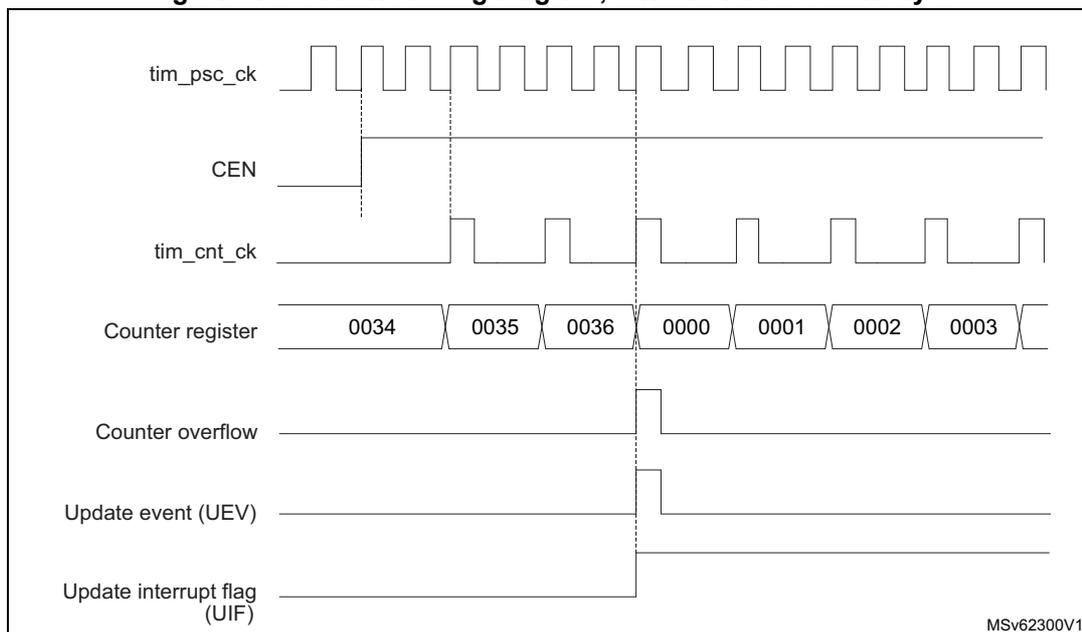
Timing diagram showing the relationship between the prescaler clock (tim_psc_ck), counter enable (CEN), counter clock (tim_cnt_ck), counter register values, counter overflow, update event (UEV), and update interrupt flag (UIF) when the internal clock is divided by 2.
The diagram illustrates the following signals and their timing:
- tim_psc_ck : Prescaler clock signal, shown as a continuous square wave.
- CEN : Counter Enable signal, which goes high to enable counting.
- tim_cnt_ck : Counter clock signal, which is the prescaler clock divided by 2.
- Counter register : Shows the counter values incrementing from 0034 to 0035, 0036, 0000, 0001, 0002, 0003.
- Counter overflow : A pulse generated when the counter reaches its maximum value (0036 in this sequence).
- Update event (UEV) : A pulse generated when the counter overflows.
- Update interrupt flag (UIF) : A pulse generated when the counter overflows.
MSv62300V1
Figure 452. Counter timing diagram, internal clock divided by 4
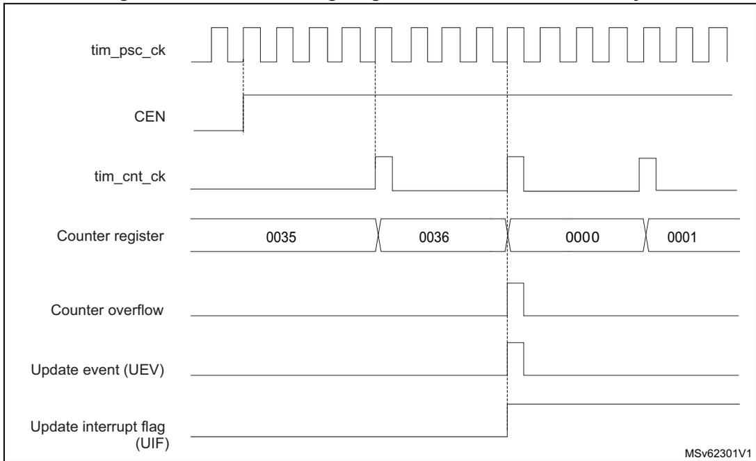
This timing diagram illustrates the operation of a timer when the internal clock is divided by 4. The top signal, tim_psc_ck , is a periodic square wave. Below it, the CEN (Counter Enable) signal is shown as a high-level pulse. The tim_cnt_ck signal is a square wave with a frequency one-fourth that of tim_psc_ck . The Counter register displays a sequence of values: 0035, 0036, 0000, and 0001. The Counter overflow signal is a short pulse that occurs when the counter transitions from 0036 to 0000. The Update event (UEV) is a pulse that coincides with the counter overflow. The bottom signal, Update interrupt flag (UIF) , is a pulse that also coincides with the counter overflow. A small identifier MSv62301V1 is located in the bottom right corner.
Figure 453. Counter timing diagram, internal clock divided by N
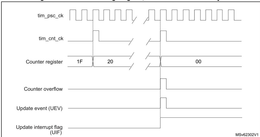
This timing diagram illustrates the operation of a timer when the internal clock is divided by an arbitrary value N. The top signal, tim_psc_ck , is a periodic square wave. Below it, the tim_cnt_ck signal is a square wave with a frequency that is 1/N of the tim_psc_ck frequency. The Counter register displays values in hexadecimal: 1F, 20, and 00. The Counter overflow signal is a short pulse that occurs when the counter transitions from 20 to 00. The Update event (UEV) is a pulse that coincides with the counter overflow. The bottom signal, Update interrupt flag (UIF) , is a pulse that also coincides with the counter overflow. A small identifier MSv62302V1 is located in the bottom right corner.
Figure 454. Counter timing diagram, Update event when ARPE = 0 (TIMx_ARR not preloaded)
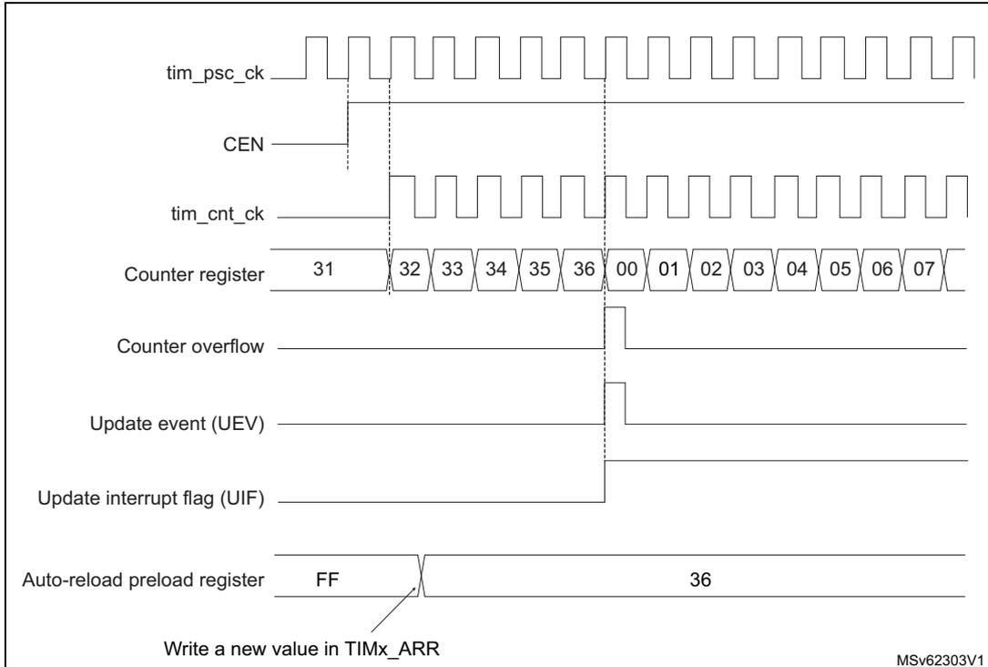
The timing diagram illustrates the operation of a general-purpose timer. The top signal, tim_psc_ck , is a periodic clock. Below it, CEN (Counter Enable) is shown as a high-level signal. The tim_cnt_ck signal is a clock derived from tim_psc_ck . The Counter register displays a sequence of values: 31, 32, 33, 34, 35, 36, 00, 01, 02, 03, 04, 05, 06, 07. A Counter overflow pulse occurs when the counter reaches 36. The Update event (UEV) and Update interrupt flag (UIF) are shown as pulses that occur at the overflow point. The Auto-reload preload register initially contains the value FF. An arrow labeled "Write a new value in TIMx_ARR" points to a transition where the value changes to 36. The diagram is identified by the code MSV62303V1.
Figure 455. Counter timing diagram, Update event when ARPE = 1 (TIMx_ARR preloaded)
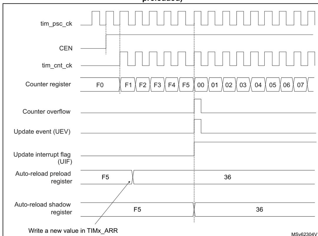
The timing diagram illustrates the operation of a general-purpose timer in up-counting mode with the ARPE bit set. The signals shown are:
- tim_psc_ck : Prescaler clock signal, a continuous square wave.
- CEN : Counter Enable signal, which goes high to start counting.
- tim_cnt_ck : Counter clock signal, which is the prescaled version of tim_psc_ck.
- Counter register : Shows the counter values: F0, F1, F2, F3, F4, F5, 00, 01, 02, 03, 04, 05, 06, 07. The counter increments by 1 at each tim_cnt_ck rising edge.
- Counter overflow : A pulse generated when the counter reaches 00 from F5.
- Update event (UEV) : A pulse generated at the counter overflow.
- Update interrupt flag (UIF) : A pulse generated at the UEV.
- Auto-reload preload register : Shows the value F5 being updated to 36.
- Auto-reload shadow register : Shows the value F5 being updated to 36.
- Write a new value in TIMx_ARR : An arrow pointing to the update of the auto-reload preload register.
MSV62304V1
Down-counting mode
In down-counting mode, the counter counts from the autoreload value (content of the TIMx_ARR register) down to 0, then restarts from the autoreload value and generates a counter underflow event.
An update event can be generated at each counter underflow or by setting the UG bit in the TIMx_EGR register (by software or by using the slave mode controller)
The UEV update event can be disabled by software by setting the UDIS bit in TIMx_CR1 register. This is to avoid updating the shadow registers while writing new values in the preload registers. Then no update event occurs until UDIS bit has been written to 0. However, the counter restarts from the current autoreload value, whereas the counter of the prescaler restarts from 0 (but the prescale rate does not change).
In addition, if the URS bit (update request selection) in TIMx_CR1 register is set, setting the UG bit generates an update event UEV but without setting the UIF flag (thus no interrupt or DMA request is sent). This is to avoid generating both update and capture interrupts when clearing the counter on the capture event.
When an update event occurs, all the registers are updated and the update flag (UIF bit in TIMx_SR register) is set (depending on the URS bit):
- • The buffer of the prescaler is reloaded with the preload value (content of the TIMx_PSC register).
- • The autoreload active register is updated with the preload value (content of the TIMx_ARR register). Note that the autoreload is updated before the counter is reloaded, so that the next period is the expected one.
The following figures show some examples of the counter behavior for different clock frequencies when TIMx_ARR = 0x36.
Figure 456. Counter timing diagram, internal clock divided by 1
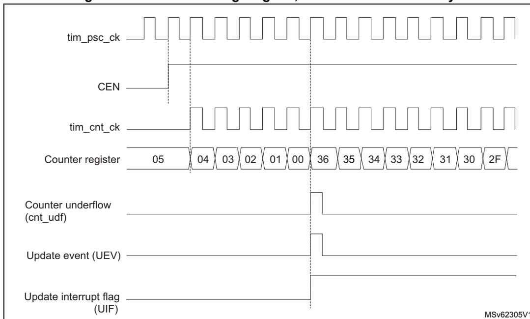
The timing diagram shows the following signals and their behavior:
- tim_psc_ck : Prescaler clock signal, shown as a square wave.
- CEN : Counter Enable signal, which is active low. It is shown as a high level signal.
- tim_cnt_ck : Counter clock signal, which is the output of the prescaler. It is shown as a square wave.
- Counter register : The value of the counter register. It starts at 05, counts down to 00, then reloads to 36 and counts down to 2F. The values 04, 03, 02, 01, 00, 36, 35, 34, 33, 32, 31, 30, and 2F are shown in sequence.
- Counter underflow (cnt_udf) : A signal that goes high when the counter reaches 00 and reloads to 36.
- Update event (UEV) : A signal that goes high when the counter reaches 00 and reloads to 36.
- Update interrupt flag (UIF) : A signal that goes high when the counter reaches 00 and reloads to 36.
The diagram is labeled with MSv62305V1 in the bottom right corner.
Figure 457. Counter timing diagram, internal clock divided by 2
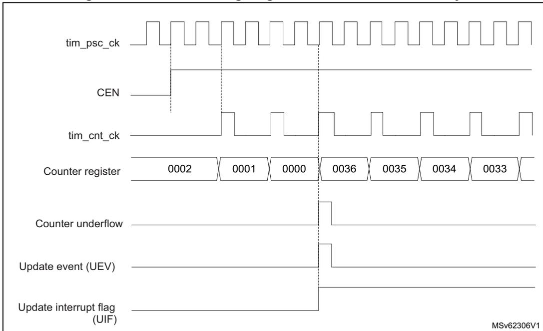
This timing diagram illustrates the operation of a general-purpose timer with the internal clock divided by 2. The top signal, tim_psc_ck , is a high-frequency square wave. Below it, the CEN (Counter Enable) signal is shown as a high-level pulse. The tim_cnt_ck signal is a square wave with a frequency half that of tim_psc_ck . The Counter register displays a sequence of values: 0002, 0001, 0000, 0036, 0035, 0034, 0033. The Counter underflow signal is a short pulse that goes high when the counter reaches 0000 and then returns low. The Update event (UEV) is a pulse that goes high at the underflow and returns low. The Update interrupt flag (UIF) is a pulse that goes high at the underflow and returns low. The diagram is labeled MSv62306V1.
Figure 458. Counter timing diagram, internal clock divided by 4
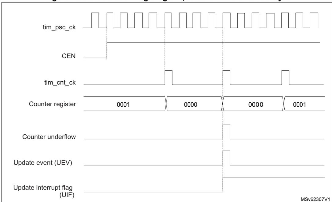
This timing diagram illustrates the operation of a general-purpose timer with the internal clock divided by 4. The top signal, tim_psc_ck , is a high-frequency square wave. Below it, the CEN (Counter Enable) signal is shown as a high-level pulse. The tim_cnt_ck signal is a square wave with a frequency one-quarter that of tim_psc_ck . The Counter register displays a sequence of values: 0001, 0000, 0000, 0001. The Counter underflow signal is a short pulse that goes high when the counter reaches 0000 and then returns low. The Update event (UEV) is a pulse that goes high at the underflow and returns low. The Update interrupt flag (UIF) is a pulse that goes high at the underflow and returns low. The diagram is labeled MSv62307V1.
Figure 459. Counter timing diagram, internal clock divided by N
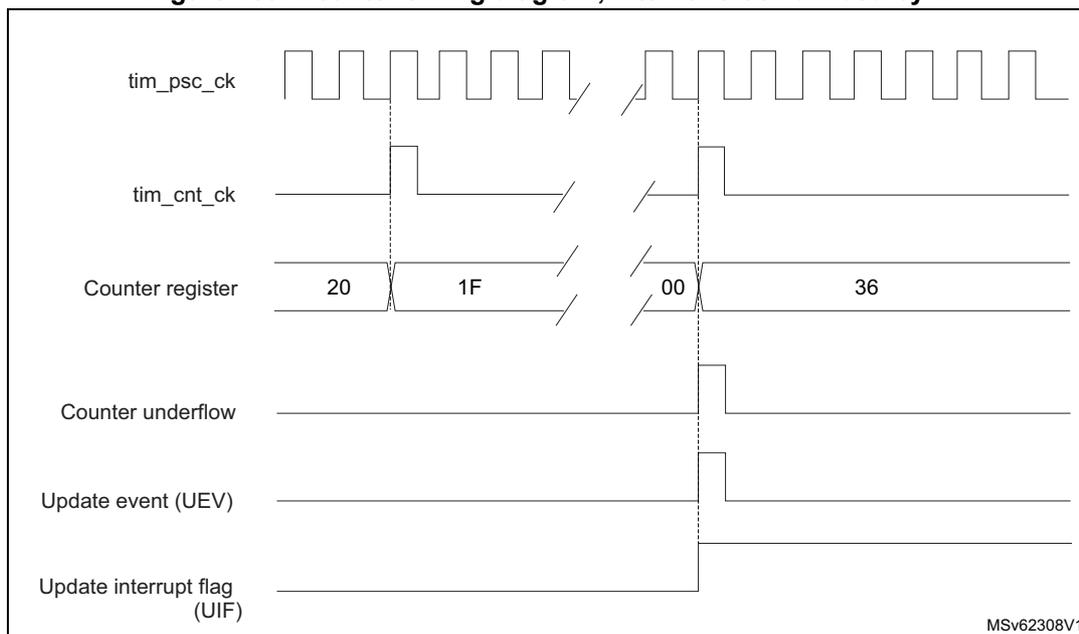
This timing diagram shows the relationship between the prescaler clock, counter clock, and update events during down-counting with a clock division.
- tim_psc_ck : The internal clock signal before prescaling.
- tim_cnt_ck : The counter clock signal, which is the prescaled version of tim_psc_ck.
- Counter register : The current value of the counter. It shows a transition from 20 to 1F, and later from 00 to 36.
- Counter underflow : A pulse generated when the counter reaches zero.
- Update event (UEV) : A pulse generated simultaneously with the counter underflow.
- Update interrupt flag (UIF) : A status flag that is set (goes high) when an update event occurs.
MSv62308V1
Figure 460. Counter timing diagram, Update event
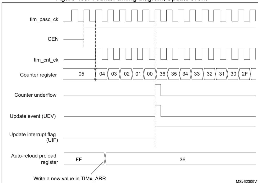
This timing diagram illustrates the update event mechanism when a new value is written to the auto-reload register (TIMx_ARR) during down-counting.
- tim_psc_ck : The internal clock signal.
- CEN : Counter Enable signal.
- tim_cnt_ck : The resulting counter clock.
- Counter register : Shows the down-counting sequence: 05 → 04 → 03 → 02 → 01 → 00. Upon reaching 00, it reloads with the value 36 and continues: 36 → 35 → 34 → 33 → 32 → 31 → 30 → 2F.
- Counter underflow : A pulse triggered when the counter reaches 00.
- Update event (UEV) : A pulse triggered when the counter reaches 00, causing the preload value to be transferred to the active register.
- Update interrupt flag (UIF) : Latches high on the update event.
- Auto-reload preload register : Initially holds FF. A write to TIMx_ARR changes this value to 36. This new value is loaded into the counter at the next update event.
Write a new value in TIMx_ARR
MSv62309V1
Center-aligned mode (up/down-counting)
In center-aligned mode, the counter counts from 0 to the autoreload value (content of the TIMx_ARR register) – 1, generates a counter overflow event, then counts from the
autoreload value down to 1 and generates a counter underflow event. Then it restarts counting from 0.
Center-aligned mode is active when the CMS bits in TIMx_CR1 register are not equal to 00. The output compare interrupt flag of channels configured in output is set when: the counter counts down (Center aligned mode 1, CMS = 01), the counter counts up (Center aligned mode 2, CMS = 10) the counter counts up and down (Center aligned mode 3, CMS = 11).
In this mode, the direction bit (DIR from TIMx_CR1 register) cannot be written. It is updated by hardware and gives the current direction of the counter.
The update event can be generated at each counter overflow and at each counter underflow or by setting the UG bit in the TIMx_EGR register (by software or by using the slave mode controller) also generates an update event. In this case, the counter restarts counting from 0, as well as the counter of the prescaler.
The UEV update event can be disabled by software by setting the UDIS bit in TIMx_CR1 register. This is to avoid updating the shadow registers while writing new values in the preload registers. Then no update event occurs until the UDIS bit has been written to 0. However, the counter continues counting up and down, based on the current autoreload value.
In addition, if the URS bit (update request selection) in TIMx_CR1 register is set, setting the UG bit generates an update event UEV but without setting the UIF flag (thus no interrupt or DMA request is sent). This is to avoid generating both update and capture interrupts when clearing the counter on the capture event.
When an update event occurs, all the registers are updated and the update flag (UIF bit in TIMx_SR register) is set (depending on the URS bit):
- • The buffer of the prescaler is reloaded with the preload value (content of the TIMx_PSC register).
- • The autoreload active register is updated with the preload value (content of the TIMx_ARR register). Note that if the update source is a counter overflow, the autoreload is updated before the counter is reloaded, so that the next period is the expected one (the counter is loaded with the new value).
The following figures show some examples of the counter behavior for different clock frequencies.
Figure 461. Counter timing diagram, internal clock divided by 1, TIMx_ARR = 0x6
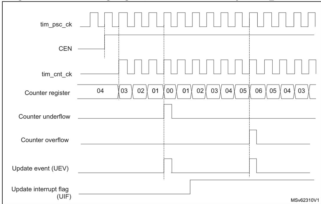
This timing diagram illustrates the operation of a general-purpose timer in center-aligned mode 1 with an internal clock divided by 1 and an auto-reload register (TIMx_ARR) set to 0x6. The diagram shows the following signals over time:
- tim_psc_ck : The prescaler clock signal, shown as a continuous square wave.
- CEN : The counter enable signal, which is active-low. It is shown as a low-level signal after an initial high pulse.
- tim_cnt_ck : The counter clock signal, which is the output of the prescaler and is in phase with tim_psc_ck.
- Counter register : A sequence of values: 04, 03, 02, 01, 00, 01, 02, 03, 04, 05, 06, 05, 04, 03. The counter counts down from 04 to 00, then up to 06, and then back down.
- Counter underflow : A signal that goes high when the counter reaches 00 and then counts up.
- Counter overflow : A signal that goes high when the counter reaches the ARR value of 0x6 and then counts down.
- Update event (UEV) : A pulse that occurs when either the underflow or overflow condition is met.
- Update interrupt flag (UIF) : A flag that is set by the UEV and remains high until it is manually cleared.
- 1. Here, center-aligned mode 1 is used (for more details refer to Section 38.5.1: TIMx control register 1 (TIMx_CR1)(x = 2 to 4) ).
Figure 462. Counter timing diagram, internal clock divided by 2
This timing diagram illustrates the operation of a general-purpose timer in center-aligned mode 1 with an internal clock divided by 2 and an auto-reload register (TIMx_ARR) set to 0x6. The diagram shows the following signals over time:
- tim_psc_ck : The prescaler clock signal, shown as a continuous square wave.
- CEN : The counter enable signal, which is active-low. It is shown as a low-level signal after an initial high pulse.
- tim_cnt_ck : The counter clock signal, which is half the frequency of tim_psc_ck.
- Counter register : A sequence of values: 0003, 0002, 0001, 0000, 0001, 0002, 0003. The counter counts down from 0003 to 0000, then up to 0003.
- Counter underflow : A signal that goes high when the counter reaches 0000 and then counts up.
- Update event (UEV) : A pulse that occurs when the underflow condition is met.
- Update interrupt flag (UIF) : A flag that is set by the UEV and remains high until it is manually cleared.
Figure 463. Counter timing diagram, internal clock divided by 4, TIMx_ARR = 0x36
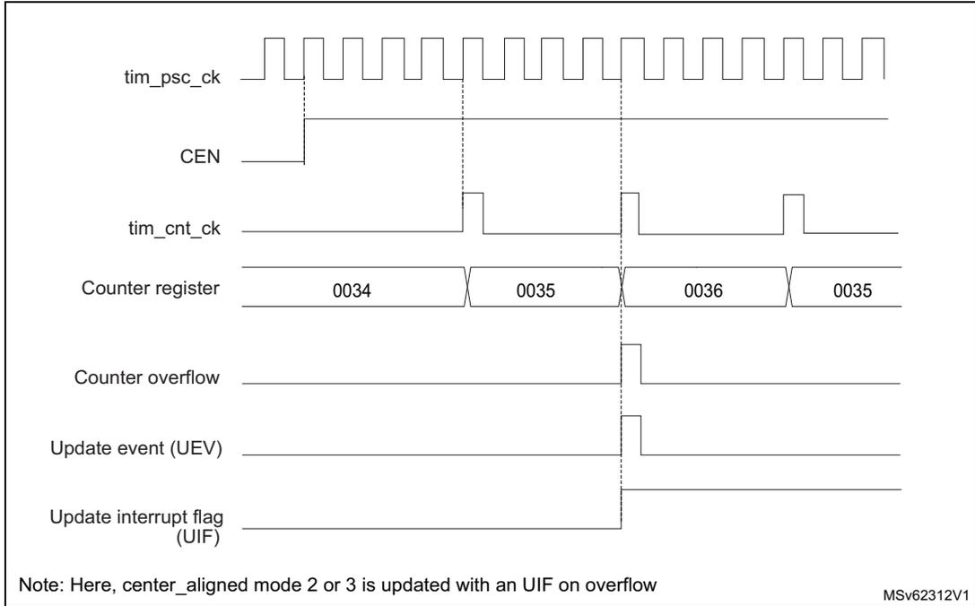
This timing diagram illustrates the operation of a general-purpose timer in center-aligned mode. The tim_psc_ck signal is a high-frequency square wave. The CEN (Counter Enable) signal is a horizontal line that goes high to enable the counter. The tim_cnt_ck signal is a lower-frequency square wave, derived from the prescaler output. The Counter register shows a sequence of values: 0034, 0035, 0036, and 0035. The Counter overflow signal is a pulse that goes high when the counter reaches 0036. The Update event (UEV) and Update interrupt flag (UIF) are also pulses that go high at the overflow point. A note at the bottom left states: "Note: Here, center_aligned mode 2 or 3 is updated with an UIF on overflow". The diagram is labeled MSv62312V1 in the bottom right corner.
- 1. Center-aligned mode 2 or 3 is used with a UIF on overflow.
Figure 464. Counter timing diagram, internal clock divided by N
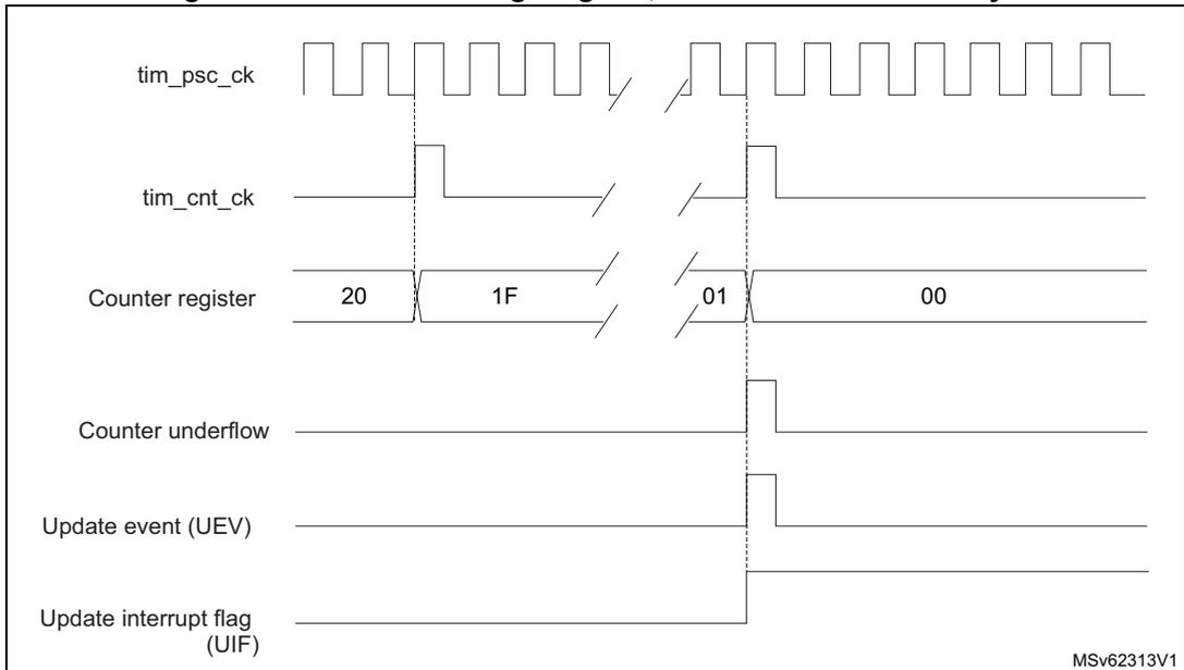
This timing diagram illustrates the operation of a general-purpose timer in center-aligned mode with a prescaler division of N. The tim_psc_ck signal is a square wave. The tim_cnt_ck signal is a lower-frequency square wave. The Counter register shows a sequence of values: 20, 1F, 01, and 00. The Counter underflow signal is a pulse that goes high when the counter reaches 00. The Update event (UEV) and Update interrupt flag (UIF) are also pulses that go high at the underflow point. The diagram is labeled MSv62313V1 in the bottom right corner.
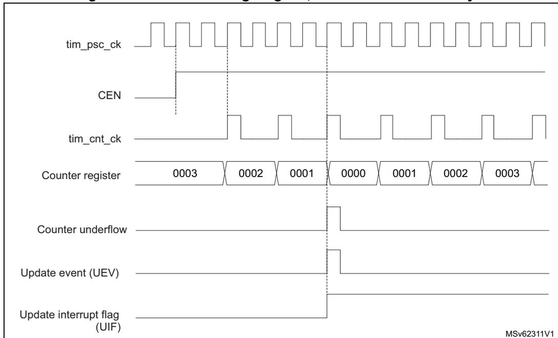
Figure 465. Counter timing diagram, Update event with ARPE = 1 (counter underflow)
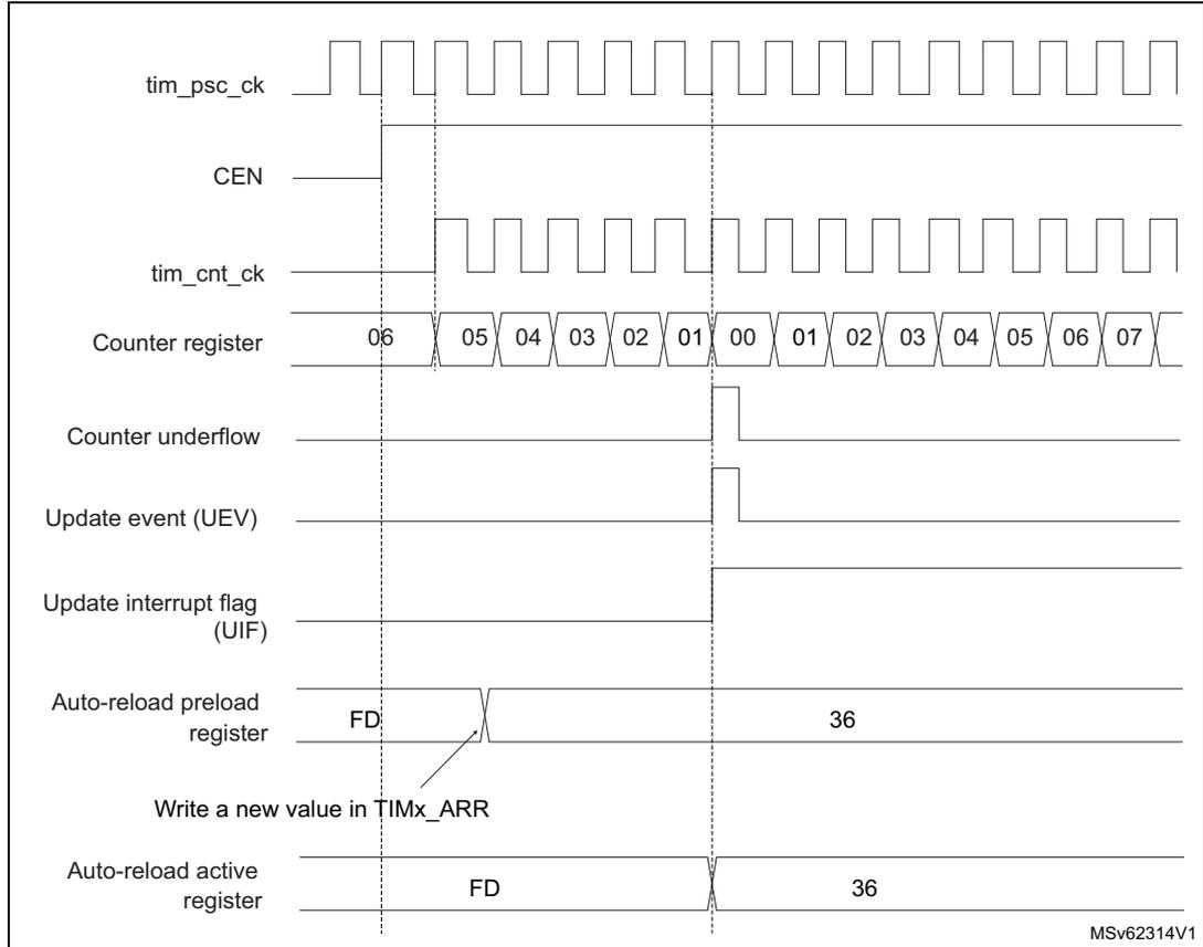
The timing diagram illustrates the operation of a general-purpose timer (TIM2/TIM3/TIM4) with the Auto-reload Preload Enable (ARPE) bit set to 1. The diagram shows the following signals and their timing relationships:
- tim_psc_ck : Prescaler clock signal, shown as a continuous square wave.
- CEN : Counter Enable signal, which is high to enable counting.
- tim_cnt_ck : Counter clock signal, derived from tim_psc_ck.
- Counter register : Shows the counter value counting down from 06 to 00, then rolling over to 01 and continuing up to 07. The underflow from 00 to 01 is highlighted.
- Counter underflow : A pulse that goes high when the counter reaches 00 and rolls over to 01.
- Update event (UEV) : A pulse that goes high upon the counter underflow.
- Update interrupt flag (UIF) : A flag that is set (goes high) by the update event.
- Auto-reload preload register : Contains the value 36. It is initially in a 'FD' (Full Dump) state. An arrow indicates a write to 'TIMx_ARR'.
- Auto-reload active register : Contains the value 36. It is initially in a 'FD' state and updates to the value 36 at the time of the update event.
The diagram shows that when ARPE = 1, the auto-reload value is updated from the preload register to the active register at the time of the update event (counter underflow). The counter then continues counting from 01 up to the new auto-reload value of 36.
MSv62314V1
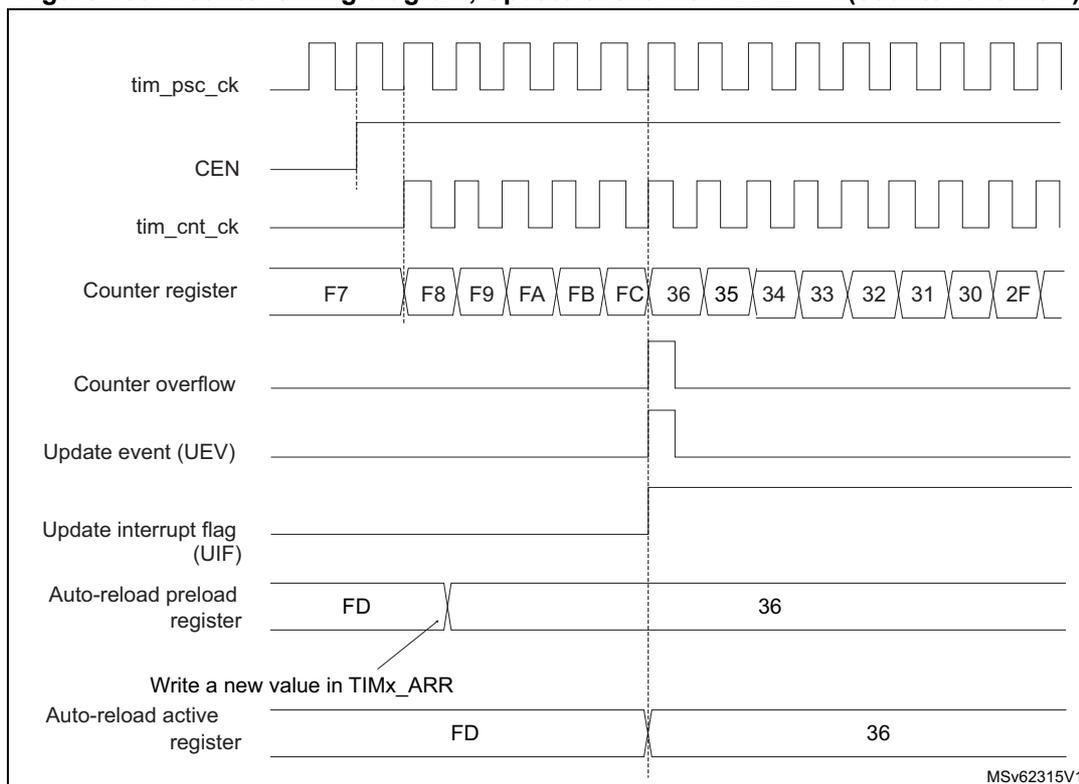
Figure 466. Counter timing diagram, Update event with ARPE = 1 (counter overflow)
38.4.5 Clock selection
The counter clock can be provided by the following clock sources:
- • Internal clock (tim_ker_ck).
- • External clock mode1: external input pin (tim_ti1 or tim_ti2).
- • External clock mode2: external trigger input (tim_etr_in).
- • Internal trigger inputs (tim_itr): using one timer as prescaler for another timer, for example, timer 1 can be configured to act as a prescaler for timer 2. Refer to Using one timer as prescaler for another timer for more details.
Internal clock source (tim_ker_ck)
If the slave mode controller is disabled (SMS = 000 in the TIMx_SMCR register), then the CEN, DIR (in the TIMx_CR1 register), and UG bits (in the TIMx_EGR register) are actual control bits and can be changed only by software (except UG which remains cleared automatically). As soon as the CEN bit is written to 1, the prescaler is clocked by the internal clock tim_ker_ck.
Figure 467 shows the behavior of the control circuit and the upcounter in normal mode, without prescaler.
Figure 467. Control circuit in normal mode, internal clock divided by 1
External clock source mode 1
This mode is selected when SMS = 111 in the TIMx_SMCR register. The counter can count at each rising or falling edge on a selected input.
Figure 468. tim_ti2 external clock connection example
![Block diagram for Figure 468 showing the connection of tim_ti2 external clock source. It includes TIMx_TISEL (TI2SEL[3:0]), TIM_CH2 (tim_ti2_in[15:0]), Filter (ICF[3:0]), Edge detector (tim_ti2f_rising, tim_ti2f_falling), CC2P (TIMx_CCER), TIMx_SMCR (TS[4:0]), Encoder mode, External clock mode 1, External clock mode 2, Internal clock mode, ECE, SMS[2:0], and tim_psc_ck output.](/RM0487-STM32U3/328d99e9bee2665edbd5caa4ac7dcd9e_img.jpg)
- 1. Codes ranging from 01000 to 11111: tim_itr[15:0].
For example, to configure the upcounter to count in response to a rising edge on the tim_ti2 input, use the following procedure:
- 1. Select the proper tim_ti2_in[15:0] source (internal or external) with the TI2SEL[3:0] bits in the TIMx_TISEL register.
- 2. Configure channel 2 to detect rising edges on the tim_ti2 input by writing CC2S= 01 in the TIMx_CCMR1 register.
- 3. Configure the input filter duration by writing the IC2F[3:0] bits in the TIMx_CCMR1 register (if no filter is needed, keep IC2F = 0000).
Note: The capture prescaler is not used for triggering, so it does not need to be configured.
- 4. Select rising edge polarity by writing CC2P = 0 and CC2NP = 0 in the TIMx_CCER register.
- 5. Configure the timer in external clock mode 1 by writing SMS = 111 in the TIMx_SMCR register.
- 6. Select tim_ti2 as the input source by writing TS = 00110 in the TIMx_SMCR register.
- 7. Enable the counter by writing CEN = 1 in the TIMx_CR1 register.
When a rising edge occurs on tim_ti2, the counter counts once and the TIF flag is set.
The delay between the rising edge on tim_ti2 and the actual clock of the counter is due to the resynchronization circuit on tim_ti2 input.
Figure 469. Control circuit in external clock mode 1
The diagram illustrates the timing for external clock mode 1. It shows five horizontal signal lines over time. The top line, 'tim_ti2', shows a periodic square wave. The second line, 'CEN', is a signal that goes high and stays high. The third line, 'tim_cnt_ck, tim_psc_ck', shows narrow pulses that occur at the rising edges of the 'tim_ti2' signal. The fourth line, 'Counter register', shows the count values 34, 35, and 36, which increment at each rising edge of 'tim_ti2'. The bottom line, 'TIF', shows a pulse that goes high at each rising edge of 'tim_ti2' and returns low when 'Write TIF=0' is indicated by an arrow. Vertical dashed lines mark the rising edges of 'tim_ti2' and the corresponding counter increments. The diagram is labeled 'MSv62319V1' in the bottom right corner.
External clock source mode 2
This mode is selected by writing ECE = 1 in the TIMx_SMCR register.
The counter can count at each rising or falling edge on the external trigger input tim_etr_in.
Figure 470 gives an overview of the external trigger input block.
Figure 470. External trigger input block
![Figure 470. External trigger input block diagram. The diagram shows the signal flow from the external trigger input (TIMx_ETR) through a multiplexer (TIMx_AF1[17:14]) to a filter downcounter. The filter downcounter is controlled by the TIMx_SMCR register (ETP, ETPS[1:0], ETF[3:0]). The output of the filter downcounter (tim_etrp) is divided by a divider (/1, /2, /4, /8) controlled by the TIMx_SMCR register (ETPS[1:0]). The output of the divider (tim_etrp) is then passed to a filter downcounter (tim_etrp) controlled by the TIMx_SMCR register (ETF[3:0]). The output of the filter downcounter (tim_etrp) is then passed to a multiplexer (Encoder mode, External clock mode 1, External clock mode 2, Internal clock mode) controlled by the TIMx_SMCR register (ECE, SMS[2:0]). The output of the multiplexer (tim_psc_ck) is the final output. The diagram also shows the internal clock (tim_ker_ck) and the external trigger input (tim_etr_in) signals.](/RM0487-STM32U3/bdd26457cc57f4fa44e2ac9908c6467d_img.jpg)
The diagram illustrates the external trigger input block for general-purpose timers. It shows the signal path from the external trigger input (TIMx_ETR) through various processing stages. The input is first multiplexed by TIMx_AF1[17:14] to produce tim_etr_in. This signal is then processed by a filter downcounter (tim_etrp) which is controlled by the TIMx_SMCR register (ETP, ETPS[1:0], ETF[3:0]). The output of the filter downcounter is divided by a divider (/1, /2, /4, /8) controlled by the TIMx_SMCR register (ETPS[1:0]). The output of the divider (tim_etrp) is then passed to a multiplexer (Encoder mode, External clock mode 1, External clock mode 2, Internal clock mode) controlled by the TIMx_SMCR register (ECE, SMS[2:0]). The output of the multiplexer (tim_psc_ck) is the final output. The diagram also shows the internal clock (tim_ker_ck) and the external trigger input (tim_etr_in) signals.
For example, to configure the upcounter to count each two rising edges on tim_etr_in, use the following procedure:
- 1. Select the proper tim_etr_in source (internal or external) with the ETRSEL[3:0] bits in the TIMx_AF1 register.
- 2. As no filter is needed in this example, write ETF[3:0] = 0000 in the TIMx_SMCR register.
- 3. Set the prescaler by writing ETPS[1:0] = 01 in the TIMx_SMCR register.
- 4. Select rising edge detection on the tim_etr_in by writing ETP = 0 in the TIMx_SMCR register.
- 5. Enable external clock mode 2 by writing ECE = 1 in the TIMx_SMCR register.
- 6. Enable the counter by writing CEN = 1 in the TIMx_CR1 register.
The counter counts once each two tim_etr_in rising edges.
The delay between the rising edge on tim_etr_in and the actual clock of the counter is due to the resynchronization circuit on the tim_etrp signal. As a consequence, the maximum frequency that can be correctly captured by the counter is at most 1/4 of tim_ker_ck frequency. When the ETRP signal is faster, the user must apply a division of the external signal by a proper ETPS prescaler setting.
Figure 471. Control circuit in external clock mode 2
The diagram shows the relationship between several signals over time. tim_ker_ck is a periodic square wave. CEN is a high-active enable signal. tim_etr_in and tim_etrp are external trigger signals. tim_etrfl is a filtered version of tim_etr_in . tim_cnt_ck and tim_psc_ck are clock signals for the counter and prescaler. The Counter register shows values 34, 35, and 36. Vertical dashed lines indicate that the counter increments (34 to 35, 35 to 36) on the rising edges of tim_etrp when CEN is high and tim_ker_ck is active.
38.4.6 Capture/compare channels
Each Capture/Compare channel is built around a capture/compare register (including a shadow register), an input stage for capture (with digital filter, multiplexing and prescaler) and an output stage (with comparator and output control).
The following figure gives an overview of one Capture/Compare channel.
The input stage samples the corresponding tim_tix input to generate a filtered signal tim_tixf . Then, an edge detector with polarity selection generates a signal ( tim_tixfpy ) which can be used as trigger input by the slave mode controller or as the capture command. It is prescaled before the capture register ( ICxPS ).
Figure 472. Capture/compare channel (example: channel 1 input stage)
This block diagram illustrates the input stage of a capture/compare channel (Channel 1). The input TIM_CH1 or tim_ti1_in[15:1] is selected by TIMx_TISEL (TI1SEL[3:0]). This signal passes through a Filter downcounter (controlled by ICF[3:0] and TIMx_CCMR1 ) to produce tim_ti1f . An Edge detector then generates tim_ti1f_rising and tim_ti1f_falling signals. These are combined via an OR gate to produce tim_ti1f_ed , which is sent to the slave mode controller. A multiplexer selects between tim_ti1_f (from the edge detector) and tim_ti2fp1 (from channel 2) based on CC1P/CC1NP . The selected signal passes through another multiplexer (selecting between tim_trc from the slave mode controller and tim_ti2fp1 ) to produce tim_ic1 . This signal is then divided by a Divider (1, 2, 4, 8) controlled by ICPS[1:0] and TIMx_CCMR1 to produce the final input tim_ic1f . The CC1E bit in TIMx_CCER enables the input stage.
The output stage generates an intermediate waveform which is then used for reference:
tim_ocxref
(active high). The polarity acts at the end of the chain.
Figure 473. Capture/compare channel 1 main circuit
![Figure 473: Capture/compare channel 1 main circuit diagram. The diagram shows the internal logic of the capture/compare channel. At the top, an APB Bus connects to an MCU-peripheral interface. This interface connects to a 16/32-bit Capture/compare preload register and a compare shadow register. A Counter is connected to both registers. In Input mode, signals CC1S[1], CC1S[0], IC1PS, CC1E, CC1G, and TIMx_EGR are used to control the capture process. In Output mode, signals CC1S[1], CC1S[0], OC1PE, UEV (from time base unit), and TIMx_CCMR1 are used to control the output process. A Comparator compares the Counter value with the compare shadow register value, outputting CNT>CCR1 and CNT=CCR1 signals.](/RM0487-STM32U3/44a916cd2b9b2c80bab1080f39afd1f6_img.jpg)
Figure 474. Output stage of capture/compare channel (channel 1, idem ch.2, 3 and 4)
![Figure 474: Output stage of capture/compare channel diagram. This diagram details the output stage logic. It starts with TIMx_SMCR and OCCS(1) controlling a multiplexer that selects between tim_ocref_clr and tim_etrif. The output of this multiplexer is tim_ocref_clr_int. This signal, along with CNT > CCR1, CNT = CCR1, and tim_oc2ref, is input to the Output mode controller. The controller outputs tim_oc1ref, which is then processed by an Output selector. The Output selector also takes inputs from OC1CE and OC1M[3:0] from TIMx_CCMR1. The output of the selector is tim_oc1refc, which is connected to the master mode controller and also to a multiplexer. This multiplexer selects between '0' and the output of an inverter. The inverter's input is controlled by CC1E and CC1P from TIMx_CCER. The output of the multiplexer is then processed by an Output enable circuit, which is controlled by CC1E from TIMx_CCER. The final output is tim_oc1.](/RM0487-STM32U3/8d44443536c7300a92837c192382aa1b_img.jpg)
1. Available on some instances only. If not available,
tim_etrif
is directly connected to
tim_ocref_clr_int
.
The capture/compare block is made of one preload register and one shadow register. Write and read always access the preload register.
In capture mode, captures are actually done in the shadow register, which is copied into the preload register.
In compare mode, the content of the preload register is copied into the shadow register which is compared to the counter.
38.4.7 Input capture mode
In input capture mode, the capture/compare registers (TIMx_CCRx) are used to latch the value of the counter after a transition detected by the corresponding ICx signal. When a capture occurs, the corresponding CCxIF flag (TIMx_SR register) is set and an interrupt or a DMA request can be sent if they are enabled. If a capture occurs while the CCxIF flag was already high, then the overcapture flag CCxOF (TIMx_SR register) is set. CCxIF can be cleared by software by writing it to 0 or by reading the captured data stored in the TIMx_CCRx register. CCxOF is cleared when it is written with 0.
The following example shows how to capture the counter value in TIMx_CCR1 when tim_ti1 input rises. To do this, use the following procedure:
- 1. Select the proper tim_tix_in[15:0] source (internal or external) with the TI1SEL[3:0] bits in the TIMx_TISEL register.
- 2. Select the active input: TIMx_CCR1 must be linked to the tim_ti1 input, so write the CC1S bits to 01 in the TIMx_CCMR1 register. As soon as CC1S becomes different from 00, the channel is configured in input and the TIMx_CCR1 register becomes read-only.
- 3. Program the needed input filter duration in relation with the signal connected to the timer (when the input is one of the tim_tix (ICxF bits in the TIMx_CCMRx register). Let's imagine that, when toggling, the input signal is not stable during at most five internal clock cycles. We must program a filter duration longer than these five clock cycles. We can validate a transition on tim_ti1 when eight consecutive samples with the new level have been detected (sampled at \( f_{DTS} \) frequency). Then write IC1F bits to 0011 in the TIMx_CCMR1 register.
- 4. Select the edge of the active transition on the tim_ti1 channel by writing the CC1P and CC1NP bits to 000 in the TIMx_CCER register (rising edge in this case).
- 5. Program the input prescaler. In this example, the capture is to be performed at each valid transition, so the prescaler is disabled (write IC1PS bits to 00 in the TIMx_CCMR1 register).
- 6. Enable capture from the counter into the capture register by setting the CC1E bit in the TIMx_CCER register.
- 7. If needed, enable the related interrupt request by setting the CC1IE bit in the TIMx_DIER register, and/or the DMA request by setting the CC1DE bit in the TIMx_DIER register.
When an input capture occurs:
- • The TIMx_CCR1 register gets the value of the counter on the active transition.
- • CC1IF flag is set (interrupt flag). CC1OF is also set if at least two consecutive captures occurred whereas the flag was not cleared.
- • An interrupt is generated depending on the CC1IE bit.
- • A DMA request is generated depending on the CC1DE bit.
In order to handle the overcapture, it is recommended to read the data before the overcapture flag. This is to avoid missing an overcapture which may happen after reading the flag and before reading the data.
Note: IC interrupt and/or DMA requests can be generated by software by setting the corresponding CCxG bit in the TIMx_EGR register.
38.4.8 PWM input mode
This mode is used to measure both the period and the duty cycle of a PWM signal connected to single
tim_tix
input:
- • The
TIMx_CCR1register holds the period value (interval between two consecutive rising edges). - • The
TIMx_CCR2register holds the pulse width (interval between two consecutive rising and falling edges).
This mode is a particular case of input capture mode. The set-up procedure is similar with the following differences:
- • Two
ICxsignals are mapped on the sametim_tixinput. - • These two
ICxsignals are active on edges with opposite polarity. - • One of the two
TIxFPsignals is selected as trigger input and the slave mode controller is configured in reset mode.
The period and the pulse width of a PWM signal applied on
tim_ti1
can be measured using the following procedure:
- 1. Select the proper
tim_tix_in[15:0]source (internal or external) with theTI1SEL[3:0]bits in theTIMx_TISELregister. - 2. Select the active input for
TIMx_CCR1: write theCC1Sbits to 01 in theTIMx_CCMR1register (tim_ti1selected). - 3. Select the active polarity for
tim_ti1fp1(used both for capture inTIMx_CCR1and counter clear): write theCC1Pto 0 and theCC1NPbit to 0 (active on rising edge). - 4. Select the active input for
TIMx_CCR2: write theCC2Sbits to 10 in theTIMx_CCMR1register (tim_ti1selected). - 5. Select the active polarity for
tim_ti1fp2(used for capture inTIMx_CCR2): write theCC2Pbit to 1 and theCC2NPbit to 0 (active on falling edge). - 6. Select the valid trigger input: write the
TSbits to 00101 in theTIMx_SMCRregister (tim_ti1fp1selected). - 7. Configure the slave mode controller in reset mode: write the
SMSbits to 100 in theTIMx_SMCRregister. - 8. Enable the captures: write the
CC1EandCC2Ebits to 1 in theTIMx_CCERregister.
Figure 475. PWM input mode timing
IC1 capture
IC2 capture
reset counter
IC2 capture
pulse width
measurement
IC1 capture
pulse width
measurement
MSv62325V1
- 1. The PWM input mode can be used only with the TIMx_CH1/TIMx_CH2 signals due to the fact that only tim_ti1fp1 and tim_ti2fp2 are connected to the slave mode controller.
38.4.9 Forced output mode
In output mode (CCxS bits = 00 in the TIMx_CCMRx register), each output compare signal (tim_ocxref and then tim_ocx) can be forced to active or inactive level directly by software, independently of any comparison between the output compare register and the counter.
To force an output compare signal (tim_ocxref/tim_ocx) to its active level, the user just needs to write 101 in the OCxM bits in the corresponding TIMx_CCMRx register. Thus tim_ocxref is forced high (tim_ocxref is always active high) and tim_ocx get opposite value to CCxP polarity bit.
For example: CCxP = 0 (tim_ocx active high) => tim_ocx is forced to high level.
tim_ocxref signal can be forced low by writing the OCxM bits to 100 in the TIMx_CCMRx register.
Anyway, the comparison between the TIMx_CCRx shadow register and the counter is still performed and allows the flag to be set. Interrupt and DMA requests can be sent accordingly. This is described in the Output Compare mode section.
38.4.10 Output compare mode
This function is used to control an output waveform or indicating when a period of time has elapsed.
When a match is found between the capture/compare register and the counter, the output compare function:
- • Assigns the corresponding output pin to a programmable value defined by the output compare mode (OCxM bits in the TIMx_CCMRx register) and the output polarity (CCxP bit in the TIMx_CCER register). The output pin can keep its level (OCxM = 000), be set
active (OCxM = 001), be set inactive (OCxM = 010) or can toggle (OCxM = 011) on match.
- • Sets a flag in the interrupt status register (CCxIF bit in the TIMx_SR register).
- • Generates an interrupt if the corresponding interrupt mask is set (CCXIE bit in the TIMx_DIER register).
- • Sends a DMA request if the corresponding enable bit is set (CCxDE bit in the TIMx_DIER register, CCDS bit in the TIMx_CR2 register for the DMA request selection).
The TIMx_CCRx registers can be programmed with or without preload registers using the OCxPE bit in the TIMx_CCMRx register.
In output compare mode, the update event UEV has no effect on tim_ocxref and tim_ocx output. The timing resolution is one count of the counter. Output compare mode can also be used to output a single pulse (in One-pulse mode).
Procedure
- 1. Select the counter clock (internal, external, prescaler).
- 2. Write the desired data in the TIMx_ARR and TIMx_CCRx registers.
- 3. Set the CCxIE and/or CCxDE bits if an interrupt and/or a DMA request is to be generated.
- 4. Select the output mode. For example:
- a) Write OCxM = 0011 to toggle tim_ocx output pin when CNT matches CCRx.
- b) Write OCxPE = 0 to disable preload register.
- c) Write CCxP = 0 to select active high polarity.
- d) Write CCxE = 1 to enable the output.
- 5. Enable the counter by setting the CEN bit in the TIMx_CR1 register.
The TIMx_CCRx register can be updated at any time by software to control the output waveform, provided that the preload register is not enabled (OCxPE = 0, else TIMx_CCRx shadow register is updated only at the next update event UEV). An example is given in Figure 476 .
Figure 476. Output compare mode, toggle on tim_oc1
Write B201h in the CC1R register
CNT: 0039 | 003A | 003B | ... | B200 | B201
CCR1: 003A | B201
tim_oc1ref = tim_oc1
Match detected on CCR1
Interrupt generated if enabled
MSv62326V1
38.4.11 PWM mode
Pulse width modulation mode is used to generate a signal with a frequency determined by the value of the TIMx_ARR register and a duty cycle determined by the value of the TIMx_CCRx register.
The PWM mode can be selected independently on each channel (one PWM per tim_ocx output) by writing 110 (PWM mode 1) or 111 (PWM mode 2) in the OCxM bits in the TIMx_CCMRx register. The corresponding preload register must be enabled by setting the OCxPE bit in the TIMx_CCMRx register, and eventually the autoreload preload register (in up-counting or center-aligned modes) by setting the ARPE bit in the TIMx_CR1 register.
As the preload registers are transferred to the shadow registers only when an update event occurs, before starting the counter, all registers must be initialized by setting the UG bit in the TIMx_EGR register.
tim_ocx polarity is software programmable using the CCxP bit in the TIMx_CCER register. It can be programmed as active high or active low. tim_ocx output is enabled by the CCxE bit in the TIMx_CCER register. Refer to the TIMx_CCERx register description for more details.
In PWM mode (1 or 2), TIMx_CNT and TIMx_CCRx are always compared to determine whether \( TIMx\_CCRx \leq TIMx\_CNT \) or \( TIMx\_CNT \leq TIMx\_CCRx \) (depending on the direction of the counter). The tim_ocref_clr can be cleared by an external event through the tim_etr_in or the tim_ocref_clr signals. In this case the tim_ocref_clr signal is asserted only:
- • After a compare match event.
- • When the output compare mode (OCxM bits in TIMx_CCMRx register) switches from the “frozen” configuration (no comparison, OCxM = 000) to one of the PWM modes (OCxM = 110 or 111). This forces the PWM by software while the timer is running.
The timer is able to generate PWM in edge-aligned mode or center-aligned mode depending on the CMS bits in the TIMx_CR1 register.
PWM edge-aligned mode
- • Up-counting configuration
- • Up-counting is active when the DIR bit in the TIMx_CR1 register is low. Refer to Up-counting mode .
In the following example, we consider PWM mode 1. The reference PWM signal tim_ocxref is high as long as TIMx_CNT < TIMx_CCRx else it becomes low. If the compare value in TIMx_CCRx is greater than the autoreload value (in TIMx_ARR) then tim_ocxref is held at 1. If the compare value is 0 then tim_ocxref is held at 0. Figure 477 shows some edge-aligned PWM waveforms in an example where TIMx_ARR = 8.
Figure 477. Edge-aligned PWM waveforms (ARR = 8)
The figure is a timing diagram illustrating edge-aligned PWM waveforms for different compare register (CCR) values. The counter register (TIMx_CNT) is shown at the top, counting from 0 to 8 and then resetting to 0. The diagram is divided into four sections based on the CCRx value:
- CCRx=4: The tim_ocxref signal is high from counter value 0 to 4 and low from 4 to 8. The CCxIF flag is set when the counter reaches 4.
- CCRx=8: The tim_ocxref signal is high from counter value 0 to 8 and low from 8 to 0. The CCxIF flag is set when the counter reaches 8.
- CCRx>8: The tim_ocxref signal is always high. The CCxIF flag is never set.
- CCRx=0: The tim_ocxref signal is always low. The CCxIF flag is never set.
The diagram also shows the counter register values (0, 1, 2, 3, 4, 5, 6, 7, 8, 0, 1) and the corresponding tim_ocxref and CCxIF signals for each CCRx value. The source identifier MSV62327V1 is visible in the bottom right corner.
Down-counting configuration
- • Down-counting is active when DIR bit in TIMx_CR1 register is high. Refer to Down-counting mode .
In PWM mode 1, the reference signal tim_ocxref is low as long as TIMx_CNT > TIMx_CCRx else it becomes high. If the compare value in TIMx_CCRx is greater than the autoreload value in TIMx_ARR, then tim_ocxref is held at 100%. PWM is not possible in this mode.
PWM center-aligned mode
Center-aligned mode is active when the CMS bits in TIMx_CR1 register are different from 00 (all the remaining configurations having the same effect on the tim_ocxref/tim_ocx signals). The compare flag is set when the counter counts up, when it counts down or both when it counts up and down depending on the CMS bits configuration. The direction bit
(DIR) in the TIMx_CR1 register is updated by hardware and must not be changed by software. Refer to Center-aligned mode (up/down-counting) .
Figure 478 shows some center-aligned PWM waveforms in an example where:
- • TIMx_ARR = 8.
- • PWM mode is the PWM mode 1.
- • The flag is set when the counter counts down corresponding to the center-aligned mode 1 selected for CMS = 01 in TIMx_CR1 register.
Figure 478. Center-aligned PWM waveforms (ARR = 8)
The figure illustrates the relationship between the counter register values and the resulting PWM waveforms for different Capture/Compare Register (CCR) values. The counter register values are shown at the top, ranging from 0 to 8 and then back down to 0, with an additional '1' at the end. Vertical dashed lines indicate the counter values 0, 4, 7, 8, 7, 4, 0, and 1. The 'tim_ocref' signal is shown for four cases: CCRx = 4, CCRx = 7, CCRx = 8, and CCRx > 8. For CCRx = 4, the signal is high from counter value 4 to 4. For CCRx = 7, the signal is high from counter value 7 to 7. For CCRx = 8, the signal is high from counter value 8 to 8. For CCRx > 8, the signal is always high. The CCxIF flag status is shown for CMS=01, CMS=10, and CMS=11. Arrows indicate the events that set the CCxIF flag: for CMS=01, it's when the counter counts down to the CCR value; for CMS=10, it's when the counter counts up to the CCR value; for CMS=11, it's when the counter counts down to 0. The diagram also shows the '1' and '0' levels for the tim_ocref signal.
Hints on using center-aligned mode:
- • When starting in center-aligned mode, the current up-down configuration is used. It means that the counter counts up or down depending on the value written in the DIR bit
in the TIMx_CR1 register. Moreover, the DIR and CMS bits must not be changed at the same time by the software.
- • Writing to the counter while running in center-aligned mode is not recommended as it can lead to unexpected results. In particular:
- – The direction is not updated if a value greater than the autoreload value is written in the counter (TIMx_CNT > TIMx_ARR). For example, if the counter was counting up, it continues to count up.
- – The direction is updated if 0 or the TIMx_ARR value is written in the counter but no update event UEV is generated.
- • The safest way to use center-aligned mode is to generate an update by software (setting the UG bit in the TIMx_EGR register) just before starting the counter and not to write the counter while it is running.
Dithering mode
The PWM mode effective resolution can be increased by enabling the dithering mode, using the DITHEN bit in the TIMx_CR1 register. This applies to both the CCR (for duty cycle resolution increase) and ARR (for PWM frequency resolution increase).
The operating principle is to have the actual CCR (or ARR) value slightly changed (adding or not one timer clock period) over 16 consecutive PWM periods, with predefined patterns. This allows a 16-fold resolution increase, considering the average duty cycle or PWM period. Figure 479 presents the dithering principle applied to four consecutive PWM cycles.
Figure 479. Dithering principle
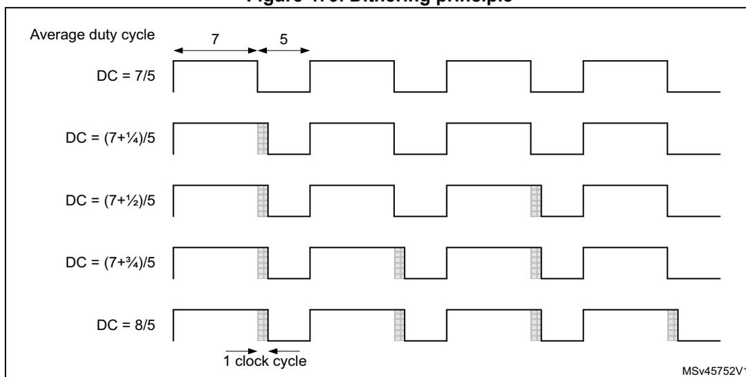
The figure illustrates the dithering principle for PWM. It shows four consecutive PWM cycles. The first cycle has a base duty cycle \( DC = 7/5 \) . The subsequent cycles show the duty cycle being incremented by 1/4, 1/2, and 3/4 of a clock cycle, resulting in average duty cycles \( DC = (7+1/4)/5 \) , \( DC = (7+1/2)/5 \) , and \( DC = (7+3/4)/5 \) . The final cycle shows the duty cycle \( DC = 8/5 \) . A horizontal arrow at the top indicates the average duty cycle over 7 and 5 clock cycles. A horizontal arrow at the bottom indicates a single clock cycle. The diagram is labeled MSV45752V1.
When the dithering mode is enabled, the register coding is changed as following (see Figure 480 for example):
- • The four LSBs are coding for the enhanced resolution part (fractional part).
- • The MSBs are left-shifted by four places and are coding for the base value. In 16-bit mode, the 16-bit format is maintained.
Note: The following sequence must be followed when resetting the DITHEN bit:
- 1. CEN and ARPE bits must be reset.
- 2. The DITHEN bit must be reset.
- 3. The CCIF flags must be cleared.
- 4. The CEN bit can be set (eventually with ARPE = 1).
Figure 480. Data format and register coding in dithering mode
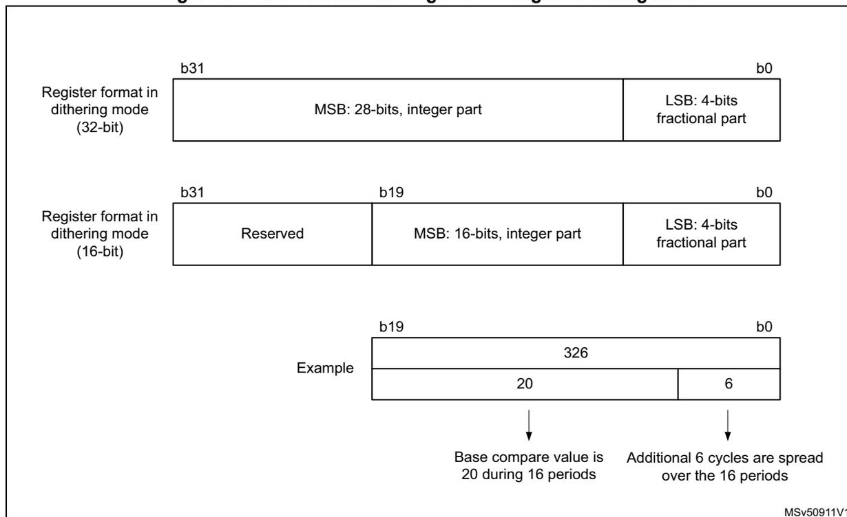
The diagram illustrates the data format and register coding in dithering mode for 32-bit and 16-bit timers.
Register format in dithering mode (32-bit): A 32-bit register with bits b31 to b0. The MSB (Most Significant Bit) is a 28-bit integer part (bits b31 to b4), and the LSB (Least Significant Bit) is a 4-bit fractional part (bits b3 to b0).
Register format in dithering mode (16-bit): A 16-bit register with bits b31 to b0. The first 12 bits (b31 to b20) are Reserved. The next 16 bits (b19 to b4) form the MSB: 16-bits, integer part. The last 4 bits (b3 to b0) form the LSB: 4-bits fractional part.
Example: A 32-bit register value of 326. The integer part (bits b31 to b4) is 20, and the fractional part (bits b3 to b0) is 6. Arrows indicate that the base compare value is 20 during 16 periods, and additional 6 cycles are spread over the 16 periods.
MSv50911V1
The minimum frequency is given by the following formula:
Note: For 16-bit timers, the maximum TIMx_ARR and TIMx_CCRy values are limited to 0xFFFFEF in dithering mode (corresponds to 65534 for the integer part and 15 for the dithered part). For 32-bit timers, the maximum TIMx_ARR and TIMx_CCRy values are limited to
0xFFFFFEF in dithering mode (corresponds to 264435454 for the integer part and 15 for the dithered part).
As shown on Figure 481 and Figure 482 , the dithering mode is used to increase the PWM resolution.
Figure 481. PWM resolution vs frequency (16-bit mode)
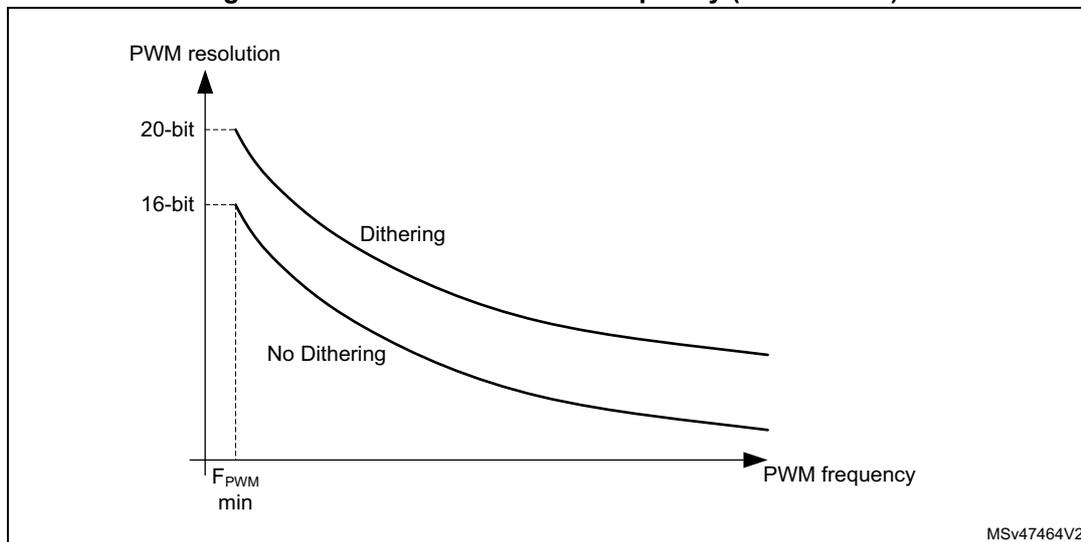
A line graph showing PWM resolution on the y-axis versus PWM frequency on the x-axis for 16-bit mode. The y-axis has two marked points: 16-bit and 20-bit. The x-axis has a marked point \( F_{\text{PWM min}} \) . Two curves are shown: 'Dithering' and 'No Dithering'. The 'Dithering' curve starts at 20-bit resolution and decreases as frequency increases. The 'No Dithering' curve starts at 16-bit resolution and decreases as frequency increases. Both curves are monotonically decreasing. A vertical dashed line at \( F_{\text{PWM min}} \) extends from the x-axis to both curves. The 'Dithering' curve is consistently above the 'No Dithering' curve. The label MSv47464V2 is in the bottom right corner.
Figure 482. PWM resolution vs frequency (32-bit mode)
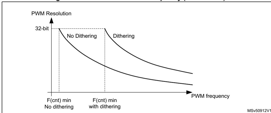
A line graph showing PWM Resolution on the y-axis versus PWM frequency on the x-axis for 32-bit mode. The y-axis has a marked point at 32-bit. The x-axis has two marked points: \( F(\text{cnt}) \text{ min} \) No dithering and \( F(\text{cnt}) \text{ min} \) with dithering. Two curves are shown: 'No Dithering' and 'Dithering'. The 'No Dithering' curve starts at 32-bit resolution and decreases as frequency increases. The 'Dithering' curve starts at 32-bit resolution at the \( F(\text{cnt}) \text{ min} \) with dithering point and decreases as frequency increases. Both curves are monotonically decreasing. Vertical dashed lines extend from the x-axis to the curves at the marked frequency points. The 'Dithering' curve is consistently above the 'No Dithering' curve. The label MSv50912V1 is in the bottom right corner.
The duty cycle and/or period changes are spread over 16 consecutive periods, as described in Figure 483 .
Figure 483. PWM dithering pattern
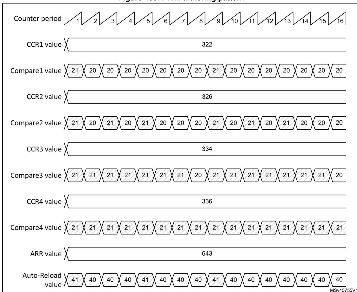
| Parameter | 1 | 2 | 3 | 4 | 5 | 6 | 7 | 8 | 9 | 10 | 11 | 12 | 13 | 14 | 15 | 16 |
|---|---|---|---|---|---|---|---|---|---|---|---|---|---|---|---|---|
| Counter period | 1 | 2 | 3 | 4 | 5 | 6 | 7 | 8 | 9 | 10 | 11 | 12 | 13 | 14 | 15 | 16 |
| CCR1 value | 322 | |||||||||||||||
| Compare1 value | 21 | 20 | 20 | 20 | 20 | 20 | 20 | 20 | 21 | 20 | 20 | 20 | 20 | 20 | 20 | 20 |
| CCR2 value | 326 | |||||||||||||||
| Compare2 value | 21 | 20 | 21 | 20 | 21 | 20 | 20 | 20 | 21 | 20 | 21 | 20 | 21 | 20 | 20 | 20 |
| CCR3 value | 334 | |||||||||||||||
| Compare3 value | 21 | 21 | 21 | 21 | 21 | 21 | 21 | 20 | 21 | 21 | 21 | 21 | 21 | 21 | 21 | 20 |
| CCR4 value | 336 | |||||||||||||||
| Compare4 value | 21 | 21 | 21 | 21 | 21 | 21 | 21 | 21 | 21 | 21 | 21 | 21 | 21 | 21 | 21 | 21 |
| ARR value | 643 | |||||||||||||||
| Auto-Reload value | 41 | 40 | 40 | 40 | 41 | 40 | 40 | 40 | 41 | 40 | 40 | 40 | 40 | 40 | 40 | 40 |
MSV45755V1
The autoreload and compare values increments are spread following specific patterns described in Table 411 . The dithering sequence is done to have increments distributed as evenly as possible and minimize the overall ripple.
Table 411. CCR and ARR register change dithering pattern
| LSB value | PWM period | |||||||||||||||
|---|---|---|---|---|---|---|---|---|---|---|---|---|---|---|---|---|
| 1 | 2 | 3 | 4 | 5 | 6 | 7 | 8 | 9 | 10 | 11 | 12 | 13 | 14 | 15 | 16 | |
| 0000 | - | - | - | - | - | - | - | - | - | - | - | - | - | - | - | - |
| 0001 | +1 | - | - | - | - | - | - | - | - | - | - | - | - | - | - | - |
| 0010 | +1 | - | - | - | - | - | - | - | +1 | - | - | - | - | - | - | - |
| 0011 | +1 | - | - | - | +1 | - | - | - | +1 | - | - | - | - | - | - | - |
| 0100 | +1 | - | - | - | +1 | - | - | - | +1 | - | - | - | +1 | - | - | - |
| 0101 | +1 | - | +1 | - | +1 | - | - | - | +1 | - | - | - | +1 | - | - | - |
| 0110 | +1 | - | +1 | - | +1 | - | - | - | +1 | - | +1 | - | +1 | - | - | - |
| 0111 | +1 | - | +1 | - | +1 | - | +1 | - | +1 | - | +1 | - | +1 | - | - | - |
| 1000 | +1 | - | +1 | - | +1 | - | +1 | - | +1 | - | +1 | - | +1 | - | +1 | - |
| 1001 | +1 | +1 | +1 | - | +1 | - | +1 | - | +1 | - | +1 | - | +1 | - | +1 | - |
| 1010 | +1 | +1 | +1 | - | +1 | - | +1 | - | +1 | +1 | +1 | - | +1 | - | +1 | - |
| 1011 | +1 | +1 | +1 | - | +1 | +1 | +1 | - | +1 | +1 | +1 | - | +1 | - | +1 | - |
| 1100 | +1 | +1 | +1 | - | +1 | +1 | +1 | - | +1 | +1 | +1 | - | +1 | +1 | +1 | - |
| 1101 | +1 | +1 | +1 | +1 | +1 | +1 | +1 | - | +1 | +1 | +1 | - | +1 | +1 | +1 | - |
| 1110 | +1 | +1 | +1 | +1 | +1 | +1 | +1 | - | +1 | +1 | +1 | +1 | +1 | +1 | +1 | - |
| 1111 | +1 | +1 | +1 | +1 | +1 | +1 | +1 | +1 | +1 | +1 | +1 | +1 | +1 | +1 | +1 | - |
The dithering mode is also available in center-aligned PWM mode (CMS bits in TIMx_CR1 register are not equal to 00). In this case, the dithering pattern is applied over eight consecutive PWM periods, considering the up and down-counting phases as shown in Figure 484.
Figure 484. Dithering effect on duty cycle in center-aligned PWM mode
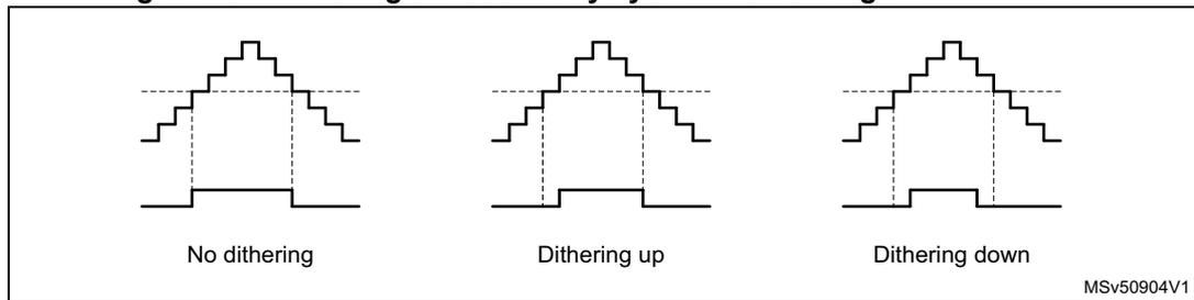
The figure displays three PWM waveforms in center-aligned mode. Each waveform consists of a series of steps representing the timer's output over eight periods. A dashed horizontal line represents the target duty cycle level. The first waveform, labeled 'No dithering', is centered exactly on the dashed line. The second waveform, labeled 'Dithering up', is shifted slightly upwards relative to the dashed line. The third waveform, labeled 'Dithering down', is shifted slightly downwards relative to the dashed line. The text 'MSv50904V1' is visible in the bottom right corner of the figure area.
Table 412 shows how the dithering pattern is added in center-aligned PWM mode.
Table 412. CCR register change dithering pattern in center-aligned PWM mode
| LSB value | PWM period | |||||||||||||||
|---|---|---|---|---|---|---|---|---|---|---|---|---|---|---|---|---|
| 1 | 2 | 3 | 4 | 5 | 6 | 7 | 8 | |||||||||
| Up | Dn | Up | Dn | Up | Dn | Up | Dn | Up | Dn | Up | Dn | Up | Dn | Up | Dn | |
| 0000 | - | - | - | - | - | - | - | - | - | - | - | - | - | - | - | - |
| 0001 | +1 | - | - | - | - | - | - | - | - | - | - | - | - | - | - | - |
| 0010 | +1 | - | - | - | - | - | - | - | +1 | - | - | - | - | - | - | - |
| 0011 | +1 | - | - | - | +1 | - | - | - | +1 | - | - | - | - | - | - | - |
| 0100 | +1 | - | - | - | +1 | - | - | - | +1 | - | - | - | +1 | - | - | - |
| 0101 | +1 | - | +1 | - | +1 | - | - | - | +1 | - | - | - | +1 | - | - | - |
| 0110 | +1 | - | +1 | - | +1 | - | - | - | +1 | - | +1 | - | +1 | - | - | - |
| 0111 | +1 | - | +1 | - | +1 | - | +1 | - | +1 | - | +1 | - | +1 | - | - | - |
| 1000 | +1 | - | +1 | - | +1 | - | +1 | - | +1 | - | +1 | - | +1 | - | +1 | - |
| 1001 | +1 | +1 | +1 | - | +1 | - | +1 | - | +1 | - | +1 | - | +1 | - | +1 | - |
| 1010 | +1 | +1 | +1 | - | +1 | - | +1 | - | +1 | +1 | +1 | - | +1 | - | +1 | - |
| 1011 | +1 | +1 | +1 | - | +1 | +1 | +1 | - | +1 | +1 | +1 | - | +1 | - | +1 | - |
| 1100 | +1 | +1 | +1 | - | +1 | +1 | +1 | - | +1 | +1 | +1 | - | +1 | +1 | +1 | - |
| 1101 | +1 | +1 | +1 | +1 | +1 | +1 | +1 | - | +1 | +1 | +1 | - | +1 | +1 | +1 | - |
| 1110 | +1 | +1 | +1 | +1 | +1 | +1 | +1 | - | +1 | +1 | +1 | +1 | +1 | +1 | +1 | - |
| 1111 | +1 | +1 | +1 | +1 | +1 | +1 | +1 | +1 | +1 | +1 | +1 | +1 | +1 | +1 | +1 | - |
38.4.12 Asymmetric PWM mode
Asymmetric mode allows two center-aligned PWM signals to be generated with a programmable phase shift. While the frequency is determined by the value of the TIMx_ARR register, the duty cycle and the phase-shift are determined by a pair of TIMx_CCRx registers. One register controls the PWM during up-counting, the second during down-counting, so that PWM is adjusted every half PWM cycle:
- • tim_oc1refc (or tim_oc2refc) is controlled by TIMx_CCR1 and TIMx_CCR2.
- • tim_oc3refc (or tim_oc4refc) is controlled by TIMx_CCR3 and TIMx_CCR4.
Asymmetric PWM mode can be selected independently on two channels (one tim_ocx output per pair of CCR registers) by writing 1110 (Asymmetric PWM mode 1) or 1111 (Asymmetric PWM mode 2) in the OCxM bits in the TIMx_CCMRx register.
Note: The OCxM[3:0] bitfield is split into two parts for compatibility reasons, the most significant bit is not contiguous with the three least significant ones.
When a given channel is used as asymmetric PWM channel, its secondary channel can also be used. For instance, if an tim_oc1refc signal is generated on channel 1 (Asymmetric PWM mode 1), it is possible to output either the tim_oc2ref signal on channel 2, or an tim_oc2refc signal resulting from asymmetric PWM mode 2.
Figure 485 shows an example of signals that can be generated using asymmetric PWM mode (channels 1 to 4 are configured in asymmetric PWM mode 2).
Figure 485. Generation of two phase-shifted PWM signals with 50% duty cycle
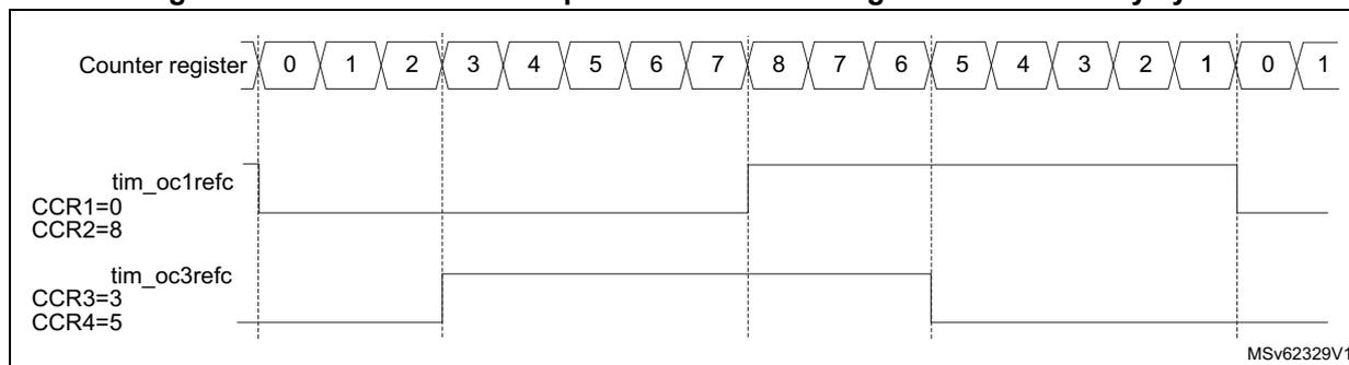
Counter register: 0 1 2 3 4 5 6 7 8 7 6 5 4 3 2 1 0 1
tim_oc1refc
CCR1=0
CCR2=8
tim_oc3refc
CCR3=3
CCR4=5
MSV62329V1
38.4.13 Combined PWM mode
Combined PWM mode allows two edge or center-aligned PWM signals to be generated with programmable delay and phase shift between respective pulses. While the frequency is determined by the value of the TIMx_ARR register, the duty cycle and delay are determined by the two TIMx_CCRx registers. The resulting signals, tim_ocxrefc, are made of an OR or AND logical combination of two reference PWMs:
- • tim_oc1refc (or tim_oc2refc) is controlled by TIMx_CCR1 and TIMx_CCR2
- • tim_oc3refc (or tim_oc4refc) is controlled by TIMx_CCR3 and TIMx_CCR4
Combined PWM mode can be selected independently on two channels (one tim_ocx output per pair of CCR registers) by writing 1100 (Combined PWM mode 1) or 1101 (Combined PWM mode 2) in the OCxM bits in the TIMx_CCMRx register.
When a given channel is used as combined PWM channel, its secondary channel must be configured in the opposite PWM mode (for instance, one in Combined PWM mode 1 and the other in Combined PWM mode 2).
Note: The OCxM[3:0] bitfield is split into two parts for compatibility reasons, the most significant bit is not contiguous with the three least significant ones.
Figure 486 shows an example of signals that can be generated using combined PWM mode, obtained with the following configuration:
- • Channel 1 is configured in Combined PWM mode 1.
- • Channel 2 is configured in PWM mode 2.
- • Channel 3 is configured in Combined PWM mode 2.
- • Channel 4 is configured in PWM mode 1.
Figure 486. Combined PWM mode on channels 1 and 3
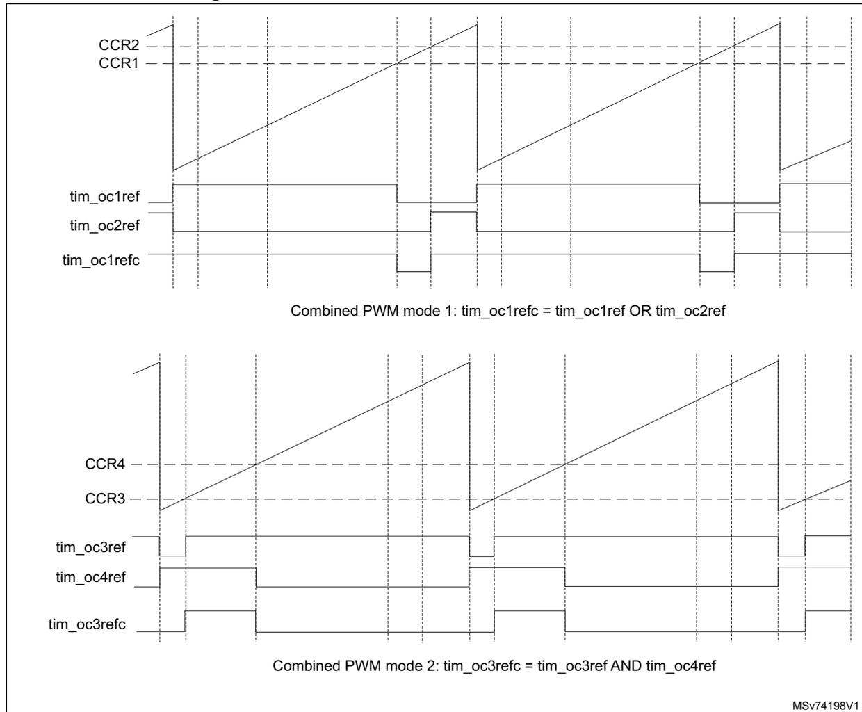
Combined PWM mode 1: \( tim\_oc1refc = tim\_oc1ref \text{ OR } tim\_oc2ref \)
Combined PWM mode 2: \( tim\_oc3refc = tim\_oc3ref \text{ AND } tim\_oc4ref \)
MSV74198V1
38.4.14 Clearing the \( tim\_ocxref \) signal on an external event
The \( tim\_ocxref \) signal of a given channel can be cleared when a high level is applied on the \( tim\_ocref\_clr\_int \) input (OCxCE enable bit in the corresponding TIMx_CCMRx register set to 1). \( tim\_ocxref \) remains low until the next transition to the active state, on the following PWM cycle. This function can only be used in Output compare and PWM modes. It does not work in Forced mode.
The \( tim\_ocref\_clr\_int \) source depends on the OCREF clear selection feature implementation, refer to Section 38.3: TIM2/TIM3/TIM4 implementation .
If the OCREF clear selection feature is implemented, the \( tim\_ocref\_clr\_int \) can be selected between the \( tim\_ocref\_clr \) input and the \( tim\_etr \) input ( \( tim\_etr\_in \) after the filter) by configuring the OCCS bit in the TIMx_SMCR register. The \( tim\_ocref\_clr \) input can be selected among several \( tim\_ocref\_clr[7:0] \) inputs, using the OCRSEL[2:0] bitfield in the TIMx_AF2 register, as shown in Figure 487 .
Figure 487. OCREF_CLR input selection multiplexer
![Figure 487: OCREF_CLR input selection multiplexer diagram. The diagram shows two multiplexers. The first multiplexer has inputs tim_ocref_clr0 through tim_ocref_clr7 and is controlled by the TIMx_AF2 register's OCRSEL[2:0] bits. Its output is tim_ocref_clr. The second multiplexer has inputs tim_ocref_clr and tim_etrf and is controlled by the TIMx_SMCR register's OCCS bits. Its output is tim_ocref_clr_int. A label MSv62341V2 is in the bottom right corner.](/RM0487-STM32U3/799cc36643b3f86a7bc447549a118370_img.jpg)
If the OCREF clear selection feature is not implemented, the
tim_ocref_clr_int
input is directly connected to the
tim_etrf
input.
For example, the
tim_ocref_clr_int
signal can be connected to the output of a comparator to be used for current handling. In this case,
tim_etr_in
must be configured as follows:
- 1. The external trigger prescaler must be kept off: bits ETPS[1:0] in the TIMx_SMCR register are cleared to 00.
- 2. The external clock mode 2 must be disabled: bit ECE in the TIMx_SMCR register is cleared to 0.
- 3. The external trigger polarity (ETP) and the external trigger filter (ETF) can be configured according to the application's needs.
Figure 488 shows the behavior of the
tim_ocxref
signal when the
tim_etrf
input becomes high, for both values of the OCxCE enable bit. In this example, the timer TIMx is programmed in PWM mode.
Figure 488. Clearing TIMx tim_ocxref
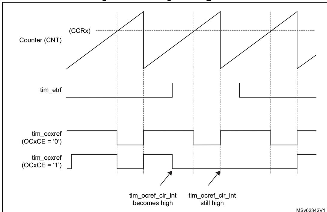
Note: In case of a PWM with a 100% duty cycle (if CCRx>ARR), tim_ocxref is enabled again at the next counter overflow.
38.4.15 One-pulse mode
One-pulse mode (OPM) is a particular case of the previous modes. It allows the counter to be started in response to a stimulus and to generate a pulse with a programmable length after a programmable delay.
Starting the counter can be controlled through the slave mode controller. Generating the waveform can be done in output compare mode or PWM mode. One-pulse mode is selected by setting the OPM bit in the TIMx_CR1 register. This makes the counter stop automatically at the next update event UEV.
A pulse can be correctly generated only if the compare value is different from the counter initial value. Before starting (when the timer is waiting for the trigger), the configuration must be:
\( CNT < CCRx \leq ARR \) (in particular, \( 0 < CCRx \) ).
Figure 489. Example of One-pulse mode
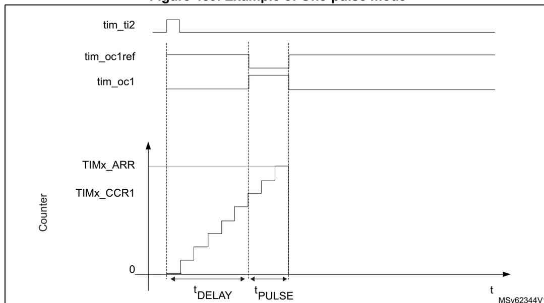
The diagram illustrates the timing for One-pulse mode. It features four horizontal signal lines at the top: tim_ti2 (trigger input), tim_oc1ref (output compare reference), tim_oc1 (output compare 1), and a Counter value graph. The tim_ti2 signal shows a single positive pulse. The tim_oc1ref signal is high when the counter is between TIMx_CCR1 and TIMx_ARR . The tim_oc1 signal is the inverse of tim_oc1ref . The Counter graph shows a staircase-like increase from 0 to TIMx_ARR . The time interval from the rising edge of tim_ti2 to the start of the counter increase is labeled t_DELAY . The duration of the counter increase (from 0 to TIMx_ARR ) is labeled t_PULSE . The diagram is labeled with MSV62344V1 in the bottom right corner.
For example if the user wants to generate a positive pulse on tim_oc1 with a length of t_PULSE and after a delay of t_DELAY as soon as a positive edge is detected on the tim_ti2 input pin.
Use tim_ti2fp2 as trigger 1:
- 1. Select the proper tim_ti2_in[15:0] source (internal or external) with the TI2SEL[3:0] bits in the TIMx_TISEL register.
- 2. Map tim_ti2fp2 on tim_ti2 by writing CC2S = 01 in the TIMx_CCMR1 register.
- 3. tim_ti2fp2 must detect a rising edge, write CC2P = 0 and CC2NP = 0 in the TIMx_CCER register.
- 4. Configure tim_ti2fp2 as trigger for the slave mode controller (tim_trgi) by writing TS = 00110 in the TIMx_SMCR register.
- 5. tim_ti2fp2 is used to start the counter by writing SMS to 110 in the TIMx_SMCR register (trigger mode).
The OPM waveform is defined by writing the compare registers (taking into account the clock frequency and the counter prescaler).
- • The \( t_{\text{DELAY}} \) is defined by the value written in the TIMx_CCR1 register.
- • The \( t_{\text{PULSE}} \) is defined by the difference between the autoreload value and the compare value (TIMx_ARR - TIMx_CCR1).
- • Suppose the user wants to build a waveform with a transition from 0 to 1 when a compare match occurs and a transition from 1 to 0 when the counter reaches the autoreload value. To do this PWM mode 2 must be enabled by writing OC1M = 111 in the TIMx_CCMR1 register. Optionally the preload registers can be enabled by writing OC1PE = 1 in the TIMx_CCMR1 register and ARPE in the TIMx_CR1 register. In this case one has to write the compare value in the TIMx_CCR1 register, the autoreload value in the TIMx_ARR register, generate an update by setting the UG bit and wait for external trigger event on tim_ti2. CC1P is written to 0 in this example.
In this example, the DIR and CMS bits in the TIMx_CR1 register must be low.
Since only one pulse (Single mode) is needed, a one must be written in the OPM bit in the TIMx_CR1 register to stop the counter at the next update event (when the counter rolls over from the autoreload value back to 0). When OPM bit in the TIMx_CR1 register is set to 0, so the Repetitive mode is selected.
Particular case: tim_ocx fast enable:
In One-pulse mode, the edge detection on tim_tix input set the CEN bit which enables the counter. Then the comparison between the counter and the compare value makes the output toggle. But several clock cycles are needed for these operations and it limits the minimum delay \( t_{\text{DELAY}} \) min we can get.
If one wants to output a waveform with the minimum delay, the OCxFE bit can be set in the TIMx_CCMRx register. Then tim_ocxref (and tim_ocx) is forced in response to the stimulus, without taking in account the comparison. Its new level is the same as if a compare match had occurred. OCxFE acts only if the channel is configured in PWM1 or PWM2 mode.
38.4.16 Retriggerable one-pulse mode
This mode allows the counter to be started in response to a stimulus and to generate a pulse with a programmable length, but with the following differences with non-retriggerable one-pulse mode described in Section 38.4.15 :
- • The pulse starts as soon as the trigger occurs (no programmable delay).
- • The pulse is extended if a new trigger occurs before the previous one is completed.
The timer must be in Slave mode, with the bits SMS[3:0] = 1000 (Combined Reset + trigger mode) in the TIMx_SMCR register, and the OCxM[3:0] bits set to 1000 or 1001 for Retriggerable OPM mode 1 or 2.
If the timer is configured in Up-counting mode, the corresponding CCRx must be set to 0 (the ARR register sets the pulse length). If the timer is configured in down-counting mode CCRx must be above or equal to ARR.
Note: In Retriggerable one-pulse mode, the CCxIF flag is not significant.
The OCxM[3:0] and SMS[3:0] bitfields are split into two parts for compatibility reasons, the most significant bit is not contiguous with the three least significant ones.
This mode must not be used with center-aligned PWM modes. It is mandatory to have CMS[1:0] = 00 in TIMx_CR1.
Figure 490. Retriggerable one-pulse mode
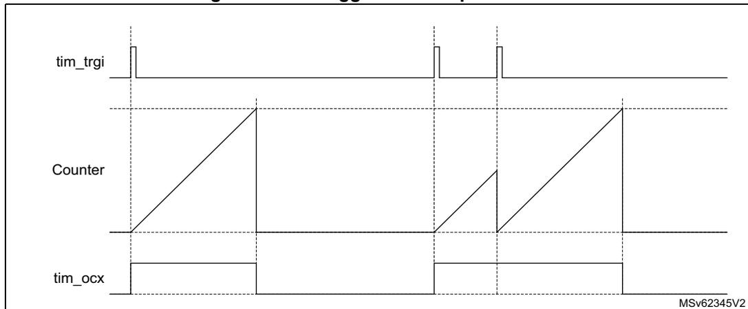
The figure is a timing diagram showing three waveforms over time. The top waveform, labeled 'tim_trgi', shows three positive pulses. The middle waveform, labeled 'Counter', shows a sawtooth-like pattern where the counter value increases linearly from a baseline until it reaches a maximum value (indicated by a horizontal dashed line), at which point it resets to the baseline. This reset occurs upon the rising edge of the first 'tim_trgi' pulse. The counter then increases again until it reaches the maximum value, at which point it resets again upon the rising edge of the second 'tim_trgi' pulse. The third 'tim_trgi' pulse occurs while the counter is still increasing from the second reset. The bottom waveform, labeled 'tim_ocx', shows a rectangular pulse. This pulse starts at the rising edge of the first 'tim_trgi' pulse and continues until the counter reaches its maximum value, at which point it drops to the baseline. The pulse is retriggered by the second 'tim_trgi' pulse, starting again and continuing until the counter reaches its maximum value a second time. The third 'tim_trgi' pulse does not retrigger the output pulse because the counter is still increasing from the previous trigger.
38.4.17 Pulse on compare mode
A pulse can be generated upon compare match event. A signal with a programmable pulse width generated when the counter value equals a given compare value, for debugging or synchronization purposes.
This mode is available for any slave mode selection, including encoder modes, in edge and center aligned counting modes. It is solely available for channel 3 and channel 4. The pulse generator is unique and is shared by the two channels, as shown on Figure 491 .
Figure 491. Pulse generator circuitry
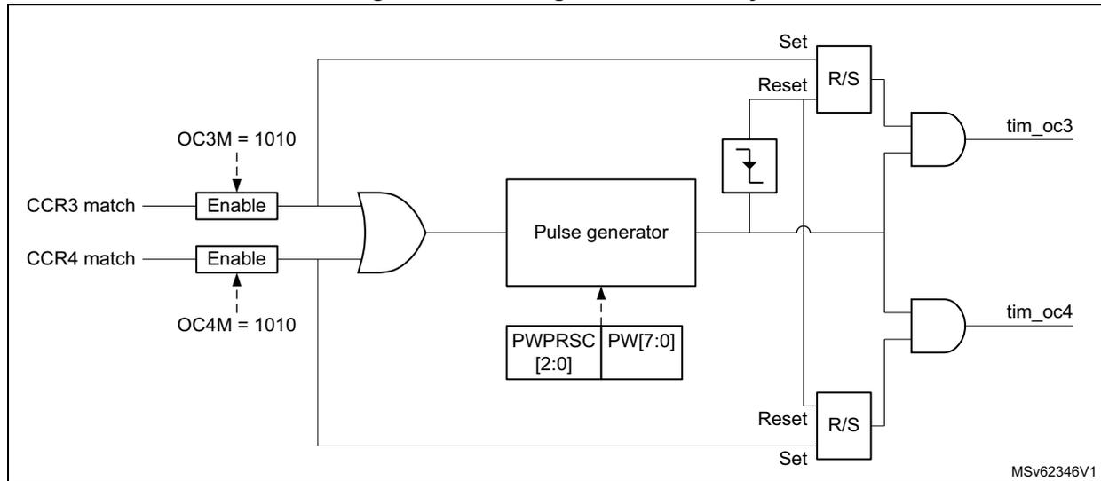
The diagram shows the logic for pulse generation. Inputs CCR3 match and CCR4 match pass through Enable blocks (controlled by OC3M = 1010 and OC4M = 1010 respectively) into an OR gate. The OR gate output feeds a Pulse generator block, which is also configured by PWPRSC[2:0] and PW[7:0] . The pulse generator output goes to two R/S flip-flops. The top R/S flip-flop has Set and Reset inputs and its output is ANDed with a signal to produce tim_oc3 . The bottom R/S flip-flop similarly produces tim_oc4 . A falling edge detector is shown between the pulse generator and the top R/S flip-flop's reset. Diagram reference: MSv62346V1.
Figure 492 shows how the pulse is generated for edge-aligned and encoder operating modes.
Figure 492. Pulse generation on compare event, for edge-aligned and encoder modes
The figure contains two timing diagrams. The top diagram shows a sawtooth Counter waveform. When the counter matches CMP3 , a trigger is generated. The tim_ocx signal goes high on a trigger. One pulse is shown as having an "Extended pulsewidth due to re-trigger" because a second trigger occurs before the first pulse finishes. The bottom diagram shows a triangular (up/down) Counter waveform. Triggers are generated on matches with CMP3 during both up-counting and down-counting, resulting in tim_ocx pulses. Diagram reference: MSv62347V1.
This output compare mode is selected using the OC3M[3:0] and OC4M[3:0] bitfields in TIMx_CCMR2 register.
The pulse width is programmed using the PW[7:0] bitfield in the register, using a specific clock prescaled according to PWPRSC[2:0] bits, as follows:
gives the resolution and maximum values depending on the prescaler value.
The pulse is retriggerable: a new trigger while the pulse is ongoing, causes the pulse to be extended.
Note: If the two channels are enabled simultaneously, the pulses are issued independently as long as the trigger on one channel is not overlapping the pulse generated on the concurrent output. On the opposite, if the two triggers are overlapping, the pulse width related to the first arriving trigger is extended (because of the retrigger), while the pulse width of the last arriving trigger is correct (as shown on Figure 493).
Figure 493. Extended pulse width in case of concurrent triggers
38.4.18 Encoder interface mode
Quadrature encoder
To select Encoder interface mode write SMS = 0001 in the TIMx_SMCR register if the counter is counting on tim_ti1 edges only, SMS = 0010 if it is counting on tim_ti2 edges only and SMS = 0011 if it is counting on both tim_ti1 and tim_ti2 edges.
Select the tim_ti1 and tim_ti2 polarity by programming the CC1P and CC2P bits in the TIMx_CCER register. CC1NP and CC2NP must be kept cleared. When needed, the input filter can be programmed as well.
The two inputs tim_ti1 and tim_ti2 are used to interface to an incremental encoder. Refer to Table 413. The counter is clocked by each valid transition on tim_ti1fp1 or tim_ti2fp2 (tim_ti1 and tim_ti2 after input filter and polarity selection, tim_ti1fp1 = tim_ti1 if not filtered and not inverted, tim_ti2fp2 = tim_ti2 if not filtered and not inverted) assuming that it is enabled (CEN bit in TIMx_CR1 register written to 1). The sequence of transitions of the two inputs is evaluated and generates count pulses as well as the direction signal. Depending on the sequence the counter counts up or down, the DIR bit in the TIMx_CR1 register is modified by hardware accordingly. The DIR bit is calculated at each transition on any input (tim_ti1 or
tim_ti2), whatever the counter is counting on tim_ti1 only, tim_ti2 only or both tim_ti1 and tim_ti2.
Encoder interface mode acts simply as an external clock with direction selection. This means that the counter just counts continuously between 0 and the autoreload value in the TIMx_ARR register (0 to ARR or ARR down to 0 depending on the direction). So the TIMx_ARR must be configured before starting. In the same way, the capture, compare, prescaler, trigger output features continue to work as normal. Encoder mode and External clock mode 2 are not compatible and must not be selected together.
In this mode, the counter is modified automatically following the speed and the direction of the quadrature encoder and its content, therefore, always represents the encoder's position. The count direction corresponds to the rotation direction of the connected sensor. The table summarizes the possible combinations, assuming tim_ti1 and tim_ti2 do not switch at the same time.
Table 413. Counting direction versus encoder signals(CC1P = CC2P = 0)
| Active edge | SMS[3:0] | Level on opposite signal (tim_ti1fp1 for tim_ti2, tim_ti2fp2 for tim_ti1) | tim_ti1fp1 signal | tim_ti2fp2 signal | ||
|---|---|---|---|---|---|---|
| Rising | Falling | Rising | Falling | |||
| Counting on tim_ti1 only x1 mode | 1110 | High | Down | Up | No count | No count |
| Low | No count | No count | No count | No count | ||
| Counting on tim_ti2 only x1 mode | 1111 | High | No count | No count | Up | Down |
| Low | No count | No count | No count | No count | ||
| Counting on tim_ti1 only x2 mode | 0001 | High | Down | Up | No count | No count |
| Low | Up | Down | No count | Down | ||
| Counting on tim_ti2 only x2 mode | 0010 | High | No count | No count | Up | Down |
| Low | No count | No count | Down | Up | ||
| Counting on tim_ti1 and tim_ti2 x4 mode | 0011 | High | Down | Up | Up | Down |
| Low | Up | Down | Down | Up | ||
A quadrature encoder can be connected directly to the MCU without external interface logic. However, comparators are normally used to convert the encoder's differential outputs to digital signals. This greatly increases noise immunity. The third encoder output which indicates the mechanical zero position, can be connected to the external trigger input and trigger a counter reset.
Figure 494 gives an example of counter operation, showing count signal generation and direction control. It also shows how input jitter is compensated where both edges are
selected. This might occur if the sensor is positioned near to one of the switching points. For this example we assume that the configuration is the following:
- • CC1S = 01 (TIMx_CCMR1 register, tim_ti1fp1 mapped on tim_ti1).
- • CC2S = 01 (TIMx_CCMR1 register, tim_ti2fp2 mapped on tim_ti2).
- • CC1P and CC1NP = 0 (TIMx_CCER register, tim_ti1fp1 noninverted, tim_ti1fp1 = tim_ti1).
- • CC2P and CC2NP = 0 (TIMx_CCER register, tim_ti2fp2 noninverted, tim_ti2fp2 = tim_ti2).
- • SMS = 0011 (TIMx_SMCR register, both inputs are active on both rising and falling edges).
- • CEN = 1 (TIMx_CR1 register, counter is enabled).
Figure 494. Example of counter operation in encoder interface mode
This timing diagram illustrates the operation of a counter in encoder interface mode. It shows three signal traces: tim_ti1 , tim_ti2 , and Counter . The diagram is divided into five phases: forward , jitter , backward , jitter , and forward . In the first forward phase, the counter increments, labeled up . In the jitter phase, the counter value fluctuates. In the backward phase, the counter decrements, labeled down . In the second jitter phase, the counter fluctuates again. In the final forward phase, the counter increments once more, labeled up . The source code MSv62349V1 is noted in the bottom right corner.
Figure 495 gives an example of counter behavior when tim_ti1fp1 polarity is inverted (same configuration as above except CC1P = 1).
Figure 495. Example of encoder interface mode with tim_ti1fp1 polarity inverted
This timing diagram shows the counter operation when the tim_ti1fp1 polarity is inverted. The signal traces for tim_ti1 , tim_ti2 , and Counter are shown across the same five phases: forward , jitter , backward , jitter , and forward . However, the counter's behavior is reversed compared to Figure 494. In the first forward phase, the counter now decrements, labeled down . In the backward phase, it increments, labeled up . In the final forward phase, it decrements again, labeled down . The source code MSv62350V1 is noted in the bottom right corner.
Figure 496 shows the timer counter value during a speed reversal, for various counting modes.
Figure 496. Quadrature encoder counting modes
The figure is a timing diagram illustrating quadrature encoder counting modes during a speed reversal. It consists of four horizontal waveforms:
- tim_ti1 : A square wave representing the first quadrature signal.
- tim_ti2 : A square wave representing the second quadrature signal, phase-shifted relative to tim_ti1.
- DIR bit : A logic signal that indicates the direction of rotation. It is high for clockwise rotation and low for counter-clockwise rotation.
- Counter x4 : A counter that increments or decrements by 4 for each full cycle of the quadrature signals. The sequence shown is: 6, 7, 8, 9, 0, 1, 2, 3, 4, 5, 4, 3, 2, 1, 0, 9, 8, 7, 6, 5, 4, 3, 2.
- Counter x2 : A counter that increments or decrements by 2 for each full cycle. The sequence shown is: 8, 9, 0, 1, 2, 1, 0, 9, 8, 7, 6.
- Counter x1 : A counter that increments or decrements by 1 for each full cycle. The sequence shown is: 9, 0, 1, 0, 9, 8.
The diagram shows a speed reversal where the direction of rotation changes. The DIR bit transitions from high to low at the start of the reversal. The counter values reflect this change, with the sequence of numbers reversing (e.g., from 5 down to 4 in Counter x4). The source identifier MSV62351V1 is visible in the bottom right corner.
The timer, when configured in Encoder Interface mode provides information on the sensor's current position. Dynamic information can be obtained (speed, acceleration, deceleration) by measuring the period between two encoder events using a second timer configured in capture mode. The output of the encoder which indicates the mechanical zero can be used for this purpose. Depending on the time between two events, the counter can also be read at regular times. This can be done by latching the counter value into a third input capture register if available (then the capture signal must be periodic and can be generated by another timer). When available, it is also possible to read its value through a DMA request.
The IUFREMAP bit in the TIMx_CR1 register forces a continuous copy of the update interrupt flag (UIF) into the timer counter register's bit 31 (TIMx_CNT[31]). This allows both the counter value and a potential roll-over condition signaled by the UIFCPY flag to be read in an atomic way. It eases the calculation of angular speed by avoiding race conditions caused, for instance, by a processing shared between a background task (counter reading) and an interrupt (update interrupt).
There is no latency between the UIF and UIFCPY flag assertions.
In 32-bit timer implementations, when the IUFREMAP bit is set, bit 31 of the counter is overwritten by the UIFCPY flag upon read access (the counter's most significant bit is only accessible in write mode).
Clock plus direction encoder mode
In addition to the quadrature encoder mode, the timer offers support for other types of encoders.
In the "clock plus direction" mode shown on Figure 497, the clock is provided on a single line, on tim_ti2, while the direction is forced using the tim_ti1 input.
This mode is enabled with the SMS[3:0] bitfield in the TIMx_SMCR register, as following:
- • 1010: x2 mode, the counter is updated on both rising and falling edges of the clock.
- • 1011: x1 mode, the counter is updated on a single clock edge, as per CC2P bit value: CC2P = 0 corresponds to rising edge sensitivity and CC2P = 1 corresponds to falling edge sensitivity.
The polarity of the direction signal on tim_ti1 is set with the CC1P bit: 0 corresponds to positive polarity (up-counting when tim_ti1 is high and down-counting when tim_ti1 is low) and CC1P = 1 corresponds to negative polarity (up-counting when tim_ti1 is low and down-counting when tim_ti1 is high).
Figure 497. Direction plus clock encoder mode
The diagram illustrates the counter behavior based on the direction signal (tim_ti1) and clock signal (tim_ti2):
- tim_ti1: Acts as a direction control. It is high for the first half and low for the second half.
- tim_ti2: A square wave clock signal.
- Counter x2 mode:
Updates on every edge of tim_ti2.
- While tim_ti1 is high: 6 → 7 → 8 → 9 → 10 → 11
- While tim_ti1 is low: 11 → 10 → 9 → 8 → 7 → 6
- Counter x1 mode:
Updates only on rising edges of tim_ti2.
- While tim_ti1 is high: 6 → 7 → 8 → 9
- While tim_ti1 is low: 9 → 8 → 7
MSv62352V1
Directional clock encoder mode
In the “directional clock” mode on Figure 498 , the clocks are provided on two lines, with a single one at once, depending on the direction, so as to have one up-counting clock line and one down-counting clock line.
This mode is enabled with the SMS[3:0] bitfield in the TIMx_SMCR register, as following:
- • 1100: x2 mode, the counter is updated on both rising and falling edges of any of the two clock lines. The CC1P and CC2P bits are coding for the clock idle state. CCxP = 0 corresponds to high-level idle state (refer to Figure 498 ) and CCxP = 1 corresponds to low-level idle state (refer to Figure 499 ).
- • 1101: x1 mode, the counter is updated on a single clock edge, as per CC1P and CC2P bit value. CCxP = 0 corresponds to falling edge sensitivity and high-level idle state (refer to Figure 498 ), CCxP = 1 corresponds to rising edge sensitivity and low-level idle state (refer to Figure 499 ).
Figure 498. Directional clock encoder mode (CC1P = CC2P = 0)
Timing diagram for Figure 498. The diagram shows five horizontal timelines. The first timeline, tim_ti1 , starts high and has three falling edges. The second timeline, tim_ti2 , starts low and has three rising edges. The third timeline, DIR bit , is initially low and transitions to high at the first falling edge of tim_ti1 . The fourth timeline, Counter x2 mode , shows a sequence of counter values: 6, 7, 8, 9, 10, 11, 10, 9, 8, 7, 6, 5. The fifth timeline, Counter x1 mode , shows a sequence of counter values: 6, 7, 8, 7, 6, 5. Vertical dashed lines indicate the timing of the counter updates relative to the timer input edges. The identifier MSv62353V1 is in the bottom right corner.
Figure 499. Directional clock encoder mode (CC1P = CC2P = 1)
Timing diagram for Figure 499. The diagram shows five horizontal timelines. The first timeline, tim_ti1 , starts low and has three rising edges. The second timeline, tim_ti2 , starts high and has three falling edges. The third timeline, DIR bit , is initially low and transitions to high at the first rising edge of tim_ti1 . The fourth timeline, Counter x2 mode , shows a sequence of counter values: 6, 7, 8, 9, 10, 11, 10, 9, 8, 7, 6, 5. The fifth timeline, Counter x1 mode , shows a sequence of counter values: 7, 8, 9, 8, 7, 6. Vertical dashed lines indicate the timing of the counter updates relative to the timer input edges. The identifier MSv62354V1 is in the bottom right corner.
Table 414 details how the directional clock mode operates, for any input transition.
Table 414. Counting direction versus encoder signals and polarity settings
| Directional clock mode | SMS[3:0] | Level on opposite signal (tim_ti1fp1 for tim_ti2, tim_ti2fp2 for tim_ti1) | tim_ti1fp1 signal | tim_ti2fp2 signal | ||
|---|---|---|---|---|---|---|
| Rising | Falling | Rising | Falling | |||
| x2 mode CCxP = 0 | 1100 | High | Down | Down | Up | Up |
| Low | No count | No count | No count | No count | ||
| x2 mode CCxP = 1 | 1100 | High | No count | No count | No count | No count |
| Low | Down | Down | Up | Up | ||
| x1 mode CCxP = 0 | 1101 | High | No count | Down | No count | Up |
| Low | No count | No count | No count | No count | ||
| x1 mode CCxP = 1 | 1101 | High | No count | No count | No count | No count |
| Low | Down | No count | Up | No count | ||
Index input
The counter can be reset by an index signal coming from the encoder, indicating an absolute reference position. The index signal must be connected to the tim_etr_in input. It can be filtered using the digital input filter.
The index functionality is enabled with the IE bit in the TIMx_ECR register. The IE bit must be set only in encoder mode, when the SMS[3:0] bitfield has the following values: 0001, 0010, 011, 1010, 1011, 1100, 1101, 1110, 1111.
Available encoders are proposed with several options for index pulse conditioning, as per Figure 500:
- • Gated with A and B: the pulse width is 1/4 of one channel period, aligned with both A and B edges.
- • Gated with A (or gated with B): the pulse width is 1/2 of one channel period, aligned with the two edges on channel A (resp. channel B).
- • Ungated: the pulse width is up to one channel period, without any alignment to the edges.
Figure 500. Index gating options
The circuitry tolerates jitter on index signal, whatever the gating mode, as shown on Figure 501 .
In ungated mode, the signal must be strictly below two encoder periods. If the pulse width is greater or equal to two encoder period, the counter is reset multiple times.
Figure 501. Jittered Index signals
The timer supports the three gating options identically, without any specific programming needed. It is only necessary to define on which encoder state (for example channel A and channel B state combination) the index must be synchronized, using the IPOS[1:0] bitfield in the TIMx_ECR register.
The index detection event acts differently depending on counting direction to ensure symmetrical operation during speed reversal:
- • The counter is reset during up-counting (DIR bit = 0).
- • The counter is set to TIMx_ARR when down-counting.
This allows the index to be generated on the very same mechanical angular position whatever the counting direction. Figure 502 shows at which position is the index generated, for a simplistic example (an encoder providing four edges par mechanical rotation).
Figure 502. Index generation for IPOS[1:0] = 11
    graph TD
    S1("AB = 00
State 1") -- "Rotor angle = 0°" --> S2("AB = 01
State 2")
    S2 -- "Rotor angle = 90°" --> S3("AB = 11
State 3")
    S3 -- "Rotor angle = 180°" --> S4("AB = 10
State 4")
    S4 -- "Rotor angle = 270°" --> S1
    S1 -- "Down-counting" --> S4
    S4 -- "Down-counting" --> S3
    S3 -- "Down-counting" --> S2
    S2 -- "Down-counting" --> S1
    subgraph Counting_Direction
    Up["Up-counting"]
    Down["Down-counting"]
    end
The diagram shows four states in a circular transition: State 1 (AB=00), State 2 (AB=01), State 3 (AB=11), and State 4 (AB=10). Transitions are marked with rotor angles: 0°, 90°, 180°, and 270°. An arrow points to the transition between State 4 and State 1 with the text: "The index event is always generated here". MSv45767V1
Figure 503 presents waveforms and corresponding values for IPOS[1:0] = 11. It shows that the instant at which the counter value is forced is automatically adjusted depending on the counting direction:
- • Counter set to 0 when encoder state is 11 (ChA = 1, ChB = 1), when up-counting (DIR bit = 0).
- • Counter set to TIMx_ARR when exiting the 11 state, when down-counting (DIR bit = 1).
An interrupt can be issued upon index detection event.
The arrows are indicating on which transition is the index event interrupt generated.
Figure 503. Counter reading with index gated on channel A (IPOS[1:0] = 11)
The timing diagram illustrates the relationship between Channel A, Channel B, Index signal, DIR bit, and the Counter value.
Counter sequence: 5, 6, 7, 0, 1, 2, 3, 4, 5, 6 (DIR bit transitions from 0 to 1), 5, 4, 3, 2, 1, 0, 7, 6, 5, 4, 3, 2, 1.
Arrows indicate index events: one occurs when the counter resets to 0 (up-counting) and another when it resets to 7 (down-counting). MSv45768V1
Figure 504 presents waveforms and corresponding values for the ungated mode. The arrows are indicating on which transition is the index event generated.
Figure 504. Counter reading with index ungated (IPOS[1:0] = 00)
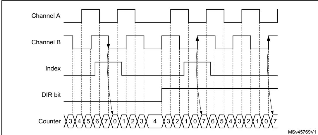
This timing diagram illustrates the counter reading with the index signal ungated (IPOS[1:0] = 00). It shows five signal traces over time: Channel A, Channel B, Index, DIR bit, and Counter. Channel A and B are square waves representing encoder signals. The Index signal is a pulse that goes high when both Channel A and B are high. The DIR bit indicates the direction of rotation. The Counter shows the current count value. Arrows point to the rising edges of the Index signal that correspond to counter updates. The counter sequence shown is 3, 4, 5, 6, 7, 0, 1, 2, 3, 4, 3, 2, 1, 0, 7, 6, 5, 4, 3, 2, 1, 0, 7. The diagram is labeled MSv45769V1.
Figure 505 shows how the gated on A & B mode is handled, for various pulse alignment scenarios. The arrows are indicating on which transition is the index event generated.
Figure 505. Counter reading with index gated on channel A and B
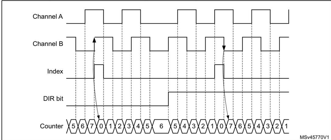
This timing diagram illustrates the counter reading with the index signal gated on Channel A and B. It shows five signal traces over time: Channel A, Channel B, Index, DIR bit, and Counter. The Index signal is generated only when both Channel A and B are high. The DIR bit indicates the direction of rotation. The Counter shows the current count value. Arrows point to the rising edges of the Index signal that correspond to counter updates. The counter sequence shown is 5, 6, 7, 0, 1, 2, 3, 4, 5, 6, 5, 4, 3, 2, 1, 0, 7, 6, 5, 4, 3, 2, 1. The diagram is labeled MSv45770V1.
Figure 506 and Figure 507 detail the case where the subsequent index pulse may be narrower than one quarter of the encoder clock period.
Figure 506. Encoder mode behavior in case of narrow index pulse (IPOS[1:0] = 11)
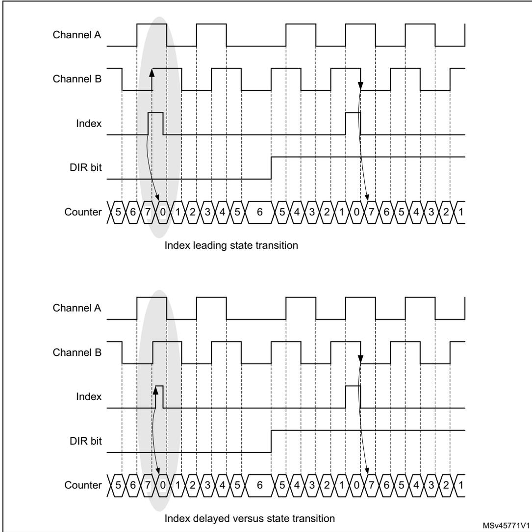
The figure consists of two timing diagrams illustrating encoder mode behavior with a narrow index pulse (IPOS[1:0] = 11).
Top Diagram: Index leading state transition
- Channel A: A square wave signal.
- Channel B: A square wave signal, phase-shifted relative to Channel A.
- Index: A narrow pulse. The counter resets to 0 on its rising edge.
- DIR bit: A signal that changes state from low to high halfway through the sequence.
- Counter: A sequence of values: 5, 6, 7, 0, 1, 2, 3, 4, 5, 6, 5, 4, 3, 2, 1, 0, 7, 6, 5, 4, 3, 2, 1. The reset to 0 occurs at the rising edge of the Index pulse.
Index leading state transition
Bottom Diagram: Index delayed versus state transition
- Channel A: A square wave signal.
- Channel B: A square wave signal, phase-shifted relative to Channel A.
- Index: A narrow pulse. The counter resets to 0 on its falling edge.
- DIR bit: A signal that changes state from low to high halfway through the sequence.
- Counter: A sequence of values: 5, 6, 7, 0, 1, 2, 3, 4, 5, 6, 5, 4, 3, 2, 1, 0, 7, 6, 5, 4, 3, 2, 1. The reset to 0 occurs at the falling edge of the Index pulse.
Index delayed versus state transition
MSv45771V1
Figure 507. Counter reset Narrow index pulse (closer view, ARR = 0x07)
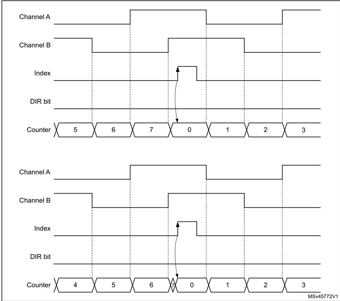
The figure illustrates the timing for a counter reset triggered by a narrow index pulse. It consists of two vertically stacked timing diagrams. Both diagrams show five signals over time: Channel A, Channel B, Index, DIR bit, and Counter. In the top diagram, the Counter sequence is 5, 6, 7, 0, 1, 2, 3. A narrow positive pulse on the Index line occurs at the same time as a falling edge of Channel B. This event causes the Counter to reset from 7 to 0. An arrow points from the rising edge of the Index pulse to the Counter reset. In the bottom diagram, the Counter sequence is 4, 5, 6, 0, 1, 2, 3. Similarly, a narrow positive pulse on the Index line coincides with a falling edge of Channel B, causing the Counter to reset from 6 to 0. An arrow points from the rising edge of the Index pulse to the Counter reset. The DIR bit is shown as a constant low level in both diagrams. The text 'MSV45772V1' is located in the bottom right corner of the figure.
Figure 508 shows how the index is managed in x1 and x2 modes.
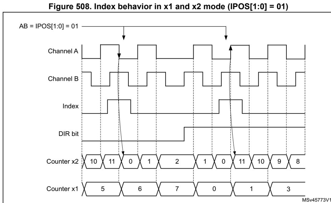
Figure 508. Index behavior in x1 and x2 mode (IPOS[1:0] = 01)
AB = IPOS[1:0] = 01
Channel A
Channel B
Index
DIR bit
Counter x2: 10, 11, 0, 1, 2, 1, 0, 11, 10, 9, 8
Counter x1: 5, 6, 7, 0, 1, 3
MSv45773V1
Directional index sensitivity
The IDIR[1:0] bitfield in the TIMx_ECR register allows the index to be active only in a selected counting direction.
Figure 509 shows the relationship between index and counter reset events, depending on IDIR[1:0] value.
![Timing diagram showing DIR bit, Counter, Index input, and Counter reset for IDIR[1:0] values 00, 01, and 10. The diagram is split into UP-counting and Down-counting sections. Counter reset pulses are shown for each IDIR setting, indicating when the index input is active.](/RM0487-STM32U3/08c325e42123d8f37d2354767862ff98_img.jpg)
Figure 509. Directional index sensitivity
DIR bit: UP-counting, Down-counting
Counter
Index input
Counter reset
IDIR[1:0]=00
IDIR[1:0]=01
IDIR[1:0]=10
MSv45774V1
Special first index event management
The FIDX bit in the TIMx_ECR register allows the index to be taken only once, as shown on Figure 510 . Once the first index has arrived, any subsequent index is ignored. If needed, the circuitry can be rearmed by writing the FIDX bit to 0 and setting it again to 1.
Figure 510. Counter reset as function of FIDX bit setting
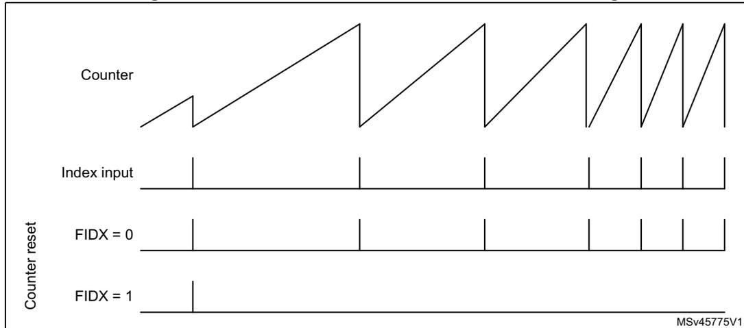
Timing diagram illustrating the counter reset behavior based on the FIDX bit setting. The diagram shows four waveforms over time:
- Counter: A sawtooth waveform representing the counter value. It increases linearly and resets to zero upon a valid index event.
- Index input: A series of pulses. The first pulse occurs while FIDX = 0. Subsequent pulses occur while FIDX = 1. Only the first pulse causes a counter reset.
- Counter reset (FIDX = 0): A pulse that goes high when the first index input pulse occurs, causing the counter to reset.
- Counter reset (FIDX = 1): A pulse that goes high only for the first index input pulse. Subsequent index input pulses do not cause a reset because the FIDX bit has been cleared by the first reset event.
MSv45775V1
Index blanking
The index event can be blanked using the tim_ti3 or tim_ti4 inputs. During the blanking window, the index events are no longer resetting the counter, as shown on Figure 511 .
This mode is enabled using the IBLK[1:0] bitfield in the TIMx_ECR register, as following:
- • IBLK[1:0] = 00: Index signal always active.
- • IBLK[1:0] = 01: Index signal blanking on tim_ti3 input.
- • IBLK[1:0] = 10: Index signal blanking on tim_ti4 input.
Figure 511. Index blanking
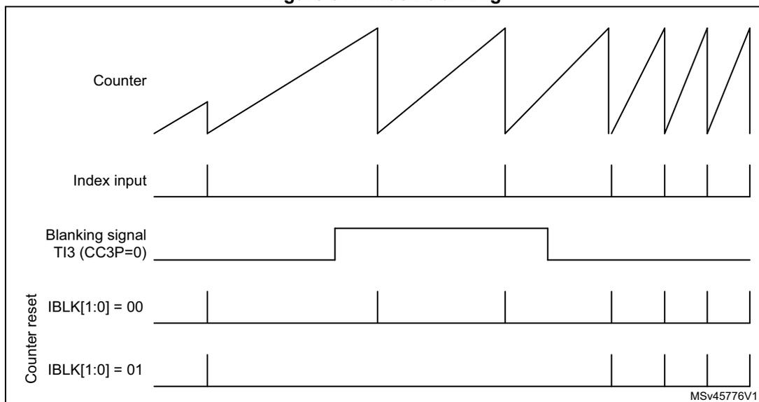
Timing diagram illustrating the index blanking behavior. The diagram shows five waveforms over time:
- Counter: A sawtooth waveform representing the counter value. It increases linearly and resets to zero upon a valid index event.
- Index input: A series of pulses. The first pulse occurs while the blanking signal is low. Subsequent pulses occur while the blanking signal is high. Only the first pulse causes a counter reset.
- Blanking signal TI3 (CC3P=0): A signal that goes high to enable blanking. During this high period, subsequent index input pulses are ignored by the counter.
- Counter reset (IBLK[1:0] = 00): A pulse that goes high for every index input pulse, causing the counter to reset repeatedly.
- Counter reset (IBLK[1:0] = 01): A pulse that goes high only for the first index input pulse. Subsequent index input pulses, which occur while the blanking signal is high, do not cause a reset.
MSv45776V1
Index management in nonquadrature mode
Figure 512 and Figure 513 detail how the index is managed in directional clock mode and clock plus direction mode, when the SMS[3:0] bitfield is equal to 1010, 1011, 1100, 1101.
For both of these modes, the index sensitivity is set with the IPOS[0] bit as following:
- • IPOS[0] = 0: Index is detected on clock low level.
- • IPOS[0] = 1: Index is detected on clock high level.
The IPOS[1] bit is not-significant.
Figure 512. Index behavior in clock + direction mode, IPOS[0] = 1
![Timing diagram for Figure 512 showing index behavior in clock + direction mode with IPOS[0] = 1. The diagram includes five waveforms: Direction (TI1), Clock (TI2), Index, Counter x2 mode, and Counter x1 mode. The Counter x2 mode sequence is 7, 0, 1, 2, 3, 4, 3, 2, 7, 6, 5. The Counter x1 mode sequence is 7, 0, 1, 2, 1, 7. Arrows indicate that the index pulse is detected on the rising edge of the clock when the direction is high.](/RM0487-STM32U3/d9276ff140944511c1b30b407e49cef0_img.jpg)
Timing diagram for Figure 512. The diagram shows the relationship between Direction (TI1), Clock (TI2), Index, Counter x2 mode, and Counter x1 mode. The Counter x2 mode sequence is 7, 0, 1, 2, 3, 4, 3, 2, 7, 6, 5. The Counter x1 mode sequence is 7, 0, 1, 2, 1, 7. Arrows indicate that the index pulse is detected on the rising edge of the clock when the direction is high.
Figure 513. Index behavior in directional clock mode, IPOS[0] = 1
![Timing diagram for Figure 513 showing index behavior in directional clock mode with IPOS[0] = 1. The diagram includes five waveforms: Clock Down (TI1), Clock Up (TI2), DIR bit, Counter x2 mode, and Counter x1 mode. The Counter x2 mode sequence is 9, 0, 1, 2, 3, 4, 3, 2, 1, 0, 9, 8. The Counter x1 mode sequence is 9, 0, 1, 2, 1, 0, 9. Arrows indicate that the index pulse is detected on the rising edge of the clock when the DIR bit is high.](/RM0487-STM32U3/a6b874d510b49ba088b2a5a34832bb6f_img.jpg)
Timing diagram for Figure 513. The diagram shows the relationship between Clock Down (TI1), Clock Up (TI2), DIR bit, Counter x2 mode, and Counter x1 mode. The Counter x2 mode sequence is 9, 0, 1, 2, 3, 4, 3, 2, 1, 0, 9, 8. The Counter x1 mode sequence is 9, 0, 1, 2, 1, 0, 9. Arrows indicate that the index pulse is detected on the rising edge of the clock when the DIR bit is high.
Encoder error management
For encoder configurations where two quadrature signals are available, it is possible to detect transition errors. The reading on the two inputs corresponds to a 2-bit gray code which can be represented as a state diagram, on Figure 514. A single bit is expected to change at once. An erroneous transition sets the TERRF interrupt flag in the TIMx_SR
status register. A transition error interrupt is generated if the TERRIE bit is set in the TIMx_DIER register.
Figure 514. State diagram for quadrature encoded signals
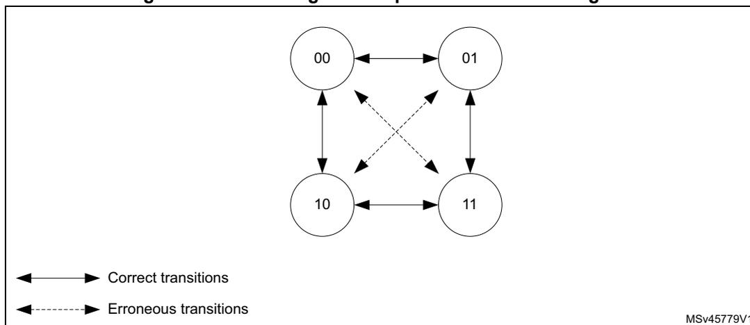
The diagram illustrates the state transitions for quadrature encoded signals. It features four circular nodes arranged in a square, labeled 00 (top-left), 01 (top-right), 10 (bottom-left), and 11 (bottom-right). Solid double-headed arrows represent correct transitions between adjacent states: 00 to 01, 01 to 11, 11 to 10, and 10 to 00. Dashed double-headed arrows represent erroneous transitions between diagonal states: 00 to 11 and 10 to 01. A legend at the bottom left shows a solid double-headed arrow labeled 'Correct transitions' and a dashed double-headed arrow labeled 'Erroneous transitions'. The identifier MSv45779V1 is located in the bottom right corner of the diagram area.
For encoder having an index signal, it is possible to detect abnormal operation resulting in an excess of pulses per revolution. An encoder with N pulses per revolution provides \( 4 \times N \) counts per revolution. The index signal resets the counter every \( 4 \times N \) clock periods.
If the counter value is incremented from TIMx_ARR to 0 or decremented from 0 to TIMx_ARR value without any index event, this is reported as an index position error.
The overflow threshold is programmed using the TIMx_ARR register. A 1000 lines encoder results in a counter value being between 0 and 3999 (in 4x reading mode). The overflow detection threshold must be programmed by setting \( \text{TIMx\_ARR} = 3999 + 1 = 4000 \) .
The error assertion is delayed to the transition 0 to 1 when in up-counting. This is to cope with narrow index pulses in gated A and B mode, as shown on Figure 515 .
Figure 515. Up-counting encoder error detection
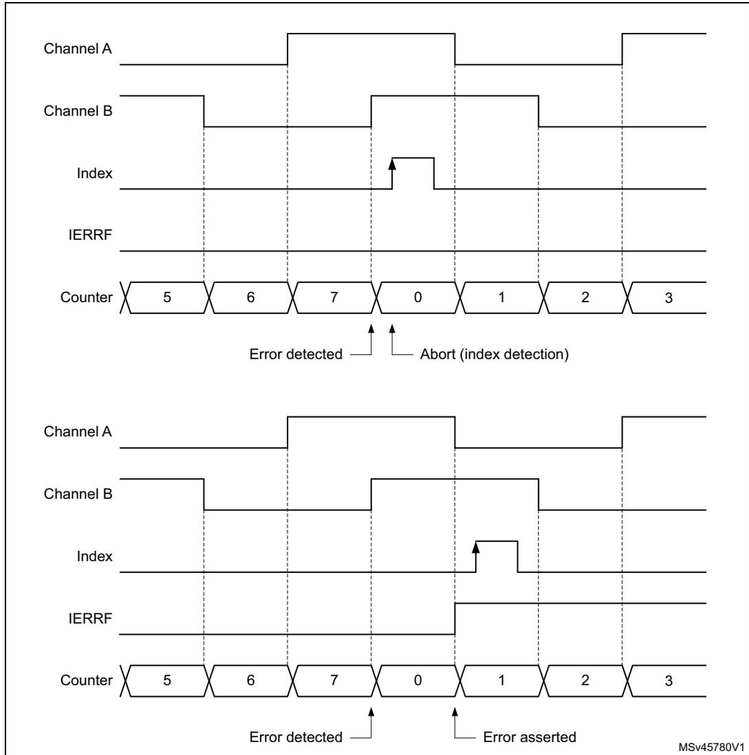
The figure illustrates two timing scenarios for up-counting encoder error detection. Both scenarios show the relationship between Channel A, Channel B, Index, IERRF, and the Counter.
Top Scenario:
- Channel A: Starts low, transitions high at the transition from counter value 6 to 7, and transitions back low at the transition from 0 to 1.
- Channel B: Starts high, transitions low at the transition from 5 to 6, and transitions back high at the transition from 7 to 0.
- Index: Shows a narrow high pulse starting at the transition from 7 to 0.
- IERRF: Remains low throughout this scenario.
- Counter: Shows values 5, 6, 7, 0, 1, 2, 3. An arrow labeled "Error detected" points to the transition from 7 to 0. Another arrow labeled "Abort (index detection)" points to the rising edge of the Index pulse at the 0 position.
Bottom Scenario:
- Channel A: Starts low, transitions high at the transition from 6 to 7, and transitions back low at the transition from 0 to 1.
- Channel B: Starts high, transitions low at the transition from 5 to 6, and transitions back high at the transition from 7 to 0.
- Index: Shows a narrow high pulse starting at the transition from 0 to 1.
- IERRF: Transitions high at the transition from 0 to 1, coinciding with the start of the Index pulse.
- Counter: Shows values 5, 6, 7, 0, 1, 2, 3. An arrow labeled "Error detected" points to the transition from 7 to 0. Another arrow labeled "Error asserted" points to the rising edge of the IERRF signal at the 1 position.
MSV45780V1
In down-counting mode, the detection is conditioned by a preliminary transition from 1 to 0. This is to cope with narrow index pulses in gated A and B mode, as shown on Figure 516 , to avoid any false error detection in case the encoder dithers between TIMx_ARR and 0 immediately after the index detection.
Figure 516. Down-counting encode error detection
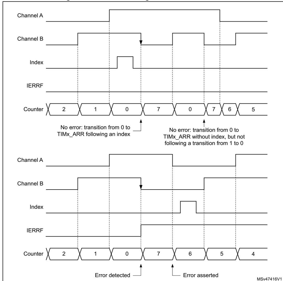
The figure illustrates two timing scenarios for down-counting encode error detection. In the top scenario, the counter reaches 0, an index pulse occurs, and then the counter transitions to 7. This is labeled 'No error: transition from 0 to TIMx_ARR following an index'. In the bottom scenario, the counter reaches 0 and immediately transitions to 7 without an index pulse. This transition triggers the IERRF flag, labeled 'Error detected' and 'Error asserted'. The text 'No error: transition from 0 to TIMx_ARR without index, but not following a transition from 1 to 0' is also present. The signals shown are Channel A, Channel B, Index, IERRF, and Counter.
An index error sets the IERRF interrupt flag in the TIMx_SR status register. An index error interrupt is generated if the IERRIE bit is set in the TIMx_DIER register.
Functional encoder interrupts
The following interrupts are also available in encoder mode
- • Direction change: any change of the counting direction in encoder mode causes the DIR bit in the TIMx_CR1 register to toggle. The direction change sets the DIRF interrupt flag in the TIMx_SR status register. A direction change interrupt is generated if the DIRIE bit is set in the TIMx_DIER register.
- • Index event: the index event sets the IDXF interrupt flag in the TIMx_SR status register. An index interrupt is generated if the IDXIE bit is set in the TIMx_DIER register.
Slave mode selection preload for run-time encoder mode update
It can be necessary to switch from one encoder mode to another during run-time. This is typically done at high-speed to decrease the update interrupt rate, by switching from x4 to x2 or x1 mode, as shown on Figure 517.
For this purpose, the SMS[3:0] bit can be preloaded. This is enabled by setting the SMSPE enable bit in the TIMx_SMCR register. The trigger for the transfer from SMS[3:0] preload to active value can be selected with the SMSPS bit in the TIMx_SMCR register.
- • SMSPS = 0: the transfer is triggered by the update event (UEV) occurring when the counter overflows when up-counting, and underflows when down-counting.
- • SMSPS = 1: the transfer is triggered by the index event.
Figure 517. Encoder mode change with preload transferred on update (SMSPS = 0)
![Timing diagram showing encoder mode change from x4 to x2 to x1 mode. The diagram illustrates the relationship between the encoder clock output, update events, preload values, and active values for the SMS[3:0] bits. The x4 mode shows a high-frequency sawtooth clock. The x2 mode shows a medium-frequency sawtooth clock. The x1 mode shows a low-frequency sawtooth clock. Update events are shown as pulses. Preload values are shown as SMS = 0011, SMS = 0001, and SMS = 1110. Active values are shown as SMS = 0011, SMS = 0001, and SMS = 1110. Arrows indicate the transfer of preload values to active values upon update events.](/RM0487-STM32U3/098038c4774d445287432c03dbd424d0_img.jpg)
The diagram illustrates the timing for an encoder mode change. The top row shows the encoder clock output, which is a sawtooth wave. It starts in x4 mode (high frequency), changes to x2 mode (medium frequency), and then to x1 mode (low frequency). The second row shows the 'Update event' signal, which is a series of pulses. The third row shows the 'Preload value' for the SMS[3:0] bits, which are set to 0011, 0001, and 1110 respectively for the x4, x2, and x1 modes. The fourth row shows the 'Active value' for the SMS[3:0] bits, which follow the preload values. Arrows indicate that the active value is updated to match the preload value upon an update event (UEV). The diagram is labeled MSv45781V1.
Encoder clock output
The encoder mode operating principle is not perfectly suited for high-resolution velocity measurements, at low speed, as it requires a relatively long integration time to have a sufficient number of clock edges and a precise measurement.
At low speed, a better solution is to do an edge-to-edge clock period measurement. This can be achieved using a slave timer. The timer can output the encoder clock information on the tim_trgo output. The slave timer can then perform a period measurement and provide velocity information for each and every encoder clock edge.
This mode is enabled by setting the MMS[3:0] bitfield to 1000, in the TIMx_CR2 register. It is valid for the following SMS[3:0] values: 0001, 0010, 0011, 1010, 1011, 1100, 1101, 1110, 1111. Any other SMS[3:0] code is not allowed and may lead to unexpected behavior.
38.4.19 Direction bit output
It is possible to output a direction signal out of the timer, on the tim_oc3 and tim_oc4 output signals (copy of the DIR bit in the TIMx_CR1 register). This is achieved by setting the OC3M[3:0] or the OC4M[3:0] bitfield to 1011 in the TIMx_CCMR2 register.
This feature can be used for monitoring the counting direction (or rotation direction) in encoder mode, or to have a signal indicating the up/down phases in center-aligned PWM mode.
38.4.20 UIF bit remapping
The IUFREMAP bit in the TIMx_CR1 register forces a continuous copy of the update interrupt flag (UIF) into bit 31 of the timer counter register's bit 31 (TIMx_CNT[31]). This is used to atomically read both the counter value and a potential roll-over condition signaled by the UIFCPY flag. It eases the calculation of angular speed by avoiding race conditions caused, for instance, by a processing shared between a background task (counter reading) and an interrupt (update interrupt).
There is no latency between the UIF and UIFCPY flag assertions.
In 32-bit timer implementations, when the IUFREMAP bit is set, bit 31 of the counter is overwritten by the UIFCPY flag upon read access (the counter's most significant bit is only accessible in write mode).
38.4.21 Timer input XOR function
The TI1S bit in the TIMx_CR2 register, allows the input filter of channel 1 to be connected to the output of an XOR gate, combining the three input pins tim_ti1, tim_ti2 and tim_ti3.
The XOR output can be used with all the timer input functions such as trigger or input capture.
An example of this feature used to interface Hall sensors is given in Section 37.3.29: Interfacing with Hall sensors .
38.4.22 Timers and external trigger synchronization
The TIMx timers can be synchronized with an external trigger in several modes: Reset mode, Gated mode, Trigger mode, Reset + trigger and gated + reset modes.
Slave mode: Reset mode
The counter and its prescaler can be reinitialized in response to an event on a trigger input. Moreover, if the URS bit from the TIMx_CR1 register is low, an update event UEV is generated. Then all the preloaded registers (TIMx_ARR, TIMx_CCRx) are updated.
In the following example, the upcounter is cleared in response to a rising edge on tim_ti1 input:
- 1. Configure the channel 1 to detect rising edges on tim_ti1. Configure the input filter duration (in this example, we do not need any filter, so we keep IC1F = 0000). The capture prescaler is not used for triggering, so it does not need to be configured. The CC1S bits select the input capture source only, CC1S = 01 in the TIMx_CCMR1 register. Write CC1P = 0 and CC1NP = 0 in TIMx_CCER register to validate the polarity (and detect rising edges only).
- 2. Configure the timer in reset mode by writing SMS = 100 in TIMx_SMCR register. Select tim_ti1 as the input source by writing TS = 00101 in TIMx_SMCR register.
- 3. Start the counter by writing CEN = 1 in the TIMx_CR1 register.
The counter starts counting on the internal clock, then behaves normally until tim_ti1 rising edge. When tim_ti1 rises, the counter is cleared and restarts from 0. In the meantime, the
trigger flag is set (TIF bit in the TIMx_SR register) and an interrupt request, or a DMA request can be sent if enabled (depending on the TIE and TDE bits in TIMx_DIER register).
The following figure shows this behavior when the autoreload register TIMx_ARR = 0x36. The delay between the rising edge on tim_ti1 and the actual reset of the counter is due to the resynchronization circuit on tim_ti1 input.
Figure 518. Control circuit in reset mode
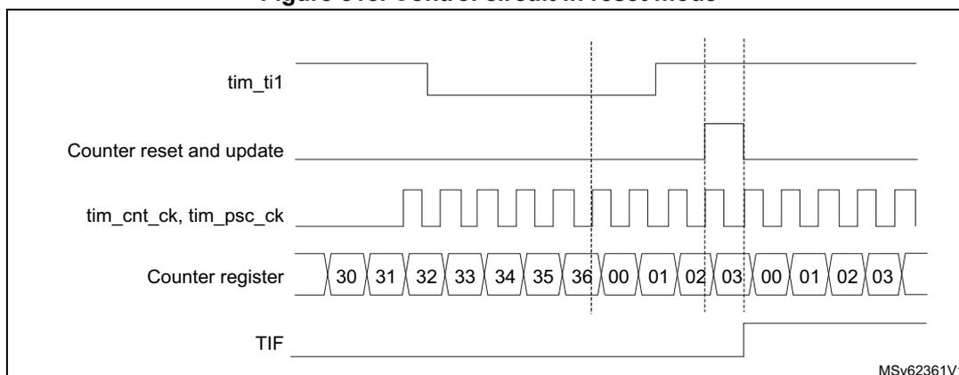
Slave mode: Gated mode
The counter can be enabled depending on the level of a selected input.
In the following example, the upcounter counts only when tim_ti1 input is low:
- 1. Configure the channel 1 to detect low levels on tim_ti1. Configure the input filter duration (in this example, we do not need any filter, so we keep IC1F = 0000). The capture prescaler is not used for triggering, so it does not need to be configured. The CC1S bits select the input capture source only, CC1S = 01 in TIMx_CCMR1 register. Write CC1P = 1 and CC1NP = 0 in TIMx_CCER register to validate the polarity (and detect low level only).
- 2. Configure the timer in gated mode by writing SMS = 101 in TIMx_SMCR register. Select tim_ti1 as the input source by writing TS = 00101 in TIMx_SMCR register.
- 3. Enable the counter by writing CEN = 1 in the TIMx_CR1 register (in gated mode, the counter does not start if CEN = 0, whatever is the trigger input level).
The counter starts counting on the internal clock as long as tim_ti1 is low and stops as soon as tim_ti1 becomes high. The TIF flag in the TIMx_SR register is set both when the counter starts or stops.
The delay between the rising edge on tim_ti1 and the actual stop of the counter is due to the resynchronization circuit on tim_ti1 input.
Figure 519. Control circuit in gated mode
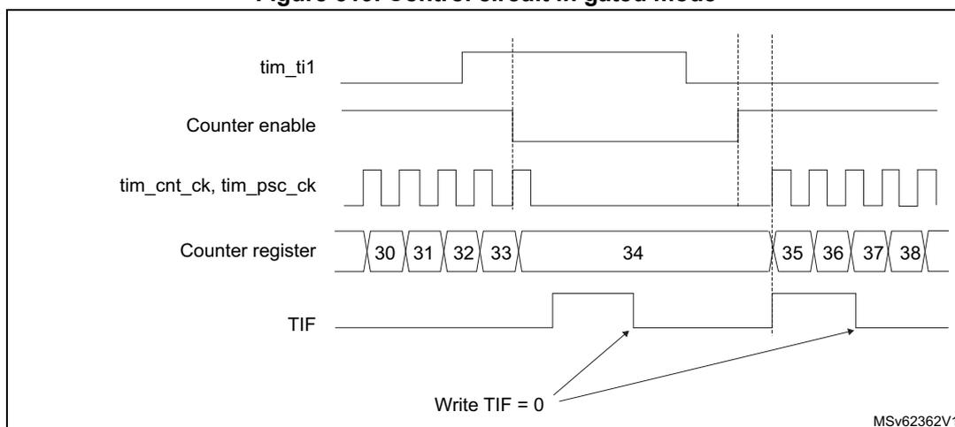
Note: The configuration “CCxP = CCxNP = 1” (detection of both rising and falling edges) does not have any effect in gated mode because gated mode acts on a level and not on an edge.
Slave mode: Trigger mode
The counter can start in response to an event on a selected input.
In the following example, the upcounter starts in response to a rising edge on tim_ti2 input:
- 1. Configure the channel 2 to detect rising edges on tim_ti2. Configure the input filter duration (in this example, we do not need any filter, so we keep IC2F = 0000). The capture prescaler is not used for triggering, so it does not need to be configured. CC2S bits are selecting the input capture source only, CC2S = 01 in TIMx_CCMR1 register. Write CC2P = 1 and CC2NP = 0 in TIMx_CCER register to validate the polarity (and detect low level only).
- 2. Configure the timer in trigger mode by writing SMS = 110 in TIMx_SMCR register. Select tim_ti2 as the input source by writing TS = 00110 in TIMx_SMCR register.
When a rising edge occurs on tim_ti2, the counter starts counting on the internal clock and the TIF flag is set.
The delay between the rising edge on tim_ti2 and the actual start of the counter is due to the resynchronization circuit on tim_ti2 input.
Figure 520. Control circuit in trigger mode
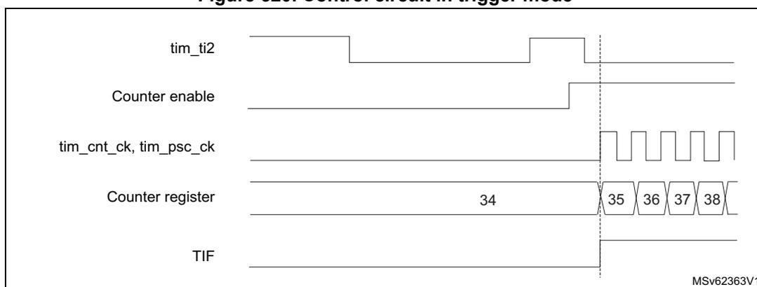
Slave mode selection preload for run-time encoder mode update
The SMS[3:0] bit can be preloaded. This is enabled by setting the SMSPE enable bit in the TIMx_SMCR register. The trigger for the transfer from SMS[3:0] preload to active value is the update event (UEV) occurring when the counter overflows.
Slave mode – combined reset + trigger mode
In this case, a rising edge of the selected trigger input (tim_trgi) reinitializes the counter, generates an update of the registers, and starts the counter.
This mode is used for one-pulse mode.
Slave mode – combined gated + reset mode
The counter clock is enabled when the trigger input (tim_trgi) is high. The counter stops and is reset as soon as the trigger becomes low. Both start and stop of the counter are controlled.
This mode is used to detect out-of-range PWM signal (duty cycle exceeding a maximum expected value).
Slave mode – external clock mode 2 + trigger mode
The external clock mode 2 can be used in addition to another slave mode (except external clock mode 1 and encoder mode). In this case, the tim_etr_in signal is used as external clock input, and another input can be selected as trigger input when operating in reset mode, gated mode, or trigger mode. It is recommended not to select tim_etr_in as tim_trgi through the TS bits of TIMx_SMCR register.
In the following example, the upcounter is incremented at each rising edge of the tim_etr_in signal as soon as a rising edge of tim_ti1 occurs:
- 1. Configure the external trigger input circuit by programming the TIMx_SMCR register as follows:
- – ETF = 0000: no filter.
- – ETPS = 00: prescaler disabled.
- – ETP = 0: detection of rising edges on tim_etr_in and ECE = 1 to enable the external clock mode 2.
- 2. Configure the channel 1 as follows, to detect rising edges on TI:
- – IC1F = 0000: no filter.
- – The capture prescaler is not used for triggering and does not need to be configured.
- – CC1S = 01 in TIMx_CCMR1 register to select only the input capture source.
- – CC1P = 0 and CC1NP = 0 in TIMx_CCER register to validate the polarity (and detect rising edge only).
- 3. Configure the timer in trigger mode by writing SMS = 110 in TIMx_SMCR register. Select tim_ti1 as the input source by writing TS = 00101 in TIMx_SMCR register.
A rising edge on tim_ti1 enables the counter and sets the TIF flag. The counter then counts on tim_etr_in rising edges.
The delay between the rising edge of the tim_etr_in signal and the actual reset of the counter is due to the resynchronization circuit on tim_etrp input.
Figure 521. Control circuit in external clock mode 2 + trigger mode
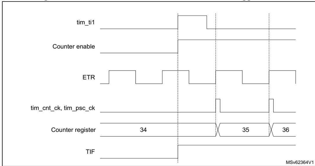
The timing diagram illustrates the control circuit in external clock mode 2 + trigger mode. The signals shown are:
- tim_ti1 : A signal that goes high to enable the counter.
- Counter enable : A signal that is high when the counter is enabled.
- ETR : An external trigger signal with multiple pulses.
- tim_cnt_ck, tim_psc_ck : The counter clock signal, which is derived from the ETR signal when the counter is enabled.
- Counter register : A register that increments its value (34, 35, 36) on each rising edge of the counter clock.
- TIF : A flag that is set when the counter is enabled while the ETR signal is high.
38.4.23 Timer synchronization
The TIMx timers are linked together internally for timer synchronization or chaining. When one timer is configured in Master mode, it can reset, start, stop, or clock the counter of another timer configured in Slave mode.
Figure 522 and Figure 523 show examples of master/slave timer connections.
Figure 522. Master/Slave timer example
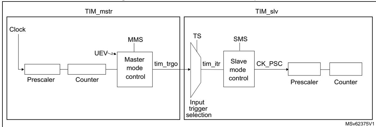
The block diagram shows the connection between a Master timer (TIM_mstr) and a Slave timer (TIM_slv):
- TIM_mstr : Consists of a Clock input, a Prescaler, a Counter, and a Master mode control block. The Master mode control block has inputs for MMS and UEV, and an output for tim_trgo.
- TIM_slv : Consists of an Input trigger selection block, a Slave mode control block, a Prescaler, and a Counter. The Input trigger selection block has an input for TS and an output for tim_itr.
- Connection : The tim_trgo output of the Master timer is connected to the TS input of the Slave timer's Input trigger selection block. The tim_itr output of the Slave timer is connected to the Slave mode control block.
- Slave Mode Control : The Slave mode control block has an output for CK_PSC, which is connected to the Prescaler of the Slave timer.
Figure 523. Master/slave connection example with 1 channel only timers
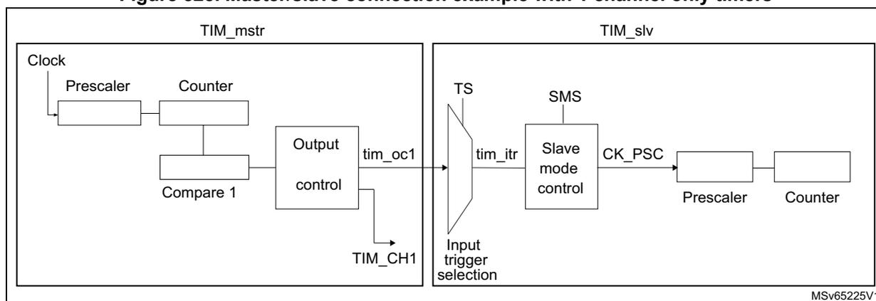
Note: The timers with one channel only (see Figure 523) do not feature a master mode. However, the tim_oc1 output signal can serve as trigger for slave timer (see TIMx internal trigger connection table in Section 38.4.2: TIM2/TIM3/TIM4 pins and internal signals). The tim_oc1 signal pulse width must be programmed to be at least two clock cycles of the destination timer, to make sure the slave timer detects the trigger. For instance, if the destination timer tim_ker_ck clock is four times slower than the source timer, the OC1 pulse width must be eight clock cycles.
Using one timer as prescaler for another timer
For example, TIM_mstr can be configured to act as a prescaler for TIM_slv. Refer to Figure 522. To do this:
- 1. Configure TIM_mstr in master mode so that it outputs a periodic trigger signal on each update event UEV. If MMS = 010 is written in the TIM_mstr_CR2 register, a rising edge is output on tim_trgo each time an update event is generated.
- 2. To connect the tim_trgo output of TIM_mstr to TIM_slv, TIM_slv must be configured in slave mode using ITR2 as internal trigger. This is selected through the TS bits in the TIM_slv_SMCR register (writing TS = 00010).
- 3. Then the slave mode controller must be put in external clock mode 1 (write SMS = 111 in the TIM_slv_SMCR register). This causes TIM_slv to be clocked by the rising edge of the periodic TIM_mstr trigger signal (which correspond to the TIM_mstr counter overflow).
- 4. Finally both timers must be enabled by setting their respective CEN bits (TIMx_CR1 register).
Note: If tim_ocx is selected on TIM_mstr as the trigger output (MMS = 1xx), its rising edge is used to clock the counter of TIM_slv.
Using one timer to enable another timer
In this example, we control the enable of TIM_slv with the output compare 1 of TIM_mstr. Refer to Figure 522 for connections. TIM_slv counts on the divided internal clock only when tim_oc1ref of TIM_mstr is high. Both counter clock frequencies are divided by 3 by the prescaler compared to tim_ker_ck ( \( f_{\text{tim\_cnt\_ck}} = f_{\text{tim\_ker\_ck}}/3 \) ).
- 1. Configure TIM_mstr master mode to send its output compare 1 reference (tim_oc1ref) signal as trigger output (MMS = 100 in the TIM_mstr_CR2 register).
- 2. Configure the TIM_mstr tim_oc1ref waveform (TIM_mstr_CCMR1 register).
- 3. Configure TIM_slv to get the input trigger from TIM_mstr (TS = 00010 in the TIM_slv_SMCR register).
- 4. Configure TIM_slv in gated mode (SMS = 101 in TIM_slv_SMCR register).
- 5. Enable TIM_slv by writing 1 in the CEN bit (TIM_slv_CR1 register).
- 6. Start TIM_mstr by writing 1 in the CEN bit (TIM_mstr_CR1 register).
Note: The slave timer counter clock is not synchronized with the master timer counter clock, this mode only affects the TIM_slv counter enable signal.
Figure 524. Gating TIM_slv with tim_oc1ref of TIM_mstr
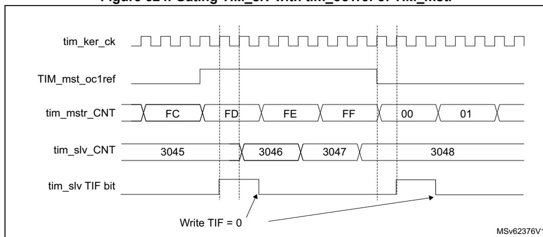
The timing diagram illustrates the operation of TIM_mstr and TIM_slv. The signals shown from top to bottom are:
1.
tim_ker_ck
: A continuous square wave clock signal.
2.
TIM_mst_oc1ref
: A gating signal that goes high for a duration of three clock cycles of tim_ker_ck.
3.
tim_mstr_CNT
: The master counter values, incrementing on each rising edge of tim_ker_ck through values FC, FD, FE, FF, 00, 01.
4.
tim_slv_CNT
: The slave counter values. It increments only when TIM_mst_oc1ref is high. It stays at 3045, then increments to 3046, 3047, and 3048 while the gate is open, then holds 3048 when the gate closes.
5.
tim_slv TIF bit
: A trigger interrupt flag that goes high when TIM_mst_oc1ref goes high. An arrow indicates a software action 'Write TIF = 0' which clears the flag while the gate is still high. The flag remains low thereafter.
The diagram is identified by the reference MSv62376V1.
In the example in Figure 524, the TIM_slv counter and prescaler are not initialized before being started. So they start counting from their current value. It is possible to start from a given value by resetting both timers before starting TIM_mstr. Then any value can be written in the timer counters. The timers can easily be reset by software using the UG bit in the TIMx_EGR registers.
In the next example (refer to Figure 525 ), we synchronize TIM_mstr and TIM_slv. TIM_mstr is the master and starts from 0. TIM_slv is the slave and starts from 0xE7. The prescaler ratio is the same for both timers. TIM_slv stops when TIM_mstr is disabled by writing 0 to the CEN bit in the TIM_mstr_CR1 register:
- 1. Configure TIM_mstr master mode to send its output compare 1 reference (tim_oc1ref) signal as trigger output (MMS = 100 in the TIM_mstr_CR2 register).
- 2. Configure the TIM_mstr tim_oc1ref waveform (TIM_mstr_CCMR1 register).
- 3. Configure TIM_slv to get the input trigger from TIM_mstr (TS = 00010 in the TIM_slv_SMCR register).
- 4. Configure TIM_slv in gated mode (SMS = 101 in TIM_slv_SMCR register).
- 5. Reset TIM_mstr by writing 1 in UG bit (TIM_mstr_EGR register).
- 6. Reset TIM_slv by writing 1 in UG bit (TIM_slv_EGR register).
- 7. Initialize TIM_slv to 0xE7 by writing 0xE7 in the TIM_slv counter (TIM_slv_CNT).
- 8. Enable TIM_slv by writing 1 in the CEN bit (TIM_slv_CR1 register).
- 9. Start TIM_mstr by writing 1 in the CEN bit (TIM_mstr_CR1 register).
- 10. Stop TIM_mstr by writing 0 in the CEN bit (TIM_mstr_CR1 register).
Figure 525. Gating TIM_slv with Enable of TIM_mstr
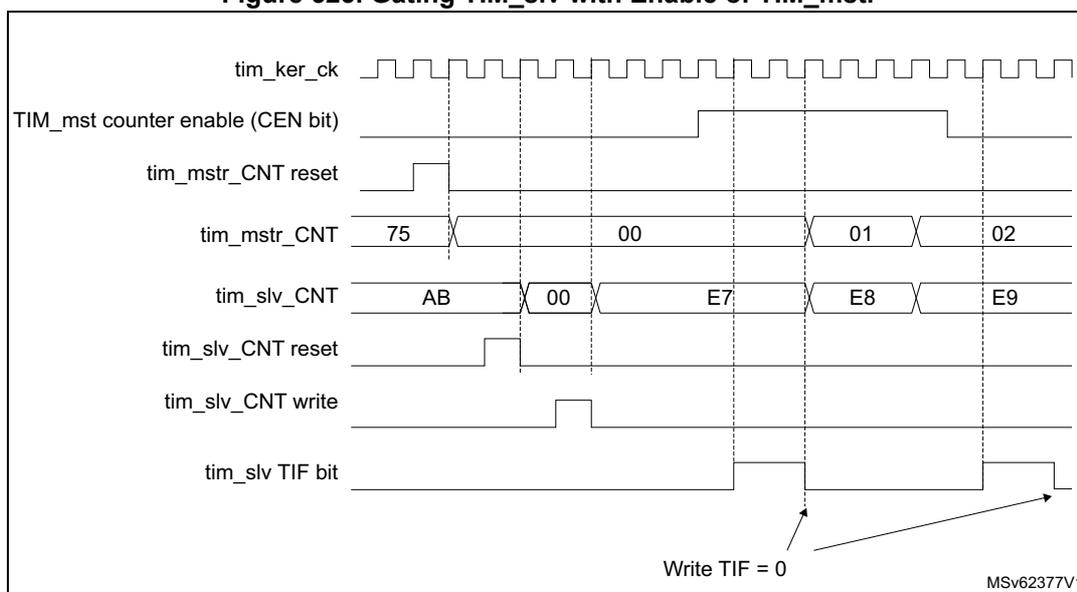
The timing diagram illustrates the synchronization of two timers, TIM_mstr and TIM_slv. The top signal is the kernel clock (tim_ker_ck). Below it is the TIM_mstr counter enable (CEN bit), which is high when the master timer is active. The master counter (tim_mstr_CNT) starts at 75, resets to 00, and then counts 01, 02. The slave counter (tim_slv_CNT) starts at AB, resets to 00, and then counts E7, E8, E9. The slave counter is enabled by the master counter's CEN bit. The slave TIF bit is set when the master counter reaches 02. An arrow points to the TIF bit with the text 'Write TIF = 0'. The diagram is labeled MSV62377V1.
Using one timer to start another timer
In this example, we set the enable of TIM_slv with the update event of TIM_mstr. Refer to Figure 522 for connections. TIM_slv starts counting from its current value (which can be nonzero) on the divided internal clock as soon as the update event is generated by TIM_mstr. When TIM_slv receives the trigger signal its CEN bit is automatically set and the counter counts until we write 0 to the CEN bit in the TIM_slv_CR1 register. Both counter clock frequencies are divided by 3 by the prescaler compared to tim_ker_ck ( \( f_{\text{tim\_cnt\_ck}} = f_{\text{tim\_ker\_ck}}/3 \) ).
- 1. Configure TIM_mstr master mode to send its update event (UEV) as trigger output (MMS = 010 in the TIM_mstr_CR2 register).
- 2. Configure the TIM_mstr period (TIM_mstr_ARR registers).
- 3. Configure TIM_slv to get the input trigger from TIM_mstr (TS = 00010 in the TIM_slv_SMCR register).
- 4. Configure TIM_slv in trigger mode (SMS = 110 in TIM_slv_SMCR register).
- 5. Start TIM_mstr by writing 1 in the CEN bit (TIM_mstr_CR1 register).
Figure 526. Triggering TIM_slv with update of TIM_mstr
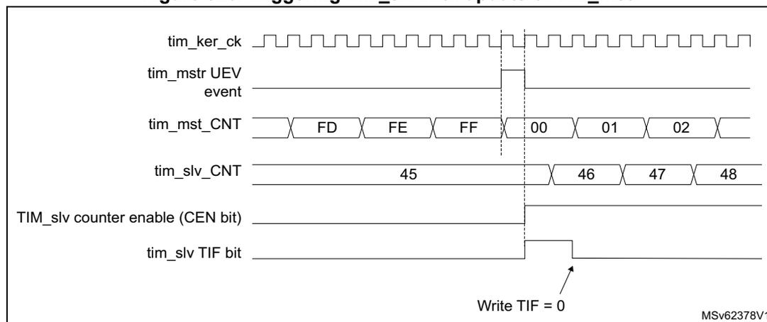
Timing diagram for Figure 526. The diagram shows the relationship between several signals over time:
- tim_ker_ck : A periodic clock signal.
- tim_mstr UEV event : A pulse that goes high when the master counter (tim_mst_CNT) reaches its period (FF) and overflows to 00.
- tim_mst_CNT : The master counter, which counts from FD to FE, FF, 00, 01, 02.
- tim_slv_CNT : The slave counter, which counts from 45 to 46, 47, 48. It is triggered by the master counter's update event.
- TIM_slv counter enable (CEN bit) : A signal that is set high at the beginning of the sequence.
- tim_slv TIF bit : A signal that goes high when the slave counter is triggered and is then cleared by a write operation, labeled "Write TIF = 0".
MSv62378V1
As in the previous example, both counters can be initialized before starting counting.
Figure 527 shows the behavior with the same configuration as in Figure 526 but in trigger mode (SMS = 110 in the TIM_slv_SMCR register) instead of gated mode.
Figure 527. Triggering TIM_slv with Enable of TIM_mstr
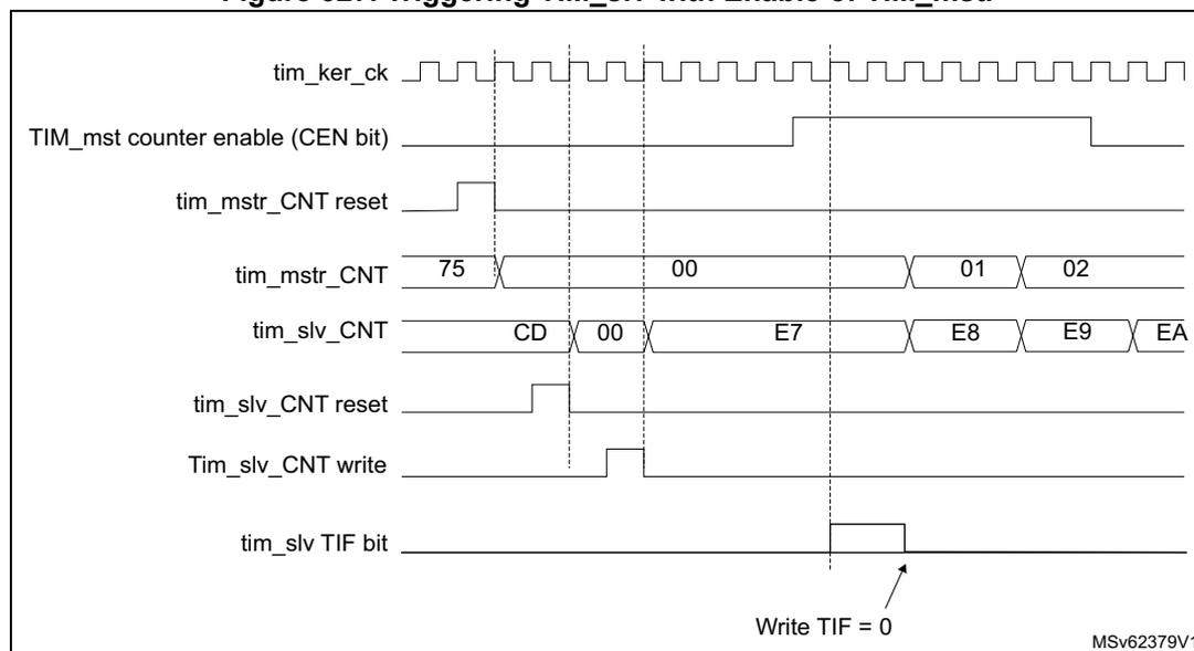
Timing diagram for Figure 527. The diagram shows the relationship between several signals over time:
- tim_ker_ck : A periodic clock signal.
- TIM_mst counter enable (CEN bit) : A signal that is set high at the beginning of the sequence.
- tim_mstr_CNT reset : A pulse that goes high to reset the master counter.
- tim_mstr_CNT : The master counter, which is reset to 75 and then counts from 00 to 01, 02.
- tim_slv_CNT : The slave counter, which counts from CD to 00, E7, E8, E9, EA. It is triggered by the master counter's enable (CEN bit).
- tim_slv_CNT reset : A pulse that goes high to reset the slave counter.
- Tim_slv_CNT write : A signal that is used to write the value E7 into the slave counter.
- tim_slv TIF bit : A signal that goes high when the slave counter is triggered and is then cleared by a write operation, labeled "Write TIF = 0".
MSv62379V1
Starting two timers synchronously in response to an external trigger
In this example, we set the enable of TIM_mstr when its tim_ti1 input rises, and the enable of TIM_slv with the enable of TIM_mstr. Refer to Figure 522 for connections. To ensure the counters are aligned, TIM_mstr must be configured in Master/Slave mode (slave with respect to tim_ti1, master with respect to TIM_slv):
- 1. Configure TIM_mstr master mode to send its enable as trigger output (MMS = 001 in the TIM_mstr_CR2 register).
- 2. Configure TIM_mstr slave mode to get the input trigger from tim_ti1 (TS = 00100 in the TIM_mstr_SMCR register).
- 3. Configure TIM_mstr in trigger mode (SMS = 110 in the TIM_mstr_SMCR register).
- 4. Configure the TIM_mstr in Master/Slave mode by writing MSM = 1 (TIM_mstr_SMCR register).
- 5. Configure TIM_slv to get the input trigger from TIM_mstr (TS = 00000 in the TIM_slv_SMCR register).
- 6. Configure TIM_slv in trigger mode (SMS = 110 in the TIM_slv_SMCR register).
When a rising edge occurs on tim_ti1 (TIM_mstr), both counters start counting synchronously on the internal clock and both TIF flags are set.
Note: In this example both timers are initialized before starting (by setting their respective UG bits). Both counters starts from 0, but an offset can easily be inserted between them by writing any of the counter registers (TIMx_CNT). One can see that the master/slave mode inserts a delay between CNT_EN and CK_PSC on TIM_mstr.
Figure 528. Triggering TIM_mstr and TIM_slv with TIM_mstr tim_ti1 input
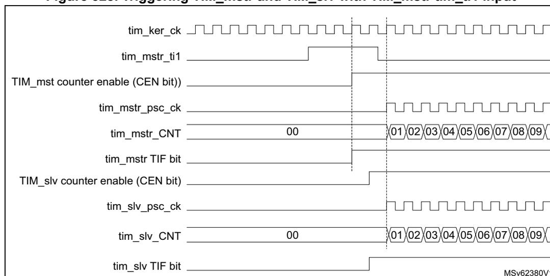
Note: The clock of the slave peripherals (such as timer, ADC) receiving the tim_trgo signal must be enabled prior to receive events from the master timer, and the clock frequency (prescaler) must not be changed on-the-fly while triggers are received from the master timer.
38.4.24 ADC triggers
The timer can generate an ADC triggering event with various internal signals, such as reset, enable or compare events.
Note: The clock of the slave peripherals (such as timer, ADC) receiving the tim_trgo signal must be enabled prior to receive events from the master timer, and the clock frequency (prescaler) must not be changed on-the-fly while triggers are received from the master timer.
38.4.25 ADC synchronization
The timer operation can be synchronized to the ADC clock to trigger jitter-free ADC sampling. This function is enabled using the ADSYNC bit in the TIMx_CR2 register.
This feature is useful when the timers and the ADCs are operating with semisynchronous clocks (clocks derived from a same source with integer ratio tim_ker_ck/adc_ker_ck), for instance adc_ker_ck = 75 MHz and tim_ker_ck = 150 MHz or 300 MHz.
ADSYNC must also be set when both peripherals are operating at the same frequency from the same clock source, when jitter-free operation is needed.
ADSYNC must not be set and jitter-free operation is not supported in the following cases:
- • When the clock ratio is not an integer (for example adc_ker_ck = 75 MHz and tim_ker_ck = 100 MHz): in this case, the sampling point jitter due to the timer to ADC signal resynchronization is 1 adc_ker_ck period maximum.
- • When the ADC is operating in asynchronous mode (adc_ker_ck uncorrelated with tim_ker_ck): in this case, the sampling point jitter due to the timer to ADC signal resynchronization is 1 adc_ker_ck period maximum.
When ADSYNC = 1, the timer operation is slightly changed: the counter enable and counter reset events are aligned to the adc_ker_ck ADC clock, to avoid any phase shift due to clocks enable in the RCC.
Jitter-free operation is guaranteed only when one of the two requirements below is met (depending on the selected trigger source):
- 1. The counter period must be a multiple of the ADC clock period.
- 2. The compare value must be a multiple of the ADC clock period.
Note: If none of the two above requirements is met, the trigger is still generated, but the latency is not constant and varies with the timer and ADC clocks phase shift.
Programming guidelines
The ADC synchronization feature must not be modified during run-time, once the counter is enabled and once the ADC has been configured for receiving triggers from the timer.
It is mandatory to follow the procedure below to use the ADC synchronization:
- 1. Enable the destination ADC clock.
- 2. Configure the timer and set the ADSYNC bit.
- 3. Configure the ADC and enable it (using ADSTART and/or JADSTART bits).
- 4. Start the timer (with the CEN counter enable bit).
38.4.26 DMA burst mode
The TIMx timers have the capability to generate multiple DMA requests upon a single event. The main purpose is to be able to reprogram part of the timer multiple times without software overhead, but it can also be used to read several registers in a row, at regular intervals.
The DMA controller destination is unique and must point to the virtual register TIMx_DMAR. On a given timer event, the timer launches a sequence of DMA requests (burst). Each write into the TIMx_DMAR register is actually redirected to one of the timer registers.
The DBL[4:0] bits in the TIMx_DCR register set the DMA burst length. The timer recognizes a burst transfer when a read or a write access is done to the TIMx_DMAR address), i.e. the number of transfers (either in half-words or in bytes).
The DBA[4:0] bits in the TIMx_DCR registers define the DMA base address for DMA transfers (when read/write accesses are done through the TIMx_DMAR address). DBA is defined as an offset starting from the address of the TIMx_CR1 register:
Example:
00000: TIMx_CR1
00001: TIMx_CR2
00010: TIMx_SMCR
The DBSS[3:0] bits in the TIMx_DCR register defines the interrupt source that triggers the DMA burst transfers (see Section 38.5.23: TIMx DMA control register (TIMx_DCR)(x = 2 to 4) for details).
As an example, the timer DMA burst feature is used to update the contents of the CCRx registers (x = 2, 3, 4) upon an update event, with the DMA transferring half words into the CCRx registers.
This is done in the following steps:
- 1. Configure the corresponding DMA channel as follows:
- – DMA channel peripheral address is the DMAR register address.
- – DMA channel memory address is the address of the buffer in the RAM containing the data to be transferred by DMA into CCRx registers.
- – Number of data to transfer = 3 (See note below).
- – Circular mode disabled.
- 2. Configure the DCR register by configuring the DBA and DBL bitfields as follows: DBL = 3 transfers, DBA = 0xE and DBSS = 1.
- 3. Enable the TIMx update DMA request (set the UDE bit in the DIER register).
- 4. Enable TIMx.
- 5. Enable the DMA channel.
This example is for the case where every CCRx register has to be updated once. If every CCRx register is to be updated twice for example, the number of data to transfer must be 6. Let's take the example of a buffer in the RAM containing data1, data2, data3, data4, data5, and data6. The data is transferred to the CCRx registers as follows: on the first update DMA request, data1 is transferred to CCR2, data2 is transferred to CCR3, data3 is transferred to CCR4 and on the second update DMA request, data4 is transferred to CCR2, data5 is transferred to CCR3, and data6 is transferred to CCR4.
Note: A null value can be written to the reserved registers.
38.4.27 TIM2/TIM3/TIM4 DMA requests
The TIM2/TIM3/TIM4 can generate a DMA requests, as shown in Table 415 .
Table 415. DMA request
| DMA request signal | DMA request | Enable control bit |
|---|---|---|
| tim_upd_dma | Update | UDE |
| tim_cc1_dma | Capture/compare 1 | CC1DE |
| tim_cc2_dma | Capture/compare 2 | CC2DE |
| tim_cc3_dma | Capture/compare 3 | CC3DE |
| tim_cc4_dma | Capture/compare 4 | CC4DE |
| tim_trgi_dma | Trigger | TDE |
Note: Some timer's DMA requests may not be connected to the DMA controller. Refer to the DMA section(s) for more details.
38.4.28 Debug mode
When the microcontroller enters debug mode (Cortex-M33 core halted), the TIMx counter can either continue to work normally or stops.
The behavior in debug mode can be programmed with a dedicated configuration bit per timer in the Debug support (DBG) module.
For more details, refer to section Debug support (DBG).
38.4.29 TIM2/TIM3/TIM4 low-power modes
Table 416. Effect of low-power modes on TIM2/TIM3/TIM4
| Mode | Description |
|---|---|
| Sleep | No effect, peripheral is active. The interrupts can cause the device to exit from Sleep mode. |
| Stop | The timer operation is stopped and the register content is kept. No interrupt can be generated. |
| Standby | The timer is powered-down and must be reinitialized after exiting the Standby mode. |
38.4.30 TIM2/TIM3/TIM4 interrupts
The TIM2/TIM3/TIM4 can generate multiple interrupts, as shown in Table 417 .
Table 417. Interrupt requests
| Interrupt acronym | Interrupt event | Event flag | Enable control bit | Interrupt clear method | Exit from Sleep mode | Exit from Stop and Standby mode |
|---|---|---|---|---|---|---|
| TIM_UP | Update | UIF | UIE | write 0 in UIF | Yes | No |
| TIM_CC | Capture/compare 1 | CC1IF | CC1IE | write 0 in CC1IF | Yes | No |
| Capture/compare 2 | CC2IF | CC2IE | write 0 in CC2IF | Yes | No | |
| Capture/compare 3 | CC3IF | CC3IE | write 0 in CC3IF | Yes | No | |
| Capture/compare 4 | CC4IF | CC4IE | write 0 in CC4IF | Yes | No | |
| TIM_TRG | Trigger | TIF | TIE | write 0 in TIF | Yes | No |
| TIM_DIR _IDX | Index | IDXF | IDXIE | write 0 in IDXF | Yes | No |
| Direction | DIRF | DIRIE | write 0 in DIRF | Yes | No | |
| TIM_IERR | Index Error | IERRF | IERRIE | write 0 in IERRF | Yes | No |
| TIM_TER | Transition Error | TERRF | TERRIE | write 0 in TERRF | Yes | No |
38.5 TIM2/TIM3/TIM4 registers
Refer to Section 1.2 for a list of abbreviations used in register descriptions.
The peripheral registers can be accessed by half-words (16-bit) or words (32-bit).
38.5.1 TIMx control register 1 (TIMx_CR1)(x = 2 to 4)
Address offset: 0x000
Reset value: 0x0000
| 15 | 14 | 13 | 12 | 11 | 10 | 9 | 8 | 7 | 6 | 5 | 4 | 3 | 2 | 1 | 0 |
|---|---|---|---|---|---|---|---|---|---|---|---|---|---|---|---|
| Res. | Res. | Res. | DITH EN | UIFRE MAP | Res. | CKD[1:0] | ARPE | CMS[1:0] | DIR | OPM | URS | UDIS | CEN | ||
| rw | rw | rw | rw | rw | rw | rw | rw | rw | rw | rw | rw | ||||
Bits 15:13 Reserved, must be kept at reset value.
Bit 12 DITHEN : Dithering Enable
0: Dithering disabled
1: Dithering enabled
Note: The DITHEN bit can only be modified when CEN bit is reset.
Bit 11 UIFREMAP : UIF status bit remapping
0: No remapping. UIF status bit is not copied to TIMx_CNT register bit 31.
1: Remapping enabled. UIF status bit is copied to TIMx_CNT register bit 31.
Bit 10 Reserved, must be kept at reset value.
Bits 9:8 CKD[1:0] : Clock division
This bitfield indicates the division ratio between the timer clock (tim_ker_ck) frequency and sampling clock used by the digital filters (tim_etr_in, tim_tix),
00: \( t_{DTS} = t_{tim\_ker\_ck} \)
01: \( t_{DTS} = 2 \times t_{tim\_ker\_ck} \)
10: \( t_{DTS} = 4 \times t_{tim\_ker\_ck} \)
11: Reserved
Bit 7 ARPE : Autoreload preload enable
0: TIMx_ARR register is not buffered
1: TIMx_ARR register is buffered
Bits 6:5 CMS[1:0] : Center-aligned mode selection
00: Edge-aligned mode. The counter counts up or down depending on the direction bit (DIR).
01: Center-aligned mode 1. The counter counts up and down alternatively. Output compare interrupt flags of channels configured in output (CCxS = 00 in TIMx_CCMRx register) are set only when the counter is counting down.
10: Center-aligned mode 2. The counter counts up and down alternatively. Output compare interrupt flags of channels configured in output (CCxS = 00 in TIMx_CCMRx register) are set only when the counter is counting up.
11: Center-aligned mode 3. The counter counts up and down alternatively. Output compare interrupt flags of channels configured in output (CCxS = 00 in TIMx_CCMRx register) are set both when the counter is counting up or down.
Note: It is not allowed to switch from edge-aligned mode to center-aligned mode as long as the counter is enabled (CEN = 1)
Bit 4 DIR : Direction
0: Counter used as upcounter
1: Counter used as downcounter
Note: This bit is read only when the timer is configured in Center-aligned mode or Encoder mode.
Bit 3 OPM : One-pulse mode
0: Counter is not stopped at update event
1: Counter stops counting at the next update event (clearing the bit CEN)
Bit 2 URS : Update request source
This bit is set and cleared by software to select the UEV event sources.
0: Any of the following events generate an update interrupt or DMA request if enabled.
These events can be:
- - Counter overflow/underflow
- - Setting the UG bit
- - Update generation through the slave mode controller
1: Only counter overflow/underflow generates an update interrupt or DMA request if enabled.
Bit 1 UDIS : Update disable
This bit is set and cleared by software to enable/disable UEV event generation.
0: UEV enabled. The Update (UEV) event is generated by one of the following events:
- - Counter overflow/underflow
- - Setting the UG bit
- - Update generation through the slave mode controller
Buffered registers are then loaded with their preload values.
1: UEV disabled. The Update event is not generated, shadow registers keep their value (ARR, PSC, CCRx). However the counter and the prescaler are reinitialized if the UG bit is set or if a hardware reset is received from the slave mode controller.
Bit 0 CEN : Counter enable
0: Counter disabled
1: Counter enabled
Note: External clock, gated mode and encoder mode can work only if the CEN bit has been previously set by software. However trigger mode can set the CEN bit automatically by hardware.
CEN is cleared automatically in one-pulse mode, when an update event occurs.
38.5.2 TIMx control register 2 (TIMx_CR2)(x = 2 to 4)
Address offset: 0x004
Reset value: 0x0000 0000
| 31 | 30 | 29 | 28 | 27 | 26 | 25 | 24 | 23 | 22 | 21 | 20 | 19 | 18 | 17 | 16 |
|---|---|---|---|---|---|---|---|---|---|---|---|---|---|---|---|
| Res. | Res. | Res. | AD SYNC | Res. | Res. | MMS[3] | Res. | Res. | Res. | Res. | Res. | Res. | Res. | Res. | Res. |
| rw | rw | ||||||||||||||
| 15 | 14 | 13 | 12 | 11 | 10 | 9 | 8 | 7 | 6 | 5 | 4 | 3 | 2 | 1 | 0 |
| Res. | Res. | Res. | Res. | Res. | Res. | Res. | Res. | TI1S | MMS[2:0] | CCDS | Res. | Res. | Res. | ||
| rw | rw | rw | rw | rw | |||||||||||
Bits 31:29 Reserved, must be kept at reset value.
Bit 28 ADSYNC : ADC synchronization
0: The timer operates independently from the ADC
1: The timer operation is synchronized with the ADC clock to provide jitter-free sampling point. This mode can be enabled only with specific ADC / timer clock relationship. Refer to Section 38.4.25 for requirements.
The ADSYNC must not modified when the counter is enabled (CEN bit is set).
Bits 27:26 Reserved, must be kept at reset value.
Bits 24:8 Reserved, must be kept at reset value.
Bit 7 TI1S : tim_ti1 selection
0: The tim_ti1_in[15:0] multiplexer output is to tim_ti1 input
1: The tim_ti1_in[15:0], tim_ti2_in[15:0] and tim_ti3_in[15:0] multiplexers outputs are XORed and connected to the tim_ti1 input. See also Section 37.3.29: Interfacing with Hall sensors .
Bits 25, 6, 5, 4 MMS[3:0] : Master mode selection
These bits are used to select the information to be sent in master mode to slave timers for synchronization (tim_trgo). The combination is as follows:
0000: Reset - the UG bit from the TIMx_EGR register is used as trigger output (tim_trgo). If the reset is generated by the trigger input (slave mode controller configured in reset mode) then the signal on tim_trgo is delayed compared to the actual reset.
0001: Enable - the Counter enable signal, CNT_EN, is used as trigger output (tim_trgo). It is useful to start several timers at the same time or to control a window in which a slave timer is enabled. The Counter Enable signal is generated by a logic AND between CEN control bit and the trigger input when configured in gated mode.
When the Counter Enable signal is controlled by the trigger input, there is a delay on tim_trgo, except if the master/slave mode is selected (see the MSM bit description in TIMx_SMCR register).
0010: Update - The update event is selected as trigger output (tim_trgo). For instance a master timer can then be used as a prescaler for a slave timer.
0011: Compare Pulse - The trigger output send a positive pulse when the CC1IF flag is to be set (even if it was already high), as soon as a capture or a compare match occurred (tim_trgo).
0100: Compare - tim_oc1refc signal is used as trigger output (tim_trgo)
0101: Compare - tim_oc2refc signal is used as trigger output (tim_trgo)
0110: Compare - tim_oc3refc signal is used as trigger output (tim_trgo)
0111: Compare - tim_oc4refc signal is used as trigger output (tim_trgo)
1000: Encoder clock output - The encoder clock signal is used as trigger output (tim_trgo). This code is valid for the following SMS[3:0] values: 0001, 0010, 0011, 1010, 1011, 1100, 1101, 1110, 1111. Any other SMS[3:0] code is not allowed and may lead to unexpected behavior.
Others: Reserved
Note: The clock of the slave timer or ADC must be enabled prior to receive events from the master timer, and must not be changed on-the-fly while triggers are received from the master timer.
Bit 3 CCDS : Capture/compare DMA selection
0: CCx DMA request sent when CCx event occurs
1: CCx DMA requests sent when update event occurs
Bits 2:0 Reserved, must be kept at reset value.
38.5.3 TIMx slave mode control register (TIMx_SMCR)(x = 2 to 4)
Address offset: 0x008
Reset value: 0x0000 0000
| 31 | 30 | 29 | 28 | 27 | 26 | 25 | 24 | 23 | 22 | 21 | 20 | 19 | 18 | 17 | 16 |
|---|---|---|---|---|---|---|---|---|---|---|---|---|---|---|---|
| Res. | Res. | Res. | Res. | Res. | Res. | SMSPS | SMSPE | Res. | Res. | TS[4:3] | Res. | Res. | Res. | SMS[3] | |
| rw | rw | rw | rw | rw | |||||||||||
| 15 | 14 | 13 | 12 | 11 | 10 | 9 | 8 | 7 | 6 | 5 | 4 | 3 | 2 | 1 | 0 |
| ETP | ECE | ETPS[1:0] | ETF[3:0] | MSM | TS[2:0] | OCCS | SMS[2:0] | ||||||||
| rw | rw | rw | rw | rw | rw | rw | rw | rw | rw | rw | rw | rw | rw | rw | rw |
Bits 31:26 Reserved, must be kept at reset value.
Bit 25 SMSPS : SMS preload source
This bit selects whether the events that triggers the SMS[3:0] bitfield transfer from preload to active
0: The transfer is triggered by the Timer's Update event
1: The transfer is triggered by the Index event
Bit 24 SMSPE : SMS preload enable
This bit selects whether the SMS[3:0] bitfield is preloaded
0: SMS[3:0] bitfield is not preloaded
1: SMS[3:0] preload is enabled
Bits 23:22 Reserved, must be kept at reset value.
Bits 19:17 Reserved, must be kept at reset value.
Bit 15 ETP : External trigger polarity
This bit selects whether tim_etr_in or tim_etr_in is used for trigger operations
0: tim_etr_in is non-inverted, active at high level or rising edge
1: tim_etr_in is inverted, active at low level or falling edge
Bit 14 ECE : External clock enable
This bit enables External clock mode 2.
0: External clock mode 2 disabled
1: External clock mode 2 enabled. The counter is clocked by any active edge on the tim_etrf signal.
Note: Setting the ECE bit has the same effect as selecting external clock mode 1 with tim_trgi connected to tim_etrf (SMS = 111 and TS = 00111).
It is possible to simultaneously use external clock mode 2 with the following slave modes: reset mode, gated mode and trigger mode. Nevertheless, tim_trgi must not be connected to tim_etrf in this case (TS bits must not be 00111).
If external clock mode 1 and external clock mode 2 are enabled at the same time, the external clock input is tim_etrf .
Bits 13:12 ETPS[1:0] : External trigger prescaler
External trigger signal tim_etrp frequency must be at most 1/4 of tim_ker_ck frequency. A prescaler can be enabled to reduce tim_etrp frequency. It is useful when inputting fast external clocks on tim_etr_in .
00: Prescaler OFF
01: tim_etrp frequency divided by 2
10: tim_etrp frequency divided by 4
11: tim_etrp frequency divided by 8
Bits 11:8 ETF[3:0] : External trigger filterThis bitfield then defines the frequency used to sample tim_etrp signal and the length of the digital filter applied to tim_etrp. The digital filter is made of an event counter in which N consecutive events are needed to validate a transition on the output:
0000: No filter, sampling is done at \( f_{DTS} \)
0001: \( f_{SAMPLING} = f_{tim\_ker\_ck} \) , N = 2
0010: \( f_{SAMPLING} = f_{tim\_ker\_ck} \) , N = 4
0011: \( f_{SAMPLING} = f_{tim\_ker\_ck} \) , N = 8
0100: \( f_{SAMPLING} = f_{DTS}/2 \) , N = 6
0101: \( f_{SAMPLING} = f_{DTS}/2 \) , N = 8
0110: \( f_{SAMPLING} = f_{DTS}/4 \) , N = 6
0111: \( f_{SAMPLING} = f_{DTS}/4 \) , N = 8
1000: \( f_{SAMPLING} = f_{DTS}/8 \) , N = 6
1001: \( f_{SAMPLING} = f_{DTS}/8 \) , N = 8
1010: \( f_{SAMPLING} = f_{DTS}/16 \) , N = 5
1011: \( f_{SAMPLING} = f_{DTS}/16 \) , N = 6
1100: \( f_{SAMPLING} = f_{DTS}/16 \) , N = 8
1101: \( f_{SAMPLING} = f_{DTS}/32 \) , N = 5
1110: \( f_{SAMPLING} = f_{DTS}/32 \) , N = 6
1111: \( f_{SAMPLING} = f_{DTS}/32 \) , N = 8
Bit 7 MSM : Master/Slave mode0: No action
1: The effect of an event on the trigger input (tim_trgi) is delayed to allow a perfect synchronization between the current timer and its slaves (through tim_trgo). It is useful if we want to synchronize several timers on a single external event.
Bits 21, 20, 6, 5, 4 TS[4:0] : Trigger selectionThis bitfield selects the trigger input to be used to synchronize the counter.
- 00000: Internal trigger 0 (tim_itr0)
- 00001: Internal trigger 1 (tim_itr1)
- 00010: Internal trigger 2 (tim_itr2)
- 00011: Internal trigger 3 (tim_itr3)
- 00100: tim_ti1 edge detector (tim_ti1f_ed)
- 00101: Filtered timer input 1 (tim_ti1fp1)
- 00110: Filtered timer input 2 (tim_ti2fp2)
- 00111: External trigger input (tim_etr)
- 01000: Internal trigger 4 (tim_itr4)
- 01001: Internal trigger 5 (tim_itr5)
- 01010: Internal trigger 6 (tim_itr6)
- 01011: Internal trigger 7 (tim_itr7)
- 01100: Internal trigger 8 (tim_itr8)
- 01101: Internal trigger 9 (tim_itr9)
- 01110: Internal trigger 10 (tim_itr10)
- 01111: Internal trigger 11 (tim_itr11)
- 10000: Internal trigger 12 (tim_itr12)
- 10001: Internal trigger 13 (tim_itr13)
- 10010: Internal trigger 14 (tim_itr14)
- 10011: Internal trigger 15 (tim_itr15)
Others: Reserved
See Section 38.4.2: TIM2/TIM3/TIM4 pins and internal signals for product specific implementation details.
Note: These bits must be changed only when they are not used (for example when SMS = 000) to avoid wrong edge detections at the transition.
Bit 3 OCCS : OREF clear selectionThis bit is used to select the OREF clear source
- 0: tim_ocref_clr_int is connected to the tim_ocref_clr input
- 1: tim_ocref_clr_int is connected to tim_etr
Note: If the OREF clear selection feature is not supported, this bit is reserved and forced by hardware to 0. Section 38.3: TIM2/TIM3/TIM4 implementation .
Bits 16, 2, 1, 0 SMS[3:0] : Slave mode selection
When external signals are selected the active edge of the trigger signal (tim_trgi) is linked to the polarity selected on the external input (refer to ETP bit in TIMx_SMCR for tim_etr_in and CCxP/CCxNP bits in TIMx_CCER register for tim_ti1fp1 and tim_ti2fp2).
0000: Slave mode disabled - if CEN = 1 then the prescaler is clocked directly by the internal clock.
0001: Encoder mode 1 - Counter counts up/down on tim_ti1fp1 edge depending on tim_ti2fp2 level.
0010: Encoder mode 2 - Counter counts up/down on tim_ti2fp2 edge depending on tim_ti1fp1 level.
0011: Encoder mode 3 - Counter counts up/down on both tim_ti1fp1 and tim_ti2fp2 edges depending on the level of the other input.
0100: Reset mode - Rising edge of the selected trigger input (tim_trgi) reinitializes the counter and generates an update of the registers.
0101: Gated mode - The counter clock is enabled when the trigger input (tim_trgi) is high. The counter stops (but is not reset) as soon as the trigger becomes low. Both start and stop of the counter are controlled.
0110: Trigger mode - The counter starts at a rising edge of the trigger tim_trgi (but it is not reset). Only the start of the counter is controlled.
0111: External clock mode 1 - Rising edges of the selected trigger (tim_trgi) clock the counter.
1000: Combined reset + trigger mode - Rising edge of the selected trigger input (tim_trgi) reinitializes the counter, generates an update of the registers and starts the counter.
1001: Combined gated + reset mode - The counter clock is enabled when the trigger input (tim_trgi) is high. The counter stops and is reset) as soon as the trigger becomes low. Both start and stop of the counter are controlled.
1010: Encoder mode: Clock plus direction, x2 mode.
1011: Encoder mode: Clock plus direction, x1 mode, tim_ti2fp2 edge sensitivity is set by CC2P.
1100: Encoder mode: Directional clock, x2 mode.
1101: Encoder mode: Directional clock, x1 mode, tim_ti1fp1 and tim_ti2fp2 edge sensitivity is set by CC1P and CC2P.
1110: Quadrature encoder mode: x1 mode, counting on tim_ti1fp1 edges only, edge sensitivity is set by CC1P.
1111: Quadrature encoder mode: x1 mode, counting on tim_ti2fp2 edges only, edge sensitivity is set by CC2P.
Note: The gated mode must not be used if tim_ti1f_ed is selected as the trigger input (TS = 00100). Indeed, tim_ti1f_ed outputs 1 pulse for each transition on tim_ti1f, whereas the gated mode checks the level of the trigger signal.
Note: The clock of the slave peripherals (such as timer, ADC) receiving the tim_trgo signal must be enabled prior to receive events from the master timer, and the clock frequency (prescaler) must not be changed on-the-fly while triggers are received from the master timer.
38.5.4 TIMx DMA/Interrupt enable register (TIMx_DIER)(x = 2 to 4)
Address offset: 0x00C
Reset value: 0x0000 0000
| 31 | 30 | 29 | 28 | 27 | 26 | 25 | 24 | 23 | 22 | 21 | 20 | 19 | 18 | 17 | 16 |
|---|---|---|---|---|---|---|---|---|---|---|---|---|---|---|---|
| Res. | Res. | Res. | Res. | Res. | Res. | Res. | Res. | TERR IE | IERR IE | DIRIE | IDXIE | Res. | Res. | Res. | Res. |
| rw | rw | rw | rw | ||||||||||||
| 15 | 14 | 13 | 12 | 11 | 10 | 9 | 8 | 7 | 6 | 5 | 4 | 3 | 2 | 1 | 0 |
| Res. | TDE | Res. | CC4DE | CC3DE | CC2DE | CC1DE | UDE | Res. | TIE | Res. | CC4IE | CC3IE | CC2IE | CC1IE | UIE |
| rw | rw | rw | rw | rw | rw | rw | rw | rw | rw | rw | rw |
Bits 31:24 Reserved, must be kept at reset value.
Bit 23 TERRIE : Transition error interrupt enable
0: Transition error interrupt disabled
1: Transition error interrupt enabled
Bit 22 IERRIE : Index error interrupt enable
0: Index error interrupt disabled
1: Index error interrupt enabled
Bit 21 DIRIE : Direction change interrupt enable
0: Direction change interrupt disabled
1: Direction change interrupt enabled
Bit 20 IDXIE : Index interrupt enable
0: Index interrupt disabled
1: Index interrupt enabled
Bits 19:15 Reserved, must be kept at reset value.
Bit 14 TDE : Trigger DMA request enable
0: Trigger DMA request disabled.
1: Trigger DMA request enabled.
Bit 13 Reserved, must be kept at reset value.
Bit 12 CC4DE : Capture/Compare 4 DMA request enable
0: CC4 DMA request disabled.
1: CC4 DMA request enabled.
Bit 11 CC3DE : Capture/Compare 3 DMA request enable
0: CC3 DMA request disabled.
1: CC3 DMA request enabled.
Bit 10 CC2DE : Capture/Compare 2 DMA request enable
0: CC2 DMA request disabled.
1: CC2 DMA request enabled.
Bit 9 CC1DE : Capture/Compare 1 DMA request enable
0: CC1 DMA request disabled.
1: CC1 DMA request enabled.
Bit 8 UDE : Update DMA request enable
0: Update DMA request disabled.
1: Update DMA request enabled.
- Bit 7 Reserved, must be kept at reset value.
- Bit 6
TIE
: Trigger interrupt enable
0: Trigger interrupt disabled.
1: Trigger interrupt enabled. - Bit 5 Reserved, must be kept at reset value.
- Bit 4
CC4IE
: Capture/Compare 4 interrupt enable
0: CC4 interrupt disabled.
1: CC4 interrupt enabled. - Bit 3
CC3IE
: Capture/Compare 3 interrupt enable
0: CC3 interrupt disabled.
1: CC3 interrupt enabled. - Bit 2
CC2IE
: Capture/Compare 2 interrupt enable
0: CC2 interrupt disabled.
1: CC2 interrupt enabled. - Bit 1
CC1IE
: Capture/Compare 1 interrupt enable
0: CC1 interrupt disabled.
1: CC1 interrupt enabled. - Bit 0
UIE
: Update interrupt enable
0: Update interrupt disabled.
1: Update interrupt enabled.
38.5.5 TIMx status register (TIMx_SR)(x = 2 to 4)
Address offset: 0x010
Reset value: 0x0000 0000
| 31 | 30 | 29 | 28 | 27 | 26 | 25 | 24 | 23 | 22 | 21 | 20 | 19 | 18 | 17 | 16 |
|---|---|---|---|---|---|---|---|---|---|---|---|---|---|---|---|
| Res. | Res. | Res. | Res. | Res. | Res. | Res. | Res. | TERRF | IERRF | DIRF | IDXF | Res. | Res. | Res. | Res. |
| rc_w0 | rc_w0 | rc_w0 | rc_w0 | ||||||||||||
| 15 | 14 | 13 | 12 | 11 | 10 | 9 | 8 | 7 | 6 | 5 | 4 | 3 | 2 | 1 | 0 |
| Res. | Res. | Res. | CC4OF | CC3OF | CC2OF | CC1OF | Res. | Res. | TIF | Res. | CC4IF | CC3IF | CC2IF | CC1IF | UIF |
| rc_w0 | rc_w0 | rc_w0 | rc_w0 | rc_w0 | rc_w0 | rc_w0 | rc_w0 | rc_w0 | rc_w0 |
Bits 31:24 Reserved, must be kept at reset value.
Bit 23 TERRF : Transition error interrupt flag
This flag is set by hardware when a transition error is detected in encoder mode. It is cleared by software by writing it to 0.
0: No encoder transition error has been detected.
1: An encoder transition error has been detected
Bit 22 IERRF : Index error interrupt flag
This flag is set by hardware when an index error is detected. It is cleared by software by writing it to 0.
0: No index error has been detected.
1: An index error has been detected
Bit 21 DIRF : Direction change interrupt flag
This flag is set by hardware when the direction changes in encoder mode (DIR bit value in TIMx_CR is changing). It is cleared by software by writing it to 0.
0: No direction change
1: Direction change
Bit 20 IDXF : Index interrupt flag
This flag is set by hardware when an index event is detected. It is cleared by software by writing it to 0.
0: No index event occurred.
1: An index event has occurred
Bits 19:13 Reserved, must be kept at reset value.
Bit 12 CC4OF : Capture/Compare 4 overcapture flag
refer to CC1OF description
Bit 11 CC3OF : Capture/Compare 3 overcapture flag
refer to CC1OF description
Bit 10 CC2OF : Capture/compare 2 overcapture flag
refer to CC1OF description
Bit 9 CC1OF : Capture/Compare 1 overcapture flag
This flag is set by hardware only when the corresponding channel is configured in input capture mode. It is cleared by software by writing it to 0.
0: No overcapture has been detected.
1: The counter value has been captured in TIMx_CCR1 register while CC1IF flag was already set
Bits 8:7 Reserved, must be kept at reset value.
Bit 6 TIF : Trigger interrupt flag
This flag is set by hardware on the TRG trigger event (active edge detected on tim_trgi input) when the slave mode controller is enabled in all modes but gated mode. It is set when the counter starts or stops when gated mode is selected. It is cleared by software.
0: No trigger event occurred.
1: Trigger interrupt pending.
Bit 5 Reserved, must be kept at reset value.
Bit 4 CC4IF : Capture/Compare 4 interrupt flag
Refer to CC1IF description
Bit 3 CC3IF : Capture/Compare 3 interrupt flag
Refer to CC1IF description
Bit 2 CC2IF : Capture/Compare 2 interrupt flag
Refer to CC1IF description
Bit 1 CC1IF : Capture/compare 1 interrupt flag
This flag is set by hardware. It is cleared by software (input capture or output compare mode) or by reading the TIMx_CCR1 register (input capture mode only).
0: No compare match / No input capture occurred
1: A compare match or an input capture occurred
If channel CC1 is configured as output: this flag is set when the content of the counter TIMx_CNT matches the content of the TIMx_CCR1 register. When the content of TIMx_CCR1 is greater than the content of TIMx_ARR, the CC1IF bit goes high on the counter overflow (in up-counting and up/down-counting modes) or underflow (in down-counting mode). There are three possible options for flag setting in center-aligned mode, refer to the CMS bits in the TIMx_CR1 register for the full description.
If channel CC1 is configured as input: this bit is set when counter value has been captured in TIMx_CCR1 register (an edge has been detected on IC1, as per the edge sensitivity defined with the CC1P and CC1NP bits setting, in TIMx_CCER).
Bit 0 UIF : Update interrupt flag
This bit is set by hardware on an update event. It is cleared by software.
0: No update occurred
1: Update interrupt pending. This bit is set by hardware when the registers are updated:
At overflow or underflow and if UDIS = 0 in the TIMx_CR1 register.
When CNT is reinitialized by software using the UG bit in TIMx_EGR register, if URS = 0 and UDIS = 0 in the TIMx_CR1 register.
When CNT is reinitialized by a trigger event (refer to the synchro control register description), if URS = 0 and UDIS = 0 in the TIMx_CR1 register.
38.5.6 TIMx event generation register (TIMx_EGR)(x = 2 to 4)
Address offset: 0x014
Reset value: 0x0000
| 15 | 14 | 13 | 12 | 11 | 10 | 9 | 8 | 7 | 6 | 5 | 4 | 3 | 2 | 1 | 0 |
|---|---|---|---|---|---|---|---|---|---|---|---|---|---|---|---|
| Res. | Res. | Res. | Res. | Res. | Res. | Res. | Res. | Res. | TG | Res. | CC4G | CC3G | CC2G | CC1G | UG |
| w | w | w | w | w | w |
Bits 15:7 Reserved, must be kept at reset value.
Bit 6 TG : Trigger generation
This bit is set by software in order to generate an event, it is automatically cleared by hardware.
0: No action
1: The TIF flag is set in TIMx_SR register. Related interrupt or DMA transfer can occur if enabled.
Bit 5 Reserved, must be kept at reset value.
Bit 4 CC4G : Capture/compare 4 generation
Refer to CC1G description
Bit 3 CC3G : Capture/compare 3 generation
Refer to CC1G description
Bit 2 CC2G : Capture/compare 2 generation
Refer to CC1G description
Bit 1 CC1G : Capture/compare 1 generation
This bit is set by software in order to generate an event, it is automatically cleared by hardware.
0: No action
1: A capture/compare event is generated on channel 1:
If channel CC1 is configured as output:
CC1IF flag is set, Corresponding interrupt or DMA request is sent if enabled.
If channel CC1 is configured as input:
The current value of the counter is captured in TIMx_CCR1 register. The CC1IF flag is set, the corresponding interrupt or DMA request is sent if enabled. The CC1OF flag is set if the CC1IF flag was already high.
Bit 0 UG : Update generation
This bit can be set by software, it is automatically cleared by hardware.
0: No action
1: Re-initialize the counter and generates an update of the registers. Note that the prescaler counter is cleared too (anyway the prescaler ratio is not affected). The counter is cleared if the center-aligned mode is selected or if DIR = 0 (up-counting), else it takes the autoreload value (TIMx_ARR) if DIR = 1 (down-counting).
38.5.7 TIMx capture/compare mode register 1 (TIMx_CCMR1)(x = 2 to 4)
Address offset: 0x018
Reset value: 0x0000 0000
The same register can be used for input capture mode (this section) or for output compare mode (next section). The direction of a channel is defined by configuring the corresponding CCxS bits. All the other bits of this register have a different function for input capture and for output compare modes. It is possible to combine both modes independently (for example channel 1 in input capture mode and channel 2 in output compare mode).
| 31 | 30 | 29 | 28 | 27 | 26 | 25 | 24 | 23 | 22 | 21 | 20 | 19 | 18 | 17 | 16 |
|---|---|---|---|---|---|---|---|---|---|---|---|---|---|---|---|
| Res. | Res. | Res. | Res. | Res. | Res. | Res. | Res. | Res. | Res. | Res. | Res. | Res. | Res. | Res. | Res. |
| 15 | 14 | 13 | 12 | 11 | 10 | 9 | 8 | 7 | 6 | 5 | 4 | 3 | 2 | 1 | 0 |
| IC2F[3:0] | IC2PSC[1:0] | CC2S[1:0] | IC1F[3:0] | IC1PSC[1:0] | CC1S[1:0] | ||||||||||
| rw | rw | rw | rw | rw | rw | rw | rw | rw | rw | rw | rw | rw | rw | rw | rw |
Input capture mode
Bits 31:16 Reserved, must be kept at reset value.
Bits 15:12 IC2F[3:0] : Input capture 2 filter
Bits 11:10 IC2PSC[1:0] : Input capture 2 prescaler
Bits 9:8 CC2S[1:0] : Capture/compare 2 selectionThis bitfield defines the direction of the channel (input/output) as well as the used input.
00: CC2 channel is configured as output.
01: CC2 channel is configured as input, tim_ic2 is mapped on tim_ti2.
10: CC2 channel is configured as input, tim_ic2 is mapped on tim_ti1.
11: CC2 channel is configured as input, tim_ic2 is mapped on tim_trc. This mode is working only if an internal trigger input is selected through TS bit (TIMx_SMCR register)
Note: CC2S bits are writable only when the channel is OFF (CC2E = 0 in TIMx_CCER).
Bits 7:4 IC1F[3:0] : Input capture 1 filterThis bitfield defines the frequency used to sample tim_ti1 input and the length of the digital filter applied to tim_ti1. The digital filter is made of an event counter in which N consecutive events are needed to validate a transition on the output:
0000: No filter, sampling is done at \( f_{DTS} \)
0001: \( f_{SAMPLING} = f_{tim\_ker\_ck} \) , N = 2
0010: \( f_{SAMPLING} = f_{tim\_ker\_ck} \) , N = 4
0011: \( f_{SAMPLING} = f_{tim\_ker\_ck} \) , N = 8
0100: \( f_{SAMPLING} = f_{DTS}/2 \) , N = 6
0101: \( f_{SAMPLING} = f_{DTS}/2 \) , N = 8
0110: \( f_{SAMPLING} = f_{DTS}/4 \) , N = 6
0111: \( f_{SAMPLING} = f_{DTS}/4 \) , N = 8
1000: \( f_{SAMPLING} = f_{DTS}/8 \) , N = 6
1001: \( f_{SAMPLING} = f_{DTS}/8 \) , N = 8
1010: \( f_{SAMPLING} = f_{DTS}/16 \) , N = 5
1011: \( f_{SAMPLING} = f_{DTS}/16 \) , N = 6
1100: \( f_{SAMPLING} = f_{DTS}/16 \) , N = 8
1101: \( f_{SAMPLING} = f_{DTS}/32 \) , N = 5
1110: \( f_{SAMPLING} = f_{DTS}/32 \) , N = 6
1111: \( f_{SAMPLING} = f_{DTS}/32 \) , N = 8
Bits 3:2 IC1PSC[1:0] : Input capture 1 prescalerThis bitfield defines the ratio of the prescaler acting on CC1 input (tim_ic1). The prescaler is reset as soon as CC1E = 0 (TIMx_CCER register).
00: no prescaler, capture is done each time an edge is detected on the capture input
01: capture is done once every 2 events
10: capture is done once every 4 events
11: capture is done once every 8 events
Bits 1:0 CC1S[1:0] : Capture/Compare 1 selectionThis bitfield defines the direction of the channel (input/output) as well as the used input.
00: CC1 channel is configured as output
01: CC1 channel is configured as input, tim_ic1 is mapped on tim_ti1
10: CC1 channel is configured as input, tim_ic1 is mapped on tim_ti2
11: CC1 channel is configured as input, tim_ic1 is mapped on tim_trc. This mode is working only if an internal trigger input is selected through TS bit (TIMx_SMCR register)
Note: CC1S bits are writable only when the channel is OFF (CC1E = 0 in TIMx_CCER).
38.5.8 TIMx capture/compare mode register 1 [alternate] (TIMx_CCMR1)(x = 2 to 4)
Address offset: 0x018
Reset value: 0x0000 0000
The same register can be used for output compare mode (this section) or for input capture mode (previous section). The direction of a channel is defined by configuring the corresponding CCxS bits. All the other bits of this register have a different function for input capture and for output compare modes. It is possible to combine both modes independently (for example channel 1 in input capture mode and channel 2 in output compare mode).
| 31 | 30 | 29 | 28 | 27 | 26 | 25 | 24 | 23 | 22 | 21 | 20 | 19 | 18 | 17 | 16 |
|---|---|---|---|---|---|---|---|---|---|---|---|---|---|---|---|
| Res. | Res. | Res. | Res. | Res. | Res. | Res. | OC2M [3] | Res. | Res. | Res. | Res. | Res. | Res. | Res. | OC1M [3] |
| rw | rw | ||||||||||||||
| 15 | 14 | 13 | 12 | 11 | 10 | 9 | 8 | 7 | 6 | 5 | 4 | 3 | 2 | 1 | 0 |
| OC2CE | OC2M[2:0] | OC2PE | OC2FE | CC2S[1:0] | OC1CE | OC1M[2:0] | OC1PE | OC1FE | CC1S[1:0] | ||||||
| rw | rw | rw | rw | rw | rw | rw | rw | rw | rw | rw | rw | rw | rw | rw | rw |
Output compare mode
Bits 31:25 Reserved, must be kept at reset value.
Bits 23:17 Reserved, must be kept at reset value.
Bit 15 OC2CE : Output compare 2 clear enable
Bits 24, 14:12
OC2M[3:0]
: Output compare 2 mode
refer to OC1M description on bits 6:4
Bit 11 OC2PE : Output compare 2 preload enable
Bit 10 OC2FE : Output compare 2 fast enable
Bits 9:8 CC2S[1:0] : Capture/Compare 2 selection
This bitfield defines the direction of the channel (input/output) as well as the used input.
00: CC2 channel is configured as output
01: CC2 channel is configured as input, tim_ic2 is mapped on tim_ti2
10: CC2 channel is configured as input, tim_ic2 is mapped on tim_ti1
11: CC2 channel is configured as input, tim_ic2 is mapped on tim_trc. This mode is working only if an internal trigger input is selected through the TS bit (TIMx_SMCR register)
Note: CC2S bits are writable only when the channel is OFF (CC2E = 0 in TIMx_CCER).
Bit 7 OC1CE : Output compare 1 clear enable
0: tim_oc1ref is not affected by the tim_ocref_clr_int input
1: tim_oc1ref is cleared as soon as a High level is detected on tim_ocref_clr_int input
Bits 16, 6:4 OC1M[3:0] : Output compare 1 mode
These bits define the behavior of the output reference signal
tim_oc1ref
from which
tim_oc1
is derived.
tim_oc1ref
is active high whereas
tim_oc1
active level depends on
CC1P
bit.
0000: Frozen - The comparison between the output compare register
TIMx_CCR1
and the counter
TIMx_CNT
has no effect on the outputs. This mode can be used when the timer serves as a software timebase. When the frozen mode is enabled during timer operation, the output keeps the state (active or inactive) it had before entering the frozen state.
0001: Set channel 1 to active level on match.
tim_oc1ref
signal is forced high when the counter
TIMx_CNT
matches the capture/compare register 1 (
TIMx_CCR1
).
0010: Set channel 1 to inactive level on match.
tim_oc1ref
signal is forced low when the counter
TIMx_CNT
matches the capture/compare register 1 (
TIMx_CCR1
).
0011: Toggle -
tim_oc1ref
toggles when
TIMx_CNT = TIMx_CCR1
.
0100: Force inactive level -
tim_oc1ref
is forced low.
0101: Force active level -
tim_oc1ref
is forced high.
0110: PWM mode 1 - In up-counting, channel 1 is active as long as
TIMx_CNT < TIMx_CCR1
else inactive. In down-counting, channel 1 is inactive (
tim_oc1ref = 0
) as long as
TIMx_CNT > TIMx_CCR1
else active (
tim_oc1ref = 1
).
0111: PWM mode 2 - In up-counting, channel 1 is inactive as long as
TIMx_CNT < TIMx_CCR1
else active. In down-counting, channel 1 is active as long as
TIMx_CNT > TIMx_CCR1
else inactive.
1000: Retriggerable OPM mode 1 - In up-counting mode, the channel is active until a trigger event is detected (on
tim_trgi
signal). Then, a comparison is performed as in PWM mode 1 and the channel becomes inactive again at the next update. In down-counting mode, the channel is inactive until a trigger event is detected (on
tim_trgi
signal). Then, a comparison is performed as in PWM mode 1 and the channel becomes inactive again at the next update.
1001: Retriggerable OPM mode 2 - In up-counting mode, the channel is inactive until a trigger event is detected (on
tim_trgi
signal). Then, a comparison is performed as in PWM mode 2 and the channel becomes inactive again at the next update. In down-counting mode, the channel is active until a trigger event is detected (on
tim_trgi
signal). Then, a comparison is performed as in PWM mode 1 and the channel becomes active again at the next update.
1010: Reserved.
1011: Reserved.
1100: Combined PWM mode 1 -
tim_oc1ref
has the same behavior as in PWM mode 1.
tim_oc1refc
is the logical OR between
tim_oc1ref
and
tim_oc2ref
.
1101: Combined PWM mode 2 -
tim_oc1ref
has the same behavior as in PWM mode 2.
tim_oc1refc
is the logical AND between
tim_oc1ref
and
tim_oc2ref
.
1110: Asymmetric PWM mode 1 -
tim_oc1ref
has the same behavior as in PWM mode 1.
tim_oc1refc
outputs
tim_oc1ref
when the counter is counting up,
tim_oc2ref
when it is counting down.
1111: Asymmetric PWM mode 2 -
tim_oc1ref
has the same behavior as in PWM mode 2.
tim_oc1refc
outputs
tim_oc1ref
when the counter is counting up,
tim_oc2ref
when it is counting down.
Note: In PWM mode, the OCREF level changes when the result of the comparison changes, when the output compare mode switches from “frozen” mode to “PWM” mode and when the output compare mode switches from “force active/inactive” mode to “PWM” mode.
Bit 3 OC1PE : Output compare 1 preload enable
0: Preload register on TIMx_CCR1 disabled. TIMx_CCR1 can be written at anytime, the new value is taken in account immediately.
1: Preload register on TIMx_CCR1 enabled. Read/Write operations access the preload register. TIMx_CCR1 preload value is loaded in the active register at each update event.
Bit 2 OC1FE : Output compare 1 fast enable
This bit decreases the latency between a trigger event and a transition on the timer output. It must be used in one-pulse mode (OPM bit set in TIMx_CR1 register), to have the output pulse starting as soon as possible after the starting trigger.
0: CC1 behaves normally depending on counter and CCR1 values even when the trigger is ON. The minimum delay to activate CC1 output when an edge occurs on the trigger input is 5 clock cycles.
1: An active edge on the trigger input acts like a compare match on CC1 output. Then, OC is set to the compare level independently from the result of the comparison. Delay to sample the trigger input and to activate CC1 output is reduced to three clock cycles. OCFE acts only if the channel is configured in PWM1 or PWM2 mode.
Bits 1:0 CC1S[1:0] : Capture/Compare 1 selection
This bitfield defines the direction of the channel (input/output) as well as the used input.
00: CC1 channel is configured as output.
01: CC1 channel is configured as input, tim_ic1 is mapped on tim_ti1.
10: CC1 channel is configured as input, tim_ic1 is mapped on tim_ti2.
11: CC1 channel is configured as input, tim_ic1 is mapped on tim_trc. This mode is working only if an internal trigger input is selected through TS bit (TIMx_SMCR register)
Note: CC1S bits are writable only when the channel is OFF (CC1E = 0 in TIMx_CCER).
38.5.9 TIMx capture/compare mode register 2 (TIMx_CCMR2)(x = 2 to 4)
Address offset: 0x01C
Reset value: 0x0000 0000
The same register can be used for input capture mode (this section) or for output compare mode (next section). The direction of a channel is defined by configuring the corresponding CCxS bits. All the other bits of this register have a different function for input capture and for output compare modes. It is possible to combine both modes independently (for example channel 1 in input capture mode and channel 2 in output compare mode).
| 31 | 30 | 29 | 28 | 27 | 26 | 25 | 24 | 23 | 22 | 21 | 20 | 19 | 18 | 17 | 16 |
|---|---|---|---|---|---|---|---|---|---|---|---|---|---|---|---|
| Res | Res | Res | Res | Res | Res | Res | Res | Res | Res | Res | Res | Res | Res | Res | Res |
| 15 | 14 | 13 | 12 | 11 | 10 | 9 | 8 | 7 | 6 | 5 | 4 | 3 | 2 | 1 | 0 |
| IC4F[3:0] | IC4PSC[1:0] | CC4S[1:0] | IC3F[3:0] | IC3PSC[1:0] | CC3S[1:0] | ||||||||||
| rw | rw | rw | rw | rw | rw | rw | rw | rw | rw | rw | rw | rw | rw | rw | rw |
Input capture mode
Bits 31:16 Reserved, must be kept at reset value.
Bits 15:12 IC4F[3:0] : Input capture 4 filter
Bits 11:10 IC4PSC[1:0] : Input capture 4 prescaler
Bits 9:8 CC4S[1:0] : Capture/Compare 4 selection
This bitfield defines the direction of the channel (input/output) as well as the used input.
00: CC4 channel is configured as output
01: CC4 channel is configured as input, tim_ic4 is mapped on tim_ti4
10: CC4 channel is configured as input, tim_ic4 is mapped on tim_ti3
11: CC4 channel is configured as input, tim_ic4 is mapped on tim_trc. This mode is working only if an internal trigger input is selected through TS bit (TIMx_SMCR register)
Note: CC4S bits are writable only when the channel is OFF (CC4E = 0 in TIMx_CCER).
Bits 7:4 IC3F[3:0] : Input capture 3 filter
Bits 3:2 IC3PSC[1:0] : Input capture 3 prescaler
Bits 1:0 CC3S[1:0] : Capture/Compare 3 selection
This bitfield defines the direction of the channel (input/output) as well as the used input.
00: CC3 channel is configured as output
01: CC3 channel is configured as input, tim_ic3 is mapped on tim_ti3
10: CC3 channel is configured as input, tim_ic3 is mapped on tim_ti4
11: CC3 channel is configured as input, tim_ic3 is mapped on tim_trc. This mode is working only if an internal trigger input is selected through TS bit (TIMx_SMCR register)
Note: CC3S bits are writable only when the channel is OFF (CC3E = 0 in TIMx_CCER).
38.5.10 TIMx capture/compare mode register 2 [alternate]
(TIMx_CCMR2)(x = 2 to 4)
Address offset: 0x01C
Reset value: 0x0000 0000
The same register can be used for output compare mode (this section) or for input capture mode (previous section). The direction of a channel is defined by configuring the corresponding CCxS bits. All the other bits of this register have a different function for input capture and for output compare modes. It is possible to combine both modes independently (for example channel 1 in input capture mode and channel 2 in output compare mode).
| 31 | 30 | 29 | 28 | 27 | 26 | 25 | 24 | 23 | 22 | 21 | 20 | 19 | 18 | 17 | 16 |
|---|---|---|---|---|---|---|---|---|---|---|---|---|---|---|---|
| Res. | Res. | Res. | Res. | Res. | Res. | Res. | OC4M [3] | Res. | Res. | Res. | Res. | Res. | Res. | Res. | OC3M [3] |
| rw | rw | ||||||||||||||
| 15 | 14 | 13 | 12 | 11 | 10 | 9 | 8 | 7 | 6 | 5 | 4 | 3 | 2 | 1 | 0 |
| OC4CE | OC4M[2:0] | OC4PE | OC4FE | CC4S[1:0] | OC3CE | OC3M[2:0] | OC3PE | OC3FE | CC3S[1:0] | ||||||
| rw | rw | rw | rw | rw | rw | rw | rw | rw | rw | rw | rw | rw | rw | rw | rw |
Output compare mode
Bits 31:25 Reserved, must be kept at reset value.
Bits 23:17 Reserved, must be kept at reset value.
Bit 15 OC4CE : Output compare 4 clear enable
Bits 24, 14:12 OC4M[3:0] : Output compare 4 mode
Refer to OC3M[3:0]
Bit 11 OC4PE : Output compare 4 preload enable
Bit 10 OC4FE : Output compare 4 fast enable
Bits 9:8 CC4S[1:0] : Capture/Compare 4 selection
This bitfield defines the direction of the channel (input/output) as well as the used input.
00: CC4 channel is configured as output
01: CC4 channel is configured as input, tim_ic4 is mapped on tim_ti4
10: CC4 channel is configured as input, tim_ic4 is mapped on tim_ti3
11: CC4 channel is configured as input, tim_ic4 is mapped on tim_trc. This mode is working only if an internal trigger input is selected through TS bit (TIMx_SMCR register)
Note: CC4S bits are writable only when the channel is OFF (CC4E = 0 in TIMx_CCER).
Bit 7 OC3CE : Output compare 3 clear enable
Bits 16, 6:4 OC3M[3:0] : Output compare 3 mode
These bits define the behavior of the output reference signal
tim_oc3ref
from which
tim_oc3
and
tim_oc3n
are derived.
tim_oc3ref
is active high whereas
tim_oc3
and
tim_oc3n
active level depends on
CC3P
and
CC3NP
bits.
0000: Frozen - The comparison between the output compare register
TIMx_CCR3
and the counter
TIMx_CNT
has no effect on the outputs. (this mode is used to generate a timing base).
0001: Set channel 3 to active level on match.
tim_oc3ref
signal is forced high when the counter
TIMx_CNT
matches the capture/compare register 3 (
TIMx_CCR3
).
0010: Set channel 3 to inactive level on match.
tim_oc3ref
signal is forced low when the counter
TIMx_CNT
matches the capture/compare register 3 (
TIMx_CCR3
).
0011: Toggle -
tim_oc3ref
toggles when
TIMx_CNT = TIMx_CCR3
.
0100: Force inactive level -
tim_oc3ref
is forced low.
0101: Force active level -
tim_oc3ref
is forced high.
0110: PWM mode 1 - In up-counting, channel 3 is active as long as
TIMx_CNT < TIMx_CCR3
else inactive. In down-counting, channel 3 is inactive (
tim_oc3ref = 0
) as long as
TIMx_CNT > TIMx_CCR3
else active (
tim_oc3ref = 1
).
0111: PWM mode 2 - In up-counting, channel 3 is inactive as long as
TIMx_CNT < TIMx_CCR3
else active. In down-counting, channel 3 is active as long as
TIMx_CNT > TIMx_CCR3
else inactive.
1000: Retriggerable OPM mode 1 - In up-counting mode, the channel is active until a trigger event is detected (on
tim_trgi
signal). Then, a comparison is performed as in PWM mode 1 and the channels becomes active again at the next update. In down-counting mode, the channel is inactive until a trigger event is detected (on
tim_trgi
signal). Then, a comparison is performed as in PWM mode 1 and the channels becomes inactive again at the next update.
1001: Retriggerable OPM mode 2 - In up-counting mode, the channel is inactive until a trigger event is detected (on
tim_trgi
signal). Then, a comparison is performed as in PWM mode 2 and the channels becomes inactive again at the next update. In down-counting mode, the channel is active until a trigger event is detected (on
tim_trgi
signal). Then, a comparison is performed as in PWM mode 1 and the channels becomes active again at the next update.
1010: Pulse on compare: a pulse is generated on
tim_oc3ref
upon
CCR3
match event, as per
PWPRSC[2:0]
and
PW[7:0]
bitfields programming in
TIMx_ECR
.
1011: Direction output. The
tim_oc3ref
signal is overridden by a copy of the
DIR
bit.
1100: Combined PWM mode 1 -
tim_oc3ref
has the same behavior as in PWM mode 1.
tim_oc3refc
is the logical OR between
tim_oc3ref
and
tim_oc4ref
.
1101: Combined PWM mode 2 -
tim_oc3ref
has the same behavior as in PWM mode 2.
tim_oc3refc
is the logical AND between
tim_oc3ref
and
tim_oc4ref
.
1110: Asymmetric PWM mode 1 -
tim_oc3ref
has the same behavior as in PWM mode 1.
tim_oc3refc
outputs
tim_oc3ref
when the counter is counting up,
tim_oc4ref
when it is counting down.
1111: Asymmetric PWM mode 2 -
tim_oc3ref
has the same behavior as in PWM mode 2.
tim_oc3refc
outputs
tim_oc3ref
when the counter is counting up,
tim_oc4ref
when it is counting down.
Note: These bits can not be modified as long as LOCK level 3 has been programmed (LOCK bits in TIMx_BDTR register) and CC1S = 00 (the channel is configured in output).
Note: In PWM mode, the OCREF level changes only when the result of the comparison changes or when the output compare mode switches from “frozen” mode to “PWM” mode.
On channels having a complementary output, this bitfield is preloaded. If the
CCPC
bit is set in the
TIMx_CR2
register then the
OC3M
active bits take the new value from the preloaded bits only when a
COM
event is generated.
Bit 3 OC3PE : Output compare 3 preload enable
Bit 2 OC3FE : Output compare 3 fast enable
Bits 1:0 CC3S[1:0] : Capture/Compare 3 selection
This bitfield defines the direction of the channel (input/output) as well as the used input.
00: CC3 channel is configured as output
01: CC3 channel is configured as input, tim_ic3 is mapped on tim_ti3
10: CC3 channel is configured as input, tim_ic3 is mapped on tim_ti4
11: CC3 channel is configured as input, tim_ic3 is mapped on tim_trc. This mode is working only if an internal trigger input is selected through TS bit (TIMx_SMCR register)
Note: CC3S bits are writable only when the channel is OFF (CC3E = 0 in TIMx_CCER).
38.5.11 TIMx capture/compare enable register (TIMx_CCER)(x = 2 to 4)
Address offset: 0x020
Reset value: 0x0000
| 15 | 14 | 13 | 12 | 11 | 10 | 9 | 8 | 7 | 6 | 5 | 4 | 3 | 2 | 1 | 0 |
|---|---|---|---|---|---|---|---|---|---|---|---|---|---|---|---|
| CC4NP | Res. | CC4P | CC4E | CC3NP | Res. | CC3P | CC3E | CC2NP | Res. | CC2P | CC2E | CC1NP | Res. | CC1P | CC1E |
| rw | rw | rw | rw | rw | rw | rw | rw | rw | rw | rw | rw |
Bit 15 CC4NP : Capture/Compare 4 output Polarity.
Refer to CC1NP description
Bit 14 Reserved, must be kept at reset value.
Bit 13 CC4P : Capture/Compare 4 output Polarity.
Refer to CC1P description
Bit 12 CC4E : Capture/Compare 4 output enable.
refer to CC1E description
Bit 11 CC3NP : Capture/Compare 3 output Polarity.
Refer to CC1NP description
Bit 10 Reserved, must be kept at reset value.
Bit 9 CC3P : Capture/Compare 3 output Polarity.
Refer to CC1P description
Bit 8 CC3E : Capture/Compare 3 output enable.
Refer to CC1E description
Bit 7 CC2NP : Capture/Compare 2 output Polarity.
Refer to CC1NP description
Bit 6 Reserved, must be kept at reset value.
Bit 5 CC2P : Capture/Compare 2 output Polarity.
refer to CC1P description
Bit 4 CC2E : Capture/Compare 2 output enable.
Refer to CC1E description
Bit 3 CC1NP : Capture/Compare 1 output Polarity.
CC1 channel configured as output: CC1NP must be kept cleared in this case.
CC1 channel configured as input: This bit is used in conjunction with CC1P to define tim_ti1fp1/tim_ti2fp1 polarity. refer to CC1P description.
Bit 2 Reserved, must be kept at reset value.
Bit 1 CC1P : Capture/Compare 1 output Polarity.
0: OC1 active high (output mode) / Edge sensitivity selection (input mode, see below)
1: OC1 active low (output mode) / Edge sensitivity selection (input mode, see below)
When CC1 channel is configured as input, both CC1NP/CC1P bits select the active polarity of TI1FP1 and TI2FP1 for trigger or capture operations.
CC1NP = 0, CC1P = 0: non-inverted/rising edge. The circuit is sensitive to TIxFP1 rising edge (capture or trigger operations in reset, external clock or trigger mode), TIxFP1 is not inverted (trigger operation in gated mode or encoder mode).
CC1NP = 0, CC1P = 1: inverted/falling edge. The circuit is sensitive to TIxFP1 falling edge (capture or trigger operations in reset, external clock or trigger mode), TIxFP1 is inverted (trigger operation in gated mode or encoder mode).
CC1NP = 1, CC1P = 1: non-inverted/both edges. The circuit is sensitive to both TIxFP1 rising and falling edges (capture or trigger operations in reset, external clock or trigger mode), TIxFP1 is not inverted (trigger operation in gated mode). This configuration must not be used in encoder mode.
CC1NP = 1, CC1P = 0: this configuration is reserved, it must not be used.
Bit 0 CC1E : Capture/Compare 1 output enable.
0: Capture mode disabled / OC1 is not active
1: Capture mode enabled / OC1 signal is output on the corresponding output pin
Table 418. Output control bit for standard tim_ocx channels
| CCxE bit | tim_ocx output state |
|---|---|
| 0 | Output disabled (not driven by the timer: Hi-Z) |
| 1 | Output enabled (tim_ocx = tim_ocxref + Polarity) |
Note: The state of the external IO pins connected to the standard tim_ocx channels depends only on the GPIO registers when CCxE = 0.
38.5.12 TIMx counter (TIMx_CNT)(x = 2 to 4)
Address offset: 0x024
Reset value: 0x0000 0000
| 31 | 30 | 29 | 28 | 27 | 26 | 25 | 24 | 23 | 22 | 21 | 20 | 19 | 18 | 17 | 16 |
| UIF CPY_ CNT [31] | CNT[30:16] | ||||||||||||||
| rw | rw | rw | rw | rw | rw | rw | rw | rw | rw | rw | rw | rw | rw | rw | rw |
| 15 | 14 | 13 | 12 | 11 | 10 | 9 | 8 | 7 | 6 | 5 | 4 | 3 | 2 | 1 | 0 |
| CNT[15:0] | |||||||||||||||
| rw | rw | rw | rw | rw | rw | rw | rw | rw | rw | rw | rw | rw | rw | rw | rw |
Bit 31 UIFCPY_CNT[31] : Value depends on UIFREMAP in TIMx_CR1.
If UIFREMAP = 0
CNT[31] : Most significant bit of counter value
If UIFREMAP = 1
UIFCPY : UIF Copy
This bit is a read-only copy of the UIF bit of the TIMx_ISR register
Bits 30:0 CNT[30:0] : Least significant part of counter value
Non-dithering mode (DITHEN = 0)
The register holds the counter value.
Dithering mode (DITHEN = 1)
The register holds the non-dithered part in CNT[30:0]. The fractional part is not available.
38.5.13 TIMx prescaler (TIMx_PSC)(x = 2 to 4)
Address offset: 0x028
Reset value: 0x0000

| 15 | 14 | 13 | 12 | 11 | 10 | 9 | 8 | 7 | 6 | 5 | 4 | 3 | 2 | 1 | 0 |
| PSC[15:0] | |||||||||||||||
| rw | rw | rw | rw | rw | rw | rw | rw | rw | rw | rw | rw | rw | rw | rw | rw |
Bits 15:0 PSC[15:0] : Prescaler value
The counter clock frequency \( tim\_cnt\_ck \) is equal to \( f_{tim\_psc\_ck} / (PSC[15:0] + 1) \) .
PSC contains the value to be loaded in the active prescaler register at each update event (including when the counter is cleared through UG bit of TIMx_EGR register or through trigger controller when configured in “reset mode”).
38.5.14 TIMx autoreload register (TIMx_ARR)(x = 2 to 4)
Address offset: 0x02C
Reset value: 0xFFFF FFFF
| 31 | 30 | 29 | 28 | 27 | 26 | 25 | 24 | 23 | 22 | 21 | 20 | 19 | 18 | 17 | 16 |
|---|---|---|---|---|---|---|---|---|---|---|---|---|---|---|---|
| ARR[31:16] | |||||||||||||||
| rw | rw | rw | rw | rw | rw | rw | rw | rw | rw | rw | rw | rw | rw | rw | rw |
| 15 | 14 | 13 | 12 | 11 | 10 | 9 | 8 | 7 | 6 | 5 | 4 | 3 | 2 | 1 | 0 |
| ARR[15:0] | |||||||||||||||
| rw | rw | rw | rw | rw | rw | rw | rw | rw | rw | rw | rw | rw | rw | rw | rw |
Bits 31:0 ARR[31:0] : Autoreload value
ARR is the value to be loaded in the actual autoreload register.
Refer to the Section 38.4.3: Time-base unit for more details about ARR update and behavior.
The counter is blocked while the autoreload value is null.
Non-dithering mode (DITHEN = 0)
The register holds the autoreload value.
Dithering mode (DITHEN = 1)
The register holds the integer part in ARR[31:4]. The ARR[3:0] bitfield contains the dithered part.
38.5.15 TIMx capture/compare register 1 (TIMx_CCR1)(x = 2 to 4)
Address offset: 0x034
Reset value: 0x0000 0000
| 31 | 30 | 29 | 28 | 27 | 26 | 25 | 24 | 23 | 22 | 21 | 20 | 19 | 18 | 17 | 16 |
|---|---|---|---|---|---|---|---|---|---|---|---|---|---|---|---|
| CCR1[31:16] | |||||||||||||||
| rw | rw | rw | rw | rw | rw | rw | rw | rw | rw | rw | rw | rw | rw | rw | rw |
| 15 | 14 | 13 | 12 | 11 | 10 | 9 | 8 | 7 | 6 | 5 | 4 | 3 | 2 | 1 | 0 |
| CCR1[15:0] | |||||||||||||||
| rw | rw | rw | rw | rw | rw | rw | rw | rw | rw | rw | rw | rw | rw | rw | rw |
Bits 31:0 CCR1[31:0] : Capture/compare 1 value
If channel CC1 is configured as output:
CCR1 is the value to be loaded in the actual capture/compare 1 register (preload value). It is loaded permanently if the preload feature is not selected in the TIMx_CCMR1 register (bit OC1PE). Else the preload value is copied in the active capture/compare 1 register when an update event occurs.
The active capture/compare register contains the value to be compared to the counter TIMx_CNT and signaled on tim_oc1 output.
Non-dithering mode (DITHEN = 0)
The register holds the compare value.
Dithering mode (DITHEN = 1)
The register holds the integer part in CCR1[31:4]. The CCR1[3:0] bitfield contains the dithered part.
If channel CC1 is configured as input:
CCR1 is the counter value transferred by the last input capture 1 event (tim_ic1). The TIMx_CCR1 register is read-only and cannot be programmed.
Non-dithering mode (DITHEN = 0)
The register holds the capture value.
Dithering mode (DITHEN = 1)
The register holds the capture in CCR1[31:0]. The CCR1[3:0] bits are reset.
38.5.16 TIMx capture/compare register 2 (TIMx_CCR2)(x = 2 to 4)
Address offset: 0x038
Reset value: 0x0000 0000
| 31 | 30 | 29 | 28 | 27 | 26 | 25 | 24 | 23 | 22 | 21 | 20 | 19 | 18 | 17 | 16 |
|---|---|---|---|---|---|---|---|---|---|---|---|---|---|---|---|
| CCR2[31:16] | |||||||||||||||
| rw | rw | rw | rw | rw | rw | rw | rw | rw | rw | rw | rw | rw | rw | rw | rw |
| 15 | 14 | 13 | 12 | 11 | 10 | 9 | 8 | 7 | 6 | 5 | 4 | 3 | 2 | 1 | 0 |
| CCR2[15:0] | |||||||||||||||
| rw | rw | rw | rw | rw | rw | rw | rw | rw | rw | rw | rw | rw | rw | rw | rw |
Bits 31:0 CCR2[31:0] : Capture/compare 2 value
If channel CC2 is configured as output:
CCR2 is the value to be loaded in the actual capture/compare 2 register (preload value). It is loaded permanently if the preload feature is not selected in the TIMx_CCMR2 register (bit OC2PE). Else the preload value is copied in the active capture/compare 2 register when an update event occurs.
The active capture/compare register contains the value to be compared to the counter TIMx_CNT and signaled on tim_oc2 output.
Non-dithering mode (DITHEN = 0)
The register holds the compare value.
Dithering mode (DITHEN = 1)
The register holds the integer part in CCR2[31:4]. The CCR2[3:0] bitfield contains the dithered part.
If channel CC2 is configured as input:
CCR2 is the counter value transferred by the last input capture 2 event (tim_ic2). The TIMx_CCR2 register is read-only and cannot be programmed.
Non-dithering mode (DITHEN = 0)
The register holds the capture value.
Dithering mode (DITHEN = 1)
The register holds the capture in CCR2[31:0]. The CCR2[3:0] bits are reset.
38.5.17 TIMx capture/compare register 3 (TIMx_CCR3)(x = 2 to 4)
Address offset: 0x03C
Reset value: 0x0000 0000
| 31 | 30 | 29 | 28 | 27 | 26 | 25 | 24 | 23 | 22 | 21 | 20 | 19 | 18 | 17 | 16 |
|---|---|---|---|---|---|---|---|---|---|---|---|---|---|---|---|
| CCR3[31:16] | |||||||||||||||
| rw | rw | rw | rw | rw | rw | rw | rw | rw | rw | rw | rw | rw | rw | rw | rw |
| 15 | 14 | 13 | 12 | 11 | 10 | 9 | 8 | 7 | 6 | 5 | 4 | 3 | 2 | 1 | 0 |
| CCR3[15:0] | |||||||||||||||
| rw | rw | rw | rw | rw | rw | rw | rw | rw | rw | rw | rw | rw | rw | rw | rw |
Bits 31:0 CCR3[31:0] : Capture/compare 3 value
If channel CC3 is configured as output:
CCR3 is the value to be loaded in the actual capture/compare 3 register (preload value). It is loaded permanently if the preload feature is not selected in the TIMx_CCMR3 register (bit OC3PE). Else the preload value is copied in the active capture/compare 3 register when an update event occurs.
The active capture/compare register contains the value to be compared to the counter TIMx_CNT and signaled on tim_oc3 output.
Non-dithering mode (DITHEN = 0)
The register holds the compare value.
Dithering mode (DITHEN = 1)
The register holds the integer part in CCR3[31:4]. The CCR3[3:0] bitfield contains the dithered part.
If channel CC3 is configured as input:
CCR3 is the counter value transferred by the last input capture 3 event (tim_ic3). The TIMx_CCR3 register is read-only and cannot be programmed.
Non-dithering mode (DITHEN = 0)
The register holds the capture value.
Dithering mode (DITHEN = 1)
The register holds the capture in CCR3[31:0]. The CCR3[3:0] bits are reset.
38.5.18 TIMx capture/compare register 4 (TIMx_CCR4)(x = 2 to 4)
Address offset: 0x040
Reset value: 0x0000 0000
| 31 | 30 | 29 | 28 | 27 | 26 | 25 | 24 | 23 | 22 | 21 | 20 | 19 | 18 | 17 | 16 |
|---|---|---|---|---|---|---|---|---|---|---|---|---|---|---|---|
| CCR4[31:16] | |||||||||||||||
| rw | rw | rw | rw | rw | rw | rw | rw | rw | rw | rw | rw | rw | rw | rw | rw |
| 15 | 14 | 13 | 12 | 11 | 10 | 9 | 8 | 7 | 6 | 5 | 4 | 3 | 2 | 1 | 0 |
| CCR4[15:0] | |||||||||||||||
| rw | rw | rw | rw | rw | rw | rw | rw | rw | rw | rw | rw | rw | rw | rw | rw |
Bits 31:0 CCR4[31:0] : Capture/compare 4 value
If channel CC4 is configured as output:
CCR4 is the value to be loaded in the actual capture/compare 4 register (preload value). It is loaded permanently if the preload feature is not selected in the TIMx_CCMR4 register (bit OC4PE). Else the preload value is copied in the active capture/compare 4 register when an update event occurs.
The active capture/compare register contains the value to be compared to the counter TIMx_CNT and signaled on tim_oc4 output.
Non-dithering mode (DITHEN = 0)
The register holds the compare value.
Dithering mode (DITHEN = 1)
The register holds the integer part in CCR4[31:4]. The CCR4[3:0] bitfield contains the dithered part.
If channel CC4 is configured as input:
CCR4 is the counter value transferred by the last input capture 4 event (tim_ic4). The TIMx_CCR4 register is read-only and cannot be programmed.
Non-dithering mode (DITHEN = 0)
The register holds the capture value.
Dithering mode (DITHEN = 1)
The register holds the capture in CCR4[31:0]. The CCR4[3:0] bits are reset.
38.5.19 TIMx timer encoder control register (TIMx_ECR)(x = 2 to 4)
Address offset: 0x058
Reset value: 0x0000 0000
| 31 | 30 | 29 | 28 | 27 | 26 | 25 | 24 | 23 | 22 | 21 | 20 | 19 | 18 | 17 | 16 |
|---|---|---|---|---|---|---|---|---|---|---|---|---|---|---|---|
| Res. | Res. | Res. | Res. | Res. | PWPRSC[2:0] | PW[7:0] | |||||||||
| rw | rw | rw | rw | rw | rw | rw | rw | rw | rw | rw | |||||
| 15 | 14 | 13 | 12 | 11 | 10 | 9 | 8 | 7 | 6 | 5 | 4 | 3 | 2 | 1 | 0 |
| Res. | Res. | Res. | Res. | Res. | Res. | Res. | Res. | IPOS[1:0] | FIDX | IBLK[1:0] | IDIR[1:0] | IE | |||
| rw | rw | rw | rw | rw | rw | rw | rw | ||||||||
Bits 31:27 Reserved, must be kept at reset value.
Bits 26:24 PWPRSC[2:0] : Pulse width prescaler
This bitfield sets the clock prescaler for the pulse generator, as following:
Bits 23:16 PW[7:0] : Pulse width
This bitfield defines the pulse duration, as following:
Bits 15:8 Reserved, must be kept at reset value.
Bits 7:6 IPOS[1:0] : Index positioningIn quadrature encoder mode (SMS[3:0] = 0001, 0010, 0011, 1110, 1111), this bit indicates in which AB input configuration the Index event resets the counter.
- 00: Index resets the counter when AB = 00
- 01: Index resets the counter when AB = 01
- 10: Index resets the counter when AB = 10
- 11: Index resets the counter when AB = 11
In directional clock mode or clock plus direction mode (SMS[3:0] = 1010, 1011, 1100, 1101), these bits indicates on which level the Index event resets the counter. In bidirectional clock mode, this applies for both clock inputs.
- x0: Index resets the counter when clock is 0
- x1: Index resets the counter when clock is 1
Note: IPOS[1] bit is not significant
Bit 5 FIDX : First indexThis bit indicates if the first index only is taken into account
- 0: Index is always active
- 1: the first Index only resets the counter
This bit indicates if the Index event is conditioned by the tim_ti3 input
- 00: Index always active
- 01: Index disabled when tim_ti3 input is active, as per CC3P bitfield
- 10: Index disabled when tim_ti4 input is active, as per CC4P bitfield
- 11: Reserved
This bit indicates in which direction the Index event resets the counter.
- 00: Index resets the counter whatever the direction
- 01: Index resets the counter when up-counting only
- 10: Index resets the counter when down-counting only
- 11: Reserved
This bit indicates if the Index event resets the counter.
- 0: Index disabled
- 1: Index enabled
38.5.20 TIMx timer input selection register (TIMx_TISEL)(x = 2 to 4)
Address offset: 0x05C
Reset value: 0x0000 0000
| 31 | 30 | 29 | 28 | 27 | 26 | 25 | 24 | 23 | 22 | 21 | 20 | 19 | 18 | 17 | 16 |
|---|---|---|---|---|---|---|---|---|---|---|---|---|---|---|---|
| Res. | Res. | Res. | Res. | TI4SEL[3:0] | Res. | Res. | Res. | Res. | TI3SEL[3:0] | ||||||
| rw | rw | rw | rw | rw | rw | rw | rw | ||||||||
| 15 | 14 | 13 | 12 | 11 | 10 | 9 | 8 | 7 | 6 | 5 | 4 | 3 | 2 | 1 | 0 |
| Res. | Res. | Res. | Res. | TI2SEL[3:0] | Res. | Res. | Res. | Res. | TI1SEL[3:0] | ||||||
| rw | rw | rw | rw | rw | rw | rw | rw | ||||||||
Bits 31:28 Reserved, must be kept at reset value.
Bits 27:24
TI4SEL[3:0]
: Selects tim_ti4[15:0] input
0000: tim_ti4_in0: TIMx_CH4
0001: tim_ti4_in1
...
1111: tim_ti4_in15
Refer to
Section 38.4.2: TIM2/TIM3/TIM4 pins and internal signals
for product specific implementation.
Bits 23:20 Reserved, must be kept at reset value.
Bits 19:16
TI3SEL[3:0]
: Selects tim_ti3[15:0] input
0000: tim_ti3_in0: TIMx_CH3
0001: tim_ti3_in1
...
1111: tim_ti3_in15
Refer to
Section 38.4.2: TIM2/TIM3/TIM4 pins and internal signals
for product specific implementation.
Bits 15:12 Reserved, must be kept at reset value.
Bits 11:8
TI2SEL[3:0]
: Selects tim_ti2[15:0] input
0000: tim_ti2_in0: TIMx_CH2
0001: tim_ti2_in1
...
1111: tim_ti2_in15
Refer to
Section 38.4.2: TIM2/TIM3/TIM4 pins and internal signals
for product specific implementation.
Bits 7:4 Reserved, must be kept at reset value.
Bits 3:0
TI1SEL[3:0]
: Selects tim_ti1[15:0] input
0000: tim_ti1_in0: TIMx_CH1
0001: tim_ti1_in1
...
1111: tim_ti1_in15
Refer to
Section 38.4.2: TIM2/TIM3/TIM4 pins and internal signals
for product specific implementation.
38.5.21 TIMx alternate function register 1 (TIMx_AF1)(x = 2 to 4)
Address offset: 0x060
Reset value: 0x0000 0000
| 31 | 30 | 29 | 28 | 27 | 26 | 25 | 24 | 23 | 22 | 21 | 20 | 19 | 18 | 17 | 16 |
|---|---|---|---|---|---|---|---|---|---|---|---|---|---|---|---|
| Res. | Res. | Res. | Res. | Res. | Res. | Res. | Res. | Res. | Res. | Res. | Res. | Res. | Res. | ETRSEL[3:2] | |
| rw | rw | ||||||||||||||
| 15 | 14 | 13 | 12 | 11 | 10 | 9 | 8 | 7 | 6 | 5 | 4 | 3 | 2 | 1 | 0 |
| ETRSEL[1:0] | Res. | Res. | Res. | Res. | Res. | Res. | Res. | Res. | Res. | Res. | Res. | Res. | Res. | Res. | |
| rw | rw | ||||||||||||||
Bits 31:18 Reserved, must be kept at reset value.
Bits 17:14 ETRSEL[3:0] : etr_in source selection
These bits select the etr_in input source.
0000: tim_etr0: TIMx_ETR input
0001: tim_etr1
...
1111: tim_etr15
Refer to Section 38.4.2: TIM2/TIM3/TIM4 pins and internal signals for product specific implementation.
Bits 13:0 Reserved, must be kept at reset value.
38.5.22 TIMx alternate function register 2 (TIMx_AF2)(x = 2 to 4)
Address offset: 0x064
Reset value: 0x0000 0000
| 31 | 30 | 29 | 28 | 27 | 26 | 25 | 24 | 23 | 22 | 21 | 20 | 19 | 18 | 17 | 16 |
|---|---|---|---|---|---|---|---|---|---|---|---|---|---|---|---|
| Res. | Res. | Res. | Res. | Res. | Res. | Res. | Res. | Res. | Res. | Res. | Res. | Res. | OCRSEL[2:0] | ||
| rw | rw | rw | |||||||||||||
| 15 | 14 | 13 | 12 | 11 | 10 | 9 | 8 | 7 | 6 | 5 | 4 | 3 | 2 | 1 | 0 |
| Res. | Res. | Res. | Res. | Res. | Res. | Res. | Res. | Res. | Res. | Res. | Res. | Res. | Res. | Res. | Res. |
Bits 31:19 Reserved, must be kept at reset value.
Bits 18:16 OCRSEL[2:0] : ocref_clr source selection
These bits select the ocref_clr input source.
000: tim_ocref_clr0
001: tim_ocref_clr1
...
111: tim_ocref_clr7
Refer to Section 38.4.2: TIM2/TIM3/TIM4 pins and internal signals for product specific implementation.
Bits 15:0 Reserved, must be kept at reset value.
38.5.23 TIMx DMA control register (TIMx_DCR)(x = 2 to 4)
Address offset: 0x3DC
Reset value: 0x0000 0000
| 31 | 30 | 29 | 28 | 27 | 26 | 25 | 24 | 23 | 22 | 21 | 20 | 19 | 18 | 17 | 16 |
|---|---|---|---|---|---|---|---|---|---|---|---|---|---|---|---|
| Res. | Res. | Res. | Res. | Res. | Res. | Res. | Res. | Res. | Res. | Res. | Res. | DBSS[3:0] | |||
| rw | rw | rw | rw | ||||||||||||
| 15 | 14 | 13 | 12 | 11 | 10 | 9 | 8 | 7 | 6 | 5 | 4 | 3 | 2 | 1 | 0 |
| Res. | Res. | Res. | DBL[4:0] | Res. | Res. | Res. | DBA[4:0] | ||||||||
| rw | rw | rw | rw | rw | rw | rw | rw | rw | rw | ||||||
Bits 31:20 Reserved, must be kept at reset value.
Bits 19:16 DBSS[3:0] : DMA burst source selection
This bitfield defines the interrupt source that triggers the DMA burst transfers (the timer recognizes a burst transfer when a read or a write access is done to the TIMx_DMAR address).
0000: Reserved
0001: Update
0010: CC1
0011: CC2
0100: CC3
0101: CC4
0110: COM
0111: Trigger
Others: reserved
Bits 15:13 Reserved, must be kept at reset value.
Bits 12:8 DBL[4:0] : DMA burst length
This 5-bit vector defines the length of DMA transfers (the timer recognizes a burst transfer when a read or a write access is done to the TIMx_DMAR address), i.e. the number of transfers. Transfers can be in half-words or in bytes (see example below).
- 00000: 1 transfer
- 00001: 2 transfers
- 00010: 3 transfers
- ...
- 11010: 26 transfers
Example: Let us consider the following transfer: DBL = 7 bytes & DBA = TIM2_CR1.
–If DBL = 7 bytes and DBA = TIM2_CR1 represents the address of the byte to be transferred, the address of the transfer is given by the following equation:
\( (TIMx\_CR1\ address) + DBA + (DMA\ index), where\ DMA\ index = DBL \)
In this example, 7 bytes are added to (TIMx_CR1 address) + DBA, which gives us the address from/to which the data are copied. In this case, the transfer is done to 7 registers starting from the following address: (TIMx_CR1 address) + DBA
According to the configuration of the DMA Data Size, several cases may occur:
–If the DMA Data Size is configured in half-words, 16-bit data are transferred to each of the 7 registers.
–If the DMA Data Size is configured in bytes, the data are also transferred to 7 registers: the first register contains the first MSB byte, the second register, the first LSB byte and so on. So with the transfer Timer, one also has to specify the size of data transferred by DMA.
Bits 7:5 Reserved, must be kept at reset value.
Bits 4:0 DBA[4:0] : DMA base address
This 5-bits vector defines the base-address for DMA transfers (when read/write access are done through the TIMx_DMAR address). DBA is defined as an offset starting from the address of the TIMx_CR1 register.
Example:
- 00000: TIMx_CR1,
- 00001: TIMx_CR2,
- 00010: TIMx_SMCR,
- ...
38.5.24 TIMx DMA address for full transfer (TIMx_DMAR)(x = 2 to 4)
Address offset: 0x3E0
Reset value: 0x0000 0000
| 31 | 30 | 29 | 28 | 27 | 26 | 25 | 24 | 23 | 22 | 21 | 20 | 19 | 18 | 17 | 16 |
|---|---|---|---|---|---|---|---|---|---|---|---|---|---|---|---|
| DMAB[31:16] | |||||||||||||||
| rw | rw | rw | rw | rw | rw | rw | rw | rw | rw | rw | rw | rw | rw | rw | rw |
| 15 | 14 | 13 | 12 | 11 | 10 | 9 | 8 | 7 | 6 | 5 | 4 | 3 | 2 | 1 | 0 |
| DMAB[15:0] | |||||||||||||||
| rw | rw | rw | rw | rw | rw | rw | rw | rw | rw | rw | rw | rw | rw | rw | rw |
Bits 31:0 DMAB[31:0] : DMA register for burst accesses
A read or write operation to the DMAR register accesses the register located at the address
(TIMx_CR1 address) + (DBA + DMA index) x 4
where TIMx_CR1 address is the address of the control register 1, DBA is the DMA base address configured in TIMx_DCR register, DMA index is automatically controlled by the DMA transfer, and ranges from 0 to DBL (DBL configured in TIMx_DCR).
38.5.25 TIMx register map
TIMx registers are mapped as described in the table below.
Table 419. TIM2/TIM3/TIM4 register map and reset values
| Offset | Register name | 31 | 30 | 29 | 28 | 27 | 26 | 25 | 24 | 23 | 22 | 21 | 20 | 19 | 18 | 17 | 16 | 15 | 14 | 13 | 12 | 11 | 10 | 9 | 8 | 7 | 6 | 5 | 4 | 3 | 2 | 1 | 0 | ||
|---|---|---|---|---|---|---|---|---|---|---|---|---|---|---|---|---|---|---|---|---|---|---|---|---|---|---|---|---|---|---|---|---|---|---|---|
| 0x000 | TIMx_CR1 | Res. | Res. | Res. | Res. | Res. | Res. | Res. | Res. | Res. | Res. | Res. | Res. | Res. | Res. | Res. | Res. | Res. | Res. | Res. | DITHEN | UIFREMA | Res. | CKD [1:0] | Res. | ARPE | CMS [1:0] | Res. | DIR | OPM | URS | UDIS | CEN | ||
| Reset value | 0 | 0 | 0 | 0 | 0 | 0 | 0 | 0 | 0 | 0 | 0 | 0 | |||||||||||||||||||||||
| 0x004 | TIMx_CR2 | Res. | Res. | Res. | ADSYNC | Res. | Res. | MMS[3] | Res. | Res. | Res. | Res. | Res. | Res. | Res. | Res. | Res. | Res. | Res. | Res. | Res. | Res. | Res. | Res. | Res. | TI1S | MMS[2:0] | Res. | CCDS | Res. | Res. | Res. | |||
| Reset value | 0 | 0 | 0 | 0 | 0 | 0 | 0 | ||||||||||||||||||||||||||||
| 0x008 | TIMx_SMCR | Res. | Res. | Res. | Res. | Res. | Res. | SMSPS | SMSPE | Res. | Res. | TS [4:3] | Res. | Res. | Res. | Res. | SMS[3] | ETP | ECE | ETPS [1:0] | ETF[3:0] | MSM | TS[2:0] | Res. | SMS[2:0] | ||||||||||
| Reset value | 0 | 0 | 0 | 0 | 0 | 0 | 0 | 0 | 0 | 0 | 0 | 0 | 0 | 0 | 0 | 0 | 0 | 0 | 0 | 0 | |||||||||||||||
| 0x00C | TIMx_DIER | Res. | Res. | Res. | Res. | Res. | Res. | Res. | TERRIE | IERRIE | DIRIE | IDXIE | Res. | Res. | Res. | Res. | Res. | Res. | TDE | Res. | CC4DE | CC3DE | CC2DE | CC1DE | UDE | Res. | TIE | Res. | CC4IE | CC3IE | CC2IE | CC1IE | UIE | ||
| Reset value | 0 | 0 | 0 | 0 | 0 | 0 | 0 | 0 | 0 | 0 | 0 | 0 | 0 | 0 | 0 | 0 | |||||||||||||||||||
| 0x010 | TIMx_SR | Res. | Res. | Res. | Res. | Res. | Res. | Res. | TERRF | IERRF | DIRF | IDXF | Res. | Res. | Res. | Res. | Res. | Res. | Res. | Res. | CC4OF | CC3OF | CC2OF | CC1OF | Res. | Res. | TIF | Res. | CC4IF | CC3IF | CC2IF | CC1IF | UIF | ||
| Reset value | 0 | 0 | 0 | 0 | 0 | 0 | 0 | 0 | 0 | 0 | 0 | 0 | 0 | 0 | |||||||||||||||||||||
| 0x014 | TIMx_EGR | Res. | Res. | Res. | Res. | Res. | Res. | Res. | Res. | Res. | Res. | Res. | Res. | Res. | Res. | Res. | Res. | Res. | Res. | Res. | Res. | Res. | Res. | Res. | Res. | TG | Res. | Res. | CC4G | CC3G | CC2G | CC1G | UG | ||
| Reset value | 0 | 0 | 0 | 0 | 0 | 0 | |||||||||||||||||||||||||||||
| 0x018 | TIMx_CCMR1 Input Capture mode | Res. | Res. | Res. | Res. | Res. | Res. | Res. | Res. | Res. | Res. | Res. | Res. | Res. | Res. | Res. | Res. | IC2F[3:0] | IC2 PSC [1:0] | CC2S [1:0] | IC1F[3:0] | IC1 PSC [1:0] | CC1S [1:0] | ||||||||||||
| Reset value | 0 | 0 | 0 | 0 | 0 | 0 | 0 | 0 | 0 | 0 | 0 | 0 | 0 | 0 | 0 | 0 | |||||||||||||||||||
| TIMx_CCMR1 Output Compare mode | Res. | Res. | Res. | Res. | Res. | Res. | Res. | OC2M[3] | Res. | Res. | Res. | Res. | Res. | Res. | Res. | OC1M[3] | OC2CE | OC2M [2:0] | OC2PE | OC2FE | CC2S [1:0] | OC1CE | OC1M [2:0] | OC1PE | OC1FE | CC1S [1:0] | |||||||||
| Reset value | 0 | 0 | 0 | 0 | 0 | 0 | 0 | 0 | 0 | 0 | 0 | 0 | 0 | 0 | 0 | 0 | 0 | 0 | |||||||||||||||||
| 0x01C | TIMx_CCMR2 Input Capture mode | Res. | Res. | Res. | Res. | Res. | Res. | Res. | Res. | Res. | Res. | Res. | Res. | Res. | Res. | Res. | Res. | IC4F[3:0] | IC4 PSC [1:0] | CC4S [1:0] | IC3F[3:0] | IC3 PSC [1:0] | CC3S [1:0] | ||||||||||||
| Reset value | 0 | 0 | 0 | 0 | 0 | 0 | 0 | 0 | 0 | 0 | 0 | 0 | 0 | 0 | 0 | 0 | |||||||||||||||||||
| TIMx_CCMR2 Output Compare mode | Res. | Res. | Res. | Res. | Res. | Res. | Res. | OC4M[3] | Res. | Res. | Res. | Res. | Res. | Res. | Res. | OC3M[3] | OC4CE | OC4M [2:0] | OC4PE | OC4FE | CC4S [1:0] | OC3CE | OC3M [2:0] | OC3PE | OC3FE | CC3S [1:0] | |||||||||
| Reset value | 0 | 0 | 0 | 0 | 0 | 0 | 0 | 0 | 0 | 0 | 0 | 0 | 0 | 0 | 0 | 0 | 0 | 0 | |||||||||||||||||
| Offset | Register name | 31 | 30 | 29 | 28 | 27 | 26 | 25 | 24 | 23 | 22 | 21 | 20 | 19 | 18 | 17 | 16 | 15 | 14 | 13 | 12 | 11 | 10 | 9 | 8 | 7 | 6 | 5 | 4 | 3 | 2 | 1 | 0 | ||
|---|---|---|---|---|---|---|---|---|---|---|---|---|---|---|---|---|---|---|---|---|---|---|---|---|---|---|---|---|---|---|---|---|---|---|---|
| 0x020 | TIMx_CCER | Res. | Res. | Res. | Res. | Res. | Res. | Res. | Res. | Res. | Res. | Res. | Res. | Res. | Res. | Res. | Res. | CC4NP | Res. | CC4P | CC4E | CC3NP | Res. | CC3P | CC3E | CC2NP | Res. | CC2P | CC2E | CC1NP | Res. | CC1P | CC1E | ||
| Reset value | 0 | 0 | 0 | 0 | 0 | 0 | 0 | 0 | 0 | 0 | 0 | 0 | |||||||||||||||||||||||
| 0x024 | TIMx_CNT | UIFCPY_CNT[31] | CNT[30:16] (CNT[31:16] on 32-bit timers only) | CNT[15:0] | |||||||||||||||||||||||||||||||
| Reset value | 0 | 0 | 0 | 0 | 0 | 0 | 0 | 0 | 0 | 0 | 0 | 0 | 0 | 0 | 0 | 0 | 0 | 0 | 0 | 0 | 0 | 0 | 0 | 0 | 0 | 0 | 0 | 0 | 0 | 0 | 0 | 0 | |||
| 0x028 | TIMx_PSC | Res. | Res. | Res. | Res. | Res. | Res. | Res. | Res. | Res. | Res. | Res. | Res. | Res. | Res. | Res. | Res. | PSC[15:0] | |||||||||||||||||
| Reset value | 0 | 0 | 0 | 0 | 0 | 0 | 0 | 0 | 0 | 0 | 0 | 0 | 0 | 0 | 0 | 0 | |||||||||||||||||||
| 0x02C | TIMx_ARR (x = 2 to 4) | ARR[31:0] | |||||||||||||||||||||||||||||||||
| Reset value | 1 | 1 | 1 | 1 | 1 | 1 | 1 | 1 | 1 | 1 | 1 | 1 | 1 | 1 | 1 | 1 | 1 | 1 | 1 | 1 | 1 | 1 | 1 | 1 | 1 | 1 | 1 | 1 | 1 | 1 | 1 | 1 | |||
| 0x030 | Reserved | Reserved | |||||||||||||||||||||||||||||||||
| 0x034 | TIMx_CCR1 | CCR1[31:20] (32-bit timers only) | CCR1[19:0] | ||||||||||||||||||||||||||||||||
| Reset value | 0 | 0 | 0 | 0 | 0 | 0 | 0 | 0 | 0 | 0 | 0 | 0 | 0 | 0 | 0 | 0 | 0 | 0 | 0 | 0 | 0 | 0 | 0 | 0 | 0 | 0 | 0 | 0 | 0 | 0 | 0 | 0 | |||
| 0x038 | TIMx_CCR2 | CCR2[31:20] (32-bit timers only) | CCR2[19:0] | ||||||||||||||||||||||||||||||||
| Reset value | 0 | 0 | 0 | 0 | 0 | 0 | 0 | 0 | 0 | 0 | 0 | 0 | 0 | 0 | 0 | 0 | 0 | 0 | 0 | 0 | 0 | 0 | 0 | 0 | 0 | 0 | 0 | 0 | 0 | 0 | 0 | 0 | |||
| 0x03C | TIMx_CCR3 | CCR3[31:20] (32-bit timers only) | CCR3[19:0] | ||||||||||||||||||||||||||||||||
| Reset value | 0 | 0 | 0 | 0 | 0 | 0 | 0 | 0 | 0 | 0 | 0 | 0 | 0 | 0 | 0 | 0 | 0 | 0 | 0 | 0 | 0 | 0 | 0 | 0 | 0 | 0 | 0 | 0 | 0 | 0 | 0 | 0 | |||
| 0x040 | TIMx_CCR4 | CCR4[31:20] (32-bit timers only) | CCR4[19:0] | ||||||||||||||||||||||||||||||||
| Reset value | 0 | 0 | 0 | 0 | 0 | 0 | 0 | 0 | 0 | 0 | 0 | 0 | 0 | 0 | 0 | 0 | 0 | 0 | 0 | 0 | 0 | 0 | 0 | 0 | 0 | 0 | 0 | 0 | 0 | 0 | 0 | 0 | |||
| 0x044.. 0x054 | Reserved | Res. | |||||||||||||||||||||||||||||||||
| 0x058 | TIMx_ECR | Res. | Res. | Res. | Res. | Res. | PWPRSC [2:0] | PW[7:0] | Res. | Res. | Res. | Res. | Res. | Res. | Res. | Res. | Res. | Res. | IPOS [1:0] | FIDX | IBLK [1:0] | IDIR [1:0] | IE | ||||||||||||
| Reset value | 0 | 0 | 0 | 0 | 0 | 0 | 0 | 0 | 0 | 0 | 0 | 0 | 0 | 0 | 0 | 0 | 0 | ||||||||||||||||||
| 0x05C | TIMx_TISEL | Res. | Res. | Res. | Res. | Res. | TI4SEL[3:0] | Res. | Res. | Res. | Res. | TI3SEL[3:0] | Res. | Res. | Res. | Res. | TI2SEL[3:0] | Res. | Res. | Res. | Res. | TI1SEL[3:0] | |||||||||||||
| Reset value | 0 | 0 | 0 | 0 | 0 | 0 | 0 | 0 | 0 | 0 | 0 | 0 | 0 | 0 | 0 | 0 | |||||||||||||||||||
| 0x060 | TIMx_AF1 | Res. | Res. | Res. | Res. | Res. | Res. | Res. | Res. | Res. | Res. | Res. | Res. | Res. | Res. | Res. | ETRSEL [3:0] | Res. | Res. | Res. | Res. | Res. | Res. | Res. | Res. | Res. | Res. | Res. | Res. | Res. | Res. | Res. | |||
| Reset value | 0 | 0 | 0 | 0 | |||||||||||||||||||||||||||||||
| 0x064 | TIMx_AF2 | Res. | Res. | Res. | Res. | Res. | Res. | Res. | Res. | Res. | Res. | Res. | Res. | Res. | Res. | OCRSEL[ 2:0] | Res. | Res. | Res. | Res. | Res. | Res. | Res. | Res. | Res. | Res. | Res. | Res. | Res. | Res. | Res. | Res. | Res. | ||
| Reset value | 0 | 0 | 0 | ||||||||||||||||||||||||||||||||
| 0x068.. 0x3D8 | Reserved | Res. | |||||||||||||||||||||||||||||||||
| 0x3DC | TIMx_DCR | Res. | Res. | Res. | Res. | Res. | Res. | Res. | Res. | Res. | Res. | Res. | Res. | DBSS[3:0] | Res. | Res. | Res. | DBL[4:0] | Res. | Res. | Res. | DBA[4:0] | |||||||||||||
| Reset value | 0 | 0 | 0 | 0 | 0 | 0 | 0 | 0 | 0 | 0 | 0 | 0 | 0 | 0 | |||||||||||||||||||||
Table 419. TIM2/TIM3/TIM4 register map and reset values (continued)
| Offset | Register name | 31 | 30 | 29 | 28 | 27 | 26 | 25 | 24 | 23 | 22 | 21 | 20 | 19 | 18 | 17 | 16 | 15 | 14 | 13 | 12 | 11 | 10 | 9 | 8 | 7 | 6 | 5 | 4 | 3 | 2 | 1 | 0 |
|---|---|---|---|---|---|---|---|---|---|---|---|---|---|---|---|---|---|---|---|---|---|---|---|---|---|---|---|---|---|---|---|---|---|
| 0x3E0 | TIMx_DMAR | DMAB[31:0] | |||||||||||||||||||||||||||||||
| Reset value | 0 | 0 | 0 | 0 | 0 | 0 | 0 | 0 | 0 | 0 | 0 | 0 | 0 | 0 | 0 | 0 | 0 | 0 | 0 | 0 | 0 | 0 | 0 | 0 | 0 | 0 | 0 | 0 | 0 | 0 | 0 | 0 | |
Refer to Section 2.3: Memory organization for the register boundary addresses.