31. Coupling and chaining bridge (CCB)
This section only applies to STM32U366/385/3C5 products.
31.1 CCB introduction
The coupling and chaining bridge (CCB) is a sophisticated security mechanism designed to ensure that private keys are protected, even against CPU access, and are wrapped with unique device keys, and stored securely in a secure storage.
The CCB can be programmed to implement special coupling and chaining operations required to protect private keys used in PKA protected operations.
These coupling and chaining operations involve the PKA, the SAES, and sometimes the RNG peripherals.
31.2 CCB main features
The principal features of the CCB are listed below:
- • AHB system slave port, mapping multiple peripherals (see Section 31.3 )
- • AHB configuration slave port (CCB peripheral), accessible in write through 32-bit word single accesses only (otherwise an AHB bus error is generated, and write accesses are ignored). There is no limitation for reads.
- • Optional coupling of PKA RAM writes to SAES input data register
- • Support for multiple optional chaining options:
- – Read and write chaining between PKA RAM and SAES
- – SAES to CCB read chaining, with comparison to a 128-bit reference tag
- – RNG output chaining with either PKA RAM or SAES_IVR registers
- • Dedicated sequences to support three PKA protected operations (modular exponentiation, scalar multiplication, ECDSA signature)
- – One-time sequence to prepare a PKA protected operation (blob creation)
- – Many-time sequence to execute PKA protected operation (blob usage)
- • Optional private key generation for ECDSA signature, and for ECC private key cryptography (key never accessible to the application in clear-text)
- • Possibility to encrypt, with AES-256, any PKA blob encryption key using the device unique secret key DHUK (in the SAES), which makes the PKA encrypted blob usable only on this device
- • Software-reset capability
- • Repository for cryptographic subsystem tamper event flags
31.3 CCB implementation
The CCB connects the peripherals listed in Table 285 .
Table 285. Peripherals connected by CCB interconnect
| Peripheral | Coupling and chaining feature (1) | Tamper status flag in CCB_SR |
|---|---|---|
| RNG | Yes | TAMP_EVT0 |
| SAES | Yes | TAMP_EVT1 |
| PKA | Yes | TAMP_EVT2 (registers + PKA RAM) |
| TAMP_EVT3 (PKA operations) | ||
| CCB | Yes | TAMP_EVT4 |
| AES | No | TAMP_EVT5 |
| HASH | No | - |
1. See Section 31.4.4 for details.
31.4 CCB functional description
31.4.1 CCB block diagram
Figure 303 shows the CCB block diagram. Peripherals connected to the CCB interconnect, with optional coupling/chaining features, are defined in Section 31.3 .
Figure 303. CCB block diagram
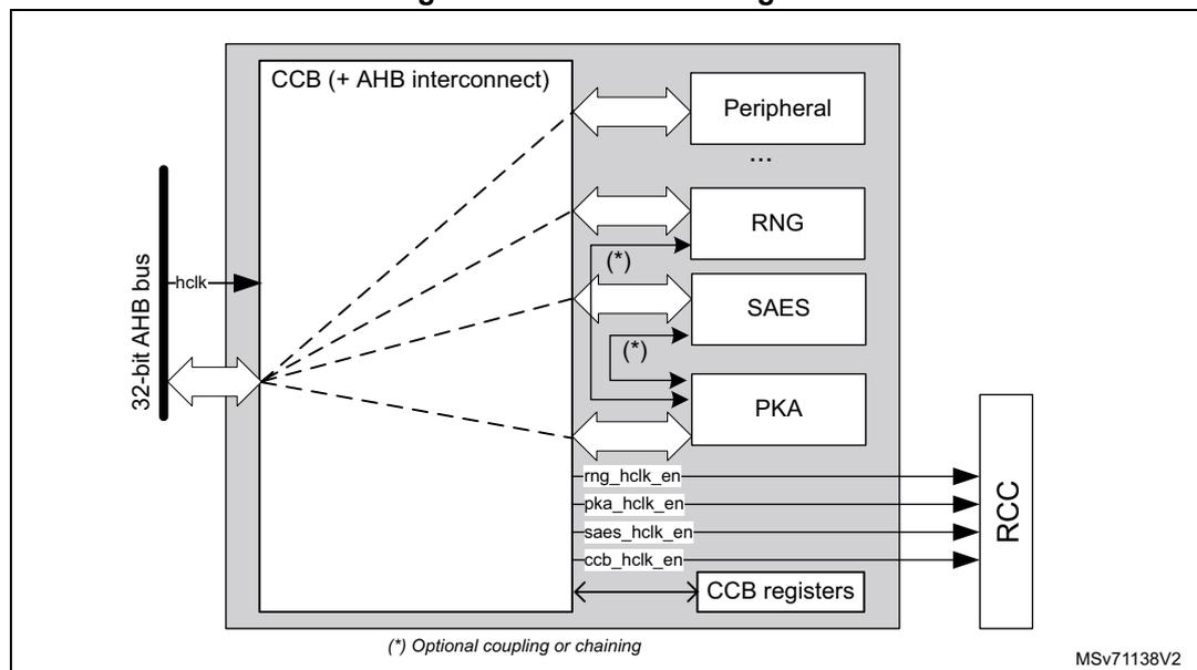
31.4.2 CCB internal signals
Table 286 describes the relevant internal signals interfacing the CCB peripheral. Signals targeting peripherals connected to the CCB are not listed.
Table 286. CCB internal input/output signals
| Signal name | Signal type | Description |
|---|---|---|
| hclk | Digital input | Interconnect system clock input |
| ccb_hclk_en | Digital output | CCB clock request to the RCC |
| x_hclk_en | Digital output | Peripheral x clock request to the RCC (x = SAES, PKA, or RNG) |
31.4.3 CCB reset and clocks
The CCB shares the same clock used by the AHB bus. Once the CCB clock is activated in the RCC, and coupling and chaining activity is activated by setting
\(
CCOP \neq 0
\)
in
CCB_CR
, the CCB automatically requests the RCC to enable RNG, SAES, and PKA clocks. These clocks remain enabled until the application gates them in the RCC, with
\(
CCOP
\)
cleared in the
CCB_CR
register.
The CCB has a dedicated reset bit in the RCC, and a system reset input. Locally to the CCB it is also possible to trigger a reset of the peripheral based on IPRST (do not use it when the application does not use CCB) in the
CCB_CR
register (refer to the bitfield description for details). Status register
CCB_SR
has a specific reset behavior (see
Section 31.7.2
).
When at least a cryptographic peripheral raises a tamper event, the CCB requests its clock to the RCC. The tamper status
TAMP_EVTi
of these peripherals can be found in the
CCB_SR
register, as defined in
Section 31.3
.
31.4.4 CCB coupling and chaining
Note: The selection of these chaining modes is defined in Section 31.5 . In most of these operations, a read of the PKA RAM returns 0 (shown with a purple circle in the following figures).
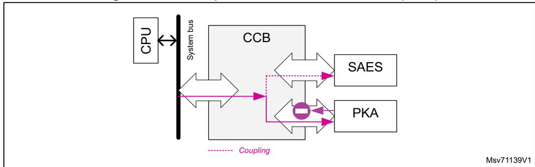
Coupling CPU → PKA + SAES (write)
When the corresponding OPSTEP is selected, the CCB takes the write requests that go to the PKA RAM, and sends them to
SAES_DINR
, as shown in
Figure 304
. Write to
SAES_DINR
is not coupled to the PKA. The CCB sends both data and address to
SAES_DINR
.
Figure 304. CCB operation CPU → PKA + SAES (write)
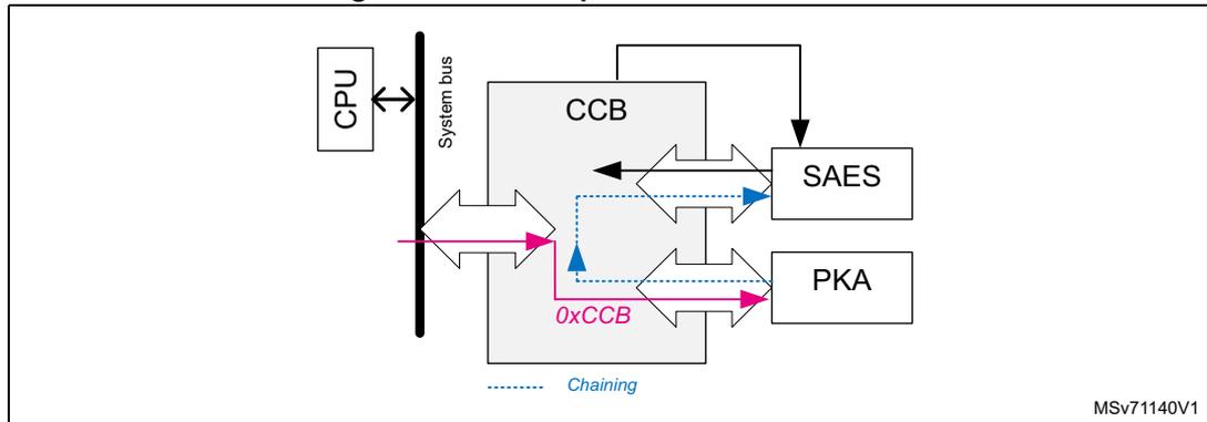
Chaining PKA → SAES
When the corresponding OPSTEP is selected, for each 32-bit write request to the PKA RAM of magic number 0xCCB, the CCB generates a read request from the write target (in the PKA RAM) to SAES_DINR.
Figure 305. CCB operation PKA → SAES
Chaining SAES → PKA
When the corresponding OPSTEP is selected, the CCB takes the write requests that go to the PKA RAM, and substitutes these data by a 32-bit word coming from SAES_DOU TR. When available, this chaining is activated when the application writes 0xCCB to PKA RAM.
Figure 306. CCB operation SAES → PKA

Chaining SAES → CCB
When the corresponding OPSTEP is selected, the CCB takes the read requests to SAES_DOUTR, and sends them to the system interconnect and to CCB_REFTAGRx holding the reference TAG information. For confidentiality reason, read data toward system bus are zeroed by the CCB.
If the CCB finds that the transferred value matches its reference information, it signals to the PKA that it can proceed with the protected PKA operation (START bit can be set).
Figure 307. CCB operation SAES → CCB
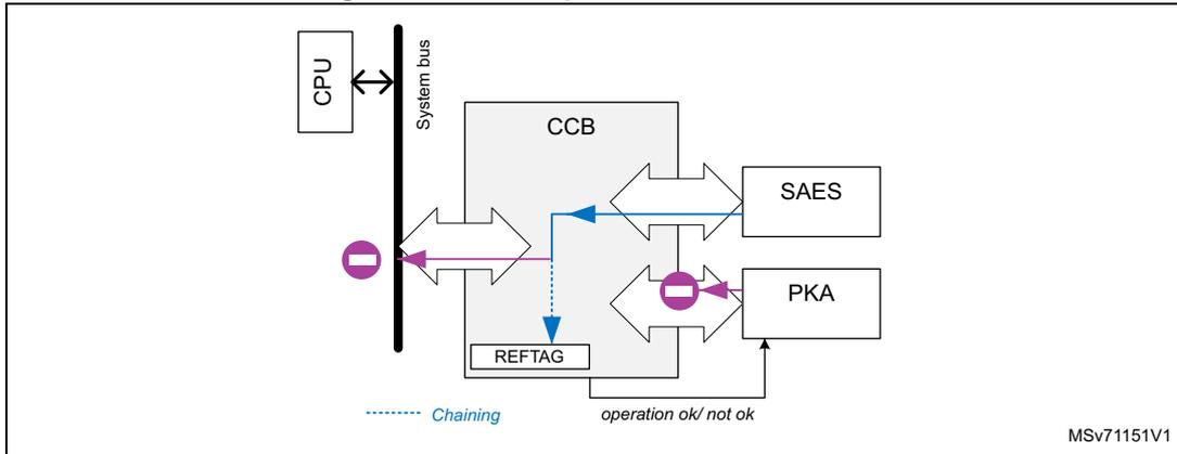
The diagram illustrates the data flow for the SAES → CCB chaining operation. A CPU is connected to a System bus. The System bus is connected to the CCB. The CCB is connected to SAES and PKA. A REFTAG block is also connected to the CCB. A dashed blue arrow labeled 'Chaining' points from the CCB to the PKA. A solid blue arrow points from the SAES to the CCB. A solid purple arrow points from the CCB to the PKA, labeled 'operation ok/ not ok'. A solid purple arrow points from the CCB to the REFTAG. A solid purple arrow points from the REFTAG to the CCB. A solid purple arrow points from the CCB to the System bus, labeled with a minus sign in a circle. The diagram is labeled MSv71151V1.
Chaining RNG → PKA (write)
When the corresponding OPSTEP is selected, the CCB takes the write requests that go to the PKA RAM, and substitutes these data with random numbers coming from RNG_DR. For consistency, the application can write 0xCCB to activate this chaining.
Figure 308. CCB operation RNG → PKA (write)
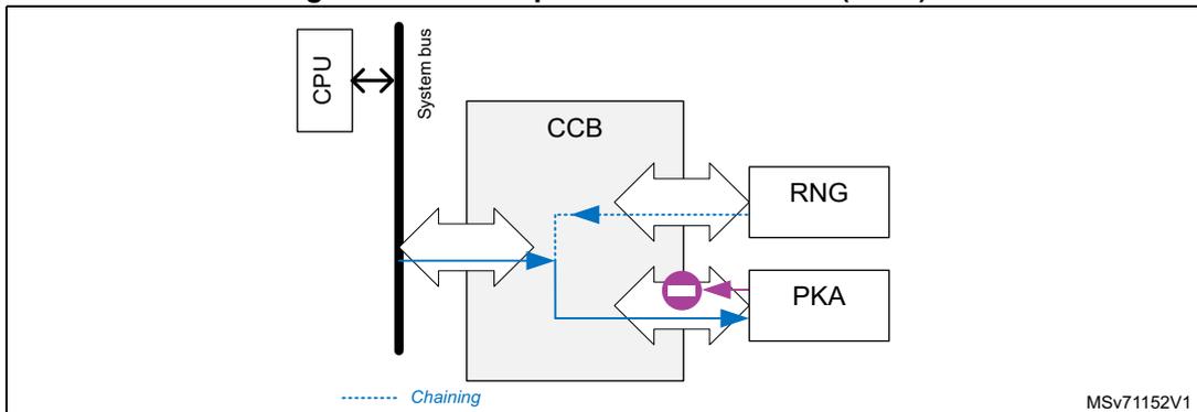
The diagram illustrates the data flow for the RNG → PKA (write) chaining operation. A CPU is connected to a System bus. The System bus is connected to the CCB. The CCB is connected to RNG and PKA. A dashed blue arrow labeled 'Chaining' points from the CCB to the PKA. A solid blue arrow points from the RNG to the CCB. A solid blue arrow points from the CCB to the PKA. A solid purple arrow points from the CCB to the PKA, labeled with a minus sign in a circle. The diagram is labeled MSv71152V1.
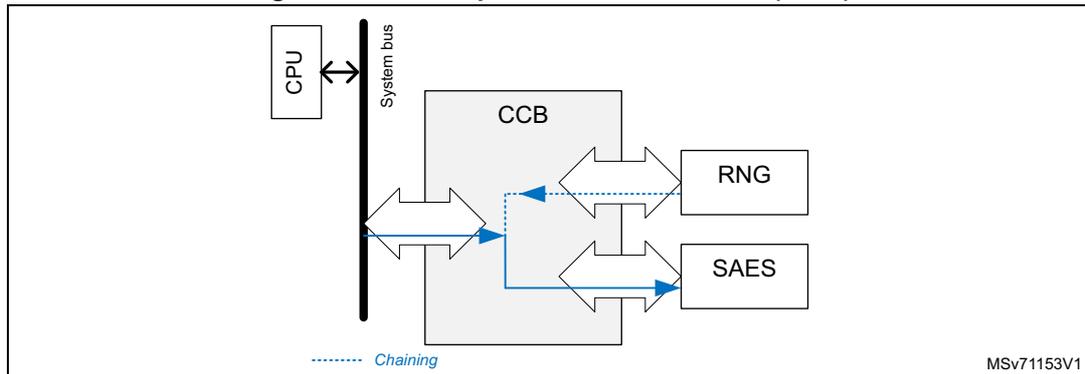
Chaining RNG → SAES (write)
When the corresponding OPSTEP is selected, the CCB takes the write requests that go to SAES_IVR1 to IVR3, and substitutes these data with random numbers coming from RNG_DR. For consistency, the application can write 0xCCB to activate this chaining.
Figure 309. CCB operation RNG → SAES (write)
31.4.5 CCB error management
When the CCB detects an error during a coupling and chaining operation (see Section 31.5 ), it sets accordingly OPERR[5:0] in CCB_SR (see Section 31.7.2 for the possible errors).
When OPERR[5:0] \( \neq \) 0 in CCB_SR, the CCB raises IPRST in CCB_CR, sets OPSTEP[4:0] to 0x1F, and sets CCB_BUSY bit to 1. The application must clear IPRST to be able to use again the CCB and the peripheral(s) used by the coupling and chaining operation.
31.5 CCB coupling and chaining operations
When an application must enforce private key confidentiality by wrapping them with a 256-bit hardware unique key, the following steps are needed:
- 1. Select the protected operation in the PKA that uses this private key (ECDSA signature, scalar multiplication, modular exponentiation). Then, choose the CCOP value in the CCB that corresponds to the selected operation, as defined in this section. Then, as multiple cryptographic peripherals are used, make sure to follow the guidelines described in Section 31.5.1
- 2. When CCB is active (OPSTEP=0x1), select in the SAES the DHUK (with optional XOR with BHK), or unwrap in the SAES an existing blob encryption key that has been encrypted (in wrapped-key mode) using the DHUK. A 256-bit KEYSIZE must be selected.
As the DHUK value is different when CCB is active or inactive, the operation of wrapping or unwrapping blob encryption key in SAES (with KMOD[1:0]=0x1) must be done when OPSTEP=0x1. Refer to operation with wrapped keys in Section 34: Secure AES coprocessor (SAES) for details.
- 3. When the application uses this protected operation in the PKA, it must load the related blob information in the PKA RAM and in SAES_DINR.
- – If the information exactly matches the conditions of the blob generation (choice and order of the writes of protected parameters in the PKA RAM, selection of blob
- encryption key, use of original encrypted secrets), the CCB allows the application to set START bit in PKA_CR.
- – If the blob information does not match the conditions of the blob generation, the application can only reset the sequence by setting IPRST bit in CCB_CR. CCB, PKA, and SAES become available when CCB_BUSY is cleared in CCB_SR.
- 4. At any time, the application can abort the executing protected operation by using the IPRST bit in CCB_CR.
- 5. When creating a blob, always use it once before trusting it to be stored in non-volatile memory or given to a less trusted code (see
Figure 310
). More specifically, each time a blob is created:
- – For ECDSA signature blob: use it to compute the public key, and use this key to verify the signature computed during the blob creation.
- – For ECC key blob: use it to compute the public key, and verify key coordinates match those of the key computed during the blob creation.
- – For RSA key blob: use it to compute a reference modular exponentiation and verify it matches the one computed during the blob creation.
Figure 310. Blob creation scenarios
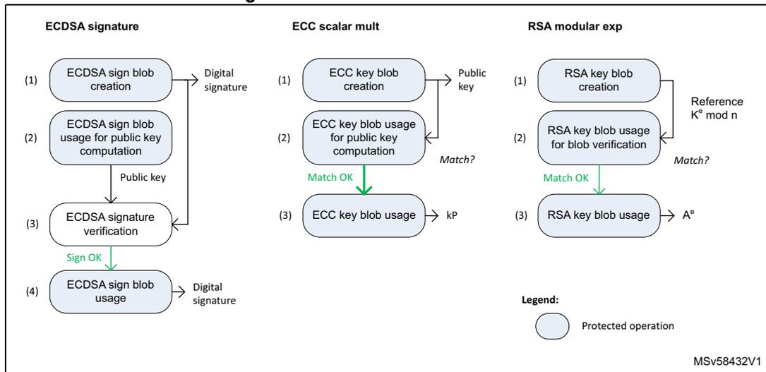
The diagram illustrates three blob creation scenarios: ECDSA signature, ECC scalar mult, and RSA modular exp. Each scenario consists of a sequence of steps, some of which are protected operations (indicated by light blue rounded rectangles).
- ECDSA signature:
- (1) ECDSA sign blob creation (Protected operation) → Digital signature
- (2) ECDSA sign blob usage for public key computation (Protected operation) → Public key
- (3) ECDSA signature verification (Protected operation) → Sign OK
- (4) ECDSA sign blob usage → Digital signature
- ECC scalar mult:
- (1) ECC key blob creation (Protected operation) → Public key
- (2) ECC key blob usage for public key computation (Protected operation) → Match?
- (3) ECC key blob usage (Protected operation) → kP
- RSA modular exp:
- (1) RSA key blob creation (Protected operation) → Reference \( K^e \bmod n \)
- (2) RSA key blob usage for blob verification (Protected operation) → Match?
- (3) RSA key blob usage (Protected operation) → \( A^e \)
Legend:
(Light blue rounded rectangle) Protected operation
MSV58432V1
This section describes how to do the above steps, for all available protected operations in the PKA. Note that:
- • Bold elements in the following tables are key inputs that the application must save in non-volatile memory after the newly created blob has been confirmed by its first usage.
- • The CCB automatically goes to the next step, updating the OPSTEP value, when the application clears or performs the end-step event described in tables of Section 31.5.2 to Section 31.5.4 .
- • When an incremental read or write is mentioned, the application must write four bytes in the PKA memory, with an incremental memory address (modulo 0x8). Otherwise, the CMF error flag is triggered, and the process must be restarted.
- • When writing to SAES_CR register the application must write the configuration expected by the CCB, otherwise an OPERR might be raised. Refer to the OPSTEP “CPU action” instructions in the application tables ( Table 287 through Table 293 ).
- • When the CCB uses the RNG, the application must check in RNG_SR that no error occurred (SEIS = CEIS = 0), and that a random number is ready (DRDY = 1). In case of issue, RNGOKF is not set, and the application must ensure that the RNG is functional before running again the OPSTEP sequence that uses the RNG.
- • For each OPSTEP>0, the application must manage the error flags that could occur in the RNG, SAES or PKA blocks. During a normal protected operation, no error flags are expected. Refer to Section 31.4.5: CCB error management for details on CCB error management.
- • When CCB draws random number to compute ECC private keys, it implements the testing candidates method defined by NIST in FIPS PUB 186-4 section B.4.
Note: It is not possible to generate RSA key pairs with the CCB, they must be generated outside the device.
31.5.1 Preliminary steps before any protected operation
The following steps are required before running any operation described in this section:
- 1. Initialize the GTZC using the same security/privilege configuration protections for the SAES, PKA, RNG and CCB peripherals (see Section 5: Global TrustZone controller (GTZC) ). Otherwise OPERR=0x1A occurs (see Section 31.7.2 ).
- 2. Activate both RNG clocks, then initialize the peripheral to be fully functional, without pending errors.
- 3. Activate the PKA clock, then release the PKA reset. The PKA is functional once its RAM is automatically erased, and it has fetched the necessary random numbers. For further details refer to enabling/disabling PKA in Section 36: Public key accelerator (PKA) .
- 4. Activate the SAES clock, then release the SAES reset. The SAES is functional once it has fetched necessary random numbers.
- 5. Activate the CCB clock, set IPRST bit in CCB_CR, then clear it when CCB_BUSY=0x0 in CCB_SR.
Note: Step 4 can be done before step 3, as CCOP = 0x0.
31.5.2 ECDSA signature
This PKA operation is protected against side-channel attacks. When CCOP = 0x0, all parameters loaded in the PKA RAM are managed in the clear by the application. When CCOP = 0xC3, the private key \( d \) can be manipulated by the application only if encrypted, using a special blob called “ECDSA signature blob”.
ECDSA signature blob creation
The ECDSA signing operation is prepared by generating and then encrypting the private key d , and computing the reference GCM tag. This process is summarized Table 287 , with coupling and chaining operations described in Section 31.4.4 . This sequence starts by setting CCOP to 0xC0 or 0xC2 in CCB_CR.
Table 287. Blob creation steps for ECDSA signature (CCOP = 0b110000<i>0)
| OP STEP | MODE in PKA | GCM PH in SAES | Coupling or chaining | End-step event (1) | CPU action in the step |
|---|---|---|---|---|---|
| 0x1 | N/A | N/A | N/A | AES GCM selected, GCMPH = 0x0 |
|
| 0x2 | 0x0 | RNG -> SAES | GCMPH = 0x1 (following GCM initialization) |
| |
| 0x3 | 0x24 | 0x1 | CPU -> PKA + SAES | GCMPH = 0x2 | Write ECC signature parameters in the PKA RAM, clearing CCF flags in the SAES triggered after each 2x32-bit write. |
| 0x6 (<i>=1) | 0x24 | 0x2 | RNG -> PKA | RNGOKF set | Write incrementally d in the PKA, using 0xCCB magic number. Values are drawn from the RNG. The PKA runs a special sanity check to verify random compliance with NIST standard (RNGERRF is set if sanity check fails). |
| 0x4 (<i>=0) | n/a | DATAOKF set | Write incrementally d in the PKA. | ||
| 0x8 | PKA -> SAES | DATAOKF set |
| ||
| 0x9 | 0x24 | RNG -> PKA | RNGOKF set, GCMPH = 0x3 |
| |
| 0xA (2) | 0x3 | N/A | START= 0x1 |
|
Table 287. Blob creation steps for ECDSA signature (CCOP = 0b110000<i>0) (continued)
| OP STEP | MODE in PKA | GCM PH in SAES | Coupling or chaining | End-step event (1) | CPU action in the step |
|---|---|---|---|---|---|
| 0x19 (3) | N/A | N/A | PROCENDF set | The PKA computes the operation, PKA RAM reads as 0 | |
| 0x1A | 0x24 | N/A | N/A | IPRST set in the CCB |
|
| 0x0 | N/A | N/A | N/A | N/A |
|
- 1. The application must clear and/or perform the described event for the CCB to automatically go to the next step.
- 2. Once START bit is set SAES is reset, and OPERR linked to SAES are deactivated. Also when START bit is set, CCB sets OPSTEP to 0x19 after a few cycles.
- 3. SAES cannot be used for any operations, for security reasons.
The sequence described in Table 287 is detailed below. Refer to the table for OPSTEP values and related coupling/chaining modes.
- 1. Write CCOP = 0xC0 or 0xC2 in CCB_CR.
- 2. Enable the PKA in the correct mode, writing in PKA_CR MODE=0x24 and EN=1 (repeat if the EN bit stays clear). Wait for INITOK=1 in PKA_SR.
- 3. Write the hash of the message in the PKA RAM
- 4. Initialize the ECC signature blob key in the SAES. This key can be the DHUK (KEYSEL = 0x1 or 0x4), or a key decrypted in 256-bit wrapped key mode by the DHUK (KEYSEL = 0x1 or 0x4, KMOD = 0x1, MODE = 0x1 or 0x2). See Section 34: Secure AES coprocessor (SAES) for details.
- 5. In the SAES, set the GCM chaining mode in encryption mode (CHMOD = 0x3, GCM PH = 0x0, MODE = 0x0, DATATYPE = 0x0). Then:
- a) Configure the 256-bit key size using KEYSIZE.
- b) Write SAES_IVRx, with any value (except SAES_IVR0 that must be equal to 0x2). For SAES_IV1 to IV3, random values are loaded into the SAES by the CCB. If an error occurs, RNGERRF is set in CCB_SR.
- c) Read back SAES_IVR1 to SAES_IVR3, and save the value in non-volatile memory after blob verification.
- d) Set EN in SAES_CR, and wait until CCF = 1 in SAES_ISR (end of GCM init).
- e) Clear CCF flag in SAES_ICR.
- 6. Select the header phase of the running GCM chaining mode (GCM PH = 0x1). Write the protected operation (ECDSA signature) mandatory parameters in the PKA RAM, as described in
Section 36: Public key accelerator (PKA)
. Do the following when writing data in the PKA:
- a) Write two 32-bit word in the PKA RAM, then wait until CCF is set in SAES_ISR. An SAES interrupt can be triggered when this flag is set.
- b) Clear CCF in SAES_ICR.
- 7. Select the payload phase of the running GCM chaining mode (GCM
PH
= 0x2). Write the private key
d
in the PKA RAM using the following sequence:
- a) If CCOP = 0xC0, write the private key d value in the PKA RAM. If CCOP = 0xC2, write the 32-bit magic number 0xCCB to the private key d parameter addresses in the PKA memory. The CCB then draws the value of d from the RNG, with PKA running a special sanity check to verify random compliance with NIST standard.
- b) Complete parameter information with the mandatory two 32-bit zeroed words. At the end of this process, the private key d of size d_size is written in the PKA RAM. Clear the error flag, then restart step 6 if the PKA sets RNGERRF when BUSY is cleared.
- 8. When the PKA sets its completion flag (RNGOKF if CCOP = 0xC2, DATAOKF if CCOP = 0xC0), clear it, then read the private key
d
in the PKA RAM using the sequence below (starting from the LSB word in the PKA RAM, and increasing the addresses modulo 0x8):
- a) For each 64-bit word in the PKA RAM, write twice the 32-bit magic number 0xCCB to the private key d parameter addresses in the PKA memory. The target content of the PKA memory is transferred to SAES_DINR by the CCB. Wait until CCF is set in SAES_ISR (end of AES encryption). An SAES interrupt can be triggered when this flag is set.
- b) Clear CCF flag in SAES_ICR. Then read the encrypted private key d in SAES_DOUT, to save it in the non-volatile memory after blob verification.
- c) For the final 64-bit word (mandatory zeroed word): if the d_size is proportional to 16 bytes (for example, for 192- and 521-bit curves), the final 64 bits must be written to with two 32-bit magic numbers 0xCCB. If the d_size is not proportional to 16 bytes (for example, for 256- and 512-bit curves), the final 64 bits must be written with 0s.
- 9. When DATAOKF = 1 in PKA_SR (private key d ok), clear this flag. Then write to the integer k parameter addresses in the PKA memory, starting from the LSB word in the PKA RAM, and increasing the addresses modulo 0x8. The CCB draws the value of k from the RNG. The PKA then runs a special sanity check to verify random compliance with NIST standard. Clear the error flag then restart this step if the PKA sets RNGERRF when BUSY is cleared.
- 10. When RNGOKF = 1 in PKA_SR (random k OK), clear this flag. Then select the final phase of the running GCM chaining mode (GCM PH = 0x3). Write the last GCM block in SAES_DINR. Then wait until CCF is set in SAES_ISR (end of GCM final).
- 11. Read SAES_DOUTR four times to retrieve the ECDSA signature blob reference tag. Save it in the non-volatile memory after blob verification. Do not disable SAES by clearing the EN bit.
- 12. Set START bit in PKA_CR to run the ECDSA signature operation.
- 13. When the PROCENDF completion flag is set save the ECDSA signature ( r,s ) of the hash z in SRAM to use it after using the new blob for public-key computation.
- 14. Clear CCOP by setting IPRST bit in CCB_CR. After CCB_BUSY is cleared in CCB_SR, clear the IPRST bit. The SAES, and PKA can again be used for any tasks. They are unprotected by the CCB until CCOP is written different from 0.
ECCSA signature blob usage for ECCSA signature
Table 288 summarizes the ECCSA signing operation using the encrypted private key d, the reference blob IV, and the computed GCM tag of Table 287 . Coupling and chaining traffic options are described in Section 31.4.4 . This sequence starts by setting CCOP to 0xC3 in the CCB_CR register.
Table 288. Blob use steps for ECCSA signature (CCOP = 0b11000011)
| OPSTEP | MODE in PKA | GCMPH | Coupling or chaining operations | End-step event (1) | CPU action in step |
|---|---|---|---|---|---|
| 0x1 | N/A | N/A | N/A | AES GCM selected, GCMPH = 0x0 |
|
| 0x12 | 0x0 | N/A | GCMPH = 0x1 (following GCM initialization) |
| |
| 0x13 | 0x1 | CPU -> PKA + SAES | GCMPH = 0x2 | Write ECC signature parameters in the PKA RAM, clearing CCF flags in the SAES, triggered after each 64-bit write. | |
| 0x14 | 0x24 | 0x2 | SAES -> PKA | DATAOKF set |
|
| 0x16 | RNG -> PKA | RNGOKF set, GCMPH = 0x3 | Write incrementally k in the PKA, using 0xCCB magic number. Values are drawn from the RNG. The PKA runs a special sanity check to verify random compliance with NIST standard (RNGERRF is set if the sanity check fails). | ||
| 0x17 | 0x3 | SAES -> CCB | Tag matches REFTAGR? |
| |
| 0x18 | N/A | N/A | START = 0x1 | Start the operation in PKA setting START bit in PKA_CR. | |
| 0x19 (2) | 0x24 | N/A | N/A | PROCENDF set | The PKA computes the operation, PKA RAM is read as 0. |
| 0x1A | N/A | N/A | N/A | Read signature (r,s) in the PKA RAM. |
1. The application must clear and/or perform the described event for the CCB to automatically go to the next step.
2. SAES cannot be used for any operations, for security reasons..
The sequence described in Table 288 is detailed below. Refer to the table for the OPSTEP values and related coupling and chaining modes.
- 1. Write CCOP = 0xC3 in CCB_CR.
- 2. Enable the PKA in the correct mode, writing in PKA_CR MODE=0x24 and EN=1(repeat if the EN bit stays clear). Wait for INITOK=1 in PKA_SR.
- 3. Write the hash of the message in the PKA RAM.
- 4. Initialize the ECC signature blob key in the SAES. This key can be the DHUK (KEYSEL = 0x1 or 0x4), or a key decrypted in 256-bit wrapped key mode by the DHUK (KEYSEL = 0x1 or 0x4, KMOD = 0x1, MODE = 0x1). Refer to Section 34: Secure AES coprocessor (SAES) for details.
- 5. Set the GCM chaining mode in decryption in the SAES (CHMOD = 0x3, GCMPH = 0x0, MODE = 0x2, DATATYPE = 0x0). Then:
- a) Configure the 256-bit key size using KEYSIZE.
- b) Write to SAES_IVRx registers the value saved in non-volatile memory.
- c) Set EN in SAES_CR, and wait until CCF is set in SAES_ISR (end of GCM init).
- d) Clear CCF flag in SAES_ICR.
- e) Write to CCB_REFTAGR registers, the ECDSA signature blob reference tag value saved in non-volatile memory.
- 6. Select the header phase of the running GCM chaining mode (GCMPH = 0x1). Write the protected operation (ECDSA signature) mandatory parameters in the PKA RAM, exactly as done during the blob creation. See step 5 in ECDSA signature blob creation for details.
- 7. Select the payload phase of the running GCM chaining mode (GCMPH = 0x2). Write the protected private key d in the PKA RAM, following the below sequence (starting from the LSB word in the PKA RAM, and increasing the addresses modulo 0x8):
- a) Write two 64-bit words of encrypted private key d in SAES_DINR. Wait until CCF is set in SAES_ISR (end of AES decryption). An SAES interrupt can be triggered when this flag is set.
- b) Clear the CCF flag in the SAES_ICR register. Then, for both 64-bit words, write four times the 32-bit magic number 0xCCB to the private key d parameter addresses in the PKA memory. The CCB transfers the clear-text content of SAES_DOUTr to the PKA.
- c) For the final 64-bit word (mandatory zeroed word): If d_size defined in step 6 in ECDSA signature blob creation is not proportional to 16-bytes (for example, for 256- and 512-bit curves), the final 64 bits must be written with 0s.
- 8. When DATAOKF = 1 in PKA_SR (private key d ok), clear this flag. Then write to the integer k parameter addresses in the PKA memory, starting from the LSB word in the PKA RAM, and increasing the addresses modulo 0x8. The CCB draws the value of k from the RNG. The PKA then runs a special sanity check to verify random compliance with NIST standard. Clear the error flag, then restart step 7 if the PKA sets RNGERRF when BUSY is cleared.
- 9. When RNGOKF = 1 in PKA_SR (random k ok), clear this flag. Then select the final phase of the running GCM chaining mode (GCMPH = 0x3). Write the last GCM block in SAES_DINR. Then wait until CCF is set in SAES_ISR (end of GCM final).
- 10. Read four times SAES_DOUTr (returns 0s). If PKA parameters were written exactly like during the blob creation, and the correct private key d was used, and all expected DATAOKF/RNGOKF flags were raised then cleared, the application can set START bit
in PKA_CR to run the ECDSA signature operation. Otherwise, IPRST in CCB_CR must be used to restart the sequence from step 1.
- Clear CCOP by setting IPRST in CCB_CR. After CCB_BUSY is cleared in CCB_SR, clear the IPRST bit. The SAES, and PKA can again be used for any tasks. They are unprotected by the CCB until CCOP in CCB_CR is written different from 0.
ECDSA signature blob use for public-key computation
The ECC public key computation using the encrypted private key d, the reference blob IV, and the computed GCM tag of Table 287 is summarized in Table 289 . The additional ECDSA verification at the end of the sequence must be used before saving a new ECDSA signature blob in non-volatile memory. Shown coupling and chaining traffic options are described in Section 31.4.4 . This sequence starts by setting CCOP to 0x81 in the CCB_CR register.
Table 289. Blob use steps for signing public key computation (CCOP = 0b10000001)
| OPSTEP | MODE in PKA | GCMPH in SAES | Coupling or chaining operations | End-step event (1) | CPU action |
|---|---|---|---|---|---|
| 0x1 | N/A | N/A | N/A | AES GCM selected, GCMPH = 0x0 |
|
| 0x12 | 0x0 | N/A | GCMPH = 0x1 (following GCM initialization) |
| |
| 0x13 | 0x1 | CPU -> PKA + SAES | GCMPH = 0x2 | Write ECC signature parameters in the PKA RAM, clearing CCF flags in SAES, triggered after each 2x32-bit write. | |
| 0x14 | 0x20 | 0x2 | SAES -> PKA | DATAOKF set, GCMPH = 0x3 |
|
| 0x17 | 0x3 | SAES -> CCB | Tag matches REFTAGR? |
| |
| 0x18 | N/A | N/A | START = 0x1 | Start the operation in PKA setting START bit in PKA_CR. | |
| 0x19 (2) | 0x20 | N/A | N/A | PROCENDF set | The PKA computes the operation. PKA RAM is read as 0. |
| 0x1A | 0x20 | N/A | N/A | N/A | – Read public key point Q in PKA RAM |
| OPSTEP | MODE in PKA | GCMPH in SAES | Coupling or chaining operations | End-step event (1) | CPU action |
|---|---|---|---|---|---|
| 0x1A | 0x20 | N/A | N/A | IPRST set in the CCB |
|
| 0x0 | 0x26 | N/A | N/A | N/A | Clear the IPRST bit in CCB when CCB_BUSY and OPSTEP are cleared in CCB_SR. Before writing new ECDSA signature blob in non-volatile memory do the following:
|
- 1. The application must clear and/or perform described event for CCB to automatically go to the next step.
- 2. SAES cannot be used for any operations, for security reasons.
31.5.3 ECC scalar multiplication
This operation consists in the computation of \( k \times P \) , where \( P \) is a point on a curve over prime fields, and “ \( x \) ” is the elliptic curve scalar point multiplication. The computation result is a point that belongs to the same curve, or a point at infinity.
The scalar multiplication operation is protected against side-channel attacks. When CCOP = 0x0 in CCB_CR, all parameters loaded in the PKA RAM are managed in the clear by the application. When CCOP = 0x81, the scalar multiplier \( k \) can be manipulated by the application only if encrypted, using a special blob called “ECC key blob”.
Scalar multiplication “ECC key” blob creation
The scalar multiplication operation is prepared by generating then encrypting the scalar multiplier \( k \) , and computing the reference GCM tag. This process is summarized in Table 290 . Coupling and chaining operations described in Section 31.4.4 . This sequence starts by setting CCOP to 0x80 or 0x82 in CCB_CR register.
Table 290. Blob creation steps for scalar multiplication (CCOP = 0b100000<i>0)
| OPSTEP | MODE in PKA | GCMPH in SAES | Coupling or chaining operations | End-step event (1) | CPU action in step |
|---|---|---|---|---|---|
| 0x1 | N/A | N/A | N/A | AES GCM selected, GCMPH = 0x0 |
|
| 0x2 | 0x0 | RNG → SAES | GCMPH = 0x1 (following GCM initialization) |
| |
| 0x3 | 0x20 | 0x1 | CPU → PKA + SAES | GCMPH = 0x2 | Write ECC scalar multiplication parameters in the PKA RAM, clearing CCF flags in SAES, triggered after each 64-bit write. |
| 0x6 (<i>=1) | 0x20 | 0x2 | RNG → PKA | RNGOKF set | Write incrementally k in the PKA, using 0xCCB magic number. Values are drawn from the RNG. The PKA runs a special sanity check to verify random compliance with NIST standard (RNGERRF is set if the sanity check fails). |
| 0x4 (<i>=0) | N/A | DATAOKF set | Write incrementally k in the PKA. | ||
| 0x8 | 0x20 | 0x2 | PKA → SAES | DATAOKF set, GCMPH = 0x3 |
|
| 0xA (2) | 0x3 | N/A | START= 0x1 |
| |
| 0x19 (3) | 0x20 | N/A | N/A | PROCENDF set | The PKA computes the operation, PKA RAM reads as 0 |
| 0x1A | N/A | N/A | IPRST set in the CCB |
| |
| 0x0 | N/A | N/A | N/A | N/A | Clear the IPRST bit in CCB when CCB_BUSY and OPSTEP are cleared in CCB_SR. |
1. The application must clear and/or perform described event for CCB to automatically go to the next step.
2. Once START bit is set SAES is reset, and OPERR linked to SAES are deactivated. Also when START bit is set, CCB sets OPSTEP to 0x19 after a few cycles.
3. SAES cannot be used for any operations, for security reasons.
Scalar multiplication blob use for example for ECC decryption
ECC scalar multiplication computation using the encrypted k, the reference blob IV and the computed GCM tag of Table 290 is summarized in Table 291 . Shown coupling and chaining traffic options are described in Section 31.4.4 . This sequence starts by setting CCOP to 0x81 in CCB_CR register.
Table 291. Blob use steps for scalar multiplication (CCOP = 0b10000001)
| OPSTEP | MODE in PKA | GCM PH in SAES | Coupling or chaining operations | End-step event (1) | CPU action |
|---|---|---|---|---|---|
| 0x1 | N/A | N/A | N/A | AES GCM selected, GCM PH = 0x0 |
|
| 0x12 | 0x0 | N/A | GCM PH = 0x1 (following GCM initialization) |
| |
| 0x13 | 0x1 | CPU -> PKA + SAES | GCM PH = 0x2 | Write ECC scalar multiplication parameters in the PKA RAM, clearing CCF flags in the SAES, triggered after each 64-bit write. | |
| 0x14 | 0x20 | 0x2 | SAES -> PKA | DATAOKF set, GCM PH = 0x3 |
|
| 0x17 | 0x3 | N/A | Tag matches REFTAGR? |
| |
| 0x18 | START = 0x1 | Start the operation in PKA setting START bit in PKA_CR. Do not use SAES during this step (under reset). | |||
| 0x19 (2) | 0x20 | N/A | N/A | PROCENDF set | The PKA computes the operation. The PKA RAM is read as 0. |
| 0x1A | N/A | Read kP point coordinates in the PKA RAM. If this point is the public key verify it matches the reference public key computed in Table 290 before saving the created blob in non-volatile memory. |
1. The application must clear and/or perform described event for CCB to automatically go to the next step.
2. SAES cannot be used for any operations, for security reasons.
31.5.4 RSA modular exponentiation
The modular exponentiation operation is commonly used to perform a single-step RSA operation. It consists in the computation of \( A^e \bmod n \) .
This modular exponentiation operation (MODE = 0x3) is protected against side-channel attacks. When CCOP = 0x0, all parameters loaded in the PKA RAM are managed in the clear by the application. When CCOP = 0x45, the exponent \( e \) and phi value can only be manipulated encrypted by application, using a special blob called “RSA key blob”.
Modular exponentiation “RSA key” blob creation
Modular exponentiation operation is prepared by generating then encrypting the scalar multiplier \( k \) and computing the reference GCM tag. This process is summarized in Table 292 . The coupling and chaining operations described in Section 31.4.4 . This sequence starts by setting CCOP to 0x44 in CCB_CR register.
Table 292. Blob creation steps for modular exponentiation (CCOP = 0b01000100)
| OPSTEP | MODE in PKA | GCM PH in SAES | Coupling or chaining operations | End-step event (1) | CPU action in step |
|---|---|---|---|---|---|
| 0x1 | N/A | N/A | N/A | AES GCM selected, GCM PH = 0x0 |
|
| 0x2 | 0x0 | RNG -> SAES | GCM PH = 0x1 (following GCM initialization) |
| |
| 0x3 | 0x03 | 0x1 | CPU -> PKA + SAES | GCM PH = 0x2 | Write protected modular exponentiation parameters (PKA mode 0x3) in the PKA RAM, clearing CCF flags in the SAES triggered after each 2x32-bit write. |
| 0x4 | 0x3 | 0x2 | N/A | DATAOKF set | Write incrementally clear-text exponent \( e \) . |
| 0x5 | DATAOKF set | Write incrementally clear-text phi. | |||
| 0x8 | 0x3 | 0x2 | PKA -> SAES | DATAOKF set |
|
| 0x9 | DATAOKF set, GCM PH = 0x3 |
| |||
| 0xA (2) | 0x3 | 0x3 | N/A | START= 0x1 |
|
| OPSTEP | MODE in PKA | GCMPH in SAES | Coupling or chaining operations | End-step event (1) | CPU action in step |
|---|---|---|---|---|---|
| 0x19 (3) | 0x3 | N/A | N/A | PROCENDF set | The PKA computes the operation, PKA RAM is read as 0 |
| 0x1A | N/A | N/A | IPRST set in the CCB | – Read the reference modular exponentiation
\(
K^e \bmod n
\)
in PKA RAM, and save it in SRAM to verify the new blob. – Set IPRST in CCB | |
| 0x0 | N/A | N/A | N/A | N/A | Clear the IPRST bit in CCB when CCB_BUSY and OPSTEP are cleared in CCB_SR. |
- 1. The application must clear and/or perform described event for CCB to automatically go to the next step.
- 2. Once START bit is set SAES is reset, and OPERR linked to SAES are deactivated. Also when START bit is set, CCB sets OPSTEP to 0x19 after a few cycles.
- 3. SAES cannot be used for any operations, for security reasons.
Modular exponentiation blob use (for example for RSA decryption)
The modular exponentiation computation using the encrypted \( e \) and \( \phi \) , the reference blob IV, and the computed GCM tag of Table 292 is summarized on Table 293 . Shown coupling and chaining traffic options are described in Section 31.4.4 . This sequence starts by setting CCOP to 0x45 in CCB_CR register.
Table 293. Blob use steps for modular exponentiation (CCOP = 0b01000101)| OPSTEP | MODE in PKA | GCMPH in SAES | Coupling or chaining operations | End-step event (1) | CPU action |
|---|---|---|---|---|---|
| 0x1 | N/A | N/A | N/A | AES GCM selected, GCMPH = 0x0 | – Enable the PKA in the correct mode, writing in PKA_CR MODE= 0x3 and EN=1 (repeat if EN bit stays clear). Wait for INITOK=1 in PKA_SR. – Optionally decrypt blob encryption key in the SAES, using DHUK in 256-bit wrapped key mode. – Set up AES-GCM in decryption mode with DHUK or the decrypted key in register (if applicable). – Write operand A in the PKA RAM. Write constant K as operand A defined in Table 292 when verifying the created blob. |
Table 293. Blob use steps for modular exponentiation (CCOP = 0b010000101)
| OPSTEP | MODE in PKA | GCM PH in SAES | Coupling or chaining operations | End-step event (1) | CPU action |
|---|---|---|---|---|---|
| 0x12 | 0x0 | N/A | GCM PH = 0x1 (following GCM initialization) |
| |
| 0x13 | 0x03 | 0x1 | CPU -> PKA + SAES | GCM PH = 0x2 | Write protected modular exponentiation parameters (PKA mode 0x3) in the PKA RAM, clearing CCF flags in the SAES, triggered after each -bit write. |
| 0x14 | 0x2 | SAES -> PKA | DATAOKF set |
| |
| 0x15 | DATAOKF set, GCM PH = 0x3 |
| |||
| 0x17 | 0x3 | SAES -> CCB | Tag matches REFTAGR? |
| |
| 0x18 | 0x03 | N/A | N/A | START = 0x1 | Start the operation in PKA setting START bit in PKA_CR. |
| 0x19 (2) | PROCENDF set | The PKA computes the operation, PKA RAM is read as 0. | |||
| 0x1A | N/A | Read A e mod n in the PKA RAM. If the result is K e mod n verify it matches the reference computed in Table 292 before saving the created blob in non-volatile memory. |
- 1. The application must clear and/or perform described event for CCB to automatically go to the next step.
- 2. SAES cannot be used for any operations, for security reasons.
31.6 CCB interrupts
The CCB does not support any interrupt.
31.7 CCB registers
The following section provides information on registers.
Reserved bits (marked as Res.) must be kept at their reset values, unless otherwise specified.
For general information relative to register description, refer to Document conventions.
These registers are accessible through the AHB interface of the CCB (32-bit words only). All reads are supported. Writes accesses must be 32-bit word only (other access types generate an AHB error).
31.7.1 CCB control register (CCB_CR)
Address offset: 0x000
Reset value: 0x0000 0000
Following a CCB hardware reset, the above reset value applies if OPERR[5:0] = 0x0 and no TAMP_EVT bit is set.
| 31 | 30 | 29 | 28 | 27 | 26 | 25 | 24 | 23 | 22 | 21 | 20 | 19 | 18 | 17 | 16 |
|---|---|---|---|---|---|---|---|---|---|---|---|---|---|---|---|
| IPRST | Res. | Res. | Res. | Res. | Res. | Res. | Res. | Res. | Res. | Res. | Res. | Res. | Res. | Res. | Res. |
| rw | |||||||||||||||
| 15 | 14 | 13 | 12 | 11 | 10 | 9 | 8 | 7 | 6 | 5 | 4 | 3 | 2 | 1 | 0 |
| Res. | Res. | Res. | Res. | Res. | Res. | Res. | Res. | CCOP[7:0] | |||||||
| rw | rw | rw | rw | rw | rw | rw | rw | ||||||||
Bit 31 IPRST: CCB reset
Set this bit to start or abort any PKA protected operation defined in Section 31.5 . IPRST bit must be low while writing to any CCB register.
After setting this bit, the application must clear it when CCB_BUSY and OPSTEP are cleared in CCB_SR (IPRST clear is ignored otherwise). After this clear all CCB registers are read with their reset values. Setting IPRST clears any data stored in the SAES and the PKA.
When IPRST and CCB_BUSY are set, SAES registers are not accessible (read as 0, write ignored), and writes to EN and START bits in PKA_CR are ignored.
This bit is set by CCB when OPERR[5:0] ≠ 0 or any TAMP_EVT bit is set.
Bits 30:8 Reserved, must be kept at reset value.
Bits 7:0 CCOP[7:0] : Coupling and chaining operation
These bits must be set according to the chosen PKA protected operation (see Section 31.5 ).
0x044: Modular exponentiation blob creation with priv key from the CPU
0x045: Modular exponentiation blob use
0x080: ECC scalar multiplication blob creation with priv key from the CPU
0x082: ECC scalar multiplication blob creation with priv key from the RNG
0x081: ECC scalar multiplication blob use, or ECDSA signature blob use for public key computation
0x0C0: ECDSA signature blob creation with priv key from the CPU
0x0C2: ECDSA signature blob creation with priv key from the RNG
0x0C3: ECDSA signature blob use for ECDSA signature
Note: When an operation not listed here is written by the application, the write to CCOP[7:0] is ignored. All these operations implement protections against side-channel attacks. Write to CCOP is ignored when CCB_BUSY is set in CCB_SR.
31.7.2 CCB status register (CCB_SR)
Address offset: 0x004
Reset value: 0x0000 0000
This register is reset by a system reset, or after clearing IPRST in CCB_CR. The CCB reset input from the RCC has no effect on this register.
| 31 | 30 | 29 | 28 | 27 | 26 | 25 | 24 | 23 | 22 | 21 | 20 | 19 | 18 | 17 | 16 |
|---|---|---|---|---|---|---|---|---|---|---|---|---|---|---|---|
| Res. | Res. | TAMP_EVT5 | TAMP_EVT4 | TAMP_EVT3 | TAMP_EVT2 | TAMP_EVT1 | TAMP_EVT0 | Res. | Res. | Res. | Res. | Res. | Res. | Res. | CCB_BUSY |
| r | r | r | r | r | r | r | |||||||||
| 15 | 14 | 13 | 12 | 11 | 10 | 9 | 8 | 7 | 6 | 5 | 4 | 3 | 2 | 1 | 0 |
| Res. | Res. | OPERR[5:0] | Res. | Res. | Res. | OPSTEP[4:0] | |||||||||
| r | r | r | r | r | r | r | r | r | r | r | |||||
Bits 31:30 Reserved, must be kept at reset value.
Bits 29:24 TAMP_EVTi : Tamper i flag (i = 5 to 0)
0: No event
1: Tamper event i has been raised. Global tamper event is raised. See Section 31.3 for details on the events.
This bit is cleared by writing 0 to IPRST bit in CCB_CR. When at least one TAMP_EVT bit is set, CCB sets IPRST bit.
Bits 23:17 Reserved, must be kept at reset value.
Bit 16 CCB_BUSY : CCB busy
This flag is set when CCB is busy, or when OPSTEP[4:0] ≠ 0 following a CCB reset (hardware reset or use of IPRST in CCB_CR).
0: CCB idle
1: CCB busy or PKA RAM is being cleared following a peripheral reset.
When IPRST and CCB_BUSY are set, the SAES registers are not accessible (write ignored, read returns 0), and writes to EN or START bits in PKA_CR are ignored.
Bits 15:14 Reserved, must be kept at reset value.
Bits 13:8 OPERR[5:0] : Operation errorWhen an error is detected during a protected PKA operation, the CCB raises IPRST in CCB_CR, and OPSTEP[4:0] is set to 0x1F. The bitfield is cleared by setting IPRST to 0.
0x0: No error detected during protected PKA operation (if applicable)
0x1: CCB RCC reset has been detected when OPSTEP > 0x0
0x2: SAES RCC reset has been detected when OPSTEP > 0x0
0x3: PKA RCC reset has been detected when OPSTEP > 0x0
0x4: RNG RCC reset has been detected when OPSTEP > 0x0
0x5: The RCC has gated the CCB clock when OPSTEP > 0x0.
0x6: The RCC has gated the SAES clock when OPSTEP > 0x0.
0x7: The RCC has gated the PKA clock when OPSTEP > 0x0.
0x8: The RCC has gated the RNG clock when OPSTEP > 0x0.
0x9: Random in SAES_IV1 is trivial (all 0s or all 1s) when OPSTEP = 0x2
0xA: Random in SAES_IV2 is trivial (all 0s or all 1s) when OPSTEP = 0x2
0xB: Random in SAES_IV3 is trivial (all 0s or all 1s) when OPSTEP = 0x2
0xC: When OPSTEP = 0x17 SAES GCM TAG comparison with CCB_REFTAG failed, or a register different from SAES_DOUT was read in the SAES.
0xD: KEYSIZE ≠ 256 bits in SAES_CR when the SAES is enabled, and OPSTEP > 0x0.
0xE: CHMOD ≠ GCM in SAES_CR when 0x1 < OPSTEP < 0x18, or the SAES is not enabled, or KEYVALID is cleared when GCMPH > 0x0.
0xF: KMOD different from wrapped key mode in SAES_CR when the SAES is enabled, and OPSTEP = 0x1, or 0x1A.
0x10: KEYSEL ≠ 0x1 or 0x4 in SAES_CR when the SAES is enabled, KEYVALID is set, and OPSTEP = 0x1.
0x11: GCMPH not correct (not incremented) in SAES_CR when OPSTEP > 0x1.
0x12: MODE in SAES_CR does not match the expected value (selected by CCOP in CCB_CR) when OPSTEP > 0x1.
0x13: BUSY = 1 in SAES_SR when OPSTEP= 0x18 or 0x19. SAES must not be used when PKA is computing a protected operation.
0x14: EN = 0 in PKA_CR when OPSTEP > 0x2 (except 0x12). In other words, PKA must be enabled in any OPSTEP except 0x1, 0x2, or 0x12.
0x15: INITOK = 0 in PKA_SR when OPSTEP > 0x2 (except 0x12).
0x16: Authorized by local firewall, but unexpected AHB error detected when OPSTEP > 0x0.
0x17: LMF = 1 in PKA_SR (only ECDSA verification available) when OPSTEP > 0x0.
0x18: CCB_REFTAGRx registers are equal to 0 when OPSTEP > 0x12.
0x1A: Security, privilege protections inconsistent (see Section 5: Global TrustZone controller (GTZC) ) for the peripherals SAES, PKA, RNG, and CCB when OPSTEP > 0x0. This error is also triggered when the protections change while OPSTEP > 0x0,
0x1B: MODE in PKA_CR does not match the expected value (selected by CCOP in CCB_CR) when OPSTEP > 0x0.
0x1C: OPSTEP end-step event not found at OPSTEP= 0x0 (SAES KEYVALID is set). Use CCB IPRST before starting a coupling and chaining operation.
0x1D: OPSTEP end-step event not found at OPSTEP = 0x1.
0x1E: OPSTEP end-step event not found at OPSTEP = 0x2.
0x1F: OPSTEP end-step event not found at OPSTEP = 0x3.
0x20: OPSTEP end-step event not found at OPSTEP = 0xA.
0x21: OPSTEP end-step event not found at OPSTEP = 0x12.
0x22: OPSTEP end-step event not found at OPSTEP = 0x13.
0x23: OPSTEP end-step event not found at OPSTEP = 0x17.
For error codes 0x1C to 0x23, details on end-step events are found in Section 31.5 . Those errors are also triggered when values written in SAES_CR register do not correspond to the selected CCOP and the expectations in the current OPSTEP.
Bits 7:5 Reserved, must be kept at reset value.
Bits 4:0 OPSTEP[4:0] : Operation step
This read-only information indicates the current step of the coupling and chaining operation (indicated by CCOP). See Section 31.5 for details. .
This bitfield can be cleared only using IPRST in CCB_CR. OPSTEP[4:0] = 0x1F when the IPRST procedure is in progress.
31.7.3 CCB reference tag register (CCB_REFTAGRx)
Address offset: 0x010 + 0x4 * x (x = 0 to 3)
Reset value: 0x0000 0000
Writes to this register are ignored when CCB_BUSY is set in the CCB_SR register. The register is cleared when IPRST is set and CCB_BUSY is cleared.
| 31 | 30 | 29 | 28 | 27 | 26 | 25 | 24 | 23 | 22 | 21 | 20 | 19 | 18 | 17 | 16 |
|---|---|---|---|---|---|---|---|---|---|---|---|---|---|---|---|
| REFTAG{i + 32 * x} | |||||||||||||||
| rw | rw | rw | rw | rw | rw | rw | rw | rw | rw | rw | rw | rw | rw | rw | rw |
| 15 | 14 | 13 | 12 | 11 | 10 | 9 | 8 | 7 | 6 | 5 | 4 | 3 | 2 | 1 | 0 |
| REFTAG{i + 32 * x} | |||||||||||||||
| rw | rw | rw | rw | rw | rw | rw | rw | rw | rw | rw | rw | rw | rw | rw | rw |
Bits 31:0 REFTAG{i + 32 * x} : Reference tag bits {i + 32 * x} (i = 31 to 0)
The application must write in these registers, the reference GCM tag of the required operation blob (respectively ECC signature, ECC key, or RSA key). This enables the PKA protected operation (respectively ECC signature/public key computation, scalar multiplication, or modular exponentiation). Refer to Section 31.5 for details.
Write to this register is ignored unless OPSTEP = 0x12 in CCB_SR.
31.7.4 CCB register map
Table 294. CCB register map and reset values
| Offset | Register name | 31 | 30 | 29 | 28 | 27 | 26 | 25 | 24 | 23 | 22 | 21 | 20 | 19 | 18 | 17 | 16 | 15 | 14 | 13 | 12 | 11 | 10 | 9 | 8 | 7 | 6 | 5 | 4 | 3 | 2 | 1 | 0 |
|---|---|---|---|---|---|---|---|---|---|---|---|---|---|---|---|---|---|---|---|---|---|---|---|---|---|---|---|---|---|---|---|---|---|
| 0x000 | CCB_CR | IPRST | Res. | Res. | Res. | Res. | Res. | Res. | Res. | Res. | Res. | Res. | Res. | Res. | Res. | Res. | Res. | Res. | Res. | Res. | Res. | Res. | Res. | Res. | Res. | CCOP[7:0] | |||||||
| Reset value | 0 | 0 | 0 | 0 | 0 | 0 | 0 | 0 | 0 | ||||||||||||||||||||||||
| 0x004 | CCB_SR | Res. | Res. | TAMP_EVT5 | TAMP_EVT4 | TAMP_EVT3 | TAMP_EVT2 | TAMP_EVT1 | TAMP_EVT0 | Res. | Res. | Res. | Res. | Res. | Res. | Res. | CCB_BUSY | Res. | Res. | OPERR[5:0] | Res. | Res. | Res. | OPSTEP[4:0] | |||||||||
| Reset value | 0 | 0 | 0 | 0 | 0 | 0 | 0 | 0 | 0 | 0 | 0 | 0 | 0 | 0 | 0 | 0 | 0 | 0 | |||||||||||||||
| 0x010 + 0x4 * x (x=0 to 3) | CCB_REFTAGRx | REFTAG{i + 32 * x} (i = 31 to 0) | |||||||||||||||||||||||||||||||
| Reset value | 0 | 0 | 0 | 0 | 0 | 0 | 0 | 0 | 0 | 0 | 0 | 0 | 0 | 0 | 0 | 0 | 0 | 0 | 0 | 0 | 0 | 0 | 0 | 0 | 0 | 0 | 0 | 0 | 0 | 0 | 0 | 0 | |
Refer to Section 2.3: Memory organization for the register boundary addresses.