19. Hardware signal processor (HSP)
This section only applies to STM32U3B5/3C5 devices.
19.1 HSP introduction
The hardware signal processor (HSP) is a dedicated signal processor engine. It can offload and speed up operations initially handled by the CPU. It targets the following application areas:
- • Control loops
- • Metering
- • Small convolutional neural networks
- • General-purpose signal processing
The HSP is built around a dedicated high-performance signal processor engine (SPE) working in 32-bit floating point or 8-bit integer. The SPE runs the HSP microcode (also named firmware).
A part of the microcode (firmware) is embedded in a private ROM. This microcode provides optimized signal processing functions, named “processing functions”.
The HSP can perform sequences of operations autonomously. These sequences are called “processing lists”.
As shown in the figure below, the HSP proposes a sequencer to handle the processing lists, and a direct command interface for the accelerator function.
The peripherals connected to the event controller generate events according to their activity. These events are handled by the event controller, and the event having the highest priority activates a task. This task executes the recorded processing list. If other events are pending, the sequence is repeated when the execution of the current processing list is completed.
Each task can host a single processing list.
Figure 67. HSP functional view
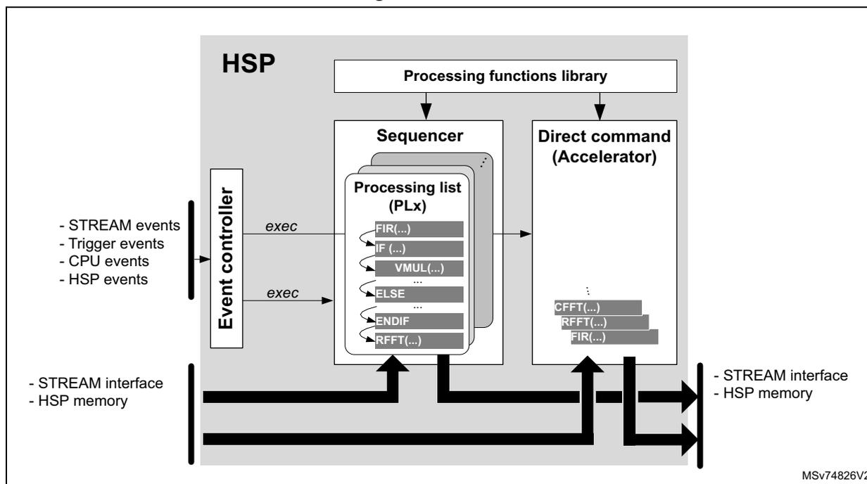
The diagram illustrates the functional view of the HSP. On the left, an 'Event controller' receives inputs: '- STREAM events', '- Trigger events', '- CPU events', and '- HSP events'. It has two 'exec' output lines. The top 'exec' line connects to a 'Sequencer' block, which contains a 'Processing list (PLx)' with instructions: 'FIR(...)', 'IF (...)', 'VMUL(...)', 'ELSE ...', 'ENDIF', and 'RFFT(...)'. The bottom 'exec' line connects to a 'Direct command (Accelerator)' block, which contains instructions: 'CFFT(...)', 'RFFT(...)', and 'FIR(...)'. Above both the 'Sequencer' and 'Direct command' blocks is a 'Processing functions library' block. At the bottom, a thick horizontal bus connects the 'Event controller', 'Sequencer', and 'Direct command' blocks. On the left side of this bus are '- STREAM interface' and '- HSP memory'. On the right side are '- STREAM interface' and '- HSP memory'. The identifier 'MSV74826V2' is in the bottom right corner.
The application can record up to 37 processing lists into the HSP during the runtime. A processing list represents an HSP task. The execution of processing lists is triggered by events. The event sources can be:
- • STREAM interface
- • Trigger signals
- • Software triggers
The HSP offers the following bus interfaces:
- • An AHB slave port interface giving access to the HSP control registers (SP0)
- • An AHB slave port interface giving access to the HSP memories (SP1)
When the data to be processed are 16- or 32-bit integers, the HSP converts them into a 32-bit floating-point format before performing the required processing.
If the data are in 8-bit integer or 32-bit floating-point format, the HSP processes them directly.
Data exchange between the HSP and the application can be done in several ways:
- • Using the BRAM as a shared memory
- • Using data registers via the STREAM interface
After each processing task performed in 32-bit floating-point format, the HSP can provide the data either in floating-point or integer format. Processing performed using an 8-bit integer returns results in 8-bit integer format.
See the user manual HSP processing functions on STM32 MCUs (UM3360) .
Finally, the HSP offers an interrupt interface allowing the application to receive interrupts from a wide variety of events.
19.2 HSP main features
- • AHB slave interface for memories (SP1)
- • AHB slave interface for register control (SP0)
- • Rich set of signal processing commands (such as FFT, FIR, or IIR)
- • Support of 2D convolution for neural networks
- • Operations performed in floating-point single precision compliant with the IEEE-754 standard
The HSP FPU is compliant with the IEEE-754 standard with the following limitations:
- – Denormals are flushed to zero.
- – Only round to the nearest is supported.
- • Supported data formats:
- – Signed/unsigned 16-bit integer format
- – Signed/unsigned 32-bit integer format
- – 32-bit floating-point format
- – 8-bit integer (CNN functions)
- • Trigger inputs
- • Break generation
- • STREAM interface
- • Trigger outputs
- • Interrupt services
Targeted applications:
- • Audio: speech capture
- • Motor control
- • Digital power
- • Metering
19.3 HSP implementation
The table below details the set of features implemented into the product.
Table 143. HSP features (1)
| Feature | Values |
|---|---|
| SRAM instance containing BRAM, CRAM, and DRAM | SRAM4 |
| CRAM size | 20 Kbytes |
| DRAM size | 12 Kbytes |
| BRAM size | 32 Kbytes |
| Global Interrupt (hsp_it) | Yes |
| Error interrupt (hsp_err_it) | - |
| Event interrupt (hsp_evt_it) | - |
| Firmware event interrupt (hsp_fwevt_it) | - |
| HSPDMA and STI function | No |
| Number of DMA channels | - |
| Number of DMA requests, which can be connected to peripherals | - |
| Number of STIAP ports | - |
| Number of STIHP ports | - |
| Number of trigger inputs | 20 |
| Direct ADC interface function | No |
| Number of ADC interfaces | - |
| Maximum number of processing lists | 37 |
1. 'X' = supported, '-' = not supported.
Table 144. HSP memory mapping
| - | CRAM | DRAM | BRAM-A | BRAM-B | BRAM-AB | End of BRAM-AB |
|---|---|---|---|---|---|---|
| Address offset | 0x0000 0000 | 0x0000 5000 | 0x0000 8000 | 0x0000 C000 | 0x0001 0000 | 0x0001 3FFF |
19.4 HSP functional description
19.4.1 HSP block diagram
Figure 68. HSP block diagram
![HSP block diagram showing internal components like MMC, SPE, SPEIF, STREAM, TRGITF, SEG, EVTC, DCMD, MSGB, PARAM, DITC, HITC, TSC, TRGO, TCU, BKITF, CPUIF, and HSP_CTRL. It also shows external connections to AHB, SRAMx (BRAM-B, BRAM-A, DRAM, CRAM), and various pins like hsp_hclk_mem_ck, hsp_hclk_core_ck, hsp_break_in, hsp_trgi[x:0], hsp_break_out[3:0], hsp_bus_ckreq, hsp_it, hsp_err_it, hsp_fwevt_it, hsp_evt_it, hsp_txev, hsp_trgo[3:0], hsp_gpo[7:0], and HSP_SNP[5:0].](/RM0487-STM32U3/f6a7fb17ff6df278c25da65ef8f1cfa5_img.jpg)
The diagram illustrates the internal architecture of the HSP. At the top, the MMC block is connected to an SP1 interface on the left and to SRAMx (containing BRAM-B , BRAM-A , DRAM , and CRAM ) on the right. Below MMC are DROM and CROM . The SPE block (labeled Quad F32, Quad int8 ) is connected to SP0 on the left and to various output pins on the right. Below SPE is the SPEIF block, which contains STREAM , TRGITF , SEG , and EVTC . Below SPEIF is a grid of blocks: DCMD , MSGB , PARAM , DITC , HITC , TSC , TRGO , TCU , and BKITF . Below this grid is the CPUIF block, which is connected to SP0 on the left and to HSP_SNP[5:0] on the right. The entire lower section is enclosed in the HSP_CTRL block. External inputs include hsp_hclk_mem_ck , hsp_hclk_core_ck , hsp_break_in , and hsp_trgi[x:0] (1) . External outputs include hsp_break_out[3:0] , hsp_bus_ckreq , hsp_it , hsp_err_it , hsp_fwevt_it , hsp_evt_it (grouped by (2) ), hsp_txev , hsp_trgo[3:0] , and hsp_gpo[7:0] . The diagram is labeled MSV74828V2.
- 1. The number of trigger inputs depends on the product, see Section 19.3: HSP implementation .
- 2. These interrupt lines are not always connected, see Section 19.3: HSP implementation .
19.4.2 HSP pins and internal signals
Table 145. HSP external pins
| Pin name | Pin type | Comment |
|---|---|---|
| HSP_SNP[5:0] | Output | HSP outputs for debug and diagnostics |
Table 146. HSP internal signals
| Signal name | Signal type | Comment |
|---|---|---|
| hsp_hclk_mem_ck | Input | Bus clock input for memories |
| hsp_hclk_core_ck | Input | Bus clock input for HSP core |
Table 146. HSP internal signals (continued)
| Signal name | Signal type | Comment |
|---|---|---|
| hsp_bus_ckreq | Output | Bus interface clock request output |
| hsp_break_out[3:0] | Output | HSP break output signals |
| hsp_break_in | Input | HSP break input signal |
| hsp_it | Output | HSP global interrupt |
| hsp_err_it (1) | Output | HSP error interrupt |
| hsp_evt_it (1) | Output | HSP event interrupt |
| hsp_fwevt_it (1) | Output | HSP firmware event interrupt |
| hsp_txev | Output | HSP direct command complete event. |
| hsp_trgi[x:0] (2) | Input | HSP trigger input signals |
| hsp_trgo[3:0] | Output | HSP trigger output signals |
| hsp_gpo[7:0] | Output | HSP general-purpose output signals |
| hsp_dbgmcu_stp | Input | Halt request from DBGMCU (check DBG section to see if the feature is available) |
- 1. This interrupt line is not always connected to the interrupt controller, see Section 19.3: HSP implementation .
- 2. The number of trigger input signals depends on the product, see Section 19.3: HSP implementation .
The table below shows how HSP trigger inputs are connected in the product.
Table 147. HSP trigger input connections
| Input trigger name | Trigger source |
|---|---|
| hsp_trgi1 | gpdma1_chan_tc[0] |
| hsp_trgi1 | gpdma1_chan_tc[1] |
| hsp_trgi2 | gpdma1_chan_tc[2] |
| hsp_trgi3 | gpdma1_chan_tc[3] |
| hsp_trgi4 | EXTI0 |
| hsp_trgi5 | EXTI1 |
| hsp_trgi6 | TIM1 TRGO |
| hsp_trgi7 | TIM1 TRGO2 |
| hsp_trgi8 | TIM2 TRGO |
| hsp_trgi9 | TIM3 TRGO |
| hsp_trgi10 | TIM6_TRGO |
| hsp_trgi11 | TIM7_TRGO |
| hsp_trgi12 | TIM8_TRGO |
| hsp_trgi13 | TIM8_TRGO2 |
| hsp_trgi14 | TIM15_TRGO |
| Input trigger name | Trigger source |
|---|---|
| hsp_trgi15 | LPTIM1_CH1 |
| hsp_trgi16 | LPTIM1_CH2 |
| hsp_trgi17 | LPTIM2_CH1 |
| hsp_trgi18 | LPTIM2_CH2 |
| hsp_trgi19 | ADF_SAD_DET |
The table below shows how HSP trigger outputs are connected in the product.
Table 148. HSP trigger output connections for STM32U3B5/3C5| Output trigger name | Trigger destination |
|---|---|
| hsp_trgo0 | GPDMA1 dma_trig[34] |
| hsp_trgo1 | GPDMA1 dma_trig[35] |
| hsp_trgo2 | GPDMA1 dma_trig[36] |
| hsp_trgo3 | GPDMA1 dma_trig[37] |
| hsp_gpo0 | GPDMA1 dma_trig[38] |
| hsp_gpo1 | GPDMA1 dma_trig[39] |
| hsp_gpo2 | GPDMA1 dma_trig[40] |
| hsp_gpo3 | GPDMA1 dma_trig[41] |
| hsp_gpo[7:4] | - |
The table below shows how HSP break outputs are connected in the product.
Table 149. HSP break connections| Signal name | Trigger source |
|---|---|
| hsp_break_out0 | TIM1_brk1[3] TIM1_brk2[3] TIM8_brk1[3] TIM8_brk2[3] |
| hsp_break_out1 | TIM1_brk1[4] TIM1_brk2[4] TIM8_brk1[4] TIM8_brk2[4] |
| hsp_break_out2 | TIM15_brk1[3] TIM16_brk1[3] TIM17_brk1[3] |
Table 149. HSP break connections (continued)
| Signal name | Trigger source |
|---|---|
| hsp_break_out3 | TIM15_brk1[4] TIM16_brk1[4] TIM17_brk1[4] |
| hsp_break_in | - |
19.4.3 Floating-point format
The HSP is a powerful and flexible signal processing engine, able to perform operations on data located into its shared memory (BRAM).
The HSP can work by processing data blocks (vector) or sample per sample. The latter mode is particularly helpful for closed-loop control.
The HSP supports several kinds of data input formats: 8-, 16-, 32-bit integers, and 32-bit floating points. For simplification, this document refers to 32-bit floating points as “float32”. In the same way, signed 8-bit integers are named “int8”.
The SPE embedded into the HSP performs its computation in single-precision floating points (float32) or 8-bit integers (int8).
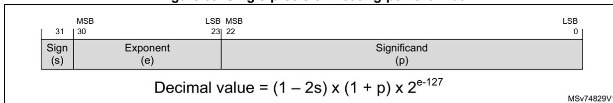
As defined by the IEEE-754 standard, the single-precision floating-point numbers are stored into the memory as shown in the figure below.
Figure 69. Single-precision floating-point format
| MSB | LSB | MSB | LSB | ||||
| 31 | 30 | 23 | 22 | 0 | |||
| Sign (s) | Exponent (e) | Significand (p) | |||||
Decimal value = \( (1 - 2s) \times (1 + p) \times 2^{e-127} \)
MSV74829V1
The single precision floating-point number includes:
- • A sign bit
- • A significand part of 23 bits
- • An exponent of 8 bits (-126 to + 127)
The first leading 1 bit of a normalized significand is “hidden”, or “implicit”, extending the significand to 24-bit precision.
Floating point greatly simplifies working with large numbers, up to about \( \pm 3.4e^{38} \) , and small numbers down to about \( \pm 1.17e^{-38} \) .
The HSP embeds the capability of converting integers into float32 and vice versa.
The HSP also supports integer 8-bit operations. They are dedicated to run convolutional neural networks. In this mode, the internal accumulator size is 32 bits to keep the best accuracy.
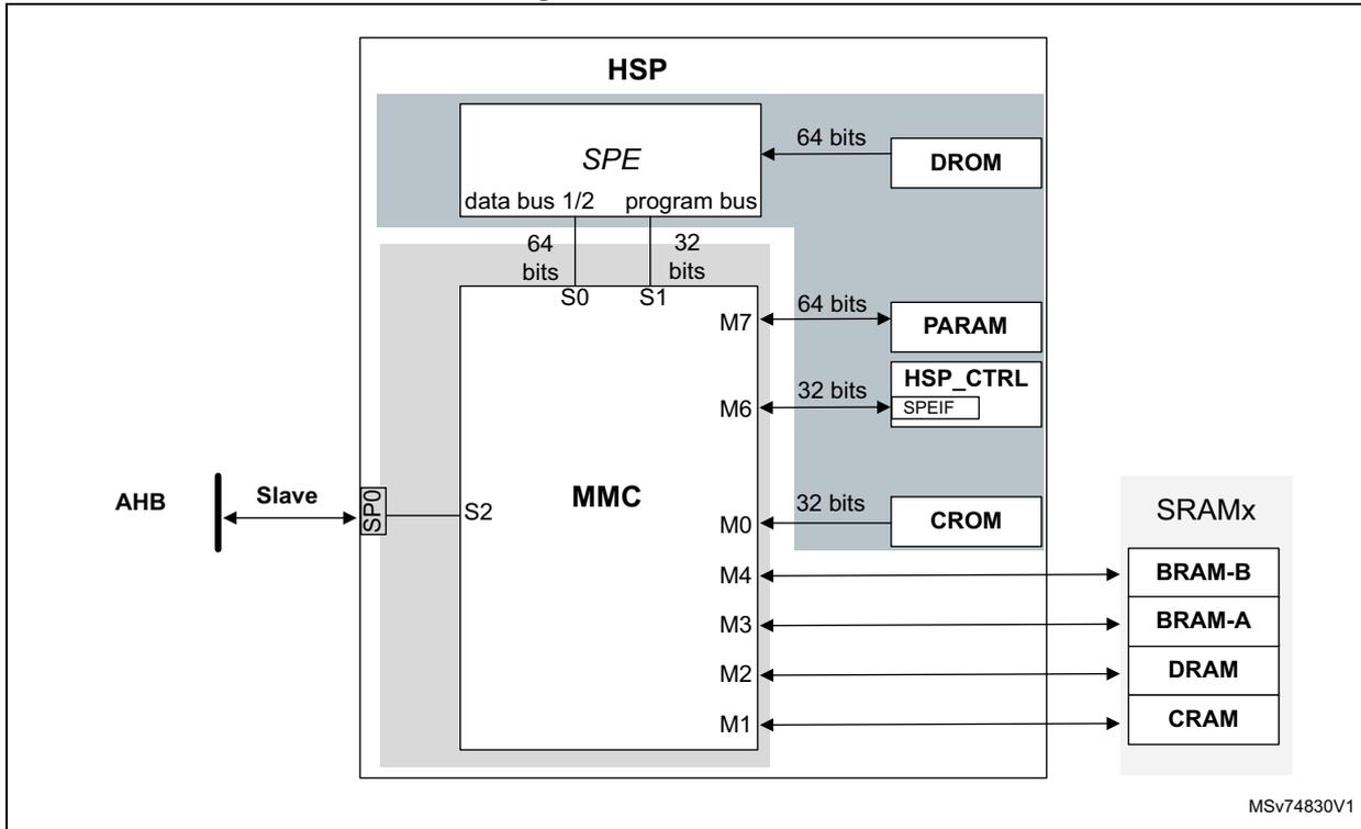
19.4.4 Memory management
A memory controller (MMC) manages the SRAM shared with the HSP. This SRAM can be used by the application like any other SRAM or dedicated to HSP activity when the HSP is activated (see Section 19.3: HSP implementation to check which SRAM is shared with the HSP on the product). This SRAM is split into five different sections when the application intends to use the HSP. The different sections are listed below:
- • The code RAM (CRAM) section, containing the HSP firmware program, plug-ins, and processing lists
- • The data RAM (DRAM) section, containing SPE sensitive data and processing list parameters
- • The buffer RAM A (BRAM-A), RAM B (BRAM-B), and RAM-AB sections, containing the working data, filter coefficients, and filter states
In addition, the HSP embeds a code ROM and a data ROM:
- • The code ROM (CROM) contains the generic signal processing functions library.
- • The data ROM (DROM) contains constants, such as FFT coefficients.
Figure 70. MMC overview
Memory protection and sharing
The access to the memory shared with the HSP is controlled by the MMC (memory controller) block. After a system reset, this SRAM is available for the application, and can be used as a general-purpose SRAM.
Note: This SRAM can be enabled or disabled via an RCC control bit. Make sure it is enabled before using it.
The BRAM-A, BRAM-B, and BRAM-AB sections are always shared with the application and are generally used for data exchanges and working buffers.
The application can restrict the access to CRAM and DRAM sections with the CDRLCK[1:0] bitfield in the HSP control register (HSP_CR) . CRAM and DRAM access filtering works as follows:
- • CDRLCK[1:0] = 0: read and write access through the AHB slave of CRAM and DRAM is allowed.
- • CDRLCK[1:0] = 1: write access to CRAM and DRAM is not allowed. Any read access is allowed. Only an HSP reset can restore write access to these memories.
- • CDRLCK[1:0] = 2 or 3: read and write access to CRAM and DRAM is not allowed. Only an HSP reset can restore read and write access to these memories.
An invalid application read access to a RAM protected by CDRLCK[1:0] returns 0. An invalid application write access to a RAM protected by CDRLCK[1:0] is ignored. In both cases, the ACCERRF and SAHBERR flags are set.
Accessing above BRAMAB_END (see Figure 71 ) also generates a bus error. The ACCERRF and SAHBERR flags are set as well.
See Section 19.4.12: HSP interrupt controller (HITC) .
The access restrictions programmed with CDRLCK[1:0] do not affect the SPE.
Note:
The application must first enable the hsp_hclk_core_ck (via the RCC) to change the value of CDRLCK[1:0]. Once CDRLCK[1:0] is updated, the hsp_hclk_core_ck can be disabled.
If the HSP was previously activated, it is recommended to reset the HSP before reusing the shared SRAM. The HSP reset is handled by the RCC.
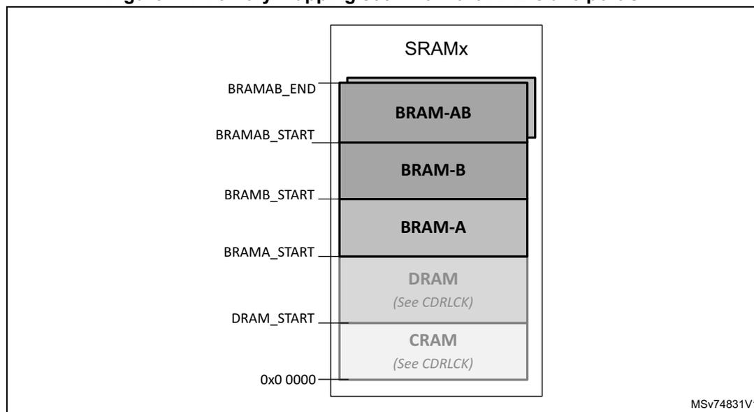
Table 150 shows the address offset of each memory section. The BRAM is seen as two single ports, or like a dual port (BRAM-AB). Depending on the operations requested from the HSP, the application must use a dual-port BRAM or single-port BRAMs.
Table 150. Memory mapping seen from MMC AHB slave (1)
| Section start/stop acronym | Generic address offset (bytes) |
|---|---|
| BRAMAB_END | BRAMAB_START + (BRAM_SIZE * 512) - 1 |
| BRAMAB_START | BRAMB_START + BRAM_SIZE * 512 |
| BRAMB_START | BRAMA_START + BRAM_SIZE * 512 |
| BRAMA_START | DRAM_START+ DRAM_SIZE * 1024 |
| DRAM_START | CRAM_SIZE * 1024 |
| CRAM_START | 0 |
- 1. CRAM_SIZE, DRAM_SIZE, and BRAM_SIZE represent the size, in Kbytes, of CRAM, DRAM, and BRAM respectively. Refer to section Section 19.3: HSP implementation for memory size.
As shown in Figure 71 , the application sees the SRAM shared with the HSP as a contiguous memory block, with the capacity to restrict access to CRAM and DRAM blocks. When the HSP is enabled, the CPU can still access this SRAM, but the HSP also uses it.
For the HSP to run safely, it is recommended to write-protect CRAM and DRAM as soon as the application has loaded the main firmware code and its data into CRAM and DRAM.
The CPU can access:
- • BRAM-A, BRAM-B, and DRAM in 8, 16, or 32 bits (and in 64 bits, if the product supports it)
- • CRAM in 8, 16, or 32 bits.
Figure 71. Memory mapping seen from the AHB slave port SP1
Memory resource arbitration
When the HSP is running, the BRAM-AB, BRAM-A, or BRAM-B can be accessed by the SPE or by the application through the AHB slave interface.
To keep the best SPE performances, the MMC arbiter gives the highest priority to the SPE. However, some processing done by the SPE can take 100% of the BRAM resource, preventing the other requesters from accessing the BRAM. To avoid this, the MMC ensures that if the application requests the BRAM resource, the resource is granted in the worst case after 16, 8, or 4 cycles. BARB[1:0] in the HSP control register (HSP_CR) allows the selection of one of these values.
As shown in Figure 72 , a fixed-priority arbiter (FPA) ensures that the request coming from the AHB slave interface is granted at most every 16, 8, or 4 cycles. This mechanism prevents important degradation of SPE performances.
The right part of the figure shows an arbitration example.
- • The SPE occupies 100% of the BRAM bandwidth. After k clock periods, the AHB slave must access the BRAM-AB.
- • After N cycles (k + N), the AHB slave can perform its transaction. N can be either 4, 8, or 16.
When the SPE no longer uses the BRAM, the AHB slave transactions are served immediately using the full bandwidth.
Figure 72. BRAM arbitration
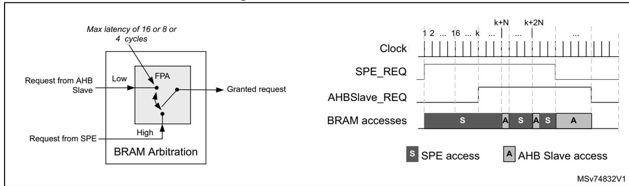
The diagram illustrates the BRAM arbitration mechanism. On the left, a block diagram shows the BRAM Arbitration unit with two inputs: 'Request from AHB Slave' (Low) and 'Request from SPE' (High). The unit contains an FPA (Fixed Priority Arbiter) and outputs a 'Granted request'. A note indicates a 'Max latency of 16 or 8 or 4 cycles'. On the right, a timing diagram shows the 'Clock', 'SPE_REQ', 'AHBSlave_REQ', and 'BRAM accesses' signals over time. The 'BRAM accesses' signal is divided into segments labeled 'S' (SPE access) and 'A' (AHB Slave access). The legend indicates 'S SPE access' and 'A AHB Slave access'. The reference 'MSv74832V1' is shown in the bottom right corner.
19.4.5 HSP boot
Before running the HSP, the application must copy the HSP firmware code into the code RAM (CRAM) and data RAM (DRAM). Additionally, some applications can also request to copy plug-ins. Plug-ins are extra binary codes provided by STMicroelectronics and used to correct the limitations of existing processing functions, or to add new processing functions not included in the original product.
The binary files must be copied as shown in Figure 73 :
- • If no plug-ins are loaded, the application must write a termination word (0xFFFF FFFF) right after the copied binary code.
- • If plug-ins must be added, they must be copied contiguous to the HSP firmware binary code, and the termination word must be added right after the last plug-in.
Figure 73. HSP code loading
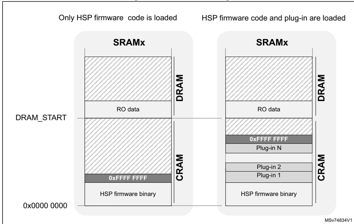
The diagram illustrates two memory layout scenarios for HSP code loading within an SRAMx block, which is divided into DRAM and CRAM sections.
- Left Scenario: Only HSP firmware code is loaded
- The SRAMx block contains a DRAM section at the top with 'RO data'.
- Below the DRAM section is the CRAM section.
- The CRAM section contains a block labeled '0xFFFF FFFF' followed by 'HSP firmware binary' at the bottom.
- The address '0x0000 0000' is indicated at the bottom left of the CRAM section.
- A horizontal dashed line labeled 'DRAM_START' points to the boundary between the DRAM and CRAM sections.
- Right Scenario: HSP firmware code and plug-in are loaded
- The SRAMx block contains a DRAM section at the top with 'RO data'.
- Below the DRAM section is the CRAM section.
- The CRAM section contains several blocks: '0xFFFF FFFF', 'Plug-in N', 'Plug-in 2', 'Plug-in 1', and 'HSP firmware binary' at the bottom.
MSV74834V1
Refer to Section 19.3: HSP implementation to find which SRAM instance contains BRAM, CRAM, and DRAM on the product, as well as the relative address offset.
The application must execute the sequence below to run the HSP properly:
- 1. Reset the HSP using the reset bit in the RCC.
- 2. Copy the HSP firmware binary code and the RO data into the CRAM and DRAM sections respectively. Copy plug-in binaries, if any, into the CRAM.
- 3. Enable the HSP core clock via the RCC.
- 4. If needed, protect CRAM and DRAM sections against accidental corruption via CDRLCK[1:0].
- 5. Set the BOOTEN bit to run the HSP. The HSP executes the code starting at the CRAM base address of the CRAM, and enters the HSPCFG state.
- 6. In HSPCFG state, the HSP firmware performs the following operations:
- a) Initialize the internal HSP subblocks. TSKLUT is also initialized to only allow the activation of the supervisor (PLSUP) or Direct Command Accelerator functions (PLDCMD).
- b) Copy the firmware versions and SPE into HSP_FWVERR and HSP_SPEVERR.
- c) Set BSTAT[3:0] to 1, indicating it is waiting for the FW_INIT command.
- 7. The HSP firmware is now ready to accept the FW_INIT command.
- 8. When the FW_INIT command is complete, the HSP firmware activates the plugin codes, if any. This phase sets BSTAT[3:0] to 8.
- 9. The HSP enters the RUN phase and the WFE state, and sets BSTAT[3:0] to 2. As soon as an enabled event is activated, the HSP exits the WFE state and goes to:
- a) PLRUN if the selected event is valid (meaning it is associated with an existing processing list). The HSP firmware executes the processing list corresponding to the selected event, and goes back to WFE.
- b) PLSUP if the selected event corresponds to the supervisor. The HSP firmware executes the command sent by the application and goes back to WFE. Processing lists are created in this mode.
- c) PLDCMD if a direct command is programmed via the DCMD block.
- d) PLFAIL if the selected event is not valid.
- 6. In HSPCFG state, the HSP firmware performs the following operations:
- In PLDCMD mode, the HSP firmware executes the command sent by the application and goes back to WFE.
- In PLFAIL, the HSP firmware sets the FWERRF bit, sets the firmware error code in FWERRN[9:0], and goes back to WFE.
If an error occurs during this initialization process, the HSP firmware goes to the CFGFAIL state. In the CFGFAIL state, BSTAT[3:0] is set to 9. To set the HSP firmware back to the HSPCFG state, the HSP must be reset through the RCC.
When the HSP firmware initialization is completed, the application can enable the events, which are supposed to trigger the programmed processing list.
BOOTEN, CDRLOCK[1:0], and BSTAT[3:0] are located in the HSP control register (HSP_CR) .
Figure 74. HSP start-up
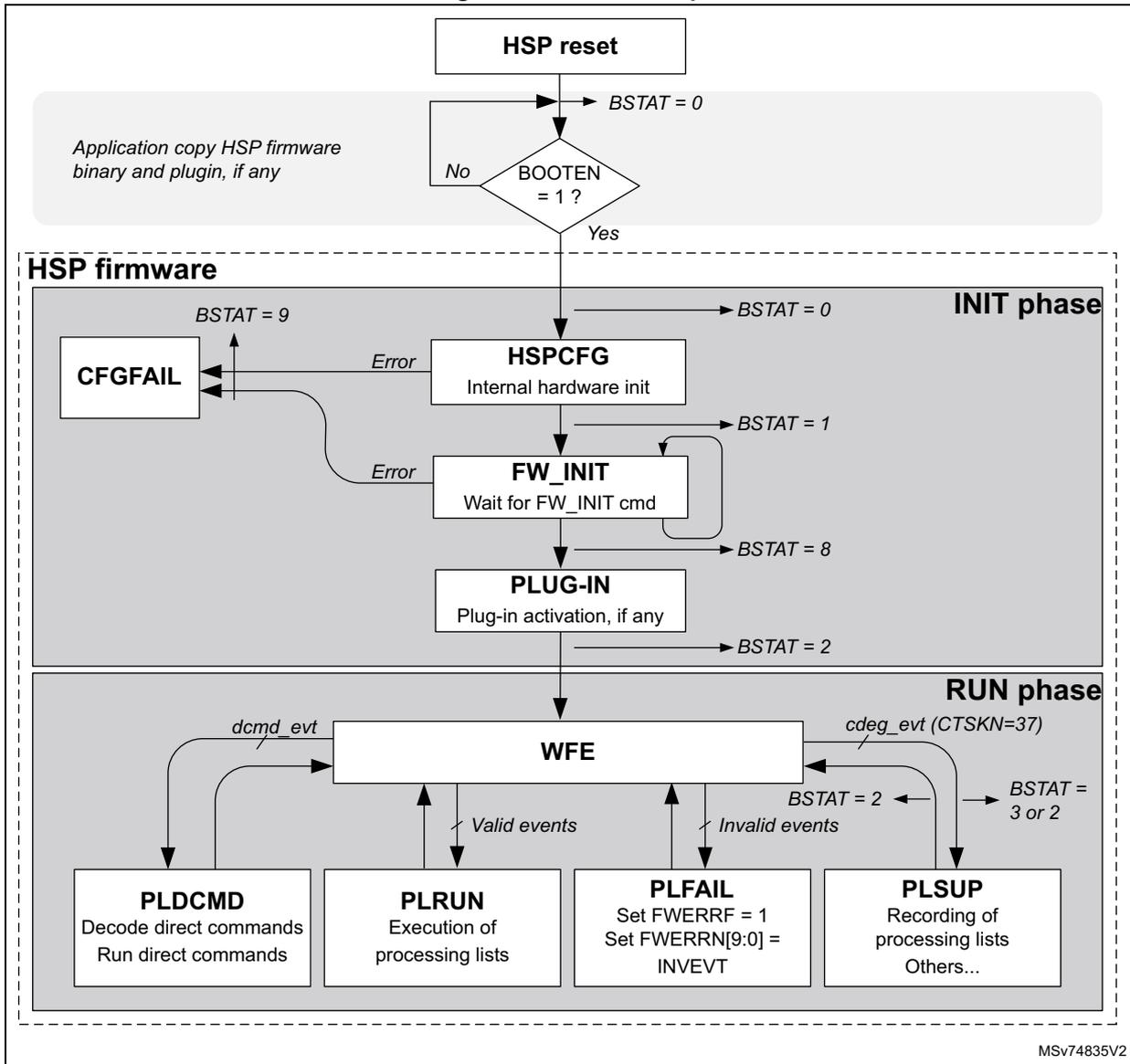
The flowchart illustrates the HSP start-up process. It begins with an HSP reset , which sets BSTAT = 0 . A note indicates that the application should copy HSP firmware binary and plugin, if any. A decision diamond asks if BOOTEN = 1 ? . If No , the process loops back to the start. If Yes , it enters the HSP firmware section, which is divided into INIT phase and RUN phase .
In the INIT phase :
- HSPCFG (Internal hardware init) is executed, setting BSTAT = 0 .
- FW_INIT (Wait for FW_INIT cmd) is executed, setting BSTAT = 1 . An Error from CFGFAIL (which sets BSTAT = 9 ) can occur here.
- PLUG-IN (Plug-in activation, if any) is executed, setting BSTAT = 8 .
- After PLUG-IN , BSTAT = 2 is set.
In the RUN phase , the WFE (Wait For Event) loop is entered. It handles dcmd_evt and cdeg_evt (CTSKN=37) . The loop can lead to PLDCMD (Decode direct commands, Run direct commands), PLRUN (Execution of processing lists), PLFAIL (Set FWERRF = 1, Set FWERRN[9:0] = INVEVT), or PLSUP (Recording of processing lists, Others...). Valid events lead to PLRUN , while Invalid events lead to PLFAIL . PLFAIL and PLSUP both set BSTAT = 2 , which then transitions to BSTAT = 3 or 2 .
MSV74835V2
The table below shows the different values BSTAT can take.
Table 151. BSTAT possible values
| Conditions | BSTAT[3:0] |
|---|---|
| Information | |
| Default value after reset | 0b0000 |
| The HSP firmware started | 0b0010 |
| The HSP firmware waits for firmware initialization command (FW_INIT) | 0b0001 |
| The HSP firmware is in RUN phase | 0b0011 |
| The HSP firmware is recording a processing list | 0b0100 |
| Errors | |
| The HSP firmware is in CFGFAIL state | 0b1100 |
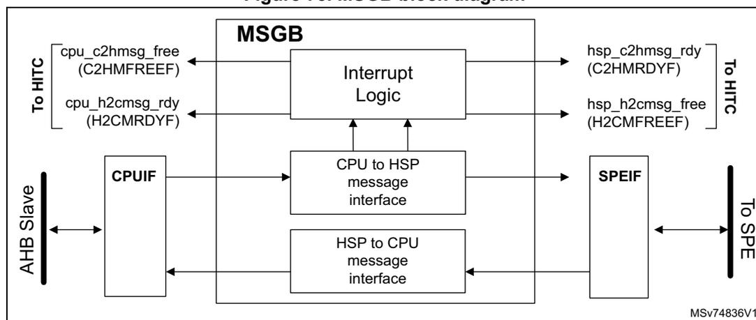
19.4.6 Message box (MSGB)
The message box (MSGB) offers various services dedicated to the HSP firmware configuration.
The MSGB block contains an HSP-to-CPU and a CPU-to-HSP message interface with:
- • Synchronization flags and interrupt capabilities
- • Two payload registers
The MSGB is generally used with the HSP parameter register x (HSP_PARAMRx) to provide the message payload. Messages are used to configure the HSP firmware part, especially to record the processing list.
Figure 75. MSGB block diagram
CPU to HSP message interface
Using polling mode
When the CPU wants to send a message to the HSP, it has to do the following:
- 1. Read C2HSEM in the HSP CPU-to-HSP semaphore register (HSP_C2HSEMR) .
- 2. Wait until C2HSEM = 0, indicating that the previous message has been read by the HSP and a new message can be transferred.
- 3. Write a new value in the HSP CPU-to-HSP message data register (HSP_C2HMSGDR) .
- 4. Set C2HSEM.
On its side, the HSP does the following:
- 1. Read the C2HSEM bit.
- 2. Wait until C2HSEM = 1, indicating that a new message is available.
- 3. Read the C2HDATA.
- 4. Clear C2HSEM to indicate that the message has been read.
Using interrupt mode
The MSGB can generate interrupts to the CPU when the CPU-to-HSP mailbox is ready to receive a new message (through the C2HMFREEF flag).
The CPU must first enable the interrupts by executing the sequence below:
- 1. Clear the C2HMFREEF flag by setting C2HMFREEC in the HSP events interrupt clear register (HSP_EVT_ICR) .
- 2. Allow the C2HMFREEF flag to generate an interrupt by setting C2HMFREEIE in the HSP events interrupt enable register (HSP_EVT_IER) .
When an event interrupt occurs, the interrupt subroutine (ISR) must do the following:
- 1. Read the C2HMFREEF flag in the HSP events interrupt status register (HSP_EVT_ISR) .
- 2. If C2HMFREEF is set:
- – The CPU can clear this flag by setting C2HMFREEC.
- – The CPU can write a new message.
- – When the CPU wants to notify the HSP that a new message is available, C2HSEM must be set.
The last two steps can be done outside the ISR.
HSP-to-CPU message interface
Using polling mode
When the HSP wants to send a message to the CPU, it does the following:
- 1. Read the H2CSEM flag.
- 2. Wait until H2CSEM = 0, indicating that the previous message has been read by the CPU and the content of HSP_SPE_H2CMSGDR can be overwritten.
- 3. Write the new value into C2HDATA.
- 4. Set H2CSEM.
On its side, the CPU does the following:
- 1. Read H2CSEM in the HSP HSP-to-CPU semaphore register (HSP_H2CSEMR) .
- 2. Wait until H2CSEM = 1, indicating that a new message is available.
- 3. Read the HSP HSP-to-CPU message data register (HSP_H2CMMSGDR) .
- 4. Clear H2CSEM in the HSP HSP-to-CPU semaphore register (HSP_H2CSEMR) to indicate that the message has been read.
Note: Handling the MSGB in polling mode also sets H2CMRDYF and C2HMFREEF. Prior to using these flags, the software must clear them.
If the CPU and the HSP set and clear C2HSEM at the same time respectively, C2HSEM is cleared.
If the CPU and the HSP set and clear C2HSEM at the same time respectively, C2HSEM is cleared.
Using interrupt mode
The MSGB can generate interrupts to the CPU when a new message is available for the CPU (through the H2CMRDYF flag).
The CPU must first enable the interrupts by executing the sequence below:
- 1. Clear the H2CMRDYF flag by setting the H2CMRDYC bit in the HSP events interrupt clear register (HSP_EVT_ICR) .
- 2. Allow the H2CMRDYF flag to generate an interrupt by setting the H2CMRDYIE bit in the HSP events interrupt enable register (HSP_EVT_IER) .
When an event interrupt occurs, the interrupt subroutine (ISR) must do the following:
- 1. Read the H2CMRDYF flag in the HSP events interrupt status register (HSP_EVT_ISR) .
- 2. If H2CMRDYF is set:
- – The CPU can clear this flag by setting H2CMRDYC.
- – The CPU can read the message.
- – When the CPU decides to free the message box, the H2CSEM bit must be cleared.
The last two steps can be done outside the ISR.
19.4.7 Direct command interface (DCMD)
The direct command interface (DCMD) is dedicated to the execution of direct commands, reducing the command overhead in an efficient way. It is used for HSP accelerator mode. This block is controlled by the HSP with a PLDCMD dedicated processing list (refer to Section 19.6.4: Executing direct commands (accelerator mode) ).
The DCMCD provides the following services:
- • Direct command ID register, for triggering events
- • Up to three data pointer interfaces
- • Status flags
The DCMD is generally used with the HSP parameter register x (HSP_PARAMRx) to provide the parameters corresponding to the command that the application wants to execute.
Figure 76. DCMD block diagram
Prior to running a direct command, the SPE must perform the following preliminary operations:
- 1. Decode the command
- 2. Adapt the data pointer values
- 3. Execute the command
To reduce latency in command decoding, the DCMD block allows the SPE to start command decoding while the CPU is still providing the parameters.
By default, the DCMD block is enabled. DCMDDIS in the HSP BUFF configuration register (HSP_BUFFCFGR) controls the enabling and disabling of this function. This bit is write-once after an HSP reset. If the application wants to ensure that the DCMD cannot be accidentally disabled, it must clear DCMDDIS. If the application wants to disable the DCMD, DCMDDIS must be set.
The CPU can transmit the command ID to be executed by writing the command ID in the HSP DCMD command ID register (HSP_DCMDIDR) .
A write access to this register triggers two actions:
- • It sets the DCBSY flag.
- • It asserts the DCMD event ( dcmd_evt ).
dcmd_evt triggers a processing list dedicated to the execution of direct commands. The number of this processing list is 38, and its priority is set to 26.
The DCBSY flag is cleared by the SPE when the direct command execution is completed.
The HSP DCMD address pointer register x (HSP_DCMDPTRx) allows the CPU to provide to the SPE the address pointers requested by the direct commands.
When the CPU writes an address pointer into one of the HSP_DCMDPTRx registers, the HSP hardware sets the corresponding PTRF[x] flag in the HSP DCMD pointer status register (HSP_DCMDPTRSR) .
When the SPE reads this pointer, the DCMD hardware sets the corresponding PTRFx bit to zero. The DCMD also provides a bit (RDOG) indicating if the SPE is performing a read operation of one of the three data pointers. This bit can be used in a debug phase to check if the SPE is waiting for a data pointer value.
Note: If the SPE reads a pointer register not yet updated by the CPU, the SPE remains frozen on the read operation until the CPU has updated the corresponding pointer register.
The DCMD also offers the possibility to generate an interrupt when the DCBSY flag is cleared, meaning that the command has been completed. The interrupt is enabled by setting DCDONEIE in the HSP events interrupt enable register (HSP_EVT_IER) .
Figure 77 shows a typical example of a command programming sequence, and the behavior of the various signals. During an initialization sequence, the CPU is assumed to clear DCMDDIS.
- 1. The CPU writes the command ID in the HSP DCMD command ID register (HSP_DCMDIDR) . The DCBSY and dcmd_evt are set (#1 in the figure).
- 2. The CPU writes data parameters in the HSP parameter register x (HSP_PARAMRx) (#2 in the figure).
- 3. The CPU starts to write the first two address pointers in the HSP DCMD address pointer register x (HSP_DCMDPTRx) . As soon as the EVTC allows it, task number 26 is activated (#3 in the figure).
- 4. The SPE first reads the command ID to check which command must be executed, and then starts to read the necessary address pointers. The first two address pointers are already available, but the SPE remains blocked for several cycles when reading the third pointer, because the CPU did not yet write it (#4 in the figure).
- 5. When the CPU writes the third pointer, the SPE gets it translated, and the command can be executed (#5 in the figure).
- 6. When the command execution is completed, the SPE clears the DCBSY flag. This action clears the dcmd_evt (#6 in the figure).
- 7. Finally, if DCDONEIE is set, an interrupt can be generated to inform that task execution has been completed. Then the CPU can clear the interrupt (and DCDONEF flag) by setting the clear bit (DCDONEC).
Figure 77. Direct command programming example
![Timing diagram for direct command programming example showing CPU operations, SPE operations, and various signal states (DCBSY, DCDONEF, PTRF[0-2], RDOG, dcmd_evt) over time. The diagram is divided into two main horizontal tracks: CPU operations and SPE operations. CPU operations include writing parameters, command ID, and pointers into HSP registers. SPE operations include reading command ID, pointers, and executing the command. Signal lines show the state of DCBSY, DCDONEF, PTRF[0], PTRF[1], PTRF[2], RDOG, and dcmd_evt. A task number 'Task 38' is shown. The diagram is labeled with numbered steps 1-6 and includes a reference code MSV74838V1.](/RM0487-STM32U3/7fb0a0df445fd4a349594ca52057c1d9_img.jpg)
The diagram illustrates the timing for direct command programming. It shows the sequence of events between the CPU and the SPE.
1. CPU writes parameters into HSP_PARAMRx and command ID into HSP_DCMDDDR.
2. CPU writes pointer into HSP_DCMDPTR0.
3. CPU writes pointer into HSP_DCMDPTR1.
4. SPE reads command ID, read pointer 0, and read pointer 1.
5. CPU writes pointer into HSP_DCMDPTR2.
6. SPE reads pointer 2, executes the command, and clears DCMDF.
Signals shown include DCBSY (active low), DCDONEF (active low), PTRF[0], PTRF[1], PTRF[2] (active high), RDOG (active low), and dcmd_evt (active high). The task number is set to Task 38. The CPU sets DCDONEC to 1 after the command is executed.
If the SPE reads a data pointer not written by the CPU, the SPE remains blocked in the reading operation. The SPE can no longer serve interrupts, nor enter debug mode. The SPE can exit this freeze state through one of the following actions:
- • The application provides the expected data pointer.
- • DCMDDIS is set (if possible). The SPE unfreezes, but executes a command with an invalid pointer, which could be unsafe.
- • The HSP is reset.
The HSP also provides a signal event for the CPU named hsp_txev , indicating that the current direct command execution has been completed. Every time a direct command execution is completed, a single-cycle pulse is generated. DCMDEVEN in the HSP control register (HSP_CR) allows this function activation (see also Section 19.4.12: HSP interrupt controller (HITC) ).
19.4.8 STREAM interface
The STREAM interface can be used if the application wants to trigger an HSP processing list when data are sent to or read from the STREAM interface. It allows the application to set up source- or sink-driven processing.
For example, a DAC associated with a DMA device can take its data from the STREAM interface. As soon as the STREAM interface is read by the DMA device, the SPE is advised and the associated processing list, recorded by the application during an initialization phase, is executed immediately. Typically, this processing list prepares the next sample for the DAC.
Conversely, an ADC associated with a DMA device can provide its data to the STREAM interface. As soon as the STREAM interface is written by the DMA device, the SPE is advised and the associated processing list, recorded by the application during an initialization phase, is executed immediately. Typically, this processing list processes the incoming sample and frees the STREAM interface for the next data.
Figure 78. STREAM block diagram
![Figure 78. STREAM block diagram. The diagram shows the internal architecture of the STREAM interface. On the left, a 'To SoC' connection leads to a 'REGIF' block. The 'REGIF' block connects to four 32-bit buffers: 'BUFF[0]', 'BUFF[1]', 'BUFF[2]', and 'BUFF[3]'. Each buffer has 'C2H' (CPU-to-HSP) and 'H2C' (HSP-to-CPU) input paths. Each buffer also outputs 'buff_err[x]' and 'buff_rxe_txne[x]' signals. All four buffers connect to a central 'BUF CMB' (Buffer Combiner) block. The 'BUF CMB' block outputs 'buff_att[x]' and 'buff_evt[x]' signals to a 'PRC' (Processor) block. Above the 'PRC' block is an 'SPEIF' (SPE Interface) block containing an 'I2F' (Interconnect to SPE) component, which connects 'To SPE'.](/RM0487-STM32U3/390ff4252a12484793ac68e3fe31e302_img.jpg)
The STREAM interface provides up to four data buffers of 32 bits. Each of them can be configured either in the CPU-to-HSP direction (C2H) or the HSP-to-CPU direction (H2C). Buffers configured in CPU-to-HSP direction are called C2HBUFF in this document, and buffers configured in HSP-to-CPU direction are called H2CBUFF.
These buffers can be accessed by the application through the HSP BUFFx data register x (HSP_BUFFxDR) .
The data provided by the CPU (C2H direction) can be converted to float32 automatically if the I2FEN bit in the HSP BUFF configuration register (HSP_BUFFCFGR) is set.
The conversion from integer to float32 only works for the following input formats:
- • Signed integers up to 32 bits. The sign extension must always be performed up to 32 bits. The accuracy of a signed 32-bit integer is reduced to 24 bits due to the float32 format.
- • Unsigned integers up to 31 bits. Bit 31 must be cleared. The accuracy is limited to 24 bits due to the float32 format.
The STREAM buffers configured in the C2H direction assert the buff_att signal when a data is written into a STREAM buffer by the application. The buff_att signal remains active as long as the SPE does not read the corresponding STREAM buffer.
The STREAM buffers configured in the H2C direction assert the buff_att signal when they are empty. The buff_att event signal remains active as long as the SPE does not write data into the corresponding STREAM buffer.
The BUFcmb block adds additional flexibility by combining the buff_att[x] signals to generate the buffer events ( buff_evt[x] ). The BUFcmb allows the generation of the buff_evt[x] event, when the corresponding buff_att[x] signal is activated or when both buff_att[x] and buff_att[x+1] signals are activated. The BUFcmb is configured in the HSP BUFF configuration register (HSP_BUFFCFGR) .
Figure 79. BUFcmb details
![Diagram of BUFcmb details showing four input signals (buff_att[0] to buff_att[3]) entering a chain of logic blocks labeled COMB0, COMB1, and COMB2. Each block contains an AND gate and an OR gate with a multiplexer. The outputs are buff_evt[0] to buff_evt[3]. A small text 'MSV74843V1' is in the bottom right corner.](/RM0487-STM32U3/bd49af920c6819521415b36d5e14491e_img.jpg)
The table below lists some of the possible configurations:
Table 152. BUFFcmb programming examples
| COMB2 | COMB1 | COMB0 | Outputs | |
|---|---|---|---|---|
| 0 | 0 | 0 | → | buff_evt[x] generated when buff_att[x] is activated |
| 1 | 0 | 1 | → | buff_evt[0]
generated when
buff_att[0]
&
buff_att[1]
are activated buff_evt[1] generated when buff_att[1] is activated buff_evt[2] generated when buff_att[2] & buff_att[3] are activated buff_evt[3] generated when buff_att[3] is activated |
Table 152. BUFFCMB programming examples (continued)
| COMB2 | COMB1 | COMB0 | Outputs | |
|---|---|---|---|---|
| 0 | 1 | 1 | → | buff_evt[0]
generated when
buff_att[0]
&
buff_att[1]
&
buff_att[2]
are activated buff_evt[1] generated when buff_att[1] & buff_att[2] are activated buff_evt[2] generated when buff_att[2] is activated buff_evt[3] generated when buff_att[3] is activated |
| 1 | 1 | 1 | → | buff_evt[0]
generated when
buff_att[0]
&
buff_att[1]
&...&
buff_att[3]
are activated buff_evt[1] generated when buff_att[1] & buff_att[2] & buff_att[3] are activated buff_evt[2] generated when buff_att[2] & buff_att[3] are activated buff_evt[3] generated when buff_att[3] is activated |
The CPU can configure the buffer directions and the BUF CMB with the HSP BUFF configuration register (HSP_BUFFCFGR) .
The STREAM interface is activated by setting STREAMEN in the HSP BUFF configuration register (HSP_BUFFCFGR) . When STREAMEN is set, it is no longer possible to change the buffer direction, nor to modify the BUFFCMB configuration.
Note: Clearing STREAMEN resets the STREAM block, and all pending buffer events are cleared. Any write access operation to the STREAM buffers is ignored, and read access returns the last data.
The STREAM interface generates an error signal for each buffer and the error signals buff_err[3:0] are asserted:
- • If new data are written into a buffer configured in the C2H direction while the previous data have not been read by the SPE, an overrun error is detected. The new data are written, and the previous ones are lost.
- • If a buffer configured in the H2C direction is read by the CPU while the SPE did not have time to write the new data, an underrun error is detected. In this case, the CPU reads the previous data.
These error signals activate the B[3:0]ERRF flags in the HSP error interrupt status register (HSP_ERR_ISR) . An interrupt to the CPU can be generated if the corresponding interrupt enable flag is set.
The STREAM interface also generates buffer status signals ( buff_rxe_txne[3:0] ). These signals set the corresponding B[3:0]EVT in the HSP events interrupt status register (HSP_EVT_ISR) in each of the following conditions:
- • If the corresponding C2H buffer is empty
- • If the corresponding H2C buffer is not empty
An interrupt to the CPU can be generated if the corresponding interrupt enable flag is set.
buff_att[x] signals are also provided to the TRGO to generate a trigger pulse on hsp_trgo[x] if the SPE reads a C2H buffer, or writes into the H2C buffer.
Figure 80 shows how buff_evt[x] , BxEVT, buff_evt[y] , ByEVT, and TRGO (when enabled) behave in the case of C2H and H2C buffers, when BUF CMB is configured with its default
values (bypass). When STREAMEN is cleared, the complete STREAM interface is reset and the buff_evt[x] and buff_rxe_txne[x] signals return to 0.
Case where BUFF[x] is set in the C2H direction:
- 1. As soon as STREAMEN is set, B[x]EVTF goes high, indicating that BUFF[x] is empty.
- 2. When the CPU writes into a BUFF[x], the B[x]EVTF flag goes back to 0 and buff_evt[x] is activated, requesting SPE processing (#1 in the figure).
- 3. When the SPE reads BUFF[x], the B[x]EVTF flag is set again, buff_evt[x] is released, and a TRGO[x] pulse is generated if selected for the STREAM buffer (#2 in the figure).
Case where BUFF[x] is set in the H2C direction:
- 1. As soon as STREAMEN is set, the buff_evt[y] signal goes high, requesting SPE activation.
- 2. When the SPE writes BUFF[x], the B[x]EVTF flag is set, buff_evt[x] is released, and a TRGO[y] pulse is generated if selected for the STREAM buffer (#3 in the figure).
- 3. When the CPU reads BUFF[x], the B[x]EVTF flag goes back to 0 and buff_evt[x] is activated, requesting SPE processing (#4 in the figure).
When the SPE writes into a BUFF[x], the buff_evt[y] flag goes back to 0, and a TRGO[x] pulse is generated if it is selected for the STREAM buffer (#1 in the figure).
Figure 80. Buffer usage generation example
![Timing diagram showing buffer usage generation for C2H and H2C directions. The diagram is divided into two sections: C2H direction (top) and H2C direction (bottom). Each section shows the timing of STREAMEN, CPU/SPE write/read operations, B[x]EVTF flag, buff_evt[x] signal, and TRGO[x] pulse. The C2H section shows CPU writes to C2HBUFF[x] and SPE reads from C2HBUFF[x]. The H2C section shows SPE writes to H2CBUFF[x] and CPU reads from H2CBUFF[x]. Arrows indicate the flow of data and control signals between the CPU, SPE, and the buffer.](/RM0487-STM32U3/8d1a2921e31db968bce73a250f004177_img.jpg)
The figure is a timing diagram illustrating buffer usage generation for two directions: C2H (CPU to SPE) and H2C (SPE to CPU). The diagram is divided into two horizontal sections.
C2H direction (top section):
- STREAMEN: A signal that goes high to enable the buffer.
- CPU writes C2HBUFF[x]: A signal indicating a write operation from the CPU to the buffer.
- B[x]EVTF: A flag that goes high when the buffer is empty and low when it contains data.
- SPE reads C2HBUFF[x]: A signal indicating a read operation from the buffer by the SPE.
- buff_evt[x]: A signal that goes high when the buffer is empty and low when it contains data.
- TRGO[x]: A pulse generated when the buffer is empty and selected for the STREAM buffer.
- Events:
- ①: CPU writes to C2HBUFF[x] while B[x]EVTF is high. B[x]EVTF goes low, and buff_evt[x] goes high.
- ②: SPE reads from C2HBUFF[x]. B[x]EVTF goes high, buff_evt[x] goes low, and a TRGO[x] pulse is generated.
H2C direction (bottom section):
- CPU reads H2CBUFF[x]: A signal indicating a read operation from the buffer by the CPU.
- B[x]EVTF: A flag that goes high when the buffer is empty and low when it contains data.
- SPE writes H2CBUFF[x]: A signal indicating a write operation to the buffer by the SPE.
- buff_evt[x]: A signal that goes high when the buffer is empty and low when it contains data.
- TRGO[x]: A pulse generated when the buffer is empty and selected for the STREAM buffer.
- Events:
- ③: SPE writes to H2CBUFF[x] while B[x]EVTF is high. B[x]EVTF goes low, buff_evt[x] goes high, and a TRGO[x] pulse is generated.
- ④: CPU reads from H2CBUFF[x]. B[x]EVTF goes high, buff_evt[x] goes low, and a TRGO[x] pulse is generated.
MSV74844V1
19.4.9 Trigger input interface (TRGITF)
The HSP embeds up to 10 trigger input blocks, named TRGINx. Each TRGINx receives a trigger input signal from TRGMX. For each TRGINx, the application can select any trigger input signal, and program the activation of an event on a rising or falling edge of the selected signal.
TRGINx blocks can be configured through the HSP TRGIN configuration register (HSP_TRGINCFGR) , HSP TRGIN input selection register 0 (HSP_TRGINSEL0) , HSP TRGIN input selection register 1 (HSP_TRGINSEL1) , and HSP TRGIN input selection register 2 (HSP_TRGINSEL2) .
Each trigger interface can be independently enabled through the HSP BUFF configuration register (HSP_BUFFCFGR) .
The TRGIN blocks perform the following functions:
- • Selecting the rising or falling edge sensitivity to generate an event.
- • Storing a transition, even if this transition is faster than the EVTC internal clock.
- • Performing the clock domain crossing.
- • Storing the event until it is taken into account by the priority encoder.
The pending events are automatically cleared by the TCTL block when the SPE starts the corresponding processing.
Figure 81. TRGITF block diagram
![TRGITF block diagram showing internal components like TRGMX, TRGIN[0] to TRGIN[9], WKTRG, CPUIF, and external connections to TCTL, PRC, HCC, and HITC blocks.](/RM0487-STM32U3/8fe5bbc0de8103afa00eaa54501e957a_img.jpg)
The diagram illustrates the internal architecture of the TRGITF block. On the left, multiple trigger inputs (hsp_trgi[0], hsp_trgi[N-2], hsp_trgi[N-1]) are connected to the TRGMX block, which routes them to various TRGIN interfaces (TRGIN[0] through TRGIN[9]) via TRG0SEL and TRG9SEL multiplexers. Each TRGIN interface contains a D flip-flop (clr, D, Q), a Re-sync block, and an Overrun Detector. These are controlled by TRGIxEN, TRGxPOL, and hsp_xclk_core_ck signals. The TRGIN[0] and TRGIN[9] blocks also output events (trgin_evt[0], trgin_evt[9]) to the PRC block and clear commands (clear command 0, clear command 9) to the TCTL block. A central WKTRG block receives the hsp_xclk_core_ck signal and outputs trgin_wkup to the HCC block. Below the TRGIN blocks, an Overrun controller receives trgin_err[0] through trgin_err[9] and od_clear signals, outputting trgin_err[9:0], trgin_ovr, and TRGIOVRC signals to the HITC block. At the bottom, a CPUIF block is connected to the Slave AHB (CPU side) and receives signals from the Overrun controller. The diagram is labeled MSv74845V1 in the bottom right corner.
1. The number of trigger inputs depends on the product (see Section 19.3: HSP implementation ).
The TRGMX block allows the application to route any trigger input to any TRGIN interface.
The WKTRG block allows the detection of an enabled pending event even if the TRGITF is not clocked. This signal is used for autonomous functions or to wake up the product if needed.
Note: When TRGIxEN are cleared, the corresponding TRGIN logic is maintained to reset, avoiding the storage of a spurious transition, for example when the polarity is changed. The overrun detector and pending event are also reset when TRGIxEN is cleared.
It is recommended to change the polarity bit and the signal source selection when the corresponding TRGIxEN bit is cleared.
TRGIN overrun detection
Each TRGIN block has an overrun detector checking if a new trigger event occurred while the previous one was not yet taken into account by the SPE. The overrun detector sets the trgin_err[x] signal when an overrun is detected. The overrun controller generates the trgin_ovr signal, setting the TRGIOVRF flag. If the TRGIOVRIE bit is set, an interrupt is generated to the CPU. The application can check which TRGIN block causes the overrun by reading TRGIERR[9:0] in the HSP error information register (HSP_ERRINFR) . When the
application clears the TRGIOVRF flag through the TRGIOVRC bit, all overrun detectors are reset.
See Section 19.4.12: HSP interrupt controller (HITC) .
Note: The overrun function does not work when hsp_hclk_core_ck is not present.
Figure 82 shows a case of overrun detection, using two TRGIN inputs. In the example, trgin_evt[2] activates the task number 2, and trgin_evt[5] activates the task number 5.
hsp_trgi[2] and hsp_trgi[5] receive an event at the same time (#1 in the figure). trgin_evt[2] and trgin_evt[5] are activated. In the example, a higher priority is given to trgin_evt[2] , which is executed as soon as the SPE is available. tsk_active[5:0] indicates that task number 2 is in execution.
While the trgin_evt[5] event is pending, a second trigger is detected in the hsp_trgi[5] input, causing an overrun error (#2 in the figure). The flag TRGIOVRF is set, and trgin_err[9:0] is set to 0x20 (bit 5 set). An interrupt can be activated for the application.
The SPE completed task number 2, and the HSP can serve the pending request from trgin_evt[5] . Task 5 is activated (#3 in the figure).
The hsp_trgi[2] receives two new triggers, the first one activates trgin_evt[2] and the second one activates the overrun error (#4 in the figure). The TRGIOVRF was already set, and the trgin_err[9:0] value is updated to 0x24 (bits 5 and 2 set).
The application reads trgin_err[9:0] and clears TRGIOVRF (#5 in the figure). trgin_err[x] , TRGIOVRF, and trgin_err[9:0] are reset. When the SPE completes task 5, the pending event is served and task 2 is executed again.
Note: Two events have been lost due to overrun.
Figure 82. TRGIN overrun detection
![Timing diagram for TRGIN overrun detection showing signals hsp_trgi[2], trgin_err[2], trgin_evt[2], hsp_trgi[5], trgin_err[5], trgin_evt[5], TRGIOVRF, trgin_err[9:0], CPU clears TRGIOVRF, TCTL clear command trgin[2], TCTL clear command trgin[5], and tsk_active[5:0] over time. The diagram includes numbered callouts (1) through (5) indicating key events in the overrun detection sequence.](/RM0487-STM32U3/c98d2bf3b799e86072e6d1acb610990c_img.jpg)
The timing diagram illustrates the TRGIN overrun detection process. The signals shown are:
- hsp_trgi[2] : Hardware signal processor trigger input 2. It has two rising edges marked (1) and (4).
- trgin_err[2] : Error signal for trigger 2. It goes high at point (4) when a second rising edge of hsp_trgi[2] occurs while the first event is still active.
- trgin_evt[2] : Event signal for trigger 2. It goes high at point (1) on the first rising edge of hsp_trgi[2] and goes low when hsp_trgi[2] falls.
- hsp_trgi[5] : Hardware signal processor trigger input 5. It has a rising edge marked (2).
- trgin_err[5] : Error signal for trigger 5. It goes high at point (2) on the rising edge of hsp_trgi[5] and at point (3) when hsp_trgi[5] falls while the event is still active.
- trgin_evt[5] : Event signal for trigger 5. It goes high at point (2) on the rising edge of hsp_trgi[5] and goes low when hsp_trgi[5] falls.
- TRGIOVRF : Overrun flag. It goes high at point (3) when trgin_err[5] goes high and is cleared by the CPU at point (5).
- trgin_err[9:0] : Error register. It contains the value 0 initially, then 0x20 (indicating an overrun on line 5) at point (3), then 0x24 (indicating overruns on lines 2 and 5) at point (4), and returns to 0 after being cleared at point (5).
- CPU clears TRGIOVRF : A signal indicating the CPU has cleared the overrun flag at point (5).
- TCTL clear command trgin[2] : A pulse generated by the CPU to clear the error flag for line 2 at point (5).
- TCTL clear command trgin[5] : A pulse generated by the CPU to clear the error flag for line 5 at point (5).
- tsk_active[5:0] : Task active register. It shows the number of active tasks: '?' initially, '2' after the first event, '5' after the overrun event, and '2' after the CPU clears the flags.
Numbered callouts in the diagram:
- (1) First rising edge of hsp_trgi[2], setting trgin_evt[2] high.
- (2) Rising edge of hsp_trgi[5], setting trgin_evt[5] high.
- (3) Falling edge of hsp_trgi[5] while trgin_evt[5] is high, setting trgin_err[5] high and TRGIOVRF high.
- (4) Second rising edge of hsp_trgi[2] while trgin_evt[2] is still high (due to a previous event), setting trgin_err[2] high.
- (5) CPU clears TRGIOVRF and sends TCTL clear commands for lines 2 and 5, resetting the error register and task active count.
MSv74846V1
19.4.10 Software events generator (SEG)
The CPU can trigger events:
- • By using the event lines shared with STREAM and TRGITF, through the CPU shared event generator (CSEG) block.
- • By using the dedicated event line input 27 through the CPU-dedicated event generator (CDEG) block.
Similarly, the SPE can trigger events either by using the HSEG, or by using the dedicated event line input 0 through the HDEG block.
Figure 83. SEG block diagram
![Figure 83. SEG block diagram. The diagram shows the internal structure of the SEG (Software event generator) block. It is divided into two main sections: CSEG (CPU shared event generator) and HSEG (HSP shared event generator). CSEG is connected to CPUIF and HSEG is connected to SPEIF. Both sections include CLR Logic, write detect, and PRC (Processing Request Control) blocks. CSEG generates cseg_evt[22:1] and cdeg_evt signals. HSEG generates hseg_evt[22:1] and hdeg_evt signals. Both sections also generate CT SKN[5:0] and HT SKN[5:0] signals. The CSEG section also includes a CDEGRDYF (cdeg_rdy) signal to HITC. The HSEG section includes an HDEGOVRF (hdeg_ovr) signal to HITC. The TCTL (Task Controller) block receives signals from both sections, including clear event source selected by TCTL, and generates tsk_active[5:0] output. The diagram is labeled MSV74847V1.](/RM0487-STM32U3/787bf73236d4caf860576e9c8f7f7483_img.jpg)
Generating events with CSEG
The CSEG allows the CPU to reuse events not allocated to a peripheral interface, such as STREAM or TRGITF.
For event inputs 1 to 22, the CPU can select the CSEG as the event generator. This is done through the EVTxSRC field for each event input x.
Then, with a simple write access request to the HSP CPU shared event generator register (HSP_CSEGR) , the CPU can trigger one or several events.
The priority encoder of the HSP handles all the activated events according to their priority. The software can check which event is processed by reading back HSP_CSEGR.
Prior to generating an event, the application must enable the CSEG interface by setting CSEGEN in the HSP BUFF configuration register (HSP_BUFFCFG) . When CSEGEN is cleared, the CSEG block is reset and all pending events ( cseg_evt[x] ) are cleared.
Note: There is no protection against overrun situations; the application must ensure that CSEVTx is cleared before setting it again.
For example, if the application wants to activate the event N, it must follow this sequence:
- 1. Wait for CSEVT[N] = 0. If CSEVT[N] = 1, it means that the HSP did not yet consider the previous request.
- 2. When CSEVT[N] = 0, set it.
The CSEG block can also be used by the application for debugging purposes, by forcing the execution of a task connected to STREAM or TRGITF. It also allows the CPU to generate events with a high priority level if necessary.
Generating events with CDEG
The CDEG allows the application to trigger any of the 38 tasks through the cdeg_evt event.
The CDEG allows one event to be posted at a time: the CPU needs to wait until the previous event has been taken into account before activating a new event.
Note: The cdeg_evt event is routed to the input number 27 of the priority encoder (PE) having the lowest priority.
Prior to generating events, the application must enable the CDEG interface by setting CDEGEN in the HSP BUFF configuration register (HSP_BUFFCFGR) . When CDEGEN is set to 0, the DSEG block is reset, and cdeg_evt is cleared.
To generate a dedicated event, the CPU must do the following:
- 1. Wait until the CDEGBSY bit is cleared.
- 2. Write the task number to execute (0 to 38) in CTSKN[5:0].
When the CPU writes in the HSP CPU dedicated event generation register (HSP_CDEGR) , the prc_evt[27] event is asserted, and CDEGBSY is set. The CDEG block can also generate an interrupt when the current CTSKN[5:0] is taken into account by the HSP.
Figure 84 shows a basic example. The CPU writes in HSP_CDEGR and CTSKN[5:0] is set to N. The write operation in this register sets the cdeg_evt signal and CDEGBSY flag. cdeg_evt is routed to prc_evt[27] . When the task controller is able to serve the task associated with prc_evt[27] , the cdeg_evt signal and CDEGBSY flag are cleared by the TCTL (#1 in the figure), and the CDEGRDYF flag is set, asserting an HSP interrupt if the corresponding interrupt enable control bit is set (#2 in the figure). The CDEG block is ready to accept a new request.
Note: CDEGRDYF is set when a transition from 1 to 0 is detected on the cdeg_evt signal.
CTSKN[5:0] and CDEGBSY are located in the HSP CPU dedicated event generation register (HSP_CDEGR) , and CDEGRDYF is located in the HSP events interrupt status register (HSP_EVT_ISR) .
Figure 84. Example of dedicated event generation
The timing diagram illustrates the interaction between several signals during dedicated event generation. The signals shown are:
- CDEGEN : A control signal that pulses low.
- Write Access to HSP_CDEGR : Shows two write pulses, labeled 'N' and 'L'.
- cdeg_evt (CDEGBSY) : A status signal that goes high following the first write access and stays high until the event is processed.
- CTSKN[5:0] : A multi-bit signal showing a transition from an unknown state '?' to state 'N', and later to state 'L'.
- prc_evt[27] : A processing event pulse triggered by the write access.
- tsk_active[5:0] : Shows task execution states labeled 'K', 'A', 'Z', 'N', and 'L'.
- CDEGRDYF : A ready flag that goes high after task 'Z' completes.
- hsp_evt_it : An interrupt signal that goes high when CDEGRDYF is set.
Generating events with HSEG
The HSP shared event generator (HSEG) allows the SPE to reuse events not allocated to a peripheral interface, such as STREAM or TRGITF.
The HSEG block is very similar to the CSEG, but it is dedicated to SPE usage.
Generating events with HDEG
The HSP dedicated event generator (HDEG) allows the SPE firmware to trigger any of the 38 tasks using the event 0.
The HDEG block is similar to the CDEG, but it is dedicated to SPE usage.
19.4.11 Event controller (EVTC)
The event controller (EVTC) collects the events generated by the various HSP internal peripherals and reconditions them. The event with the highest priority activates the corresponding task, which executes the recorded processing list.
- • Handle the STREAM interface.
- • Handle the trigger inputs.
- • Collect application events.
- • Select the event having the highest priority.
- • Ask the SPE to execute the processing list associated with the selected event.
The execution of a processing list can be triggered by several sources:
- • The CPU: up to 38 tasks can be triggered by software.
- • The SPE: up to 38 tasks can be triggered by firmware.
- • Trigger input lines (
hsp_trgi[X:0]
):
- – Triggers from various device peripherals, such as timers, ADCs, DACs, and ADF/MDF
- – Up to 20 trigger inputs are available.
- • The STREAM interface:
- – Allows any peripheral to trigger a processing list.
- – Has up to four buffers are available.
The EVTC is configured mainly by the application CPU through the AHB slave interface.
Figure 85. EVTC block diagram
![Figure 85. EVTC block diagram. The diagram shows the internal architecture of the EVTC (Event Vector Table Controller). At the top, a 'Slave AHB (CPU side)' interface connects to a 'CPUIF' block. Below the CPUIF is the main 'EVTC' block, which contains three sub-blocks: 'PRC (Processing Request Control)', 'Priority Encoder (PE)', and 'Task Controller (TCTL)'. The PRC block receives inputs from various sources: 'from SEG' (hdeg_evt, hseg_evt[22:1], cdeg_evt, cseg_evt[22:1]), 'from STREAM' (buff_evt[3:0]), 'from TRGITF' (trgin_evt[9:0]), 'from DCMD' (dcmd_evt), 'from TCU' (end_of_tsk[3:0]), and 'from SEG' (HSTKN[5:0], CSTKN[5:0]). The PRC outputs 'prc_evt' signals to the PE: prc_evt[0], prc_evt[22:1], prc_evt[25:23], prc_evt[26], and prc_evt[27]. The PE has priority levels: 'higher 0', '1 ... 22', '23...25', '26', and 'lower 27'. The PE outputs 'pe_evt[5:0]' to the TCTL. The TCTL outputs 'evtc_wkup', 'tsk_active[5:0]', and 'tsk_add[19:0]'. At the bottom, the EVTC connects to a 'SPEIF' block, which in turn connects to 'To SPE'. A reference code 'MSV74849V2' is in the bottom right corner.](/RM0487-STM32U3/c628365ae46dbea7b75ed3135d113dba_img.jpg)
Processing request control (PRC)
For each input of the priority encoder, the processing request control (PRC) is in charge:
- • Of selecting the request source that triggers a task through the EVTSRC[2:0]R registers.
- • Of enabling and disabling the synchronization option with the HSP event synchronization enable register (HSP_ESYNCENR) .
- • Of enabling and disabling the generation of the processing request with the HSP event enable register (HSP_EVTENR) .
Figure 86 shows the processing request control details for each type of inputs. Most of the inputs have a processing request source selector, a synchronizer, and a processing request enable.
Figure 86. Processing request control
The diagram illustrates the internal structure of the Processing Request Control (PRC) block and its output to a priority encoder. The PRC block is divided into four main control structures:
- Control structure for HDEG:
Takes
hdeg_evtas input. It passes through an AND gate labeledHDEGENto produceprc_evt[0], which is connected to priority level 0. - Control structure for peripheral interfaces and xSEG:
This section is complex. It features a multiplexer
EVTxSRC[2:0]that selects between various input events:not used(0, 1),buff_evt[3:0](2),trgin_evt[4:0](3),trgin_evt[9:5](4),hseg_evt[22:1](5), andcseg_evt[22:1](6). This selection is followed by aSYNCblock with aclearinput. The output of the synchronizer goes through a multiplexerEVTSYNCEN[x](inputs 0 and 1) to an AND gate labeledEVTEN[x]. The output of this gate isprc_evt[22:1], which is connected to priority level 1. A note indicates "with x = 1 to 22". - Control structure for direct cmd proc. request:
Takes
dcmd_evtas input. It passes through an AND gate labeledDCMDDISto produceprc_evt[26], which is connected to priority level 26. - Control structure for CDEG:
Takes
cdeg_evtas input. It passes through aSYNCblock with aclearinput. The output goes through a multiplexerCDEGSSRC[1:0](inputs 0 and 1) to an AND gate labeledCDEGEN. The output of this gate isprc_evt[27], which is connected to priority level 27. This section also includes a multiplexerend_of_tsk[3:0](inputs 0, 1, 2, 3) labeled "from TCU".
The outputs
prc_evt[0]
,
prc_evt[22:1]
,
prc_evt[26]
, and
prc_evt[27]
are fed into a vertical
Priority encoder
. The priority encoder outputs
pe_evt[5:0]
. The diagram also shows priority levels 0, 1, 22, 26, and 27 indicated next to the encoder inputs.
The synchronization mechanism allows the application to delay the activation of an event until the completion of a specific task.
Figure 87 shows an example of the synchronization usage. Tasks 1 and 2 are running at a regular time interval, and their execution must not be delayed. From time to time, the application needs to run an additional task (18 in the figure), for example, to update dynamic parameters. The application does not want to delay the execution of tasks 1 and 2 due to task 18 execution, so it decides to run task 18 right after task 2, because the time interval between the end of task 2 and the start of task 1 allows it. The application sets
TSKCMP0[5:0]
to 2 to resynchronize the pending
cdeg_evt
event with the end of the execution of task 2.
Figure 87. Example of synchronization mechanism
![Timing diagram showing synchronization mechanism between prc_evt signals and task execution. The diagram includes signals prc_evt[1], prc_evt[2], cdeg_evt, tsk_cmp[0], prc_evt[27], tsk_active, and Tasks. Arrows show synchronization from cdeg_evt to tsk_cmp[0] and from tsk_cmp[0] to prc_evt[27].](/RM0487-STM32U3/29780909b15550c6bf8d7591a831b608_img.jpg)
The timing diagram illustrates the synchronization mechanism. The signals shown are:
- prc_evt[1] (from BUFF0): A periodic pulse signal.
- prc_evt[2] (from TRGIN4): A periodic pulse signal.
- cdeg_evt : A signal that goes high when a task is active.
- tsk_cmp[0] : A signal that goes low when a task is active. It is synchronized with cdeg_evt.
- prc_evt[27] : A signal that goes high when a task is active. It is synchronized with tsk_cmp[0].
- tsk_active : A sequence of task IDs (Idle, 1, 2, Idle, 1, 2, 18, Idle, 1, 2, Idle, 1, 2).
- Tasks : A sequence of task IDs (1, 2, 1, 2, 18, 1, 2, 1, 2).
The table below shows which event can be connected for each priority encoder input, and thus which processing task number is activated (tsk_active[5:0]).
Table 153. Trigger sources versus priority and task number (1)
| EVTxSRC[2:0] position (2) | Priority or prc_evt[x] | , | Processing task activated | ||||||
|---|---|---|---|---|---|---|---|---|---|
| 0 | 1 | 2 | 3 | 4 | 5 | 6 | |||
| HDEG | 0 | → | 0 to 37 | ||||||
| - | - | BUFF[0] | TRGIN[3] | TRGIN[8] | HSEG[1] | CSEG[1] | 1 | → | 1 |
| - | - | BUFF[1] | TRGIN[4] | TRGIN[9] | HSEG[2] | CSEG[2] | 2 | → | 2 |
| - | - | BUFF[2] | TRGIN[0] | TRGIN[5] | HSEG[3] | CSEG[3] | 3 | → | 3 |
| - | - | BUFF[3] | TRGIN[1] | TRGIN[6] | HSEG[4] | CSEG[4] | 4 | → | 4 |
| - | - | BUFF[0] | TRGIN[2] | TRGIN[7] | HSEG[5] | CSEG[5] | 5 | → | 5 |
| - | - | BUFF[1] | TRGIN[3] | TRGIN[8] | HSEG[6] | CSEG[6] | 6 | → | 6 |
| - | - | BUFF[2] | TRGIN[4] | TRGIN[9] | HSEG[7] | CSEG[7] | 7 | → | 7 |
| - | - | BUFF[3] | TRGIN[0] | TRGIN[5] | HSEG[8] | CSEG[8] | 8 | → | 8 |
| - | - | BUFF[0] | TRGIN[1] | TRGIN[6] | HSEG[9] | CSEG[9] | 9 | → | 9 |
| - | - | BUFF[1] | TRGIN[2] | TRGIN[7] | HSEG[10] | CSEG[10] | 10 | → | 10 |
| - | - | BUFF[2] | TRGIN[3] | TRGIN[8] | HSEG[11] | CSEG[11] | 11 | → | 11 |
| - | - | BUFF[3] | TRGIN[4] | TRGIN[9] | HSEG[12] | CSEG[12] | 12 | → | 12 |
| - | - | BUFF[0] | TRGIN[0] | TRGIN[5] | HSEG[13] | CSEG[13] | 13 | → | 13 |
| - | - | BUFF[1] | TRGIN[1] | TRGIN[6] | HSEG[14] | CSEG[14] | 14 | → | 14 |
| - | - | BUFF[2] | TRGIN[2] | TRGIN[7] | HSEG[15] | CSEG[15] | 15 | → | 15 |
| - | - | BUFF[3] | TRGIN[3] | TRGIN[8] | HSEG[16] | CSEG[16] | 16 | → | 16 |
| - | - | BUFF[0] | TRGIN[4] | TRGIN[9] | HSEG[17] | CSEG[17] | 17 | → | 17 |
| EVTxSRC[2:0] position (2) | Priority or prc_evt[x] | → | Processing task activated | ||||||
|---|---|---|---|---|---|---|---|---|---|
| 0 | 1 | 2 | 3 | 4 | 5 | 6 | |||
| - | - | BUFF[1] | TRGIN[0] | TRGIN[5] | HSEG[18] | CSEG[18] | 18 | → | 18 |
| - | - | BUFF[2] | TRGIN[1] | TRGIN[6] | HSEG[19] | CSEG[19] | 19 | → | 19 |
| - | - | BUFF[3] | TRGIN[2] | TRGIN[7] | HSEG[20] | CSEG[20] | 20 | → | 20 |
| - | - | BUFF[0] | TRGIN[3] | TRGIN[8] | HSEG[21] | CSEG[21] | 21 | → | 21 |
| - | - | BUFF[1] | TRGIN[4] | TRGIN[9] | HSEG[22] | CSEG[22] | 22 | → | 22 |
| not used | 23 | → | 23 | ||||||
| 24 | → | 24 | |||||||
| 25 | → | 25 | |||||||
| DCMD (Direct Command) | 26 | → | 38 | ||||||
| CDEG | 27 | → | 0 to 37 | ||||||
- 1. BUFF[y] represents the events
buff_evt[y]
,
BUFF[y] represents the events buff_evt[y] ,
TRGIN[y] represents the events trgin_evt[y] ,
HSEG[y] represents the events hseg_evt[y] ,
CSEG[y] represents the events cseg_evt[y] , - 2. With x = 1 to 22.
The following table shows a different view: for each event source, the possible priority levels are shown.
Table 154. Trigger sources versus priority and task number (1)(2)| Event sources | Possible priority levels | - | Event sources | Possible priority levels |
|---|---|---|---|---|
| BUFF[0] | 1, 5, 9, 13, 17, 21 | → | BUFF[1] | 2, 6, 10, 14, 18, 22 |
| BUFF[2] | 3, 7, 11, 15, 19 | → | BUFF[3] | 4, 8, 12, 16, 20 |
| TRGIN[0] | 3, 8, 13, 18 | → | TRGIN[1] | 4, 9, 14, 19 |
| TRGIN[2] | 5, 10, 15, 20 | → | TRGIN[3] | 1, 6, 11, 16, 21 |
| TRGIN[4] | 2, 7, 12, 17, 22 | → | TRGIN[5] | 3, 8, 13, 18 |
| TRGIN[6] | 4, 9, 14, 19 | → | TRGIN[7] | 5, 10, 15, 20 |
| TRGIN[8] | 1, 6, 11, 16, 21 | → | TRGIN[9] | 2, 7, 12, 17, 22 |
| HDEG | 0 | → | HSEG | 1 to 22 |
| CDEG | 27 | → | CSEG | 1 to 22 |
| DCMD | 26 | → | - | - |
- 1. The HDEG priority is fixed at 0 but can run any task number. The CDEG behaves similarly but has a priority fixed at 27.
- 2. BUFF[y] represents the events
buff_evt[y]
TRGIN[y] represents the events trgin_evt[y]
HSEG[y] represents the events hseg_evt[y]
CSEG[y] represents the events cseg_evt[y]
Priority encoder (PE) and task controller (TCTL)
The priority encoder defines which event has the highest priority when several events are requesting the execution of processing lists.
The event priority is fixed. The event having the highest priority is the event connected to input 0 of the PE (dedicated to the SPE). The event having the lowest priority is the event connected to input 27.
When no event is pending, pe_evt[5:0] , and task_active[5:0] are equal to 0x3F, and the SPE remains in “wait for event” (WFE).
The TCTL generates the task number to be executed ( task_nb[5:0] ), according to the output provided by the priority encoder ( pe_evt[5:0] signal):
- • If the output of the priority encoder corresponds to the event number 0 ( pe_evt[5:0] = 0 ), the TCTL activates the task number given by HTSKN[5:0]. This field is updated by the SPE when the SPE requests the execution of a specific processing list through the HDEG interface.
- • If the output of the priority encoder corresponds to the event number 27 ( pe_evt[5:0] = 27 ), then the TCTL activates the task number given by CTSKN[5:0]. This field is provided by the CPU when it requested the execution of a specific processing list through the CDEG interface. Note that a specific protection mechanism prevents having a task number higher than 39. If CTSKN is higher than 37, the task number is forced to 39.
- • If the output of the priority encoder corresponds to the event number 26 ( pe_evt[5:0] = 26 ), the TCTL activates task number 38. This task is reserved for direct command handling.
- • Finally, if the output of the priority encoder provides other values, the TCTL consider it as a task number.
When task_nb[5:0] becomes different from 0x3F, the TCSM block latches the value of the task to be executed ( task_active[5:0] ). The active task value is used as an index to read a look-up table (TSKLUT), which contains the address of the task (or processing list) to be executed by the SPE. The TSKLUT is updated by the SPE. Finally, the TCTL asserts the evtc_wkup signal to inform the SPE that a task needs to be executed.
The TCTL is also responsible for clearing TRGINx, SEG, and DCMD events when they are taken into account. When the SPE starts the execution of the selected task, spe_wfe goes to zero, and several cycles later the SPE generates a pulse (on spe_jump_evt ), indicating that the processing list address has been taken into account, and can be updated for the next task to process. In addition, the TCTL generates an error if the SPE does not activate spe_jump_evt in the expected time window.
Figure 88. Task controller details
![Figure 88. Task controller details. This block diagram shows the internal architecture of the Task Controller (TCTL). On the left, four input blocks (DCMD, CDEG, HDEG, PE) provide signals to a 'TSK Prot' block. DCMD provides NUM_TSK_MAX-1, CDEG provides CTSKN[5:0], HDEG provides HTSKN[5:0], and PE provides pe_evt[5:0]. The 'TSK Prot' block outputs dcmd_tsknb, cdeg_tsknb, and hdeg_tsknb. A logic block below 'TSK Prot' takes pe_evt[5:0] and the task numbers from the 'TSK Prot' block to determine tsk_nb[5:0] based on priority rules. The 'TSK Prot' block also outputs tsk_nb[5:0] to the 'Task Control State Machine (TCSM)'. The TCSM outputs tsk_idx[5:0] to a 'TSK LUT' block. The 'TSK LUT' block outputs tsk_add[19:0] (to SPE). The TCSM also outputs tsk_active[5:0] (to SNOOP, TSC, TCU...) and connects to 'Clear events logic'. The 'Clear events logic' block outputs signals to TRGIN[x], SEG, evtC_wkup (to SPE), spe_jump_evt (from SPE), and spe_wfe (from SPE). The SPEITF block is also shown.](/RM0487-STM32U3/f84c613a6e5597d1507e0a715e7e9092_img.jpg)
The task having the highest number (task number 39) is dedicated to the SPE firmware and indicates that an unexpected task number has been activated (PLFAIL). The SPE firmware activates the FWERRF flag with the error code described in Table 155: Firmware error number . An interrupt is generated to the application if enabled.
When no event is pending, the first event to become active is selected. If several events are waiting for a task completion by the SPE, the event having the highest priority is selected when the SPE acknowledges completion of the previous task.
In the example below, initially there are no pending events and the SPE is in WFE. tsk_active[5:0] has a default value output of 0x3F. The evtC_wkup signal is inactive, and the output of tsk_add[19:0] is the address of the maximum task number supported by the product (see Section 19.3: HSP implementation ).
As no event is pending, the first active event is the first served. As soon as prc_evt[12] becomes active ( trgin_evt[4] ), the priority encoder detects that an event is pending, and immediately updates its output pe_evt[5:0] (#1 in the figure). The PESM sees that pe_evt[5:0] is no longer equal to the default value, latches pe_evt[5:0] , asserts evtC_wkup , and clears the selected event source if the event is generated by TRGINx, CDEG, HDEG, CSEG, or HSEG.
The pe_evt[5:0] output is continuously changing according to the event activity.
The SPE exits from WFE (indicated by the clearing of the spe_wfe signal) and executes the processing list given at the address tsk_add[19:0] (@PL12 in the figure below). The SPE informs the EVTC that tsk_add[19:0] can be unfrozen by sending a pulse on spe_jump_evt when it branches to the address defined by tsk_add[19:0] . The EVTC can select the next processing list to execute while PL12 is under execution. When the execution of PL12 is complete, the SPE attempts to go to WFE, and the signal spe_wfe goes to 1 for one cycle. The rising edge of spe_wfe indicates to the EVTC that tsk_add[19:0] must be frozen again. The PESM latches pe_evt[5:0] and keeps evtC_wkup activated. In the example, BUFF0 ( prc_evt[1] ) is selected because at the end of the processing of PL12, prc_evt[1] has the highest priority.
Seeing evtC_wkup still active, the SPE processes PL1. When the SPE completes the execution of the PL1 processing list, it can branch to the execution of PL6.
The prc_evt[1] and prc_evt[6] are cleared when the SPE reads the corresponding buffer. When the SPE acknowledges prc_evt[6] (#2 in the figure), there are no processing requests. The PESM clears evtc_wkup . SPE completes the processing of PL6 and goes to WFE.
Figure 89. Priority encoder example
![Timing diagram for Figure 89. Priority encoder example. The diagram shows the relationship between various signals over time. prc_evt[1] (STREAM BUFF0) and prc_evt[6] (STREAM BUFF1) are shown as pulses. prc_evt[12] (trgin_evt[4]) is shown with two numbered markers (1 and 2). pe_evt[5:0] is a priority encoder output showing values 0x3F, 12, 6, 1, 6, and 0x3F. TSK latch state is shown as transparent, freeze, transparent, freeze, transparent, freeze, transparent. tsk_sel[5:0] shows values 0x3F, 12, 6, 1, 6, and 0x3F. evtc_wkup is a signal that goes high when SPE goes to WFE. spe_wfe is a signal that goes low when SPE goes to WFE. spe_jump_evt is a signal that goes high when SPE jumps to a task. tsk_add[19:0] shows task addresses: @PLMax, @PL12, @PL6, @PL1, @PL6, @PLMax. SPE processing shows states: wfe, PL12, PL1, PL6, wfe. tsk_active[5:0] shows active task numbers: 0x3F, 12, 1, 6, 0x3F. MSV74854V1 is noted at the bottom right.](/RM0487-STM32U3/b51bd195c3e81701f57436c7bc65a33b_img.jpg)
The EVTC monitors the delay between the moment the SPE exits from WFE and the moment it jumps to the execution of the corresponding task. If there is no jump to the selected processing list when the SPE exits from WFE, the EVTC remains frozen. The application is notified of this abnormal behavior by the assertion of the SCHERRF flag. To recover from this situation, the HSP must be reset through the RCC.
The execution of a task cannot be interrupted by another task.
If an enabled event occurs while a task is in execution, the event remains pending until the corresponding task is executed by the SPE.
If several enabled events occur at the same time, the priority encoder defines which must be served first.
19.4.12 HSP interrupt controller (HITC)
The HSP interrupt controller collects events and flags generated by the various parts of the HSP, and generates interrupts to the application processor and to the SPE.
Figure 90. HSP interrupt controller
The diagram illustrates the internal architecture of the HSP interrupt controller (HITC). It is divided into three main functional blocks: Logic , Error Interrupt Control , and Event Interrupt Control .
- Logic Block:
Receives the
dcmd_bsysignal and aDCMDEVENcontrol signal. It outputs thehsp_txevsignal (marked with (1) ). - Error Interrupt Control Block:
Receives multiple error signals:
spe_err[4:0],spe_fw_err,spe_fpu[5:1],spe_opco_err,hdeg_ovr,tsc_cap_ovr_err,trgin_ovr,buff_err[3:0],sti_cflt_err(marked with (1) ), andadc[7:0]_ovr_err(marked with (1) ). It generates thehsp_err_itinterrupt signal (marked with (1) ). - Event Interrupt Control Block:
Receives various event signals:
buff_rxe_txne[3:0],spe_fpu[6],cpu_h2cmsg_rdy,cpu_c2hmsg_free,tsc_cap_rdy,start_of_task[3:0],end_of_task[3:0],start_of_wfe,end_of_wfe,tsk_ovlp,cdeg_rdy,spe_pfct_evt[31:0], anddcmd_bsy. It generates three interrupt signals:hsp_it(global interrupt),hsp_evt_it(marked with (1) ), andhsp_fwevt_it(marked with (1) ).
An
OR
gate combines the outputs of the Error and Event Interrupt Control blocks to drive the
hsp_it
signal. Below the main blocks are three control register interfaces:
HSP_xxx_ICR
,
HSP_xxx_ISR
, and
HSP_xxx_IER
. The diagram is labeled with MSV74862V1.
- 1. The signals and blocks related to these signals are not always present (see Section 19.3: HSP implementation ).
Four interrupt lines are provided to the application processor:
- • An interrupt line handling errors ( hsp_err_it )
- • An interrupt line handling various hardware events ( hsp_evt_it )
- • An interrupt line handling events generated by the SPE processing ( hsp_fwevt_it )
- • A global interrupt is asserted when one of the previous interrupts is asserted ( hsp_it )
In addition, the HITC provides a dedicated event output (
hsp_txev
) able to exit the CPU from a WFE state when a direct command execution is completed. There is no need to acknowledge this event. It can be enabled with
DCMDEVEN
in the
HSP control register (HSP_CR)
.
The HITC contains several flags, which can be read and cleared at any time by the application. These flags can also generate an interrupt if the corresponding interrupt enables have been set.
The application can enable the interrupts through the HSP error interrupt enable register (HSP_ERR_IER) , HSP events interrupt enable register (HSP_EVT_IER) , and HSP processing event interrupt enable register (HSP_PFCTEVT_IER) .
The application can check the status flags through the HSP error interrupt status register (HSP_ERR_ISR) , HSP events interrupt status register (HSP_EVT_ISR) , and HSP processing event interrupt status register (HSP_PFCTEVT_ISR) .
The application can clear the interrupt sources through the HSP error interrupt clear register (HSP_ERR_ICR) , HSP events interrupt clear register (HSP_EVT_ICR) , and HSP processing event interrupt clear register (HSP_PFCTEVT_ICR) .
For additional information on the interrupt root cause, refer to the HSP error information register (HSP_ERRINFR) .
Description of error flags
This section lists all event sources capable of asserting the error and global interrupt lines.
Figure 91. HSP error interrupt controller.
The diagram illustrates the HSP error interrupt controller (ERIC) and its associated error sources. The ERIC block contains several internal components:
- HSP_ERRINFR
: Receives inputs from
spe_fpu[5:0],fwerrc[9:0], andspe_err_ed[4:0]. - Access error control
: Receives
spe_err[4:0]andspe_fw_errfrom the SPE block. It generatesspe_acc_errwhich is connected to the ACCERRF flag. - ED (Edge detector)
: Multiple instances receive inputs from SPE (
spe_fpu[5:1],spe_opco_err), SEG (hdeg_ovr), TSC (tsc_cap_ovr_err), TRGITF (trgin_ovr), and STREAMITF (buff_err[3:0]). These are connected to flags FWERRF , FPUERRF , OPCOERRF , HDEGOVRF , CAPOVRF , TRGIOVRF , and B[3:0]ERRF . - BKINF
: Receives a
clearsignal from the BKITF block. - Logic : Combines flags ( ACCERRF , FWERRF , FPUERRF , OPCOERRF , HDEGOVRF , CAPOVRF , BKINF , TRGIOVRF , B[3:0]ERRF ) with their respective enable (IE) signals to generate the hsp_err_it interrupt line.
Floating point unit error (FPUERRF)
The FPUERRF flag reports floating-point exceptions. This flag is activated when one of the following events occurs: UDFLOW, OVFLOW, DIVZERO, INVALID, or DENORM.
In addition, the HSP error information register (HSP_ERRINFR) shows the value of these five exceptions at any time, plus the INEXACT exception.
The six FPU exception signals are generated by the SPE. The meaning of the exceptions is the following:
- •
INEXACT:
generated when an operation produces a result that does not fit into its intended destination. The result had to be altered by rounding it off to fit. This exception does not set the flag FPUERRF.
Examples: \( 1 + 2^{-25} \) is rounded to 1 with the INEXACT flag activated, 2.0/3.0 provides inexact rounding as well. - • UDFLOW: generated when an operation produces a result closer to 0 than what is supported by the float32. This exception sets the flag FPUERRF if UDFIE is set.
- •
OVFLOW:
generated when the largest representable finite number is exceeded in magnitude by what would have been the rounded floating-point result with the exponent range unbounded. This exception sets the flag FPUERRF if OVFIE is set.
Example: \( 2^{127} * 4 \) yields an overflow. - • DIVZERO: generated when a division by zero is performed. This exception sets the flag FPUERRF if DBZIE is set.
- • INVALID: generated when an operation produces a result outside of the float32 domain (such as the square root of a negative number or 0/0). This exception sets the flag FPUERRF if INVIE is set.
- • DENORM: generated when a denormal number is detected. When denormal numbers are detected, they are replaced by 0. This exception sets the flag FPUERRF if DENORMIE is set.
The FPUERRF flag and the information bits UDFLOW, OVFLOW, DIVZERO, INVALID, DENORM, and INEXACT are cleared when FPUERRC is set.
Note: It is possible to freeze HSP execution upon assertion of the FPUERRF flag through the BKITF (see Section 19.4.19: Break interface (BKITF) ).
Access error (ACCERRF)
The HSP indicates that an access error occurred by setting ACCERRF. Several conditions can lead to an access error and the HSP error information register (HSP_ERRINFR) gives additional information on the root cause. The meaning of the flags present in HSP_ERRINFR is described below:
- •
CMERR:
CRAM/CROM error
When this flag is set, it means that the SPE fetches or performs load and store operations outside the CRAM/CROM memory range. - •
DMERR:
BRAM/DRAM error
When set, it means that the SPE performs load and store operations outside the BRAM/DRAM memory range.
- • MAHBERR internal AHB master error:
When set, it means that the HSP_CTRL is not properly accessed. This error typically occurs if the SPE performs a wrong access operation to HSP_CTRL.
- • SAHBERR slave AHB error:
When set, it means one of the following:
- – The device tried to access an invalid memory space.
- – The device attempted to write in the CRAM/DRAM memory while it was protected by CDRLOCK[1:0].
- – The device performed a nonsupported access operation through the slave AHB interface, such as an access operation not aligned on 32-bit data.
No error is reported if the device reads or writes into a nonexisting register located in the valid address range of the HSP. When an access operation is not valid, the slave AHB interface always responds to the request with data (in this case 0).
Invalid read access operations return 0. Invalid write access operations are ignored.
Accessing above BRAMAB_END (see Figure 71 ) also generates a bus error.
Note: It is possible to freeze HSP execution upon assertion of the ACCERRF flag through BKITF (see Section 19.4.19: Break interface (BKITF) ).
Firmware errors (FWERRF)
This flag is activated when the SPE firmware code reported error situations. When the SPE meets an error condition, during the code execution, not covered by hardware error flags, the flag FWERRF is activated and FWERRN[9:0] in the HSP firmware error register (HSP_FWERR) is updated.
Note: FWERRN[9:0] is only cleared when the HSP is reset. It always contains the last error code reported by the SPE firmware. Every time the firmware updates the error code, FWERRF is activated, generating a new interrupt if FWERRIE is activated. FWERRF is cleared by the application by setting FWERRC.
Various conditions can lead to the activation of the firmware error flag and FWERRN[9:0] reports the error code detected by the SPE firmware (as detailed in the table below).
Table 155. Firmware error number
| FWERRN[9:0] (1) | Error code description |
|---|---|
| 0x000 | No error reported, default value after reset |
| 0x005 - 0x008 | Reserved |
| 0x009 | An event requested the execution of an undefined processing list. |
| 0x00A - 0x3FF | Reserved |
1. FWERRN[9:0] is in the HSP firmware error register (HSP_FWERR) .
Scheduler errors (SCHERRF)
This flag is activated when the EVTC remains frozen due to an unexpected behavior of the SPE. More precisely, when the EVTC requests the SPE to execute a task, if the SPE responds OK but does not confirm the jump to the task address, the EVTC remains frozen. When this situation occurs, the SCHERRF flag is activated. The only way to recover from this situation is to reset the HSP.
Invalid OpCode error (OPCOERRF)This flag is activated when the SPE detects an invalid opcode. The SPE executes a NOP for each invalid opcode detected.
Note: It is possible to freeze HSP execution upon assertion of the OPCOERRF flag through BKITF (see Section 19.4.19: Break interface (BKITF) ).
STREAM error (B[3:0]ERRF)For buffers configured in the C2H direction, this flag represents an overrun. For buffers configured in the H2C direction, it represents an underrun.
This flag is activated when new data are written in C2HBUFFx by the CPU, while the previous data have not yet been read. In this case, the new data are written in C2HBUFFx.
This flag is activated when H2CBUFFx is read by the CPU, while it is empty (HSP did not write any new data on time). In this case, the CPU reads the previous data.
TRGI overrun error (TRGIOVRF)This flag is activated when a new event occurs while the previous event is still pending. The application can check which TRGIN interface generated the overrun through TRGIERR[9:0] in the HSP error information register (HSP_ERRINFR) .
HSP-dedicated event generator overrun error (HDEGOVRF)This flag is set when the SPE posts a firmware event while the previous event has not yet been taken into account. The new event posted by the SPE is ignored.
Capture overrun error (CAPOVRF)This flag is set when a new capture value must be written in HSP_CAPDR while the device has not yet read the previous one. In this case, the new capture value is dropped.
Break input (BKINF)This flag indicates that the HSP receives a break input event. The SPE is frozen and an application action is needed to restart the HSP (see Section 19.4.19: Break interface (BKITF) ).
Description of event flags
This section lists all the event sources capable of asserting the event and global interrupt lines.
Figure 92. HSP event interrupt controller
![Figure 92. HSP event interrupt controller diagram showing various event sources connected to an Event Interrupt Control (EVIC) block. Sources include DCMD, STREAM, SPE, MSGB, TSC, TCU, SEG, and HSP_CTRL. The EVIC generates flags like DCDONEF, B[3:0]EVTTF, FPUSATF, H2CMRDYF, C2HMFREEF, CAPRDYF, SOTCEP[3:0]F, EOTCEP[3:0]F, SOFWFEF, EOFWFEF, TOVLPF, CDEGRDYF, and PFCTF[31:0]. These flags are ANDed with enable (IE) signals to produce hsp_evt_it and hsp_fwevt_it signals. Below the EVIC are HSP_xxx_ICR, HSP_xxx_ISR, and HSP_xxx_IER registers. An 'ED' (Edge detector) legend is at the bottom left.](/RM0487-STM32U3/9d7e9f62b506e75cd0f96d99485d3a5c_img.jpg)
CPU-dedicated event generator ready (CDEGRDYF)
It indicates if the execution of the previous event posted by the CPU into the CDEG block has been started. The CPU can use this information to post a new event.
STREAM buffer event (B[3:0]EVTTF)
For buffers configured in the C2H direction, this flag indicates that the buffer is empty. For buffers configured in the H2C direction, this flag indicates that the buffer is not empty.
FPU saturation (FPUSATF)
This flag indicates that the FPU detected and performed a saturation of the signal.
As shown in the figure below, when a saturation is detected, the SPE sets the spe_fpu_sat signal. This signal remains set until the completion of the current processing function. The
FPUSATF flag is set when a rising edge on spe_fpu_sat is detected, and it is cleared when FPCSATC is set.
Figure 93. Saturation flag
Capture buffer ready (CAPRDYF)
It indicates that a new capture value is available in the HSP data capture register (HSP_CAPDR) .
Message box ready and free (H2CMRDYF, C2HMFREEF)
The H2CMRDYF flag indicates that a message is available for the CPU in the MSGB.
The C2HMFREEF flag indicates that the MSGB is free and the CPU can post a new message for the HSP.
Start/end of task event comparator (SOTECF[3:0]F, EOTECF[3:0]F)
SOTECF x F is set if the task selected by TSKCMP x is starting.
EOTECF x F is set if the task selected by TSKCMP x has just been completed.
Start/end of WFE state (EOFWFEF, SOFWFEF)
SOFWFEF is set when the SPE enters the WFE state.
EOFWFEF is set when the SPE exits the WFE state.
Task overlap (TOVLPF)
This flag is set when the execution of one of the tasks on the selected range has been delayed due to the execution of another task (see Section 19.4.14: Task comparator unit (TCU) ).
Direct command done flag (DCDONEF)
This flag is set when the execution of the current direct command is completed. More precisely, it is set when the DCBSY flag transitions from 1 to 0 (see Section 19.4.7: Direct command interface (DCMD) ).
Processing function flags (PFCTF[31:0]F)
These flags are activated by the processing functions, several of which use flags.
The table below gives a summary of all interrupts that the application can use.
Table 156. HSP interrupt requests
| Interrupt acronym (1) | Interrupt event | Event Flags | Enable control bits | Interrupt clear method | Exit Sleep | Exit Stop and Standby | |
|---|---|---|---|---|---|---|---|
| HSP_ERR (2) | C2HBUFF[3:0] overrun or H2CBUFF[3:0] underrun | B[3:0]ERRF | B[3:0]ERRIE | Write 1 in B[3:0]ERRC | Yes | No | |
| HDEG event overflow | HDEGOVRF | HDEGOVRIE | Write 1 in HDEGOVRC | Yes | No | ||
| Access error | ACCERRF | ACCERRIE | Write 1 in ACCERRC | Yes | No | ||
| SPE invalid opcode | OPCOERRF | OPCOERRIE | Write 1 in OPCOERRC | Yes | No | ||
| SPE arithmetic error | FPUERRF | FPUERRIE | Write 1 in FPUERRC | Yes | No | ||
| Capture register overflow | CAPOVRF | CAPOVRIE | Write 1 in CAPOVRC | Yes | No | ||
| SPE firmware errors | FWERRF | FWERRIE | Write 1 in FWERRC | Yes | No | ||
| Scheduler error | SCHERRF | SCHERRIE | Write 1 in SCHERRC | Yes | No | ||
| Break input activated. | BKINF | BKINIE | Write 1 in BKINC | Yes | No | ||
| Task overlap detection | TOVLPF | TOVPIE | Write 1 in TOVLPC | Yes | No | ||
| HSP_EVT (2) | C2HBUFF[3:0] empty or H2CBUFF[3:0] not empty | B[3:0]EVTF | B[3:0]EVTIE | Write or read HSP_BUFFxDR | Yes | No | |
| Capture buffer ready flag | CAPRDYF | CAPRDYIE | Read HSP_CAPDR | Yes | No | ||
| Message ready for CPU | H2CMRDYF | H2CMRDYIE | Write 1 in H2CMRDYC | Yes | No | ||
| Message box to HSP free | C2HMFREEF | C2HMFREEIE | Write 1 in C2HMFREEC | Yes | No | ||
| Saturation from FPU | FPUSATF | FPUSATIE | Write 1 in FPUSATC | Yes | No | ||
| Start of task 0 to 3 | SOTECF[3:0]F | SOTECF[3:0]IE | Write 1 in SOTECF[3:0]C | Yes | No | ||
| End of task 0 to 3 | EOTECF[3:0]F | EOTECF[3:0]IE | Write 1 in EOTECF[3:0]C | Yes | No | ||
| Start of WFE | SOFWFEF | SOTWFEIE | Write 1 in SOTWFEC | Yes | No | ||
| End of WFE | EOFWFEF | EOFWFEIE | Write 1 in EOTWFEC | Yes | No | ||
| Direct command busy | DCDONEF | DCDONEIE | Write 1 in DCDONEC | Yes | No | ||
| CPU dedicated event generator ready | CDEGRDYF | CDEGRDYIE | Write 1 in CDEGRDYC | Yes | No | ||
| HSP_FWEVT (2) | Processing functions flags | PFCTF[31:0] | PFCTIE[31:0] | Write 1 in PFCTC[31:0] | Yes | No | |
- 1. HSP_ERR is generated by the hsp_err_it signal; HSP_EVT is generated by the hsp_evt_it signal; HSP_FWEVT is generated by the hsp_fwevt_it signal; HSP_GLOB is generated by the hsp_it signal.
- 2. This interrupt line is not always connected to the interrupt controller (see Section 19.3: HSP implementation ).
19.4.13 HSP reset and clocking
The HSP MMC block is reset by the product system reset.
The other HSP blocks, including the SPE, are also reset by the product system reset, but can also be reset by the application through a reset control bit in the RCC.
When the application resets the HSP with the RCC control bit, the following conditions must be satisfied:
- • There are no ongoing transactions through its AHB slave interface.
- • The SPE no longer performs transactions through its bus interfaces.
The HSP offers a mechanism to ensure that the SPE has stopped all transactions before a reset. The application must ensure that transactions through its AHB slave interface are stopped.
The application must follow this sequence to set the HSP to a safe state before resetting it with the RCC control bit:
- 1. Clear the HSP_EVTENR register.
- 2. In the HSP_ITFENR register, set the DCMDDIS bit and clear all others.
- 3. Set RSTREQ in HSP_CR.
- 4. Wait for RSTOK = 1 in HSP_CR.
This bit must go high after 1 ms at most after an RSTREQ assertion. A timeout must control if this delay elapsed.
If RSTOK is set, the application can reset the HSP safely through the RCC reset control bits, by executing the following sequence:
- a) Disable the HSP clock ( hsp_hclk_core_ck ).
- b) Set the HSP reset bit to 1.
- c) Clear the HSP reset bit.
- d) Enable the HSP clocks.
If the timeout elapsed before RSTOK is set, it cannot be ensured that resetting the HSP does not disturb the activity of other components of the product.
HSP clocking
The HSP works with two clocks that are synchronous to the interconnect clock:
- • hsp_hclk_mem_ck : clock for the memory components and associated logic
This clock allows the application to use the SRAM4 as additional memory even when the HSP is disabled.
- • hsp_hclk_core_ck : clock for the remaining parts of the HSP, including the SPE
When the HSP is disabled or not used (BOOTEN = 0), the CPU must provide hsp_hclk_mem_ck to access the SRAM4.
When the application wants to use the HSP, the CPU must provide hsp_hclk_mem_ck and hsp_hclk_core_ck .
The clock generation is controlled through the RCC.
Smart clock gating
The HSP performs a local clock gating to reduce power consumption. This smart clock gating is activated by default, but can be disabled by CTRLCGDIS, SPECGDIS and MMCCGDIS in the HSP control register (HSP_CR) .
- • When CTRLCGDIS is cleared, parts of the HSP_CTRL block are not clocked when they are inactive.
- • When MMCCGDIS is cleared, the MMC block is not clocked when there is no memory access.
- • When SPECGDIS is cleared, the SPE is not clocked in WFE.
Setting one of these bits forces the clocking of the corresponding block.
Figure 94. HCC block diagram
The diagram illustrates the internal clock control logic of the HSP. On the left, the HSP block receives two external clock inputs: hsp_hclk_mem_ck and hsp_xclk_core_ck . Inside the HSP, the HCC (HSP Clock Control) block is shown. It contains a Clock request generator that takes several wakeup and interrupt signals as input and outputs the hsp_bus_ckreq signal. Below it, a Smart clock gating block takes control bits ( MMCCGDIS , CTRLCGDIS , SPECGDIS ) and status signals ( SPE not in WFE , Wakeup request from EVTC , SPE internal interrupt pending ) as input. The outputs of the HCC block are connected to three sub-blocks: MMC , HSP_CTRL , and SPE . The hsp_bus_ckreq signal is sent to the MMC block. The ctrl_core_ck signal is sent to the HSP_CTRL block. The spe_core_ck signal is sent to the SPE block.
The HSP can request the bus clock (with the hsp_bus_ckreq signal) when needed.
In addition, the HSP can detect a TRGIN event, even if hsp_hclk_mem_ck and hsp_xclk_core_ck clocks are not provided by the product.
See the low-power capability table “Functionalities depending on the working mode” in the PWR section of the product to check if the bus clock request is supported.
Figure 95 shows a wake-up example using TRGITF.
- 1. Before the trigger event occurs, the HSP is not clocked at all (#1 in the figure).
- 2. As soon as the hsp_trgi[0] active edge is detected asynchronously, the HSP asserts the hsp_bus_ckreq signal. After a setup delay generally due to the startup of the
oscillator providing the clock, the RCC provides a bus clock, but the spe_core_ck remains gated (#2 in the figure).
- 3. Using the bus clock, the EVTC can generate trgin_evt[0] and wakes up the SPE. spe_core_ck is enabled to allow the SPE to process processing list PL3 (#3 in the figure).
- 4. hsp_bus_ckreq is maintained active until the SPE turns back to WFE. The spe_core_ck clock is gated as well (#4 in the figure).
Figure 95. TRGITF wake-up capabilities
![Timing diagram showing TRGITF wake-up capabilities. The diagram illustrates the relationship between several signals and the HSP state over time. The signals are: hsp_hclk_mem_ck, hsp_xclk_core_ck, spe_core_ck (SPECGDIS = 0), hsp_bus_ckreq, hsp_trgi[0], trgin_evt[0] (prc_evt[3]), and HSP State (wfe, PL3, wfe). Numbered pink circles indicate key events: 1. hsp_trgi[0] goes high; 2. spe_core_ck is enabled; 3. trgin_evt[0] goes high, waking the SPE; 4. hsp_bus_ckreq goes low when the SPE returns to wfe.](/RM0487-STM32U3/fd983fd3b37e4ea0057d85ccb5febf6f_img.jpg)
The diagram shows the following signals and state transitions:
- hsp_hclk_mem_ck / hsp_xclk_core_ck : These clocks are active (indicated by gray bars).
- spe_core_ck (SPECGDIS = 0) : This clock is gated. It becomes active (gray bar) after event #2 and is gated again after event #4.
- hsp_bus_ckreq : This signal goes high at event #1 and stays high until event #4.
- hsp_trgi[0] : A trigger input pulse that occurs at event #1.
- trgin_evt[0] (prc_evt[3]) : An event pulse that occurs at event #3.
- HSP State : Transitions from wfe to PL3 at event #3, and returns to wfe at event #4.
Numbered pink circles indicate key events:
- ① hsp_trgi[0] pulse triggers hsp_bus_ckreq to go high.
- ② spe_core_ck is enabled.
- ③ trgin_evt[0] pulse wakes up the SPE, transitioning the state from wfe to PL3 .
- ④ The SPE returns to wfe state, and hsp_bus_ckreq is released (goes low), gating spe_core_ck .
MSV74867V1
19.4.14 Task comparator unit (TCU)
The TCU offers several services based on the task active value (tsk_active[5:0]) provided by the EVTC.
The TSKCMP[3:0] comparator enables the following features controlled through the HSP task comparator unit register (HSP_TCUCFGR) :
- • Synchronize the generation of an event with the completion of a selected task.
- • Generate an interrupt when the execution of a specific task starts or stops, or when the SPE goes to WFE.
- • Route comparator outputs to I/Os (with HSP_SNP[5:0] I/Os) for debugging or tuning purposes, to check the duration of a task or for task sequencing.
The TCU can also be used to detect if there are task overlap situations. This function informs the application that the execution of several tasks does not occur at the expected time, because the HSP was performing another task. In some applications, this may inform the application that scheduling behaves in an unexpected way.
Figure 96. TCU block diagram
![Figure 96. TCU block diagram. This block diagram shows the internal architecture of the Task Comparator Units (TCU). On the left, the SPE and EVTC blocks are connected to the CPUIF. The CPUIF provides signals like spe_wfe and tsk_active[5:0] to the TCU. The TCU contains four Task Comparator blocks (TSKCMP0 to TSKCMP3). Each block takes two 6-bit inputs, A and B, and compares them (A < C < B). Each comparator has an enable signal (TC[0]EN to TC[3]EN) and produces a comparison result (tsk_cmp[0] to tsk_cmp[3]). These results are fed into a Logic block. The Logic block also receives inputs from the CPUIF and produces several output signals: tsk_ovlp (TOVLPF), start_of_wfe, end_of_wfe, start_of_task[3:0], and end_of_task[3:0]. These signals are then distributed to the HITC, EVTC, SNOOP, and BKITF blocks. A specific signal tsk_ovlp_sel is also generated by the Logic block and sent to the BKITF block. The diagram is labeled MSV74868V1.](/RM0487-STM32U3/d9d6f6a79c1ec4b864ae60042bd25a6a_img.jpg)
A task overlap situation is detected if between the end of execution of the previous task and the start of the next task, the SPE remains only one clock cycle to WFE. This means that when the previous task execution was completed, there was a request to execute another task. If the delayed task is not in the selected group, the detection is not activated.
The application can define a group of tasks where the overlap situation must be reported; the group range can go from task number 1 to task number 39.
In the figure below, HTNB is set to 19, and LTNB is set to 15, to restrict the test overlap check to tasks 16, 17, and 18. The tasks 16, 5, 57, and 18 have been delayed, but only the delay of tasks 16 and 18 are reported.
Figure 97. Task overlap
![Figure 97. Task overlap. This timing diagram illustrates task overlap detection. The top signals are adc_evt[3] and adc_evt[7]. Below them, tsk_active[5:0] shows a sequence: WFE, TSK12, TSK16, TSK5, WFE, TSK17, TSK57, TSK18. Below it, the tsk_ovlp_sel signal is shown. The TOVLPF signal shows pulses indicating detected overlaps. The first pulse occurs before TSK16 and is labeled 'Detected as SPE was not in WFE before TSK16 and TSK16 is in the selected range'. A second area before TSK5 is labeled 'No detection as TSK5 and TSK57 are not in selected range'. A third area before TSK17 is labeled 'No detection as SPE was in WFE before TSK17'. The final pulse occurs before TSK18 and is labeled 'Detected as SPE was not in WFE before TSK18 and TSK18 is in the selected range'. The pulses are followed by 'Cleared by CPU' labels. The diagram is labeled MSV74869V1.](/RM0487-STM32U3/d5c94441009ec053ded938335a4e99d9_img.jpg)
Note: In some cases, it is normal to have task overlap situations: for example, when the SPE triggers a new task, or when a task is synchronized with the completion of another task. Selecting a limited group of tasks where the overlap must be checked reduces the risk of having spurious generation of the task overlap event.
To activate the task overlap function, the application must do the following:
- 1. Select the range of tasks where the overlap condition must be checked, by initializing HTNB[5:0] and LTNB[5:0] in the HSP task overlap control register (HSP_TOVLPCR) to the range boundary.
- 2. Set the TOVLPIE control bit if an interrupt is requested from the CPU.
- 3. Set TOVLPEN in the HSP task overlap control register (HSP_TOVLPCR) .
19.4.15 Trigger outputs (TRGO)
The HSP offers the possibility to generate trigger pulses on up to four trigger outputs ( hsp_trgo[3:0] ). The pulse width is one hsp_hclk_core_ck period.
It is also possible for the application to control the level of eight GPOs ( hsp_gpo[7:0] ) using dedicated processing functions.
Figure 98. TRGO block diagram
![Figure 98. TRGO block diagram. The diagram shows the internal architecture of the Trigger Output (TRGO) block. On the left, four processing units (SPEIF, STREAMITF, TSC, CPUIF) provide various signals: SPEIF provides GPO[7:0] and TRGO[3:0]; STREAMITF provides buff_rxe_txne[3:0]; TSC provides tsc_capture; and CPUIF provides HSP_TRGOCFGR.TRGO[x]SRC and HSP_ITFENR.TRGOEN. These signals enter a central 'Pulse Generator' block. The Pulse Generator outputs spe_trgo[3:0], buff_trgo[3:0], and tsc_trgo to a 'TRGO selector and control' block. This block then outputs the final hsp_gpo[7:0] and hsp_trgo[3:0] signals. A reference code MSv74870V1 is present in the bottom right corner of the diagram area.](/RM0487-STM32U3/573fe1c49ad21bdeae93944cea4e6e35_img.jpg)
The TRGO is enabled with TRGOEN in the HSP interface enable register (HSP_ITFENR) . When TRGOEN=0, it is not possible to generate trigger pulses on hsp_trgo[3:0] , nor to change the level of hsp_gpo[7:0] .
A selector allows the application to define the trigger source for one of the four trigger outputs, using the HSP TRGO configuration register (HSP_TRGOCFGR) .
The table below lists the possible trigger sources.
Table 157. List of trigger sources
| Trigger source | Description |
|---|---|
| TRGO[3:0] | The SPE can generate a trigger pulse by setting one of those 4 bits. |
| buff_rxe_txne[3:0] | A trigger pulse is generated in the corresponding trigger output ( buff_trgo[3:0] ), every time C2HBUFF[3:0] is ready to accept a new data from the CPU, or every time H2CBUFF[3:0] contains a data for the CPU. |
| tsc_capture | A trigger pulse generated every time a new capture data is available, |
The trigger output can typically be used to trigger an automatic data transfer using a DMA device. For example:
- • When a pulse is generated from the tsc_capture event, the DMA device can read the HSP data capture register (HSP_CAPDR) and write it into a circular buffer, storing the scheduling history automatically.
- • If a buffer configured in the C2H direction generates a pulse trigger, the DMA device can automatically write the next data to process in the HSP BUFFx data register x (HSP_BUFFxDR) . The SPE is informed that a new sample is available on one of the Rx buffers.
- • If a buffer configured in the H2C direction generates a pulse trigger, the DMA device can automatically read the corresponding Tx buffer through the HSP BUFFx data register x (HSP_BUFFxDR) . The SPE is informed that a Tx buffer is available and a new sample can be written in the corresponding Tx buffer.
19.4.16 Time-stamp capture (TSC)
To ease the processing tuning and the debug, the HSP offers the possibility to capture a time-stamp, the task number, the processing function number, and other helpful information, using three different capture modes:
- • Task capture mode: a capture is done every time the activated task number changes.
- • Processing function capture mode: a capture is done every time the processing function number changes.
- • Break capture mode: a capture is done every time the SPE breaks.
Figure 99. TSC block diagram
The diagram illustrates the internal architecture of the Time-Stamp Capture (TSC) block within the HSP. The main TSC block contains several sub-modules: Trace Controller, Data Capture, Logic, FRCNTR (Free Running Counter), and PRESC (Prescaler).
Input signals from other HSP blocks include:
-
EVTC
: tsk_active[5:0]
-
BKITF
: bkitf_spefz, bkitf_pfcttd (which becomes tsc_pfcttd)
-
SPE
: spe_pfct_pulse, spe_if_pulse, spe_iftrue_pulse, spe_wfe
-
TCU
: tsk_cmp[0]
-
Clock
: hsp_xclk_core_ck feeds into the PRESC block, which has a divider of
\(
\div 2^{[0 \text{ to } 15]}
\)
.
The
Trace Controller
processes these inputs and interfaces with the
Data Capture
block. The Data Capture block handles several internal registers/signals: CAPMOD[1:0], TSKNB[5:0], PFCTNB[5:0], IFCNT[3:0], IFHIST[14:0], and TSTAMP[13:0].
The
Logic
block receives a 'capture' signal from Data Capture and generates output signals: tsc_capture, tsc_cap_rdy, and tsc_cap_ovr_err. It also passes through signals: tsc_pfct_pulse, tsc_if_pulse, tsc_iftrue_pulse, and spe_wfe.
External interface blocks on the right include:
-
SNOOP
: receives pulse and wfe signals.
-
TRGO
: receives tsc_capture.
-
HITC
: receives tsc_cap_rdy and tsc_cap_ovr_err.
-
BKITF
: receives tsc_cap_ovr_err.
-
CPUIF
: interfaces with the Data Capture and PRESC blocks.
The TSC mainly contains a trace controller, a data capture function, and a free-running counter.
The data capture function consists of storing information concerning SPE activity in the HSP_CAPDR register.
The data capture function can be controlled with CAPMOD[1:0]:
- • When CAPMOD[1:0] = 0, the capture function is disabled. The capture events are ignored. The complete capture function is no longer clocked.
- • When CAPMOD[1:0] = 1, a capture is performed every time the SPE breaks ( bkitf_spefz ).
- • When CAPMOD[1:0] = 2, a capture is performed every time the processing list number changes ( tsk_active[5:0] ).
- • When CAPMOD[1:0] = 3, a capture is performed every time the processing function number changes ( tsc_pfctnb[5:0] ).
The SPE provides several signals to ease the debugging:
- • spe_pfct_pulse signal generates a pulse when the SPE starts the execution of a processing function.
- • spe_if_pulse signal generates a pulse when a conditional function is executed.
- • spe_iftrue_pulse signal generates a pulse if the conditional function result is true.
- • spe_wfe signal indicates if the SPE is in WFE.
All these signals are visible through the SNOOP block (see Section 19.4.18: Snoop function (SNOOP) ).
The TSC trace controller reconditions the signals received from the SPE, TCU, and EVTC and provides the following services:
- • Counting the processing function inside a processing list ( tsc_pfctnb[5:0] ). This counter is reset every time the SPE goes back to WFE. When this counter reaches 63, on the next processing function it wraps around to 0 and continues counting.
- • Generating a signal indicating when the execution of a new processing function starts. This signal ( tsc_pfcttd ) can be used to freeze the SPE every time the execution of a new processing function starts.
It can also be used to generate a capture event and thus monitor the execution of processing functions.
In addition, it is possible to generate the tsc_pfcttd signal only during the execution of a specific task number. This can be done by using the output of TSKCMP0 ( tsk_comp[0] ) as the filter signal. This filtering function can be controlled through the TSKFLT bit.
- • Counting the number of conditional functions the SPE has performed since the previous execution of a processing function ( IFCNT[3:0] ). This counter is reset when a new processing function is executed, or when the SPE goes to WFE.
- • Providing a comparison history of conditional functions since the previous execution of a processing function (
IFHIST[14:0]
). For example, if three conditional functions have been executed since the previous execution of a processing function.
- – IFHIST[0] contains 1 if the comparison of the first conditional function was true.
- – IFHIST[1] contains the comparison result of the second conditional function.
- – IFHIST[2] contains the comparison result of the third conditional function.
IFHIST and IFCNT are stored in the capture register only when the next processing function is executed and if CAPMOD[1:0] = 3.
- • Reformat the spe_pfct_pulse, spe_if_pulse, and spe_iftrue_pulse signals for the SNOOP block. Each signal is stretched to a minimum pulse width of five hsp_hclk_core_ck periods.
The figure below shows a simplified block diagram of the trace controller.
Figure 100. Trace controller block diagram
![Figure 100. Trace controller block diagram. The diagram shows the internal architecture of the Trace Controller (TC) within the HSP. Inputs from the SPE (spe_ifTrue_pulse, spe_if_pulse, spe_pfct_pulse, spe_wfe), TCU (tsk_cmp[0]), and EVTC (tsk_active[5:0]) are processed. spe_ifTrue_pulse, spe_if_pulse, and spe_pfct_pulse are fed into a Pulse stretcher (5 clock periods min) to produce tsc_if_pulse, tsc_iftrue_pulse, and tsc_pfct_pulse (To SNOOP). spe_if_pulse and spe_pfct_pulse are also fed into Logic (reset) and counters (clock). Logic outputs to a demux, which produces IFHIST[14:0]. spe_if_pulse feeds into an IF counter (reset) producing IFCNT[3:0]. spe_pfct_pulse feeds into a Processing function counter (reset) producing PFCTNB[5:0]. spe_wfe and tsk_cmp[0] are ANDed to produce tsc_pfctd. tsk_active[5:0] feeds into a Task Transition detector producing tsc_tsktd and TSKNB[5:0]. A TSKFLT signal is also shown. MSV74872V1 is noted at the bottom right.](/RM0487-STM32U3/f42ca3745a9380e6877f37ae86034b07_img.jpg)
The TSC also provides a clock prescaler (PRESC[4:0]) cascaded with a 14-bit free-running counter (FRCNTR). The prescaler uses the HSP core clock as its timebase (hsp_hclk_core_ck). The PRESC[4:0] offers a 15-bit dynamic range, allowing the application to adjust the time granularity according to the desired trace.
The free-running counter and prescaler are enabled with the FRCNTEN bit.
When FRCNTEN is cleared, PRESC[4:0] and FRCNTR are reset, and no longer clocked. To change the prescaler value safely (PRESC[4:0]), the application must first clear FRCNTEN.
When a capture event occurs, the TSC stores the value of various signals in the HSP_CAPDR register:
- • Timestamp (TSTAMP[13:0])
- • Processing list number (TSKNB[5:0])
- • Processing function number (PFCTNB[5:0])
- • Number of conditional functions executed since the previous processing function (IFCNF[3:0])
- • Comparison of the status history for each conditional function (IFHIST[14:0])
The TSC offers two data capture formats for more flexibility. This format is selected through the FRCNTEN bit.
- • When FRCNTEN is cleared, the time-stamp function is disabled, and HSP_CAPDR contains:
- – The processing list number (TSKNB[5:0])
- – The processing function number (PFCTNB[5:0])
- – The conditional function counter (IFCNT[3:0])
- – The conditional function comparison status history (IFHIST[14:0])
- • When FRCNTEN is set, the timestamp function is enabled, and HSP_CAPDR contains:
- – The timestamp (TSTAMP[13:0])
- – The processing list number (TSKNB[5:0])
- – The conditional function counter (IFCNT[3:0])
- – A reduced set of the conditional functions comparison status history (IFHIST[7:0])
Note: Having 15 bits for IFHIST allows keeping the history of up to 15 consecutive conditional functions. Having 8 bits for IFHIST keeps the history of up to 8 consecutive conditional functions.
When a capture occurs, the HSP performs the following actions:
- • The parameters listed above are stored into the capture register (HSP_CAPDR).
- • The flag CAPRDYF is activated (with the tsc_cap_rdy signal) to inform the CPU that the capture register has been updated.
- • A capture event signal is sent to the TRGO to generate a trigger pulse (see Section 19.4.15: Trigger outputs (TRGO) ).
PRESC[4:0], FRCNTEN, TSKFLT, and CAPMOD[1:0] are located in the HSP capture control register (HSP_CAPCR) .
Note: PFCTNB[5:0] (tsc_pfctnb[5:0]) represents the number of processing functions since the start of the current task. This value is incremented every time a processing function is executed. When the capture event is due to a change of TSKNB[5:0] (task_active[5:0]), PFCTNB is equal to 0.
The tsc_pfctnb[5:0] is also available on I/Os with the SNOOP function.
Figure 101 shows how the TSC works, and which kinds of information can be captured.
Initially, the free-running counter is enabled and CAPMOD is cleared, indicating that the capture is disabled. Then the application clears and sets FRCNTEN to restart the free-running counter.
When CAPMOD is set to 2, the TSC stores all transitions of the task number in HSP_CAPCR. The CAPRDYF flag is set every time data are ready in HSP_CAPCR, and cleared when the application reads data. In this mode, IFCNT and IFHIST are not meaningful. When CAPMOD = 2, PFCTNB is cleared.
Later, CAPMOD is cleared and the free-running counter is still working, but the capture interface is disabled.
Next, CAPMOD is set to 3, with FRCNTEN = 1, allowing the TSC to store all processing function transitions with an associated timestamp in HSP_CAPCR. In this case, the amount of captured data may be important. In some cases, an overrun may occur. In this mode, IFCNT and IFHIST are updated according to the content of the processing list.
Finally, if FRCNTEN is cleared, the HSP_CAPDR format is changed and the timestamp is no longer present, but the depth of IFHIST is increased and PFCTNB is added.
Figure 101. TSC capture example 1
![Timing diagram showing Capture Events, FRCNTEN, CAPMOD[1:0], tsk_active[5:0], tsc_pfcttd[5:0], CAPRDYF (TRGO), FRCNTR, and HSP_CAPDR. It includes three tables for HSP_CAPDR records with columns for TSKNB, IFCNT, IFHIST, TSTAMP, and PFCTNB. Records are timestamped t1 through t18.](/RM0487-STM32U3/481ff79defd0e565aba62e174a8efb36_img.jpg)
The figure illustrates the timing and data flow for TSC capture. The top section shows signal transitions for Capture Events, FRCNTEN, CAPMOD[1:0], tsk_active[5:0], tsc_pfcttd[5:0], CAPRDYF (TRGO), and FRCNTR. The bottom section shows the HSP_CAPDR register contents at different times (t1-t18). The register format changes based on the FRCNTEN signal. When FRCNTEN is set, the format includes TSKNB, IFCNT, IFHIST, and TSTAMP. When FRCNTEN is cleared, the format includes TSKNB, IFCNT, PFCTNB, and IFHIST.
HSP_CAPDR (FRCNTEN = 1) Records:
| TSKNB | IFCNT | IFHIST | TSTAMP |
|---|---|---|---|
| 5 | 0 | 0 | t1 |
| 0x3F | x | x | t2 |
| 7 | 0 | 0 | t3 |
| 0x3F | x | x | t4 |
HSP_CAPDR (FRCNTEN = 0) Records:
| TSKNB | IFCNT | IFHIST | TSTAMP |
|---|---|---|---|
| 8 | x | x | t5 |
| 8 | x | x | t6 |
| 8 | x | x | t7 |
| 0x3F | x | x | t8 |
HSP_CAPDR (FRCNTEN = 0) Records:
| TSKNB | IFCNT | PFCTNB | IFHIST |
|---|---|---|---|
| 15 | x | 1 | x |
| 15 | x | 2 | x |
| 15 | x | 3 | x |
| 0x3F | x | 0 | x |
Note: IF CAPMOD is set to 2 before the boot of the SPE (BOOTEN = 1), the TSC captures an event, even when the SPE goes to WFE for the first time.
When TSKNB[5:0] = 0x3F and PFCTNB[5:0] = 0, it means that the SPE is in WFE.
When two processing lists are spaced by only one cycle in WFE, the WFE state (event indicating the end of the processing list) is not recorded in HSP_CAPDR, avoiding the generation of a probable overrun situation.
Figure 102 details the case where CAPMOD is set to 3, with a processing list containing conditional functions.
The left side of Figure 102 shows the (simplified) processing list to be traced, with the red line indicating what has been executed. Processing functions in lines 2, 9, 12, and 13 are not executed.
The first record in HSP_CAPDR shows that one conditional function has been executed before this record. Using the processing list code, the application can deduce that the IFEQ comparison result is false (IFHIST[1] = 0). The ELSE part is then executed, and this first record corresponds to SCA_ABS.
The second record in HSP_CAPDR, at t2, shows that two conditional functions have been executed since t1. Using the processing list code, the application can deduce that after executing SCA_ABS, the IFGT comparison result was true (IFHIST[0] = 1). The ELSE part has not been executed. This is also confirmed by the true IFLT comparison result (IFHIST[1] = 1). The record at t2 corresponds to SCA_ADD, and so on.
Figure 102. TSC capture example 2
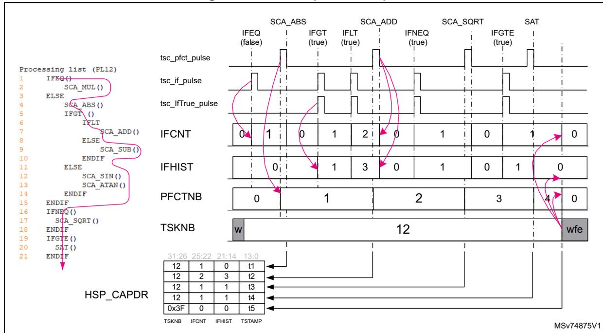
Processing list (PLL2)
1  IFEQ()
2  SCA_MUL()
3  ELSE
4  SCA_ABS()
5  IFGT()
6  IFLT()
7  SCA_ADD()
8  ELSE
9  SCA_SUB()
10 ENDIF
11 ELSE
12 SCA_SIN()
13 SCA_ATAN()
14 ENDIF
15 ENDIF
16 IFNEQ()
17 SCA_SQRT()
18 ENDIF
19 IFGTE()
20 SAT()
21 ENDIF
Signal transitions (SCA_ABS, SCA_ADD, SCA_SQRT, SAT) and register values:
| Signal | IFEQ (false) | IFGT (true) | IFLT (true) | IFNEQ (true) | IFGTE (true) |
|---|---|---|---|---|---|
| tsc_pfc_pulse | High | Low | High | Low | High |
| tsc_if_pulse | High | Low | High | Low | High |
| tsc_ifTrue_pulse | High | Low | High | Low | High |
| IFCNT | 0 | 1 | 0 | 1 | 2 |
| IFHIST | 0 | 1 | 3 | 0 | 1 |
| PFCTNB | 0 | 1 | 2 | 3 | 4 |
| TSKNB | w 12 wfe | ||||
Capture values:
| 31:26 | 25:22 | 21:14 | 13:0 |
|---|---|---|---|
| 12 | 1 | 0 | t1 |
| 12 | 2 | 3 | t2 |
| 12 | 1 | 1 | t3 |
| 12 | 1 | 1 | t4 |
| 0x3F | 0 | 0 | t5 |
TSKNB IFCNT IFHIST TSTAMP
MSV74875V1
If the capture register needs to be written with a new record while the application did not yet read the previous value:
- • The TSC activates the overrun flag (CAPOVRF).
- • The TSC does not overwrite the capture register. The previous unread value is not corrupted.
- • The TSC does not generate a capture event for the TRGO.
The TSC also provides CAPRDYF, asserted when a data is available in the HSP_CAPDR register. This flag is automatically cleared when the CPU reads HSP_CAPDR.
If CAPRDYIE is set in the HSP events interrupt enable register (HSP_EVT_IER) , an interrupt can be generated to the CPU.
Note: A TRGO signal can be generated as well. Depending on the product, it allows using the device DMA to read HSP_CAPDR (see Section 19.4.15: Trigger outputs (TRGO)).
Application example: catching the SPE state in case of SPE break
The application must follow this programming sequence:
- 1. Clear FRCNTEN.
- 2. Clear CAPMOD[1:0].
- 3. In the BKITF, enable all sources that are able to freeze the SPE.
- 4. Set CAPMOD[1:0].
This configuration can be helpful if the application wants to log field issues and identify what the SPE was doing when a break event occurred. The timestamp is not enabled in this example.
Application example: capturing processing function timestamps
The application must follow the programming sequence below:
- • If the application intends to generate capture events only for processing functions located in a specific task:
- a) In the TCU, write the task number where the trace must be done in TSKCMP0[5:0] in the HSP task comparator unit register (HSP_TCUCFGR) .
- b) Enable the task comparator 0 by setting TC0EN in HSP_TCUCFGR.
- c) In BKITF, set TSKFLT.
- • If the application intends to generate capture events every time a new processing function is executed, clear TSKFLT in the BKITF block. It is not necessary to program the TCU block.
- • Prevent the processing function transition detector to break the SPE by setting SSSEN = 0.
- • In the TSC:
- – Clear FRCNTEN.
- – Clear CAPMOD[1:0].
- – Set the PRESC[4:0] to the desired value.
- – Set FRCNTEN.
- – Select the processing functions capture mode (CAPMOD[1:0] = 0b11).
The application can read the captured values in several ways:
- • In polling mode, by waiting for CAPRDYF = 1, then reading HSP_CAPDR. This method is simple but not flexible and requests CPU load.
- • In interrupt mode, by setting CAPRDYIE to allow the HSP to generate an interrupt every time new data are available. This is a simple and flexible method, but requests CPU load.
- • Program the HSP to generate an event on one of the hsp_trgo[x] signals. This can be done by setting TRGO0SRC[1:0] to 3, for example, to use the hsp_trgo_out[3] signal. Depending on the product capabilities, the hsp_trgo[x] signals are connected to the trigger inputs of the device DMA, allowing it to read HSP_CAPDR every time a new timestamp is available. This method is the most efficient for the CPU loading but also for real time.
Note: Performing captures of processing function transitions may cause real-time issues, depending on the traced processing function. The execution time of some processing functions can be down to 10 hsp_hclk_core_ck cycles, causing potential overrun if HSP_CAPDR is not read on time.
Warning: When CAPMOD[1:0] must be modified, it is recommended to clear it before setting it to the desired value.
19.4.17 BRAM conflict counter
The BRAM can be accessed by the following masters:
- • SPE
- • SoC master devices via HSP slave port SP1
The priority is given to the SPE, but the application may want to check if access requests to the BRAM-A, BRAM-B, or BRAM-AB suffer from contentions, reducing the overall performance. For this purpose, the HSP offers a 32-bit conflict counter incremented every time the MMC detects a contention on BRAM access.
This feature can be enabled or disabled through CCNTREN in the HSP capture control register (HSP_CAPCR) . The conflict counter is reset when CCNTREN is disabled.
The conflict counter value can be read at any moment through the HSP conflict counter register (HSP_CCNTR) .
19.4.18 Snoop function (SNOOP)
The HSP offers the possibility to observe key signals to ease application tuning. The application can select which set of signals can be observed on the HSP_SNP[5:0] pads through SNPSELB[2:0] and SNPSEL A[2:0] in the HSP SNOOP register (HSP_SNPR) .
Figure 103. SNOOP function
![Diagram of the SNOOP function showing two 'See table' blocks with 8-bit outputs (0-7) connected to multiplexers. The left multiplexer is controlled by SNPSELB[2:0] and its output is connected to HSP_SNP[5:3]. The right multiplexer is controlled by SNPSEL A[2:0] and its output is connected to HSP_SNP[2:0].](/RM0487-STM32U3/821b2e50841f041c8c6aff81e2f63b9d_img.jpg)
The diagram illustrates the SNOOP function within the HSP. It features two identical 'See table' blocks, each with an 8-bit output (labeled 0 to 7). These outputs are connected to two separate 8-to-3 bit multiplexers. The left multiplexer is controlled by the signal SNPSELB[2:0] and its output is connected to the HSP_SNP[5:3] pads. The right multiplexer is controlled by the signal SNPSEL A[2:0] and its output is connected to the HSP_SNP[2:0] pads. The entire function is labeled 'SNOOP' at the top left. A reference code 'MSV74876V1' is present in the bottom right corner of the diagram.
The table below shows the signal that can be observed through pads.
Table 158. Snoop signal selection
| SNPSELx[2:0] | HSP_SNP[5] | HSP_SNP[4] | HSP_SNP[3] | HSP_SNP[2] | HSP_SNP[1] | HSP_SNP[0] |
|---|---|---|---|---|---|---|
| SNPSELB[2:0] | SNPSELA[2:0] | |||||
| 0 | Disabled | Disabled | Disabled | Disabled | Disabled | Disabled |
| 1 | tsk_active[5] | tsk_active[4] | tsk_active[3] | tsk_active[2] | tsk_active[1] | tsk_active[0] |
| 2 | prc_evt[25] | prc_evt[24] | prc_evt[23] | - | - | - |
| 3 | dcmd_evt | cdeg_evt | hdeg_evt | trgin_evt[0] | buff_evt[0] | adc_evt[0] |
| 4 | tsc_pfctnb[5] | tsc_pfctnb[4] | tsc_pfctnb[3] | tsc_pfctnb[2] | tsc_pfctnb[1] | tsc_pfctnb[0] |
| 5 | - | - | tsk_cmp[3] | tsk_cmp[2] | tsk_cmp[1] | tsk_cmp[0] |
| 6 | tsc_call_pulse | tsc_if_pulse | tsc_iftrue_pulse | evtc_wkup | spe_jump_evt | spe_wfe |
| 7 | pe_evt[5] | pe_evt[4] | pe_evt[3] | pe_evt[2] | pe_evt[1] | pe_evt[0] |
19.4.19 Break interface (BKITF)
The HSP offers a break output interface, providing up to four break output signals ( hsp_brk_out[3:0] ). These signals can be used by the application to stop sensitive peripherals when a critical issue is detected in the HSP.
The HSP also offers a break input interface allowing the application to freeze the SPE in case of internal errors or errors reported by an external block through hsp_break_in . When the SPE breaks, it is possible to store in a capture register which processing list the HSP was executing, as well as a timestamp.
In addition, the BKITF allows the step-by-step processing list execution with the processing function granularity for debugging purposes.
Figure 104. Break interface
![Figure 104. Break interface diagram showing the internal architecture of the HSP break interface. The diagram is divided into two main sections: 'break output interface' and 'break input interface'. In the 'break output interface', error flags from the HITC (HDEGOVRF, FWERRF, ACCERRF, OPCOERRF, FPUERRF, PFCTF[31:28], FPUSATF) are connected to a series of 8-bit wide 'Enable logic' blocks. These blocks are OR-ed together to produce the 'hsp_break_out[3:0]' signal. In the 'break input interface', the 'hsp_break_in' signal is synchronized and passed through a 'BKIN interface' to a series of 8-bit wide 'Enable logic' blocks. These are also OR-ed together to produce a 'bki_brk' signal, which is then passed to a 'BRK_FUNC' block. The 'BRK_FUNC' block outputs a 'brk_o' signal to the 'HITC' (labeled 'BKINF') and 'TSC' (labeled 'tsc_pfctd'). The 'BRK_FUNC' block also outputs a 'bkitf_spfz' signal to the 'SPE' (labeled 'SPE BRKIF'). The 'DBGMCU' (labeled 'dbgmcu_hsp_stp') and 'CTI' (labeled 'CTI(1)') are also connected to the 'BRK_DBG' block. The diagram is labeled 'MSv74877V3' in the bottom right corner.](/RM0487-STM32U3/34efacdbe173f2428fdbaadd8718cea9_img.jpg)
- 1. CTI is not present in all products (see Section 19.3: HSP implementation ).
- 2. hsp_break_in is not always connected; refer to Table 149: HSP break connections for more details.
HSP break output interface
For each break output signal, it is possible to select one or several flags as the source. The table below lists the possible sources for the break output interface. The control bits listed in the table must be set to allow the corresponding flag to generate a break signal.
Table 159. Flags and signal sources for break function
| Source | Description | Control (1) |
|---|---|---|
| ACCERRF | Access error flag | ACCEREN |
| FPUERRF | FPU Computation errors | FPUEREN |
| OPCOERRF | Illegal operating code | OPCEREN |
| PFCTF[31:28] | Flags set by processing function (application dependent) | PFCT[31:28]EN |
| HDEGOVRF | Dedicated software event generator error | HDEGOVEN |
| FWERRF | Firmware errors | FWEREN |
| FPUSATF | FPU saturation flag | FSATEN |
- 1. These bits are in the HSP break output configuration register x (HSP_BKOxCFGGR) .
Note: These flags are asserted by the HSP or firmware code, and cleared by the application (see Table 156: HSP interrupt requests ).
The hsp_break_out[x] signal is set when at least one of the enabled sources is activated, and goes back to 0 when all enabled sources are inactive.
HSP break input interface
The break input interface can be used to:
- • Freeze the SPE
- • Generate capture events to the TSC
The freeze of the SPE can be activated by various sources:
- • Several error status flags
- • A break input signal
- • A start of the end of execution of processing functions
- • A request from the DBGMCU
- • A request from CTI (if available in the product)
Table 160 lists the possible sources for the break input interface. The control bits must be set to allow the corresponding flag to generate a break signal. These control bits are in the HSP break input configuration register (HSP_BKICFGR) .
Note: The BKINF flag is not asserted by all available break sources.
Table 160. Flags and signal sources for break input and debug functions
| Break sources | Description | HSP control (1) | Affected flag | Affected functions |
|---|---|---|---|---|
| ACCERRF | Access error flag | ACCEREN | BKINF | SPE freeze |
| FPUERRF | FPU Computation errors | FPUEREN | ||
| OPCOERRF | Illegal operating code | OPCEREN | ||
| PFCTF[31:28] | Flags set by processing functions | PFCT[31:28]EN | ||
| HDEGOVRF | Dedicated software event generator error | HDEGOVEN | ||
| FWERRF | Firmware errors | FWEREN | ||
| FPUSATF | FPU saturation flag | FSATEN | ||
| tsc_pfctdt | Processing function transition detection | SSEN | ||
| DBGMCU | HSP freeze when CPU breaks | _(2) | - | SPE freeze |
| CTI | CoreSight CTI | - |
- 1. These bits are located in the HSP break input configuration register (HSP_BKICFGR) , except for DBGMCU and CTI sources.
- 2. DBGMCU has a bit to control this function (see the DEBUG section of the reference manual).
The SPE freeze is controlled by the bkitf_spfz signal. When bkitf_spfz is asserted, the SPE immediately stops fetching code and remains frozen. The HSP_CTRL is still
accessible, allowing the application to access all HSP registers and memories (conditioned by the REGLCK bit).
The SPE can resume the execution if all enabled break sources are inactive and the corresponding flags are cleared.
In addition, the moment the SPE is frozen, a capture event is sent to the TSC to store the time-stamp, the task number, and the processing function number.
If the break is generated by BRK_FUNC, the BKINF is asserted as well. As shown in Figure 105 , when the application resets the BKINF flag, if the break condition is still present at the input, the BKINF flag is not reset (#1 in the figure). If the break condition is no longer present, the CPU can clear the BKINF flag, and the SPE can resume the execution (#2 in the figure).
When the SPE is in break, the application can decide on one of the following actions:
- • Resume the SPE execution: the application clears all enabled break sources and clears the BKINF (by setting BKINC).
- • Restart the complete application: the application maintains the SPE frozen by not resetting the BKINF and performs an HSP reset through the RCC control bits.
The break input function is configured through the HSP break input configuration register (HSP_BKICFGR) .
Figure 105. Break input timing example
The diagram shows four signal lines over time:
- brk_o : A pulse signal representing the break input.
- BKINF (bkif_out) : A status flag that goes high when brk_o goes high. It stays high even after brk_o goes low until cleared by the CPU.
- SPE state : Transitions from 'Active' to 'Frozen' when BKINF goes high. It returns to 'Active' only when BKINF is cleared and brk_o is low.
- CPU clears BKINF : Indicates points where the CPU attempts to clear the flag. Point (1) shows an attempt while brk_o is high (unsuccessful reset). Point (2) shows attempts after brk_o is low (successful reset).
19.5 Debug
The HSP offers the following debug options:
- • Freeze the SPE according to some error status flags.
This can be helpful to find the processing function that is causing the error (see Application example: SPE freeze on specific error conditions ). - • Freeze the SPE every time the SPE starts the execution of a new processing function (see Application example: SPE step-by-step debug ).
- • Capture a timestamp every time a new processing function is executed (see Application example: capturing processing function timestamps ).
- • Freeze the SPE when the CPU is halted by using a control bit located in the DBGMCU block.
Application example: SPE freeze on specific error conditions
This feature can be used in applications requesting the SPE to stop immediately in case of errors inside or outside the HSP. It can also be used for debugging purposes, to find the processing function generating an unexpected error, for example.
To use this function, the HSP must be programmed as follows:
- • Define which flags or signals generate an SPE break (see Table 160: Flags and signal sources for break input and debug functions ).
- • If CAPMOD[1:0] of the TSC block is set to 0b01, when the SPE breaks, the application finds the timestamp, the last task, and the processing function number in the HSP_CAPDR register.
When the SPE breaks due to error detection, the application can decide:
- • To resume the SPE execution.
- • To restart the complete application.
Application example: SPE step-by-step debug
This feature can be helpful for debugging purposes to analyze data buffers after the execution of each processing function. It is possible to perform this step-by-step debugging only for processing functions located in a specific task, or for any processing function.
To use this feature, the HSP must be programmed as follows:
- • If the application intends to break the SPE only when a specific task is executed:
- – In the TCU, write the task number where the step-by-step feature must be activated in TSKCMP0[5:0] of the HSP task comparator unit register (HSP_TCUCFGR) and enable the task comparator by setting TC0EN in HSP_TCUCFGR.
- – Set the TSKFLT bit of the HSP_CAPCR register.
- • If the application intends to break the SPE every time a new processing function is executed, clear TSKFLT. No need to program the TCU block.
- • Allows the step-by-step feature to break the SPE by setting SSEN = 1.
- • If the capture mode of the TSC is configured to perform a capture every time the SPE is frozen (CAPMOD[1:0] = 0b01), when the SPE breaks, the application finds the task under execution, the processing function number, and a timestamp in HSP_CAPDR.
When the SPE is in break, the application can check buffer contents and resume the SPE execution. To resume the SPE execution, the application must clear the BKINF flag by setting BKINC in the HSP error interrupt clear register (HSP_ERR_ICR) . If additional flags or signals are able to generate a break, all enabled sources must be cleared to resume the SPE.
The CPU can be broken when the SPE breaks (see Section 19.5.1: Register protection ).
In the figure below, TSKCMP0[5:0] is set to 5. The SPE runs normally until it starts the execution of task number 5. At the start of the execution of task number 5, the SPE breaks, allowing the application to dump the data before execution of processing function number 1. Then the application clears the BKINF flag, and the SPE executes processing function number 1 and breaks again at the start of processing function number 2, allowing the application to dump data, and so on.
Figure 106. Step-by-step timing example
![Timing diagram showing signals: TSFLT, tsk_cmp[0], tsk_active[5:0], SPE state, tsc_pfctnb[5:0], tsc_pfcttd, BKINF, and Clear of BKINF over time. The diagram shows various states like RUN, WFE, and FROZEN for the SPE state, and corresponding values for other signals.](/RM0487-STM32U3/e781ba3bd4acfe316bc8e7729ffc1699_img.jpg)
The timing diagram illustrates the sequence of events for the HSP.
- TSFLT : A signal that goes high (1) at the beginning and remains high.
- tsk_cmp[0] : A signal that goes high when the SPE state transitions to FROZEN and returns low when it transitions back to RUN.
- tsk_active[5:0] : A register value that changes between 0x3F, 2, 5, and 0x3F based on the SPE state.
- SPE state : Transitions between RUN, WFE, and FROZEN states. It starts in RUN, goes to WFE, then RUN, then FROZEN, then RUN, then FROZEN, then RUN, then FROZEN, then RUN, then FROZEN, and finally WFE.
- tsc_pfctnb[5:0] : A register value that changes between 0, 1, 2, and 3 based on the SPE state. It is 0 in RUN/WFE states and increments (1, 2, 3) when in FROZEN states.
- tsc_pfcttd : A signal that pulses high when the SPE state transitions to FROZEN.
- BKINF : A signal that goes high when the SPE state transitions to FROZEN and returns low when it transitions back to RUN.
- Clear of BKINF : A signal that pulses high when the SPE state transitions to RUN.
19.5.1 Register protection
The HSP embeds some hardware protection to prevent unexpected changes to register contents when the HSP is activated. Table 161 shows the list of write-protected and unprotected fields. The register protection is mainly handled by the REGLCK bit.
Note: When the application sets the REGLCK bit, it is no longer possible to clear it by writing this bit to 0. The HSP must be reset.
Table 161. List of locked fields
| Register | Unprotected fields | Write-protected fields | Write protection condition |
|---|---|---|---|
| HSP control register (HSP_CR) | BOOTEN REGLCK RSTREQ SPECGRDIS MMCCGRDIS CTRLGRDIS DCMDEVEN | - | BOOTEN = 1 |
| HSP event enable register (HSP_EVTENR) | - | All | REGLCK = 1 |
| HSP event synchronization enable register (HSP_ESYNCENR) | - | All | REGLCK = 1 |
| HSP event synchronization source register 0 (HSP_ESYNC0SRCR) HSP event synchronization source register 1 (HSP_ESYNC1SRCR) HSP event synchronization source register 2 (HSP_ESYNC2SRCR) | - | All | REGLCK = 1 or EVTENx = 1 |
Table 161. List of locked fields (continued)
| Register | Unprotected fields | Write-protected fields | Write protection condition |
|---|---|---|---|
| HSP event source register 0 (HSP_EVT SRC0R) HSP event source register 1 (HSP_EVT SRC1R) HSP event source register 2 (HSP_EVT SRC2R) | - | All | REGLCK = 1 or EVTENx = 1 |
| HSP BUFF configuration register (HSP_BUFFCFGR) | - | All | REGLCK = 1 |
| HSP BUFF configuration register (HSP_BUFFCFGR) | - | All | REGLCK = 1 or BUFFER = 1 |
| HSP TRGIN configuration register (HSP_TRGINCFGR) HSP TRGIN input selection register 0 (HSP_TRGINSEL0) HSP TRGIN input selection register 1 (HSP_TRGINSEL1) HSP TRGIN input selection register 2 (HSP_TRGINSEL2) | - | All | REGLCK=1 or TRGixEN = 1 |
| HSP TRGO configuration register (HSP_TRGOCFGR) | - | All | REGLCK = 1 or TRGOEN = 1 |
| HSP task comparator unit register (HSP_TCUCFGR) | - | All | REGLCK = 1 |
| HSP task overlap control register (HSP_TOVLPCR) | - | All | REGLCK = 1 |
| HSP break output configuration register x (HSP_BK0xCFGR) | - | All | REGLCK = 1 |
| HSP break input configuration register (HSP_BKICFGR) | - | All | REGLCK = 1 |
19.6 HSP firmware description
The HSP is built around a dedicated high-performance signal processor engine (SPE) running the firmware embedded in the CROM and the CRAM. The CROM mainly contains a set of optimized signal processing functions (libraries), and the CRAM contains the scheduler part of the HSP.
These signal processing functions are called “processing functions”, and the application can record several lists of processing functions to be executed upon activation of specific events. These lists of processing functions are called “processing lists”.
Events generated by peripherals trigger tasks, and each task can contain a single processing list.
This section gives an overview of the way that the application can perform the various operations supported by the HSP, such as running a direct command or recording a processing list.
This document does not provide details on processing functions; refer to the user manual HSP processing functions on STM32 MCUs (UM3360) .
19.6.1 Processing list mapping
Table 162 shows the processing list mapping. Processing lists 0 to 36 are dedicated to recording application processing lists.
Processing lists 37, 38, and 39 are built-in processing lists, not available to the application.
- • The processing list number 37, named PLSUP, is responsible for several control tasks, such as recording processing lists.
- • The processing list number 38, named PLDCMD, is used to run direct commands when the application wants to use the HSP in accelerator mode.
- • The processing list number 39, named PLFAIL, is triggered every time the application tries to execute a processing list with a number higher than 38 or when the application wants to execute a nonexisting processing list.
The built-in processing lists cannot be modified by the application.
After an HSP reset, processing lists 0 to 36 are routed to PLFAIL, to handle the activation of nonexisting processing lists. Every time the application records a new processing list, the link to PLFAIL is replaced by the link to the new processing list.
Several blocks can trigger a processing list: TRGIN, STREAM, CSEG, HSEG, CDEG, HDEG, DCMD.
Table 162 shows that:
- • Processing list number 0 can only be triggered by HDEG.
- • Processing lists numbers 1 to 22 can be triggered by TRGIN, STREAM, CSEG, HSEG, CDEG, and HDEG.
- • Processing lists numbers 23 to 36 can be triggered by CDEG and HDEG
- • Processing list number 37 can be triggered by CDEG.
- • Processing list number 38 can be triggered by DCMD.
CDEG always has the priority 27 (lowest); HDEG always has the priority 0 (highest); DCMD always has the priority 26.
TRGIN, STREAM, CSEG, and HSEG always have the priority of the processing number they are activating. For example, if STREAM is programmed to trigger processing list number 12, then its priority is 12.
Table 162. Processing list mapping
| Peripheral generating events | - | Processing list number | Processing list usage |
|---|---|---|---|
| CDEG, HDEG | → | 0 | Application PL or jump to PLFAIL |
| TRGITF, STREAM, CSEG, HSEG, CDEG, HDEG | → | 1 | Application PL or jump to PLFAIL |
| → | ... | ... | |
| → | 22 | Application PL or jump to PLFAIL | |
| CDEG, HDEG | → | 23 | Application PL or jump to PLFAIL |
| → | ... | ... | |
| → | 36 | Application PL or jump to PLFAIL | |
| CDEG | → | 37 | PLSUP |
| DCMD | → | 38 | PLDCMD |
| - | → | 39 | PLFAIL |
19.6.2 Sending commands to the HSP
The application must send commands to the HSP in the following cases:
- • To complete the HSP initialization phase by sending the FW_INIT command.
- • When a processing list must be programmed.
- • When a direct command must be executed.
- • When the application wants to erase all processing lists.
Sending the FW_INIT command
The firmware initialization command (FW_INIT) is sent only once during the initialization phase to give to the HSP firmware the base address of the BRAMAB, and to activate or not the performance monitor. This base address may differ from a product to another.
To send the FW_INIT command, the application must do the following:
- 1. Wait until the HSP is ready to accept the FW_INIT command, signified by BSTAT[3:0] = 1.
- 2. Send the FW_INIT command as follows:
- a) Check that MSGB is free (C2HSEM is cleared).
- b) Write the base address of BRAM-AB in HSP_PARAMR0. This address changes from one product to another, so the application needs to provide this information to the HSP.
- c) Clear HSP_PARAMR1 to disable the performance monitor, and set it to enable it.
- d) Write the command ID of the FW_INIT command in HSP_C2HMSGDR.
- e) Set C2HSEM.
- 3. Check for the completion of the command execution (H2CSEM is set).
- 4. Read the command status in HSP_H2CMSGDR. If the status differs from 0, the command has not been processed properly.
- 5. Clear H2CSEM.
Sending commands to the supervisor
The PLSUP built-in processing list activates the supervisor function. The supervisor can be used to perform various tasks including the processing list recording. The supervisor can be activated at any moment by writing 37 in the HSP CPU dedicated event generation register (HSP_CDEGR) .
The supervisor event has the lowest priority. If it is activated while other active events are pending, it is served when all other events are served.
To send a command to the supervisor, the application must:
- 1. Activate the supervisor.
- 2. Use the MSGB and HSP_PARAMRx to send commands.
The recommended procedure to send a command to the supervisor is detailed below:
Sending a command to the supervisor
- 1. If not yet enabled, set CDEGEN in the HSP_IFTENR register.
- 2. Activate (if not done yet) the supervisor as follows:
- a) Check that CDEG is free (CDEGBSY is cleared).
- b) Write 37 in the HSP_CDEGR register.
- 3. Check that MSGB is free (C2HSEM is cleared).
- 4. Write the command parameters in the HSP_PARAMRx registers.
- 5. Write the command ID in the HSP_C2HMSGDR register.
- 6. Set C2HSEM in the HSP_C2HSEMR register.
- 7. Wait for the completion of the command execution (H2CSEM is set).
- 8. Read the HSP_H2CMSGDR register to get the command status.
- 9. Clear H2CSEM.
As shown in the figure below, the supervisor can perform the following operations:
- • Erase all existing processing lists.
- • Program new processing lists.
Figure 107. PLSUP simplified algorithm
![Flowchart of the PLSUP simplified algorithm. It starts with 'PLSUP' (Activated by event 37), then checks 'C2HSEM == 1?'. If 'No', it loops back to 'PLSUP'. If 'Yes', it checks 'HSP_C2HMSGDR == PL_RESET?'. If 'Yes', it erases all programmed processing lists and sets various registers. If 'No', it checks 'HSP_C2HMSGDR == PROCFG_START?'. If 'Yes', it sets BSTAT to 3 and starts programming a new processing list. If 'No', it sets FWERRN[9:0] to CMDERR, FWERRF to 1, and C2HSEM to 0. All three paths lead to 'END'.](/RM0487-STM32U3/357ad5e52ef97ded248d6a371333f332_img.jpg)
graph TD; PLSUP[PLSUP] -- "Activated by event 37" --> C2HSEM{C2HSEM == 1?}; C2HSEM -- No --> PLSUP; C2HSEM -- Yes --> HSP_RESET{HSP_C2HMSGDR == PL_RESET?}; HSP_RESET -- Yes --> Erase["Erase all the programmed processing lists<br>Write status into HSP_H2CMSGDR<br>Set C2HSEM to 0<br>Set H2CSEM to 1"]; HSP_RESET -- No --> HSP_START{HSP_C2HMSGDR == PROCFG_START?}; HSP_START -- Yes --> BSTAT3[Set BSTAT to 3]; BSTAT3 -- "Start programming of a new processing list<sup>1</sup>" --> Recording[Processing list recording]; Recording --> BSTAT2[Set BSTAT to 2]; HSP_START -- No --> Error["Set FWERRN[9:0] to CMDERR<br>Set FWERRF to 1"]; Error --> C2HSEM0[Set C2HSEM to 0]; Erase --> END[END]; BSTAT2 --> END; C2HSEM0 --> END;MSv74880V2
1. Refer to Figure 108: Processing list programming algorithm .
19.6.3 Recording processing lists
At any time, the application can add a new processing list to the HSP by activating the supervisor:
- 1. Send the PROCFG_START command as follows:
- a) Activate the supervisor by writing 37 in HSP_CDEGR (this action activates the supervisor, if not done yet).
- b) Check that C2HSEM is cleared.
- c) Write the processing list number in the HSP_PARAMR0 register.
- d) Write the PROCFG_START command ID in the HSP_C2HMSGDR register.
- e) Set C2HSEM in the HSP_C2HSEMR register.
- f) Wait for H2CSEM to be set, read the command status, and clear H2CSEM.
- 2. Send the command to record the first processing function as follows:
- a) Check that C2HSEM is cleared.
- b) Write the processing function parameters in the HSP_PARAMRx registers.
- c) Write the processing function command ID in the HSP_C2HMSGDR register.
- d) Set C2HSEM in the HSP_C2HSEMR register.
- e) Wait for H2CSEM to be set, read the command status, and clear H2CSEM.
- 3. Record the wanted sequence by sending commands as explained in step 2.
- 4. Write the PROCFG_END command to exit the supervisor:
- a) Check that C2HSEM is cleared.
- b) Write the PROCFG_END command ID in the HSP_C2HMSGDR register.
- c) Set C2HSEM in the HSP_C2HSEMR register.
- d) Wait for H2CSEM to be set, read the command status, and clear H2CSEM.
The number and format of each processing function parameter are described in the user manual HSP processing functions on STM32 MCUs (UM3360).
For each command, the HSP firmware sends back a status with HSP_H2CMSGDR.
Figure 108 shows the processing list recording sequence:
- 1. When the PROCFG_START command is recognized, the supervisor enters into this processing list programming sequencer.
- 2. BSTAT[3:0] indicates when the supervisor is programming a processing list.
- 3. When an error is detected, processing list programming is aborted. The processing list address is removed from TSKLUT. The command status reported by the command provides information about the error root cause.
As soon as a processing list is programmed, if its associated event is enabled, activated, and selected by the EVTC, the processing list is executed.
Figure 108. Processing list programming algorithm
graph TD
    Start[Processing list recording] --> ReadParam[Read parameter]
    ReadParam --> Invalid{Parameters invalid?}
    Invalid -- Yes --> CMD_ERR1[CMD_ERR]
    Invalid -- No --> StartList[Start creation of processing list:
TSKLUT updated
Write status into HSP_H2CMMSGDR
Set C2HSEM to 0
Set H2CSEM to 1]
    StartList --> Wait[Wait for new command]
    Wait --> C2HSEM{C2HSEM == 1?}
    C2HSEM -- No --> Wait
    C2HSEM -- Yes --> PROCFG_END{HSP_C2HMSGD = PROCFG_END?}
    PROCFG_END -- Yes --> WriteStatus1[Write status into HSP_H2CMMSGDR
Set H2CSEM to 1
Set C2HSEM to 0]
    WriteStatus1 --> END1[END]
    PROCFG_END -- No --> KnownFunc{HSP_C2HMSGD = known
processing function?}
    KnownFunc -- No --> CMD_ERR2[CMD_ERR]
    KnownFunc -- Yes --> ReadParams[Read parameters]
    ReadParams --> Valid{All parameters valid,
enough memory, etc.?}
    Valid -- No --> CMD_ERR2
    Valid -- Yes --> AddFunc[Add the processing function
to the processing list]
    AddFunc --> Translate[Translate command into efficient executable code into CRAM
Add the parameters into the DRAM
Write status into HSP_H2CMMSGDR
Set C2HSEM to 0
Set H2CSEM to 1]
    Translate --> END2[END]
    CMD_ERR3[CMD_ERR] --> RemoveList[Processing list removed from TSKLUT
Error status written into HSP_H2CMMSGDR
Set C2HSEM to 0
Set H2CSEM to 1]
    RemoveList --> END3[END]
MSV74881V2
19.6.4 Executing direct commands (accelerator mode)
At any time, the application can ask the HSP to execute a processing function as a direct command. If the HSP is executing processing lists, the execution of the direct command is delayed until the EVTTC grants the request.
The direct commands are mainly used to execute processing functions dedicated to vector operations. In addition, the processing functions executed in immediate mode can only work with data from BRAM.
The direct command execution is performed through the DCMD and HSP_PARAMRx registers.
The list below provides the recommended sequence to run a direct command. The number of arguments and pointers depend on the command executed (refer to the HSP firmware commands in the user manual HSP processing functions on STM32 MCUs (UM3360) ).
The DCMD block is enabled by default, but can be disabled:
- 1. Write the command ID of the command to be executed in the HSP DCMD command ID register (HSP_DCMDIDR) .
- 2. Write all parameters except the pointers in HSP_PARAMRx.
- 3. Write the first pointer in HSP_DCMDPTR0.
- 4. Write the second pointer in HSP_DCMDPTR1 (if needed).
- 5. Write the third pointer in HSP_DCMDPTR2 (if needed).
- 6. Write the fourth pointer as follows (if needed):
- a) Wait for PRTF0 = 0.
- b) Write the fourth pointer in HSP_DCMDPTR0.
- 7. Write the fifth pointer as follows (if needed):
- – Wait for PRTF1 = 0.
- – Write the fifth pointer in HSP_DCMDPTR1.
- 8. And so on
- 9. Wait for command completion by checking that DCBSY = 0.
Figure 109 describes the PLDCMD built-in processing function. The SPE is expecting from the CPU to program the HSP as described above. To reduce overhead, the PLDCMD task does not perform a lot of checks. The application must properly program the direct command interface.
Note: ST provides a set of functions making the HSP interface transparent for the user.
Figure 109. Direct command processing list simplified algorithm
graph TD; PLDCMD[PLDCMD] --> Init["DCBSY = 1<br/>Compute NbPtr from HSP_DCMDIDR<br/>CntPtr = 0<br/>xx = 0"]; Init --> CntPtrCheck{CntPtr lower than NbPtr?}; CntPtrCheck -- No --> Execute[Execute command]; Execute --> ExecComp{Execution completed?}; ExecComp -- No --> Execute; ExecComp -- Yes --> SetDCBSY[Set DCBSY to 0]; SetDCBSY --> END[END]; CntPtrCheck -- Yes --> ReadPtr[Read HSP_DCMDPTR[xx]]; ReadPtr --> Translate["Perform address translation of read pointer<br/>Update HSP_SPE_PARAMR[y]"]; Translate --> Increment["xx ++<br/>CntPtr ++"]; Increment --> xxCheck{xx bigger than 2?}; xxCheck -- No --> ReadPtr; xxCheck -- Yes --> ResetXx[xx = 0]; ResetXx --> ReadPtr;The flowchart illustrates the PLDCMD direct command processing list simplified algorithm. It begins with the PLDCMD block, followed by an initialization block where DCBSY is set to 1, NbPtr is computed from HSP_DCMDIDR, CntPtr is set to 0, and xx is set to 0. A decision diamond asks if CntPtr is lower than NbPtr. If No, it proceeds to Execute command, which then leads to a decision diamond asking if Execution is completed. If No, it loops back to Execute command. If Yes, it proceeds to Set DCBSY to 0, which leads to the END block. If Yes, it proceeds to Read HSP_DCMDPTR[xx], which leads to Perform address translation of read pointer and Update HSP_SPE_PARAMR[y]. This leads to a block where xx and CntPtr are incremented. A decision diamond asks if xx is bigger than 2. If No, it loops back to Read HSP_DCMDPTR[xx]. If Yes, it proceeds to xx = 0, which then loops back to Read HSP_DCMDPTR[xx]. The diagram is labeled MSV74882V1 in the bottom right corner.
19.6.5 Data buffer handling
The HSP working buffers are located in the BRAM. Data exchanges between the HSP and the application can use the following interfaces:
- • BRAM-A, BRAM-B, or BRAM-AB
- • STREAM
Depending on the executed processing function, sharing data through the BRAM must be done using the BRAM-AB section or the BRAM-A and BRAM-B sections. Refer to Table 163: List of processing functions for more details.
Using the BRAM-AB section means that the content of BRAM-A must be the same as BRAM-B.
Figure 110. Data sharing models
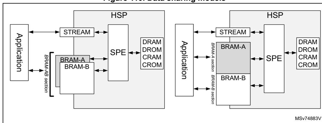
19.6.6 Performance monitoring
In addition to the TSC block, the HSP also offers a performance monitoring tool, allowing the application to measure the execution time of a processing list.
This function is activated by setting the HSP_PARAM1R register (PERFEN) during the execution of the FW_INIT command.
When activated, a cycle counter value can be read in the last DRAM location after the completion of each processing list. The value is given in HSP core clock cycles ( hsp_hclk_core_ck ). Note that the application cannot read this cycle counter if CDRLCK[1:0] is set to 3.
The cycle counter is cleared every time the HSP starts the execution of a processing list.
Note: The PL_RESET command also allows the enabling or disabling of the performance monitor.
19.6.7 Processing functions summary
The table below gives a summary of all commands that the application can use to program processing functions into processing lists, or to execute them as direct commands. All the commands are described in detail in the user manual HSP processing functions on STM32 MCUs (UM3360) .
In the table below:
- • The column “Type” indicates if the function can be executed immediately in accelerator mode (ACC) or included in a processing list (SEQ).
- • The column “STREAM” indicates if input or output data can be taken from the STREAM interface: “Y” = yes, “y/n” = yes for sequencer and no for accelerator mode, “-” means no.
- • The column “BRAM” indicates which BRAM section must be used to exchange data: “DP” means that the BRAM-AB section must be used, “SP” means that the BRAM-A, and/or BRAM-B sections must be used.
Table 163. List of processing functions
| Processing function mnemonic | Description | Type | STREAM | BRAM |
|---|---|---|---|---|
| PROCFG_START | Starts the creation of a processing list | SEQ | - | - |
| PROCFG_END | Ends the creation of a processing list | SEQ | - | - |
| PL_RESET | Processing list reset | SEQ | - | - |
| Filter processing functions on real numbers | ||||
| BIQDF1_CASC | Cascaded biquad direct form 1 filtering | SEQ, ACC | y/n | DP |
| BIQDF2T_CASC | Cascaded biquad direct form 2 transposed filtering | SEQ, ACC | y/n | DP |
| FIR | Optimal FIR filtering | SEQ, ACC | y/n | DP |
| FIRDEC | FIR filtering with decimation | SEQ, ACC | - | DP |
| FIRLMS | FIR filtering with adaptive LMS algorithm | SEQ, ACC | y/n | DP |
| IIRDF1 | Optimal IIR filtering using the direct form 1 | SEQ, ACC | y/n | DP |
| IIR_LATTICE | IIR filtering using the Lattice form | SEQ, ACC | y/n | DP |
| IIR_3P3Z | 3rd order IIR filter with saturation and gain adjust | SEQ | Y | DP |
| IIR_2P2Z | 2nd order IIR filter with saturation and gain adjust | SEQ | Y | DP |
| FLTBANK | Frequency filtering using internal filter banks | SEQ, ACC | - | DP |
| CONV | Convolution between two vectors | SEQ, ACC | - | DP |
| CORR | Correlation between two vectors | SEQ, ACC | - | DP |
| GET_FLTSTATE | Gets the filter state for single stage filters | ACC | - | DP |
| GET_FLTSTATE_BIQ | Gets the filter state for biquads | ACC | - | DP |
| SET_FLTSTATE | Sets the filter state for single stage filters | ACC | - | DP |
| SET_FLTSTATE_BIQ | Sets the filter state for biquads | ACC | - | DP |
| RST_FLTSTATE | Resets the filter state. | ACC | - | - |
| Vector processing functions on real | ||||
| VECT_ABS | Element-wise absolute value | SEQ, ACC | - | DP |
| VECT_ABSMAX | Maximum absolute value of a vector | SEQ, ACC | - | DP |
Table 163. List of processing functions (continued)
| Processing function mnemonic | Description | Type | STREAM | BRAM |
|---|---|---|---|---|
| VECT_ADD | Element-wise addition | SEQ, ACC | - | DP |
| VECT_ATAN2 | Element-wise arc tangent 2 | SEQ, ACC | - | DP |
| VECT_AVG | Average value | SEQ, ACC | - | DP |
| VECT_COPY | Vector copy | SEQ, ACC | - | DP |
| VECT_COS | Element-wise cosine | SEQ, ACC | - | DP |
| VECT_DEC | Vector decimation | SEQ, ACC | - | DP |
| VECT_DIV | Element-wise division | SEQ, ACC | - | DP |
| VECT_DOTP | Dot product | SEQ, ACC | - | DP |
| VECT_EXP | Element-wise exponential | SEQ, ACC | - | DP |
| VECT_EXP10 | Element-wise \( 10^x \) | SEQ, ACC | - | DP |
| VECT_FTOI | Conversion of float32 to 32-bit signed integers | SEQ, ACC | - | DP |
| VECT_FTOU | Conversion of float32 to 32-bit unsigned integers | SEQ, ACC | - | DP |
| VECT_ITOF | Conversion of signed 32-bit integers to float32 | SEQ, ACC | - | DP |
| VECT_I24TOF | Conversion of signed 24-bit integers to float32 | SEQ, ACC | - | DP |
| VECT_Q31TOF | Conversion of signed Q31 to float32 | SEQ, ACC | - | DP |
| VECT_FTOQ31 | Conversion of float32 to signed Q31 | SEQ, ACC | - | DP |
| VECT_LN | Element-wise natural logarithm | SEQ, ACC | - | DP |
| VECT_LOG10 | Element-wise logarithm base 10 | SEQ, ACC | - | DP |
| VECT_MAX | Search for value and position of the biggest element | SEQ, ACC | - | DP |
| VECT_MIN | Search for value and position of the smallest element | SEQ, ACC | - | DP |
| VECT_MUL | Element-wise product | SEQ, ACC | - | DP |
| VECT_MULCOS | Element-wise product with a cosine | SEQ, ACC | - | DP |
| VECT_MULSIN | Element-wise product with a sinus | SEQ, ACC | - | DP |
| VECT_OFFSET | Adds an offset to each element | SEQ, ACC | y/n | DP |
| VECT_OFFSETI | Adds an immediate offset to each element | SEQ, ACC | - | DP |
| VECT_RMS | Root mean square value | SEQ, ACC | y/n | DP |
| VECT_SIN | Element-wise sinus | SEQ, ACC | - | DP |
| VECT_SINCOS | Element-wise sinus and cosine | SEQ, ACC | - | DP |
| VECT_SCALE | Multiplies each element by a value | SEQ, ACC | y/n | DP |
| VECT_SCALEI | Multiplies each element by an immediate value | SEQ, ACC | - | DP |
| VECT_SET | Sets a value to each element | SEQ, ACC | y/n | DP |
Table 163. List of processing functions (continued)
| Processing function mnemonic | Description | Type | STREAM | BRAM |
|---|---|---|---|---|
| VECT_SETI | Sets an immediate value to each element | SEQ, ACC | y/n | DP |
| VECT_SQRT | Element-wise square-root | SEQ, ACC | - | DP |
| VECT_SUB | Element-wise subtraction | SEQ, ACC | - | DP |
| VECT_UTOF | Conversion of unsigned 32-bit integer to float32 | SEQ, ACC | - | DP |
| VECT_ZINS | Interpolation by inserting zeros | SEQ, ACC | - | DP |
| Processing functions operating on complex | ||||
| CMPLX_CONJ | Element-wise conjugate | SEQ, ACC | - | DP |
| CMPLX_DOTP | Dot product | SEQ, ACC | - | DP |
| CMPLX_MAG | Magnitude | SEQ, ACC | - | DP |
| CMPLX_MAGSQR | Magnitude squared | SEQ, ACC | - | DP |
| CMPLX_MUL | Element-wise product | SEQ, ACC | - | DP |
| CMPLX_MULEXP | Element-wise product with an exponential complex | SEQ, ACC | - | DP |
| CMPLX_R MUL | Element-wise product of a complex with a real vector | SEQ, ACC | - | DP |
| CMPLX_FTOQ15 | Conversion of float32 to Q15 format | SEQ, ACC | - | DP |
| CMPLX_Q15TOF | Conversion of Q15 to float32 format | SEQ, ACC | - | DP |
| Scalar processing functions on real | ||||
| SCA_ABS | Absolute value | SEQ | Y | DP |
| SCA_ADD | Addition | SEQ | Y | DP |
| SCA_ATAN2 | Arc tangent 2 | SEQ | Y | DP |
| SCA_CNTCMP | Comparison to a threshold, with a counter | SEQ | - | DP |
| SCA_COS | Cosine | SEQ | Y | DP |
| SCA_CLARKE | Clarke transform | SEQ | - | DP |
| SCA_DIV | Division | SEQ | Y | DP |
| SCA_EXP | Exponential | SEQ | Y | DP |
| SCA_EXP10 | \( 10^x \) | SEQ | Y | DP |
| SCA_FATAN2 | Low-precision Arc tangent 2 | SEQ | Y | DP |
| SCA_FCOS | Low-precision cosine | SEQ | Y | DP |
| SCA_FSIN | Low-precision sinus | SEQ | Y | DP |
| SCA_FTOI | Conversion of a float32 to signed 32-bit integer | SEQ | - | DP |
| SCA_FTOQ31 | Conversion of a float32 to Q31 | SEQ | - | DP |
| SCA_FTOU | Conversion of a float32 to unsigned 32-bit integer | SEQ | - | DP |
Table 163. List of processing functions (continued)
| Processing function mnemonic | Description | Type | STREAM | BRAM |
|---|---|---|---|---|
| SCA_I24TOF | Conversion of a signed 24-bit integer to float32 | SEQ | - | DP |
| SCA_ITOF | Conversion of a signed 32-bit integer to float32 | SEQ | - | DP |
| SCA_Q31TOF | Conversion of a Q31 to float32 | SEQ | - | DP |
| SCA_ICLARKE | Inverses Clarke transform | SEQ | - | DP |
| SCA_IPARK | Inverses Park transform | SEQ | Y | DP |
| SCA_LN | Natural logarithm | SEQ | Y | DP |
| SCA_LOG10 | Logarithm base 10 | SEQ | Y | DP |
| SCA_MUL | Product | SEQ | Y | DP |
| SCA_PARK | Park transform | SEQ | Y | DP |
| SCA_PID | PID operation | SEQ | Y | DP |
| SCA_RAMP | Performs a ramp-up or ramp-down | SEQ | - | DP |
| SCA_SIN | Sinus | SEQ | Y | DP |
| SCA_SINCOS | Sinus and cosine | SEQ | Y | DP |
| SCA_SET | Sets a value | SEQ | Y | DP |
| SCA_SQRT | Square-root | SEQ | Y | DP |
| SCA_SUB | Subtraction | SEQ | Y | DP |
| SCA_TOVECT | Builds a vector with consecutive scalar values | SEQ | Y | DP |
| SCA_UTOF | Conversion of unsigned 32-bit integer into float32 | SEQ | Y | DP |
| Matrix processing functions on real | ||||
| MAT_ABS | Computes the absolute value of each element | SEQ, ACC | - | DP |
| MAT_ADD | Addition of two matrix | SEQ, ACC | - | DP |
| MAT_INV | Computes the inverse of a matrix | SEQ, ACC | - | DP |
| MAT_SUB | The subtraction of two matrix | SEQ, ACC | - | DP |
| MAT_MUL | The product of two matrix | SEQ, ACC | - | DP |
| MAT_OFFSET | Adds an offset to each element of a matrix | SEQ, ACC | y/n | DP |
| MAT_SCALE | Multiplies each element of a matrix by a scalar | SEQ, ACC | y/n | DP |
| MAT_TRANS | Transpose of a matrix | SEQ, ACC | - | DP |
| MAT_VECT2COL | Copies a vector to a matrix column | SEQ, ACC | - | DP |
| MAT_COL2VECT | Copies a matrix column into a vector | SEQ, ACC | - | DP |
| Transform processing functions | ||||
| RFFT | Real FFT transform | SEQ, ACC | - | DP |
| FFT | Complex or real FFT and IFFT transform | SEQ, ACC | - | DP |
| DCT | Discrete cosine transform type 2 | SEQ, ACC | - | DP |
Table 163. List of processing functions (continued)
| Processing function mnemonic | Description | Type | STREAM | BRAM |
|---|---|---|---|---|
| Conditional processing functions | ||||
| IF_ELSE | IF-THEN-ELSE functions | SEQ | - | DP |
| LOOP | Loop function | SEQ | - | DP |
| Convolution processing functions | ||||
| CNN_CONV2D | 2D convolution | ACC | - | SP |
| CNN_CONVVDW | Depth-wise convolution | ACC | - | SP |
| CNN_CONVPW | Point-wise convolution | ACC | - | SP |
| CNN_FC | Fully connected layer | ACC | - | SP |
| CNN_POOL | Pooling layer | ACC | - | SP |
| Specific processing functions | ||||
| COMP | Compares a vector or scalar to two thresholds, and branch according to result. | SEQ | - | DP |
| MUL_WIN | Element-wise product with a window | SEQ | - | DP |
| SAT | Performs a saturation to each vector element, using a programmable MAX and MIN values. | SEQ | - | DP |
| SEND_EVENT | Triggers an event to the SPE. | SEQ | - | - |
| SET_FLAG | Sets flags to generate interrupt to the CPU. | SEQ | - | - |
| SET_GPO | Set GPO signals | SEQ | - | - |
| SET_TRGO | Sets TRGO signals. | SEQ | - | - |
| SET_BITS | Forces a specific field to a value. | SEQ | Y | DP |
| CHK_BITS | Checks values of a bitfield. | SEQ | Y | DP |
| WAIT_COND | Loops until condition is met. | SEQ | Y | DP |
19.7 HSP registers
All HSP registers can be read in 8, 16, or 32 bits. All write operations must be performed in 32 bits.
19.7.1 HSP control register (HSP_CR)
Address offset: 0x000
Reset value: 0x0000 0000
This register is used to control several HSP functions such as HSP boot, register access protection, and smart clock gating.
| 31 | 30 | 29 | 28 | 27 | 26 | 25 | 24 | 23 | 22 | 21 | 20 | 19 | 18 | 17 | 16 |
|---|---|---|---|---|---|---|---|---|---|---|---|---|---|---|---|
| BSTAT[3:0] | Res. | Res. | BARB[1:0] | Res. | Res. | Res. | Res. | Res. | Res. | RSTOK | RSTREQ | ||||
| r | r | r | r | rw | rw | r | rs | ||||||||
| 15 | 14 | 13 | 12 | 11 | 10 | 9 | 8 | 7 | 6 | 5 | 4 | 3 | 2 | 1 | 0 |
| REGLCK | CDRLCK[1:0] | DCMD EVEN | Res. | Res. | Res. | Res. | SPECG DIS | MMCC GDIS | Res. | CTRLC GDIS | Res. | Res. | Res. | BOOTE N | |
| rs | rs | rs | rw | rw | rw | rw | rs | ||||||||
Bits 31:28 BSTAT[3:0] : Boot status
Set and cleared by the HSP. This bitfield shows the status of the boot sequence.
For possible values, refer to Table 151: BSTAT possible values .
Bits 27:26 Reserved, must be kept at reset value.
Bits 25:24 BARB[1:0] : BRAM arbitration
Set and cleared by the CPU.
00: Max arbitration latency is 16 cycles. This setting gives 96% of the BRAM bandwidth to the SPE, when the SPE requests 100% of the BRAM bandwidth. (default after reset).
01: Max arbitration latency is 8 cycles. This setting gives 89% of the BRAM bandwidth to the SPE, when the SPE requests 100% of the BRAM bandwidth.
10: Max arbitration latency is 4 cycles. This setting gives 80% of the BRAM bandwidth to the SPE, when the SPE request 100% of the BRAM bandwidth.
11: Reserved
Note: This bitfield is write-protected when REGLCK = 1.
Bits 23:18 Reserved, must be kept at reset value.
Bit 17 RSTOK : Reset request accepted
Set by the HSP, cleared by hardware when the HSP is reset. This bit indicates to the CPU that the HSP can be safely reset.
0: The HSP is not yet set into a state which ensures a safe reset. The application must wait until this bit is set (default after reset).
1: The HSP can be safely reset.
Bit 16 RSTREQ : Reset request
Set by the CPU, cleared by hardware when the HSP is reset. Writing this bit to 0 has no effect. Read operation returns the effective value.
0: No HSP reset requested (default after reset)
1: HSP reset requested
- Bit 15
REGLCK
: Register write lock access control
Set by the CPU, cleared by hardware when the HSP is reset. Writing this bit to 0 has no effect. Read operation returns the effective value.
0: Registers are accessible by the CPU through the slave AHB interface (default after reset).
1: Selected registers are write-protected and the CPU cannot change the content. - Bits 14:13
CDRLCK[1:0]
: CRAM and DRAM lock access control
Set by the CPU, cleared by hardware when the HSP is reset. Writing this bit to 0 has no effect. Read operation returns the effective value.
00: CRAM and DRAM are accessible for read and write operations (default after reset).
01: CRAM and DRAM are write protected, but can be read.
1x: CRAM and DRAM are read and write protected. - Bit 12
DCMDEVEN
: Direct command event enable
Set and cleared by CPU. This bit is used to enable the generation of an event on hsp_txeu signal every time the execution of a direct command is completed.
0: Event generation disabled (default after reset)
1: Event generation enabled - Bits 11:9 Reserved, must be kept at reset value.
- Bit 8 Reserved, must be kept at reset value.
- Bit 7
SPECGDIS
: SPE clock gating disable
Set and cleared by the CPU.
0: SPE clock gating enabled: SPE clocks are locally gated (default after reset).
1: SPE clock gating disabled: SPE clocks are not locally gated. - Bit 6
MMCCGDIS
: MMC clock gating disable
Set and cleared by the CPU.
0: MMC clock gating enabled: MMC clocks are locally gated (default after reset).
1: MMC clock gating disabled: MMC clocks are not locally gated. - Bit 5 Reserved, must be kept at reset value.
- Bit 4
CTRLCGDIS
: HSP_CTRL clock gating disable
Set and cleared by the CPU.
0: HSP_CTRL clock gating enabled: HSP_CTRL clocks are locally gated (default after reset).
1: HSP_CTRL clock gating disabled: HSP_CTRL clocks are not locally gated. - Bits 3:1 Reserved, must be kept at reset value.
- Bit 0
BOOTEN
: Boot enable control
Set by the CPU and cleared by an HSP reset.
This bit allows the HSP to boot. Writing this bit to 0 has no effect. Read operation returns the effective value.
0: The HSP is not allowed to boot (default after reset).
1: The HSP is allowed to boot, and the SPE executes the code located in the CRAM.
19.7.2 HSP CPU-to-HSP semaphore register (HSP_C2HSEMR)
Address offset: 0x040
Reset value: 0x0000 0000
This register is used by the CPU to synchronize the messages. This register can also be accessed by the SPE processor. When the CPU sets a bit to 1, it sets the corresponding bit. Writing 0 has no effect. Reading returns the effective register value.
| 31 | 30 | 29 | 28 | 27 | 26 | 25 | 24 | 23 | 22 | 21 | 20 | 19 | 18 | 17 | 16 |
|---|---|---|---|---|---|---|---|---|---|---|---|---|---|---|---|
| Res. | Res. | Res. | Res. | Res. | Res. | Res. | Res. | Res. | Res. | Res. | Res. | Res. | Res. | Res. | Res. |
| 15 | 14 | 13 | 12 | 11 | 10 | 9 | 8 | 7 | 6 | 5 | 4 | 3 | 2 | 1 | 0 |
| Res. | Res. | Res. | Res. | Res. | Res. | Res. | Res. | Res. | Res. | Res. | Res. | Res. | Res. | Res. | C2HSEM M |
| rs |
Bits 31:1 Reserved, must be kept at reset value.
Bit 0 C2HSEM : CPU to HSP semaphore
Set by the CPU and cleared by the HSP processor. When the CPU writes this bit to 1, it sets the bit. Writing this bit to 0 has no effect. Reading returns the effective bit value.
0: The CPU to HSP MSGB is ready to send a new message (default after reset).
1: The CPU to HSP MSGB contains a message for the HSP not yet read.
19.7.3 HSP CPU-to-HSP message data register (HSP_C2HMSGDR)
Address offset: 0x044
Reset value: 0x0000 0000
This register is used by the CPU to write a message data for the HSP. Writing this register automatically sets C2HSEM in HSP_C2HSEMR.
| 31 | 30 | 29 | 28 | 27 | 26 | 25 | 24 | 23 | 22 | 21 | 20 | 19 | 18 | 17 | 16 |
|---|---|---|---|---|---|---|---|---|---|---|---|---|---|---|---|
| C2HDATA[31:16] | |||||||||||||||
| rw | rw | rw | rw | rw | rw | rw | rw | rw | rw | rw | rw | rw | rw | rw | rw |
| 15 | 14 | 13 | 12 | 11 | 10 | 9 | 8 | 7 | 6 | 5 | 4 | 3 | 2 | 1 | 0 |
| C2HDATA[15:0] | |||||||||||||||
| rw | rw | rw | rw | rw | rw | rw | rw | rw | rw | rw | rw | rw | rw | rw | rw |
Bits 31:0 C2HDATA[31:0] : CPU message for the HSP
Set and reset by software.
19.7.4 HSP HSP-to-CPU semaphore register (HSP_H2CSEMR)
Address offset: 0x048
Reset value: 0x0000 0000
This register is used by the CPU to synchronize the messages. This register can also be accessed by the HSP processor. When the CPU writes a bit to 1, it clears the corresponding bit. Writing 0 has no effect. Reading returns the effective register value.
| 31 | 30 | 29 | 28 | 27 | 26 | 25 | 24 | 23 | 22 | 21 | 20 | 19 | 18 | 17 | 16 |
|---|---|---|---|---|---|---|---|---|---|---|---|---|---|---|---|
| Res. | Res. | Res. | Res. | Res. | Res. | Res. | Res. | Res. | Res. | Res. | Res. | Res. | Res. | Res. | Res. |
| 15 | 14 | 13 | 12 | 11 | 10 | 9 | 8 | 7 | 6 | 5 | 4 | 3 | 2 | 1 | 0 |
| Res. | Res. | Res. | Res. | Res. | Res. | Res. | Res. | Res. | Res. | Res. | Res. | Res. | Res. | Res. | H2CSEM rc_w1 |
Bits 31:1 Reserved, must be kept at reset value.
Bit 0 H2CSEM : HSP to CPU semaphore
Set by the HSP processor, and cleared by the CPU. When the CPU writes this bit to 1, it clears the bit. Writing this bit to 0 has no effect. Reading returns the effective bit value.
0: The HSP to CPU MSGB does not contain a new message from the HSP (default after reset).
1: The HSP to CPU MSGB contains a new message from the HSP.
19.7.5 HSP HSP-to-CPU message data register (HSP_H2CMMSGDR)
Address offset: 0x04C
Reset value: 0x0000 0000
This register is used by the CPU to read a message data sent by the HSP.
| 31 | 30 | 29 | 28 | 27 | 26 | 25 | 24 | 23 | 22 | 21 | 20 | 19 | 18 | 17 | 16 |
|---|---|---|---|---|---|---|---|---|---|---|---|---|---|---|---|
| H2CDATA[31:16] | |||||||||||||||
| r | r | r | r | r | r | r | r | r | r | r | r | r | r | r | r |
| 15 | 14 | 13 | 12 | 11 | 10 | 9 | 8 | 7 | 6 | 5 | 4 | 3 | 2 | 1 | 0 |
| H2CDATA[15:0] | |||||||||||||||
| r | r | r | r | r | r | r | r | r | r | r | r | r | r | r | r |
Bits 31:0 H2CDATA[31:0] : HSP message for the CPU
Set and reset by software.
19.7.6 HSP DCMD command status register (HSP_DCMDSDR)
Address offset: 0x058
Reset value: 0x0000 0000
This register is used by the CPU to check if the current direct command execution is completed.
| 31 | 30 | 29 | 28 | 27 | 26 | 25 | 24 | 23 | 22 | 21 | 20 | 19 | 18 | 17 | 16 |
|---|---|---|---|---|---|---|---|---|---|---|---|---|---|---|---|
| Res. | Res. | Res. | Res. | Res. | Res. | Res. | Res. | Res. | Res. | Res. | Res. | Res. | Res. | Res. | Res. |
| 15 | 14 | 13 | 12 | 11 | 10 | 9 | 8 | 7 | 6 | 5 | 4 | 3 | 2 | 1 | 0 |
| Res. | Res. | Res. | Res. | Res. | Res. | Res. | Res. | Res. | Res. | Res. | Res. | Res. | Res. | Res. | DCBSY |
| r |
Bits 31:1 Reserved, must be kept at reset value.
Bit 0 DCBSY : Direct command busy flag
Set by hardware and reset by SPE. This flag indicates if the SPE is ready to accept a new MSGD.
0: The current direct command execution is completed. A new CMDID can be written in HSP_DCMDIDR (default after reset).
1: The current direct command execution is ongoing.
19.7.7 HSP DCMD pointer status register (HSP_DCMDPTSR)
Address offset: 0x05C
Reset value: 0x0000 0000
This register is used by the CPU to check if the HSP_DCMDPTRx pointer registers have been read by the SPE.
| 31 | 30 | 29 | 28 | 27 | 26 | 25 | 24 | 23 | 22 | 21 | 20 | 19 | 18 | 17 | 16 |
|---|---|---|---|---|---|---|---|---|---|---|---|---|---|---|---|
| Res. | Res. | Res. | Res. | Res. | Res. | Res. | Res. | Res. | Res. | Res. | Res. | Res. | Res. | Res. | Res. |
| 15 | 14 | 13 | 12 | 11 | 10 | 9 | 8 | 7 | 6 | 5 | 4 | 3 | 2 | 1 | 0 |
| RDOG | Res. | Res. | Res. | Res. | Res. | Res. | Res. | Res. | Res. | Res. | Res. | Res. | PTRF2 | PTRF1 | PTRF0 |
| r | r | r | r |
Bits 31:16 Reserved, must be kept at reset value.
Bit 15 RDOG : Read ongoing indicator
Set and cleared by hardware. This flag indicates if the SPE is currently reading one of the data pointer. The level of this flag can change very fast. It can be used during the debug phase. For example, when the execution of a direct command is abnormally long: if RDOG is stable at 1, it means that the SPE is blocked on the reading of a data pointer. Typically this issue appears when the application did not respect the expected data format for a direct command.
0: SPE does not read a pointer (default after reset).
1: SPE is reading a pointer. The SPE may be blocked if no pointer is provided by the CPU.
Bits 14:3 Reserved, must be kept at reset value.
Bit 2 PTRF2 : Address pointer 2 flag
Set and cleared by hardware. This flag indicates if the SPE read the last address pointer 2 written by the CPU in HSP_DCMDPTR2.
0: SPE read the address pointer 2. A new address pointer can be written in HSP_DCMDPTR2 (default after reset).
1: The current address pointer 2 has not been read by the SPE.
Bit 1 PTRF1 : Address pointer 1 flag
Set and cleared by hardware. This flag indicates if the SPE read the last address pointer 1 written by the CPU in HSP_DCMDPTR1.
0: SPE read the address pointer 1. A new address pointer can be written in HSP_DCMDPTR1 (default after reset).
1: The current address pointer 1 has not been read by the SPE.
Bit 0 PTRF0 : Address pointer 0 flag
Set and cleared by hardware. This flag indicates if the SPE read the last address pointer 0 written by the CPU in HSP_DCMDPTR0.
0: SPE read the address pointer 0. A new address pointer can be written in HSP_DCMDPTR0 (default after reset).
1: The current address pointer 0 has not been read by the SPE.
19.7.8 HSP DCMD command ID register (HSP_DCMDIDR)
Address offset: 0x060
Reset value: 0x0000 0000
This register is used by the CPU to provide the command ID to be executed to the direct command interface (DCMD).
| 31 | 30 | 29 | 28 | 27 | 26 | 25 | 24 | 23 | 22 | 21 | 20 | 19 | 18 | 17 | 16 |
|---|---|---|---|---|---|---|---|---|---|---|---|---|---|---|---|
| Res. | Res. | Res. | Res. | Res. | Res. | Res. | Res. | Res. | Res. | Res. | Res. | Res. | Res. | Res. | Res. |
| 15 | 14 | 13 | 12 | 11 | 10 | 9 | 8 | 7 | 6 | 5 | 4 | 3 | 2 | 1 | 0 |
| CMDID[15:0] | |||||||||||||||
| rw | rw | rw | rw | rw | rw | rw | rw | rw | rw | rw | rw | rw | rw | rw | rw |
Bits 31:16 Reserved, must be kept at reset value.
Bits 15:0 CMDID[15:0] : Command ID
Set and reset by software. This value represents the command ID of the command to be executed.
19.7.9 HSP DCMD address pointer register x (HSP_DCMDPTRx)
Address offset: 0x064 + 0x4 * x, (x = 0 to 2)
Reset value: 0x0000 0000
This register is used by the CPU to provide the address pointers to the DCMD.
| 31 | 30 | 29 | 28 | 27 | 26 | 25 | 24 | 23 | 22 | 21 | 20 | 19 | 18 | 17 | 16 |
|---|---|---|---|---|---|---|---|---|---|---|---|---|---|---|---|
| PTCPU[31:16] | |||||||||||||||
| rw | rw | rw | rw | rw | rw | rw | rw | rw | rw | rw | rw | rw | rw | rw | rw |
| 15 | 14 | 13 | 12 | 11 | 10 | 9 | 8 | 7 | 6 | 5 | 4 | 3 | 2 | 1 | 0 |
| PTCPU[15:0] | |||||||||||||||
| rw | rw | rw | rw | rw | rw | rw | rw | rw | rw | rw | rw | rw | rw | rw | rw |
Bits 31:0 PTCPU[31:0] : Address pointer value
Set and cleared by CPU. The CPU writes in this bitfield the pointer value requested by direct commands. This pointer value represents a peripheral or memory buffer address 'seen' by the CPU. This pointer value is automatically translated into a value directly usable by the SPE.
When the CPU writes this register, the corresponding PTRFx flag is set.
19.7.10 HSP event enable register (HSP_EVTENR)
Address offset: 0x080
Reset value: 0x0000 0000
This register is used to control the generation of events, which trigger a task. Write access operations in this register are not allowed when REGLCK is set.
| 31 | 30 | 29 | 28 | 27 | 26 | 25 | 24 | 23 | 22 | 21 | 20 | 19 | 18 | 17 | 16 |
|---|---|---|---|---|---|---|---|---|---|---|---|---|---|---|---|
| Res. | Res. | Res. | Res. | Res. | Res. | Res. | Res. | Res. | EVTEN[22:16] | ||||||
| rw | rw | rw | rw | rw | rw | rw | |||||||||
| 15 | 14 | 13 | 12 | 11 | 10 | 9 | 8 | 7 | 6 | 5 | 4 | 3 | 2 | 1 | 0 |
| EVTEN[15:1] | Res. | ||||||||||||||
| rw | rw | rw | rw | rw | rw | rw | rw | rw | rw | rw | rw | rw | rw | rw | |
Bits 31:23 Reserved, must be kept at reset value.
Bits 22:1 EVTEN[22:1] : Events enable
Set and reset by software. EVTEN[n] controls the enabling/disabling of the event number n.
0: Event generation disabled (default after reset)
1: Event generation enabled
Note: This bitfield is write-protected when REGLCK = 1.
Bit 0 Reserved, must be kept at reset value.
19.7.11 HSP event synchronization enable register (HSP_ESYNCENR)
Address offset: 0x084
Reset value: 0x0000 0000
This register is used to enable or disable the synchronization mechanism for the event generation. Write access operations to this register are not allowed when REGLCK is set.
| 31 | 30 | 29 | 28 | 27 | 26 | 25 | 24 | 23 | 22 | 21 | 20 | 19 | 18 | 17 | 16 |
| Res. | Res. | Res. | Res. | Res. | CDEG SYNCEN N | Res. | Res. | Res. | EVTSYNCEN[22:16] | ||||||
| rw | rw | rw | rw | rw | rw | rw | rw | ||||||||
| 15 | 14 | 13 | 12 | 11 | 10 | 9 | 8 | 7 | 6 | 5 | 4 | 3 | 2 | 1 | 0 |
| EVTSYNCEN[15:1] | Res. | ||||||||||||||
| rw | rw | rw | rw | rw | rw | rw | rw | rw | rw | rw | rw | rw | rw | rw | |
Bits 31:27 Reserved, must be kept at reset value.
Bit 26 CDEGSYNCEN : CPU dedicated event synchronization enable
Set and cleared by software. This bit controls the enable/disable of the synchronization for the CPU dedicated event.
0: Synchronization disabled (default after reset)
1: Synchronization enabled.
Note: This bit is write-protected when REGLCK = 1.
Bits 25:23 Reserved, must be kept at reset value.
Bits 22:1 EVTSYNCEN[22:1] : Event synchronization enable
Set and cleared by software. EVTSYNCEN[n] controls the enable/disable of the synchronization for the event n.
0: Synchronization disabled (default after reset)
1: Synchronization enabled.
Note: This bitfield is write-protected when REGLCK = 1.
Bit 0 Reserved, must be kept at reset value.
19.7.12 HSP event synchronization source register 0 (HSP_ESYNC0SRCR)
Address offset: 0x088
Reset value: 0x0000 0000
This register is used to select the synchronization source for events 1 to 8. Write access operations to this register are not allowed when REGLCK is set, or when the corresponding EVTENx is set.
| 31 | 30 | 29 | 28 | 27 | 26 | 25 | 24 | 23 | 22 | 21 | 20 | 19 | 18 | 17 | 16 |
| Res. | Res. | EV8SSRC[1:0] | Res. | Res. | EV7SSRC[1:0] | Res. | Res. | EV6SSRC[1:0] | Res. | Res. | EV5SSRC[1:0] | ||||
| rw | rw | rw | rw | rw | rw | rw | rw | ||||||||
| 15 | 14 | 13 | 12 | 11 | 10 | 9 | 8 | 7 | 6 | 5 | 4 | 3 | 2 | 1 | 0 |
| Res. | Res. | EV4SSRC[1:0] | Res. | Res. | EV3SSRC[1:0] | Res. | Res. | EV2SSRC[1:0] | Res. | Res. | EV1SSRC[1:0] | ||||
| rw | rw | rw | rw | rw | rw | rw | rw | ||||||||
Bits 31:30 Reserved, must be kept at reset value.
Bits 29:28 EV8SSRC[1:0] : Event 8 synchronization source
Set and cleared by software.
00: tsk_cmp[0] selected as synchronization source
01: tsk_cmp[1] selected as synchronization source
10: tsk_cmp[2] selected as synchronization source
11: tsk_cmp[3] selected as synchronization source
Note: This bitfield is write-protected when REGLCK = 1 or when EVTEN[8] = 1.
Bits 27:26 Reserved, must be kept at reset value.
Bits 25:24 EV7SSRC[1:0] : Event 7 synchronization source
Set and cleared by software.
00: tsk_cmp[0] selected as synchronization source
01: tsk_cmp[1] selected as synchronization source
10: tsk_cmp[2] selected as synchronization source
11: tsk_cmp[3] selected as synchronization source
Note: This bitfield is write-protected when REGLCK = 1 or when EVTEN[7] = 1.
Bits 23:22 Reserved, must be kept at reset value.
Bits 21:20 EV6SSRC[1:0] : Event 6 synchronization source
Set and cleared by software.
00: tsk_cmp[0] selected as synchronization source
01: tsk_cmp[1] selected as synchronization source
10: tsk_cmp[2] selected as synchronization source
11: tsk_cmp[3] selected as synchronization source
Note: This bitfield is write-protected when REGLCK = 1 or when EVTEN[6] = 1.
Bits 19:18 Reserved, must be kept at reset value.
Bits 17:16 EV5SSRC[1:0] : Event 5 synchronization source
Set and cleared by software.
00: tsk_cmp[0] selected as synchronization source
01: tsk_cmp[1] selected as synchronization source
10: tsk_cmp[2] selected as synchronization source
11: tsk_cmp[3] selected as synchronization source
Note: This bitfield is write-protected when REGLCK = 1 or when EVTEN[5] = 1.
Bits 15:14 Reserved, must be kept at reset value.
Bits 13:12 EV4SSRC[1:0] : Event 4 synchronization source
Set and cleared by software.
00: tsk_cmp[0] selected as synchronization source
01: tsk_cmp[1] selected as synchronization source
10: tsk_cmp[2] selected as synchronization source
11: tsk_cmp[3] selected as synchronization source
Note: This bitfield is write-protected when REGLCK = 1 or when EVTEN[4] = 1.
Bits 11:10 Reserved, must be kept at reset value.
Bits 9:8 EV3SSRC[1:0] : Event 3 synchronization source
Set and cleared by software.
00: tsk_cmp[0] selected as synchronization source
01: tsk_cmp[1] selected as synchronization source
10: tsk_cmp[2] selected as synchronization source
11: tsk_cmp[3] selected as synchronization source
Note: This bitfield is write-protected when REGLCK = 1 or when EVTEN[8] = 1.
Bits 7:6 Reserved, must be kept at reset value.
Bits 5:4 EV2SSRC[1:0] : Event 2 synchronization source
Set and cleared by software.
00: tsk_cmp[0] selected as synchronization source
01: tsk_cmp[1] selected as synchronization source
10: tsk_cmp[2] selected as synchronization source
11: tsk_cmp[3] selected as synchronization source
Note: This bitfield is write-protected when REGLCK = 1 or when EVTEN[2] = 1.
Bits 3:2 Reserved, must be kept at reset value.
Bits 1:0 EV1SSRC[1:0] : Event 1 synchronization source
Set and cleared by software.
00: tsk_cmp[0] selected as synchronization source
01: tsk_cmp[1] selected as synchronization source
10: tsk_cmp[2] selected as synchronization source
11: tsk_cmp[3] selected as synchronization source
Note: This bitfield is write-protected when REGLCK = 1 or when EVTEN[1] = 1.
19.7.13 HSP event synchronization source register 1 (HSP_ESYNC1SRCR)
Address offset: 0x08C
Reset value: 0x0000 0000
This register is used to select the synchronization source for events 9 to 16. Write access operations to this register are not allowed when REGLCK is set, or when the corresponding EVTENx is set.
| 31 | 30 | 29 | 28 | 27 | 26 | 25 | 24 | 23 | 22 | 21 | 20 | 19 | 18 | 17 | 16 |
|---|---|---|---|---|---|---|---|---|---|---|---|---|---|---|---|
| Res. | Res. | EV16SSRC[1:0] | Res. | Res. | EV15SSRC[1:0] | Res. | Res. | EV14SSRC[1:0] | Res. | Res. | EV13SSRC[1:0] | ||||
| rw | rw | rw | rw | rw | rw | rw | rw | ||||||||
| 15 | 14 | 13 | 12 | 11 | 10 | 9 | 8 | 7 | 6 | 5 | 4 | 3 | 2 | 1 | 0 |
| Res. | Res. | EV12SSRC[1:0] | Res. | Res. | EV11SSRC[1:0] | Res. | Res. | EV10SSRC[1:0] | Res. | Res. | EV9SSRC[1:0] | ||||
| rw | rw | rw | rw | rw | rw | rw | rw |
Bits 31:30 Reserved, must be kept at reset value.
Bits 29:28 EV16SSRC[1:0] : Event 16 synchronization source
Set and cleared by software.
00: tsk_cmp[0] selected as synchronization source
01: tsk_cmp[1] selected as synchronization source
10: tsk_cmp[2] selected as synchronization source
11: tsk_cmp[3] selected as synchronization source
Note: This bitfield is write-protected when REGLCK = 1 or when EVTEN[16] = 1.
Bits 27:26 Reserved, must be kept at reset value.
Bits 25:24 EV15SSRC[1:0] : Event 15 synchronization source
Set and cleared by software.
00: tsk_cmp[0] selected as synchronization source
01: tsk_cmp[1] selected as synchronization source
10: tsk_cmp[2] selected as synchronization source
11: tsk_cmp[3] selected as synchronization source
Note: This bitfield is write-protected when REGLCK = 1 or when EVTEN[15] = 1.
Bits 23:22 Reserved, must be kept at reset value.
Bits 21:20 EV14SSRC[1:0] : Event 14 synchronization source
Set and cleared by software.
00: tsk_cmp[0] selected as synchronization source
01: tsk_cmp[1] selected as synchronization source
10: tsk_cmp[2] selected as synchronization source
11: tsk_cmp[3] selected as synchronization source
Note: This bitfield is write-protected when REGLCK = 1 or when EVTEN[14] = 1.
Bits 19:18 Reserved, must be kept at reset value.
Bits 17:16 EV13SSRC[1:0] : Event 13 synchronization source
Set and cleared by software.
00: tsk_cmp[0] selected as synchronization source
01: tsk_cmp[1] selected as synchronization source
10: tsk_cmp[2] selected as synchronization source
11: tsk_cmp[3] selected as synchronization source
Note: This bitfield is write-protected when REGLCK = 1 or when EVTEN[13] = 1.
Bits 15:14 Reserved, must be kept at reset value.
Bits 13:12 EV12SSRC[1:0] : Event 12 synchronization source
Set and cleared by software.
00: tsk_cmp[0] selected as synchronization source
01: tsk_cmp[1] selected as synchronization source
10: tsk_cmp[2] selected as synchronization source
11: tsk_cmp[3] selected as synchronization source
Note: This bitfield is write-protected when REGLCK = 1 or when EVTEN[12] = 1.
Bits 11:10 Reserved, must be kept at reset value.
Bits 9:8 EV11SSRC[1:0] : Event 11 synchronization source
Set and cleared by software.
00: tsk_cmp[0] selected as synchronization source
01: tsk_cmp[1] selected as synchronization source
10: tsk_cmp[2] selected as synchronization source
11: tsk_cmp[3] selected as synchronization source
Note: This bitfield is write-protected when REGLCK = 1 or when EVTEN[11] = 1.
Bits 7:6 Reserved, must be kept at reset value.
Bits 5:4 EV10SSRC[1:0] : Event 10 synchronization source
Set and cleared by software.
00: tsk_cmp[0] selected as synchronization source
01: tsk_cmp[1] selected as synchronization source
10: tsk_cmp[2] selected as synchronization source
11: tsk_cmp[3] selected as synchronization source
Note: This bitfield is write-protected when REGLCK = 1 or when EVTEN[10] = 1.
Bits 3:2 Reserved, must be kept at reset value.
Bits 1:0 EV9SSRC[1:0] : Event 9 synchronization source
Set and cleared by software.
00: tsk_cmp[0] selected as synchronization source
01: tsk_cmp[1] selected as synchronization source
10: tsk_cmp[2] selected as synchronization source
11: tsk_cmp[3] selected as synchronization source
Note: This bitfield is write-protected when REGLCK = 1 or when EVTEN[9] = 1.
19.7.14 HSP event synchronization source register 2 (HSP_ESYNC2SRCR)
Address offset: 0x090
Reset value: 0x0000 0000
This register is used to select the synchronization source for events 17 to 22 and 27. Write access operations to this register are not allowed when REGLCK is set or when the corresponding EVTENx = 1.
| 31 | 30 | 29 | 28 | 27 | 26 | 25 | 24 | 23 | 22 | 21 | 20 | 19 | 18 | 17 | 16 |
|---|---|---|---|---|---|---|---|---|---|---|---|---|---|---|---|
| CDEGSSRC[1:0] | Res. | Res. | Res. | Res. | Res. | Res. | Res. | Res. | EV22SSRC[1:0] | Res. | Res. | EV21SSRC[1:0] | |||
| rw | rw | rw | rw | rw | rw | ||||||||||
| 15 | 14 | 13 | 12 | 11 | 10 | 9 | 8 | 7 | 6 | 5 | 4 | 3 | 2 | 1 | 0 |
| Res. | EV20SSRC[1:0] | Res. | Res. | EV19SSRC[1:0] | Res. | Res. | EV18SSRC[1:0] | Res. | Res. | EV17SSRC[1:0] | |||||
| rw | rw | rw | rw | rw | rw | rw | rw | ||||||||
Bits 31:30 CDEGSSRC[1:0] : CPU dedicated event synchronization source
Set and cleared by software.
00: tsk_cmp[0] selected as synchronization source
01: tsk_cmp[1] selected as synchronization source
10: tsk_cmp[2] selected as synchronization source
11: tsk_cmp[3] selected as synchronization source
Note: This bitfield is write-protected when REGLCK = 1 or when CDEGEN = 1.
Bits 29:22 Reserved, must be kept at reset value.
Bits 21:20 EV22SSRC[1:0] : Event 22 synchronization source
Set and cleared by software.
00: tsk_cmp[0] selected as synchronization source
01: tsk_cmp[1] selected as synchronization source
10: tsk_cmp[2] selected as synchronization source
11: tsk_cmp[3] selected as synchronization source
Note: This bitfield is write-protected when REGLCK = 1 or when EVTEN[22] = 1.
Bits 19:18 Reserved, must be kept at reset value.
Bits 17:16 EV21SSRC[1:0] : Event 21 synchronization source
Set and cleared by software.
00: tsk_cmp[0] selected as synchronization source
01: tsk_cmp[1] selected as synchronization source
10: tsk_cmp[2] selected as synchronization source
11: tsk_cmp[3] selected as synchronization source
Note: This bitfield is write-protected when REGLCK = 1 or when EVTEN[21] = 1.
Bits 15:14 Reserved, must be kept at reset value.
Bits 13:12 EV20SSRC[1:0] : Event 20 synchronization source
Set and cleared by software.
00: tsk_cmp[0] selected as synchronization source
01: tsk_cmp[1] selected as synchronization source
10: tsk_cmp[2] selected as synchronization source
11: tsk_cmp[3] selected as synchronization source
Note: This bitfield is write-protected when REGLCK = 1 or when EVTEN[20] = 1.
Bits 11:10 Reserved, must be kept at reset value.
Bits 9:8 EV19SSRC[1:0] : Event 19 synchronization source
Set and cleared by software.
00: tsk_cmp[0] selected as synchronization source
01: tsk_cmp[1] selected as synchronization source
10: tsk_cmp[2] selected as synchronization source
11: tsk_cmp[3] selected as synchronization source
Note: This bitfield is write-protected when REGLCK = 1 or when EVTEN[19] = 1.
Bits 7:6 Reserved, must be kept at reset value.
Bits 5:4 EV18SSRC[1:0] : Event 18 synchronization source
Set and cleared by software.
00: tsk_cmp[0] selected as synchronization source
01: tsk_cmp[1] selected as synchronization source
10: tsk_cmp[2] selected as synchronization source
11: tsk_cmp[3] selected as synchronization source
Note: This bitfield is write-protected when REGLCK = 1 or when EVTEN[18] = 1.
Bits 3:2 Reserved, must be kept at reset value.
Bits 1:0 EV17SSRC[1:0] : Event 17 synchronization source
Set and cleared by software.
00: tsk_cmp[0] selected as synchronization source
01: tsk_cmp[1] selected as synchronization source
10: tsk_cmp[2] selected as synchronization source
11: tsk_cmp[3] selected as synchronization source
Note: This bitfield is write-protected when REGLCK = 1 or when EVTEN[17] = 1.
19.7.15 HSP pending event level register (HSP_PEVTLR)
Address offset: 0x098
Reset value: 0x0000 0000
This register shows event states before the priority encoder. This register is mainly dedicated to debugging purposes.
| 31 | 30 | 29 | 28 | 27 | 26 | 25 | 24 | 23 | 22 | 21 | 20 | 19 | 18 | 17 | 16 |
|---|---|---|---|---|---|---|---|---|---|---|---|---|---|---|---|
| Res. | Res. | Res. | Res. | EVTL[27:16] | |||||||||||
| r | r | r | r | r | r | r | r | r | r | r | r | ||||
| 15 | 14 | 13 | 12 | 11 | 10 | 9 | 8 | 7 | 6 | 5 | 4 | 3 | 2 | 1 | 0 |
| EVTL[15:0] | |||||||||||||||
| r | r | r | r | r | r | r | r | r | r | r | r | r | r | r | r |
Bits 31:28 Reserved, must be kept at reset value.
Bits 27:0 EVTL[27:0] : Event level
Set and cleared by hardware. This bitfield shows the current events level. Bit n correspond to event n.
0: Level low (inactive)
1: Level high (pending)
19.7.16 HSP interface enable register (HSP_ITFENR)
Address offset: 0x0A0
Reset value: 0x0000 0000
This register is used by the application to enable the STREAM and TRGITF peripheral interfaces. CPU write access operations to this register are not allowed when REGLCK is set. This register can also be modified by the SPE.
| 31 | 30 | 29 | 28 | 27 | 26 | 25 | 24 | 23 | 22 | 21 | 20 | 19 | 18 | 17 | 16 |
|---|---|---|---|---|---|---|---|---|---|---|---|---|---|---|---|
| HDEG EN | HSEGE N | CDEG EN | CSEGE N | DCMD DIS | Res. | TRGI9 EN | TRGI8 EN | TRGI7 EN | TRGI6 EN | TRGI5 EN | TRGI4 EN | TRGI3 EN | TRGI2 EN | TRGI1 EN | TRGI0 EN |
| r | r | rw | rw | rwo | rw | rw | rw | rw | rw | rw | rw | rw | rw | rw | |
| 15 | 14 | 13 | 12 | 11 | 10 | 9 | 8 | 7 | 6 | 5 | 4 | 3 | 2 | 1 | 0 |
| Res. | Res. | Res. | TRGO EN | Res. | Res. | Res. | STREA MEN | Res. | Res. | Res. | Res. | Res. | Res. | Res. | Res. |
| rw | rw |
Bit 31 HDEGEN : HDEG interface enable bit
Set and cleared by software.
0: HDEG interface disabled, and maintained in reset
1: HDEG interface enabled
Bit 30 HSEGEN : HSEG interface enable bit
Set and cleared by software.
0: HSEG interface disabled, and maintained in reset
1: HSEG interface enabled
- Bit 29
CDEGEN
: CDEG interface enable bit
Set and cleared by software.
0: CDEG interface disabled, and maintained in reset
1: CDEG interface enabled
Note: This bit is write-protected when REGLCK = 1. - Bit 28
CSEGEN
: CSEG interface enable bit
Set and cleared by software.
0: CSEG interface disabled, and maintained in reset
1: CSEG interface is enabled
Note: This bit is write-protected when REGLCK = 1. - Bit 27
DCMDDIS
: Direct command interface disable bit
Set and cleared by software. This bit can only be written once, after a HSP reset. By default the direct command interface is enabled. Reading returns the effective value.
0: Writing this bit to 0 enables the DCMD interface, and prevents other applications to disable it (default after reset).
1: Writing this bit to 1 disables the DCMD interface. Only an HSP reset can re enable it.
Note: This bit is write-protected when REGLCK = 1. - Bit 26 Reserved, must be kept at reset value.
- Bits 25:16
TRGINxEN
: TRGINx enable bit (x = 9 to 0)
Set and cleared by software.
0: TRGINx disabled, all the TRGIN logic maintained in reset
1: TRGINx enabled
Note: This bit is write-protected when REGLCK = 1. - Bits 15:13 Reserved, must be kept at reset value.
- Bit 12
TRGOEN
: TRGO enable bit
Set and cleared by software.
0: TRGO function disabled. It is not possible to generate trigger pulses on hsp_trgo[3:0], nor to change the level of hsp_gpo[7:0].
1: TRGO function enabled
Note: This bit is write-protected when REGLCK = 1. - Bits 11:9 Reserved, must be kept at reset value.
- Bit 8
STREAMEN
: STREAM enable
Set and cleared by software.
0: STREAM disabled
1: STREAM enabled
Note: This bit is write-protected when REGLCK = 1. - Bits 7:0 Reserved, must be kept at reset value.
19.7.17 HSP event source register 0 (HSP_EVTSRC0R)
Address offset: 0x0B4
Reset value: 0x0000 0000
This register is used to select the event source for the priority encoder inputs 1 to 8. Write access operations to this register are not allowed when REGLCK is set, or when the corresponding EVTENx is set.
| 31 | 30 | 29 | 28 | 27 | 26 | 25 | 24 | 23 | 22 | 21 | 20 | 19 | 18 | 17 | 16 |
|---|---|---|---|---|---|---|---|---|---|---|---|---|---|---|---|
| Res. | EVT8SRC[2:0] | Res. | EVT7SRC[2:0] | Res. | EVT6SRC[2:0] | Res. | EVT5SRC[2:0] | ||||||||
| rw | rw | rw | rw | rw | rw | rw | rw | rw | rw | rw | rw | ||||
| 15 | 14 | 13 | 12 | 11 | 10 | 9 | 8 | 7 | 6 | 5 | 4 | 3 | 2 | 1 | 0 |
| Res. | EVT4SRC[2:0] | Res. | EVT3SRC[2:0] | Res. | EVT2SRC[2:0] | Res. | EVT1SRC[2:0] | ||||||||
| rw | rw | rw | rw | rw | rw | rw | rw | rw | rw | rw | rw | ||||
Bit 31 Reserved, must be kept at reset value.
Bits 30:28 EVT8SRC[2:0] : Event source selection for priority encoder input 8
Set and cleared by software.
000: Reserved, no event selected
001: Reserved, no event selected
010: Event provided by the BUFF3 is selected ( buff_evt[3] )
011: Event provided by the TRGIN0 is selected ( trgin_evt[0] )
100: Event provided by the TRGIN5 is selected ( trgin_evt[5] )
101: Event provided by the HSEG is selected ( hseg_evt[8] )
110: Event provided by the CSEG is selected ( cseg_evt[8] )
Other: same as position 101
Note: This bitfield is write-protected when REGLCK = 1 or when EVTEN[8] = 1.
Bit 27 Reserved, must be kept at reset value.
Bits 26:24 EVT7SRC[2:0] : Event source selection for priority encoder input 7
Set and cleared by software.
000: Reserved, no event selected
001: Reserved, no event selected
010: Event provided by the BUFF2 is selected ( buff_evt[2] )
011: Event provided by the TRGIN4 is selected ( trgin_evt[4] )
100: Event provided by the TRGIN9 is selected ( trgin_evt[9] )
101: Event provided by the HSEG is selected ( hseg_evt[7] )
110: Event provided by the CSEG is selected ( cseg_evt[7] )
Other: same as position 101
Note: This bitfield is write-protected when REGLCK = 1 or when EVTEN[7] = 1.
Bit 23 Reserved, must be kept at reset value.
Bits 22:20 EVT6SRC[2:0] : Event source selection for priority encoder input 6
Set and cleared by software.
000: Reserved, no event selected
001: Reserved, no event selected
010: Event provided by the BUFF1 is selected ( buff_evt[1] )
011: Event provided by the TRGIN3 is selected ( trgin_evt[3] )
100: Event provided by the TRGIN8 is selected ( trgin_evt[8] )
101: Event provided by the HSEG is selected ( hseg_evt[6] )
110: Event provided by the CSEG is selected ( cseg_evt[6] )
Other: same as position 101
Note: This bitfield is write-protected when REGLCK = 1 or when EVTEN[6] = 1.
Bit 19 Reserved, must be kept at reset value.
Bits 18:16 EVT5SRC[2:0] : Event source selection for priority encoder input 5
Set and cleared by software.
000: Reserved, no event selected
001: Reserved, no event selected
010: Event provided by the BUFF0 is selected ( buff_evt[0] )
011: Event provided by the TRGIN2 is selected ( trgin_evt[2] )
100: Event provided by the TRGIN7 is selected ( trgin_evt[7] )
101: Event provided by the HSEG is selected ( hseg_evt[5] )
110: Event provided by the CSEG is selected ( cseg_evt[5] )
Other: same as position 101
Note: This bitfield is write-protected when REGLCK = 1 or when EVTEN[5] = 1.
Bit 15 Reserved, must be kept at reset value.
Bits 14:12 EVT4SRC[2:0] : Event source selection for priority encoder input 4
Set and cleared by software.
000: Reserved, no event selected
001: Reserved, no event selected
010: Event provided by the BUFF3 is selected ( buff_evt[3] )
011: Event provided by the TRGIN1 is selected ( trgin_evt[1] )
100: Event provided by the TRGIN6 is selected ( trgin_evt[6] )
101: Event provided by the HSEG is selected ( hseg_evt[4] )
110: Event provided by the CSEG is selected ( cseg_evt[4] )
Other: same as position 101
Note: This bitfield is write-protected when REGLCK = 1 or when EVTEN[4] = 1.
Bit 11 Reserved, must be kept at reset value.
Bits 10:8 EVT3SRC[2:0] : Event source selection for priority encoder input 3
Set and cleared by software.
000: Reserved, no event selected
001: Reserved, no event selected
010: Event provided by the BUFF2 is selected ( buff_evt[2] )
011: Event provided by the TRGIN0 is selected ( trgin_evt[0] )
100: Event provided by the TRGIN5 is selected ( trgin_evt[5] )
101: Event provided by the HSEG is selected ( hseg_evt[3] )
110: Event provided by the CSEG is selected ( cseg_evt[3] )
Other: same as position 101
Note: This bitfield is write-protected when REGLCK = 1 or when EVTEN[3] = 1.
Bit 7 Reserved, must be kept at reset value.
Bits 6:4 EVT2SRC[2:0] : Event source selection for priority encoder input 2
Set and cleared by software.
000: Reserved, no event selected
001: Reserved, no event selected
010: Event provided by the BUFF1 is selected ( buff_evt[1] )
011: Event provided by the TRGIN4 is selected ( trgin_evt[4] )
100: Event provided by the TRGIN9 is selected ( trgin_evt[9] )
101: Event provided by the HSEG is selected ( hseg_evt[2] )
110: Event provided by the CSEG is selected ( cseg_evt[2] )
Other: same as position 101
Note: This bitfield is write-protected when REGLCK = 1 or when EVTEN[2] = 1.
Bit 3 Reserved, must be kept at reset value.
Bits 2:0 EVT1SRC[2:0] : Event source selection for priority encoder input 1
Set and cleared by software.
000: Reserved, no event selected
001: Reserved, no event selected
010: Event provided by the BUFF0 is selected ( buff_evt[0] )
011: Event provided by the TRGIN3 is selected ( trgin_evt[3] )
100: Event provided by the TRGIN8 is selected ( trgin_evt[8] )
101: Event provided by the HSEG is selected ( hseg_evt[1] )
110: Event provided by the CSEG is selected ( cseg_evt[1] )
Other: same as position 101
Note: This bitfield is write-protected when REGLCK = 1 or when EVTEN[1] = 1.
19.7.18 HSP event source register 1 (HSP_EVTSRC1R)
Address offset: 0x0B8
Reset value: 0x0000 0000
This register is used to select the event source for the priority encoder inputs 9 to 16. Write access operations to this register are not allowed when REGLCK is set or when the corresponding EVTENx is set.
| 31 | 30 | 29 | 28 | 27 | 26 | 25 | 24 | 23 | 22 | 21 | 20 | 19 | 18 | 17 | 16 |
|---|---|---|---|---|---|---|---|---|---|---|---|---|---|---|---|
| Res. | EVT16SRC[2:0] | Res. | EVT15SRC[2:0] | Res. | EVT14SRC[2:0] | Res. | EVT13SRC[2:0] | ||||||||
| rw | rw | rw | rw | rw | rw | rw | rw | rw | rw | rw | rw | ||||
| 15 | 14 | 13 | 12 | 11 | 10 | 9 | 8 | 7 | 6 | 5 | 4 | 3 | 2 | 1 | 0 |
| Res. | EVT12SRC[2:0] | Res. | EVT11SRC[2:0] | Res. | EVT10SRC[2:0] | Res. | EVT9SRC[2:0] | ||||||||
| rw | rw | rw | rw | rw | rw | rw | rw | rw | rw | rw | rw | ||||
Bit 31 Reserved, must be kept at reset value.
Bits 30:28 EVT16SRC[2:0] : Event source selection for priority encoder input 16
Set and cleared by software.
000: Reserved, no event selected
001: Reserved, no event selected
010: Event provided by the BUFF3 is selected ( buff_evt[3] )
011: Event provided by the TRGIN3 is selected ( trgin_evt[3] )
100: Event provided by the TRGIN8 is selected ( trgin_evt[8] )
101: Event provided by the HSEG is selected ( hseg_evt[16] )
110: Event provided by the CSEG is selected ( cseg_evt[16] )
Other: same as position 101
Note: This bitfield is write-protected when REGLCK = 1 or when EVTEN[16] = 1.
Bit 27 Reserved, must be kept at reset value.
Bits 26:24 EVT15SRC[2:0] : Event source selection for priority encoder input 15
Set and cleared by software.
000: Reserved, no event selected
001: Reserved, no event selected
010: Event provided by the BUFF2 is selected ( buff_evt[2] )
011: Event provided by the TRGIN2 is selected ( trgin_evt[2] )
100: Event provided by the TRGIN7 is selected ( trgin_evt[7] )
101: Event provided by the HSEG is selected ( hseg_evt[15] )
110: Event provided by the CSEG is selected ( cseg_evt[15] )
Other: same as position 101
Note: This bitfield is write-protected when REGLCK = 1 or when EVTEN[15] = 1.
Bit 23 Reserved, must be kept at reset value.
Bits 22:20 EVT14SRC[2:0] : Event source selection for priority encoder input 14
Set and cleared by software.
000: Reserved, no event selected
001: Reserved, no event selected
010: Event provided by the BUFF1 is selected ( buff_evt[1] )
011: Event provided by the TRGIN1 is selected ( trgin_evt[1] )
100: Event provided by the TRGIN7 is selected ( trgin_evt[6] )
101: Event provided by the HSEG is selected ( hseg_evt[14] )
110: Event provided by the CSEG is selected ( cseg_evt[14] )
Other: same as position 101
Note: This bitfield is write-protected when REGLCK = 1 or when EVTEN[14] = 1.
Bit 19 Reserved, must be kept at reset value.
Bits 18:16 EVT13SRC[2:0] : Event source selection for priority encoder input 13
Set and cleared by software.
000: Reserved, no event selected
001: Reserved, no event selected
010: Event provided by the BUFF0 is selected ( buff_evt[0] )
011: Event provided by the TRGIN0 is selected ( trgin_evt[0] )
100: Event provided by the TRGIN5 is selected ( trgin_evt[5] )
101: Event provided by the HSEG is selected ( hseg_evt[13] )
110: Event provided by the CSEG is selected ( cseg_evt[13] )
Other: same as position 101
Note: This bitfield is write-protected when REGLCK = 1 or when EVTEN[13] = 1.
Bit 15 Reserved, must be kept at reset value.
Bits 14:12 EVT12SRC[2:0] : Event source selection for priority encoder input 12
Set and cleared by software.
000: Reserved, no event selected
001: Reserved, no event selected
010: Event provided by the BUFF3 is selected ( buff_evt[3] )
011: Event provided by the TRGIN4 is selected ( trgin_evt[4] )
100: Event provided by the TRGIN9 is selected ( trgin_evt[9] )
101: Event provided by the HSEG is selected ( hseg_evt[12] )
110: Event provided by the CSEG is selected ( cseg_evt[12] )
Other: same as position 101
Note: This bitfield is write-protected when REGLCK = 1 or when EVTEN[12] = 1.
Bit 11 Reserved, must be kept at reset value.
Bits 10:8 EVT11SRC[2:0] : Event source selection for priority encoder input 11
Set and cleared by software.
000: Reserved, no event selected
001: Reserved, no event selected
010: Event provided by the BUFF2 is selected ( buff_evt[2] )
011: Event provided by the TRGIN3 is selected ( trgin_evt[3] )
100: Event provided by the TRGIN8 is selected ( trgin_evt[8] )
101: Event provided by the HSEG is selected ( hseg_evt[11] )
110: Event provided by the CSEG is selected ( cseg_evt[11] )
Other: same as position 101
Note: This bitfield is write-protected when REGLCK = 1 or when EVTEN[11] = 1.
Bit 7 Reserved, must be kept at reset value.
Bits 6:4 EVT10SRC[2:0] : Event source selection for priority encoder input 10
Set and cleared by software.
000: Reserved, no event selected
001: Reserved, no event selected
010: Event provided by the BUFF1 is selected ( buff_evt[1] )
011: Event provided by the TRGIN2 is selected ( trgin_evt[2] )
100: Event provided by the TRGIN7 is selected ( trgin_evt[7] )
101: Event provided by the HSEG is selected ( hseg_evt[10] )
110: Event provided by the CSEG is selected ( cseg_evt[10] )
Other: same as position 101
Note: This bitfield is write-protected when REGLCK = 1 or when EVTEN[10] = 1.
Bit 3 Reserved, must be kept at reset value.
Bits 2:0 EVT9SRC[2:0] : Event source selection for priority encoder input 9
Set and cleared by software.
000: Reserved, no event selected
001: Reserved, no event selected
010: Event provided by the BUFF0 is selected ( buff_evt[0] )
011: Event provided by the TRGIN1 is selected ( trgin_evt[1] )
100: Event provided by the TRGIN6 is selected ( trgin_evt[6] )
101: Event provided by the HSEG is selected ( hseg_evt[9] )
110: Event provided by the CSEG is selected ( cseg_evt[9] )
Other: same as position 101
Note: This bitfield is write-protected when REGLCK = 1 or when EVTEN[9] = 1.
19.7.19 HSP event source register 2 (HSP_EVT SRC2R)
Address offset: 0x0BC
Reset value: 0x0000 0000
This register is used to select the event source for the priority encoder inputs 17 to 22. Write access operations to this register are not allowed when REGLCK is set, or when the corresponding EVTENx is set.
| 31 | 30 | 29 | 28 | 27 | 26 | 25 | 24 | 23 | 22 | 21 | 20 | 19 | 18 | 17 | 16 |
|---|---|---|---|---|---|---|---|---|---|---|---|---|---|---|---|
| Res. | Res. | Res. | Res. | Res. | Res. | Res. | Res. | Res. | EVT22SRC[2:0] | Res. | EVT21SRC[2:0] | ||||
| rw | rw | rw | rw | rw | rw | ||||||||||
| 15 | 14 | 13 | 12 | 11 | 10 | 9 | 8 | 7 | 6 | 5 | 4 | 3 | 2 | 1 | 0 |
| Res. | EVT20SRC[2:0] | Res. | EVT19SRC[2:0] | Res. | EVT18SRC[2:0] | Res. | EVT17SRC[2:0] | ||||||||
| rw | rw | rw | rw | rw | rw | rw | rw | rw | rw | rw | rw | ||||
Bits 31:23 Reserved, must be kept at reset value.
Bits 22:20 EVT22SRC[2:0] : Event source selection for priority encoder input 22
Set and cleared by software.
000: Reserved, no event selected
001: Reserved, no event selected
010: Event provided by the BUFF1 is selected ( buff_evt[1] )
011: Event provided by the TRGIN4 is selected ( trgin_evt[4] )
100: Event provided by the TRGIN9 is selected ( trgin_evt[9] )
101: Event provided by the HSEG is selected ( hseg_evt[22] )
110: Event provided by the CSEG is selected ( cseg_evt[22] )
Other: same as position 101
Note: This bitfield is write-protected when REGLCK = 1 or when EVTEN[22] = 1.
Bit 19 Reserved, must be kept at reset value.
Bits 18:16 EVT21SRC[2:0] : Event source selection for priority encoder input 21
Set and cleared by software.
000: Reserved, no event selected
001: Reserved, no event selected
010: Event provided by the BUFF0 is selected ( buff_evt[0] )
011: Event provided by the TRGIN3 is selected ( trgin_evt[3] )
100: Event provided by the TRGIN8 is selected ( trgin_evt[8] )
101: Event provided by the HSEG is selected ( hseg_evt[21] )
110: Event provided by the CSEG is selected ( cseg_evt[21] )
Other: same as position 101
Note: This bitfield is write-protected when REGLCK = 1 or when EVTEN[21] = 1.
Bit 15 Reserved, must be kept at reset value.
Bits 14:12 EVT20SRC[2:0] : Event source selection for priority encoder input 20
Set and cleared by software.
000: Reserved, no event selected
001: Reserved, no event selected
010: Event provided by the BUFF3 is selected ( buff_evt[3] )
011: Event provided by the TRGIN2 is selected ( trgin_evt[2] )
100: Event provided by the TRGIN7 is selected ( trgin_evt[7] )
101: Event provided by the HSEG is selected ( hseg_evt[20] )
110: Event provided by the CSEG is selected ( cseg_evt[20] )
Other: same as position 101
Note: This bitfield is write-protected when REGLCK = 1 or when EVTEN[20] = 1.
Bit 11 Reserved, must be kept at reset value.
Bits 10:8 EVT19SRC[2:0] : Event source selection for priority encoder input 19
Set and cleared by software.
000: Reserved, no event selected
001: Reserved, no event selected
010: Event provided by the BUFF2 is selected ( buff_evt[2] )
011: Event provided by the TRGIN1 is selected ( trgin_evt[1] )
100: Event provided by the TRGIN6 is selected ( trgin_evt[6] )
101: Event provided by the HSEG is selected ( hseg_evt[19] )
110: Event provided by the CSEG is selected ( cseg_evt[19] )
Other: same as position 101
Note: This bitfield is write-protected when REGLCK = 1 or when EVTEN[19] = 1.
Bit 7 Reserved, must be kept at reset value.
Bits 6:4 EVT18SRC[2:0] : Event source selection for priority encoder input 18
Set and cleared by software.
000: Reserved, no event selected
001: Reserved, no event selected
010: Event provided by the BUFF1 is selected ( buff_evt[1] )
011: Event provided by the TRGIN0 is selected ( trgin_evt[0] )
100: Event provided by the TRGIN5 is selected ( trgin_evt[5] )
101: Event provided by the HSEG is selected ( hseg_evt[18] )
110: Event provided by the CSEG is selected ( cseg_evt[18] )
Other: same as position 101
Note: This bitfield is write-protected when REGLCK = 1 or when EVTEN[18] = 1.
Bit 3 Reserved, must be kept at reset value.
Bits 2:0 EVT17SRC[2:0] : Event source selection for priority encoder input 17
Set and cleared by software.
000: Reserved, no event selected
001: Reserved, no event selected
010: Event provided by the BUFF0 is selected ( buff_evt[0] )
011: Event provided by the TRGIN4 is selected ( trgin_evt[4] )
100: Event provided by the TRGIN9 is selected ( trgin_evt[9] )
101: Event provided by the HSEG is selected ( hseg_evt[17] )
110: Event provided by the CSEG is selected ( cseg_evt[17] )
Other: same as position 101
Note: This bitfield is write-protected when REGLCK = 1 or when EVTEN[17] = 1.
19.7.20 HSP BUFF configuration register (HSP_BUFFCFGR)
Address offset: 0x0F4
Reset value: 0x0000 0000
This register is used by the application to select the direction of each buffer (C2H or H2C), and to configure the buffer combiner. Write access operations to this register are not allowed when REGLCK is set or when BUFFEN is set.
| 31 | 30 | 29 | 28 | 27 | 26 | 25 | 24 | 23 | 22 | 21 | 20 | 19 | 18 | 17 | 16 |
|---|---|---|---|---|---|---|---|---|---|---|---|---|---|---|---|
| Res. | Res. | Res. | Res. | Res. | Res. | Res. | Res. | Res. | Res. | Res. | Res. | Res. | COMB 2 | COMB 1 | COMB 0 |
| rw | rw | rw | |||||||||||||
| 15 | 14 | 13 | 12 | 11 | 10 | 9 | 8 | 7 | 6 | 5 | 4 | 3 | 2 | 1 | 0 |
| Res. | Res. | Res. | Res. | Res. | Res. | Res. | I2FEN | Res. | Res. | Res. | Res. | BUFF3 DIR | BUFF2 DIR | BUFF1 DIR | BUFF0 DIR |
| rw | rw | rw | rw | rw |
Bits 31:19 Reserved, must be kept at reset value.
Bits 18:16 COMBx : BUF CMB control for buff_evt[x] (x = 2 to 0)
Set and cleared by software. This bit defines how buff_evt[x] is activated.
0: buff_evt[x] activated when buff_att[x] is activated
1: buff_evt[x] activated when buff_att[x] and buff_evt[x+1] are activated
Note: This bit is write-protected when REGLCK = 1 or when BUFFEN = 1.
Bits 15:9 Reserved, must be kept at reset value.
Bit 8 I2FEN : Integer to float32 conversion
Set and cleared by software. The integer to float only works for the RX buffers. The integer number must have one of the following format:
- - signed integers
- - unsigned 8-, 16-, or 24-bit integers
0: Integer to float32 conversion disabled
1: Integer to float32 conversion enabled
Note: This bit is write-protected when REGLCK = 1 or when BUFFEN = 1.
Bits 7:4 Reserved, must be kept at reset value.
Bits 3:0 BUFFxDIR : Direction selection of BUFFx (x = 3 to 0)
Set and cleared by software.
0: BUFFx direction is C2H (means written by the CPU and read by the HSP).
1: BUFFx direction is H2C (means read by the CPU and written by the HSP).
Note: This bit is write-protected when REGLCK = 1 or when BUFFEN = 1.
19.7.21 HSP BUFFx data register x (HSP_BUFFxDR)
Address offset: 0x0F8 + 0x4 * x, (x = 0 to 3)
Reset value: 0x0000 0000
This register is used to read or write data into a C2H or H2CBUFF.
| 31 | 30 | 29 | 28 | 27 | 26 | 25 | 24 | 23 | 22 | 21 | 20 | 19 | 18 | 17 | 16 |
|---|---|---|---|---|---|---|---|---|---|---|---|---|---|---|---|
| BUFFDAT[31:16] | |||||||||||||||
| rw | rw | rw | rw | rw | rw | rw | rw | rw | rw | rw | rw | rw | rw | rw | rw |
| 15 | 14 | 13 | 12 | 11 | 10 | 9 | 8 | 7 | 6 | 5 | 4 | 3 | 2 | 1 | 0 |
| BUFFDAT[15:0] | |||||||||||||||
| rw | rw | rw | rw | rw | rw | rw | rw | rw | rw | rw | rw | rw | rw | rw | rw |
Bits 31:0 BUFFDAT[31:0] : Data buffer
Set and cleared by software. The application can read H2CBUFFs, and write C2HBUFFs.
Writing into a H2CBUFF has no effect, reading a C2HBUFF returns an invalid data.
19.7.22 HSP TRGIN configuration register (HSP_TRGINCFGR)
Address offset: 0x120
Reset value: 0x0000 0000
This register is used to enable and select the polarity of each TRGIN input. Write access operations to this register are not allowed when REGLCK is set or when TRGINxEN is set.
| 31 | 30 | 29 | 28 | 27 | 26 | 25 | 24 | 23 | 22 | 21 | 20 | 19 | 18 | 17 | 16 |
|---|---|---|---|---|---|---|---|---|---|---|---|---|---|---|---|
| Res. | Res. | Res. | Res. | Res. | Res. | Res. | Res. | Res. | Res. | Res. | Res. | Res. | Res. | Res. | Res. |
| 15 | 14 | 13 | 12 | 11 | 10 | 9 | 8 | 7 | 6 | 5 | 4 | 3 | 2 | 1 | 0 |
| Res. | Res. | Res. | Res. | Res. | Res. | TRG9POL | TRG8POL | TRG7POL | TRG6POL | TRG5POL | TRG4POL | TRG3POL | TRG2POL | TRG1POL | TRG0POL |
| rw | rw | rw | rw | rw | rw | rw | rw | rw | rw |
Bits 31:10 Reserved, must be kept at reset value.
Bits 9:0 TRGxPOL : Polarity selection for TRGINx (x = 9 to 0)
Set and cleared by software.
0: TRGINx triggers on rising edge of the input signal.
1: TRGINx triggers on falling edge of the input signal.
Note: This bit is write-protected when REGLCK = 1 or when TRGIN[x]EN = 1.
19.7.23 HSP TRGO configuration register (HSP_TRGOCFGGR)
Address offset: 0x124
Reset value: 0x0000 0000
This register is used to enable and select the signal sources generating a trigger output. Write access operations to this register are not allowed when REGLCK is set or when TRGOEN is set.
| 31 | 30 | 29 | 28 | 27 | 26 | 25 | 24 | 23 | 22 | 21 | 20 | 19 | 18 | 17 | 16 |
|---|---|---|---|---|---|---|---|---|---|---|---|---|---|---|---|
| Res. | Res. | Res. | Res. | Res. | Res. | Res. | Res. | Res. | Res. | Res. | Res. | Res. | Res. | Res. | Res. |
| 15 | 14 | 13 | 12 | 11 | 10 | 9 | 8 | 7 | 6 | 5 | 4 | 3 | 2 | 1 | 0 |
| Res. | Res. | Res. | Res. | Res. | Res. | Res. | Res. | TRGO3SRC[1:0] | TRGO2SRC[1:0] | TRGO1SRC[1:0] | TRGO0SRC[1:0] | ||||
| rw | rw | rw | rw | rw | rw | rw | rw |
Bits 31:8 Reserved, must be kept at reset value.
Bits 7:0 TRGOxSRC[1:0] : Trigger source selection for hsp_trgo[x] (x = 3 to 0)
Set and cleared by software.
00: hsp_trgo[x] disabled
01: buff_trgo[x] selected as trigger source
10: spe_trgo[x] selected as trigger source
11: tsc_trgo selected as trigger source
Note: This bitfield is write-protected when REGLCK = 1 or when TRGOEN = 1.
19.7.24 HSP TRGIN input selection register 0 (HSP_TRGINSEL0)
Address offset: 0x150
Reset value: 0x0000 0000
This register is used to select the input trigger signal for TRGIN0 to TRGIN3. Write access operations to this register are not allowed when REGLCK is set or when the corresponding TRGxEN is set.
Note: The number of valid positions depends on the number of trigger inputs implemented in the product (see Section 19.3: HSP implementation).
| 31 | 30 | 29 | 28 | 27 | 26 | 25 | 24 | 23 | 22 | 21 | 20 | 19 | 18 | 17 | 16 |
|---|---|---|---|---|---|---|---|---|---|---|---|---|---|---|---|
| Res. | Res. | TRG3SEL[5:0] | Res. | Res. | TRG2SEL[5:0] | ||||||||||
| rw | rw | rw | rw | rw | rw | rw | rw | rw | rw | rw | rw | ||||
| 15 | 14 | 13 | 12 | 11 | 10 | 9 | 8 | 7 | 6 | 5 | 4 | 3 | 2 | 1 | 0 |
| Res. | Res. | TRG1SEL[5:0] | Res. | Res. | TRG0SEL[5:0] | ||||||||||
| rw | rw | rw | rw | rw | rw | rw | rw | rw | rw | rw | rw | ||||
Bits 31:30 Reserved, must be kept at reset value.
Bits 29:24 TRG3SEL[5:0] : Input trigger selection for TRGIN3
Set and cleared by software.
0: hsp_trgi[0] input signal selected
1: hsp_trgi[1] input signal selected
x: hsp_trgi[x] input signal selected (x must be lower than 20)
Note: This bit is write-protected when REGLCK = 1 or when TRGI3EN= 1.
Bits 23:22 Reserved, must be kept at reset value.
Bits 21:16 TRG2SEL[5:0] : Input trigger selection for TRGIN2
Set and cleared by software.
0: hsp_trgi[0] input signal selected
1: hsp_trgi[1] input signal selected
x: hsp_trgi[x] input signal selected (x must be lower than 20)
Note: This bit is write-protected when REGLCK = 1 or when TRGI2EN= 1.
Bits 15:14 Reserved, must be kept at reset value.
Bits 13:8 TRG1SEL[5:0] : Input trigger selection for TRGIN1
Set and cleared by software.
0: hsp_trgi[0] input signal selected
1: hsp_trgi[1] input signal selected
x: hsp_trgi[x] input signal selected (x must be lower than 20)
Note: This bit is write-protected when REGLCK = 1 or when TRGI1EN= 1.
Bits 7:6 Reserved, must be kept at reset value.
Bits 5:0 TRG0SEL[5:0] : Input trigger selection for TRGIN0
Set and cleared by software.
0: hsp_trgi[0] input signal selected
1: hsp_trgi[1] input signal selected
x: hsp_trgi[x] input signal selected (x must be lower than 20)
Note: This bit is write-protected when REGLCK = 1 or when TRGI0EN= 1.
19.7.25 HSP TRGIN input selection register 1 (HSP_TRGINSEL1)
Address offset: 0x154
Reset value: 0x0000 0000
This register is used to select the input trigger signal for TRGIN4 to TRGIN7. Write access operations to this register are not allowed when REGLCK is set or when the corresponding TRGixEN is set.
Note: The number of valid positions depends on the number of trigger inputs implemented in the product (see Section 19.3: HSP implementation).
| 31 | 30 | 29 | 28 | 27 | 26 | 25 | 24 | 23 | 22 | 21 | 20 | 19 | 18 | 17 | 16 |
|---|---|---|---|---|---|---|---|---|---|---|---|---|---|---|---|
| Res. | Res. | TRG7SEL[5:0] | Res. | Res. | TRG6SEL[5:0] | ||||||||||
| rw | rw | rw | rw | rw | rw | rw | rw | rw | rw | rw | rw | ||||
| 15 | 14 | 13 | 12 | 11 | 10 | 9 | 8 | 7 | 6 | 5 | 4 | 3 | 2 | 1 | 0 |
| Res. | Res. | TRG5SEL[5:0] | Res. | Res. | TRG4SEL[5:0] | ||||||||||
| rw | rw | rw | rw | rw | rw | rw | rw | rw | rw | rw | rw | ||||
Bits 31:30 Reserved, must be kept at reset value.
Bits 29:24 TRG7SEL[5:0] : Input trigger selection for TRGIN7
Set and cleared by software.
0: hsp_trgi[0] input signal selected
1: hsp_trgi[1] input signal selected
x: hsp_trgi[x] input signal selected (x must be lower than 20)
Note: This bit is write-protected when REGLCK = 1 or when TRGI7EN= 1.
Bits 23:22 Reserved, must be kept at reset value.
Bits 21:16 TRG6SEL[5:0] : Input trigger selection for TRGIN6
Set and cleared by software.
0: hsp_trgi[0] input signal selected
1: hsp_trgi[1] input signal selected
x: hsp_trgi[x] input signal selected (x must be lower than 20)
Note: This bit is write-protected when REGLCK = 1 or when TRGI6EN= 1.
Bits 15:14 Reserved, must be kept at reset value.
Bits 13:8 TRG5SEL[5:0] : Input trigger selection for TRGIN5
Set and cleared by software.
0: hsp_trgi[0] input signal selected
1: hsp_trgi[1] input signal selected
x: hsp_trgi[x] input signal selected (x must be lower than 20)
Note: This bit is write-protected when REGLCK = 1 or when TRGI5EN= 1.
Bits 7:6 Reserved, must be kept at reset value.
Bits 5:0 TRG4SEL[5:0] : Input trigger selection for TRGIN4
Set and cleared by software.
0: hsp_trgi[0] input signal selected
1: hsp_trgi[1] input signal selected
x: hsp_trgi[x] input signal selected (x must be lower than 20)
Note: This bit is write-protected when REGLCK = 1 or when TRGI4EN= 1.
19.7.26 HSP TRGIN input selection register 2 (HSP_TRGINSEL2)
Address offset: 0x158
Reset value: 0x0000 0000
This register is used to select the input trigger signal for TRGIN8 to TRGIN9. Write access operations to this register are not allowed when REGLCK is set or when the corresponding TRGIXEN is set.
Note: The number of valid positions depends on the number of trigger inputs implemented in the product (see Section 19.3: HSP implementation).
| 31 | 30 | 29 | 28 | 27 | 26 | 25 | 24 | 23 | 22 | 21 | 20 | 19 | 18 | 17 | 16 |
|---|---|---|---|---|---|---|---|---|---|---|---|---|---|---|---|
| Res. | Res. | Res. | Res. | Res. | Res. | Res. | Res. | Res. | Res. | Res. | Res. | Res. | Res. | Res. | Res. |
| 15 | 14 | 13 | 12 | 11 | 10 | 9 | 8 | 7 | 6 | 5 | 4 | 3 | 2 | 1 | 0 |
| Res. | Res. | TRG9SEL[5:0] | Res. | Res. | TRG8SEL[5:0] | ||||||||||
| rw | rw | rw | rw | rw | rw | rw | rw | rw | rw | rw | rw | ||||
Bits 31:14 Reserved, must be kept at reset value.
Bits 13:8 TRG9SEL[5:0] : Input trigger selection for TRGIN9
Set and cleared by software.
0: hsp_trgi[0] input signal selected
1: hsp_trgi[1] input signal selected
x: hsp_trgi[x] input signal selected (x must be lower than 20)
Note: This bit is write-protected when REGLCK = 1 or when TRGI9EN= 1.
Bits 7:6 Reserved, must be kept at reset value.
Bits 5:0 TRG8SEL[5:0] : Input trigger selection for TRGIN8
Set and cleared by software.
0: hsp_trgi[0] input signal selected
1: hsp_trgi[1] input signal selected
x: hsp_trgi[x] input signal selected (x must be lower than 20)
Note: This bit is write-protected when REGLCK = 1 or when TRGI8EN= 1.
19.7.27 HSP CPU shared event generator register (HSP_CSEGR)
Address offset: 0x12C
Reset value: 0x0000 0000
This register is used by the application software to generate an event. Writing 1 sets the corresponding event. Writing 0 has no effect. Reading shows the events status.
Note: If, at the same time, the software sets one of the CSEVT[22:1] bits, and the hardware clears the same bit, the corresponding bit is cleared.
| 31 | 30 | 29 | 28 | 27 | 26 | 25 | 24 | 23 | 22 | 21 | 20 | 19 | 18 | 17 | 16 |
| Res. | Res. | Res. | Res. | Res. | Res. | Res. | Res. | Res. | CSEVT[22:16] | ||||||
| rs | rs | rs | rs | rs | rs | rs | |||||||||
| 15 | 14 | 13 | 12 | 11 | 10 | 9 | 8 | 7 | 6 | 5 | 4 | 3 | 2 | 1 | 0 |
| CSEVT[15:1] | Res. | ||||||||||||||
| rs | rs | rs | rs | rs | rs | rs | rs | rs | rs | rs | rs | rs | rs | rs | |
Bits 31:23 Reserved, must be kept at reset value.
Bits 22:1 CSEVT[22:1] : CPU shared software event
Set by software, cleared by hardware. The application can activate any of the shared event inputs ( cseg_evt[22:1] ) (see Section 19.3: HSP implementation ).
0: Writing 0 has no effect. Reading 0 means that the corresponding event trigger is not waiting to be served.
1: Writing 1 activates the corresponding event. Reading 1 means that the corresponding event trigger is waiting to be served.
Bit 0 Reserved, must be kept at reset value.
19.7.28 HSP CPU dedicated event generation register (HSP_CDEGR)
Address offset: 0x130
Reset value: 0x0000 0000
This register is used by the application to request the execution of a specific process. Writing into this register activates the event 27.
| 31 | 30 | 29 | 28 | 27 | 26 | 25 | 24 | 23 | 22 | 21 | 20 | 19 | 18 | 17 | 16 |
|---|---|---|---|---|---|---|---|---|---|---|---|---|---|---|---|
| CDEG BSY | Res. | Res. | Res. | Res. | Res. | Res. | Res. | Res. | Res. | Res. | Res. | Res. | Res. | Res. | Res. |
| r | |||||||||||||||
| 15 | 14 | 13 | 12 | 11 | 10 | 9 | 8 | 7 | 6 | 5 | 4 | 3 | 2 | 1 | 0 |
| Res. | Res. | Res. | Res. | Res. | Res. | Res. | Res. | Res. | Res. | CTSKN[5:0] | |||||
| rw | rw | rw | rw | rw | rw | ||||||||||
Bit 31 CDEGBSY : CPU dedicated event generator busy
Set by hardware and cleared by SPE when the event is taken into account. This flag informs the CPU if the CDEG is ready to accept the generation of a new event.
0: The CDEG ready
1: The CDEG busy: previous event still under processing
Bits 30:6 Reserved, must be kept at reset value.
Bits 5:0 CTSKN[5:0] : CPU task number
Set and cleared by software. This bitfield defines the task number associated to prc_evt[27] . When the priority encoder selected prc_evt[27] , the task given by CTSKN[5:0] is executed.
19.7.29 HSP task comparator unit register (HSP_TCUCFGR)
Address offset: 0x340
Reset value: 0x0000 0000
This register is used to configure the task comparators 0 to 3 of the TCU. Write access operations to this register are not allowed when REGLCK is set.
| 31 | 30 | 29 | 28 | 27 | 26 | 25 | 24 | 23 | 22 | 21 | 20 | 19 | 18 | 17 | 16 |
|---|---|---|---|---|---|---|---|---|---|---|---|---|---|---|---|
| TC3EN | Res. | TSKCMP3[5:0] | TC2EN | Res. | TSKCMP2[5:0] | ||||||||||
| rw | rw | rw | rw | rw | rw | rw | rw | rw | rw | rw | rw | rw | |||
| 15 | 14 | 13 | 12 | 11 | 10 | 9 | 8 | 7 | 6 | 5 | 4 | 3 | 2 | 1 | 0 |
| TC1EN | Res. | TSKCMP1[5:0] | TC0EN | Res. | TSKCMP0[5:0] | ||||||||||
| rw | rw | rw | rw | rw | rw | rw | rw | rw | rw | rw | rw | rw | |||
Bit 31 TC3EN : Task comparator 3 enable
Set and cleared by software.
0: TSKCMP3 output disabled
1: TSKCMP3 output enabled
Note: This bit is write-protected when REGLCK = 1.
Bit 30 Reserved, must be kept at reset value.
Bits 29:24 TSKCMP3[5:0] : Task compare 3Set and cleared by software to define which task must be detected by TSKCMP3 output. It is recommended to change this value when TC3EN = 0. This bitfield must be lower or equal to 39.
Note: This bitfield is write-protected when REGLCK = 1.
Bit 23 TC2EN : Task comparator 2 enableSet and cleared by software.
0: TSKCMP2 output disabled
1: TSKCMP2 output enabled
Note: This bit is write-protected when REGLCK = 1.
Bit 22 Reserved, must be kept at reset value.
Bits 21:16 TSKCMP2[5:0] : Task compare 2Set and cleared by software to define which task must be detected by TSKCMP2 output. It is recommended to change this value when TC2EN = 0. This bitfield must be lower or equal to 39.
Note: This bitfield is write-protected when REGLCK = 1.
Bit 15 TC1EN : Task comparator 1 enableSet and cleared by software.
0: TSKCMP1 output disabled
1: TSKCMP1 output enabled
Note: This bit is write-protected when REGLCK = 1.
Bit 14 Reserved, must be kept at reset value.
Bits 13:8 TSKCMP1[5:0] : Task compare 1Set and cleared by software to define which task must be detected by TSKCMP1 output. It is recommended to change this value when TC1EN = 0. This bitfield must be lower or equal to 39.
Note: This bitfield is write-protected when REGLCK = 1.
Bit 7 TC0EN : Task comparator 0 enableSet and cleared by software.
0: TSKCMP0 output disabled
1: TSKCMP0 output enabled
Note: This bit is write-protected when REGLCK = 1.
Bit 6 Reserved, must be kept at reset value.
Bits 5:0 TSKCMP0[5:0] : Task compare 0Set and cleared by software to define which task must be detected by TSKCMP0 output. It is recommended to change this value when TC0EN = 0. This bitfield must be lower or equal to 39.
Note: This bitfield is write-protected when REGLCK = 1.
19.7.30 HSP task overlap control register (HSP_TOVLP PCR)
Address offset: 0x344
Reset value: 0x0000 0000
This register is used to configure the task overlap function of the TCU. Write access operations to this register are not allowed when REGLCK is set.
| 31 | 30 | 29 | 28 | 27 | 26 | 25 | 24 | 23 | 22 | 21 | 20 | 19 | 18 | 17 | 16 |
|---|---|---|---|---|---|---|---|---|---|---|---|---|---|---|---|
| Res. | Res. | Res. | Res. | Res. | Res. | Res. | Res. | Res. | Res. | HTNB[5:0] | |||||
| 15 | 14 | 13 | 12 | 11 | 10 | 9 | 8 | 7 | 6 | 5 | 4 | 3 | 2 | 1 | 0 |
| Res. | Res. | LTNB[5:0] | Res. | Res. | Res. | Res. | Res. | Res. | Res. | TOVLP EN | |||||
| rw | rw | rw | rw | rw | rw | rw | |||||||||
Bits 31:22 Reserved, must be kept at reset value.
Bits 21:16 HTNB[5:0] : Higher task number value
The selected task group where the task overlap is checked, is strictly higher than LTNB, and lower than HTNB[5:0]. This bitfield has no effect if TOVLPEN = 0.
Note: This bitfield is write-protected when REGLCK = 1.
Bits 15:14 Reserved, must be kept at reset value.
Bits 13:8 LTNB[5:0] : Lower task number value
The selected task group where the task overlap is checked, is strictly higher than LTNB, and lower than HTNB[5:0]. This bitfield has no effect if TOVLPEN = 0.
Note: This bitfield is write-protected when REGLCK = 1.
Bits 7:1 Reserved, must be kept at reset value.
Bit 0 TOVLPEN : Task overlap enable
Set and cleared by software.
0: Task overlap detector disabled
1: Task overlap detector enabled
Note: This bit is write-protected when REGLCK = 1.
19.7.31 HSP SNOOP register (HSP_SNPR)
Address offset: 0x378
Reset value: 0x0000 0000
This register is used by the CPU to select the bank of signals to observe (see Section 19.4.18: Snoop function (SNOOP) ).
| 31 | 30 | 29 | 28 | 27 | 26 | 25 | 24 | 23 | 22 | 21 | 20 | 19 | 18 | 17 | 16 |
|---|---|---|---|---|---|---|---|---|---|---|---|---|---|---|---|
| Res. | Res. | Res. | Res. | Res. | Res. | Res. | Res. | Res. | Res. | Res. | Res. | Res. | Res. | Res. | Res. |
| 15 | 14 | 13 | 12 | 11 | 10 | 9 | 8 | 7 | 6 | 5 | 4 | 3 | 2 | 1 | 0 |
| Res. | Res. | Res. | Res. | Res. | Res. | Res. | Res. | Res. | SNPSELB[2:0] | Res. | SNPSELA[2:0] | ||||
| rw | rw | rw | rw | rw | rw | ||||||||||
Bits 31:7 Reserved, must be kept at reset value.
Bits 6:4 SNPSELB[2:0] : SNOOP group B signal selection
Set and cleared by software.
000: HSP_SNP[5:3] outputs are disabled.
001: Selects signal set 1 to HSP_SNP[5:3] outputs.
010: Selects signal set 2 to HSP_SNP[5:3] outputs.
011: Selects signal set 3 to HSP_SNP[5:3] outputs.
100: Selects signal set 4 to HSP_SNP[5:3] outputs.
101: Selects signal set 5 to HSP_SNP[5:3] outputs.
110: Selects signal set 6 to HSP_SNP[5:3] outputs.
111: Selects signal set 7 to HSP_SNP[5:3] outputs.
Bit 3 Reserved, must be kept at reset value.
Bits 2:0 SNPSELA[2:0] : SNOOP group A signal selection
Set and cleared by software.
000: HSP_SNP[2:0] outputs are disabled.
001: Selects signal set 1 to HSP_SNP[2:0] outputs.
010: Selects signal set 2 to HSP_SNP[2:0] outputs.
011: Selects signal set 3 to HSP_SNP[2:0] outputs.
100: Selects signal set 4 to HSP_SNP[2:0] outputs.
101: Selects signal set 5 to HSP_SNP[2:0] outputs.
110: Selects signal set 6 to HSP_SNP[2:0] outputs.
111: Selects signal set 7 to HSP_SNP[2:0] outputs.
19.7.32 HSP conflict counter register (HSP_CCNTR)
Address offset: 0x37C
Reset value: 0x0000 0000
This register is used by the CPU to get the number of conflicting accesses detected in the BRAM memory. A conflict does not mean that an error occurred. It means that several masters attempted to access the BRAM, and some of these accesses have been delayed by the local arbiter.
| 31 | 30 | 29 | 28 | 27 | 26 | 25 | 24 | 23 | 22 | 21 | 20 | 19 | 18 | 17 | 16 |
| CCNTR[31:16] | |||||||||||||||
| r | r | r | r | r | r | r | r | r | r | r | r | r | r | r | r |
| 15 | 14 | 13 | 12 | 11 | 10 | 9 | 8 | 7 | 6 | 5 | 4 | 3 | 2 | 1 | 0 |
| CCNTR[15:0] | |||||||||||||||
| r | r | r | r | r | r | r | r | r | r | r | r | r | r | r | r |
Bits 31:0 CCNTR[31:0] : Conflict counter
Set by hardware. This bitfield gives the amount of conflicts. This counter is reset by an HSP reset or when the CCNTREN bit is cleared.
19.7.33 HSP data capture register (HSP_CAPDR)
Address offset: 0x380
Reset value: 0x0000 0000
This register is used by the CPU to read the timestamp of the last captured task number change. This register can take two different formats according to FRCNTEN. Here is the format when FRCNTEN = 1.
| 31 | 30 | 29 | 28 | 27 | 26 | 25 | 24 | 23 | 22 | 21 | 20 | 19 | 18 | 17 | 16 |
|---|---|---|---|---|---|---|---|---|---|---|---|---|---|---|---|
| TSKNB[5:0] | IFCNT[3:0] | IFHIST[7:2] | |||||||||||||
| r | r | r | r | r | r | r | r | r | r | r | r | r | r | r | r |
| 15 | 14 | 13 | 12 | 11 | 10 | 9 | 8 | 7 | 6 | 5 | 4 | 3 | 2 | 1 | 0 |
| IFHIST[1:0] | TSTAMP[13:0] | ||||||||||||||
| r | r | r | r | r | r | r | r | r | r | r | r | r | r | r | r |
Bits 31:26 TSKNB[5:0] : Last captured task number
Set by hardware. This bitfield gives the last captured task number.
Bits 25:22 IFCNT[3:0] : IF instruction counter
Set by hardware. This bitfield gives the number of IF instructions executed since the previous processing function.
Bits 21:14 IFHIST[7:0] : IF condition history
Set by hardware.
IFHIST[x] = 1 means that the comparison performed on the x th IF instruction after the execution of the previous processing function was true.
IFHIST[x] = 0 means that the comparison was false.
Bits 13:0 TSTAMP[13:0] : Time-stamp value
Set by hardware. This bitfield gives the time-stamp of the last captured event.
19.7.34 HSP data capture register [alternate] (HSP_CAPDR)
Address offset: 0x380
Reset value: 0x0000 0000
This register is used by the CPU to read the timestamp of the last captured task number change. This register can take two different formats according to FRCNTEN. Here is the format when FRCNTEN = 0.
| 31 | 30 | 29 | 28 | 27 | 26 | 25 | 24 | 23 | 22 | 21 | 20 | 19 | 18 | 17 | 16 |
|---|---|---|---|---|---|---|---|---|---|---|---|---|---|---|---|
| TSKNB[5:0] | IFCNT[3:0] | PFCTNB[5:0] | |||||||||||||
| r | r | r | r | r | r | r | r | r | r | r | r | r | r | r | r |
| 15 | 14 | 13 | 12 | 11 | 10 | 9 | 8 | 7 | 6 | 5 | 4 | 3 | 2 | 1 | 0 |
| Res | IFHIST[14:0] | ||||||||||||||
| r | r | r | r | r | r | r | r | r | r | r | r | r | r | r | |
Bits 31:26 TSKNB[5:0] : Last captured task number
Set by hardware. This bitfield gives the last captured task number.
Bits 25:22 IFCNT[3:0] : IF instruction counter
Set by hardware. This bitfield gives the number of IF instructions executed since the previous processing function.
Bits 21:16 PFCTNB[5:0] : Last captured processing function number
Set by hardware. This bitfield gives the last captured processing function. It is forced to 0 when CAPMOD = 2.
Bit 15 Reserved, must be kept at reset value.
Bits 14:0 IFHIST[14:0] : IF condition history
Set by hardware.
IFHIST[x] = 1 means that the comparison performed on the x th IF instruction after the execution of the previous processing function was true.
IFHIST[x] = 0 means that the comparison was false.
19.7.35 HSP capture control register (HSP_CAPCR)
Address offset: 0x384
Reset value: 0x0000 0000
This register is used to control the capture function.
| 31 | 30 | 29 | 28 | 27 | 26 | 25 | 24 | 23 | 22 | 21 | 20 | 19 | 18 | 17 | 16 |
|---|---|---|---|---|---|---|---|---|---|---|---|---|---|---|---|
| Res. | Res. | Res. | Res. | Res. | Res. | Res. | Res. | Res. | Res. | Res. | Res. | Res. | Res. | Res. | CCNTR EN |
| rw | |||||||||||||||
| 15 | 14 | 13 | 12 | 11 | 10 | 9 | 8 | 7 | 6 | 5 | 4 | 3 | 2 | 1 | 0 |
| Res. | Res. | Res. | TSKFLT T | Res. | Res. | Res. | PRESC[4:0] | Res. | FRCNT EN | CAPMOD[1:0] | |||||
| rw | rw | rw | rw | rw | rw | rw | rw | rw | |||||||
Bits 31:17 Reserved, must be kept at reset value.
Bit 16 CCNTRN : Conflict counter enable
Set and cleared by software. The conflict counter can be used to count the amount of conflicts reported by the MMC to access to the BRAM.
0: Conflict counter disabled, and reset to 0
1: Conflict counter enabled
Bits 15:13 Reserved, must be kept at reset value.
Bit 12 TSKFLT : Task filter enable
Set and cleared by software.
0: The trace controller asserts the tsc_pfcctd signal every time the processing function is executed, independently to the task number running.
1: The trace controller asserts the tsc_pfcctd signal every time the processing function executed when the task selected by TSKCMP0[5:0] is running.
Bits 11:9 Reserved, must be kept at reset value.
Bits 8:4 PRESC[4:0] : Time-stamp prescaler value
Set and cleared by software. This bitfield gives the division ratio to define the time-stamp granularity.
00000: Clock division is 1 (bypassed).
00001: Clock division is hsp_hclk_core_ck / 2.
00010: Clock division is hsp_hclk_core_ck / 4.
00011: Clock division is hsp_hclk_core_ck / 8.
00100: Clock division is hsp_hclk_core_ck / 16.
00101: Clock division is hsp_hclk_core_ck / 32.
00110: Clock division is hsp_hclk_core_ck / 64.
00111: Clock division is hsp_hclk_core_ck / 128.
01000: Clock division is hsp_hclk_core_ck / 256.
01001: Clock division is hsp_hclk_core_ck / 512.
01010: Clock division is hsp_hclk_core_ck / 1024.
01011: Clock division is hsp_hclk_core_ck / 2048.
01100: Clock division is hsp_hclk_core_ck / 4096.
01101: Clock division is hsp_hclk_core_ck / 8192.
01110: Clock division is hsp_hclk_core_ck / 16384.
01111: Clock division is hsp_hclk_core_ck / 32768.
Other: Reserved
Bit 3 Reserved, must be kept at reset value.
Bit 2 FRCNTEN : Free-running counter enable
Set and cleared by software.
0: The free-running counter and prescaler are disabled and reset.
1: The free-running counter and prescaler are enabled.
Bits 1:0 CAPMOD[1:0] : Capture mode
Set and cleared by software.
00: Capture function is disabled.
01: A capture is performed every time the SPE breaks.
10: A capture is performed every time the task number changes.
11: A capture is performed every time the processing function number changes.
19.7.36 HSP break output configuration register x (HSP_BK0xCFGR)
Address offset: 0x168 + 0x4 * x (x = 0 to 3)
Reset value: 0x0000 0000
This register is used by the application to configure the break outputs 0, 1, 2 or 3 (hsp_break_out[3:0] signals). Write access operations to this register are not allowed when REGLCK is set.
| 31 | 30 | 29 | 28 | 27 | 26 | 25 | 24 | 23 | 22 | 21 | 20 | 19 | 18 | 17 | 16 |
|---|---|---|---|---|---|---|---|---|---|---|---|---|---|---|---|
| Res. | Res. | Res. | Res. | Res. | Res. | Res. | Res. | Res. | Res. | Res. | Res. | Res. | Res. | Res. | Res. |
| 15 | 14 | 13 | 12 | 11 | 10 | 9 | 8 | 7 | 6 | 5 | 4 | 3 | 2 | 1 | 0 |
| Res. | Res. | HDEG OVEN | FWER EN | Res. | Res. | Res. | Res. | PFCT3 1EN | PFCT3 0EN | PFCT2 9EN | PFCT2 8EN | Res. | OPCE REN | FPUER EN | ACCER EN |
| rw | rw | rw | rw | rw | rw | rw | rw | rw |
Bits 31:14 Reserved, must be kept at reset value.
Bit 13 HDEGOVEN : HSP dedicated event generator overrun break enable for HDEGOVRF
Set and cleared by software.
0: HDEGOVRF flag does not generate a break.
1: HDEGOVRF flag generates a break when asserted.
Note: This bit is write-protected when REGLCK = 1.
Bit 12 FWEREN : Firmware error break enable for FWERRF
Set and cleared by software.
0: FWERRF flag does not generate a break.
1: FWERRF flag generates a break when asserted.
Note: This bit is write-protected when REGLCK = 1.
Bits 11:8 Reserved, must be kept at reset value.
Bits 7:4 PFCTxEN : Processing function flag break enable for PFCTF[x] (x = 31 to 28)
Set and cleared by software.
0: PFCTF[x] does not generate a break.
1: PFCTF[x] generates a break when asserted.
Note: This bit is write-protected when REGLCK = 1.
Bit 3 Reserved, must be kept at reset value.
Bit 2 OPCEREN : Opcode error break enable for OPCOERRF
Set and cleared by software.
0: OPCOERRF flag does not generate a break.
1: OPCOERRF flag generates a break when asserted.
Note: This bit is write-protected when REGLCK = 1.
Bit 1 FPUEREN : FPU error break enable for FPUERRF
Set and cleared by software.
0: FPUERRF flag does not generate a break.
1: FPUERRF flag generates a break when asserted.
Note: This bit is write-protected when REGLCK = 1.
Bit 0 ACCEREN : Access error break enable for ACCERRF
Set and cleared by software.
0: ACCERRF flag does not generate a break.
1: ACCERRF flag generates a break when asserted.
Note: This bit is write-protected when REGLCK = 1.
19.7.37 HSP break input configuration register (HSP_BKICFGR)
Address offset: 0x178
Reset value: 0x0000 0000
This register is used by the application to configure the break input. Write access operations to this register are not allowed when REGLCK is set.
| 31 | 30 | 29 | 28 | 27 | 26 | 25 | 24 | 23 | 22 | 21 | 20 | 19 | 18 | 17 | 16 |
|---|---|---|---|---|---|---|---|---|---|---|---|---|---|---|---|
| Res. | Res. | Res. | Res. | Res. | Res. | Res. | Res. | Res. | Res. | Res. | Res. | Res. | Res. | SSEN | Res. |
| rw | |||||||||||||||
| 15 | 14 | 13 | 12 | 11 | 10 | 9 | 8 | 7 | 6 | 5 | 4 | 3 | 2 | 1 | 0 |
| Res. | FSATEN | HDEGOVEN | FWEREN | Res. | Res. | Res. | Res. | PFCT31EN | PFCT30EN | PFCT29EN | PFCT28EN | Res. | OPCEREN | FPUEREN | ACCEREN |
| rw | rw | rw | rw | rw | rw | rw | rw | rw | rw |
Bits 31:18 Reserved, must be kept at reset value.
Bit 17 SSEN : Single step enable
Set and cleared by software.
0: The single step function is disabled: the SPE is not frozen when the processing function transition detector provides a trigger.
1: The single step function is enabled: the SPE is frozen every time the processing function transition detector provides a trigger.
Note: This bit is write-protected when REGLCK = 1.
Bits 16:15 Reserved, must be kept at reset value.
Bit 14 FSATEN : FPU saturation break enable for FPUSATF
Set and cleared by software.
0: FPUSATF flag does not generate a break.
1: FPUSATF flag generates a break when asserted.
Note: This bit is write-protected when REGLCK = 1.
Bit 13 HDEGOVEN : HSP dedicated event generator overrun break enable for HDEGOVRF
Set and cleared by software.
0: HDEGOVRF flag does not generate a break.
1: HDEGOVRF flag generates a break when asserted.
Note: This bit is write-protected when REGLCK = 1.
Bit 12 FWEREN : Firmware error break enable for FWERRF
Set and cleared by software.
0: FWERRF flag does not generate a break.
1: FWERRF flag generates a break when asserted.
Note: This bit is write-protected when REGLCK = 1.
Bits 11:8 Reserved, must be kept at reset value.
Bits 7:4 PFCTxEN : Processing function flag break enable for PFCTF[x] (x = 31 to 28)
Set and cleared by software.
0: PFCTF[x] does not generate a break.
1: PFCTF[x] generates a break when asserted.
Note: This bit is write-protected when REGLCK = 1.
Bit 3 Reserved, must be kept at reset value.
Bit 2 OPCEREN : Opcode error break enable for OPCOERRF
Set and cleared by software.
0: OPCOERRF flag does not generate a break.
1: OPCOERRF flag generates a break when asserted.
Note: This bit is write-protected when REGLCK = 1.
Bit 1 FPUEREN : FPU error break enable for FPUERRF
Set and cleared by software.
0: FPUERRF flag does not generate a break.
1: FPUERRF flag generates a break when asserted.
Note: This bit is write-protected when REGLCK = 1.
Bit 0 ACCEREN : Access error break enable for ACCERRF
Set and cleared by software.
0: ACCERRF flag does not generate a break.
1: ACCERRF flag generates a break when asserted.
Note: This bit is write-protected when REGLCK = 1.
19.7.38 HSP SPE interrupt enable register (HSP_SPE_IER)
Address offset: 0x280
Reset value: 0x0000 0000
This register allows the SPE to enable or disable an interrupt source. This register is read-only for the CPU, only provided for debugging purposes.
| 31 | 30 | 29 | 28 | 27 | 26 | 25 | 24 | 23 | 22 | 21 | 20 | 19 | 18 | 17 | 16 |
|---|---|---|---|---|---|---|---|---|---|---|---|---|---|---|---|
| Res. | Res. | Res. | Res. | Res. | Res. | Res. | Res. | Res. | Res. | Res. | Res. | Res. | Res. | Res. | Res. |
| 15 | 14 | 13 | 12 | 11 | 10 | 9 | 8 | 7 | 6 | 5 | 4 | 3 | 2 | 1 | 0 |
| Res. | Res. | Res. | Res. | Res. | Res. | Res. | Res. | Res. | Res. | Res. | Res. | Res. | Res. | H2CMF REEIE | C2HM RDYIE |
| r | r |
Bits 31:2 Reserved, must be kept at reset value.
Bit 1 H2CMFREEIE : SPE to CPU message free interrupt enable
Set and cleared by software.
0: Interrupt disabled
1: Interrupt enabled
Bit 0 C2HMRDYIE : CPU to SPE message ready interrupt enable
Set and cleared by software.
0: Interrupt disabled
1: Interrupt enabled
19.7.39 HSP SPE interrupt status register (HSP_SPE_ISR)
Address offset: 0x0284
Reset value: 0x0000 0000
This register provides the status flags handled by the HITC. This register is read-only for the CPU, only provided for debugging purposes.
| 31 | 30 | 29 | 28 | 27 | 26 | 25 | 24 | 23 | 22 | 21 | 20 | 19 | 18 | 17 | 16 |
|---|---|---|---|---|---|---|---|---|---|---|---|---|---|---|---|
| Res. | Res. | Res. | Res. | Res. | Res. | Res. | Res. | Res. | Res. | Res. | Res. | Res. | Res. | Res. | Res. |
| 15 | 14 | 13 | 12 | 11 | 10 | 9 | 8 | 7 | 6 | 5 | 4 | 3 | 2 | 1 | 0 |
| BUF3E VTF | BUF2E VTF | BUF1E VTF | BUF0E VTF | Res. | Res. | Res. | Res. | Res. | Res. | Res. | RSTRE QF | Res. | Res. | H2CMF REEF | C2HM RDYF |
| r | r | r | r | r | r | r |
Bits 31:16 Reserved, must be kept at reset value.
Bits 15:12 BUFxEVTF : BUFFx status (x = 3 to 0)
If configured in C2H direction, this bit is set by hardware when the SPE reads BUFFx. It is cleared when the CPU writes data in HSP_BUFFxDR.
If configured in H2C direction, this bit is set by hardware when the SPE writes BUFFx. It is cleared when the CPU reads a data from HSP_BUFFxDR register.
0: No event pending
1: An event is pending BUFFx empty (if set to C2H) or BUFFx not empty (if set to C2H).
Bits 11:5 Reserved, must be kept at reset value.
Bit 4 RSTREQF : HSP reset request
Set and cleared by software.
0: No pending reset request
1: A reset request from the application is pending.
Bits 3:2 Reserved, must be kept at reset value.
Bit 1 H2CMFREEF : SPE to CPU message box status
Set and cleared by software.
0: The SPE to CPU message box is not free.
1: The SPE to CPU message box is free. A new message can be posted for the CPU.
Bit 0 C2HMRDYF : CPU to SPE message box status
Set and cleared by software.
0: No message from the CPU
1: A new message from the CPU is available.
19.7.40 HSP error interrupt enable register (HSP_ERR_IER)
Address offset: 0x398
Reset value: 0x0000 0000
This register controls the interrupt enables for all error events.
| 31 | 30 | 29 | 28 | 27 | 26 | 25 | 24 | 23 | 22 | 21 | 20 | 19 | 18 | 17 | 16 |
|---|---|---|---|---|---|---|---|---|---|---|---|---|---|---|---|
| Res. | Res. | Res. | DENORMIE | INVIE | DBZIE | OVFIE | UDFIE | ACCERIE | OPCOERRIE | Res. | HDEGOVRIE | BKINIE | SCHERIE | FWERIE | CAPOVRIE |
| rw | rw | rw | rw | rw | rw | rw | rw | rw | rw | rw | rw |
| 15 | 14 | 13 | 12 | 11 | 10 | 9 | 8 | 7 | 6 | 5 | 4 | 3 | 2 | 1 | 0 |
|---|---|---|---|---|---|---|---|---|---|---|---|---|---|---|---|
| B3ERRIE | B2ERRIE | B1ERRIE | B0ERRIE | Res. | Res. | Res. | TRGIOVRIE | Res. | Res. | Res. | Res. | Res. | Res. | Res. | Res. |
| rw | rw | rw | rw | rw |
Bits 31:29 Reserved, must be kept at reset value.
Bit 28 DENORMIE : FPU denormal interrupt enable
Set and cleared by software. When this bit is enabled, FPUERRF is set when an invalid exception is reported by the FPU of the SPE.
0: Denormal exception does not activate the FPUERRF flag.
1: Denormal exception activates the FPUERRF flag.
Bit 27 INVIE : FPU Invalid exception interrupt enable
Set and cleared by software. When this bit is enabled, FPUERRF is set when an invalid exception is reported by the FPU of the SPE.
0: Invalid exception does not activate the FPUERRF flag.
1: Invalid exception activates the FPUERRF flag.
Bit 26 DBZIE : FPU division-by-zero exception interrupt enable
Set and cleared by software. When this bit is enabled, FPUERRF is set when a division-by-zero exception is reported by the FPU of the SPE.
0: Division-by-zero exception does not activate the FPUERRF flag.
1: Division-by-zero exception activates the FPUERRF flag.
- Bit 25
OVFIE
: FPU overflow exception interrupt enable
Set and cleared by software. When this bit is enabled, FPUERRF is set when an overflow exception is reported by the FPU of the SPE.
0: Overflow exception does not activate the FPUERRF flag.
1: Overflow exception activates the FPUERRF flag - Bit 24
UDFIE
: FPU underflow exception interrupt enable
Set and cleared by software. When this bit is enabled, FPUERRF is set when an underflow exception is reported by the FPU of the SPE.
0: Underflow exception does not activate the FPUERRF flag.
1: Underflow exception activates the FPUERRF flag. - Bit 23
ACCERRIE
: SPE access error interrupt enable
Set and cleared by software.
0: Access error interrupt disabled
1: Access error interrupt enabled - Bit 22
OPCOERRIE
: Invalid OpCode error interrupt enable
Set and cleared by software.
0: OpCode error interrupt disabled
1: OpCode error interrupt enabled - Bit 21 Reserved, must be kept at reset value.
- Bit 20
HDEGOVRIE
: SPE event overrun interrupt enable
Set and cleared by software.
0: SPE event overrun interrupt disabled
1: SPE event overrun interrupt enabled - Bit 19
BKINIE
: Break input interrupt enable
Set and cleared by software.
0: Break input interrupt disabled
1: Break input interrupt enabled - Bit 18
SCHERRIE
: Scheduler error interrupt enable
Set and cleared by software.
0: Scheduler error interrupt disabled
1: Scheduler error interrupt enabled - Bit 17
FWERRIE
: Firmware error interrupt enable
Set and cleared by software.
0: Firmware error interrupt disabled
1: Firmware error interrupt enabled - Bit 16
CAPOVRIE
: Capture register overrun interrupt enable
Set and cleared by software.
0: Capture register overrun interrupt disabled
1: Capture register overrun interrupt enabled - Bits 15:12
BxERRIE
: H2CBUFFx underrun or C2HBUFFx overrun interrupt enable (x = 3 to 0)
Set and cleared by software.
0: H2C/C2HBUFFx underrun/overrun interrupt disabled
1: H2C/C2HBUFFx underrun/overrun interrupt enabled - Bits 11:9 Reserved, must be kept at reset value.
Bit 8 TRGIOVRIE : TRGITF overrun interrupt enable
Set and cleared by software.
0: TRGITF overrun interrupt disabled
1: TRGITF overrun interrupt enabled
Bits 7:0 Reserved, must be kept at reset value.
19.7.41 HSP events interrupt enable register (HSP_EVT_IER)
Address offset: 0x39C
Reset value: 0x0000 0000
This register controls the interrupt enable for control events.
| 31 | 30 | 29 | 28 | 27 | 26 | 25 | 24 | 23 | 22 | 21 | 20 | 19 | 18 | 17 | 16 |
|---|---|---|---|---|---|---|---|---|---|---|---|---|---|---|---|
| FPUSA TIE | Res. | Res. | TOVLP IE | Res. | Res. | Res. | Res. | EOTEC P3IE | EOTEC P2IE | EOTEC P1IE | EOTEC P0IE | SOTEC P3IE | SOTEC P2IE | SOTEC P1IE | SOTEC P0IE |
| rw | rw | rw | rw | rw | rw | rw | rw | rw | rw |
| 15 | 14 | 13 | 12 | 11 | 10 | 9 | 8 | 7 | 6 | 5 | 4 | 3 | 2 | 1 | 0 |
|---|---|---|---|---|---|---|---|---|---|---|---|---|---|---|---|
| B3EVTI E | B2EVTI E | B1EVTI E | B0EVTI E | Res. | Res. | EOWF FEIE | SOFW FEIE | CDEG RDYIE | Res. | Res. | CAPRD YIE | Res. | DCDO NEIE | C2HMF REEIE | H2CM RDYIE |
| rw | rw | rw | rw | rw | rw | rw | rw | rw | rw | rw |
Bit 31 FPUSATIE : Saturation flag interrupt enable
Set by hardware, and cleared by software.
0: Saturation interrupt disabled
1: Saturation interrupt enabled
Bits 30:29 Reserved, must be kept at reset value.
Bit 28 TOVLP x IE : Task overlap flag interrupt enable
Set by hardware, and cleared by software.
0: Task overlap interrupt disabled
1: Task overlap interrupt enabled
Bits 27:24 Reserved, must be kept at reset value.
Bits 23:20 EOTEC x IE : End of task generated by event comparator x interrupt enable (x = 3 to 0)
Set and cleared by software.
0: End of task interrupt generated by event comparator x disabled
1: End of task interrupt generated by event comparator x enabled
Bits 19:16 SOTEC x IE : Start of task generated by event comparator x interrupt enable (x = 3 to 0)
Set and cleared by software.
0: Start of task interrupt generated by event comparator x disabled
1: Start of task interrupt generated by event comparator x enabled
Bits 15:12 B x EVTIE : BUFF x event interrupt enable (x = 3 to 0)
Set and cleared by software. The buffer event is buffer empty for C2HBUFF, and buffer not empty for H2CBUFF.
0: BUFF x event interrupt disabled
1: BUFF x event interrupt enabled
Bits 11:10 Reserved, must be kept at reset value.
Bit 9 EOFWFEIE : End of WFE interrupt enable
Set and cleared by software.
0: End of WFE interrupt disabled
1: End of WFE interrupt enabled
Bit 8 SOFWFEIE : Start of WFE interrupt enable
Set and cleared by software.
0: Start of WFE interrupt disabled
1: Start of WFE interrupt enabled
Bit 7 CDEGRDYIE : CPU dedicated event generator ready interrupt enable
Set and cleared by software.
0: Dedicated software event generator ready interrupt disabled
1: Dedicated software event generator ready interrupt enabled
Bits 6:5 Reserved, must be kept at reset value.
Bit 4 CAPRDYIE : Capture buffer data ready interrupt enable
Set and cleared by software.
0: Capture buffer data ready interrupt disabled
1: Capture buffer data ready interrupt enabled
Bit 3 Reserved, must be kept at reset value.
Bit 2 DCDONEIE : Direct command done interrupt enable
Set and cleared by software. This flag indicates that the execution of a direct command is completed.
0: End of direct command execution interrupt disabled
1: End of direct command execution interrupt enabled
Bit 1 C2HMFREEIE : CPU to HSP message box free interrupt enable
Set and cleared by software.
0: CPU to HSP message free interrupt disabled
1: CPU to HSP message free interrupt enabled
Bit 0 H2CMRDYIE : HSP to CPU message ready interrupt enable
Set and cleared by software.
0: HSP to CPU message ready interrupt disabled
1: HSP to CPU message ready interrupt enabled
19.7.42 HSP processing event interrupt enable register (HSP_PFCTEVT_IER)
Address offset: 0x3A0
Reset value: 0x0000 0000
This register controls the interrupt enable for flags/events generated by the SPE processing functions.
| 31 | 30 | 29 | 28 | 27 | 26 | 25 | 24 | 23 | 22 | 21 | 20 | 19 | 18 | 17 | 16 |
|---|---|---|---|---|---|---|---|---|---|---|---|---|---|---|---|
| PFCTIE[31:16] | |||||||||||||||
| rw | rw | rw | rw | rw | rw | rw | rw | rw | rw | rw | rw | rw | rw | rw | rw |
| 15 | 14 | 13 | 12 | 11 | 10 | 9 | 8 | 7 | 6 | 5 | 4 | 3 | 2 | 1 | 0 |
| PFCTIE[15:0] | |||||||||||||||
| rw | rw | rw | rw | rw | rw | rw | rw | rw | rw | rw | rw | rw | rw | rw | rw |
Bits 31:0 PFCTIE[31:0] : Processing function flags interrupt enable
Set and cleared by software. These flags are generated by the SPE processing functions.
0: Interrupt not generated on flag activation
1: Interrupt generated on flag activation
19.7.43 HSP error interrupt status register (HSP_ERR_ISR)
Address offset: 0x3A4
Reset value: 0x0000 0000
This register shows the event status for all error events.
| 31 | 30 | 29 | 28 | 27 | 26 | 25 | 24 | 23 | 22 | 21 | 20 | 19 | 18 | 17 | 16 |
|---|---|---|---|---|---|---|---|---|---|---|---|---|---|---|---|
| Res. | Res. | Res. | Res. | Res. | Res. | Res. | FPUER RF | ACCER RF | OPCO ERRF | Res. | HDEG OVRF | BKINF | SCHER RF | FWER RF | CAPOV RF |
| r | r | r | r | r | r | r | r | ||||||||
| 15 | 14 | 13 | 12 | 11 | 10 | 9 | 8 | 7 | 6 | 5 | 4 | 3 | 2 | 1 | 0 |
| B3ERR F | B2ERR F | B1ERR F | B0ERR F | Res. | Res. | Res. | TRGIO VRF | Res. | Res. | Res. | Res. | Res. | Res. | Res. | Res. |
| r | r | r | r | r |
Bits 31:25 Reserved, must be kept at reset value.
Bit 24 FPUERRF : Computation error flag
Set by hardware, and cleared through the FPUERRC bit. This flag can be set if one of the enabled exception occurred: underflow, overflow, division-by-zero, invalid (see HSP error information register (HSP_ERRINFR) to get information on the root cause).
0: No computation error event detected
1: A computation error event detected
Bit 23 ACCERRF : SPE Access error flag
Set by hardware, and cleared through the ACCERRC bit. This bit is asserted when a SPE access error is detected (see HSP error information register (HSP_ERRINFR) to get information on the root cause).
0: No access error event detected
1: An access error event detected
Bit 22 OPCOERRF : Invalid OpCode error flag
Set by hardware, and cleared through the OPCOERRC bit.
0: No OpCode error event detected
1: An OpCode error event detected
Bit 21 Reserved, must be kept at reset value.
Bit 20 HDEGOVRF : SPE event overrun flag
Set by hardware, and cleared through HDEGOVRC bit.
0: No SPE event overrun event detected
1: An SPE event overrun event detected
Bit 19 BKINF : Break input flag
Set by hardware, and cleared through the BKINC bit.
0: No break input event detected
1: A break input event detected
Bit 18 SCHERRF : Scheduler error flag
Set by hardware, and cleared through the SCHERRC bit.
0: No scheduler error detected
1: A scheduler error detected
Bit 17 FWERRF : Firmware error flag
Set by hardware, and cleared through the FWERRC bit.
0: No firmware error detected
1: A firmware error detected (see HSP firmware error register (HSP_FWERR) to get the firmware error number)
Bit 16 CAPOVRF : Capture register overrun flag
Set by hardware, and cleared through the CAPOVRC bit.
0: No capture register overrun event detected
1: A capture register overrun event detected
Bits 15:12 BxERRF : H2CBUFFx underrun or C2HBUFFx overrun flag (x = 3 to 0)
Set by hardware, and cleared through the B3ERRC bit.
0: No H2C/C2HBUFFx underrun/overrun event detected
1: A H2C/C2HBUFFx underrun/overrun event detected
Bits 11:9 Reserved, must be kept at reset value.
Bit 8 TRGIOVRF : TRGITF overrun flag
Set by hardware, and cleared through the TRGIOVRC bit (see HSP error information register (HSP_ERRINFR) to define which TRGIN block generated an overrun).
0: No TRGITF overrun event detected
1: An TRGITF overrun event detected
Bits 7:0 Reserved, must be kept at reset value.
19.7.44 HSP events interrupt status register (HSP_EVT_ISR)
Address offset: 0x3A8
Reset value: 0x0000 0000
This register shows the event status for all events.
| 31 | 30 | 29 | 28 | 27 | 26 | 25 | 24 | 23 | 22 | 21 | 20 | 19 | 18 | 17 | 16 |
|---|---|---|---|---|---|---|---|---|---|---|---|---|---|---|---|
| FPUSA TF | Res. | Res. | TOVLP F | Res. | Res. | Res. | Res. | EOTEC P3F | EOTEC P2F | EOTEC P1F | EOTEC P0F | SOTEC P3F | SOTEC P2F | SOTEC P1F | SOTEC P0F |
| r | r | r | r | r | r | r | r | r | r | ||||||
| B3EVT F | B2EVT F | B1EVT F | B0EVT F | Res. | Res. | EOFW FEF | SOFW FEF | CDEG RDYF | Res. | Res. | CAPRD YF | Res. | DCDO NEF | C2HMF REEF | H2CM RDYF |
| r | r | r | r | r | r | r | r | r | r | r |
Bit 31 FPUSATF : FPU saturation flag
Set by hardware, and cleared through the FPUSATC bit. This flag indicates that the FPU detected and performed a saturation.
0: No saturation detected
1: A saturation detected
Bits 30:29 Reserved, must be kept at reset value.
Bit 28 TOVLPF : Task overlap flag
Set by hardware, and cleared through the TOVLPFC bit.
0: No task overlap situation detected
1: A task overlap situation in the specified task range detected
Bits 27:24 Reserved, must be kept at reset value.
Bits 23:20 EOTEC Px F : End of task flag, for event comparator x (x = 3 to 0)
Set by hardware, and cleared through the EOTEC Px C bit. An end of task is detected by the event comparator x on falling edge of tsk_cmp[x] .
0: No end of task event detected
1: An end of task event detected
Bits 19:16 SOTEC Px F : Start of task flag, for event comparator x (x = 3 to 0)
Set by hardware, and cleared through the SOTEC Px C bit. A start of task is detected by the event comparator x on rising edge of tsk_cmp[x] .
0: No start of task event detected
1: A start of task event detected
Bits 15:12 Bx EVTF : BUFFx event flag (x = 3 to 0)
Set by hardware, and cleared by software by writing C2HBUFFx or reading H2CBUFFx.
0: BUFFx not empty (if configured in C2H) or BUFFx empty if configured in H2C
1: BUFFx empty (if configured in C2H) or BUFFx not empty if configured in H2C
Bits 11:10 Reserved, must be kept at reset value.
Bit 9 EOFWFEF : End of WFE flag
Set by hardware and cleared by software through the EOFWFEC bit.
0: No end of WFE event detected
1: End of WFE event is detected
Bit 8 SOFWFEF : Start of WFE flag
Set by hardware and cleared by software through the SOFWFEC bit.
0: No start of WFE event detected
1: Start of WFE event detected
Bit 7 CDEGRDYF : CPU dedicated event generator ready flag
Set by hardware and cleared by software. This flag informs the CPU that the CDEG is ready to accept the generation of a new event. This flag goes to 1 when CDEGBSY goes from 1 to 0.
0: CDEG not ready
1: CDEG ready to accept the generation of a new event
Bits 6:5 Reserved, must be kept at reset value.
Bit 4 CAPRDYF : Capture buffer data ready flag
Set by hardware, and cleared when HSP_CAPDR is read.
0: No capture buffer data ready event detected
1: A capture buffer data ready event detected
Bit 3 Reserved, must be kept at reset value.
Bit 2 DCDONEF : Direct command done flag
Set by SPE, and cleared through the DCDONEC bit. This flag indicates that the execution of a direct command is completed.
0: No direct command under execution, or current execution not yet completed
1: Direct command execution completed
Bit 1 C2HMFREEF : CPU to HSP message box free flag
Set by hardware, and cleared through the C2HMFREEC bit.
0: No CPU to HSP message busy event detected
1: A CPU to HSP message busy event detected
Bit 0 H2CMRDYF : HSP to CPU message ready flag
Set by hardware, and cleared through the H2CMRDYC bit.
0: No HSP to CPU message ready event detected
1: A HSP to CPU message ready event detected
19.7.45 HSP processing event interrupt status register (HSP_PFCTEVT_ISR)
Address offset: 0x3AC
Reset value: 0x0000 0000
This register shows the flag status returned by the SPE processing functions.
| 31 | 30 | 29 | 28 | 27 | 26 | 25 | 24 | 23 | 22 | 21 | 20 | 19 | 18 | 17 | 16 |
|---|---|---|---|---|---|---|---|---|---|---|---|---|---|---|---|
| PFCTF[31:16] | |||||||||||||||
| r | r | r | r | r | r | r | r | r | r | r | r | r | r | r | r |
| 15 | 14 | 13 | 12 | 11 | 10 | 9 | 8 | 7 | 6 | 5 | 4 | 3 | 2 | 1 | 0 |
| PFCTF[15:0] | |||||||||||||||
| r | r | r | r | r | r | r | r | r | r | r | r | r | r | r | r |
Bits 31:0 PFCTF[31:0] : Flags generated by SPE processing functions
Set by SPE processing, cleared through the PFCTC[31:0] bits. For each PFCTFn:
0: Flag not active
1: Flag active
19.7.46 HSP error interrupt clear register (HSP_ERR_ICR)
Address offset: 0x3B4
Reset value: 0x0000 0000
This register is used by the CPU to clear the status flags for error events. Writing 0 has no effect, writing 1 clears the corresponding flag in the HSP_ERR_ISR register. Reading returns zero.
| 31 | 30 | 29 | 28 | 27 | 26 | 25 | 24 | 23 | 22 | 21 | 20 | 19 | 18 | 17 | 16 |
|---|---|---|---|---|---|---|---|---|---|---|---|---|---|---|---|
| Res. | Res. | Res. | Res. | Res. | Res. | Res. | FPUER RC | ACCER RC | OPCO ERRC | Res. | HDEG OVR | BKINC | SCHER RC | FWER RC | CAPOV RC |
| w | w | w | w | w | w | w | w | ||||||||
| 15 | 14 | 13 | 12 | 11 | 10 | 9 | 8 | 7 | 6 | 5 | 4 | 3 | 2 | 1 | 0 |
| B3ERR C | B2ERR C | B1ERR C | B0ERR C | Res. | Res. | Res. | TRGIO VRC | Res. | Res. | Res. | Res. | Res. | Res. | Res. | Res. |
| w | w | w | w | w |
Bits 31:25 Reserved, must be kept at reset value.
- Bit 24
FPUERRC
: FPUERRF flag clear
0: No effect
1: Clears FPUERRF in HSP_ERR_ISR. - Bit 23
ACCERRC
: ACCERRF flag clear
0: No effect
1: Clears ACCERRF in HSP_ERR_ISR, and also SAHBERR, MAHBERR, STIERR, DMERR, and CMERR in HSP_ERRINFR. - Bit 22
OPCOERRC
: OPCOERRF flag clear
0: No effect
1: Clears OPCOERRF in HSP_ERR_ISR. - Bit 21 Reserved, must be kept at reset value.
- Bit 20
HDEGOVRC
: HDEGOVRF flag clear
0: No effect
1: Clears HDEGOVRF in HSP_ERR_ISR. - Bit 19
BKINC
: BKINF flag clear
0: No effect
1: Clears BKINF in HSP_ERR_ISR. - Bit 18
SCHERRC
: SCHERRF flag clear
0: No effect
1: Clears SCHERRF in HSP_ERR_ISR. - Bit 17
FWERRC
: FWERRF flag clear
0: No effect
1: Clears FWERRF in HSP_ERR_ISR. - Bit 16
CAPOVRC
: CAPOVRF flag clear
0: No effect
1: Clears CAPOVRF in HSP_ERR_ISR. - Bit 15
B3ERRC
: B3ERRF flag clear
0: No effect
1: Clears B3ERRF in HSP_ERR_ISR. - Bit 14
B2ERRC
: B2ERRF flag clear
0: No effect
1: Clears B2ERRF in HSP_ERR_ISR. - Bit 13
B1ERRC
: B1ERRF flag clear
0: No effect
1: Clears B1ERRF in HSP_ERR_ISR. - Bit 12
B0ERRC
: B0ERRF flag clear
0: No effect
1: Clears B0ERRF in HSP_ERR_ISR. - Bits 11:9 Reserved, must be kept at reset value.
- Bit 8
TRGIOVRC
: TRGIOVRF flag clear
0: No effect
1: Clears TRGIOVRF in HSP_ERR_ISR. - Bits 7:0 Reserved, must be kept at reset value.
19.7.47 HSP events interrupt clear register (HSP_EVT_ICR)
Address offset: 0x3B8
Reset value: 0x0000 0000
This register shows the event status for all events. Writing 0 has no effect. Writing 1 clears the corresponding flag in HSP_EVT_ISR.
| 31 | 30 | 29 | 28 | 27 | 26 | 25 | 24 | 23 | 22 | 21 | 20 | 19 | 18 | 17 | 16 |
|---|---|---|---|---|---|---|---|---|---|---|---|---|---|---|---|
| FPUSA TC | Res. | Res. | TOVLP C | Res. | Res. | Res. | Res. | EOTEC P3C | EOTEC P2C | EOTEC P1C | EOTEC P0C | SOTEC P3C | SOTEC P2C | SOTEC P1C | SOTEC P0C |
| w | w | w | w | w | w | w | w | w | w |
| 15 | 14 | 13 | 12 | 11 | 10 | 9 | 8 | 7 | 6 | 5 | 4 | 3 | 2 | 1 | 0 |
|---|---|---|---|---|---|---|---|---|---|---|---|---|---|---|---|
| Res. | Res. | Res. | Res. | Res. | Res. | EOFW FEC | SOFW FEC | CDEG RDYC | Res. | Res. | Res. | Res. | DCDO NEC | C2HMF REEC | H2CM RDYC |
| w | w | w | w | w | w |
Bit 31 FPUSATC : FPUSATF flag clear
0: No effect
1: Clears FPUSATF in HSP_EVT_ISR.
Bits 30:29 Reserved, must be kept at reset value.
Bit 28 TOVLP : TOVLPF flag clear
0: No effect
1: Clears TOVLPF in HSP_EVT_ISR.
Bits 27:24 Reserved, must be kept at reset value.
Bits 23:20 EOTECPx : EOTECPx flag clear (x = 3 to 0)
0: No effect
1: Clears EOTECPx in HSP_EVT_ISR.
Bits 19:16 SOTECPx : SOTECPx flag clear (x = 3 to 0)
0: No effect
1: Clears SOTECP3F in HSP_EVT_ISR.
Bits 15:10 Reserved, must be kept at reset value.
Bit 9 EOFWFEC : EOFWFEF flag clear
0: No effect
1: Clears EOFWFEF in HSP_EVT_ISR.
Bit 8 SOFWFEC : SOFWFEF flag clear
0: No effect
1: Clears SOFWFEFF in HSP_EVT_ISR.
Bit 7 CDEGRDYC : CDEGRDYF flag clear
0: No effect
1: Clears CDEGRDYF in HSP_EVT_ISR.
Bits 6:3 Reserved, must be kept at reset value.
Bit 2 DCDONEC : DCDONEF flag clear
0: No effect
1: Clears DCDONEF in HSP_EVT_ISR.
- Bit 1
C2HMFREEC
: C2HMFREEF flag clear
- 0: No effect
- 1: Clears C2HMFREEF in HSP_EVT_ISR.
- Bit 0
H2CMRDYC
: H2CMRDYF flag clear
- 0: No effect
- 1: Clears H2CMRDYF in HSP_EVT_ISR.
19.7.48 HSP processing event interrupt clear register (HSP_PFCTEVT_ICR)
Address offset: 0x3BC
Reset value: 0x0000 0000
This register is used to clear the flag status from SPE processing functions. Writing 0 has no effect. Writing 1 clears the corresponding flag in HSP_PFCTEVT_ISR.
| 31 | 30 | 29 | 28 | 27 | 26 | 25 | 24 | 23 | 22 | 21 | 20 | 19 | 18 | 17 | 16 |
|---|---|---|---|---|---|---|---|---|---|---|---|---|---|---|---|
| PFCTC[31:16] | |||||||||||||||
| w | w | w | w | w | w | w | w | w | w | w | w | w | w | w | w |
| 15 | 14 | 13 | 12 | 11 | 10 | 9 | 8 | 7 | 6 | 5 | 4 | 3 | 2 | 1 | 0 |
| PFCTC[15:0] | |||||||||||||||
| w | w | w | w | w | w | w | w | w | w | w | w | w | w | w | w |
- Bits 31:0
PFCTC[31:0]
: PFCTF[31:0] flag clear
- For each PFCTCn bit:
- 0: No effect
- 1: Clears PFCTFn in HSP_PFCTEVT_ISR.
- For each PFCTCn bit:
19.7.49 HSP error information register (HSP_ERRINFR)
Address offset: 0x3B0
Reset value: 0x0000 0000
This register gives additional information on the error root cause in case of computation error, or SPE access error.
| 31 | 30 | 29 | 28 | 27 | 26 | 25 | 24 | 23 | 22 | 21 | 20 | 19 | 18 | 17 | 16 |
|---|---|---|---|---|---|---|---|---|---|---|---|---|---|---|---|
| Res. | Res. | Res. | Res. | Res. | Res. | TRGIERR[9:0] | |||||||||
| r | r | r | r | r | r | r | r | r | r | ||||||
| 15 | 14 | 13 | 12 | 11 | 10 | 9 | 8 | 7 | 6 | 5 | 4 | 3 | 2 | 1 | 0 |
| Res. | Res. | Res. | SAHBE RR | MAHB ERR | Res. | DMER R | CMER R | Res. | Res. | DENO RM | INVALID D | DIVZE RO | OVFLO W | UDFLO W | INEXA CT |
| r | r | r | r | r | r | r | r | r | r | ||||||
Bits 31:26 Reserved, must be kept at reset value.
Bits 25:16 TRGIERR[9:0] : TRGIN error information
- Updated by hardware when an overrun error occurs in one of the TRGINx. This bitfield is cleared by setting TRGIOVRC.
- TRGIERR[x] = 0 means that TRGINx did not detect an overrun.
- TRGIERR[x] = 1 means that TRGINx detected an overrun.
Bits 15:13 Reserved, must be kept at reset value.
Bit 12 SAHBERR : Slave AHB access error flag
Updated by hardware when ACCERRF is set. This bit indicates the root cause of the ACCERRF assertion. This bit is cleared by setting ACCERRC.
0: The MMC did not detect invalid accesses from the device.
1: The MMC detected invalid accesses from the device. An invalid access is detected when the device performs an access to an invalid memory space, or when it accesses a memory area protected by CDRLCK[1:0]. Invalid read accesses return 0. Invalid write access operations are ignored.
Note: Accessing above BRAMAB_END (see Figure 71) also generates a bus error.
Bit 11 MAHBERR : Internal AHB access error flag
Updated by hardware when ACCERRF is set. This bit indicates the root cause of the ACCERRF assertion. This bit is cleared by setting ACCERRC.
0: The SPE did not generate an AHB access error.
1: The SPE generates an AHB error when accessing to HSP_CTRL.
Bit 10 Reserved, must be kept at reset value.
Bit 9 DMERR : Data memory access error flag
Updated by hardware when ACCERRF is set. This bit indicates the root cause of the ACCERRF assertion. This bit is cleared by setting ACCERRC.
0: The SPE did not generate a DRAM/BRAM access error.
1: The SPE performed a load/store outside the DRAM/BRAM range.
Bit 8 CMERR : Code memory access error flag
Updated by hardware when ACCERRF is set. This bit indicates the root cause of the ACCERRF assertion. This bit is cleared by setting ACCERRC.
0: The SPE did not generate a CRAM/CROM access error..
1: The SPE performed a fetch/load outside the CRAM/CROM memory range
Bits 7:6 Reserved, must be kept at reset value.
Bit 5 DENORM : Denormal exception flag
Updated by hardware when a denormal number is detected. The application can clear this bit by writing FPUERRC to 1.
0: No Denormal exception detected
1: Denormal exception detected
Bit 4 INVALID : Invalid exception flag
Updated by hardware when an operation produces a result outside float32 domain (such as zero divided by zero or square root of a negative number). The application can clear this bit by writing FPUERRC to 1.
0: No Invalid exception detected
1: Invalid exception detected
Bit 3 DIVZERO : Division by zero exception flag
Updated by hardware when an operation produces a result beyond the finite range of float32 domain. The application can clear this bit by writing FPUERRC to 1.
0: No division by 0 exception detected
1: Division by 0 exception detected
Bit 2 OVERFLOW : Overflow exception flag
Updated by hardware when an operation produces a result beyond the finite range of float32. The application can clear this bit by writing FPUERRC to 1.
0: No Overflow exception detected
1: Overflow exception detected
Bit 1 UDFLOW : Underflow exception flag
Updated by hardware when an operation produces a result closer to 0 than supported by the float32. The application can clear this bit by writing FPUERRC to 1.
0: No Underflow exception detected
1: Underflow exception detected
Bit 0 INEXACT : Inexact exception flag
Updated by hardware when an operation produces a result that does not fit into its intended destination. The result had to be altered by rounding it off to fit. The application can clear this bit by writing FPUERRC to 1.
0: No Inexact exception detected
1: Inexact exception detected
19.7.50 HSP firmware error register (HSP_FWERR)
Address offset: 0x188
Reset value: 0x0000 0000
This register allows the CPU to check the firmware error number reported by the SPE. This register is read-only for the CPU.
| 31 | 30 | 29 | 28 | 27 | 26 | 25 | 24 | 23 | 22 | 21 | 20 | 19 | 18 | 17 | 16 |
|---|---|---|---|---|---|---|---|---|---|---|---|---|---|---|---|
| Res. | Res. | Res. | Res. | Res. | Res. | Res. | Res. | Res. | Res. | Res. | Res. | Res. | Res. | Res. | Res. |
| 15 | 14 | 13 | 12 | 11 | 10 | 9 | 8 | 7 | 6 | 5 | 4 | 3 | 2 | 1 | 0 |
| Res. | Res. | Res. | Res. | Res. | Res. | FWERRN[9:0] | |||||||||
| r | r | r | r | r | r | r | r | r | r | ||||||
Bits 31:10 Reserved, must be kept at reset value.
Bits 9:0 FWERRN[9:0] : Firmware error number
Set and cleared by SPE. The SPE writes in this register the error root cause to generate an interrupt to the CPU if enabled (see Table 155: Firmware error number ).
19.7.51 HSP parameter register x (HSP_PARAMRx)
Address offset: 0x194 + 0x4 * x, (x = 0 to 15)
Reset value: 0xXXXX XXXX
These registers are used by the application to provide command parameters to the HSP. They are not reset. The application must initialize them when sending commands to the HSP.
| 31 | 30 | 29 | 28 | 27 | 26 | 25 | 24 | 23 | 22 | 21 | 20 | 19 | 18 | 17 | 16 |
|---|---|---|---|---|---|---|---|---|---|---|---|---|---|---|---|
| PARAM[31:16] | |||||||||||||||
| rw | rw | rw | rw | rw | rw | rw | rw | rw | rw | rw | rw | rw | rw | rw | rw |
| 15 | 14 | 13 | 12 | 11 | 10 | 9 | 8 | 7 | 6 | 5 | 4 | 3 | 2 | 1 | 0 |
| PARAM[15:0] | |||||||||||||||
| rw | rw | rw | rw | rw | rw | rw | rw | rw | rw | rw | rw | rw | rw | rw | rw |
Bits 31:0 PARAM[31:0] : Parameter value
Set and cleared by the application, which uses these registers to provide the parameters of commands entered through MSGB or DCMD. These registers can be read and written by the application.
19.7.52 HSP firmware versions register (HSP_FWVERR)
Address offset: 0x3DC
Reset value: 0x0000 0000
This register gives the CROM and CRAM firmware versions. The values inside this register are valid only if BSTAT[3:0] differs from 0.
| 31 | 30 | 29 | 28 | 27 | 26 | 25 | 24 | 23 | 22 | 21 | 20 | 19 | 18 | 17 | 16 |
|---|---|---|---|---|---|---|---|---|---|---|---|---|---|---|---|
| Res. | Res. | Res. | Res. | Res. | Res. | Res. | Res. | CRAMAJREV[3:0] | CRAMINREV[7:4] | ||||||
| r | r | r | r | r | r | r | r | ||||||||
| 15 | 14 | 13 | 12 | 11 | 10 | 9 | 8 | 7 | 6 | 5 | 4 | 3 | 2 | 1 | 0 |
| CRAMINREV[3:0] | CROMAJREV[3:0] | CROMINREV[7:0] | |||||||||||||
| r | r | r | r | r | r | r | r | r | r | r | r | r | r | r | r |
Bits 31:24 Reserved, must be kept at reset value.
Bits 23:20 CRAMAJREV[3:0] : Code RAM major revision
This bitfield returns the CRAM major revision
Bits 19:12 CRAMINREV[7:0] : Code RAM minor revision
This bitfield returns the CRAM minor revision
Bits 11:8 CROMAJREV[3:0] : Code ROM major revision
This bitfield returns the CROM major revision
Bits 7:0 CROMINREV[7:0] : Code ROM minor revision
This bitfield returns the CROM minor revision
19.7.53 HSP SPE version register (HSP_SPEVERR)
Address offset: 0x3E0
Reset value: 0x0000 0000
This register gives the SPE version and the product ID number. The values inside this register are valid only if BSTAT[3:0] differs from 0.
| 31 | 30 | 29 | 28 | 27 | 26 | 25 | 24 | 23 | 22 | 21 | 20 | 19 | 18 | 17 | 16 |
|---|---|---|---|---|---|---|---|---|---|---|---|---|---|---|---|
| PRODID[7:0] | SPEVER[23:16] | ||||||||||||||
| r | r | r | r | r | r | r | r | r | r | r | r | r | r | r | r |
| 15 | 14 | 13 | 12 | 11 | 10 | 9 | 8 | 7 | 6 | 5 | 4 | 3 | 2 | 1 | 0 |
| SPEVER[15:0] | |||||||||||||||
| r | r | r | r | r | r | r | r | r | r | r | r | r | r | r | r |
Bits 31:24 PRODID[7:0] : Product ID number
This bitfield returns the ID of the CRAM/CROM firmware.
Bits 23:0
SPEVER[23:0]
: SPE version
This bitfield returns the SPE version
19.7.54 HSP register map
Table 164. HSP register map and reset values
| Offset | Register name reset value | 31 | 30 | 29 | 28 | 27 | 26 | 25 | 24 | 23 | 22 | 21 | 20 | 19 | 18 | 17 | 16 | 15 | 14 | 13 | 12 | 11 | 10 | 9 | 8 | 7 | 6 | 5 | 4 | 3 | 2 | 1 | 0 | ||
|---|---|---|---|---|---|---|---|---|---|---|---|---|---|---|---|---|---|---|---|---|---|---|---|---|---|---|---|---|---|---|---|---|---|---|---|
| 0x000 | HSP_CR | BSTAT[3:0] | Res. | Res. | BARB[1:0] | Res. | Res. | Res. | Res. | Res. | Res. | RSTOK | RSTREQ | REGLOCK | CDRLCK[1:0] | DCMDEVEN | Res. | Res. | Res. | Res. | Res. | Res. | SPECGDIS | MMCCGDIS | Res. | CTRLGDIS | Res. | Res. | Res. | BOOTEN | |||||
| Reset value | 0 | 0 | 0 | 0 | 0 | 0 | 0 | 0 | 0 | 0 | 0 | 0 | 0 | 0 | 0 | 0 | |||||||||||||||||||
| 0x004 - 0x03C | Reserved | Res. | |||||||||||||||||||||||||||||||||
| 0x040 | HSP_C2HSEMR | Res. | Res. | Res. | Res. | Res. | Res. | Res. | Res. | Res. | Res. | Res. | Res. | Res. | Res. | Res. | Res. | Res. | Res. | Res. | Res. | Res. | Res. | Res. | Res. | Res. | Res. | Res. | Res. | Res. | Res. | Res. | C2HSEM | ||
| Reset value | 0 | ||||||||||||||||||||||||||||||||||
| 0x044 | HSP_C2HMSGDR | C2HDATA[31:0] | |||||||||||||||||||||||||||||||||
| Reset value | 0 | 0 | 0 | 0 | 0 | 0 | 0 | 0 | 0 | 0 | 0 | 0 | 0 | 0 | 0 | 0 | 0 | 0 | 0 | 0 | 0 | 0 | 0 | 0 | 0 | 0 | 0 | 0 | 0 | 0 | 0 | 0 | |||
| 0x048 | HSP_H2CSEMR | Res. | Res. | Res. | Res. | Res. | Res. | Res. | Res. | Res. | Res. | Res. | Res. | Res. | Res. | Res. | Res. | Res. | Res. | Res. | Res. | Res. | Res. | Res. | Res. | Res. | Res. | Res. | Res. | Res. | Res. | Res. | H2CSEM | ||
| Reset value | 0 | ||||||||||||||||||||||||||||||||||
| 0x04C | HSP_H2MSGDR | H2CDATA[31:0] | |||||||||||||||||||||||||||||||||
| Reset value | 0 | 0 | 0 | 0 | 0 | 0 | 0 | 0 | 0 | 0 | 0 | 0 | 0 | 0 | 0 | 0 | 0 | 0 | 0 | 0 | 0 | 0 | 0 | 0 | 0 | 0 | 0 | 0 | 0 | 0 | 0 | 0 | |||
| 0x050 - 0x054 | Reserved | Res. | |||||||||||||||||||||||||||||||||
| 0x058 | HSP_DCMDSDR | Res. | Res. | Res. | Res. | Res. | Res. | Res. | Res. | Res. | Res. | Res. | Res. | Res. | Res. | Res. | Res. | Res. | Res. | Res. | Res. | Res. | Res. | Res. | Res. | Res. | Res. | Res. | Res. | Res. | Res. | Res. | DCBS | ||
| Reset value | 0 | ||||||||||||||||||||||||||||||||||
| 0x05C | HSP_DCMDPTSR | Res. | Res. | Res. | Res. | Res. | Res. | Res. | Res. | Res. | Res. | Res. | Res. | Res. | Res. | Res. | RDOG | Res. | Res. | Res. | Res. | Res. | Res. | Res. | Res. | Res. | Res. | Res. | Res. | Res. | PTRF2 | PTRF1 | PTRF0 | ||
| Reset value | 0 | 0 | 0 | 0 | |||||||||||||||||||||||||||||||
| 0x060 | HSP_DCMDIDR | Res. | Res. | Res. | Res. | Res. | Res. | Res. | Res. | Res. | Res. | Res. | Res. | Res. | Res. | Res. | Res. | CMDID[15:0] | |||||||||||||||||
| Reset value | 0 | 0 | 0 | 0 | 0 | 0 | 0 | 0 | 0 | 0 | 0 | 0 | 0 | 0 | 0 | 0 | |||||||||||||||||||
| 0x064 to 0x06C | HSP_DCMDPTR0 to HSP_DCMDPTR2 | PTCPU[31:0] | |||||||||||||||||||||||||||||||||
| Reset value | 0 | 0 | 0 | 0 | 0 | 0 | 0 | 0 | 0 | 0 | 0 | 0 | 0 | 0 | 0 | 0 | 0 | 0 | 0 | 0 | 0 | 0 | 0 | 0 | 0 | 0 | 0 | 0 | 0 | 0 | 0 | 0 | |||
| 0x070 - 0x07C | Reserved | Res. | |||||||||||||||||||||||||||||||||
| 0x080 | HSP_EVTENR | Res. | Res. | Res. | Res. | Res. | Res. | Res. | Res. | Res. | EVTEN[21:0] | Res. | |||||||||||||||||||||||
| Reset value | 0 | 0 | 0 | 0 | 0 | 0 | 0 | 0 | 0 | 0 | 0 | 0 | 0 | 0 | 0 | 0 | 0 | 0 | 0 | 0 | 0 | 0 | |||||||||||||
| Offset | Register name reset value | 31 | 30 | 29 | 28 | 27 | 26 | 25 | 24 | 23 | 22 | 21 | 20 | 19 | 18 | 17 | 16 | 15 | 14 | 13 | 12 | 11 | 10 | 9 | 8 | 7 | 6 | 5 | 4 | 3 | 2 | 1 | 0 | |||||||||||||||
|---|---|---|---|---|---|---|---|---|---|---|---|---|---|---|---|---|---|---|---|---|---|---|---|---|---|---|---|---|---|---|---|---|---|---|---|---|---|---|---|---|---|---|---|---|---|---|---|---|
| 0x084 | HSP_ESYNCENR | Res. | Res. | Res. | Res. | Res. | CDEGSSYNCEN | Res. | Res. | EVTSYNCEN[21:0] | Res. | |||||||||||||||||||||||||||||||||||||
| Reset value | 0 | 0 | 0 | 0 | 0 | 0 | 0 | 0 | 0 | 0 | 0 | 0 | 0 | 0 | 0 | 0 | 0 | 0 | 0 | 0 | 0 | 0 | 0 | |||||||||||||||||||||||||
| 0x088 | HSP_ESYNC0SRCR | Res. | Res. | EV8SSRC[1:0] | Res. | Res. | EV7SSRC[1:0] | Res. | Res. | EV6SSRC[1:0] | Res. | Res. | EV5SSRC[1:0] | Res. | Res. | EV4SSRC[1:0] | Res. | Res. | EV3SSRC[1:0] | Res. | Res. | EV2SSRC[1:0] | Res. | Res. | EV1SSRC[1:0] | |||||||||||||||||||||||
| Reset value | 0 | 0 | 0 | 0 | 0 | 0 | 0 | 0 | 0 | 0 | 0 | 0 | 0 | 0 | 0 | 0 | ||||||||||||||||||||||||||||||||
| 0x08C | HSP_ESYNC1SRCR | Res. | Res. | EV16SSRC[1:0] | Res. | Res. | EV15SSRC[1:0] | Res. | Res. | EV14SSRC[1:0] | Res. | Res. | EV13SSRC[1:0] | Res. | Res. | EV12SSRC[1:0] | Res. | Res. | EV11SSRC[1:0] | Res. | Res. | EV10SSRC[1:0] | Res. | Res. | EV9SSRC[1:0] | |||||||||||||||||||||||
| Reset value | 0 | 0 | 0 | 0 | 0 | 0 | 0 | 0 | 0 | 0 | 0 | 0 | 0 | 0 | 0 | 0 | ||||||||||||||||||||||||||||||||
| 0x090 | HSP_ESYNC2SRCR | CDEGSSRC[1:0] | Res. | Res. | Res. | Res. | Res. | Res. | Res. | Res. | EV22SSRC[1:0] | Res. | Res. | EV21SSRC[1:0] | Res. | Res. | EV20SSRC[1:0] | Res. | Res. | EV19SSRC[1:0] | Res. | Res. | EV18SSRC[1:0] | Res. | Res. | EV17SSRC[1:0] | ||||||||||||||||||||||
| Reset value | 0 | 0 | 0 | 0 | 0 | 0 | 0 | 0 | 0 | 0 | 0 | 0 | 0 | 0 | ||||||||||||||||||||||||||||||||||
| 0x094 | Reserved | Res. | ||||||||||||||||||||||||||||||||||||||||||||||
| 0x098 | HSP_PEVTLR | Res. | Res. | Res. | Res. | EVTL[27:0] | ||||||||||||||||||||||||||||||||||||||||||
| Reset value | 0 | 0 | 0 | 0 | 0 | 0 | 0 | 0 | 0 | 0 | 0 | 0 | 0 | 0 | 0 | 0 | 0 | 0 | 0 | 0 | 0 | 0 | 0 | 0 | 0 | 0 | 0 | 0 | ||||||||||||||||||||
| 0x09C | Reserved | Res. | ||||||||||||||||||||||||||||||||||||||||||||||
| 0x0A0 | HSP_ITFENR | HDEGEN | HSEGEN | CDEGEN | CSEGEN | DCMDDIS | Res. | TRG9EN | TRG8EN | TRG7EN | TRG6EN | TRG5EN | TRG4EN | TRG3EN | TRG2EN | TRG1EN | TRG0EN | Res. | Res. | Res. | TRGOEN | Res. | Res. | STREAMEN | Res. | Res. | Res. | Res. | Res. | Res. | Res. | Res. | ||||||||||||||||
| Reset value | 0 | 0 | 0 | 0 | 0 | 0 | 0 | 0 | 0 | 0 | 0 | 0 | 0 | 0 | 0 | 0 | 0 | |||||||||||||||||||||||||||||||
| 0x0A4 - 0x0B0 | Reserved | Res. | ||||||||||||||||||||||||||||||||||||||||||||||
| 0x0B4 | HSP_EVTSRC0R | Res. | Res. | EVT8SRC[2:0] | Res. | Res. | Res. | EVT7SRC[2:0] | Res. | Res. | Res. | EVT6SRC[2:0] | Res. | Res. | Res. | EVT5SRC[2:0] | Res. | Res. | Res. | EVT4SRC[2:0] | Res. | Res. | Res. | EVT3SRC[2:0] | Res. | Res. | Res. | EVT2SRC[2:0] | Res. | Res. | Res. | EVT1SRC[2:0] | ||||||||||||||||
| Reset value | 0 | 0 | 0 | 0 | 0 | 0 | 0 | 0 | 0 | 0 | 0 | 0 | 0 | 0 | 0 | 0 | 0 | 0 | 0 | 0 | 0 | 0 | 0 | 0 | ||||||||||||||||||||||||
| 0x0B8 | HSP_EVTSRC1R | Res. | Res. | EVT16SRC[2:0] | Res. | Res. | Res. | EVT15SRC[2:0] | Res. | Res. | Res. | EVT14SRC[2:0] | Res. | Res. | Res. | EVT13SRC[2:0] | Res. | Res. | Res. | EVT12SRC[2:0] | Res. | Res. | Res. | EVT11SRC[2:0] | Res. | Res. | Res. | EVT10SRC[2:0] | Res. | Res. | Res. | EVT9SRC[2:0] | ||||||||||||||||
| Reset value | 0 | 0 | 0 | 0 | 0 | 0 | 0 | 0 | 0 | 0 | 0 | 0 | 0 | 0 | 0 | 0 | 0 | 0 | 0 | 0 | 0 | 0 | 0 | 0 | ||||||||||||||||||||||||
Table 164. HSP register map and reset values (continued)
| Offset | Register name reset value | 31 | 30 | 29 | 28 | 27 | 26 | 25 | 24 | 23 | 22 | 21 | 20 | 19 | 18 | 17 | 16 | 15 | 14 | 13 | 12 | 11 | 10 | 9 | 8 | 7 | 6 | 5 | 4 | 3 | 2 | 1 | 0 | ||
|---|---|---|---|---|---|---|---|---|---|---|---|---|---|---|---|---|---|---|---|---|---|---|---|---|---|---|---|---|---|---|---|---|---|---|---|
| 0x0BC | HSP_EVTSRC2R | Res. | Res. | Res. | Res. | Res. | Res. | Res. | Res. | Res. | Res. | EVT22SRC[2:0] | Res. | Res. | Res. | EVT21SRC[2:0] | Res. | Res. | Res. | EVT20SRC[2:0] | Res. | Res. | Res. | EVT19SRC[2:0] | Res. | Res. | Res. | EVT18SRC[2:0] | Res. | Res. | Res. | Res. | EVT17SRC[2:0] | ||
| Reset value | 0 | 0 | 0 | 0 | 0 | 0 | 0 | 0 | 0 | 0 | 0 | 0 | 0 | 0 | 0 | 0 | 0 | 0 | 0 | 0 | 0 | 0 | |||||||||||||
| 0x0C0 - 0x0F0 | Reserved | Res. | |||||||||||||||||||||||||||||||||
| 0x0F4 | HSP_BUFFCFGR | Res. | Res. | Res. | Res. | Res. | Res. | Res. | Res. | Res. | Res. | Res. | Res. | Res. | COMB2 | COMB1 | COMB0 | Res. | Res. | Res. | Res. | Res. | Res. | Res. | Res. | I2FEN | Res. | Res. | Res. | Res. | Res. | BUFF3DIR | BUFF2DIR | BUFF1DIR | BUFF0DIR |
| Reset value | 0 | 0 | 0 | 0 | 0 | 0 | 0 | 0 | |||||||||||||||||||||||||||
| 0x0F8 to 0x104 | HSP_BUFF0DR to HSP_BUFF3DR | BUFFDAT[31:0] | |||||||||||||||||||||||||||||||||
| Reset value | 0 | 0 | 0 | 0 | 0 | 0 | 0 | 0 | 0 | 0 | 0 | 0 | 0 | 0 | 0 | 0 | 0 | 0 | 0 | 0 | 0 | 0 | 0 | 0 | 0 | 0 | 0 | 0 | 0 | 0 | 0 | 0 | |||
| 0x108 - 0x11C | Reserved | Res. | |||||||||||||||||||||||||||||||||
| 0x120 | HSP_TRGINCFGR | Res. | Res. | Res. | Res. | Res. | Res. | Res. | Res. | Res. | Res. | Res. | Res. | Res. | Res. | Res. | Res. | Res. | Res. | Res. | Res. | Res. | Res. | Res. | TRG9POL | TRG8POL | TRG7POL | TRG6POL | TRG5POL | TRG4POL | TRG3POL | TRG2POL | TRG1POL | TRG0POL | |
| Reset value | 0 | 0 | 0 | 0 | 0 | 0 | 0 | 0 | 0 | 0 | |||||||||||||||||||||||||
| 0x124 | HSP_TRGOCFGR | Res. | Res. | Res. | Res. | Res. | Res. | Res. | Res. | Res. | Res. | Res. | Res. | Res. | Res. | Res. | Res. | Res. | Res. | Res. | Res. | Res. | Res. | Res. | Res. | TRGO3SRC[1:0] | TRGO2SRC[1:0] | TRGO1SRC[1:0] | TRGO0SRC[1:0] | ||||||
| Reset value | 0 | 0 | 0 | 0 | 0 | 0 | 0 | 0 | |||||||||||||||||||||||||||
| 0x128 | Reserved | Res. | |||||||||||||||||||||||||||||||||
| 0x12C | HSP_CSEGR | Res. | Res. | Res. | Res. | Res. | Res. | Res. | Res. | Res. | Res. | CSEVT[21:0] | Res. | ||||||||||||||||||||||
| Reset value | 0 | 0 | 0 | 0 | 0 | 0 | 0 | 0 | 0 | 0 | 0 | 0 | 0 | 0 | 0 | 0 | 0 | 0 | 0 | 0 | 0 | 0 | |||||||||||||
| 0x130 | HSP_CDEGR | CDEGBSY | Res. | Res. | Res. | Res. | Res. | Res. | Res. | Res. | Res. | Res. | Res. | Res. | Res. | Res. | Res. | Res. | Res. | Res. | Res. | Res. | Res. | Res. | Res. | Res. | Res. | Res. | Res. | Res. | Res. | Res. | CTSKN[5:0] | ||
| Reset value | 0 | 0 | |||||||||||||||||||||||||||||||||
| 0x134 - 0x14C | Reserved | Res. | |||||||||||||||||||||||||||||||||
| 0x150 | HSP_TRGINSEL0 | Res. | Res. | TRG3SEL[5:0] | Res. | Res. | TRG2SEL[5:0] | Res. | Res. | TRG1SEL[5:0] | Res. | Res. | TRG0SEL[5:0] | ||||||||||||||||||||||
| Reset value | 0 | 0 | 0 | 0 | 0 | 0 | 0 | 0 | 0 | 0 | 0 | 0 | 0 | 0 | 0 | 0 | 0 | 0 | |||||||||||||||||
| 0x154 | HSP_TRGINSEL1 | Res. | Res. | TRG7SEL[5:0] | Res. | Res. | TRG6SEL[5:0] | Res. | Res. | TRG5SEL[5:0] | Res. | Res. | TRG4SEL[5:0] | ||||||||||||||||||||||
| Reset value | 0 | 0 | 0 | 0 | 0 | 0 | 0 | 0 | 0 | 0 | 0 | 0 | 0 | 0 | 0 | 0 | 0 | 0 | |||||||||||||||||
| 0x158 | HSP_TRGINSEL2 | Res. | Res. | TRG9SEL[5:0] | Res. | Res. | TRG8SEL[5:0] | Res. | Res. | TRG7SEL[5:0] | Res. | Res. | TRG6SEL[5:0] | ||||||||||||||||||||||
| Reset value | 0 | 0 | 0 | 0 | 0 | 0 | 0 | 0 | 0 | 0 | 0 | 0 | 0 | 0 | 0 | 0 | 0 | 0 | |||||||||||||||||
| 0x15C - 0x164 | Reserved | Res. | |||||||||||||||||||||||||||||||||
Table 164. HSP register map and reset values (continued)
| Offset | Register name reset value | 31 | 30 | 29 | 28 | 27 | 26 | 25 | 24 | 23 | 22 | 21 | 20 | 19 | 18 | 17 | 16 | 15 | 14 | 13 | 12 | 11 | 10 | 9 | 8 | 7 | 6 | 5 | 4 | 3 | 2 | 1 | 0 | ||
|---|---|---|---|---|---|---|---|---|---|---|---|---|---|---|---|---|---|---|---|---|---|---|---|---|---|---|---|---|---|---|---|---|---|---|---|
| 0x168 to 0x174 | HSP_BKO0CFGR to HSP_BKO3CFGR | Res. | Res. | Res. | Res. | Res. | Res. | Res. | Res. | Res. | Res. | Res. | Res. | Res. | Res. | Res. | Res. | Res. | Res. | HDEGOVEN | FWEREN | Res. | Res. | Res. | Res. | PFCT31EN | PFCT30EN | PFCT29EN | PFCT28EN | Res. | OPCEREN | FPUEREN | ACCEREN | ||
| Reset value | 0 | 0 | 0 | 0 | 0 | 0 | 0 | 0 | 0 | ||||||||||||||||||||||||||
| 0x178 | HSP_BKICFGR | Res. | Res. | Res. | Res. | Res. | Res. | Res. | Res. | Res. | Res. | Res. | Res. | Res. | Res. | SSN | Res. | Res. | FSATEN | HDEGOVEN | FWEREN | Res. | Res. | Res. | Res. | PFCT31EN | PFCT30EN | PFCT29EN | PFCT28EN | Res. | OPCEREN | FPUEREN | ACCEREN | ||
| Reset value | 0 | 0 | 0 | 0 | 0 | 0 | 0 | 0 | 0 | 0 | 0 | ||||||||||||||||||||||||
| 0x17C - 0x184 | Reserved | Res. | |||||||||||||||||||||||||||||||||
| 0x188 | HSP_FWERR | Res. | Res. | Res. | Res. | Res. | Res. | Res. | Res. | Res. | Res. | Res. | Res. | Res. | Res. | Res. | Res. | Res. | Res. | Res. | Res. | Res. | Res. | FWERRN[9:0] | |||||||||||
| Reset value | 0 | 0 | 0 | 0 | 0 | 0 | 0 | 0 | 0 | 0 | |||||||||||||||||||||||||
| 0x18C - 0x190 | Reserved | Res. | |||||||||||||||||||||||||||||||||
| 0x194 to 0x1D0 | HSP_PARAMR0 to HSP_PARAMR15 | PARAM[31:0] | |||||||||||||||||||||||||||||||||
| Reset value | - | - | - | - | - | - | - | - | - | - | - | - | - | - | - | - | - | - | - | - | - | - | - | - | - | - | - | - | - | - | - | - | |||
| 0x1D4 - 0x27C | Reserved | Res. | |||||||||||||||||||||||||||||||||
| 0x280 | HSP_SPE_IER | Res. | Res. | Res. | Res. | Res. | Res. | Res. | Res. | Res. | Res. | Res. | Res. | Res. | Res. | Res. | Res. | Res. | Res. | Res. | Res. | Res. | Res. | Res. | Res. | Res. | Res. | Res. | Res. | Res. | Res. | H2CMFREEIE | C2HMRDYIE | ||
| Reset value | 0 | 0 | |||||||||||||||||||||||||||||||||
| 0x284 | HSP_SPE_ISR | Res. | Res. | Res. | Res. | Res. | Res. | Res. | Res. | Res. | Res. | Res. | Res. | Res. | Res. | Res. | Res. | BUF3EVTIF | BUF2EVTIF | BUF1EVTIF | BUF0EVTIF | Res. | Res. | Res. | Res. | Res. | Res. | RSTREQF | Res. | Res. | Res. | H2CMFREEIF | C2HMRDYF | ||
| Reset value | 0 | 0 | 0 | 0 | 0 | 0 | 0 | ||||||||||||||||||||||||||||
| 0x288 - 0x33C | Reserved | Res. | |||||||||||||||||||||||||||||||||
| 0x340 | HSP_TCUCFGR | TC3EN | Res. | TSKCMP3[5:0] | TC2EN | Res. | TSKCMP2[5:0] | TC1EN | Res. | TSKCMP1[5:0] | TC0EN | Res. | TSKCMP0[5:0] | ||||||||||||||||||||||
| Reset value | 0 | 0 | 0 | 0 | 0 | 0 | 0 | 0 | 0 | 0 | 0 | 0 | 0 | 0 | 0 | 0 | 0 | 0 | 0 | 0 | 0 | 0 | 0 | 0 | 0 | 0 | 0 | 0 | |||||||
| 0x344 | HSP_TOVLPCR | Res. | Res. | Res. | Res. | Res. | Res. | Res. | Res. | Res. | Res. | HTNB[5:0] | Res. | Res. | LTNB[5:0] | Res. | Res. | Res. | Res. | Res. | Res. | Res. | Res. | TOVLPEN | |||||||||||
| Reset value | 0 | 0 | 0 | 0 | 0 | 0 | 0 | 0 | 0 | 0 | 0 | 0 | 0 | ||||||||||||||||||||||
| 0x348 - 0x374 | Reserved | Res. | |||||||||||||||||||||||||||||||||
| 0x378 | HSP_SNPR | Res. | Res. | Res. | Res. | Res. | Res. | Res. | Res. | Res. | Res. | Res. | Res. | Res. | Res. | Res. | Res. | Res. | Res. | Res. | Res. | Res. | Res. | Res. | Res. | Res. | Res. | Res. | SNPSELB[2:0] | Res. | SNPSELA[2:0] | ||||
| Reset value | 0 | 0 | 0 | 0 | 0 | 0 | |||||||||||||||||||||||||||||
| 0x37C | HSP_CCNTR | CCNTR[31:0] | |||||||||||||||||||||||||||||||||
| Reset value | 0 | 0 | 0 | 0 | 0 | 0 | 0 | 0 | 0 | 0 | 0 | 0 | 0 | 0 | 0 | 0 | 0 | 0 | 0 | 0 | 0 | 0 | 0 | 0 | 0 | 0 | 0 | 0 | 0 | 0 | 0 | 0 | |||
Table 164. HSP register map and reset values (continued)
| Offset | Register name reset value | 31 | 30 | 29 | 28 | 27 | 26 | 25 | 24 | 23 | 22 | 21 | 20 | 19 | 18 | 17 | 16 | 15 | 14 | 13 | 12 | 11 | 10 | 9 | 8 | 7 | 6 | 5 | 4 | 3 | 2 | 1 | 0 | ||
|---|---|---|---|---|---|---|---|---|---|---|---|---|---|---|---|---|---|---|---|---|---|---|---|---|---|---|---|---|---|---|---|---|---|---|---|
| 0x380 | HSP_CAPDR | TSKNB[5:0] | IFCNT[3:0] | IFHIST[7:0] | TSTAMP[13:0] | ||||||||||||||||||||||||||||||
| Reset value | 0 | 0 | 0 | 0 | 0 | 0 | 0 | 0 | 0 | 0 | 0 | 0 | 0 | 0 | 0 | 0 | 0 | 0 | 0 | 0 | 0 | 0 | 0 | 0 | 0 | 0 | 0 | 0 | 0 | 0 | 0 | 0 | |||
| 0x384 | HSP_CAPCR | Res. | Res. | Res. | Res. | Res. | Res. | Res. | Res. | Res. | Res. | Res. | Res. | Res. | Res. | Res. | CCNTRN | Res. | Res. | Res. | TSKFLT | Res. | Res. | Res. | PRESC[4:0] | Res. | FRCNTEN | CAPMOD[1:0] | |||||||
| Reset value | 0 | 0 | 0 | 0 | 0 | 0 | 0 | 0 | 0 | 0 | |||||||||||||||||||||||||
| 0x388 - 0x394 | Reserved | Res. | |||||||||||||||||||||||||||||||||
| 0x398 | HSP_ERR_IER | Res. | Res. | Res. | DENORMIE | INVIE | DBZIE | OVFIE | UDFIE | ACCERRIE | OPCOERRIE | Res. | HDEGOVRIE | BKINIE | SCHERRIE | FWERRIE | CAPOVRIE | B3ERRIE | B2ERRIE | B1ERRIE | B0ERRIE | Res. | Res. | Res. | TRGIOVRIE | Res. | Res. | Res. | Res. | Res. | Res. | Res. | Res. | ||
| Reset value | 0 | 0 | 0 | 0 | 0 | 0 | 0 | 0 | 0 | 0 | 0 | 0 | 0 | 0 | 0 | 0 | 0 | ||||||||||||||||||
| 0x39C | HSP_EVT_IER | FPUSATIE | Res. | Res. | TOVLPPIE | Res. | Res. | Res. | Res. | EOTEC3PIE | EOTEC2PIE | EOTEC1PIE | EOTEC0PIE | SOTEC3PIE | SOTEC2PIE | SOTEC1PIE | SOTEC0PIE | B3EVPIE | B2EVPIE | B1EVPIE | B0EVPIE | Res. | Res. | Res. | EOFWFEIE | SOFWFEIE | CDEGRDYIE | Res. | Res. | CAPRDYIE | Res. | DCDONEIE | C2HMFREEIE | H2CMRDYIE | |
| Reset value | 0 | 0 | 0 | 0 | 0 | 0 | 0 | 0 | 0 | 0 | 0 | 0 | 0 | 0 | 0 | 0 | 0 | 0 | 0 | 0 | 0 | ||||||||||||||
| 0x3A0 | HSP_PFCTEVT_IER | PFCTIE[31:0] | |||||||||||||||||||||||||||||||||
| Reset value | 0 | 0 | 0 | 0 | 0 | 0 | 0 | 0 | 0 | 0 | 0 | 0 | 0 | 0 | 0 | 0 | 0 | 0 | 0 | 0 | 0 | 0 | 0 | 0 | 0 | 0 | 0 | 0 | 0 | 0 | 0 | 0 | |||
| 0x3A4 | HSP_ERR_ISR | Res. | Res. | Res. | Res. | Res. | Res. | Res. | Res. | FPUEERRF | ACCERRF | OPCOERRF | Res. | HDEGOVRF | BKINF | SCHERRF | FWERRF | CAPOVRF | B3ERRF | B2ERRF | B1ERRF | B0ERRF | Res. | Res. | Res. | TRGIOVRF | Res. | Res. | Res. | Res. | Res. | Res. | Res. | Res. | |
| Reset value | 0 | 0 | 0 | 0 | 0 | 0 | 0 | 0 | 0 | 0 | 0 | 0 | |||||||||||||||||||||||
| 0x3A8 | HSP_EVT_ISR | FPUSATF | Res. | Res. | TOVLPF | Res. | Res. | Res. | Res. | EOTEC3PF | EOTEC2PF | EOTEC1PF | EOTEC0PF | SOTEC3PF | SOTEC2PF | SOTEC1PF | SOTEC0PF | B3EVTF | B2EVTF | B1EVTF | B0EVTF | Res. | Res. | Res. | EOFWFEF | SOFWFEF | CDEGRDYF | Res. | Res. | CAPRDYF | Res. | DCDONEF | C2HMFREEF | H2CMRDYF | |
| Reset value | 0 | 0 | 0 | 0 | 0 | 0 | 0 | 0 | 0 | 0 | 0 | 0 | 0 | 0 | 0 | 0 | 0 | 0 | 0 | 0 | 0 | ||||||||||||||
| 0x3AC | HSP_PFCTEVT_ISR | PFCTF[31:0] | |||||||||||||||||||||||||||||||||
| Reset value | 0 | 0 | 0 | 0 | 0 | 0 | 0 | 0 | 0 | 0 | 0 | 0 | 0 | 0 | 0 | 0 | 0 | 0 | 0 | 0 | 0 | 0 | 0 | 0 | 0 | 0 | 0 | 0 | 0 | 0 | 0 | 0 | |||
| 0x3B0 | HSP_ERRINFR | Res. | Res. | Res. | Res. | Res. | Res. | TRGIERR[9:0] | Res. | Res. | Res. | SAHBERR | MAHBERR | Res. | Res. | DMERR | CMERR | Res. | Res. | DENORM | INVALID | DIVZERO | OVFLOW | UDFLOW | INEXACT | ||||||||||
| Reset value | 0 | 0 | 0 | 0 | 0 | 0 | 0 | 0 | 0 | 0 | 0 | 0 | 0 | 0 | 0 | 0 | 0 | 0 | 0 | 0 | |||||||||||||||
| 0x3B4 | HSP_ERR_ICR | Res. | Res. | Res. | Res. | Res. | Res. | Res. | Res. | FPUEERRC | ACCERRC | OPCOERRC | Res. | HDEGOVRC | BKINC | SCHERRC | FWERRC | CAPOVRC | B3ERRC | B2ERRC | B1ERRC | BOERRC | Res. | Res. | Res. | TRGIOVRC | Res. | Res. | Res. | Res. | Res. | Res. | Res. | Res. | |
| Reset value | 0 | 0 | 0 | 0 | 0 | 0 | 0 | 0 | 0 | 0 | 0 | 0 | 0 | ||||||||||||||||||||||
| 0x3B8 | HSP_EVT_ICR | FPUSATC | Res. | Res. | TOVLPIC | Res. | Res. | Res. | Res. | EOTEC3PC | EOTEC2PC | EOTEC1PC | EOTEC0PC | SOTEC3PC | SOTEC2PC | SOTEC1PC | SOTEC0PC | Res. | Res. | Res. | Res. | Res. | Res. | Res. | EOFWFEC | SOFWFEC | CDEGRDYC | Res. | Res. | Res. | Res. | Res. | DCDONEC | C2HMFREEC | H2CMRDYC |
| Reset value | 0 | 0 | 0 | 0 | 0 | 0 | 0 | 0 | 0 | 0 | 0 | 0 | 0 | 0 | 0 | 0 | |||||||||||||||||||
| 0x3BC | HSP_PFCTEVT_ICR | PFCTC[31:0] | |||||||||||||||||||||||||||||||||
| Reset value | 0 | 0 | 0 | 0 | 0 | 0 | 0 | 0 | 0 | 0 | 0 | 0 | 0 | 0 | 0 | 0 | 0 | 0 | 0 | 0 | 0 | 0 | 0 | 0 | 0 | 0 | 0 | 0 | 0 | 0 | 0 | 0 | |||
Table 164. HSP register map and reset values (continued)
| Offset | Register name reset value | 31 | 30 | 29 | 28 | 27 | 26 | 25 | 24 | 23 | 22 | 21 | 20 | 19 | 18 | 17 | 16 | 15 | 14 | 13 | 12 | 11 | 10 | 9 | 8 | 7 | 6 | 5 | 4 | 3 | 2 | 1 | 0 |
|---|---|---|---|---|---|---|---|---|---|---|---|---|---|---|---|---|---|---|---|---|---|---|---|---|---|---|---|---|---|---|---|---|---|
| 0x3DC | HSP_FWVERR | Res. | Res. | Res. | Res. | Res. | Res. | Res. | Res. | CRAMAJREV[3:0] | CROMAJREV[3:0] | ||||||||||||||||||||||
| Reset value | 0 | 0 | 0 | 0 | 0 | 0 | 0 | 0 | 0 | 0 | 0 | 0 | 0 | 0 | 0 | 0 | 0 | 0 | 0 | 0 | 0 | 0 | 0 | ||||||||||
| 0x3E0 | HSP_SPEVERR | PRODID[7:0] | SPEVER[23:0] | ||||||||||||||||||||||||||||||
| Reset value | 0 | 0 | 0 | 0 | 0 | 0 | 0 | 0 | 0 | 0 | 0 | 0 | 0 | 0 | 0 | 0 | 0 | 0 | 0 | 0 | 0 | 0 | 0 | 0 | 0 | 0 | 0 | 0 | 0 | 0 | 0 | 0 | |
Refer to ( Section 2.3.1: Introduction ) for the register boundary addresses.