15. General purpose direct memory access controller (GPDMA)
15.1 GPDMA introduction
The general purpose direct memory access (GPDMA) controller is a bus master and system peripheral.
The GPDMA is used to perform programmable data transfers between memory-mapped peripherals and/or memories via linked-lists, upon the control of an off-loaded CPU.
15.2 GPDMA main features
- • Dual bidirectional AHB master
- • Memory-mapped data transfers from a source to a destination:
- – Peripheral-to-memory
- – Memory-to-peripheral
- – Memory-to-memory
- – Peripheral-to-peripheral
- – One high-priority traffic class, for time-sensitive channels (queue 3)
- – Three low-priority traffic classes, with a weighted round-robin allocation for non time-sensitive channels (queues 0, 1, 2)
- • Per channel event generation, on any of the following events: transfer complete, half-transfer complete, data transfer error, user setting error, link transfer error, completed suspension, and trigger overrun
- • Per channel interrupt generation, with separately programmed interrupt enable per event
- • 12 concurrent GPDMA channels:
- – Per channel FIFO for queuing source and destination transfers (see Section 15.3.1 )
- – Intra-channel GPDMA transfers chaining via programmable linked-list into memory, supporting two execution modes: run-to-completion and link step mode
- – Intra-channel and inter-channel GPDMA transfers chaining via programmable GPDMA input triggers connection to GPDMA task completion events
- • Per linked-list item within a channel:
- – Separately programmed source and destination transfers
- – Programmable data handling between source and destination: byte-based reordering, packing or unpacking, padding or truncation, sign extension and left/right realignment
- – Programmable number of data bytes to be transferred from the source, defining the block level
- – Linear source and destination addressing: either fixed or contiguously incremented addressing, programmed at a block level, between successive burst transfers
- – 2D source and destination addressing: programmable signed address offsets between successive burst transfers (non-contiguous addressing within a block, combined with programmable signed address offsets between successive blocks, at a second 2D/repeated block level, for a reduced set of channels (see Section 15.3.1 ))
- – Support for scatter-gather (multi-buffer transfers), data interleaving and deinterleaving via 2D addressing
- – Programmable GPDMA request and trigger selection
- – Programmable GPDMA half-transfer and transfer complete events generation
- – Pointer to the next linked-list item and its data structure in memory, with automatic update of the GPDMA linked-list control registers
- – Channel abort and restart
- • Debug:
- – Channel suspend and resume support
- – Channel status reporting, including FIFO level, and event flags
- • TrustZone support:
- – Support for secure and nonsecure GPDMA transfers, independently at a first channel level, and independently at a source/destination and link sublevels
- – Secure and nonsecure interrupts reporting, resulting from any of the respectively secure and nonsecure channels
- – TrustZone-aware AHB slave port, protecting any GPDMA secure resource (register, register field) from a nonsecure access
- • Privileged/unprivileged support:
- – Support for privileged and unprivileged GPDMA transfers, independently at a channel level
- – Privileged-aware AHB slave port
15.3 GPDMA implementation
15.3.1 GPDMA channels
A given GPDMA channel x is implemented with the following features and intended usage. To make the best use of the GPDMA performances, the table below lists some general recommendations, allowing the user to select and allocate a channel, given its implemented FIFO size and the requested GPDMA transfer.
Table 122. GPDMA1 channel implementation
| Channel x | Hardware parameters | Features | |
|---|---|---|---|
| dma_fifo_size[x] | dma_addressing[x] | ||
| x = 0 to 7 | 2 | 0 | Channel x (x = 0 to 7) is implemented with: – a FIFO of 8 bytes, 2 words – fixed/contiguously incremented addressing These channels must be typically allocated for GPDMA transfers between an APB or AHB peripheral and SRAM. |
| x = 8 to 9 | 4 | 0 | Channel x (x = 8 to 9) is implemented with: – a FIFO of 32 bytes, 8 words – fixed/contiguously incremented addressing |
| x = 10 to 11 | 4 | 1 | Channel x (x = 10 to 11) is implemented with: – a FIFO of 32 bytes, 8 words – 2D addressing These channels may be also used for GPDMA transfers between a demanding AHB peripheral and SRAM, or for transfers from/to external memories. |
15.3.2 GPDMA in low-power modes
The GPDMA wake-up feature is implemented in the device low-power modes as per the table below.
Table 123. GPDMA1 wake-up in low-power modes
| Feature | Low-power modes |
|---|---|
| Wake-up | GPDMA1 in Sleep mode |
15.3.3 GPDMA requests
A GPDMA request from a peripheral can be assigned to a GPDMA channel x, via REQSEL[6:0] in GPDMA_CxTR2, provided that SWREQ = 0.
The GPDMA requests mapping is specified in the table below.
Table 124. Programmed GPDMA1 request
| GPDMA_CxTR2.REQSEL[6:0] | Selected GPDMA request |
|---|---|
| 0 | adc1_dma |
| 1 | adc2_dma |
| 2 | dac1_dma |
| 3 | dac2_dma |
| 4 | tim6_up_dma |
| 5 | tim7_up_dma |
| 6 | spi1_rx_dma |
Table 124. Programmed GPDMA1 request (continued)
| GPDMA_CxTR2.REQSEL[6:0] | Selected GPDMA request |
|---|---|
| 7 | spi1_tx_dma |
| 8 | spi2_rx_dma |
| 9 | spi2_tx_dma |
| 10 | spi3_rx_dma |
| 11 | spi3_tx_dma |
| 12 | i2c1_rx_dma |
| 13 | i2c1_tx_dma |
| 14 | i2c1_evc_dma |
| 15 | i2c2_rx_dma |
| 16 | i2c2_tx_dma |
| 17 | i2c2_evc_dma |
| 18 | i2c3_rx_dma |
| 19 | i2c3_tx_dma |
| 20 | i2c3_evc_dma |
| 21 | i2c4_rx_dma (1) |
| 22 | i2c4_tx_dma (1) |
| 23 | i2c4_evc_dma (1) |
| 24 | usart1_rx_dma |
| 25 | usart1_tx_dma |
| 26 | usart2_rx_dma (1) |
| 27 | usart2_tx_dma (1) |
| 28 | usart3_rx_dma |
| 29 | usart3_tx_dma |
| 30 | uart4_rx_dma |
| 31 | uart4_tx_dma |
| 32 | uart5_rx_dma |
| 33 | uart5_tx_dma |
| 34 | lpuart1_rx_dma |
| 35 | lpuart1_tx_dma |
| 36 | sai1_a_dma |
| 37 | sai1_b_dma |
| 38 | Reserved |
| 39 | Reserved |
| 40 | octospi1_dma |
| 41 | Reserved |
Table 124. Programmed GPDMA1 request (continued)
| GPDMA_CxTR2.REQSEL[6:0] | Selected GPDMA request |
|---|---|
| 42 | tim1_cc1_dma |
| 43 | tim1_cc2_dma |
| 44 | tim1_cc3_dma |
| 45 | tim1_cc4_dma |
| 46 | tim1_up_dma |
| 47 | tim1_trig_dma |
| 48 | tim1_com_dma |
| 49 | i3c1_rx_dma |
| 50 | i3c1_tx_dma |
| 51 | i3c1_tc_dma |
| 52 | i3c1_rs_dma |
| 53 | Reserved |
| 54 | Reserved |
| 55 | Reserved |
| 56 | tim2_cc1_dma |
| 57 | tim2_cc2_dma |
| 58 | tim2_cc3_dma |
| 59 | tim2_cc4_dma |
| 60 | tim2_up |
| 61 | tim3_cc1_dma |
| 62 | tim3_cc2_dma |
| 63 | tim3_cc3_dma |
| 64 | tim3_cc4_dma |
| 65 | tim3_up |
| 66 | tim3_trig |
| 67 | tim4_cc1_dma |
| 68 | tim4_cc2_dma |
| 69 | tim4_cc3_dma |
| 70 | tim4_cc4_dma |
| 71 | tim4_up |
| 72 | i3c2_rx_dma |
| 73 | i3c2_tx_dma |
| 74 | i3c2_tc_dma |
| 75 | i3c2_rs_dma |
| 76 | spi4_rx_dma (1) |
Table 124. Programmed GPDMA1 request (continued)
| GPDMA_CxTR2.REQSEL[6:0] | Selected GPDMA request |
|---|---|
| 77 | spi4_tx_dma (1) |
| 78 | tim15_cc1_dma |
| 79 | tim15_up_dma |
| 80 | tim15_trig_dma |
| 81 | tim15_com_dma |
| 82 | tim16_cc1_dma |
| 83 | tim16_up_dma |
| 84 | tim17_cc1_dma |
| 85 | tim17_up_dma |
| 86 | Reserved |
| 87 | aes_in_dma |
| 88 | aes_out_dma |
| 89 | hash_in_dma |
| 90 | Reserved |
| 91 | tim8_cc1_dma (1) |
| 92 | tim8_cc2_dma (1) |
| 93 | tim8_cc3_dma (1) |
| 94 | tim8_cc4_dma (1) |
| 95 | tim8_up_dma (1) |
| 96 | tim8_trig_dma (1) |
| 97 | tim8_com_dma (1) |
| 98 | adf1_flt0_dma |
| 99 | Reserved |
| 100 | Reserved |
| 101 | Reserved |
| 102 | Reserved |
| 103 | saes_in_dma |
| 104 | saes_out_dma |
| 105 | lptim1_ic1_dma |
| 106 | lptim1_ic2_dma |
| 107 | lptim1_ue_dma |
| 108 | lptim2_ic1_dma |
| 109 | lptim2_ic2_dma |
| 110 | lptim2_ue_dma |
| 111 | lptim3_ic1_dma |
| GPDMA_CxTR2.REQSEL[6:0] | Selected GPDMA request |
|---|---|
| 112 | lptim3_ic2_dma |
| 113 | lptim3_ue_dma |
1. Only available on STM32U3B5/3C5 devices.
15.3.4 GPDMA block requests
Some GPDMA requests must be programmed as a block request, and not as a burst request. Then BREQ in GPDMA_CxTR2 must be set for a correct GPDMA execution of the requested peripheral transfer at the hardware level.
Table 125. Programmed GPDMA1 request as a block request| GPDMA block requests |
|---|
| lptim1_ue_dma |
| lptim2_ue_dma |
| lptim3_ue_dma |
15.3.5 GPDMA channels with peripheral early termination
A GPDMA channel, if implemented with this feature, can support the early termination of the data transfer from the peripheral which does also support this feature.
Table 126. GPDMA1 channel with peripheral early termination| GPDMA channel x with peripheral early termination |
|---|
| x = 0 and x = 1 |
This GPDMA support is activated when the channel x is programmed with GPDMA_CxTR2.PFREQ = 1. Then, the peripheral itself can initiate and request a data transfer completion, before the GPDMA has transferred the whole block (see Section 15.4.14 for more details).
Table 127. Programmed GPDMA1 request with peripheral early termination| Programmed GPDMA channel x request with peripheral early termination |
|---|
| i3c1_rx_dma |
| i3c2_rx_dma |
15.3.6 GPDMA triggers
A GPDMA trigger can be assigned to a GPDMA channel x, via TRIGSEL[5:0] in GPDMA_CxTR2, provided that TRIGPOL[1:0] defines a rising or a falling edge of the selected trigger (TRIGPOL[1:0] = 01 or TRIGPOL[1:0] = 10).
Table 128. Programmed GPDMA1 trigger
| GPDMA_CxTR2.TRIGSEL[5:0] | Selected GPDMA trigger |
|---|---|
| 0 | exti0 |
| 1 | exti1 |
| 2 | exti2 |
| 3 | exti3 |
| 4 | exti4 |
| 5 | exti5 |
| 6 | exti6 |
| 7 | exti7 |
| 8 | tamp_trg1 |
| 9 | tamp_trg2 |
| 10 | tamp_trg3 |
| 11 | lptim1_ch1 |
| 12 | lptim1_ch2 |
| 13 | lptim2_ch1 |
| 14 | lptim2_ch2 |
| 15 | lptim4_out |
| 16 | comp1_out |
| 17 | comp2_out |
| 18 | rtc_alra_trg |
| 19 | rtc_alrb_trg |
| 20 | rtc_wut_trg |
| 21 | Reserved |
| 22 | gpdma1_ch0_tc |
| 23 | gpdma1_ch1_tc |
| 24 | gpdma1_ch2_tc |
| 25 | gpdma1_ch3_tc |
| 26 | gpdma1_ch4_tc |
| 27 | gpdma1_ch5_tc |
| 28 | gpdma1_ch6_tc |
| 29 | gpdma1_ch7_tc |
| 30 | gpdma1_ch8_tc |
| 31 | gpdma1_ch9_tc |
| 32 | gpdma1_ch10_tc |
| 33 | gpdma1_ch11_tc |
| 34 | hsp1_trg_out (1) |
Table 128. Programmed GPDMA1 trigger (continued)
| GPDMA_CxTR2.TRIGSEL[5:0] | Selected GPDMA trigger |
|---|---|
| 35 | hsp1_trg_out1 (1) |
| 36 | hsp1_trg_out2 (1) |
| 37 | hsp1_trg_out3 (1) |
| 38 | hsp1_gpo0 (1) |
| 39 | hsp1_gpo1 (1) |
| 40 | hsp1_gpo2 (1) |
| 41 | hsp1_gpo3 (1) |
| 42 | tim2_trgo |
| 43 | tim15_trgo |
| 44 | tim8_trgo (1) |
| 45 | tim12_trgo (1) |
| 46 | Reserved |
| 47 | Reserved |
| 48 | Reserved |
| 49 | Reserved |
| 50 | Reserved |
| 51 | Reserved |
| 52 | Reserved |
| 53 | Reserved |
| 54 | Reserved |
| 55 | Reserved |
| 56 | Reserved |
| 57 | adc2_awd1 |
| 58 | adc1_awd1 |
- 1. Only available on STM32U3B5/3C5 devices.
15.4 GPDMA functional description
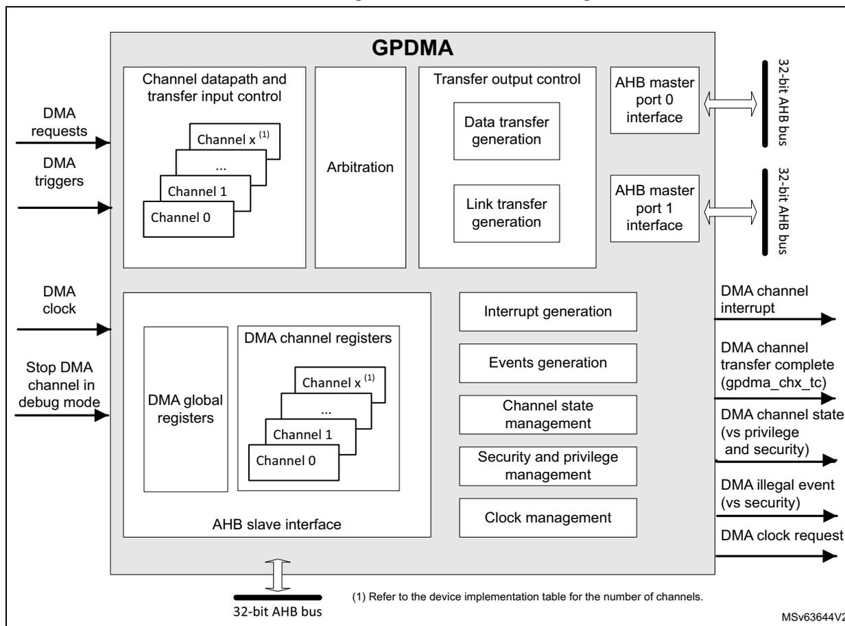
15.4.1 GPDMA block diagram
Figure 42. GPDMA block diagram
15.4.2 GPDMA channel state and direct programming without any linked-list
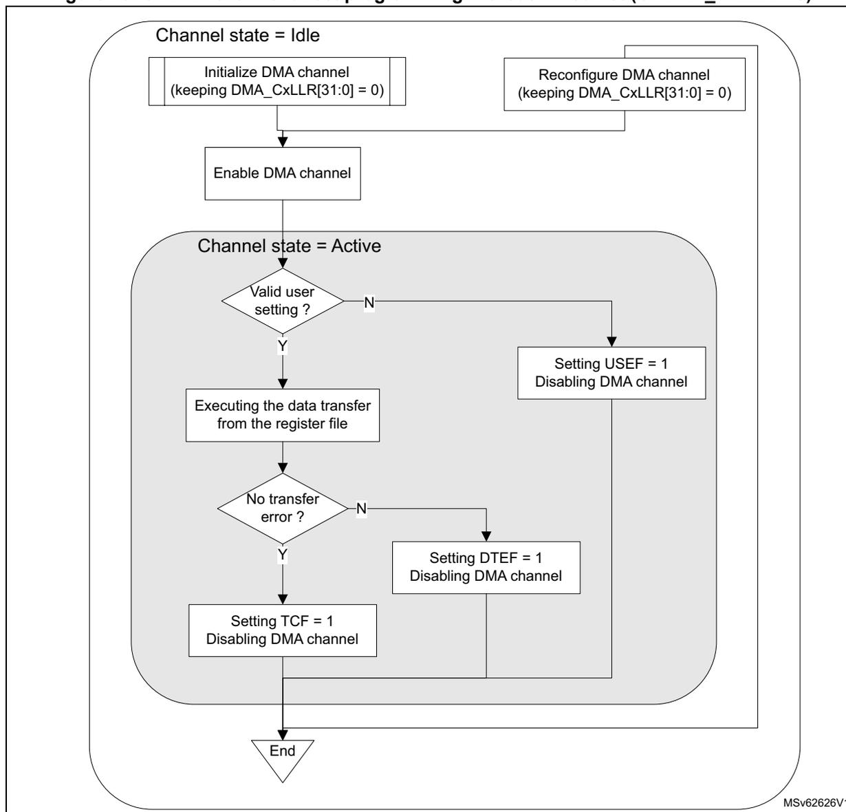
After a GPDMA reset, a GPDMA channel x is in idle state. When the software writes 1 in GPDMA_CxCR.EN, the channel takes into account the value of the different channel configuration registers (GPDMA_CxXXX), switches to the active/non-idle state and starts to execute the corresponding requested data transfers.
After enabling/starting a GPDMA channel transfer by writing 1 in GPDMA_CxCR.EN, a GPDMA channel interrupt on a complete transfer notifies the software that the GPDMA channel is back in idle state (EN is then deasserted by hardware) and that the channel is ready to be reconfigured then enabled again.
Figure 43 illustrates this GPDMA direct programming without any linked-list (GPDMA_CxLLR = 0).
Figure 43. GPDMA channel direct programming without linked-list (GPDMA_CxLLR = 0)
graph TD; subgraph Idle; A[Initialize DMA channel
(keeping DMA_CxLLR[31:0] = 0)]; B[Reconfigure DMA channel
(keeping DMA_CxLLR[31:0] = 0)]; end; A --> C[Enable DMA channel]; B --> C; C --> D{Valid user setting?}; subgraph Active; D -- N --> E[Setting USEF = 1
Disabling DMA channel]; D -- Y --> F[Executing the data transfer
from the register file]; F --> G{No transfer error?}; G -- N --> H[Setting DTEF = 1
Disabling DMA channel]; G -- Y --> I[Setting TCF = 1
Disabling DMA channel]; end; E --> J((End)); H --> J; I --> J;
The flowchart illustrates the direct programming of a GPDMA channel without a linked-list. It starts with the channel in an 'Idle' state, where it can be initialized or reconfigured (keeping DMA_CxLLR[31:0] = 0). The channel is then enabled. Once enabled, the channel enters an 'Active' state. In this state, the software checks if the user settings are valid. If not valid (N), the channel is disabled by setting USEF = 1. If valid (Y), the data transfer is executed from the register file. After the transfer, the software checks for a transfer error. If an error occurs (N), the channel is disabled by setting DTEF = 1. If no error occurs (Y), the channel is disabled by setting TCF = 1. Both disabling actions lead to the 'End' state.
MSv62626V1
15.4.3 GPDMA channel suspend and resume
The software can suspend on its own a channel still active, with the following sequence:
- 1. The software writes 1 into the GPDMA_CxCR.SUSP bit.
- 2. The software polls the suspended flag GPDMA_CxSR.SUSPF until SUSPF = 1, or waits for an interrupt previously enabled by writing 1 to GPDMA_CxCR.SUSPIE. Wait for the channel to be effectively in suspended state means wait for the completion of any ongoing GPDMA transfer over its master ports. Then the software can observe, in a steady state, any read register or register field that is hardware modifiable.
Note: An ongoing GPDMA transfer can be a data transfer (a source/destination burst transfer) or a link transfer for the internal update of the linked-list register file from the next linked-list item.
- 3. The software safely resumes the suspended channel by writing 0 to GPDMA_CxCR.SUSP.
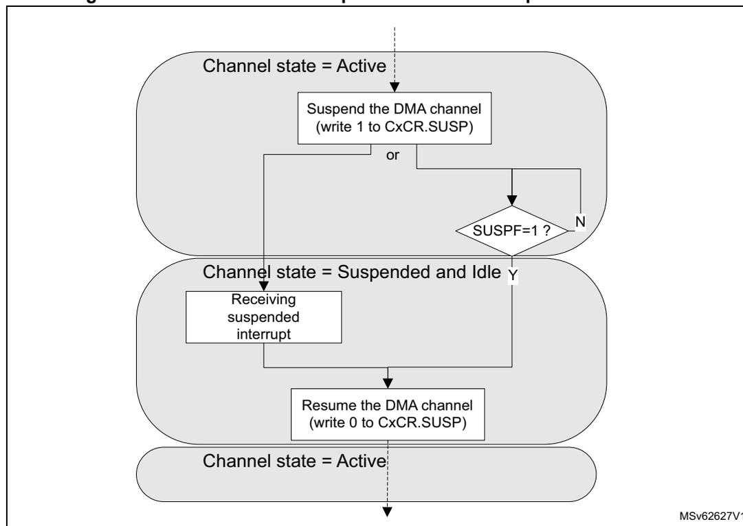
graph TD; A[Channel state = Active] --> B[Suspend the DMA channel<br/>(write 1 to CxCR.SUSP)]; A --> C[or]; B --> D{SUSPF=1?}; D -- N --> B; D -- Y --> E[Channel state = Suspended and Idle]; E --> F[Receiving suspended interrupt]; F --> G[Resume the DMA channel<br/>(write 0 to CxCR.SUSP)]; G --> H[Channel state = Active];MSv62627V1
Note: A suspend and resume sequence does not impact the GPDMA_CxCR.EN bit. Suspending a channel (transfer) does not suspend a started trigger detection.
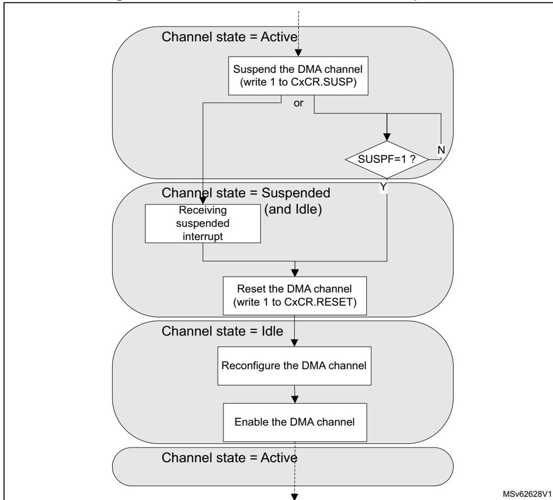
15.4.4 GPDMA channel abort and restart
Alternatively, like for aborting a continuous GPDMA transfer with a circular buffering or a double buffering, the software can abort, on its own, a still active channel with the following sequence:
- 1. The software writes 1 into the GPDMA_CxCR.SUSP bit.
- 2. The software polls suspended flag GPDMA_CxSR.SUSPF until SUSPF = 1, or waits for an interrupt previously enabled by writing 1 to GPDMA_CxCR.SUSPIE. Wait for the channel to be effectively in suspended state means wait for the completion of any ongoing GPDMA transfer over its master port.
- 3. The software resets the channel by writing 1 to GPDMA_CxCR.RESET. This causes the reset of the FIFO, the reset of the channel internal state, the reset of the GPDMA_CxCR.EN bit, and the reset of the GPDMA_CxCR.SUSP bit.
- 4. The software safely reconfigures the channel. The software must reprogram the hardware-modified GPDMA_CxBR1, GPDMA_CxSAR, and GPDMA_CxDAR registers.
- 5. In order to restart the aborted then reprogrammed channel, the software enables it again by writing 1 to the GPDMA_CxCR.EN bit.
Figure 45. GPDMA channel abort and restart sequence
graph TD
    Start(( )) -.-> Active1[Channel state = Active]
    subgraph Active1 [Channel state = Active]
        Suspend[Suspend the DMA channel
(write 1 to CxCR.SUSP)]
        SUSPF{SUSPF=1?}
        Suspend --> SUSPF
        SUSPF -- N --> SUSPF
    end
    SUSPF -- Y --> Suspended[Channel state = Suspended
(and Idle)]
    subgraph Suspended [Channel state = Suspended (and Idle)]
        Interrupt[Receiving suspended
interrupt]
        Reset[Reset the DMA channel
(write 1 to CxCR.RESET)]
        Interrupt --> Reset
    end
    Reset --> Idle[Channel state = Idle]
    subgraph Idle [Channel state = Idle]
        Reconfigure[Reconfigure the DMA channel]
        Enable[Enable the DMA channel]
        Reconfigure --> Enable
    end
    Enable --> Active2[Channel state = Active]
    Active2 -.-> End(( ))
The flowchart illustrates the sequence for aborting and restarting a GPDMA channel. It begins with the channel in an 'Active' state. The first step is to 'Suspend the DMA channel (write 1 to CxCR.SUSP)'. A loop exists within this state, checking if 'SUSPF=1?'. If 'No' (N), it loops back to the suspension step. If 'Yes' (Y), the channel transitions to a 'Suspended (and Idle)' state. In this state, the controller will be 'Receiving suspended interrupt' and then 'Reset the DMA channel (write 1 to CxCR.RESET)'. Following the reset, the channel enters an 'Idle' state, where it is 'Reconfigure the DMA channel' and then 'Enable the DMA channel'. Finally, the channel returns to an 'Active' state.
MSV62628V1
15.4.5 GPDMA linked-list data structure
Alternatively to the direct programming mode, a channel can be programmed by a list of transfers, known as a list of linked-list items (LLI). Each LLI is defined by its data structure.
The base address in memory of the data structure of a next \( LLI_{n+1} \) of a channel x is the sum of the following:
- • the link base address of the channel x (in GPDMA_CxLBAR)
- • the link address offset (LA[15:2] field in GPDMA_CxLLR). The linked-list register GPDMA_CxLLR is the updated result from the data structure of the previous \( LLI_n \) of the channel x.
The data structure for each LLI may be specific.
A linked-list data structure is addressed following the value of the following UT1, UT2, UB1, USA, UDA, UT3 and UB2 if present, and ULL bits in GPDMA_CxLLR.
In linked-list mode, each GPDMA linked-list register (GPDMA_CxTR1, GPDMA_CxTR2, GPDMA_CxBR1, GPDMA_CxSAR, GPDMA_CxDAR, GPDMA_CxTR3 and GPDMA_CxBR2 if present, and GPDMA_CxLLR) is conditionally and automatically updated from the next linked-list data structure in the memory, following the current value of the
GPDMA_CxLLR register that was conditionally updated from the linked-list data structure of the previous LLI.
Caution: The user must program the pointer to the next linked-list data structure (GPDMA_CxLLR[15:0]) not to exceed the 64-Kbyte addressable space defined by the link base address register (GPDMA_CxLBAR). The complete linked-list data structure must be included in the 64-Kbyte addressable space.
Static linked-list data structure
For example, when the update bits (UT1, UT2, UB1, USA, UDA, plus UB2 and UT3 if present, and ULL) in GPDMA_CxLLR are all asserted, the linked-list data structure in the memory is maximal with:
- • channel x (x = 0 to 9) contiguous 32-bit locations, including GPDMA_CxTR1, GPDMA_CxTR2, GPDMA_CxBR1, GPDMA_CxSAR, GPDMA_CxDAR and GPDMA_CxLLR (see Figure 46 ) and including the first linked-list register file (LLI 0 ) and the next LLIs (such as LLI 1 , LLI 2 ) in the memory
- • channel x (x = 10 to 11), contiguous 32-bit locations, including GPDMA_CxTR1, GPDMA_CxTR2, GPDMA_CxBR1, GPDMA_CxSAR, GPDMA_CxDAR, GPDMA_CxTR3, GPDMA_CxBR2 and GPDMA_CxLLR, (see Figure 47 ), and including the first linked-list register file (LLI 0 ) and the next LLIs (such as LLI 1 , LLI 2 ) in the memory
Figure 46. Static linked-list data structure (all Uxx = 1) of a linear addressing channel x
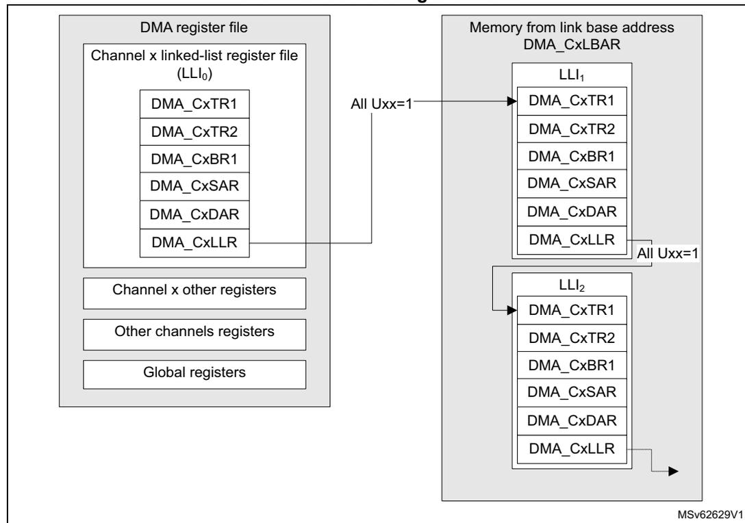
The diagram illustrates the static linked-list data structure for a linear addressing channel x. It is divided into two main sections: the DMA register file and the memory from the link base address DMA_CxLBAR.
DMA register file:
- Channel x linked-list register file (LLI 0 ) containing registers: DMA_CxTR1, DMA_CxTR2, DMA_CxBR1, DMA_CxSAR, DMA_CxDAR, and DMA_CxLLR.
- Channel x other registers
- Other channels registers
- Global registers
Memory from link base address DMA_CxLBAR:
- LLI 1 containing registers: DMA_CxTR1, DMA_CxTR2, DMA_CxBR1, DMA_CxSAR, DMA_CxDAR, and DMA_CxLLR. This LLI is pointed to by the DMA_CxLLR register in LLI 0 .
- LLI 2 containing registers: DMA_CxTR1, DMA_CxTR2, DMA_CxBR1, DMA_CxSAR, DMA_CxDAR, and DMA_CxLLR. This LLI is pointed to by the DMA_CxLLR register in LLI 1 .
The condition "All Uxx=1" is indicated for the registers in the memory LLIs (LLI 1 and LLI 2 ).
MSv62629V1
Figure 47. Static linked-list data structure (all Uxx = 1) of a 2D addressing channel x
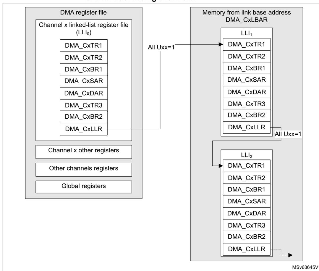
The diagram illustrates the static linked-list data structure for a 2D addressing channel x. On the left, the DMA register file is shown, containing the Channel x linked-list register file (LLI 0 ), Channel x other registers, Other channels registers, and Global registers. The LLI 0 contains the following registers: DMA_CxTR1, DMA_CxTR2, DMA_CxBR1, DMA_CxSAR, DMA_CxDAR, DMA_CxTR3, DMA_CxBR2, and DMA_CxLLR. On the right, the memory from link base address DMA_CxLBAR is shown, containing LLI 1 and LLI 2 . Both LLI 1 and LLI 2 contain the same set of registers: DMA_CxTR1, DMA_CxTR2, DMA_CxBR1, DMA_CxSAR, DMA_CxDAR, DMA_CxTR3, DMA_CxBR2, and DMA_CxLLR. An arrow labeled "All Uxx=1" points from the DMA_CxLLR in LLI 0 to the DMA_CxLLR in LLI 1 . Another arrow labeled "All Uxx=1" points from the DMA_CxLLR in LLI 1 to the DMA_CxLLR in LLI 2 . The diagram is labeled MSV63645V1.
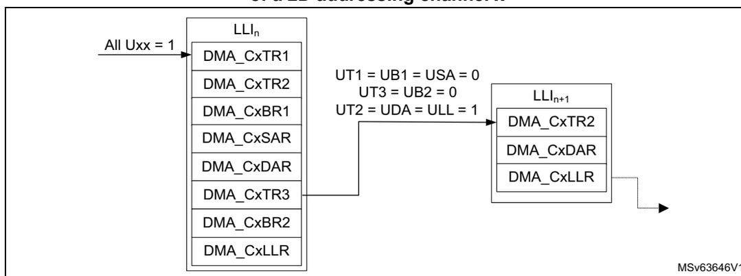
Dynamic linked-list data structure
Alternatively, the memory organization for the full list of LLIs can be compacted with specific data structure for each LLI.
If UT1 = 0 and UT2 = 1, the link address offset of the register GPDMA_CxLLR is pointing to the updated value of the GPDMA_CxTR2 instead of the GPDMA_CxTR1 which is not to be modified (see Figure 48 ).
Example: if UT1 = UB1 = USA = 0 and if UT3 = UB2 = 0, when channel x is with 2D addressing, and if UT2 = UDA = ULL = 1, the next LLI does not contain an (updated) value for GPDMA_CxTR1, nor GPDMA_CxBR1, nor GPDMA_CxSAR, nor GPDMA_CxTR3, nor GPDMA_CxBR2 when channel x is with 2D addressing. The next LLI contains an updated value for GPDMA_CxTR2, GPDMA_CxDAR, and GPDMA_CxLLR, as shown in Figure 49 .
Figure 48. GPDMA dynamic linked-list data structure of a linear addressing channel x
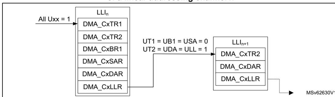
Figure 49. GPDMA dynamic linked-list data structure of a 2D addressing channel x
15.4.6 Linked-list item transfer execution
A \( LLI_n \) transfer is the sequence of:
- 1. a data transfer: GPDMA executes the data transfer as described by the GPDMA internal register file (this data transfer can be void/null for \( LLI_0 \) )
- 2. a conditional link transfer: GPDMA automatically and conditionally updates its internal register file by the data structure of the next \( LLI_{n+1} \) , as defined by the GPDMA_CxLLR value of the \( LLI_n \) .
Note: The initial data transfer as defined by the internal register file ( \( LLI_0 \) ) can be null (GPDMA_CxBR1.BNDT[15:0] = 0 and GPDMA_CxTR2.PFREQ = 0) provided that the conditional update bit UB1 in GPDMA_CxLLR is set (meaning there is a non-null data transfer described by the next \( LLI_1 \) in the memory to be executed).
Depending on the intended GPDMA usage, a GPDMA channel x can be executed as described by the full linked-list (run-to-completion mode, GPDMA_CxCR.LSM = 0) or a GPDMA channel x can be programmed for a single execution of a LLI (link step mode, GPDMA_CxCR.LSM = 1), as described in the next sections.
15.4.7 GPDMA channel state and linked-list programming in run-to-completion mode
When GPDMA_CxCR.LSM = 0 (in full list execution mode, execution of the full sequence of LLIs, named run-to-completion mode), a GPDMA channel x is initially programmed, started
by writing 1 to GPDMA_CxCR.EN, and after completed at channel level. The channel transfer is:
- • configured with at least the following:
- – the first \( LLI_0 \) , internal linked-list register file: GPDMA_CxTR1, GPDMA_CxTR2, GPDMA_CxBR1, GPDMA_CxSAR, GPDMA_CxDAR, and GPDMA_CxLLR, plus GPDMA_CxTR3 and GPDMA_CxBR2
- – the last \( LLI_N \) , described by the linked-list data structure in memory, as defined by the GPDMA_CxLLR reflecting the before last \( LLI_{N-1} \)
- • completed when GPDMA_CxLLR[31:0] = 0, GPDMA_CxBR1.BRC[10:0] = 0, and GPDMA_CxBR1.BNDT[15:0] = 0, at the end of the last \( LLI_{N-1} \) transfer
GPDMA_CxLLR[31:0] = 0 is the condition of a linked-list based channel completion and means the following:
- • The 16 low significant bits GPDMA_CxLLR.LA[15:0] of the next link address are null.
- • All the update bits GPDMA_CxLLR.Uxx are null (UT1, UT2, UB1, USA, UDA and ULL, plus UB2 and UT3).
The channel may never be completed when GPDMA_CxLLR.LSM = 0:
- • If the last
\(
LLI_N
\)
is recursive, pointing to itself as a next LLI:
- – either GPDMA_CxLLR.ULL = 1 and GPDMA_CxLLR.LA[15:2] is updated with the same value
- – or GPDMA_CxLLR.ULL = 0
- • If \( LLI_N \) is pointing to a previous LLI
In the regular data transfer completion at a block level, GPDMA_CxBR1.BNDT[15:0] = 0 and GPDMA_CxBR1.BRC[10:0] = 0 (if present). Alternatively, a block transfer may be early completed by a peripheral (such as an I3C in Rx mode), and then BNDT[15:0] is not null (see Section 15.4.14 for more details).
In the typical run-to-completion mode, the allocation of a GPDMA channel, including its fine programming, is done once during the GPDMA initialization. In order to have a reserved data communication link and GPDMA service during run-time, for continuously repeated transfers (from/to a peripheral respectively to/from memory or for memory-to-memory transfers). This reserved data communication link can consist of a channel, or the channel can be shared and a repeated transfer consists of a sequence of LLIs.
Figure 50 depicts the GPDMA channel execution and its registers programming in run-to-completion mode.
Note: Figure 50 is not intended to illustrate how often a TCEF can be raised, depending on the programmed value of TCEM[1:0] in GPDMA_CxTR2. It can be raised at (each) block completion, at (each) 2D block completion, at (each) LLI completion, or only at channel completion. In run-to-completion mode, whatever is the value of TCEM[1:0], at the channel completion, the hardware always set TCEF = 1 and disables the channel.
In Figure 50 , BNDT ≠ 0 is the typical condition for starting the first data transfer in this figure. This condition becomes (BNDT ≠ 0 and PFREQ = 1) if the peripheral requests a data transfer with early termination (see Section 15.3.5 ).
Figure 50. GPDMA channel execution and linked-list programming in run-to-completion mode (GPDMA_CxCR.LSM = 0)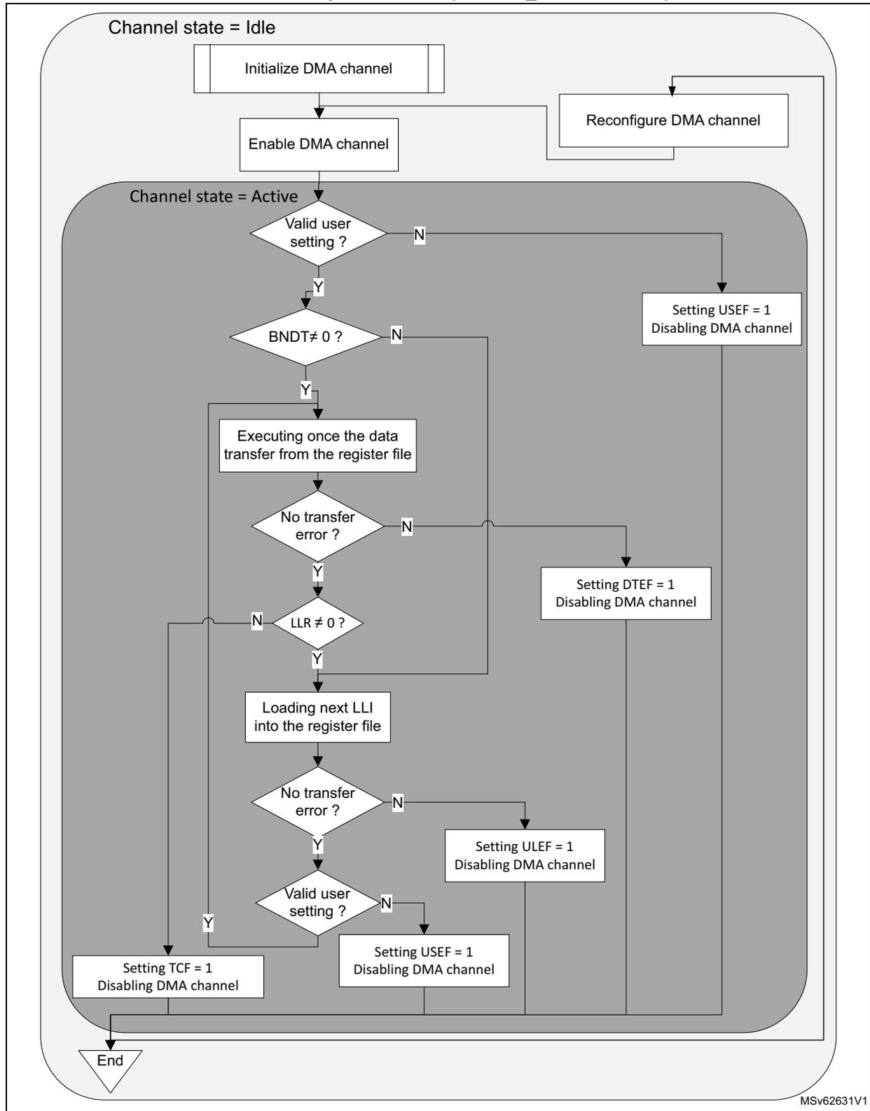
graph TD; subgraph Idle; A[Initialize DMA channel] --> B[Enable DMA channel]; B --> C{Valid user setting?}; C -- N --> D[Setting USEF = 1
Disabling DMA channel]; D --> E[Reconfigure DMA channel]; E --> C; C -- Y --> F{BNDT ≠ 0?}; F -- N --> G[Setting DTEF = 1
Disabling DMA channel]; F -- Y --> H[Executing once the data transfer from the register file]; H --> I{No transfer error?}; I -- N --> G; I -- Y --> J{LLR ≠ 0?}; J -- N --> K[Setting TCF = 1
Disabling DMA channel]; J -- Y --> L[Loading next LLI into the register file]; L --> M{No transfer error?}; M -- N --> G; M -- Y --> N1{Valid user setting?}; N1 -- N --> O[Setting USEF = 1
Disabling DMA channel]; N1 -- Y --> K; K --> P[End]; O --> P; G --> P; E --> P;
The flowchart illustrates the execution and linked-list programming of a GPDMA channel in run-to-completion mode. It is divided into two main states: Channel state = Idle and Channel state = Active .
Channel state = Idle :
- The process starts with Initialize DMA channel , followed by Enable DMA channel .
- A decision Valid user setting? is made. If N (No), the channel is disabled by Setting USEF = 1 and then Reconfigure DMA channel occurs, returning to the Valid user setting? decision.
- If Y (Yes), the channel enters the Channel state = Active .
Channel state = Active :
- A decision Valid user setting? is made. If N , the channel is disabled by Setting USEF = 1 .
- If Y , a decision BNDT ≠ 0? is made. If N , the channel is disabled by Setting DTEF = 1 .
- If Y , the channel executes Executing once the data transfer from the register file .
- A decision No transfer error? is made. If N , the channel is disabled by Setting DTEF = 1 .
- If Y , a decision LLR ≠ 0? is made. If N , the channel is disabled by Setting TCF = 1 .
- If Y , the channel executes Loading next LLI into the register file .
- A decision No transfer error? is made. If N , the channel is disabled by Setting DTEF = 1 .
- If Y , a decision Valid user setting? is made. If N , the channel is disabled by Setting USEF = 1 .
- If Y , the channel is disabled by Setting TCF = 1 .
All disabling actions ( Setting USEF = 1 , Setting DTEF = 1 , Setting TCF = 1 ) lead to the End state. The End state also leads back to the Reconfigure DMA channel step in the Idle state.
MSv62631V1
Run-time inserting a \( LLI_n \) via an auxiliary channel, in run-to-completion modeThe start of the link transfer of the \( LLI_{n-1} \) (start of the \( LLI_n \) loading) can be conditioned by the occurrence of a trigger, when programming the following fields of the GPDMA_CxTR2 in the data structure of the \( LLI_{n-1} \) :
- • TRIGM[1:0] = 10 (link transfer triggering mode)
- • TRIGPOL[1:0] = 01 or 10 (rising or falling edge)
- • TRIGSEL[5:0] (see Section 15.3.6 for the trigger selection details)
Another auxiliary channel y can be used to store the channel x \( LLI_n \) in the memory and to generate a transfer complete event gpdma_chy_tc. By selecting this event as the input trigger of the link transfer of the \( LLI_{n-1} \) of the channel x, the software can pause the primary channel x after its \( LLI_{n-1} \) data transfer, until it is indeed written the \( LLI_n \) .
Figure 51 depicts such a dynamic elaboration of a linked-list of a primary channel x, via another auxiliary channel y.
Caution: This use case is restricted to an application with a \( LLI_{n-1} \) data transfer that does not need a trigger. The triggering mode of this \( LLI_{n-1} \) is used to load the next \( LLI_n \) .
Figure 51. Inserting a LLI n with an auxiliary GPDMA channel y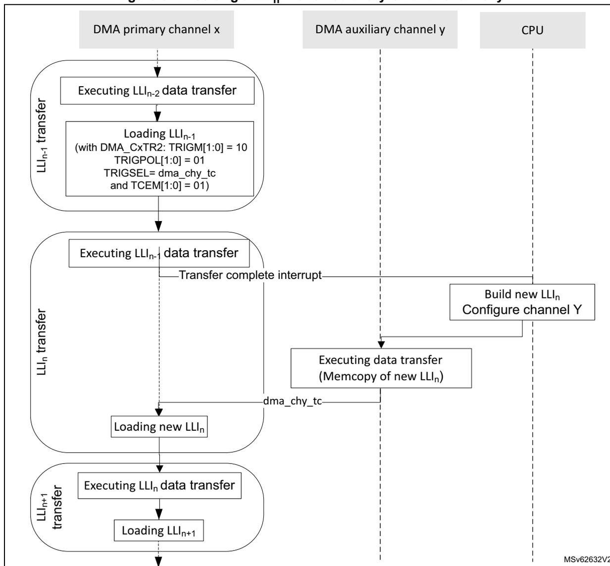
sequenceDiagram
    participant DMA_x as DMA primary channel x
    participant DMA_y as DMA auxiliary channel y
    participant CPU as CPU

    Note left of DMA_x: LLI_{n-2} transfer
    DMA_x->>DMA_x: Executing LLI_{n-2} data transfer
    DMA_x->>DMA_x: Loading LLI_{n-1} (with DMA_CxTR2: TRIGM[1:0] = 10, TRIGPOL[1:0] = 01, TRIGSEL=dma_chy_tc and TCEM[1:0] = 01)

    Note left of DMA_x: LLI_{n-1} transfer
    DMA_x->>DMA_x: Executing LLI_{n-1} data transfer
    DMA_x-->>CPU: Transfer complete interrupt

    Note right of CPU: Build new LLI_n, Configure channel Y
    CPU-->>DMA_y:
    DMA_y->>DMA_y: Executing data transfer (Memcopy of new LLI_n)
    DMA_y-->>DMA_x: dma_chy_tc

    Note left of DMA_x: LLI_n transfer
    DMA_x->>DMA_x: Loading new LLI_n
    DMA_x->>DMA_x: Executing LLI_n data transfer

    Note left of DMA_x: LLI_{n+1} transfer
    DMA_x->>DMA_x: Loading LLI_{n+1}
15.4.8 GPDMA channel state and linked-list programming in link step mode
When GPDMA_CxCR.LSM = 1 (in link step execution mode, single execution of one LLI), a channel transfer is executed and completed after each single execution of a LLI, including its (conditional) data transfer and its (conditional) link transfer.
A GPDMA channel transfer can be programmed at LLI level, started by writing 1 into GPDMA_CxCR.EN, and after completed at LLI level:
- • The current LLI
n
transfer is described with:
- – GPDMA_CxTR1 defines the source/destination elementary single/burst transfers.
- – GPDMA_CxBR1 defines the number of bytes at a block level (BNDT[15:0]) and, for channel x (x = 10 to 11), the number of blocks at a 2D/repeated block level (BRC[10:0]+1) and the incrementing/decrementing mode for address offsets.
- – GPDMA_CxTR2 defines the input control (request, trigger) and the output control (transfer complete event) of the transfer.
- – GPDMA_CxSAR/GPDMA_CxDAR define the source/destination transfer start address.
- – GPDMA_CxTR3 for channel x (x = 10 to 11) defines the source/destination additional address offset between burst transfers.
- – GPDMA_CxBR2 for channel x (x = 10 to 11) defines the source/destination additional address offset between blocks at a 2D/repeated block level.
- – GPDMA_CxLLR defines the data structure and the address offset of the next \( LLI_{n+1} \) in the memory.
- • The current
\(
LLI_n
\)
transfer is completed after the single execution of the current
\(
LLI_n
\)
:
- – after the (conditional) data transfer completion (when \( GPDMA\_CxBR1.BRC[10:0] = 0 \) , and \( GPDMA\_CxBR1.BNDT[15:0] = 0 \) )
- – after the (conditional) update of the GPDMA link register file from the data structure of the next \( LLI_{n+1} \) in memory
Note: If a LLI is recursive (pointing to itself as a next LLI, either \( GPDMA\_CxLLR.ULL = 1 \) and \( GPDMA\_CxLLR.LA[15:2] \) is updated with the same value, or \( GPDMA\_CxLLR.ULL = 0 \) ), a channel in link step mode is completed after each repeated single execution of this LLI.
In the regular data transfer completion at a block level, \( GPDMA\_CxBR1.BNDT[15:0] = 0 \) and \( GPDMA\_CxBR1.BRC[10:0] = 0 \) . Alternatively, a block transfer may be early completed by a peripheral (such as an I3C in Rx mode), and then \( BNDT[15:0] \) is not null (see Section 15.4.14 for more details).
The link step mode can be used to elaborate dynamically LLIs in memory during run-time. The software can be facilitated by using a static data structure for any \( LLI_n \) (all update bits of \( GPDMA\_CxLLR \) have a static value, \( LLI_n.LLR.LA = LLI_{n-1}.LLR.LA + \text{constant} \) ).
Figure 52 depicts the GPDMA channel execution mode, and its programming in link step mode.
Note: Figure 52 is not intended to illustrate how often a TCEF can be raised, depending on the programmed value of \( TCEM[1:0] \) in \( GPDMA\_CxTR2 \) . It can be raised at (each) block completion, at (each) 2D block completion, at (each) LLI completion, or only at the last LLI data transfer completion. In link step mode, the channel is disabled after each single execution of a LLI, and depending on the value of \( TCEM[1:0] \) a TCEF is raised or not. In Figure 52 , \( BNDT \neq 0 \) is the typical condition for starting the first data transfer. This condition becomes ( \( BNDT \neq 0 \) and \( PFREQ = 1 \) ) if the peripheral requests a data transfer with early termination (see Section 15.3.5 ).
Figure 52. GPDMA channel execution and linked-list programming in link step mode (GPDMA_CxCR.LSM = 1)

graph TD; subgraph Idle; A[Initialize DMA channel] --> B[Enable DMA channel]; end; B --> subgraph Active; C{Valid user setting?}; D{BNDT != 0?}; E[Executing once the data transfer from the register file]; F{No transfer error?}; G{LLR != 0?}; H[Loading next LLI into the register file]; I{No transfer error?}; J{Valid user setting?}; K[Setting TCF = 1 Disabling DMA channel]; L[Setting USEF = 1 Disabling DMA channel]; M[Setting DTEF = 1 Disabling DMA channel]; N[Setting ULEF = 1 Disabling DMA channel]; O[End]; A --> B; B --> C; C -- Y --> D; C -- N --> L; D -- Y --> E; D -- N --> M; E --> F; F -- Y --> G; F -- N --> M; G -- Y --> H; G -- N --> K; H --> I; I -- Y --> J; I -- N --> N; J -- Y --> K; J -- N --> L; K --> O; L --> O; M --> O; N --> O; O --> P[Reconfigure DMA channel]; P --> B;MSv62633V1
Run-time adding a \( LLI_{n+1} \) in link step mode
During run-time, the software can defer the elaboration of the \( LLI_{n+1} \) (and next LLIs), until/after GPDMA executed the transfer from the \( LLI_{n-1} \) and loaded the \( LLI_n \) from the memory, as shown in Figure 53.
Figure 53. Building \( LLI_{n+1} \) : GPDMA dynamic linked-lists in link step mode
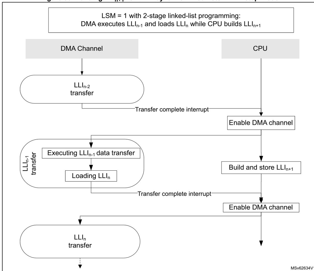
LSM = 1 with 2-stage linked-list programming:
DMA executes
\(
LLI_{n-1}
\)
and loads
\(
LLI_n
\)
while CPU builds
\(
LLI_{n+1}
\)
sequenceDiagram
    participant DMA Channel
    participant CPU
    Note right of DMA Channel: LSM = 1 with 2-stage linked-list programming: DMA executes LLI_{n-1} and loads LLI_n while CPU builds LLI_{n+1}
    DMA Channel->>DMA Channel: LLI_{n-2} transfer
    DMA Channel->>CPU: Transfer complete interrupt
    CPU->>DMA Channel: Enable DMA channel
    DMA Channel->>DMA Channel: LLI_{n-1} transfer (Executing LLI_{n-1} data transfer, Loading LLI_n)
    DMA Channel->>CPU: Transfer complete interrupt
    CPU->>CPU: Build and store LLI_{n+1}
    CPU->>DMA Channel: Enable DMA channel
    DMA Channel->>DMA Channel: LLI_n transfer
MSv62634V1
Run-time replacing a \( LLI_n \) with a new \( LLI_{n'} \) in link step mode (in linked-list register file)
In this link step mode, during run-time, the software can build and insert a new \( LLI_{n'} \) , after GPDMA executed the transfer from the \( LLI_{n-1} \) and loaded a formerly elaborated \( LLI_n \) from the memory by overwriting directly the linked-list register file with the new \( LLI_{n'} \) , as shown in Figure 54.
Figure 54. Replace with a new \( LLI_{n'} \) in register file in link step mode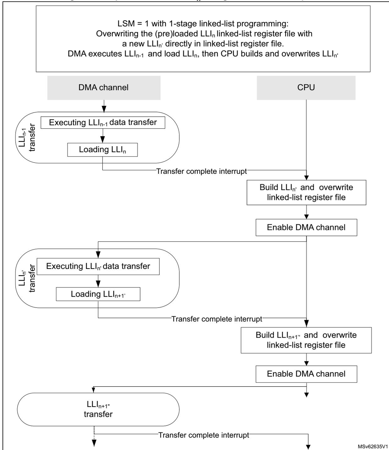
LSM = 1 with 1-stage linked-list programming:
Overwriting the (pre)loaded
\(
LLI_n
\)
linked-list register file with
a new
\(
LLI_{n'}
\)
directly in linked-list register file.
DMA executes
\(
LLI_{n-1}
\)
and load
\(
LLI_n
\)
, then CPU builds and overwrites
\(
LLI_{n'}
\)
  sequenceDiagram
      participant DMA as DMA channel
      participant CPU as CPU

      Note over DMA: LLI_{n-1} transfer
      DMA->>DMA: Executing LLI_{n-1} data transfer
      DMA->>DMA: Loading LLI_n
      DMA->>CPU: Transfer complete interrupt

      Note over CPU: Build LLI_{n'} and overwrite linked-list register file
      Note over CPU: Enable DMA channel

      Note over DMA: LLI_{n'} transfer
      DMA->>DMA: Executing LLI_{n'} data transfer
      DMA->>DMA: Loading LLI_{n+1''}
      DMA->>CPU: Transfer complete interrupt

      Note over CPU: Build LLI_{n+1''} and overwrite linked-list register file
      Note over CPU: Enable DMA channel

      Note over DMA: LLI_{n+1''} transfer
      DMA->>DMA: LLI_{n+1''} transfer
      DMA->>CPU: Transfer complete interrupt
MSV62635V1
The software can build and insert a new \( LLI_{n'} \) and \( LLI_{n+1''} \) in the memory, after GPDMA executed the transfer from the \( LLI_{n-1} \) and loaded a formerly elaborated \( LLI_n \) from the memory, by overwriting partly the linked-list register file (GPDMA_CxBR1.BNDT[15:0] to be null and GPDMA_CxLLR to point to new \( LLI_{n'} \) ) as shown in Figure 55 .
Figure 55. Replace with a new\( LLI_{n'} \) and \( LLI_{n+1'} \) in memory in link step mode (option 1)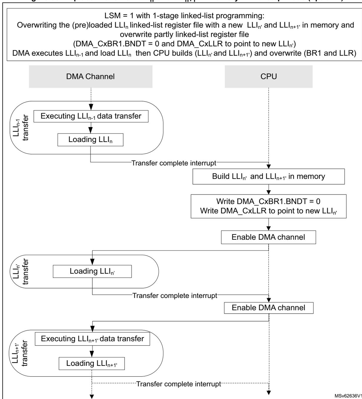
LSM = 1 with 1-stage linked-list programming:
Overwriting the (pre)loaded
\(
LLI_n
\)
linked-list register file with a new
\(
LLI_{n'}
\)
and
\(
LLI_{n+1'}
\)
in memory and overwrite partly linked-list register file
(DMA_CxBR1.BNDT = 0 and DMA_CxLLR to point to new
\(
LLI_{n'}
\)
)
DMA executes
\(
LLI_{n-1}
\)
and load
\(
LLI_n
\)
then CPU builds (
\(
LLI_{n'}
\)
and
\(
LLI_{n+1'}
\)
) and overwrite (BR1 and LLR)
sequenceDiagram
    participant DMA Channel
    participant CPU

    Note right of DMA Channel: LSM = 1 with 1-stage linked-list programming: Overwriting the (pre)loaded LLI_n linked-list register file with a new LLI_n' and LLI_{n+1'} in memory and overwrite partly linked-list register file (DMA_CxBR1.BNDT = 0 and DMA_CxLLR to point to new LLI_n') DMA executes LLI_{n-1} and load LLI_n then CPU builds (LLI_n' and LLI_{n+1'}) and overwrite (BR1 and LLR)

    Note left of DMA Channel: LLI_{n-1} transfer
    DMA Channel->>DMA Channel: Executing LLI_{n-1} data transfer
    DMA Channel->>DMA Channel: Loading LLI_n
    DMA Channel->>CPU: Transfer complete interrupt
    Note right of CPU: Build LLI_n' and LLI_{n+1'} in memory
    Note right of CPU: Write DMA_CxBR1.BNDT = 0
    Note right of CPU: Write DMA_CxLLR to point to new LLI_n'
    Note right of CPU: Enable DMA channel
    Note left of DMA Channel: LLI_{n'} transfer
    DMA Channel->>DMA Channel: Loading LLI_{n'}
    DMA Channel->>CPU: Transfer complete interrupt
    Note right of CPU: Enable DMA channel
    Note left of DMA Channel: LLI_{n+1'} transfer
    DMA Channel->>DMA Channel: Executing LLI_{n+1'} data transfer
    DMA Channel->>DMA Channel: Loading LLI_{n+1'}
    DMA Channel-->>CPU: Transfer complete interrupt
The diagram illustrates the sequence of operations for replacing linked-list items in memory. It starts with the DMA Channel executing the \( LLI_{n-1} \) data transfer and loading \( LLI_n \) . Upon completion, a transfer complete interrupt is sent to the CPU. The CPU then builds the new \( LLI_{n'} \) and \( LLI_{n+1'} \) in memory, writes \( DMA\_CxBR1.BNDT = 0 \) and updates \( DMA\_CxLLR \) to point to the new \( LLI_{n'} \) , and enables the DMA channel. The DMA Channel then loads \( LLI_{n'} \) . Upon completion, another transfer complete interrupt is sent to the CPU, which enables the DMA channel again. Finally, the DMA Channel executes the \( LLI_{n+1'} \) data transfer and loads \( LLI_{n+1'} \) , sending a final transfer complete interrupt to the CPU.
MSV62636V1
Run-time replacing a \( LLI_n \) with a new \( LLI_{n'} \) in link step mode
Other software implementations exist. Meanwhile GPDMA executes the transfer from the \( LLI_{n-1} \) and loads a formerly elaborated \( LLI_n \) from the memory (or even earlier), the software can do the following:
- 1. Disable the NVIC for not being interrupted by the interrupt handling.
- 2. Build a new \( LLI_{n'} \) and a new \( LLI_{n+1'} \) .
- 3. Enable again the NVIC for the channel interrupt (transfer complete) notification.
The software in the interrupt handler for \( LLI_{n-1} \) is then restricted to overwrite GPDMA_CxBR1.BNDT[15:0] to be null and GPDMA_CxLLR to point to new \( LLI_{n'} \) , as shown in Figure 56 .
Figure 56. Replace with a new \( LLI_{n'} \) and \( LLI_{n+1'} \) in memory in link step mode (option 2)
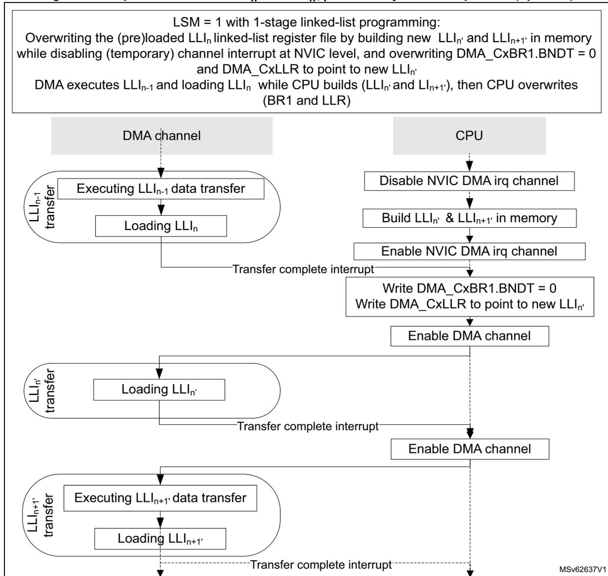
LSM = 1 with 1-stage linked-list programming:
Overwriting the (pre)loaded
\(
LLI_n
\)
linked-list register file by building new
\(
LLI_{n'}
\)
and
\(
LLI_{n+1'}
\)
in memory while disabling (temporary) channel interrupt at NVIC level, and overwriting DMA_CxBR1.BNDT = 0 and DMA_CxLLR to point to new
\(
LLI_{n'}
\)
DMA executes
\(
LLI_{n-1}
\)
and loading
\(
LLI_n
\)
while CPU builds (
\(
LLI_{n'}
\)
and
\(
LLI_{n+1'}
\)
), then CPU overwrites (BR1 and LLR)
sequenceDiagram
    participant DMA as DMA channel
    participant CPU as CPU

    Note over DMA: LLI_{n-1} transfer
    DMA->>DMA: Executing LLI_{n-1} data transfer
    DMA->>DMA: Loading LLI_n
    DMA-->>CPU: Transfer complete interrupt

    CPU->>CPU: Disable NVIC DMA irq channel
    CPU->>CPU: Build LLI_{n'} & LLI_{n+1'} in memory
    CPU->>CPU: Enable NVIC DMA irq channel
    CPU->>CPU: Write DMA_CxBR1.BNDT = 0
    CPU->>CPU: Write DMA_CxLLR to point to new LLI_{n'}
    CPU->>CPU: Enable DMA channel

    Note over DMA: LLI_{n'} transfer
    DMA->>DMA: Loading LLI_{n'}
    DMA-->>CPU: Transfer complete interrupt
    CPU->>CPU: Enable DMA channel

    Note over DMA: LLI_{n+1'} transfer
    DMA->>DMA: Executing LLI_{n+1'} data transfer
    DMA->>DMA: Loading LLI_{n+1'}
    DMA-->>CPU: Transfer complete interrupt
MSv62637V1
15.4.9 GPDMA channel state and linked-list programming
The software can reconfigure a channel when the channel is disabled (GPDMA_CxCR.EN = 0) and update the execution mode (GPDMA_CxCR.LSM) to change from/to run-to-completion mode to/from link step mode.
In any execution mode, the software can:
- • reprogram \( LLI_{n+1} \) in the memory to finally complete the channel by this \( LLI_{n+1} \) (clear the GPDMA_CxLLR of this \( LLI_{n+1} \) ), before this \( LLI_{n+1} \) is loaded/used by the GPDMA channel
- • abort and reconfigure the channel with a LSM update (see Section 15.4.4. )
In link step mode, the software can clear LSM after each a single execution of any LLI, during \( LLI_{n-1} \) .
Figure 57 shows the overall and unified GPDMA linked-list programming, whatever is the execution mode.
Note: Figure 57 is not intended to illustrate how often a TCEF can be raised, depending on the programmed value of TCEM[1:0] in GPDMA_CxTR2. It can be raised at (each) block completion, at (each) 2D block completion, at (each) LLI completion, or only at the last LLI data transfer completion. In run-to-completion mode, whatever is the value of TCEM[1:0], at the channel completion the hardware always set TCEF = 1 and disables the channel. In link step mode, the channel is disabled after each single execution of a LLI, and depending on the value of TCEM[1:0] a TCEF is raised or not.
In Figure 57 , BNDT \( \neq \) 0 is the typical condition for starting the first data transfer. This condition becomes (BNDT \( \neq \) 0 and PFREQ = 1) if the peripheral requests a data transfer with early termination (see Section 15.3.5 ).
Figure 57. GPDMA channel execution and linked-list programming
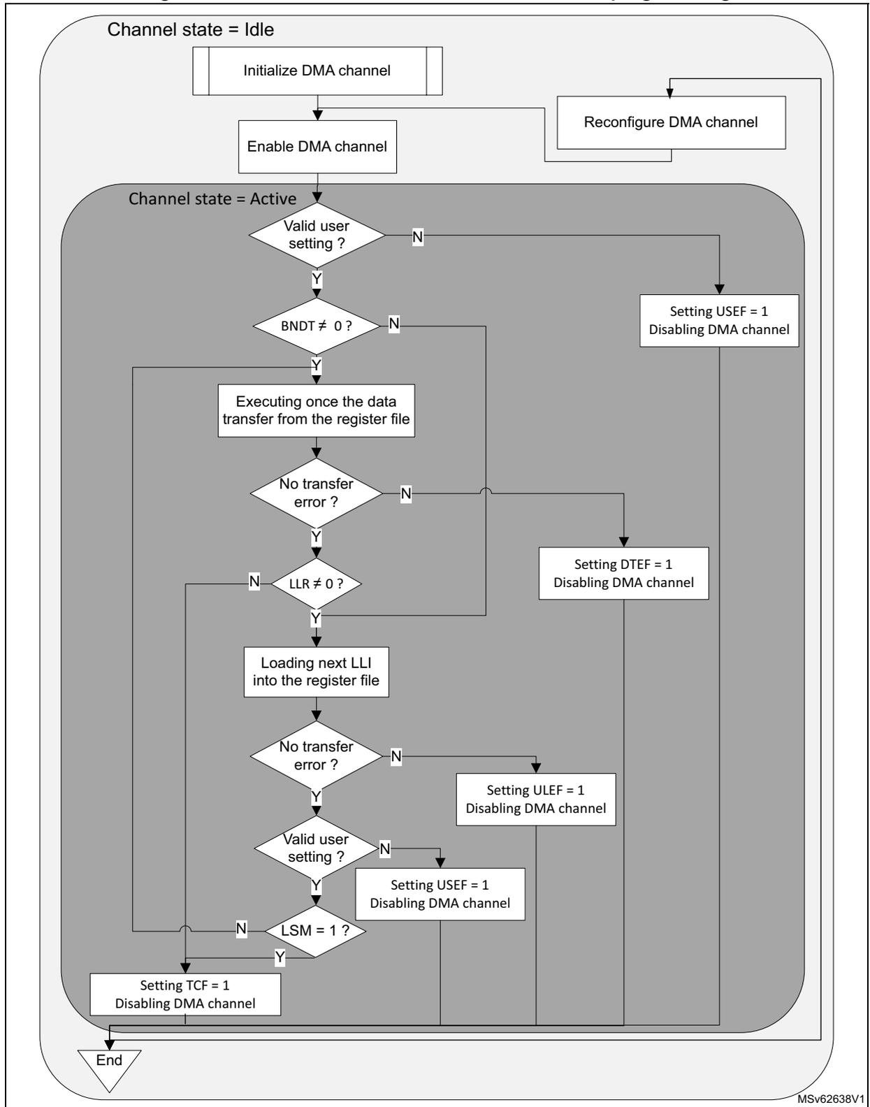
graph TD; subgraph Idle [Channel state = Idle]; Init[Initialize DMA channel] --> Enable[Enable DMA channel]; End([End]) --> Init; end; Enable --> Active [Channel state = Active]; subgraph Active; Valid1{Valid user setting?}; BNDT{BNDT != 0?}; Exec[Executing once the data transfer from the register file]; NoError1{No transfer error?}; LLR{LLR != 0?}; LoadLLI[Loading next LLI into the register file]; NoError2{No transfer error?}; Valid2{Valid user setting?}; LSM{LSM = 1?}; TCF[Setting TCF = 1 Disabling DMA channel]; USEF1[Setting USEF = 1 Disabling DMA channel]; DTEF[Setting DTEF = 1 Disabling DMA channel]; ULEF[Setting ULEF = 1 Disabling DMA channel]; USEF2[Setting USEF = 1 Disabling DMA channel]; Valid1 -- Y --> BNDT; BNDT -- Y --> Exec; Exec --> NoError1; NoError1 -- N --> USEF1; NoError1 -- Y --> LLR; LLR -- Y --> LoadLLI; LoadLLI --> NoError2; NoError2 -- N --> ULEF; NoError2 -- Y --> Valid2; Valid2 -- N --> USEF2; Valid2 -- Y --> LSM; LSM -- Y --> TCF; LSM -- N --> Valid1; TCF --> End; USEF1 --> End; DTEF --> End; ULEF --> End; USEF2 --> End; end;MSv62638V1
15.4.10 GPDMA FIFO-based transfers
There is a single transfer operation mode: the FIFO mode. There are FIFO-based transfers. Any channel x is implemented with a dedicated FIFO whose size is defined by
dma_fifo_size[x]
(see
Section 15.3.1
for more details).
GPDMA burst
A programmed transfer at the lowest level is a GPDMA burst.
A GPDMA burst is a burst of data received from the source, or a burst of data sent to the destination. A source (and destination) burst is programmed with a burst length by the field
SBL_1[5:0]
(respectively
DBL_1[5:0]
), and with a data width defined by the field
SDW_LOG2[1:0]
(respectively
DDW_LOG2[1:0]
) in the
GPDMA_CxTR1
register.
The addressing mode after each data (named beat) of a GPDMA burst is defined by
SINC
and
DINC
in
GPDMA_CxTR1
, for source and destination respectively: either a fixed addressing or an incremented addressing with contiguous data.
The start and next addresses of a GPDMA source/destination burst (defined by
GPDMA_CxSAR
and
GPDMA_CxDAR
) must be aligned with the respective data width.
The table below lists the main characteristics of a GPDMA burst.
Table 129. Programmed GPDMA source/destination burst
| SDW_LOG2[1:0] DDW_LOG2[1:0] | Data width (bytes) | SINC/DINC | SBL_1[5:0] DBL_1[5:0] | Burst length (data/beats) | Next data/beat address | Next burst address | Burst address alignment |
|---|---|---|---|---|---|---|---|
| 00 | 1 | 0 (fixed) | n = 0 to 63 (1) | n+1 | + 0 | + 0 | 1 |
| 01 | 2 | 2 | |||||
| 10 | 4 | 4 | |||||
| 00 | 1 | 1 (contiguously incremented) | + 1 | + (n + 1) | 1 | ||
| 01 | 2 | + 2 | + 2 * (n + 1) | 2 | |||
| 10 | 4 | + 4 | + 4 * (n + 1) | 4 | |||
| 11 | forbidden user setting, causing USEF generation and none burst to be issued. | ||||||
- 1. When S/DBL_1[5:0] = 0, burst is of length 1. Then burst can be also named as single.
The next burst address in the above table is the next source/destination default address pointed by
GPDMA_CxSAR
or
GPDMA_CxDAR
, once the programmed source/destination burst is completed. This default value refers to the fixed/contiguously incremented address.
When the channel has additional 2D addressing feature, this default value refers to the value without taking into account the two programmed incremented or decremented offsets. These two additional offsets (with a null default value) are applied:
- • after each completed source/destination burst, as defined respectively by GPDMA_CxTR2.SAO[12:0]/DAO[12:0] and GPDMA_CxBR1.SDEC/DDEC
- • after each completed block, as defined respectively by GPDMA_CxBR2.BRSAO[15:0]/BRDAO[15:0] and GPDMA_CxBR1.BRSDEC/BRDDEC)
Then, a 2D/repeated block can be addressed with a first programmed address jump after each completed burst, and with a second programmed address jump after each block, as depicted by Figure 58 with a 2D destination buffer.
Figure 58. Programmed 2D addressing
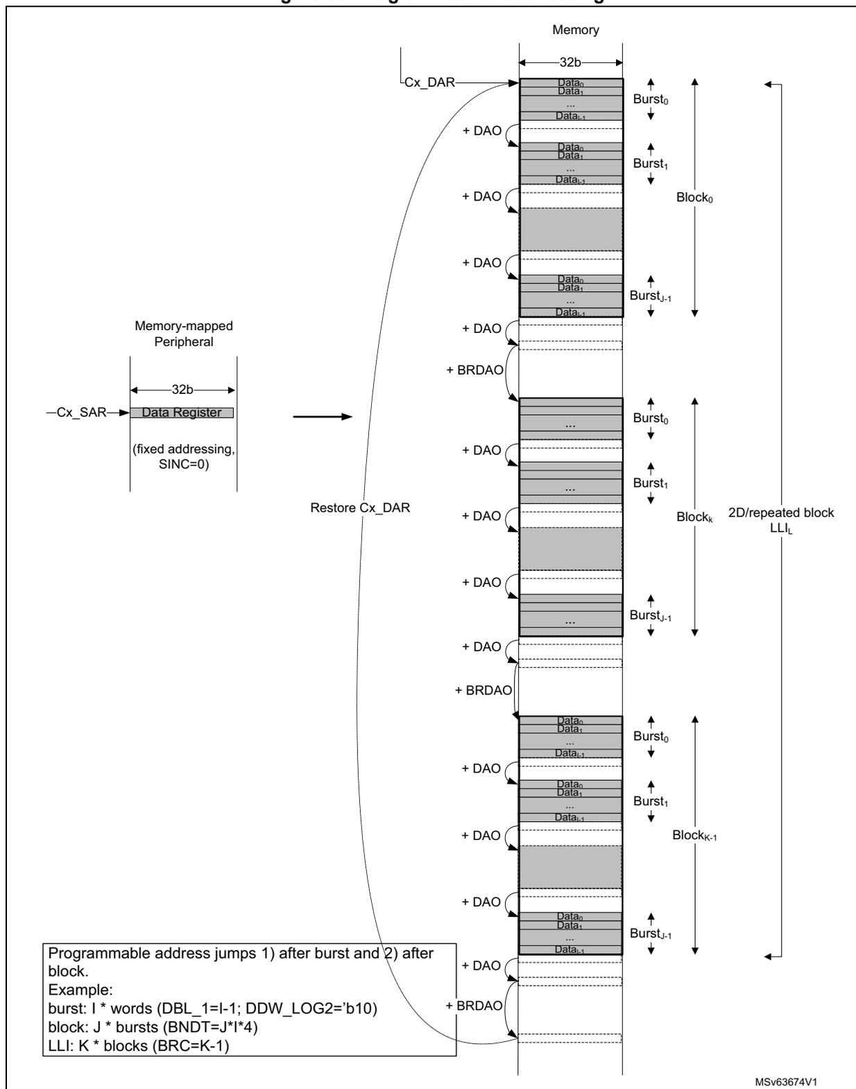
The diagram illustrates the memory addressing scheme for a 2D DMA transfer. On the left, a 'Memory-mapped Peripheral' contains a 'Data Register' (32b wide) with 'fixed addressing, SINC=0'. The source address is 'Cx_SAR'. An arrow points from the Data Register to the 'Memory' on the right. The 'Memory' is organized into 'Bursts' and 'Blocks'. Each 'Burst' contains 'Data n ' and 'Data n-1 ' (32b wide). The 'Bursts' are grouped into 'Blocks' (e.g., 'Block 0 ', 'Block k ', 'Block k-1 '). Addressing is controlled by '+ DAO' (Data Address Increment) and '+ BRDAO' (Block Address Increment) signals. A curved arrow labeled 'Restore Cx_DAR' points from the bottom of the memory back to the 'Cx_DAR' register at the top. A text box at the bottom left explains the programmable address jumps and provides an example.
Programmable address jumps 1) after burst and 2) after block.
Example:
burst: I * words (DBL_1=I-1; DDW_LOG2='b10)
block: J * bursts (BNDT=J*I*4)
LLI: K * blocks (BRC=K-1)
MSv63674V1
GPDMA FIFO-based burst
In FIFO-mode, a transfer generally consists of two pipelined and separated burst transfers:
- • one burst from the source to the FIFO over the allocated source master port, as defined by GPDMA_CxTR1.SAP
- • one burst from the FIFO to the destination over the allocated destination master port, as defined by GPDMA_CxTR1.DAP
GPDMA source burst
The requested source burst transfer to the FIFO can be scheduled as early as possible over the allocated port, depending on the current FIFO level versus the programmed burst size (when the FIFO is ready to get one new burst from the source):
where:
- • FIFO level is the current filling level of the FIFO, in bytes.
- • \( 2^{\text{dma\_fifo\_size}[x]} \) is the half the FIFO size of channel x, in bytes (see Section 15.3.1 for the implementation details and \( \text{dma\_fifo\_size}[x] \) value).
- • \( (\text{SBL\_1}[5:0]+1) * 2^{\text{SDW\_LOG2}[1:0]} \) is the size of the programmed source burst transfer, in bytes.
Based on the channel priority (GPDMA_CxCR.PRIO[1:0]), this ready FIFO-based source transfer is internally arbitrated versus the other requested and active channels.
GPDMA destination burst
The requested destination burst transfer from the FIFO can be scheduled as early as possible over the allocated port, depending on the current FIFO level versus the programmed burst size (when the FIFO is ready to push one new burst to the destination):
where:
- • FIFO level is the current filling level of the FIFO, in bytes.
- • \( (\text{DBL\_1}[5:0]+1) * 2^{\text{DDW\_LOG2}[1:0]} \) is the size of the programmed destination burst transfer, in bytes.
Based on the channel priority, this ready FIFO-based destination transfer is internally arbitrated versus the other requested and active channels.
GPDMA burst vs source block size, 1-Kbyte address boundary and FIFO size
The programmed source/destination GPDMA burst is implemented with an AHB burst as is, unless one of the following conditions is met:
- • When half of the FIFO size of the channel x is lower than the programmed source/destination burst size, the programmed source/destination GPDMA burst is implemented with a series of singles or bursts of a lower size. Each transfer is of a size that is lower than or equal to half of the FIFO size, without any user constraint.
- • If the source block size (GPDMA_CxBR1.BNDT[15:0]) is not a multiple of the source burst size but is a multiple of the data width of the source burst (GPDMA_CxTR1.SDW_LOG2[1:0]), the GPDMA modifies and shortens bursts into singles or bursts of lower length, in order to transfer exactly the source block size, without any user constraint.
- • if the source/destination burst transfer have crossed the 1-Kbyte address boundary on a AHB transfer, the GPDMA modifies and shortens the programmed burst into singles or bursts of lower length, to be compliant with the AHB protocol, without any user constraint.
- • If the source/destination burst length exceeds 16 on a AHB transfer, the GPDMA modifies and shortens the programmed burst into singles or bursts of lower length, to be compliant with the AHB protocol, without any user constraint.
In any case, the GPDMA keeps ensuring source/destination data (and address) integrity without any user constraint. The current FIFO level (software readable in GPDMA_CxSR) is compared to and updated with the effective transfer size, and the GPDMA re-arbitrates between each AHB single or burst transfer, possibly modified.
Based on the channel priority, each single or burst of a lower burst size versus the programmed burst, is internally arbitrated versus the other requested and active channels.
Note: In linked-list mode, the GPDMA read transfers related to the update of the linked-list parameters from the memory to the internal GPDMA registers, are scheduled over the link allocated port, as programmed by GPDMA_CxCR.LAP.
GPDMA data handling: byte-based reordering, packing/unpacking, padding/truncation, sign extension and left/right alignment
The data handling is controlled by GPDMA_CxTR1. The source/destination data width of the programmed burst is byte, half-word or word, as per the SDW_LOG2[1:0] and DDW_LOG2[1:0] fields (see Table 130 ).
The user can configure the data handling between transferred data from the source and transfer to the destination. More specifically, programmed data handling is orderly performed with:
- 1. Byte-based source reordering
- – If SBX = 1 and if source data width is a word, the two bytes of the unaligned half-word at the middle of each source data word are exchanged.
- 2. Data width conversion by packing, unpacking, padding or truncation, if destination data width is different than the source data width, depending on PAM[1:0]:
- – If destination data width > source data width, the post SBX source data is either right-aligned and padded with 0 s, or sign extended up to the destination data width, or is FIFO queued and packed up to the destination data width.
- – If destination data width < source data width, the post SBX data is either right-aligned and left-truncated down to the destination data width, or is FIFO queued and unpacked and streamed down to the destination data width.
- 3. Byte-based destination re-ordering:
- – If DBX = 1 and if the destination data width is not a byte, the two bytes are exchanged within the aligned post PAM[1:0] half-words.
- – If DHX = 1 and if the destination data width is neither a byte nor a half-word, the two aligned half-words are exchanged within the aligned post PAM[1:0] words.
Note: Left-alignment with 0s-padding can be achieved by programming both a right-alignment with a 0s-padding and a destination byte-based re-ordering.
The table below lists the possible data handling from the source to the destination.
Table 130. Programmed data handling
| SDW_LOG2 [1:0] | Source data | Source data stream (1) | SB X | DDW_LOG2 [1:0] | Destination data | PAM[1:0] (2) | DB X | DH X | Destination data stream (1) |
|---|---|---|---|---|---|---|---|---|---|
| 00 | Byte | B 7 ,B 6 ,B 5 ,B 4 ,B 3 ,B 2 ,B 1 ,B 0 | x | 00 | Byte | xx | x | B 7 ,B 6 ,B 5 ,B 4 ,B 3 ,B 2 ,B 1 ,B 0 | |
| 01 | Half-word | 00 (RA, 0P) | 0 | x | 0B 3 ,0B 2 ,0B 1 ,0B 0 | ||||
| 1 | B 3 0,B 2 0,B 1 0,B 0 0 | ||||||||
| 01 | Half-word | 01 (RA, SE) | 0 | x | SB 3 ,SB 2 ,SB 1 ,SB 0 | ||||
| 1 | B 3 S,B 2 S,B 1 S,B 0 S | ||||||||
| 01 | Half-word | 1x (PACK) | 0 | x | B 7 B 6 ,B 5 B 4 ,B 3 B 2 ,B 1 B 0 | ||||
| 1 | B 6 B 7 ,B 4 B 5 ,B 2 B 3 ,B 0 B 1 | ||||||||
| 10 | Word | 00 (RA, 0P) | 0 | 0 | 000B 1 ,000B 0 | ||||
| 1 | 00B 1 0,00B 0 0 | ||||||||
| 0 | 1 | 0B 1 00,0B 0 00 | |||||||
| 1 | B 1 000,B 0 000 | ||||||||
| 10 | Word | 01 (RA, SE) | 0 | 0 | SSSB 1 ,SSSB 0 | ||||
| 1 | SSB 1 S,SSB 0 S | ||||||||
| 0 | 1 | SB 1 SS,SB 0 SS | |||||||
| 1 | B 1 SSS,B 0 SSS | ||||||||
| 10 | Word | 1x (PACK) | 0 | 0 | B 7 B 6 B 5 B 4 ,B 3 B 2 B 1 B 0 | ||||
| 1 | B 6 B 7 B 4 B 5 ,B 2 B 3 B 0 B 1 | ||||||||
| 0 | 1 | B 5 B 4 B 7 B 6 ,B 1 B 0 B 3 B 2 | |||||||
| 1 | B 4 B 5 B 6 B 7 ,B 0 B 1 B 2 B 3 | ||||||||
| 01 | Half-word | B 7 B 6 ,B 5 B 4 ,B 3 B 2 ,B 1 B 0 | 00 | Byte | 00 (RA, LT) | x | x | B 6 ,B 4 ,B 2 ,B 0 | |
| 01 (LA, RT) | B 7 ,B 5 ,B 3 ,B 1 | ||||||||
| 1x (UNPACK) | B 7 ,B 6 ,B 5 ,B 4 ,B 3 ,B 2 ,B 1 ,B 0 |
Table 130. Programmed data handling (continued)
| SDW_LOG2 [1:0] | Source data | Source data stream (1) | SB X | DDW_LOG2 [1:0] | Destination data | PAM[1:0] (2) | DB X | DH X | Destination data stream (1) |
|---|---|---|---|---|---|---|---|---|---|
| 01 | Half-word | B 7 B 6 ,B 5 B 4 ,B 3 B 2 ,B 1 B 0 | x | 01 | Half-word | xx | 0 | x | B 7 B 6 ,B 5 B 4 ,B 3 B 2 ,B 1 B 0 |
| 1 | B 6 B 7 ,B 4 B 5 ,B 2 B 3 ,B 0 B 1 | ||||||||
| 10 | Word | 00 (RA, 0P) | 0 | 0 | 00B 3 B 2 ,00B 1 B 0 | ||||
| 1 | 00B 2 B 3 ,00B 0 B 1 | ||||||||
| 0 | 1 | B 3 B 2 00,B 1 B 0 00 | |||||||
| 1 | B 2 B 3 00,B 0 B 1 00 | ||||||||
| 01 (RA, SE) | 0 | 0 | SSB 3 B 2 ,SSB 1 B 0 | ||||||
| 1 | SSB 2 B 3 ,SSB 0 B 1 | ||||||||
| 0 | 1 | B 3 B 2 SS,B 1 B 0 SS | |||||||
| 1 | B 2 B 3 SS,B 0 B 1 SS | ||||||||
| 1x (PACK) | 0 | 0 | B 7 B 6 B 5 B 4 ,B 3 B 2 B 1 B 0 | ||||||
| 1 | B 6 B 7 B 4 B 5 ,B 2 B 3 B 0 B 1 | ||||||||
| 0 | 1 | B 5 B 4 B 7 B 6 ,B 1 B 0 B 3 B 2 | |||||||
| 1 | B 4 B 5 B 6 B 7 ,B 0 B 1 B 2 B 3 | ||||||||
| 10 | Word | B 7 B 6 B 5 B 4 ,B 3 B 2 B 1 B 0 | 0 | 00 | Byte | 00 (RA, LT) | x | B 12 ,B 8 ,B 4 ,B 0 | |
| 01 (LA, RT) | B 15 ,B 11 ,B 7 ,B 3 | ||||||||
| 10 (UNPACK) | B 7 ,B 6 ,B 5 ,B 4 ,B 3 ,B 2 ,B 1 ,B 0 | ||||||||
| 01 | Half-word | 00 (RA, LT) | 0 | x | B 5 B 4 ,B 1 B 0 | ||||
| 1 | B 4 B 5 ,B 0 B 1 | ||||||||
| 01 (LA, RT) | 0 | B 7 B 6 ,B 3 B 2 | |||||||
| 1 | B 6 B 7 ,B 2 B 3 | ||||||||
| 1x (UNPACK) | 0 | B 7 B 6 ,B 5 B 4 ,B 3 B 2 ,B 1 B 0 | |||||||
| 1 | B 6 B 7 ,B 4 B 5 ,B 2 B 3 ,B 0 B 1 |
Table 130. Programmed data handling (continued)
| SDW_LOG2 [1:0] | Source data | Source data stream (1) | SB X | DDW_LOG2 [1:0] | Destination data | PAM[1:0] (2) | DB X | DH X | Destination data stream (1) |
|---|---|---|---|---|---|---|---|---|---|
| 10 | Word | B 7 B 6 B 5 B 4 , B 3 B 2 B 1 B 0 | 0 | 10 | Word | xx | 0 | 0 | B 7 B 6 B 5 B 4 , B 3 B 2 B 1 B 0 |
| 1 | B 6 B 7 B 4 B 5 , B 2 B 3 B 0 B 1 | ||||||||
| 0 | 1 | B 5 B 4 B 7 B 6 , B 1 B 0 B 3 B 2 | |||||||
| 1 | B 4 B 5 B 6 B 7 , B 0 B 1 B 2 B 3 | ||||||||
| 1 | 00 | Byte | 00 (RA, LT) | x | x | B 12 , B 8 , B 4 , B 0 | |||
| 01 (LA, RT) | B 15 , B 11 , B 7 , B 3 | ||||||||
| 1x (UNPACK) | B 7 , B 5 , B 6 , B 4 , B 3 , B 1 , B 2 , B 0 | ||||||||
| 01 | Half-word | 00 (RA, LT) | 0 | B 6 B 4 , B 2 B 0 | |||||
| 1 | B 4 B 6 , B 0 B 2 | ||||||||
| 01 (LA, RT) | 0 | B 7 B 5 , B 3 B 1 | |||||||
| 1 | B 5 B 7 , B 1 B 3 | ||||||||
| 1x (UNPACK) | 0 | B 7 B 5 , B 6 B 4 , B 3 B 1 , B 2 B 0 | |||||||
| 1 | B 5 B 7 , B 4 B 6 , B 1 B 3 , B 0 B 2 | ||||||||
| 10 | Word | xx | 0 | 0 | B 7 B 5 B 6 B 4 , B 3 B 1 B 2 B 0 | ||||
| 1 | B 5 B 7 B 4 B 6 , B 1 B 3 B 0 B 2 | ||||||||
| 0 | 1 | B 6 B 4 B 7 B 5 , B 2 B 0 B 3 B 1 | |||||||
| 1 | B 4 B 6 B 5 B 7 , B 0 B 2 B 1 B 3 |
1. Data stream is timely ordered starting from the byte with the lowest index (B 0 ).
2. RA= right aligned, LA = left aligned, RT = right truncated, LT = left truncated, 0P = zero bit padding up to the destination data width, SE = sign bit extended up to the destination data width.
15.4.11 GPDMA transfer request and arbitration
GPDMA transfer request
As defined by GPDMA_CxTR2, a programmed GPDMA data transfer is requested with one of the following:
- • a software request if the control bit SWREQ = 1: This is used typically by the CPU for a data transfer from a memory-mapped address to another memory mapped address (memory-to-memory, GPIO to/from memory)
- • an input hardware request coming from a peripheral if SWREQ = 0: The selection of the GPDMA hardware peripheral request is driven by the REQSEL[6:0] field (see
Section 15.3.3
). The selected hardware request can be one of the following:
- – an hardware request from a peripheral configured in GPDMA mode (for a transfer from/to the peripheral data register respectively to/from the memory)
- – an hardware request from a peripheral for its control registers update from the memory
- – an hardware request from a peripheral for a read of its status registers transferred to the memory
Caution: The user must not assign a same input hardware peripheral GPDMA request via GPDMA_CxTR.REQSEL[6:0] to two different channels, if at a given time this request is asserted by the peripheral and each channel is ready to execute this requested data transfer. There is no user setting error reporting.
GPDMA transfer request for arbitration
A ready FIFO-based GPDMA source single/burst transfer (from the source address to the FIFO) to be scheduled over the allocated master port (GPDMA_CxTR1.SAP) is arbitrated based on the channel priority (GPDMA_CxCR.PRIO[1:0]) versus the other simultaneous requested GPDMA transfers to the same master port.
A ready FIFO-based GPDMA destination single/burst transfer (from the FIFO to the destination address) to be scheduled over the allocated master port (GPDMA_CxTR1.DAP) is arbitrated based on the channel priority (GPDMA_CxCR.PRIO[1:0]) versus the other simultaneous requested GPDMA transfers to the same master port.
An arbitrated GPDMA requested link transfer consists of one 32-bit read from the linked-list data structure in memory to one of the linked-list registers (GPDMA_CxTR1, GPDMA_CxTR2, GPDMA_CxBR1, GPDMA_CxSAR, GPDMA_CxDAR or GPDMA_CxLLR, plus GPDMA_CxTR3, GPDMA_CxBR2). Each 32-bit read from memory is arbitrated with the same channel priority as for data transfers, in order to be scheduled over the allocated master port (GPDMA_CxCR.LAP).
Whatever the requested data transfer is programmed with a software request for a memory-to-memory transfer (GPDMA_CxTR2.SWREQ = 1), or with a hardware request (GPDMA_CxTR2.SWREQ = 0) for a memory-to-peripheral transfer or a peripheral-to-memory transfer and whatever is the hardware request type, re-arbitration occurs after each granted single/burst transfer.
When an hardware request is programmed from a destination peripheral (GPDMA_CxTR2.SWREQ = 0 and GPDMA_CxTR2.DREQ = 1), the first memory read of a (possibly 2D/repeated) block (the first ready FIFO-based source burst request), is gated by the occurrence of the corresponding and selected hardware request. This first read request to memory is not taken into account earlier by the arbiter (not as soon as the block transfer is enabled and executable).
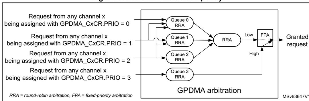
GPDMA arbitration
The GPDMA arbitration is directed from the 4-grade assigned channel priority (GPDMA_CxCR.PRIO[1:0]). The arbitration policy, as illustrated in Figure 59 , is defined by:
- • one high-priority traffic class (queue 3), dedicated to the assigned channels with priority 3, for time-sensitive channels
This traffic class is granted via a fixed-priority arbitration against any other low-priority traffic class. Within this class, requested single/burst transfers are round-robin arbitrated.
- • three low-priority traffic classes (queues 0, 1, or 2) for non time-sensitive channels with priority 0, 1, or 2
Each requested single/burst transfer within this class is round-robin arbitrated, with a weight that is monotonically driven from the programmed priority:
- – Requests with priority 0 are allocated to the queue 0.
- – Requests with priority 1 are allocated and replicated to the queue 0 and queue 1.
- – Requests with priority 2 are allocated and replicated to the queue 0, queue 1, and queue 2.
- – Any queue 0, 1, or 2 equally grants any of its active input requests in a round-robin manner, provided there are simultaneous requests.
- – Additionally, there is a second stage for the low-traffic with a round-robin arbiter that fairly alternates between simultaneous selected requests from queue 0, queue 1, and queue 2.
Figure 59. GPDMA arbitration policy
Request from any channel x being assigned with GPDMA_CxCR.PRIO = 0
Request from any channel x being assigned with GPDMA_CxCR.PRIO = 1
Request from any channel x being assigned with GPDMA_CxCR.PRIO = 2
Request from any channel x being assigned with GPDMA_CxCR.PRIO = 3
Queue 0 RRA
Queue 1 RRA
Queue 2 RRA
Queue 3 RRA
RRA
Low
High
FPA
Granted request
GPDMA arbitration
RRA = round-robin arbitration, FPA = fixed-priority arbitration
MSV63647V1
GPDMA arbitration and bandwidth
With this arbitration policy, the following is guaranteed:
- • Equal maximum bandwidth between requests with same priority
- • Reserved bandwidth (noted as \( B_{Q3} \) ) to the time-sensitive requests (with priority 3)
- • Residual weighted bandwidth between different low-priority requests (priority 0 versus priority 1 versus priority 2).
The two following examples highlight that the weighted round-robin arbitration is driven by the programmed priorities:
- •
Example 1:
basic application with two non time-sensitive GPDMA requests: req0 and req1. There are the following programming possibilities:
- – If they are assigned with same priority, the allocated bandwidth by the arbiter to req0 (
\(
B_{req0}
\)
) is
equal
to the allocated bandwidth to req1 (
\(
B_{req1}
\)
).\[ B_{req0} = B_{req1} = 1/2 * (1 - B_{Q3}) \]
- – If req0 is assigned to priority 0 and req1 to priority 1, the allocated bandwidth to req0 (
\(
B_{P0}
\)
) is
3 times less
than the allocated bandwidth to req1 (
\(
B_{P1}
\)
).\[ B_{req0} = B_{P0} = 1/2 * 1/2 * (1 - B_{Q3}) = 1/4 * (1 - B_{Q3}) \]\[ B_{req1} = B_{P1} = (1/2 + 1) * 1/2 * (1 - B_{Q3}) = 3/4 * (1 - B_{Q3}) \]
- – If req0 is assigned to priority 0 and req1 to priority 2, the allocated bandwidth to req0 (
\(
B_{P0}
\)
) is
5 times less
than the allocated bandwidth to req1 (
\(
B_{P2}
\)
).\[ B_{req0} = B_{P0} = 1/2 * 1/3 * (1 - B_{Q3}) = 1/6 * (1 - B_{Q3}) \]\[ B_{req1} = B_{P2} = (1/2 + 1 + 1) * 1/3 * (1 - B_{Q3}) = 5/6 * (1 - B_{Q3}) \]
- – If they are assigned with same priority, the allocated bandwidth by the arbiter to req0 (
\(
B_{req0}
\)
) is
equal
to the allocated bandwidth to req1 (
\(
B_{req1}
\)
).
The above computed bandwidth calculation is based on a theoretical input request, always active for any GPDMA clock cycle. This computed bandwidth from the arbiter must be weighted by the frequency of the request given by the application, that cannot be always active and may be quite much variable from one GPDMA client (example I2C at 400 kHz) to another one (PWM at 1 kHz) than the above x3 and x5 ratios.
- Example 2:
application where the user distributes a same non-null N number of GPDMA requests to every non time-sensitive priority 0, 1 and 2. The bandwidth calculation is then the following:
- – The allocated bandwidth to the set of requests of priority 0 (
\(
B_{P0}
\)
) is\[ B_{P0} = 1/3 * 1/3 * (1 - B_{Q3}) = 1/9 * (1 - B_{Q3}) \]
- – The allocated bandwidth to the set of requests of priority 1 (
\(
B_{P1}
\)
) is\[ B_{P1} = (1/3 + 1/2) * 1/3 * (1 - B_{Q3}) = 5/18 * (1 - B_{Q3}) \]
- – The allocated bandwidth to the set of requests of priority 2 (
\(
B_{P2}
\)
) is\[ B_{P2} = (1/3 + 1/2 + 1) * 1/3 * (1 - B_{Q3}) = 11/18 * (1 - B_{Q3}) \]
- – The allocated bandwidth to any request n ( \( B_n \) ) among the N requests of that priority \( P_i \) ( \( i = 0 \) to \( 2 \) ) is \( B_n = 1/N * B_{P_i} \)
- – The allocated bandwidth to any request n of priority
\(
0_i
\)
(
\(
B_{n, P_i}
\)
) is\[ B_{n, P0} = 1/N * 1/9 * (1 - B_{Q3}) \]\[ B_{n, P1} = 1/N * 5/18 * (1 - B_{Q3}) \]\[ B_{n, P2} = 1/N * 11/18 * (1 - B_{Q3}) \]
- – The allocated bandwidth to the set of requests of priority 0 (
\(
B_{P0}
\)
) is
In this example, when the master port bus bandwidth is not totally consumed by the time-sensitive queue 3, the residual bandwidth is such that 2.5 times less bandwidth is allocated to any request of priority 0 versus priority 1, and 5.5 times less bandwidth is allocated to any request of priority 0 versus priority 2.
More generally, assume that the following requests are present:
- • I requests (
\(
I \geq 0
\)
) assigned to priority 0
If \( I > 0 \) , these requests are noted from \( i = 0 \) to \( I-1 \) . - • J requests (
\(
J \geq 0
\)
) assigned to priority 1
If \( J > 0 \) , these requests are noted from \( j = 0 \) to \( J-1 \) . - • K requests (
\(
K > 0
\)
) assigned to priority 2
These requests are noted from \( k = 0 \) to \( K-1 \) - • L requests (
\(
L \geq 0
\)
) assigned to priority 3
If \( L > 0 \) , these requests are noted from \( l = 0 \) to \( L-1 \) .
As \( B_{Q3} \) is the reserved bandwidth to time-sensitive requests, the bandwidth for each request L with priority 3 is:
- • \( B_l = B_{Q3} / L \) for \( L > 0 \) (else: \( B_l = 0 \) )
The bandwidth for each non-time sensitive queue is:
- • \( B_{Q0} = 1/3 * (1 - B_{Q3}) \)
- • \( B_{Q1} = 1/3 * (1 - B_{Q3}) \)
- • \( B_{Q2} = 1/3 * (1 - B_{Q3}) \)
The bandwidth for the set of requests with priority 0 is:
- • \( B_{P0} = I / (I + J + K) * B_{Q0} \)
The bandwidth for each request i with priority 0 is:
- • \( B_i = B_{P0} / I \) for \( L > 0 \) (else \( B_{P0} = 0 \) )
The bandwidth for the set of requests with priority 1 and routed to queue 0 is:
- • \( B_{P1,Q0} = J / (I + J + K) * B_{Q0} \)
The bandwidth for the set of requests with priority 1 and routed to queue 1 is:
- \( B_{P1,Q1} = J / (J + K) * B_{Q1} \)
The total bandwidth for the set of requests with priority 1 is:
- \( B_{P1} = B_{P1,Q0} + B_{P1,Q1} \)
The bandwidth for each request j with priority 1 is:
- \( B_j = B_{P1} / J \) for \( J > 0 \) (else \( B_j = 0 \) )
The bandwidth for the set of requests with priority 2 and routed to queue 0 is:
- \( B_{P2,Q0} = K / (I + J + K) * B_{Q0} \)
The bandwidth for the set of requests with priority 2 and routed to queue 1 is:
- \( B_{P2,Q1} = K / (J + K) * B_{Q1} \)
The bandwidth for the set of requests with priority 2 and routed to queue 2 is:
- \( B_{P2,Q2} = B_{Q2} \)
The total bandwidth for the set of requests with priority 2 is:
- \( B_{P2} = B_{P2,Q0} + B_{P2,Q1} + B_{P2,Q2} \)
The bandwidth for each request k with priority 2 is:
- \( B_k = B_{P2} / K \) ( \( K > 0 \) in the general case)
Thus finally the maximum allocated residual bandwidths for any i, j, k non-time sensitive request are:
- in the general case (when there is at least one request k with a priority 2 (
\(
K > 0
\)
)):
- \( B_i = 1/I * 1/3 * I/(I + J + K) * (1 - B_{Q3}) \)
- \( B_j = 1/J * 1/3 * [J/(I + J + K) + J/(J + K)] * (1 - B_{Q3}) \)
- \( B_k = 1/K * 1/3 * [K/(I + J + K) + K/(J + K) + 1] * (1 - B_{Q3}) \)
- in the specific case (when there is no request k with a priority 2 (
\(
K = 0
\)
)):
- \( B_i = 1/I * 1/2 * I/(I + J) * (1 - B_{Q3}) \)
- \( B_j = 1/J * 1/2 * [J/(I + J) + 1] * (1 - B_{Q3}) \)
Consequently, the GPDMA arbiter can be used as a programmable weighted bandwidth limiter, for each queue and more generally for each request/channel. The different weights are monotonically resulting from the programmed channel priorities.
15.4.12 GPDMA triggered transfer
A programmed GPDMA transfer can be triggered by a rising/falling edge of a selected input trigger event, as defined by GPDMA_CxTR2.TRIGPOL[1:0] and GPDMA_CxTR2.TRIGSEL[5:0] (see Section 15.3.6 for the trigger selection).
The triggered transfer, as defined by the trigger mode in GPDMA_CxTR2.TRIGM[1:0], can be at LLI data transfer level, to condition the first burst read of a block, the first burst read of a 2D/repeated block for channel x ( \( x = 10 \) to \( 11 \) ), or each programmed single read. The trigger mode can also be programmed to condition the LLI link transfer (see TRIGM[1:0] in GPDMA_CxTR2 for more details).
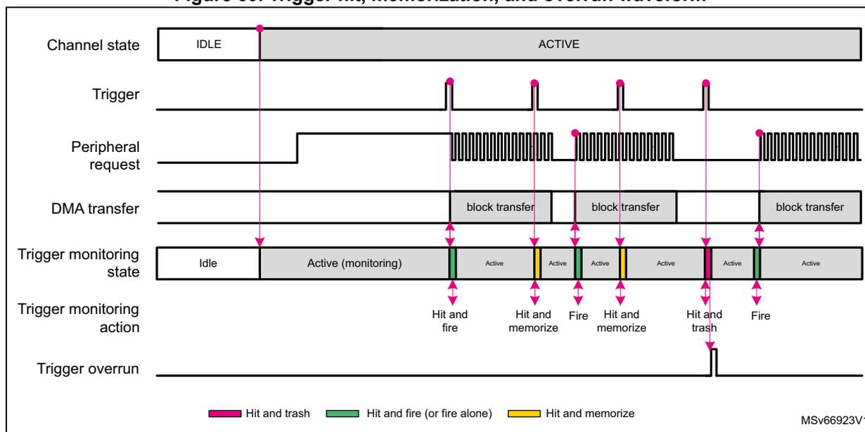
Trigger hit memorization and trigger overrun flag generation
The GPDMA monitoring of a trigger for a channel x is started when the channel is enabled/loaded with a new active trigger configuration: rising or falling edge on a selected trigger (respectively TRIGPOL[1:0] = 01 or TRIGPOL[1:0] = 10).
The monitoring of this trigger is kept active during the triggered and uncompleted (data or link) transfer. If a new trigger is detected, this hit is internally memorized to grant the next transfer, as long as the defined rising/falling edge and TRIGSEL[5:0] are not modified, and the channel is enabled.
Transferring a next \( LLI_{n+1} \) , that updates the GPDMA_CxTR2 with a new value for any of TRIGSEL[5:0] or TRIGPOL[1:0], resets the monitoring, trashing the possible memorized hit of the formerly defined \( LLI_n \) trigger.
Caution: After a first new trigger hit n+1 is memorized, if another trigger hit n+2 is detected and if the hit n triggered transfer is still not completed, hit n+2 is lost and not memorized. A trigger overrun flag is reported (GPDMA_CxSR.TOF = 1) and an interrupt is generated if enabled (if GPDMA_CxCR.TOIE = 1). The channel is not automatically disabled by hardware due to a trigger overrun.
Figure 60 illustrates the trigger hit, memorization and overrun in the configuration example with a block-level trigger mode and a rising edge trigger polarity.
Figure 60. Trigger hit, memorization, and overrun waveform
Note: The user can assign the same input trigger event to different channels. This can be used to trigger different channels on a broadcast trigger event.
15.4.13 GPDMA circular buffering with linked-list programming
GPDMA circular buffering for memory-to-peripheral and peripheral-to-memory transfers, with a linear addressing channel
For a circular buffering, with a continuous memory-to-peripheral (or peripheral-to-memory) transfer, the software must set up a channel with half-transfer and complete transfer interrupts.
events/interrupts generation (GPDMA_CxCR.HTIE = 1 and GPDMA_CxCR.TCIE = 1), in order to enable a concurrent buffer software processing.
LLI 0 is configured for the first block transfer with the linear addressing channel. A continuously-executed LLI 1 is needed to restore the memory source (or destination) start address, for the memory-to-peripheral transfer (respectively the peripheral-to-memory transfer). GPDMA automatically reloads the initially programmed GPDMA_CxBR1.BNDT[15:0] when a block transfer is completed, and there is no need to restore GPDMA_CxBR1.
Figure 61 illustrates this programming with a linear addressing GPDMA channel and a source circular buffer.
Figure 61. GPDMA circular buffer programming: update of the memory start address with a linear addressing channel
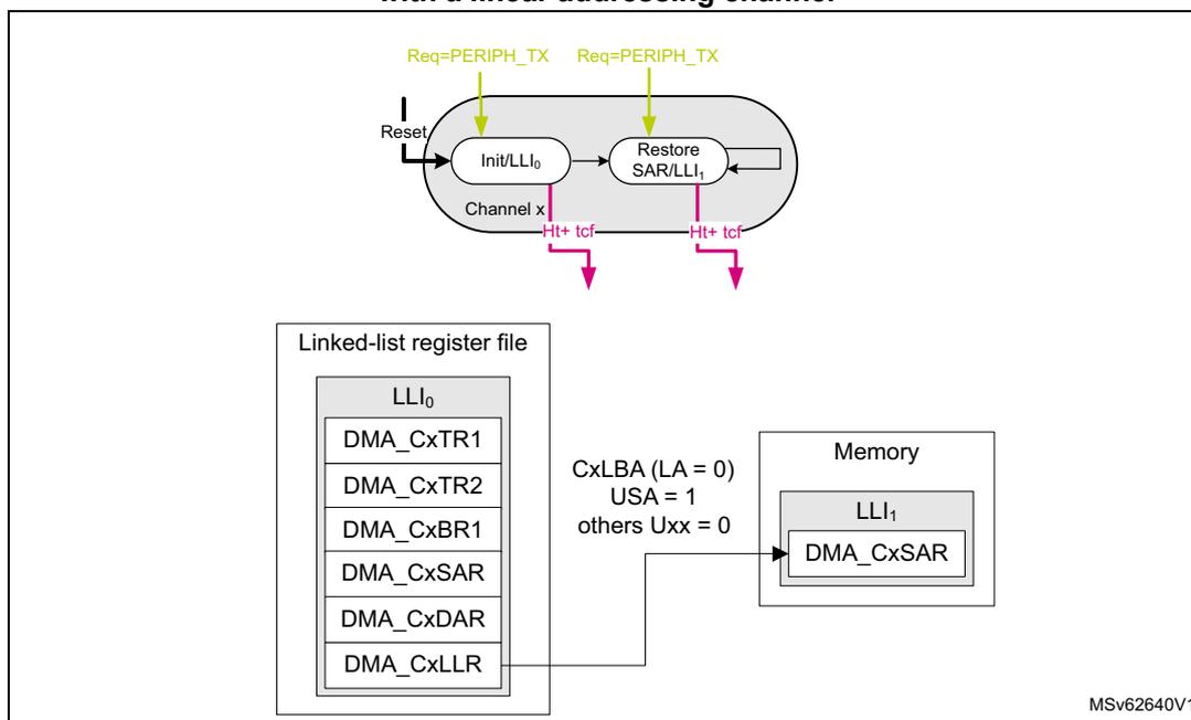
Note:
With a 2D addressing channel, the user may use a single LLI with GPDMA_CxBR1.BRC[10:0] = 1, and program a negative memory block address offset with GPDMA_CxBR2 and GPDMA_CxBR1, in order to jump back to the memory source or the destination start address.
If circular buffering must be executed after some other transfers over the shared GPDMA channel x, the before-last LLI N-1 in memory is needed to configure the first block transfer. And the last LLI N restores the memory source (or destination) start address in memory-to-peripheral transfer (respectively in peripheral-to-memory transfer).
Figure 62 illustrates this programming with a linear addressing shared GPDMA channel, and a source circular buffer.
Figure 62. Shared GPDMA channel with circular buffering: update of the memory start address with a linear addressing channel
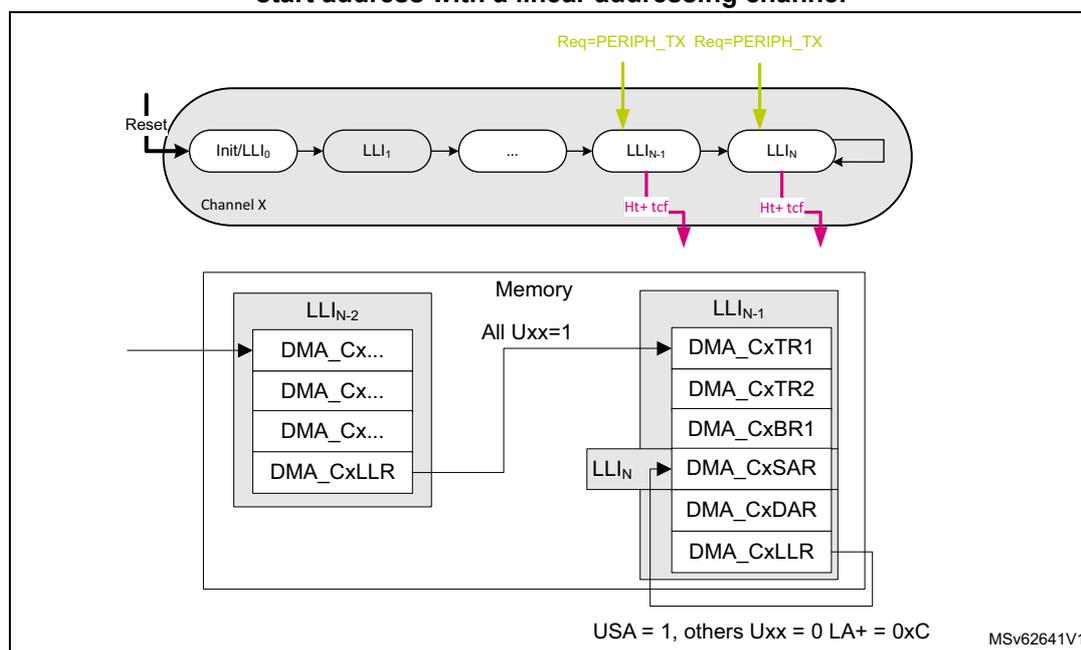
15.4.14 GPDMA transfer in peripheral flow-control mode
A peripheral with the peripheral flow-control mode feature can decide to early terminate a GPDMA block transfer, provided that the allocated channel is implemented with this feature (see Section 15.3.5 ).
If the related GPDMA channel x is also programmed in peripheral flow-control mode (GPDMA_CxTR2.PFREQ = 1):
- • The GPDMA block transfer starts as follows:
- – If GPDMA_CxBR1.BNDT[15:0] \( \neq \) 0, the programmed value is internally taken into account by the GPDMA hardware.
- – If GPDMA_CxBR1.BNDT[15:0] = 0, the GPDMA hardware internally considers a 64-Kbyte value for the maximum source block size to be transferred.
- • The GPDMA block transfer is completed as soon as the first occurrence of one of the following condition occurs:
- – when GPDMA_CxBR1.BNDT[15:0] = 0
- – when the peripheral early terminates the block. The complete transfer event is generated if programmed, depending on GPDMA_CxTR2 (see GPDMA channel x transfer register 2 (GPDMA_CxTR2) ). Then the software can read the current number of transferred bytes from the source (GPDMA_CxBR1.BNDT[15:0]), and/or read the current source or destination address of the buffer in memory (GPDMA_CxSAR[31:0] or GPDMA_CxDAR[31:0]).
In peripheral flow-control mode:
- • a destination peripheral with a hardware requested transfer is not supported: memory-to-peripheral transfer is not supported.
- • Data packing from a source peripheral is not supported.
- • 2D/repeated block is not supported.
- • GPDMA_CxBR1.BNDT[15:0] must be programmed as a multiple of the source (peripheral) burst size.
15.4.15 GPDMA secure/nonsecure channel
The GPDMA controller is compliant with the TrustZone hardware architecture at channel level, partitioning all its resources so that they exist in one of the secure and nonsecure worlds at any given time.
Any channel x is a secure or a nonsecure hardware resource, as configured by GPDMA_SECCFGR.SECx.
When a channel x is configured in secure state by a secure and privileged agent, the following access control rules are applied:
- • A nonsecure read access to a register field of this channel is forced to return 0, except for GPDMA_SECCFGR, GPDMA_PRIVCFGR, GPDMA_RCFGLOCKR that are readable by a nonsecure agent.
- • A nonsecure write access to a register field of this channel has no impact.
When a channel x is configured in secure state, a secure agent can configure separately as secure or nonsecure the GPDMA data transfer from the source (GPDMA_CxTR1.SSEC) and the GPDMA data transfer to the destination (GPDMA_CxTR1.DSEC).
When a channel x is configured in secure state and in linked-list mode, the loading of the next linked-list data structure from the GPDMA memory into its register file, is automatically performed with secure transfers via the GPDMA_CxCR.LAP allocated master port.
The GPDMA generates a secure bus that reflects GPDMA_SECCFGR, to keep the other peripherals informed of the secure/nonsecure state of each GPDMA channel x.
The GPDMA also generates a security illegal access pulse signal on an illegal nonsecure access to a secure GPDMA register. This signal is routed to the TrustZone interrupt controller.
When the secure software must switch a channel from a secure state to a nonsecure state, the secure software must abort the channel or wait until the secure channel is completed before switching. This is needed to dynamically re-allocate a channel to a next nonsecure transfer as a nonsecure software is not allowed to do so and must have GPDMA_CxCR.EN = 0 before the nonsecure software can reprogram the GPDMA_CxCR for a next transfer. The secure software may reset not only the channel x (GPDMA_CxCR.RESET = 1) but also the full channel x register file to its reset value.
15.4.16 GPDMA privileged/unprivileged channel
Any channel x is a privileged or unprivileged hardware resource, as configured by a privileged agent via GPDMA_PRIVCFGR.PRIVx.
When a channel x is configured in a privileged state by a privileged agent, the following access control rules are applied:
- • An unprivileged read access to a register field of this channel is forced to return 0, except for GPDMA_PRIVCFGR, GPDMA_SECCFGR, GPDMA_RCFGLOCKR that are readable by an unprivileged agent.
- • An unprivileged write access to a register field of this channel has no impact.
When a channel is configured in a privileged (or unprivileged) state, the source and destination data transfers are privileged (respectively unprivileged) transfers over the AHB master port.
When a channel is configured in a privileged (or unprivileged) state and in linked-list mode, the loading of the next linked-list data structure from the GPDMA memory into its register file, is automatically performed with privileged (respectively unprivileged) transfers, via the GPDMA_CxCR.LAP allocated master port.
The GPDMA generates a privileged bus that reflects GPDMA_PRIVCFGR, to keep the other peripherals informed of the privileged/unprivileged state of each GPDMA channel x.
When the privileged software must switch a channel from a privileged state to an unprivileged state, the privileged software must abort the channel or wait until that the privileged channel is completed before switching. This is needed to dynamically re-allocate a channel to a next unprivileged transfer as an unprivileged software is not allowed to do so, and must have GPDMA_CxCR.EN = 0 before the unprivileged software can reprogram the GPDMA_CxCR for a next transfer. The privileged software may reset not only the channel x (GPDMA_CxCR.RESET = 1) but also the full channel x register file to its reset value.
15.4.17 GPDMA error management
The GPDMA is able to manage and report to the user a transfer error, as follows, depending on the root cause.
Data transfer error
On a bus access (as a AHB single or a burst) to the source or the destination:
- • The source or destination target reports an AHB error.
- • The programmed channel transfer is stopped (GPDMA_CxCR.EN cleared by the GPDMA hardware). The channel status register reports an idle state (GPDMA_CxSR.IDLEF = 1) and the data error (GPDMA_CxSR.DTEF = 1).
- • After a GPDMA data transfer error, the user must perform a debug session, taking care of the product-defined memory mapping of the source and destination, including the protection attributes.
- • After a GPDMA data transfer error, the user must issue a channel reset (set GPDMA_CxCR.RESET) to reset the hardware GPDMA channel data path and the content of the FIFO, before the user enables again the same channel for a next transfer.
Link transfer error
On a tentative update of a GPDMA channel register from the programmed LLI in the memory:
- • The linked-list memory reports an AHB error.
- • The programmed channel transfer is stopped (GPDMA_CxCR.EN cleared by the GPDMA hardware), the channel status register reports an idle state (GPDMA_CxSR.IDLEF = 1) and the link error (GPDMA_CxSR.ULEF = 1).
- • After a GPDMA link error, the user must perform a debug session, taking care of the product-defined memory mapping of the linked-list data structure (GPDMA_CxLBAR and GPDMA_CxLLR), including the protection attributes.
- • After a GPDMA link error, the user must explicitly write the linked-list register file (GPDMA_CxTR1, GPDMA_CxTR2, GPDMA_CxBR1, GPDMA_CxSAR, GPDMA_CxDAR and GPDMA_CxLLR, plus GPDMA_CxTR3 and GPDMA_CxBR2), before the user enables again the same channel for a next transfer.
User setting error
On a tentative execution of a GPDMA transfer with an unauthorized user setting:
- • The programmed channel transfer is disabled (GPDMA_CxCR.EN forced and cleared by the GPDMA hardware) preventing the next unauthorized programmed data transfer from being executed. The channel status register reports an idle state (GPDMA_CxSR.IDLEF = 1) and a user setting error (GPDMA_CxSR.USEF = 1).
- • After a GPDMA user setting error, the user must perform a debug session, taking care of the GPDMA channel programming. A user setting error can be caused by one of the following:
- – a programmed null source block size without a programmed update of this value from the next LLI 1 (GPDMA_CxBR1.BNDT[15:0] = 0 and GPDMA_CxLLR.UB1 = 0)
- – a programmed non-null source block size being not a multiple of the programmed data width of a source burst transfer (GPDMA_CxBR1.BNDT[2:0] versus GPDMA_CxTR1.SDW_LOG2[1:0])
- – when in packing/unpacking mode (if PAM[1] = 1), a programmed non-null source block size being not a multiple of the programmed data width of a destination burst transfer (GPDMA_CxBR1.BNDT[2:0] versus GPDMA_CxTR1.DDW_LOG2[1:0])
- – a programmed unaligned source start address, being not a multiple of the programmed data width of a source burst transfer (GPDMA_CxSAR[2:0] versus GPDMA_CxTR1.SDW_LOG2[1:0])
- – for channel x (x = 10 to 11): a programmed unaligned source address offset being not a multiple of the programmed data width of a source burst transfer (GPDMA_CxTR3.SAO[2:0] versus GPDMA_CxTR1.SDW_LOG2[1:0])
- – for channel x (x = 10 to 11): a programmed unaligned block repeated source address offset being not a multiple of the programmed data width of a source burst transfer (GPDMA_CxBR2.BRSAO[2:0] versus GPDMA_CxTR1.SDW_LOG2[1:0])
- – a programmed unaligned destination start address, being not a multiple of the programmed data width of a destination burst transfer (GPDMA_CxDAR[2:0] versus GPDMA_CxTR1.DDW_LOG2[1:0])
- – for channel x (x = 10 to 11): a programmed unaligned destination address offset being not a multiple of the programmed data width of a destination burst transfer (GPDMA_CxTR3.DAO[2:0] versus GPDMA_CxTR1.DDW_LOG2[1:0])
- – for channel x (x = 10 to 11): a programmed unaligned block repeated destination address offset being not a multiple of the programmed data width of a destination burst transfer (GPDMA_CxBR2.BRDAO[2:0] versus GPDMA_CxTR1.DDW_LOG2[1:0])
- – a programmed double-word source data width (GPDMA_CxTR1.SDW_LOG2[1:0] = 11)
- – a programmed double-word destination data width (GPDMA_CxTR1.DDW_LOG2[1:0] = 11)
- – a programmed linked-list item \( LLI_{n+1} \) with a null data transfer (GPDMA_CxLLR.UB1 = 1 and GPDMA_CxBR1.BNDT = 0)
15.5 GPDMA in debug mode
When the microcontroller enters debug mode (core halted), any channel x can be individually either continued (default) or suspended, depending on the programmable control bit in the DBGMCU module.
Note: In debug mode, GPDMA_CxSR.SUSPF is not altered by a suspension from the programmable control bit in the DBGMCU module. In this case, GPDMA_CxSR.IDLEF can be checked to know the completion status of the channel suspension.
15.6 GPDMA in low-power modes
Table 131. Effect of low-power modes on GPDMA
| Mode | Description |
|---|---|
| Sleep | No effect. GPDMA interrupts cause the device to exit Sleep mode. |
| Stop (1) | The content of the GPDMA registers is kept when entering Stop mode. |
| Standby | The GPDMA is powered down and must be reinitialized after exiting Standby mode. |
1. Refer to Section 15.3.2 to know if any Stop mode is supported.
15.7 GPDMA interrupts
There is one GPDMA interrupt line for each channel, and separately for each CPU (if several ones in the devices).
Table 132. GPDMA interrupt requests
| Interrupt acronym | Interrupt event | Interrupt enable | Event flag | Event clear method |
|---|---|---|---|---|
| GPDMA_CHx | Transfer complete | GPDMA_CxCR.TCIE | GPDMA_CxSR.TCF | Write 1 to GPDMA_CxFCR.TCF |
| Half transfer | GPDMA_CxCR.HTIE | GPDMA_CxSR.HTF | Write 1 to GPDMA_CxFCR.HTF | |
| Data transfer error | GPDMA_CxCR.DTEIE | GPDMA_CxSR.DTEF | Write 1 to GPDMA_CxFCR.DTEF | |
| Update link error | GPDMA_CxCR.ULEIE | GPDMA_CxSR.ULEF | Write 1 to GPDMA_CxFCR.ULEF | |
| User setting error | GPDMA_CxCR.USEIE | GPDMA_CxSR.USEF | Write 1 to GPDMA_CxFCR.USEF | |
| Suspended | GPDMA_CxCR.SUSPIE | GPDMA_CxSR.SUSPF | Write 1 to GPDMA_CxFCR.SUSPF | |
| Trigger overrun | GPDMA_CxCR.TOFIE | GPDMA_CxSR.TOF | Write 1 to GPDMA_CxFCR.TOF |
A GPDMA channel x event may be:
- • a transfer complete
- • a half-transfer complete
- • a transfer error, due to either:
- – a data transfer error
- – an update link error
- – a user setting error completed suspension
- • a trigger overrun
Note: When a channel x transfer complete event occurs, the output signal gpdma_chx_tc is generated as a high pulse of one clock cycle.
An interrupt is generated following any xx event, provided that both:
- • the corresponding interrupt event xx is enabled (GPDMA_CxCR.xxIE = 1)
- • the corresponding event flag is cleared (GPDMA_CxSR.xxF = 0). This means that, after a previous same xx event occurrence, a software agent must have written 1 into the corresponding xx flag clear control bit (write 1 into GPDMA_CxFCR.xxF).
TCF (transfer complete) and HTF (half transfer) events generation is controlled by GPDMA_CxTR2.TCEM[1:0] as follows:
- • A transfer complete event is a block transfer complete, a 2D/repeated block transfer complete, or a LLI transfer complete including the upload of the next LLI if any, or the full linked-list completion, depending on the transfer complete event mode GPDMA_CxTR2.TCEM[1:0].
- • A half-transfer event is a half-block transfer or a half 2D/repeated block transfer, depending on the transfer complete event mode GPDMA_CxTR2.TCEM[1:0].
A half-block transfer occurs when half of the source block size bytes (rounded-up integer of GPDMA_CxBR1.BNDT[15:0] / 2) is transferred to the destination.
A half 2D/repeated block transfer occurs when half of the repeated blocks (rounded-up integer of (GPDMA_CxBR1.BRC[10:0] + 1) / 2) is transferred to the destination.
See GPDMA channel x transfer register 2 (GPDMA_CxTR2) for more details.
A transfer error rises in one of the following situations:
- • during a single/burst data transfer from the source or to the destination (DTEF)
- • during an update of a GPDMA channel register from the programmed LLI in memory (ULEF)
- • during a tentative execution of a GPDMA channel with an unauthorized setting (USEF)
- The user must perform a debug session to correct the GPDMA channel programming versus the USEF root causes list (see Section 15.4.17 ).
A trigger overrun is described in Trigger hit memorization and trigger overrun flag generation .
15.8 GPDMA registers
The GPDMA registers must be accessed with an aligned 32-bit word data access.
15.8.1 GPDMA secure configuration register (GPDMA_SECCFGR)
Address offset: 0x00
Reset value: 0x0000 0000
A write access to this register must be secure and privileged. A read access is secure or nonsecure, privileged or unprivileged.
A write access is ignored at bit level if the corresponding channel x is locked (GPDMA_RCFGLOCKR.LOCKx = 1).
This register must be written when GPDMA_CxCR.EN = 0.
This register is read-only when GPDMA_CxCR.EN = 1.
This register must be programmed at a bit level, at the initialization/closure of a GPDMA channel (when GPDMA_CxCR.EN = 0), to securely allocate individually any channel x to the secure or nonsecure world.
| 31 | 30 | 29 | 28 | 27 | 26 | 25 | 24 | 23 | 22 | 21 | 20 | 19 | 18 | 17 | 16 |
|---|---|---|---|---|---|---|---|---|---|---|---|---|---|---|---|
| Res. | Res. | Res. | Res. | Res. | Res. | Res. | Res. | Res. | Res. | Res. | Res. | Res. | Res. | Res. | Res. |
| 15 | 14 | 13 | 12 | 11 | 10 | 9 | 8 | 7 | 6 | 5 | 4 | 3 | 2 | 1 | 0 |
| Res. | Res. | Res. | Res. | SEC11 | SEC10 | SEC9 | SEC8 | SEC7 | SEC6 | SEC5 | SEC4 | SEC3 | SEC2 | SEC1 | SEC0 |
| rw | rw | rw | rw | rw | rw | rw | rw | rw | rw | rw | rw |
Bits 31:12 Reserved, must be kept at reset value.
Bits 11:0 SECx : secure state of channel x (x = 11 to 0)
0: Nonsecure
1: Secure
15.8.2 GPDMA privileged configuration register (GPDMA_PRIVCFGR)
Address offset: 0x04
Reset value: 0x0000 0000
A write access to this register must be privileged. A read access can be privileged or unprivileged, secure or nonsecure.
This register can mix secure and nonsecure information. If a channel x is configured as secure (GPDMA_SECCFGR.SECx = 1), the PRIVx bit can be written only by a secure (and privileged) agent.
A write access is ignored at bit level if the corresponding channel x is locked (GPDMA_RCFGLOCKR.LOCKx = 1).
This register must be written when GPDMA_CxCR.EN = 0.
This register is read-only when GPDMA_CxCR.EN = 1.
This register must be programmed at a bit level, at the initialization/closure of a GPDMA channel (GPDMA_CxCR.EN = 0), to individually allocate any channel x to the privileged or unprivileged world.
| 31 | 30 | 29 | 28 | 27 | 26 | 25 | 24 | 23 | 22 | 21 | 20 | 19 | 18 | 17 | 16 |
|---|---|---|---|---|---|---|---|---|---|---|---|---|---|---|---|
| Res. | Res. | Res. | Res. | Res. | Res. | Res. | Res. | Res. | Res. | Res. | Res. | Res. | Res. | Res. | Res. |
| 15 | 14 | 13 | 12 | 11 | 10 | 9 | 8 | 7 | 6 | 5 | 4 | 3 | 2 | 1 | 0 |
| Res. | Res. | Res. | Res. | PRIV11 | PRIV10 | PRIV9 | PRIV8 | PRIV7 | PRIV6 | PRIV5 | PRIV4 | PRIV3 | PRIV2 | PRIV1 | PRIV0 |
| rw | rw | rw | rw | rw | rw | rw | rw | rw | rw | rw | rw |
Bits 31:12 Reserved, must be kept at reset value.
Bits 11:0 PRIVx : privileged state of channel x (x = 11 to 0)
0: unprivileged
1: privileged
15.8.3 GPDMA configuration lock register (GPDMA_RCFGLOCKR)
Address offset: 0x08
Reset value: 0x0000 0000
This register can be written by a software agent with secure privileged attributes in order to individually lock, for example at boot time, the secure privileged attributes of any GPDMA
channel/resource (to lock the setting of GPDMA_CxSECCFGR, GPDMA_CxPRIVCFGR for any channel x, for example at boot time).
A read access may be privileged or unprivileged, secure or nonsecure.
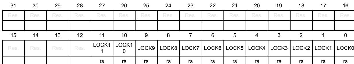
| 31 | 30 | 29 | 28 | 27 | 26 | 25 | 24 | 23 | 22 | 21 | 20 | 19 | 18 | 17 | 16 |
| Res. | Res. | Res. | Res. | Res. | Res. | Res. | Res. | Res. | Res. | Res. | Res. | Res. | Res. | Res. | Res. |
| 15 | 14 | 13 | 12 | 11 | 10 | 9 | 8 | 7 | 6 | 5 | 4 | 3 | 2 | 1 | 0 |
| Res. | Res. | Res. | Res. | LOCK1 1 | LOCK1 0 | LOCK9 | LOCK8 | LOCK7 | LOCK6 | LOCK5 | LOCK4 | LOCK3 | LOCK2 | LOCK1 | LOCK0 |
| rs | rs | rs | rs | rs | rs | rs | rs | rs | rs | rs | rs |
Bits 31:12 Reserved, must be kept at reset value.
Bits 11:0 LOCKx : lock the configuration of GPDMA_SECCFGR.SECx, GPDMA_PRIVCFGR.PRIVx until a global GPDMA reset (x = 11 to 0)
This bit is cleared after reset and, once set, it cannot be reset until a global GPDMA reset.
0: secure privilege configuration of the channel x is writable.
1: secure privilege configuration of the channel x is not writable.
15.8.4 GPDMA nonsecure masked interrupt status register (GPDMA_MISR)
Address offset: 0x0C
Reset value: 0x0000 0000
This register is a read register.
This is a nonsecure register, containing the masked interrupt status bit MISx for each nonsecure channel x (channel x configured with GPDMA_SECCFGR.SECx = 0). It is a logical OR of all the flags of GPDMA_CxSR, each source flag being enabled by the corresponding interrupt enable bit of GPDMA_CxCR.
Every bit is deasserted by hardware when writing 1 to the corresponding flag clear bit in GPDMA_CxFCR.
If a channel x is in secure state (GPDMA_SECCFGR.SECx = 1), a read access to the masked interrupt status bit MISx of this channel x returns zero.
This register may mix privileged and unprivileged information, depending on the privileged state of each channel GPDMA_PRIVCFGR.PRIVx. A privileged software can read the full nonsecure interrupt status. An unprivileged software is restricted to read the status of unprivileged (and nonsecure) channels, other privileged bit fields returning zero.
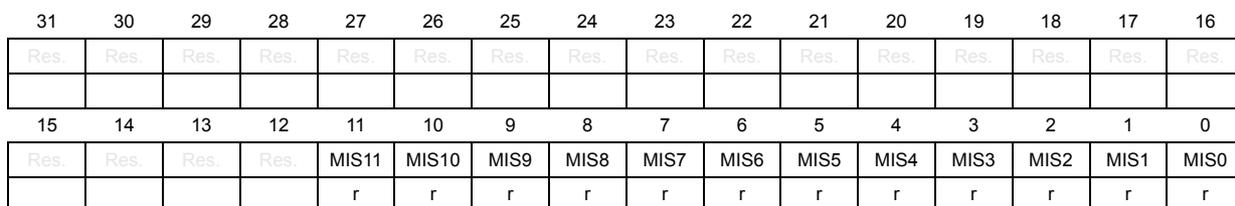
| 31 | 30 | 29 | 28 | 27 | 26 | 25 | 24 | 23 | 22 | 21 | 20 | 19 | 18 | 17 | 16 |
| Res. | Res. | Res. | Res. | Res. | Res. | Res. | Res. | Res. | Res. | Res. | Res. | Res. | Res. | Res. | Res. |
| 15 | 14 | 13 | 12 | 11 | 10 | 9 | 8 | 7 | 6 | 5 | 4 | 3 | 2 | 1 | 0 |
| Res. | Res. | Res. | Res. | MIS11 | MIS10 | MIS9 | MIS8 | MIS7 | MIS6 | MIS5 | MIS4 | MIS3 | MIS2 | MIS1 | MIS0 |
| r | r | r | r | r | r | r | r | r | r | r | r |
Bits 31:12 Reserved, must be kept at reset value.
Bits 11:0 MISx : masked interrupt status of channel x (x = 11 to 0)
0: no interrupt occurred on channel x
1: an interrupt occurred on channel x
15.8.5 GPDMA secure masked interrupt status register (GPDMA_SMISR)
Address offset: 0x10
Reset value: 0x0000 0000
This is a secure read register, containing the masked interrupt status bit MISx for each secure channel x (GPDMA_SECCFGR.SECx = 1). It is a logical OR of all the GPDMA_CxSR flags, each source flag being enabled by the corresponding GPDMA_CxCR interrupt enable bit.
Every bit is deasserted by hardware when securely writing 1 to the corresponding GPDMA_CxFCR flag clear bit.
This register does not contain any information about a nonsecure channel.
This register can mix privileged and unprivileged information, depending on the privileged state of each channel GPDMA_PRIVCFGR.PRIVx. A privileged software can read the full secure interrupt status. An unprivileged software is restricted to read the status of unprivileged and secure channels, other privileged bit fields returning zero.
| 31 | 30 | 29 | 28 | 27 | 26 | 25 | 24 | 23 | 22 | 21 | 20 | 19 | 18 | 17 | 16 |
|---|---|---|---|---|---|---|---|---|---|---|---|---|---|---|---|
| Res. | Res. | Res. | Res. | Res. | Res. | Res. | Res. | Res. | Res. | Res. | Res. | Res. | Res. | Res. | Res. |
| 15 | 14 | 13 | 12 | 11 | 10 | 9 | 8 | 7 | 6 | 5 | 4 | 3 | 2 | 1 | 0 |
| Res. | Res. | Res. | Res. | MIS11 | MIS10 | MIS9 | MIS8 | MIS7 | MIS6 | MIS5 | MIS4 | MIS3 | MIS2 | MIS1 | MIS0 |
| r | r | r | r | r | r | r | r | r | r | r | r |
Bits 31:12 Reserved, must be kept at reset value.
Bits 11:0 MISx : masked interrupt status of the secure channel x (x = 11 to 0)
0: no interrupt occurred on the secure channel x
1: an interrupt occurred on the secure channel x
15.8.6 GPDMA channel x linked-list base address register (GPDMA_CxLBAR)
Address offset: 0x50 + 0x80 * x (x = 0 to 11)
Reset value: 0x0000 0000
This register must be written by a privileged software. It is either privileged readable or not, depending on the privileged state of the channel x GPDMA_PRIVCFGR.PRIVx.
This register is either secure or nonsecure depending on the secure state of the channel x (GPDMA_SECCFGR.SECx).
This register must be written when GPDMA_CxCR.EN = 0.
This register is read-only when GPDMA_CxCR.EN = 1.
This channel-based register is the linked-list base address of the memory region, for a given channel x, from which the LLIs describing the programmed sequence of the GPDMA transfers, are conditionally and automatically updated.
This 64-Kbyte aligned channel x linked-list base address is offset by the 16-bit GPDMA_CxLLR register that defines the word-aligned address offset for each LLI.
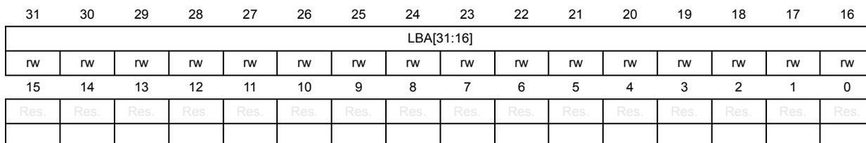
| 31 | 30 | 29 | 28 | 27 | 26 | 25 | 24 | 23 | 22 | 21 | 20 | 19 | 18 | 17 | 16 |
| LBA[31:16] | |||||||||||||||
| rw | rw | rw | rw | rw | rw | rw | rw | rw | rw | rw | rw | rw | rw | rw | rw |
| 15 | 14 | 13 | 12 | 11 | 10 | 9 | 8 | 7 | 6 | 5 | 4 | 3 | 2 | 1 | 0 |
| Res. | Res. | Res. | Res. | Res. | Res. | Res. | Res. | Res. | Res. | Res. | Res. | Res. | Res. | Res. | Res. |
Bits 31:16 LBA[31:16] : linked-list base address of GPDMA channel x
Bits 15:0 Reserved, must be kept at reset value.
15.8.7 GPDMA channel x flag clear register (GPDMA_CxFCR)
Address offset: 0x5C+ 0x80 * x (x = 0 to 11)
Reset value: 0x0000 0000
This is a write register, secure or nonsecure depending on the secure state of channel x (GPDMA_SECCFGR.SECx) and privileged or unprivileged, depending on the privileged state of the channel x (GPDMA_PRIVCFGR.PRIVx).
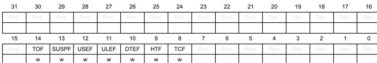
| 31 | 30 | 29 | 28 | 27 | 26 | 25 | 24 | 23 | 22 | 21 | 20 | 19 | 18 | 17 | 16 |
| Res. | Res. | Res. | Res. | Res. | Res. | Res. | Res. | Res. | Res. | Res. | Res. | Res. | Res. | Res. | Res. |
| 15 | 14 | 13 | 12 | 11 | 10 | 9 | 8 | 7 | 6 | 5 | 4 | 3 | 2 | 1 | 0 |
| Res. | TOF | SUSPF | USEF | ULEF | DTEF | HTF | TCF | Res. | Res. | Res. | Res. | Res. | Res. | Res. | Res. |
| w | w | w | w | w | w | w |
Bits 31:15 Reserved, must be kept at reset value.
Bit 14 TOF : trigger overrun flag clear
- 0: no effect
- 1: corresponding TOF flag cleared
Bit 13 SUSPF : completed suspension flag clear
- 0: no effect
- 1: corresponding SUSPF flag cleared
Bit 12 USEF : user setting error flag clear
- 0: no effect
- 1: corresponding USEF flag cleared
Bit 11 ULEF : update link transfer error flag clear
- 0: no effect
- 1: corresponding ULEF flag cleared
Bit 10 DTEF : data transfer error flag clear
0: no effect
1: corresponding DTEF flag cleared
Bit 9 HTF : half-transfer flag clear
0: no effect
1: corresponding HTF flag cleared
Bit 8 TCF : transfer complete flag clear
0: no effect
1: corresponding TCF flag cleared
Bits 7:0 Reserved, must be kept at reset value.
15.8.8 GPDMA channel x status register (GPDMA_CxSR)
Address offset: 0x60 + 0x80 * x (x = 0 to 11)
Reset value: 0x0000 0001
This is a read register, reporting the channel status.
This register is secure or nonsecure, depending on the secure state of channel x (GPDMA_SECCFGR.SECx), and privileged or unprivileged, depending on the privileged state of the channel (GPDMA_PRIVCFGR.PRIVx).
| 31 | 30 | 29 | 28 | 27 | 26 | 25 | 24 | 23 | 22 | 21 | 20 | 19 | 18 | 17 | 16 |
|---|---|---|---|---|---|---|---|---|---|---|---|---|---|---|---|
| Res. | Res. | Res. | Res. | Res. | Res. | Res. | Res. | FIFOL[7:0] | |||||||
| r | r | r | r | r | r | r | r | ||||||||
| 15 | 14 | 13 | 12 | 11 | 10 | 9 | 8 | 7 | 6 | 5 | 4 | 3 | 2 | 1 | 0 |
| Res. | TOF | SUSPF | USEF | ULEF | DTEF | HTF | TCF | Res. | Res. | Res. | Res. | Res. | Res. | Res. | IDLEF |
| r | r | r | r | r | r | r | r | ||||||||
Bits 31:24 Reserved, must be kept at reset value.
Bits 23:16 FIFOL[7:0] : monitored FIFO level
Number of available write beats in the FIFO, in units of the programmed destination data width (see GPDMA_CxTR1.DDW_LOG2[1:0], in units of bytes, half-words, or words).
Note: After having suspended an active transfer, the user may need to read FIFOL[7:0], additionally to GPDMA_CxBR1.BDNT[15:0] and GPDMA_CxBR1.BRC[10:0], to know how many data have been transferred to the destination. Before reading, the user may wait for the transfer to be suspended (GPDMA_CxSR.SUSPF = 1).
Bit 15 Reserved, must be kept at reset value.
Bit 14 TOF : trigger overrun flag
0: no trigger overrun event
1: a trigger overrun event occurred
Bit 13 SUSPF : completed suspension flag
0: no completed suspension event
1: a completed suspension event occurred
Bit 12 USEF : user setting error flag
0: no user setting error event
1: a user setting error event occurred
Bit 11 ULEF : update link transfer error flag
0: no update link transfer error event
1: a master bus error event occurred while updating a linked-list register from memory
Bit 10 DTEF : data transfer error flag
0: no data transfer error event
1: a master bus error event occurred on a data transfer
Bit 9 HTF : half-transfer flag
0: no half-transfer event
1: a half-transfer event occurred
A half-transfer event is either a half-block transfer or a half 2D/repeated block transfer, depending on the transfer complete event mode (GPDMA_CxTR2.TCEM[1:0]).
A half-block transfer occurs when half of the bytes of the source block size (rounded up integer of GPDMA_CxBR1.BNDT[15:0]/2) has been transferred to the destination.
A half 2D/repeated block transfer occurs when half of the repeated blocks (rounded up integer of (GPDMA_CxBR1.BRC[10:0] + 1) / 2)) has been transferred to the destination.
Bit 8 TCF : transfer complete flag
0: no transfer complete event
1: a transfer complete event occurred
A transfer complete event is either a block transfer complete, a 2D/repeated block transfer complete, or a LLI transfer complete including the upload of the next LLI if any, or the full linked-list completion, depending on the transfer complete event mode (GPDMA_CxTR2.TCEM[1:0]).
Bits 7:1 Reserved, must be kept at reset value.
Bit 0 IDLEF : idle flag
0: channel not in idle state
1: channel in idle state
This idle flag is deasserted by hardware when the channel is enabled (GPDMA_CxCR.EN = 1) with a valid channel configuration (no USEF to be immediately reported).
This idle flag is asserted after hard reset or by hardware when the channel is back in idle state (in suspended or disabled state).
15.8.9 GPDMA channel x control register (GPDMA_CxCR)
Address offset: 0x64 + 0x80 * x (x = 0 to 11)
Reset value: 0x0000 0000
This register is secure or nonsecure depending on the secure state of channel x (GPDMA_SECCFGR.SECx), and privileged or unprivileged, depending on the privileged state of the channel x (GPDMA_PRIVCFGR.PRIVx).
This register is used to control a channel (activate, suspend, abort or disable it).
| 31 | 30 | 29 | 28 | 27 | 26 | 25 | 24 | 23 | 22 | 21 | 20 | 19 | 18 | 17 | 16 |
|---|---|---|---|---|---|---|---|---|---|---|---|---|---|---|---|
| Res. | Res. | Res. | Res. | Res. | Res. | Res. | Res. | PRIO[1:0] | Res. | Res. | Res. | Res. | LAP | LSM | |
| rw | rw | rw | rw | ||||||||||||
| 15 | 14 | 13 | 12 | 11 | 10 | 9 | 8 | 7 | 6 | 5 | 4 | 3 | 2 | 1 | 0 |
|---|---|---|---|---|---|---|---|---|---|---|---|---|---|---|---|
| Res. | TOIE | SUSPI E | USEIE | ULEIE | DTEIE | HTIE | TCIE | Res. | Res. | Res. | Res. | Res. | SUSP | RESET | EN |
| rw | rw | rw | rw | rw | rw | rw | rw | w | rw |
Bits 31:24 Reserved, must be kept at reset value.
Bits 23:22 PRIO[1:0] : priority level of the channel x GPDMA transfer versus others
- 00: low priority, low weight
- 01: low priority, mid weight
- 10: low priority, high weight
- 11: high priority
Note: This bit must be written when EN = 0. This bit is read-only when EN = 1.
Bits 21:18 Reserved, must be kept at reset value.
Bit 17 LAP : linked-list allocated port
This bit is used to allocate the master port for the update of the GPDMA linked-list registers from the memory.
- 0: port 0 (AHB) allocated
- 1: port 1 (AHB) allocated
Note: This bit must be written when EN = 0. This bit is read-only when EN = 1.
Bit 16 LSM : Link step mode
- 0: channel executed for the full linked-list and completed at the end of the last LLI (GPDMA_CxLLR = 0). The 16 low-significant bits of the link address are null (LA[15:0] = 0) and all the update bits are null (UT1 = UB1 = UT2 = USA = UDA = ULL = 0 and UT3 = UB2 = 0). Then GPDMA_CxBR1.BNDT[15:0] = 0 and GPDMA_CxBR1.BRC[10:0] = 0.
- 1: channel executed once for the current LLI
First the (possible 1D/repeated) block transfer is executed as defined by the current internal register file until GPDMA_CxBR1.BNDT[15:0] = 0 and GPDMA_CxBR1.BRC[10:0] = 0.
Secondly the next linked-list data structure is conditionally uploaded from memory as defined by GPDMA_CxLLR. Then channel execution is completed.
Note: This bit must be written when EN = 0. This bit is read-only when EN = 1.
Bit 15 Reserved, must be kept at reset value.
Bit 14 TOIE : trigger overrun interrupt enable
- 0: interrupt disabled
- 1: interrupt enabled
Bit 13 SUSPIE : completed suspension interrupt enable
- 0: interrupt disabled
- 1: interrupt enabled
Bit 12 USEIE : user setting error interrupt enable
- 0: interrupt disabled
- 1: interrupt enabled
Bit 11 ULEIE : update link transfer error interrupt enable
- 0: interrupt disabled
- 1: interrupt enabled
Bit 10 DTEIE : data transfer error interrupt enable
- 0: interrupt disabled
- 1: interrupt enabled
Bit 9 HTIE : half-transfer complete interrupt enable
- 0: interrupt disabled
- 1: interrupt enabled
Bit 8 TCIE : transfer complete interrupt enable
0: interrupt disabled
1: interrupt enabled
Bits 7:3 Reserved, must be kept at reset value.
Bit 2 SUSP : suspend
Writing 1 into the field RESET (bit 1) causes the hardware to de-assert this bit, whatever is written into this bit 2. Else:
Software must write 1 in order to suspend an active channel (channel with an ongoing GPDMA transfer over its master ports).
The software must write 0 in order to resume a suspended channel, following the programming sequence detailed in Figure 44 .
0: write: resume channel, read: channel not suspended
1: write: suspend channel, read: channel suspended.
Bit 1 RESET : reset
This bit is write only. Writing 0 has no impact. Writing 1 implies the reset of the following: the FIFO, the channel internal state, SUSP and EN bits (whatever is written receptively in bit 2 and bit 0).
The reset is effective when the channel is in steady state, meaning one of the following:
- - active channel in suspended state (GPDMA_CxSR.SUSPF = 1 and GPDMA_CxSR.IDLEF = GPDMA_CxCR.EN = 1)
- - channel in disabled state (GPDMA_CxSR.IDLEF = 1 and GPDMA_CxCR.EN = 0).
After writing a RESET, to continue using this channel, the user must explicitly reconfigure the channel including the hardware-modified configuration registers (GPDMA_CxBR1, GPDMA_CxSAR, and GPDMA_CxDAR) before enabling again the channel (see the programming sequence in Figure 45 ).
0: no channel reset
1: channel reset
Bit 0 EN : enable
Writing 1 into the field RESET (bit 1) causes the hardware to de-assert this bit, whatever is written into this bit 0. Else:
this bit is deasserted by hardware when there is a transfer error (master bus error or user setting error) or when there is a channel transfer complete (channel ready to be configured, for example if LSM = 1 at the end of a single execution of the LLI).
Else, this bit can be asserted by software.
Writing 0 into this EN bit is ignored.
0: write: ignored, read: channel disabled
1: write: enable channel, read: channel enabled
15.8.10 GPDMA channel x transfer register 1 (GPDMA_CxTR1)
Address offset: 0x90 + 0x80 * x (x = 0 to 11)
Reset value: 0x0000 0000
This register is secure or nonsecure depending on the secure state of channel x (GPDMA_SECCFGR.SECx) except for secure DSEC and SSEC, privileged or unprivileged, depending on the privileged state of the channel x in GPDMA_PRIVCFGR.PRIVx.
This register controls the transfer of a channel x.
This register must be written when GPDMA_CxCR.EN = 0.
This register is read-only when GPDMA_CxCR.EN = 1.
This register must be written when the channel is completed. Then the hardware has deasserted GPDMA_CxCR.EN). A channel transfer can be completed and programmed at different levels: block, 2D/repeated block, LLI or full linked-list.
In linked-list mode, during the link transfer, this register is automatically updated by GPDMA from the memory if GPDMA_CxLLR.UT1 = 1.
| 31 | 30 | 29 | 28 | 27 | 26 | 25 | 24 | 23 | 22 | 21 | 20 | 19 | 18 | 17 | 16 |
|---|---|---|---|---|---|---|---|---|---|---|---|---|---|---|---|
| DSEC | DAP | Res. | Res. | DHX | DBX | DBL_1[5:0] | DINC | Res. | DDW_LOG2[1:0] | ||||||
| rw | rw | rw | rw | rw | rw | rw | rw | rw | rw | rw | rw | rw | |||
| 15 | 14 | 13 | 12 | 11 | 10 | 9 | 8 | 7 | 6 | 5 | 4 | 3 | 2 | 1 | 0 |
|---|---|---|---|---|---|---|---|---|---|---|---|---|---|---|---|
| SSEC | SAP | SBX | PAM[1:0] | Res. | SBL_1[5:0] | SINC | Res. | SDW_LOG2[1:0] | |||||||
| rw | rw | rw | rw | rw | rw | rw | rw | rw | rw | rw | rw | rw | rw | ||
Bit 31 DSEC : security attribute of the GPDMA transfer to the destination
If GPDMA_SECCFGR.SECx = 1 and the access is secure:
0: GPDMA transfer nonsecure
1: GPDMA transfer secure
This is a secure register bit. This bit can only be read by a secure software. This bit must be written by a secure software when GPDMA_SECCFGR.SECx = 1. A secure write is ignored when GPDMA_SECCFGR.SECx = 0.
When GPDMA_SECCFGR.SECx is deasserted, this DSEC bit is also deasserted by hardware (on a secure reconfiguration of the channel as nonsecure), and the GPDMA transfer to the destination is nonsecure.
Bit 30 DAP : destination allocated port
This bit is used to allocate the master port for the destination transfer
0: port 0 (AHB) allocated
1: port 1 (AHB) allocated
Note: This bit must be written when EN = 0. This bit is read-only when EN = 1.
Bits 29:28 Reserved, must be kept at reset value.
Bit 27 DHX : destination half-word exchange
If the destination data size is shorter than a word, this bit is ignored.
If the destination data size is a word:
0: no halfword-based exchanged within word
1: the two consecutive (post PAM) half-words are exchanged in each destination word.
Bit 26 DBX : destination byte exchange
If the destination data size is a byte, this bit is ignored.
If the destination data size is not a byte:
0: no byte-based exchange within half-word
1: the two consecutive (post PAM) bytes are exchanged in each destination half-word.
Bits 25:20 DBL_1[5:0] : destination burst length minus 1, between 0 and 63
The burst length unit is one data named beat within a burst. If DBL_1[5:0] = 0, the burst can be named as single. Each data/beat has a width defined by the destination data width DDW_LOG2[1:0].
Note: If a burst transfer crossed a 1-Kbyte address boundary on a AHB transfer, the GPDMA modifies and shortens the programmed burst into singles or bursts of lower length, to be compliant with the AHB protocol.
If a burst transfer is of length greater than the FIFO size of the channel x, the GPDMA modifies and shortens the programmed burst into singles or bursts of lower length, to be compliant with the FIFO size. Transfer performance is lower, with GPDMA re-arbitration between effective and lower singles/bursts, but the data integrity is guaranteed.
Bit 19 DINC : destination incrementing burst
0: fixed burst
1: contiguously incremented burst
The destination address, pointed by GPDMA_CxDAR, is kept constant after a burst beat/single transfer, or is incremented by the offset value corresponding to a contiguous data after a burst beat/single transfer.
Bit 18 Reserved, must be kept at reset value.
Bits 17:16 DDW_LOG2[1:0] : binary logarithm of the destination data width of a burst, in bytes
00: byte
01: half-word (2 bytes)
10: word (4 bytes)
11: user setting error reported and no transfer issued
Note: A destination burst transfer must have an aligned address with its data width (start address GPDMA_CxDAR[2:0] and if present address offset GPDMA_CxTR3.DAO[2:0], versus DDW_LOG2[1:0]). Otherwise a user setting error is reported and no transfer is issued.
When configured in packing mode (PAM[1] = 1 and destination data width different from source data width), a source block size must be a multiple of the destination data width (see GPDMA_CxBR1.BNDT[2:0] versus DDW_LOG2[1:0]). Else a user setting error is reported and none transfer is issued.
Setting a 8-byte data width causes a user setting error to be reported and none transfer is issued.
Bit 15 SSEC : security attribute of the GPDMA transfer from the source
If GPDMA_SECCFGR.SECx = 1 and the access is secure:
0: GPDMA transfer nonsecure
1: GPDMA transfer secure
This is a secure register bit. This bit can only be read by a secure software. This bit must be written by a secure software when GPDMA_SECCFGR.SECx = 1. A secure write is ignored when GPDMA_SECCFGR.SECx = 0.
When GPDMA_SECCFGR.SECx is deasserted, this SSEC bit is also deasserted by hardware (on a secure reconfiguration of the channel as nonsecure), and the GPDMA transfer from the source is nonsecure.
Bit 14 SAP : source allocated port
This bit is used to allocate the master port for the source transfer
0: port 0 (AHB) allocated
1: port 1 (AHB) allocated
Note: This bit must be written when EN = 0. This bit is read-only when EN = 1.
Bit 13 SBX : source byte exchange within the unaligned half-word of each source word
If the source data width is shorter than a word, this bit is ignored.
If the source data width is a word:
0: no byte-based exchange within the unaligned half-word of each source word
1: the two consecutive bytes within the unaligned half-word of each source word are exchanged.
Bits 12:11 PAM[1:0] : padding/alignment mode
If \( DDW\_LOG2[1:0] = SDW\_LOG2[1:0] \) : if the data width of a burst destination transfer is equal to the data width of a burst source transfer, these bits are ignored.
Else, in the following enumerated values, the condition \( PAM\_1 \) is when destination data width is higher than source data width, and the condition \( PAM\_2 \) is when source data width is higher than destination data width.
Condition: \( PAM\_1 \)
00: source data is transferred as right aligned, padded with 0s up to the destination data width
01: source data is transferred as right aligned, sign extended up to the destination data width
10-11: successive source data are FIFO queued and packed at the destination data width, in a left (LSB) to right (MSB) order (named little endian), before a destination transfer
Condition: \( PAM\_2 \)
00: source data is transferred as right aligned, left-truncated down to the destination data width
01: source data is transferred as left-aligned, right-truncated down to the destination data width
10-11: source data is FIFO queued and unpacked at the destination data width, to be transferred in a left (LSB) to right (MSB) order (named little endian) to the destination
Note: If the transfer from the source peripheral is configured with peripheral flow-control mode ( \( SWREQ = 0 \) and \( PFREQ = 1 \) and \( DREQ = 0 \) ), and if the destination data width > the source data width, packing is not supported.
Bit 10 Reserved, must be kept at reset value.
Bits 9:4 SBL_1[5:0] : source burst length minus 1, between 0 and 63
The burst length unit is one data named beat within a burst. If \( SBL\_1[5:0] = 0 \) , the burst can be named as single. Each data/beat has a width defined by the destination data width \( SDW\_LOG2[1:0] \) .
Note: If a burst transfer crossed a 1-Kbyte address boundary on a AHB transfer, the GPDMA modifies and shortens the programmed burst into singles or bursts of lower length, to be compliant with the AHB protocol.
If a burst transfer is of length greater than the FIFO size of the channel x, the GPDMA modifies and shortens the programmed burst into singles or bursts of lower length, to be compliant with the FIFO size. Transfer performance is lower, with GPDMA re-arbitration between effective and lower singles/bursts, but the data integrity is guaranteed.
Bit 3 SINC : source incrementing burst
0: fixed burst
1: contiguously incremented burst
The source address, pointed by \( GPDMA\_CxSAR \) , is kept constant after a burst beat/single transfer or is incremented by the offset value corresponding to a contiguous data after a burst beat/single transfer.
Bit 2 Reserved, must be kept at reset value.
Bits 1:0 SDW_LOG2[1:0] : binary logarithm of the source data width of a burst in bytes
00: byte
01: half-word (2 bytes)
10: word (4 bytes)
11: user setting error reported and no transfer issued
Note: A source block size must be a multiple of the source data width (GPDMA_CxBR1.BNDT[2:0] versus SDW_LOG2[1:0]). Otherwise, a user setting error is reported and no transfer is issued.
A source burst transfer must have an aligned address with its data width (start address GPDMA_CxSAR[2:0] versus SDW_LOG2[1:0]). Otherwise, a user setting error is reported and none transfer is issued.
Setting a 8-byte data width causes a user setting error to be reported and no transfer is issued.
15.8.11 GPDMA channel x transfer register 2 (GPDMA_CxTR2)
Address offset: 0x94 + 0x80 * x (x = 0 to 11)
Reset value: 0x0000 0000
This register is secure or nonsecure depending on the secure state of channel x (GPDMA_SECCFGR.SECx), and privileged or unprivileged, depending on the privileged state of channel x (GPDMA_PRIVCFGR.PRIVx).
This register controls the transfer of a channel x. This register must be written when GPDMA_CxCR.EN = 0.
This register is read-only when GPDMA_CxCR.EN = 1.
This register must be written when the channel is completed (the hardware deasserted GPDMA_CxCR.EN). A channel transfer can be completed and programmed at different levels: block or LLI or full linked-list.
In linked-list mode, during the link transfer, this register is automatically updated by GPDMA from the memory, if GPDMA_CxLLR.UT2 = 1.
| 31 | 30 | 29 | 28 | 27 | 26 | 25 | 24 | 23 | 22 | 21 | 20 | 19 | 18 | 17 | 16 |
|---|---|---|---|---|---|---|---|---|---|---|---|---|---|---|---|
| TCEM[1:0] | Res. | Res. | Res. | Res. | TRIGPOL[1:0] | Res. | Res. | TRIGSEL[5:0] | |||||||
| rw | rw | rw | rw | rw | rw | rw | rw | rw | rw | ||||||
| 15 | 14 | 13 | 12 | 11 | 10 | 9 | 8 | 7 | 6 | 5 | 4 | 3 | 2 | 1 | 0 |
| TRIGM[1:0] | Res. | PFREQ | BREQ | DREQ | SWREQ | Res. | Res. | REQSEL[6:0] | |||||||
| rw | rw | rw | rw | rw | rw | rw | rw | rw | rw | rw | rw | rw | |||
These bits define the transfer granularity for the transfer complete and half-transfer complete events generation.
00: at block level (when GPDMA_CxBR1.BNDT[15:0] = 0): the complete (and the half) transfer event is generated at the (respectively half of the) end of a block.
Note: If the initial LLI 0 data transfer is null/void (directly programmed by the internal register file with GPDMA_CxBR1.BNDT[15:0] = 0), then neither the complete transfer event nor the half-transfer event is generated.
01: channel x (x = 0 to 9), same as 00, channel x (x = 10 to 11), at 2D/repeated block level (when GPDMA_CxBR1.BRC[10:0] = 0 and GPDMA_CxBR1.BNDT[15:0] = 0). The complete (and the half) transfer event is generated at the end (respectively half of the end) of the 2D/repeated block.
Note: If the initial LLI 0 data transfer is null/void (directly programmed by the internal register file with GPDMA_CxBR1.BNDT[15:0] = 0), then neither the complete transfer event nor the half-transfer event is generated.
10: at LLI level: the complete transfer event is generated at the end of the LLI transfer, including the update of the LLI if any. The half-transfer event is generated at the half of the LLI data transfer. The LLI data transfer is a block transfer or a 2D/repeated block transfer for channel x (x = 10 to 11), if any data transfer.
Note: If the initial LLI 0 data transfer is null/void (directly programmed by the internal register file with GPDMA_CxBR1.BNDT[15:0] = 0), then the half-transfer event is not generated, and the transfer complete event is generated when is completed the loading of the LLI 1 .
11: at channel level: the complete transfer event is generated at the end of the last LLI transfer. The half-transfer event is generated at the half of the data transfer of the last LLI. The last LLI updates the link address GPDMA_CxLLR.LA[15:2] to zero and clears all the GPDMA_CxLLR update bits (UT1, UT2, UB1, USA, UDA and ULL, plus UT3 and UB2). If the channel transfer is continuous/infinite, no event is generated.
Bits 29:26 Reserved, must be kept at reset value.
Bits 25:24 TRIGPOL[1:0] : trigger event polarityThese bits define the polarity of the selected trigger event input defined by TRIGSEL[5:0].
00: no trigger (masked trigger event)
01: trigger on the rising edge
10: trigger on the falling edge
11: same as 00
Bits 23:22 Reserved, must be kept at reset value.
Bits 21:16 TRIGSEL[5:0] : trigger event input selectionThese bits select the trigger event input of the GPDMA transfer (as per Section 15.3.6 ), with an active trigger event if TRIGPOL[1:0] ≠ 00.
Bits 15:14 TRIGM[1:0] : trigger mode
These bits define the transfer granularity for its conditioning by the trigger.
If the channel \( x \) is enabled (GPDMA_CxCR.EN asserted) with TRIGPOL[1:0] = 00 or 11, these TRIGM[1:0] bits are ignored.
Else, a GPDMA transfer is conditioned by one trigger hit:
00: at block level: the first burst read of each block transfer is conditioned by one hit trigger (channel \( x \) ( \( x = 10 \) to \( 11 \) ): same, each block also if a 2D/repeated block is configured with GPDMA_CxBR1.BRC[10:0] \( \neq 0 \) ).
01: channel \( x \) ( \( x = 0 \) to \( 9 \) ): same as 00; channel \( x \) ( \( x = 10 \) to \( 11 \) ): at 2D/repeated block level: the first burst read of the 2D/repeated block transfer is conditioned by one hit trigger.
10: at link level: a LLI link transfer is conditioned by one hit trigger. LLI data transfer is not conditioned.
11: at programmed burst level: If SWREQ = 1, each programmed burst read is conditioned by one hit trigger. If SWREQ = 0, each programmed burst that is requested by the selected peripheral, is conditioned by one hit trigger:
- – If the peripheral is the source (DREQ = 0) of the LLI data transfer, each programmed burst read is conditioned.
- – If the peripheral is the destination (DREQ = 1) of the LLI data transfer, each programmed burst write is conditioned. The first memory burst read of a (possibly 2D/repeated) block, also named as the first ready FIFO-based source burst, is gated by the occurrence of both the hardware request and one trigger hit.
As shown in Figure 60: Trigger hit, memorization, and overrun waveform , the GPDMA monitoring of a trigger for channel \( x \) is started when the channel is enabled/loading with a new active trigger configuration: rising or falling edge on a selected trigger (TRIGPOL[1:0] = 01 or respectively TRIGPOL[1:0] = 10). The monitoring of this trigger is kept active during the triggered and uncompleted (data or link) transfer; and if a new trigger is detected then, this hit is internally memorized to grant the next transfer, as long as the defined rising or falling edge is not modified, and the TRIGSEL[5:0] is not modified, and the channel is enabled. After a first new trigger hit n+1 is memorized, if another second trigger hit n+2 is detected and if the hit n triggered transfer is still not completed, hit n+2 is lost and not memorized. A trigger overrun flag is reported (GPDMA_CxSR.TOF = 1), and an interrupt is generated if enabled (GPDMA_CxCR.TOIE = 1). The channel is not automatically disabled by hardware due to a trigger overrun.
Transferring a next LLI n+1 that updates the GPDMA_CxTR2 with a new value for any of TRIGSEL[5:0] or TRIGPOL[1:0], resets the monitoring, trashing the memorized hit of the formerly defined LLI n trigger.
Note: When the source block size is not a multiple of the source burst size and is a multiple of the source data width, then the last programmed source burst is not completed and is internally shorten to match the block size. In this case, if TRIGM[1:0] = 11 and (SWREQ = 1 or (SWREQ = 0 and DREQ = 0)), the shortened burst transfer (by singles or/and by bursts of lower length) is conditioned once by the trigger.
When the programmed destination burst is internally shortened by singles or/and by bursts of lower length (versus FIFO size, versus block size, 1-Kbyte boundary address crossing): if the trigger is conditioning the programmed destination burst (if TRIGM[1:0] = 11 and SWREQ = 0 and DREQ = 1), this shortened destination burst transfer is conditioned once by the trigger.
Bit 13 Reserved, must be kept at reset value.
Bit 12 PFREQ : Hardware request in peripheral flow control mode
Important: If a given channel x is not implemented with this feature, this bit is reserved and PFREQ is not present (see Section 15.3.1 for the list of the implemented channels with this feature).
If the channel x is activated (GPDMA_CxCR.EN asserted) with SWREQ = 1 (software request for a memory-to-memory transfer), this bit is ignored. Else:
0: the selected hardware request is driven by a peripheral with a hardware request/acknowledge protocol in GPDMA control mode. The GPDMA is programmed with GPDMA_CxTR1.BNDT[15:0] and this is internally used by the hardware for the block transfer completion.
1: the selected hardware request is driven by a peripheral with a hardware request/acknowledge protocol in peripheral control mode. The GPDMA block transfer can be early completed by the peripheral itself (see Section 15.3.5 for more details).
Note: In peripheral flow control mode, there are the following restrictions:
- - no 2D/repeated block support (GPDMA_CxBR1.BRC[10:0] must be set to 0)
- - the peripheral must be set as the source of the transfer (DREQ = 0).
- - data packing to a wider destination width is not supported (if destination width > source data width, GPDMA_CxTR1.PAM[1] must be set to 0).
- - GPDMA_CxBR1.BNDT[15:0] must be programmed as a multiple of the source (peripheral) burst size.
Bit 11 BREQ : Block hardware request
If the channel x is activated (GPDMA_CxCR.EN asserted) with SWREQ = 1 (software request for a memory-to-memory transfer), this bit is ignored. Else:
0: the selected hardware request is driven by a peripheral with a hardware request/acknowledge protocol at a burst level.
1: the selected hardware request is driven by a peripheral with a hardware request/acknowledge protocol at a block level (see Section 15.3.3 ).
Bit 10 DREQ : destination hardware request
This bit is ignored if channel x is activated (GPDMA_CxCR.EN asserted) with SWREQ = 1 (software request for a memory-to-memory transfer). Else:
0: selected hardware request driven by a source peripheral (request signal taken into account by the GPDMA transfer scheduler over the source/read port)
1: selected hardware request driven by a destination peripheral (request signal taken into account by the GPDMA transfer scheduler over the destination/write port)
Note: If the channel x is activated (GPDMA_CxCR.EN is asserted) with SWREQ = 0 and PFREQ = 1 (peripheral hardware request with peripheral flow-control mode), any software assertion to this DREQ bit is ignored: in peripheral flow-control mode, only a peripheral-to-memory transfer is supported.
Bit 9 SWREQ : software request
This bit is internally taken into account when GPDMA_CxCR.EN is asserted.
0: no software request. The selected hardware request REQSEL[6:0] is taken into account.
1: software request for a memory-to-memory transfer. The default selected hardware request as per REQSEL[6:0] is ignored.
Bits 8:7 Reserved, must be kept at reset value.
Bits 6:0 REQSEL[6:0] : GPDMA hardware request selection
These bits are ignored if channel x is activated (GPDMA_CxCR.EN asserted) with SWREQ = 1 (software request for a memory-to-memory transfer). Else, the selected hardware request is internally taken into account as per Section 15.3.3 .
Caution: The user must not assign a same input hardware request (same REQSEL[6:0] value) to different active GPDMA channels (GPDMA_CxCR.EN = 1 and GPDMA_CxTR2.SWREQ = 0 for these channels). GPDMA is not intended to hardware support the case of simultaneous enabled channels incorrectly configured with a same hardware peripheral request signal, and there is no user setting error reporting.
15.8.12 GPDMA channel x block register 1 (GPDMA_CxBR1)
Address offset: 0x98 + 0x80 * x (x = 0 to 9)
Reset value: 0x0000 0000
This register is secure or nonsecure depending on the secure state of channel x (GPDMA_SECCFGR.SECx), and privileged or unprivileged, depending on the privileged state of channel x (GPDMA_PRIVCFGR.PRIVx).
This register controls the transfer of a channel x at a block level.
This register must be written when GPDMA_CxCR.EN = 0.
This register is read-only when GPDMA_CxCR.EN = 1.
This register must be written when channel x is completed (then the hardware has deasserted GPDMA_CxCR.EN). A channel transfer can be completed and programmed at different levels: block, or LLI or full linked-list.
In linked-list mode, during the link transfer:
- • if GPDMA_CxLLR.UB1 = 1, this register is automatically updated by the GPDMA from the next LLI in memory.
- • If GPDMA_CxLLR.UB1 = 0 and if there is at least one linked-list register to be updated from the next LLI in memory, this register is automatically and internally restored with the programmed value for the field BNDT[15:0].
- • If all the update bits GPDMA_CxLLR.Uxx are null and if GPDMA_CxLLR.LA[15:0] ≠ 0, the current LLI is the last one and is continuously executed: this register is automatically and internally restored with the programmed value for BNDT[15:0] after each execution of this final LLI
- • If GPDMA_CxLLR = 0, this register and BNDT[15:0] are kept as null, channel x is completed.
| 31 | 30 | 29 | 28 | 27 | 26 | 25 | 24 | 23 | 22 | 21 | 20 | 19 | 18 | 17 | 16 |
|---|---|---|---|---|---|---|---|---|---|---|---|---|---|---|---|
| Res. | Res. | Res. | Res. | Res. | Res. | Res. | Res. | Res. | Res. | Res. | Res. | Res. | Res. | Res. | Res. |
| 15 | 14 | 13 | 12 | 11 | 10 | 9 | 8 | 7 | 6 | 5 | 4 | 3 | 2 | 1 | 0 |
| BNDT[15:0] | |||||||||||||||
| rw | rw | rw | rw | rw | rw | rw | rw | rw | rw | rw | rw | rw | rw | rw | rw |
Bits 31:16 Reserved, must be kept at reset value.
Bits 15:0 BNDT[15:0] : block number of data bytes to transfer from the source
Block size transferred from the source. When the channel is enabled, this field becomes read-only and is decremented, indicating the remaining number of data items in the current source block to be transferred. BNDT[15:0] is programmed in number of bytes, maximum source block size is 64 Kbytes -1.
Once the last data transfer is completed (BNDT[15:0] = 0):
- if GPDMA_CxLLR.UB1 = 1, this field is updated with the LLI in the memory.
- if GPDMA_CxLLR.UB1 = 0 and if there is at least one non null Uxx update bit, this field is internally restored to the programmed value.
- if all GPDMA_CxLLR.Uxx = 0 and if GPDMA_CxLLR.LA[15:0] = 0, this field is internally restored to the programmed value (infinite/continuous last LLI).
- if GPDMA_CxLLR = 0, this field is kept as zero following the last LLI data transfer.
Note: A non-null source block size must be a multiple of the source data width (BNDT[2:0] versus GPDMA_CxTR1.SDW_LOG2[1:0]). Else a user setting error is reported and no transfer is issued.
When configured in packing mode (GPDMA_CxTR1.PAM[1] = 1 and destination data width different from source data width), a non-null source block size must be a multiple of the destination data width (BNDT[2:0] versus GPDMA_CxTR1.DDW_LOG2[1:0]). Else a user setting error is reported and no transfer is issued.
15.8.13 GPDMA channel x alternate block register 1 (GPDMA_CxBR1)
Address offset: 0x98 + 0x80 * x (x = 10 to 11)
Reset value: 0x0000 0000
This register is privileged or unprivileged, depending on the privileged state of channel x (GPDMA_PRIVCFGR.PRIVx).
This register controls the transfer of a channel x at a block level.
This register must be written when GPDMA_CxCR.EN = 0.
This register is read-only when GPDMA_CxCR.EN = 1.
This register must be written when channel x is completed (then the hardware has deasserted GPDMA_CxCR.EN). A channel transfer can be completed and programmed at different levels: block, or LLI or full linked-list.
In linked-list mode, during the link transfer:
- • if GPDMA_CxLLR.UB1 = 1, this register is automatically updated by the GPDMA from the next LLI in memory.
- • If GPDMA_CxLLR.UB1 = 0 and if there is at least one linked-list register to be updated from the next LLI in memory, this register is automatically and internally restored with the programmed value for the fields BNDT[15:0] and BRC[10:0].
- • If all the update bits GPDMA_CxLLR.Uxx are null and if GPDMA_CxLLR.LA[15:0] ≠ 0, the current LLI is the last one and is continuously executed: this register is
automatically and internally restored with the programmed value for the fields BNDT[15:0] and BRC[10:0] after each execution of this final LLI
- • If GPDMA_CxLLR = 0, BNDT[15:0] and BRC[10:0] are kept as null, channel x is completed.
| 31 | 30 | 29 | 28 | 27 | 26 | 25 | 24 | 23 | 22 | 21 | 20 | 19 | 18 | 17 | 16 |
|---|---|---|---|---|---|---|---|---|---|---|---|---|---|---|---|
| BRDDEC C | BRSDDEC C | DDEC | SDEC | Res. | BRC[10:0] | ||||||||||
| rw | rw | rw | rw | rw | rw | rw | rw | rw | rw | rw | rw | rw | rw | rw | |
| 15 | 14 | 13 | 12 | 11 | 10 | 9 | 8 | 7 | 6 | 5 | 4 | 3 | 2 | 1 | 0 |
| BNDT[15:0] | |||||||||||||||
| rw | rw | rw | rw | rw | rw | rw | rw | rw | rw | rw | rw | rw | rw | rw | rw |
Bit 31 BRDDEC: Block repeat destination address decrement
0: at the end of a block transfer, the GPDMA_CxDAR register is updated by adding the programmed offset GPDMA_CxBR2.BRDAO to the current GPDMA_CxDAR value (current destination address)
1: at the end of a block transfer, the GPDMA_CxDAR register is updated by subtracting the programmed offset GPDMA_CxBR2.BRDAO from the current GPDMA_CxDAR value (current destination address)
Note: On top of this increment/decrement (depending on BRDDEC), GPDMA_CxDAR is in the same time also updated by the increment/decrement (depending on DDEC) of the GPDMA_CxTR3.DAO value, as it is usually done at the end of each programmed burst transfer.
Bit 30 BRSDDEC: Block repeat source address decrement
0: at the end of a block transfer, the GPDMA_CxSAR register is updated by adding the programmed offset GPDMA_CxBR2.BRSAO to the current GPDMA_CxSAR value (current source address)
1: at the end of a block transfer, the GPDMA_CxSAR register is updated by subtracting the programmed offset GPDMA_CxBR2.BRSAO from the current GPDMA_CxSAR value (current source address)
Note: On top of this increment/decrement (depending on BRSDDEC), GPDMA_CxSAR is in the same time also updated by the increment/decrement (depending on SDEC) of the GPDMA_CxTR3.SAO value, as it is done after any programmed burst transfer.
Bit 29 DDEC: destination address decrement
0: At the end of a programmed burst transfer to the destination, the GPDMA_CxDAR register is updated by adding the programmed offset GPDMA_CxTR3.DAO to the current GPDMA_CxDAR value (current destination address)
1: At the end of a programmed burst transfer to the destination, the GPDMA_CxDAR register is updated by subtracting the programmed offset GPDMA_CxTR3.DAO to the current GPDMA_CxDAR value (current destination address)
Bit 28 SDEC: source address decrement
0: At the end of a programmed burst transfer from the source, the GPDMA_CxSAR register is updated by adding the programmed offset GPDMA_CxTR3.SAO to the current GPDMA_CxSAR value (current source address)
1: At the end of a programmed burst transfer from the source, the GPDMA_CxSAR register is updated by subtracting the programmed offset GPDMA_CxTR3.SAO to the current GPDMA_CxSAR value (current source address)
Bit 27 Reserved, must be kept at reset value.
Bits 26:16 BRC[10:0] : Block repeat counter
This field contains the number of repetitions of the current block (0 to 2047).
When the channel is enabled, this field becomes read-only. After decrements, this field indicates the remaining number of blocks, excluding the current one. This counter is hardware decremented for each completed block transfer.
Once the last block transfer is completed ( \( BRC[10:0] = BNDT[15:0] = 0 \) ):
- – If \( GPDMA\_CxLLR.UB1 = 1 \) , all \( GPDMA\_CxBR1 \) fields are updated by the next LLI in the memory.
- – If \( GPDMA\_CxLLR.UB1 = 0 \) and if there is at least one not null Uxx update bit, this field is internally restored to the programmed value.
- – if all \( GPDMA\_CxLLR.Uxx = 0 \) and if \( GPDMA\_CxLLR.LA[15:0] \neq 0 \) , this field is internally restored to the programmed value (infinite/continuous last LLI).
- – if \( GPDMA\_CxLLR = 0 \) , this field is kept as zero following the last LLI and data transfer.
Bits 15:0 BNDT[15:0] : block number of data bytes to transfer from the source
Block size transferred from the source. When the channel is enabled, this field becomes read-only and is decremented, indicating the remaining number of data items in the current source block to be transferred. \( BNDT[15:0] \) is programmed in number of bytes, maximum source block size is 64 Kbytes -1.
Once the last data transfer is completed ( \( BNDT[15:0] = 0 \) ):
- - if \( GPDMA\_CxLLR.UB1 = 1 \) , this field is updated with the LLI in the memory.
- - if \( GPDMA\_CxLLR.UB1 = 0 \) and if there is at least one not null Uxx update bit, this field is internally restored to the programmed value.
- - if all \( GPDMA\_CxLLR.Uxx = 0 \) and if \( GPDMA\_CxLLR.LA[15:0] \neq 0 \) , this field is internally restored to the programmed value (infinite/continuous last LLI).
- - if \( GPDMA\_CxLLR = 0 \) , this field is kept as zero following the last LLI data transfer.
Note: A non-null source block size must be a multiple of the source data width ( \( BNDT[2:0] \) versus \( GPDMA\_CxTR1.SDW\_LOG2[1:0] \) ). Else a user setting error is reported and no transfer is issued.
When configured in packing mode ( \( GPDMA\_CxTR1.PAM[1] = 1 \) and destination data width different from source data width), a non-null source block size must be a multiple of the destination data width ( \( BNDT[2:0] \) versus \( GPDMA\_CxTR1.DDW\_LOG2[1:0] \) ). Else a user setting error is reported and no transfer is issued.
15.8.14 GPDMA channel x source address register (GPDMA_CxSAR)
Address offset: \( 0x9C + 0x80 * x \) ( \( x = 0 \) to \( 11 \) )
Reset value: \( 0x0000\ 0000 \)
This register is secure or nonsecure depending on the secure state of channel x (GPDMA_SECCFGR.SECx), and privileged or unprivileged, depending on the privileged state of channel x (GPDMA_PRIVCFGR.PRIVx).
This register configures the source start address of a transfer.
This register must be written when GPDMA_CxCR.EN = 0.
This register is read-only when GPDMA_CxCR.EN = 1, and continuously updated by hardware, in order to reflect the address of the next burst transfer from the source.
This register must be written when the channel is completed (then the hardware has deasserted GPDMA_CxCR.EN). A channel transfer can be completed and programmed at different levels: block, 2D/repeated block, LLI or full linked-list.
In linked-list mode, during the link transfer, this register is automatically updated by the GPDMA from the memory if GPDMA_CxLLR.USA = 1.
| 31 | 30 | 29 | 28 | 27 | 26 | 25 | 24 | 23 | 22 | 21 | 20 | 19 | 18 | 17 | 16 |
| SA[31:16] | |||||||||||||||
| rw | rw | rw | rw | rw | rw | rw | rw | rw | rw | rw | rw | rw | rw | rw | rw |
| 15 | 14 | 13 | 12 | 11 | 10 | 9 | 8 | 7 | 6 | 5 | 4 | 3 | 2 | 1 | 0 |
| SA[15:0] | |||||||||||||||
| rw | rw | rw | rw | rw | rw | rw | rw | rw | rw | rw | rw | rw | rw | rw | rw |
Bits 31:0 SA[31:0] : source address
This field is the pointer to the address from which the next data is read.
During the channel activity, depending on the source addressing mode (GPDMA_CxTR1.SINC), this field is kept fixed or incremented by the data width (GPDMA_CxTR1.SDW_LOG2[1:0]) after each burst source data, reflecting the next address from which data is read.
During the channel activity, this address is updated after each completed source burst, consequently to:
- – the programmed source burst; either in fixed addressing mode or in contiguous-data incremented mode. If contiguously incremented (GPDMA_CxTR1.SINC = 1), then the additional address offset value is the programmed burst size, as defined by GPDMA_CxTR1.SBL_1[5:0] and GPDMA_CxTR1.SDW_LOG2[1:0]
- – the additional source incremented/decremented offset value as programmed by GPDMA_CxBR1.SDEC and GPDMA_CxTR3.SAO[12:0].
In linked-list mode, after a LLI data transfer is completed, this register is automatically updated by GPDMA from the memory, provided the LLI is set with GPDMA_CxLLR.USA = 1.
Note: A source address must be aligned with the programmed data width of a source burst (SA[2:0] versus GPDMA_CxTR1.SDW_LOG2[1:0]). Else, a user setting error is reported and no transfer is issued.
When the source block size is not a multiple of the source burst size and is a multiple of the source data width, the last programmed source burst is not completed and is internally shorten to match the block size. In this case, the additional GPDMA_CxTR3.SAO[12:0] is not applied.
15.8.15 GPDMA channel x destination address register (GPDMA_CxDAR)
Address offset: \( 0xA0 + 0x80 \cdot x \) ( \( x = 0 \) to \( 11 \) )
Reset value: \( 0x0000\ 0000 \)
This register is secure or nonsecure depending on the secure state of channel x (GPDMA_SECCFGR.SECx), and privileged or unprivileged, depending on the privileged state of channel x (GPDMA_PRIVCFGR.PRIVx).
This register configures the destination start address of a transfer.
This register must be written when GPDMA_CxCR.EN = 0.
This register is read-only when GPDMA_CxCR.EN = 1, and continuously updated by hardware, in order to reflect the address of the next burst transfer to the destination.
This register must be written when the channel is completed (then the hardware has deasserted GPDMA_CxCR.EN). A channel transfer can be completed and programmed at different levels: block, 2D/repeated block, LLI or full linked-list.
In linked-list mode, during the link transfer, this register is automatically updated by GPDMA from the memory if GPDMA_CxLLR.UDA = 1.
| 31 | 30 | 29 | 28 | 27 | 26 | 25 | 24 | 23 | 22 | 21 | 20 | 19 | 18 | 17 | 16 |
| DA[31:16] | |||||||||||||||
| rw | rw | rw | rw | rw | rw | rw | rw | rw | rw | rw | rw | rw | rw | rw | rw |
| 15 | 14 | 13 | 12 | 11 | 10 | 9 | 8 | 7 | 6 | 5 | 4 | 3 | 2 | 1 | 0 |
| DA[15:0] | |||||||||||||||
| rw | rw | rw | rw | rw | rw | rw | rw | rw | rw | rw | rw | rw | rw | rw | rw |
Bits 31:0 DA[31:0] : destination address
This field is the pointer to the address from which the next data is written.
During the channel activity, depending on the destination addressing mode (GPDMA_CxTR1.DINC), this field is kept fixed or incremented by the data width (GPDMA_CxTR1.DDW_LOG2[1:0]) after each burst destination data, reflecting the next address from which data is written.
During the channel activity, this address is updated after each completed destination burst, consequently to:
- – the programmed destination burst; either in fixed addressing mode or in contiguous-data incremented mode. If contiguously incremented (GPDMA_CxTR1.DINC = 1), then the additional address offset value is the programmed burst size, as defined by GPDMA_CxTR1.DB1_1[5:0] and GPDMA_CxTR1.DDW_LOG2[1:0]
- – the additional destination incremented/decremented offset value as programmed by GPDMA_CxBR1.DDEC and GPDMA_CxTR3.DAO[12:0].
In linked-list mode, after a LLI data transfer is completed, this register is automatically updated by the GPDMA from the memory, provided the LLI is set with GPDMA_CxLLR.UDA = 1.
Note: A destination address must be aligned with the programmed data width of a destination burst (DA[2:0] versus GPDMA_CxTR1.DDW_LOG2[1:0]). Else, a user setting error is reported and no transfer is issued.
15.8.16 GPDMA channel x transfer register 3 (GPDMA_CxTR3)
Address offset: 0xA4 + 0x80 * x (x = 10 to 11)
Reset value: 0x0000 0000
This register is privileged or unprivileged, depending on the privileged state of channel x (GPDMA_PRIVCFGR.PRIVx).
This register controls the transfer of a channel x.
This register must be written when GPDMA_CxCR.EN = 0.
This register is read-only when GPDMA_CxCR.EN = 1.
This register must be written when the channel is completed (then the hardware has deasserted GPDMA_CxCR.EN). A channel transfer can be completed and programmed at different levels: block or LLI or full linked-list.
In linked-list mode, during the link transfer, this register is automatically updated by the GPDMA from the memory if GPDMA_CxLLR.UT3 = 1.
| 31 | 30 | 29 | 28 | 27 | 26 | 25 | 24 | 23 | 22 | 21 | 20 | 19 | 18 | 17 | 16 |
|---|---|---|---|---|---|---|---|---|---|---|---|---|---|---|---|
| Res. | Res. | Res. | DAO[12:0] | ||||||||||||
| rw | rw | rw | rw | rw | rw | rw | rw | rw | rw | rw | rw | rw | |||
| 15 | 14 | 13 | 12 | 11 | 10 | 9 | 8 | 7 | 6 | 5 | 4 | 3 | 2 | 1 | 0 |
| Res. | Res. | Res. | SAO[12:0] | ||||||||||||
| rw | rw | rw | rw | rw | rw | rw | rw | rw | rw | rw | rw | rw | |||
Bits 31:29 Reserved, must be kept at reset value.
Bits 28:16 DAO[12:0] : destination address offset increment
The destination address, pointed by GPDMA_CxDAR, is incremented or decremented (depending on GPDMA_CxBR1.DDEC) by this offset DAO[12:0] for each programmed destination burst. This offset is not including and is added to the programmed burst size when the completed burst is addressed in incremented mode (GPDMA_CxTR1.DINC = 1).
Note: A destination address offset must be aligned with the programmed data width of a destination burst (DAO[2:0] versus GPDMA_CxTR1.DDW_LOG2[1:0]). Else, a user setting error is reported and no transfer is issued.
Bits 15:13 Reserved, must be kept at reset value.
Bits 12:0 SAO[12:0] : source address offset increment
The source address, pointed by GPDMA_CxSAR, is incremented or decremented (depending on GPDMA_CxBR1.SDEC) by this offset SAO[12:0] for each programmed source burst. This offset is not including and is added to the programmed burst size when the completed burst is addressed in incremented mode (GPDMA_CxTR1.SINC = 1).
Note: A source address offset must be aligned with the programmed data width of a source burst (SAO[2:0] versus GPDMA_CxTR1.SDW_LOG2[1:0]). Else a user setting error is reported and none transfer is issued.
When the source block size is not a multiple of the destination burst size, and is a multiple of the source data width, then the last programmed source burst is not completed and is internally shorten to match the block size. In this case, the additional GPDMA_CxTR3.SAO[12:0] is not applied.
15.8.17 GPDMA channel x block register 2 (GPDMA_CxBR2)
Address offset: \( 0xA8 + 0x80 * x \) ( \( x = 10 \) to \( 11 \) )
Reset value: \( 0x0000\ 0000 \)
This register is privileged or unprivileged, depending on the privileged state of channel x (GPDMA_PRIVCFGR.PRIVx).
This register controls the transfer of a channel x at a 2D/repeated block level.
This register must be written when GPDMA_CxCR.EN = 0.
This register is read-only when GPDMA_CxCR.EN = 1.
This register must be written when the channel is completed (then the hardware has deasserted GPDMA_CxCR.EN). A channel transfer can be completed and programmed at different levels: block, 2D/repeated block, LLI or full linked-list.
In linked-list mode, during the link transfer, this register is automatically updated by the GPDMA from the memory if GPDMA_CxLLR.UB2 = 1.
| 31 | 30 | 29 | 28 | 27 | 26 | 25 | 24 | 23 | 22 | 21 | 20 | 19 | 18 | 17 | 16 |
|---|---|---|---|---|---|---|---|---|---|---|---|---|---|---|---|
| BRDAO[15:0] | |||||||||||||||
| rw | rw | rw | rw | rw | rw | rw | rw | rw | rw | rw | rw | rw | rw | rw | rw |
| 15 | 14 | 13 | 12 | 11 | 10 | 9 | 8 | 7 | 6 | 5 | 4 | 3 | 2 | 1 | 0 |
| BRSAO[15:0] | |||||||||||||||
| rw | rw | rw | rw | rw | rw | rw | rw | rw | rw | rw | rw | rw | rw | rw | rw |
Bits 31:16 BRDAO[15:0] : Block repeated destination address offset
For a channel with 2D addressing capability, this field is used to update (by addition or subtraction depending on GPDMA_CxBR1.BRDDEC) the current destination address (GPDMA_CxDAR) at the end of a block transfer.
Note: A block repeated destination address offset must be aligned with the programmed data width of a destination burst (BRDAO[2:0] versus GPDMA_CxTR1.DDW_LOG2[1:0]). Else a user setting error is reported and no transfer is issued. BRDAO[15:0] must be set to 0 in peripheral flow-control mode (if GPDMA_CxTR2.PFREQ = 1).
Bits 15:0 BRSAO[15:0] : Block repeated source address offset
For a channel with 2D addressing capability, this field is used to update (by addition or subtraction depending on GPDMA_CxBR1.BRSDEC) the current source address (GPDMA_CxSAR) at the end of a block transfer.
Note: A block repeated source address offset must be aligned with the programmed data width of a source burst (BRSAO[2:0] versus GPDMA_CxTR1.SDW_LOG2[1:0]). Else a user setting error is reported and no transfer is issued. BRSAO[15:0] must be set to 0 in peripheral flow-control mode (if GPDMA_CxTR2.PFREQ = 1).
15.8.18 GPDMA channel x linked-list address register (GPDMA_CxLLR)
Address offset: \( 0xCC + 0x80 * x \) ( \( x = 0 \) to \( 9 \) )
Reset value: \( 0x0000\ 0000 \)
This register is secure or nonsecure depending on the secure state of channel x (GPDMA_SECCFGR.SECx), and privileged or unprivileged, depending on the privileged state of channel x (GPDMA_PRIVCFGR.PRIVx).
This register configures the data structure of the next LLI in the memory and its address pointer. A channel transfer is completed when this register is null.
This register must be written when GPDMA_CxCR.EN = 0.
This register is read-only when GPDMA_CxCR.EN = 1.
This register must be written when the channel is completed (then the hardware has deasserted GPDMA_CxCR.EN). A channel transfer can be completed and programmed at different levels: block or LLI or full linked-list.
In linked-list mode, during the link transfer, this register is automatically updated by the GPDMA from the memory if GPDMA_CxLLR.ULL = 1.
| 31 | 30 | 29 | 28 | 27 | 26 | 25 | 24 | 23 | 22 | 21 | 20 | 19 | 18 | 17 | 16 |
|---|---|---|---|---|---|---|---|---|---|---|---|---|---|---|---|
| UT1 | UT2 | UB1 | USA | UDA | Res. | Res. | Res. | Res. | Res. | Res. | Res. | Res. | Res. | Res. | ULL |
| rw | rw | rw | rw | rw | rw | ||||||||||
| 15 | 14 | 13 | 12 | 11 | 10 | 9 | 8 | 7 | 6 | 5 | 4 | 3 | 2 | 1 | 0 |
| LA[15:2] | Res. | Res. | |||||||||||||
| rw | rw | rw | rw | rw | rw | rw | rw | rw | rw | rw | rw | rw | rw | ||
Bit 31 UT1 : Update GPDMA_CxTR1 from memory
This bit controls the update of GPDMA_CxTR1 from the memory during the link transfer.
0: no GPDMA_CxTR1 update
1: GPDMA_CxTR1 update
Bit 30 UT2 : Update GPDMA_CxTR2 from memory
This bit controls the update of GPDMA_CxTR2 from the memory during the link transfer.
0: no GPDMA_CxTR2 update
1: GPDMA_CxTR2 update
Bit 29 UB1 : Update GPDMA_CxBR1 from memory
This bit controls the update of GPDMA_CxBR1 from the memory during the link transfer.
If UB1 = 0 and if GPDMA_CxLLR ≠ 0, the linked-list is not completed.
GPDMA_CxBR1.BNDT[15:0] is then restored to the programmed value after data transfer is completed and before the link transfer.
0: no GPDMA_CxBR1 update from memory (GPDMA_CxBR1.BNDT[15:0] restored if any link transfer)
1: GPDMA_CxBR1 update
Bit 28 USA : update GPDMA_CxSAR from memory
This bit controls the update of GPDMA_CxSAR from the memory during the link transfer.
0: no GPDMA_CxSAR update
1: GPDMA_CxSAR update
Bit 27 UDA : Update GPDMA_CxDAR register from memory
This bit is used to control the update of GPDMA_CxDAR from the memory during the link transfer.
0: no GPDMA_CxDAR update
1: GPDMA_CxDAR update
Bits 26:17 Reserved, must be kept at reset value.
Bit 16 ULL : Update GPDMA_CxLLR register from memory
This bit is used to control the update of GPDMA_CxLLR from the memory during the link transfer.
0: no GPDMA_CxLLR update
1: GPDMA_CxLLR update
Bits 15:2 LA[15:2] : pointer (16-bit low-significant address) to the next linked-list data structure
If UT1 = UT2 = UB1 = USA = UDA = ULL = 0 and if LA[15:2] = 0, the current LLI is the last one. The channel transfer is completed without any update of the linked-list GPDMA register file.
Else, this field is the pointer to the memory address offset from which the next linked-list data structure is automatically fetched from, once the data transfer is completed, in order to conditionally update the linked-list GPDMA internal register file (GPDMA_CxTR1, GPDMA_CxTR2, GPDMA_CxBR1, GPDMA_CxSAR, GPDMA_CxDAR, and GPDMA_CxLLR).
Caution: The user must program this pointer not to exceed the 64-Kbyte addressable space defined by the link base address register GPDMA_CxLBAR. The complete linked-list data structure must be included in the 64-Kbyte addressable space.
Note: The user must program the pointer to be 32-bit aligned. The two low-significant bits are write ignored.
Bits 1:0 Reserved, must be kept at reset value.
15.8.19 GPDMA channel x alternate linked-list address register (GPDMA_CxLLR)
Address offset: 0xCC + 0x80 * x (x = 10 to 11)
Reset value: 0x0000 0000
This register is privileged or unprivileged, depending on the privileged state of channel x (GPDMA_PRIVCFG.R.PRIVx).
This register configures the data structure of the next LLI in the memory and its address pointer. A channel transfer is completed when this register is null.
This register must be written when GPDMA_CxCR.EN = 0.
This register is read-only when GPDMA_CxCR.EN = 1.
This register must be written when the channel is completed (then the hardware has deasserted GPDMA_CxCR.EN). A channel transfer can be completed and programmed at different levels: block or LLI or full linked-list.
In linked-list mode, during the link transfer, this register is automatically updated by the GPDMA from the memory if GPDMA_CxLLR.ULL = 1.
| 31 | 30 | 29 | 28 | 27 | 26 | 25 | 24 | 23 | 22 | 21 | 20 | 19 | 18 | 17 | 16 |
|---|---|---|---|---|---|---|---|---|---|---|---|---|---|---|---|
| UT1 | UT2 | UB1 | USA | UDA | UT3 | UB2 | Res. | Res. | Res. | Res. | Res. | Res. | Res. | Res. | ULL |
| rw | rw | rw | rw | rw | rw | rw | rw | ||||||||
| 15 | 14 | 13 | 12 | 11 | 10 | 9 | 8 | 7 | 6 | 5 | 4 | 3 | 2 | 1 | 0 |
| LA[15:2] | Res. | Res. | |||||||||||||
| rw | rw | rw | rw | rw | rw | rw | rw | rw | rw | rw | rw | rw | rw | ||
Bit 31 UT1 : Update GPDMA_CxTR1 from memory
This bit controls the update of GPDMA_CxTR1 from the memory during the link transfer.
0: no GPDMA_CxTR1 update
1: GPDMA_CxTR1 update
Bit 30 UT2 : Update GPDMA_CxTR2 from memory
This bit controls the update of GPDMA_CxTR2 from the memory during the link transfer.
0: no GPDMA_CxTR2 update
1: GPDMA_CxTR2 update
Bit 29 UB1 : Update GPDMA_CxBR1 from memory
This bit controls the update of GPDMA_CxBR1 from the memory during the link transfer.
If UB1 = 0 and if GPDMA_CxLLR ≠ 0, the linked-list is not completed.
GPDMA_CxBR1.BNDT[15:0] is then restored to the programmed value after data transfer is completed and before the link transfer.
0: no GPDMA_CxBR1 update from memory (GPDMA_CxBR1.BNDT[15:0] restored if any link transfer)
1: GPDMA_CxBR1 update
Bit 28 USA : update GPDMA_CxSAR from memory
This bit controls the update of GPDMA_CxSAR from the memory during the link transfer.
0: no GPDMA_CxSAR update
1: GPDMA_CxSAR update
Bit 27 UDA : Update GPDMA_CxDAR register from memory
This bit is used to control the update of GPDMA_CxDAR from the memory during the link transfer.
0: no GPDMA_CxDAR update
1: GPDMA_CxDAR update
Bit 26 UT3 : Update GPDMA_CxTR3 from memory
This bit controls the update of GPDMA_CxTR3 from the memory during the link transfer.
0: no GPDMA_CxTR3 update
1: GPDMA_CxTR3 update
Bit 25 UB2 : Update GPDMA_CxBR2 from memory
This bit controls the update of GPDMA_CxBR2 from the memory during the link transfer.
0: no GPDMA_CxBR2 update
1: GPDMA_CxBR2 update
Bits 24:17 Reserved, must be kept at reset value.
Bit 16 ULL : Update GPDMA_CxLLR register from memory
This bit is used to control the update of GPDMA_CxLLR from the memory during the link transfer.
0: no GPDMA_CxLLR update
1: GPDMA_CxLLR update
Bits 15:2 LA[15:2] : pointer (16-bit low-significant address) to the next linked-list data structure
If UT1 = UT2 = UB1 = USA = UDA = ULL = 0 and if LA[15:2] = 0, the current LLI is the last one. The channel transfer is completed without any update of the linked-list GPDMA register file.
Else, this field is the pointer to the memory address offset from which the next linked-list data structure is automatically fetched from, once the data transfer is completed, in order to conditionally update the linked-list GPDMA internal register file (GPDMA_CxTR1, GPDMA_CxTR2, GPDMA_CxBR1, GPDMA_CxSAR, GPDMA_CxDAR, and GPDMA_CxLLR).
Caution: The user must program this pointer not to exceed the 64-Kbyte addressable space defined by the link base address register GPDMA_CxLBAR. The complete linked-list data structure must be included in the 64-Kbyte addressable space.
Note: The user must program the pointer to be 32-bit aligned. The two low-significant bits are write ignored.
Bits 1:0 Reserved, must be kept at reset value.
15.8.20 GPDMA register map
Table 133. GPDMA register map and reset values
| Offset | Register name | 31 | 30 | 29 | 28 | 27 | 26 | 25 | 24 | 23 | 22 | 21 | 20 | 19 | 18 | 17 | 16 | 15 | 14 | 13 | 12 | 11 | 10 | 9 | 8 | 7 | 6 | 5 | 4 | 3 | 2 | 1 | 0 |
|---|---|---|---|---|---|---|---|---|---|---|---|---|---|---|---|---|---|---|---|---|---|---|---|---|---|---|---|---|---|---|---|---|---|
| 0x00 | GPDMA_SECCFGR | Res. | Res. | Res. | Res. | Res. | Res. | Res. | Res. | Res. | Res. | Res. | Res. | Res. | Res. | Res. | Res. | Res. | Res. | Res. | Res. | SEC11 | SEC10 | SEC9 | SEC8 | SEC7 | SEC6 | SEC5 | SEC4 | SEC3 | SEC2 | SEC1 | SEC0 |
| Reset value | 0 | 0 | 0 | 0 | 0 | 0 | 0 | 0 | 0 | 0 | 0 | 0 | |||||||||||||||||||||
| 0x04 | GPDMA_PRIVCFGR | Res. | Res. | Res. | Res. | Res. | Res. | Res. | Res. | Res. | Res. | Res. | Res. | Res. | Res. | Res. | Res. | Res. | Res. | Res. | Res. | PRIV11 | PRIV10 | PRIV9 | PRIV8 | PRIV7 | PRIV6 | PRIV5 | PRIV4 | PRIV3 | PRIV2 | PRIV1 | PRIV0 |
| Reset value | 0 | 0 | 0 | 0 | 0 | 0 | 0 | 0 | 0 | 0 | 0 | 0 |
Table 133. GPDMA register map and reset values (continued)
| Offset | Register name | 31 | 30 | 29 | 28 | 27 | 26 | 25 | 24 | 23 | 22 | 21 | 20 | 19 | 18 | 17 | 16 | 15 | 14 | 13 | 12 | 11 | 10 | 9 | 8 | 7 | 6 | 5 | 4 | 3 | 2 | 1 | 0 | |
|---|---|---|---|---|---|---|---|---|---|---|---|---|---|---|---|---|---|---|---|---|---|---|---|---|---|---|---|---|---|---|---|---|---|---|
| 0x08 | GPDMA_RCFGLOCKR | Res. | Res. | Res. | Res. | Res. | Res. | Res. | Res. | Res. | Res. | Res. | Res. | Res. | Res. | Res. | Res. | Res. | Res. | Res. | Res. | LOCK11 | LOCK10 | LOCK9 | LOCK8 | LOCK7 | LOCK6 | LOCK5 | LOCK4 | LOCK3 | LOCK2 | LOCK1 | LOCK0 | |
| Reset value | 0 | 0 | 0 | 0 | 0 | 0 | 0 | 0 | 0 | 0 | 0 | 0 | ||||||||||||||||||||||
| 0x0C | GPDMA_MISR | Res. | Res. | Res. | Res. | Res. | Res. | Res. | Res. | Res. | Res. | Res. | Res. | Res. | Res. | Res. | Res. | Res. | Res. | Res. | Res. | MIS11 | MIS10 | MIS9 | MIS8 | MIS7 | MIS6 | MIS5 | MIS4 | MIS3 | MIS2 | MIS1 | MIS0 | |
| Reset value | 0 | 0 | 0 | 0 | 0 | 0 | 0 | 0 | 0 | 0 | 0 | 0 | ||||||||||||||||||||||
| 0x10 | GPDMA_SMISR | Res. | Res. | Res. | Res. | Res. | Res. | Res. | Res. | Res. | Res. | Res. | Res. | Res. | Res. | Res. | Res. | Res. | Res. | Res. | Res. | MIS11 | MIS10 | MIS9 | MIS8 | MIS7 | MIS6 | MIS5 | MIS4 | MIS3 | MIS2 | MIS1 | MIS0 | |
| Reset value | 0 | 0 | 0 | 0 | 0 | 0 | 0 | 0 | 0 | 0 | 0 | 0 | ||||||||||||||||||||||
| 0x14 - 0x4C | Reserved | Reserved | ||||||||||||||||||||||||||||||||
| 0x50+0x80 * x (x = 0 to 11) | GPDMA_CxLBAR | LBA[31:16] | Res. | Res. | Res. | Res. | Res. | Res. | Res. | Res. | Res. | Res. | Res. | Res. | Res. | Res. | Res. | Res. | ||||||||||||||||
| Reset value | 0 | 0 | 0 | 0 | 0 | 0 | 0 | 0 | 0 | 0 | 0 | 0 | 0 | 0 | 0 | 0 | ||||||||||||||||||
| 0x5C+0x80 * x (x = 0 to 11) | GPDMA_CxFCR | Res. | Res. | Res. | Res. | Res. | Res. | Res. | Res. | Res. | Res. | Res. | Res. | Res. | Res. | Res. | Res. | Res. | Res. | Res. | Res. | TOF | SUSPF | USEF | ULEF | DTEF | HTF | TCF | Res. | Res. | Res. | Res. | Res. | |
| Reset value | 0 | 0 | 0 | 0 | 0 | 0 | 0 | |||||||||||||||||||||||||||
| 0x60+0x80 * x (x = 0 to 11) | GPDMA_CxSR | Res. | Res. | Res. | Res. | Res. | Res. | Res. | Res. | FIFOL[7:0] | Res. | Res. | TOF | SUSPF | USEF | ULEF | DTEF | HTF | TCF | Res. | Res. | Res. | Res. | Res. | Res. | Res. | IDLEF | |||||||
| Reset value | 0 | 0 | 0 | 0 | 0 | 0 | 0 | 0 | 0 | 0 | 0 | 0 | 0 | 0 | 0 | 1 | ||||||||||||||||||
| 0x64+0x80 * x (x = 0 to 11) | GPDMA_CxCR | Res. | Res. | Res. | Res. | Res. | Res. | Res. | Res. | PRIO [1:0] | Res. | Res. | Res. | Res. | Res. | LAP | LSM | Res. | TOIE | SUSPIE | USEIE | ULEIE | DTEIE | HTIE | TCIE | Res. | Res. | Res. | Res. | Res. | SUSP | RESET | EN | |
| Reset value | 0 | 0 | 0 | 0 | 0 | 0 | 0 | 0 | 0 | 0 | 0 | 0 | 0 | 0 | ||||||||||||||||||||
| 0x90+0x80 * x (x = 0 to 11) | GPDMA_CxTR1 | DSEC | DAP | Res. | Res. | DHX | DBX | DBL_1[5:0] | DINC | Res. | DDW_LOG2 [1:0] | SSEC | SAP | SBX | PAM[1:0] | Res. | SBL_1[5:0] | SINC | Res. | SDW_LOG2 [1:0] | ||||||||||||||
| Reset value | 0 | 0 | 0 | 0 | 0 | 0 | 0 | 0 | 0 | 0 | 0 | 0 | 0 | 0 | 0 | 0 | 0 | 0 | 0 | 0 | 0 | 0 | 0 | 0 | 0 | 0 | 0 | |||||||
| 0x94+0x80 * x (x = 0 to 11) | GPDMA_CxTR2 | TCM [1:0] | Res. | Res. | Res. | Res. | TRIGPOL [1:0] | Res. | Res. | TRIGSEL[5:0] | TRIGM [1:0] | Res. | PFREQ | BREQ | DREQ | SWREQ | Res. | Res. | REQSEL[6:0] | |||||||||||||||
| Reset value | 0 | 0 | 0 | 0 | 0 | 0 | 0 | 0 | 0 | 0 | 0 | 0 | 0 | 0 | 0 | 0 | 0 | 0 | 0 | 0 | 0 | 0 | 0 | |||||||||||
| 0x98+0x80 * x (x = 0 to 9) | GPDMA_CxBR1 | Res. | Res. | Res. | Res. | Res. | Res. | Res. | Res. | BNDT[15:0] | ||||||||||||||||||||||||
| Reset value | 0 | 0 | 0 | 0 | 0 | 0 | 0 | 0 | 0 | 0 | 0 | 0 | 0 | 0 | 0 | 0 | 0 | 0 | 0 | 0 | 0 | 0 | 0 | 0 | ||||||||||
| 0x98+0x80 * x (x = 10 to 11) | GPDMA_CxBR1 | BRDDEC | BRSDDEC | DDEC | SDEC | Res. | BRC[10:0] | BNDT[15:0] | ||||||||||||||||||||||||||
| Reset value | 0 | 0 | 0 | 0 | 0 | 0 | 0 | 0 | 0 | 0 | 0 | 0 | 0 | 0 | 0 | 0 | 0 | 0 | 0 | 0 | 0 | 0 | 0 | 0 | 0 | 0 | 0 | 0 | 0 | 0 | 0 | |||
| 0x9C+0x80 * x (x = 0 to 11) | GPDMA_CxSAR | SA[31:0] | ||||||||||||||||||||||||||||||||
| Reset value | 0 | 0 | 0 | 0 | 0 | 0 | 0 | 0 | 0 | 0 | 0 | 0 | 0 | 0 | 0 | 0 | 0 | 0 | 0 | 0 | 0 | 0 | 0 | 0 | 0 | 0 | 0 | 0 | 0 | 0 | 0 | 0 | ||
| 0xA0+0x80 * x (x = 0 to 11) | GPDMA_CxDAR | DA[31:0] | ||||||||||||||||||||||||||||||||
| Reset value | 0 | 0 | 0 | 0 | 0 | 0 | 0 | 0 | 0 | 0 | 0 | 0 | 0 | 0 | 0 | 0 | 0 | 0 | 0 | 0 | 0 | 0 | 0 | 0 | 0 | 0 | 0 | 0 | 0 | 0 | 0 | 0 | ||
| 0xA4+0x80 * x (x = 10 to 11) | GPDMA_CxTR3 | Res. | Res. | Res. | DAO[12:0] | Res. | Res. | Res. | SAO[12:0] | |||||||||||||||||||||||||
| Reset value | 0 | 0 | 0 | 0 | 0 | 0 | 0 | 0 | 0 | 0 | 0 | 0 | 0 | 0 | 0 | 0 | 0 | 0 | 0 | 0 | 0 | 0 | 0 | 0 | 0 | 0 | ||||||||
| 0xA8+0x80 * x (x = 10 to 11) | GPDMA_CxBR2 | BRDAO[15:0] | BRSAO[15:0] | |||||||||||||||||||||||||||||||
| Reset value | 0 | 0 | 0 | 0 | 0 | 0 | 0 | 0 | 0 | 0 | 0 | 0 | 0 | 0 | 0 | 0 | 0 | 0 | 0 | 0 | 0 | 0 | 0 | 0 | 0 | 0 | 0 | 0 | 0 | 0 | 0 | 0 | ||
| 0xCC+0x80 * x (x = 0 to 9) | GPDMA_CxLLR | UT1 | UT2 | UB1 | USA | UDA | Res. | Res. | Res. | Res. | Res. | Res. | Res. | Res. | Res. | Res. | Res. | ULL | LA[15:2] | Res. | ||||||||||||||
| Reset value | 0 | 0 | 0 | 0 | 0 | 0 | 0 | 0 | 0 | 0 | 0 | 0 | 0 | 0 | 0 | 0 | 0 | 0 | 0 | |||||||||||||||
| 0xCC+0x80 * x (x = 10 to 11) | GPDMA_CxLLR | UT1 | UT2 | UB1 | USA | UDA | UT3 | UB2 | Res. | Res. | Res. | Res. | Res. | Res. | Res. | Res. | Res. | ULL | LA[15:2] | Res. | ||||||||||||||
| Reset value | 0 | 0 | 0 | 0 | 0 | 0 | 0 | 0 | 0 | 0 | 0 | 0 | 0 | 0 | 0 | 0 | 0 | 0 | 0 | 0 | 0 | |||||||||||||
Refer to Section 2.3: Memory organization for the register boundary addresses.