13. System configuration controller (SYSCFG)
13.1 SYSCFG main features
The STM32U3 series devices feature a set of configuration registers. The main purposes of the system configuration controller are the following:
- • Managing robustness feature
- • Configuring FPU interrupts
- • Enabling/disabling the FMP high-drive mode of some I/Os and voltage booster for I/Os analog switches
- • Managing the I/O compensation cell
- • Configuring register security access
13.2 SYSCFG functional description
13.2.1 I/O compensation cell management
The I/O compensation cell generates an 8-bit value for the I/O buffer (4 bits for N-MOS and 4 bits for P-MOS), that depends on PVT operating conditions (process, voltage, temperature). These bits are used to control the current slew-rate and output impedance in the I/O buffer. Two compensation cells are embedded, one for the I/Os supplied by \( V_{DD} \) and one for the I/Os supplied by \( V_{DDIO2} \) .
By default, the compensation cells are disabled, and a fixed code is applied to all the I/Os. The HSI is used by the compensation cells and must be enabled before enabling the compensation cells in SYSCFG_CCCSR.
When enabled, the compensation cell tracks the PVT, and the 8-bit code PCVx and NCVx ( \( x = 1 \) for I/Os supplied by \( V_{DD} \) , \( x = 2 \) for I/Os supplied by \( V_{DDIO2} \) ) are available in SYSCFG_CCVR once the RDYx is set. If the CSx bit is cleared, the I/Ox receives the code from SYSCFG_CCVR, resulting from the compensation cell.
To optimize the trimming, the code can be adjusted through SYSCFG_CCCR. Two sets of bits are available:
- • PCC1/NCC1 for the \( V_{DD} \) power rail
- • PCC2/NCC2 for the \( V_{DDIO2} \) power rail
They can be selected independently through CS1 and CS2 bits in SYSCFG_CCCSR (see Figure 41 ).
To reduce the power consumption, it is recommended to copy the code from SYSCFG_CCVR to SYSCFG_CCCR. After the result is ready, set the CSx bit and disable the compensation cell.
Note: The compensation cell can be used only when \( 1.6\text{ V} \leq V_{DDIOx} \leq 3.6\text{ V} \) .
Figure 41. I/O compensation cell block diagram
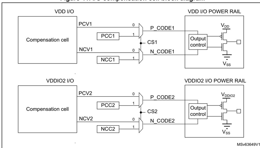
The diagram illustrates the internal structure of I/O compensation cells. It is divided into two horizontal sections. The top section is labeled 'VDD I/O' and the bottom section is labeled 'VDDIO2 I/O'. Each section contains a 'Compensation cell' block on the left. From the compensation cell, two lines emerge: 'PCV1' (or 'PCV2') and 'NCV1' (or 'NCV2'). These lines pass through 'PCC1' (or 'PCC2') and 'NCC1' (or 'NCC2') blocks respectively. The outputs of these blocks are 'P_CODE1' (or 'P_CODE2') and 'N_CODE1' (or 'N_CODE2'). These signals are connected to an 'Output control' block. The 'Output control' block is also connected to a power rail: 'VDD I/O POWER RAIL' (or 'VDDIO2 I/O POWER RAIL') and 'Vss'. Inside the 'Output control' block, there is a schematic of a CMOS inverter-like structure with 'VDD' (or 'VDDIO2') and 'Vss' labels. A common signal 'CS1' (or 'CS2') is connected to the 'Output control' block. The diagram is labeled 'MSv63649V1' in the bottom right corner.
13.2.2 SYSCFG TrustZone security and privilege
SYSCFG TrustZone security
When the TrustZone security is activated, the SYSCFG is able to secure registers from being modified by nonsecure accesses.
The TrustZone security is activated by the TZEN option bit in FLASH_OPTR.
A nonsecure read/write access to a secured register is RAZ/WI and generates an illegal access event. An illegal access interrupt is generated if the SYSCFG illegal access event is enabled in the GTZC.
Privileged/unprivileged mode
SYSCFG registers can be read and written by privileged and unprivileged accesses except the SYSCFG registers for CPU configuration: SYSCFG_CSLCKR, SYSCFG_FPUIMR, and SYSCFG_CNSLCKR registers, and the FPUSEC bit in SYSCFG_SECCFGR.
An unprivileged access to a privileged register is RAZ/WI.
The table below shows the register security overview.
Table 118. TrustZone security and privilege register accesses
| SYSCFG register | Read/write access | Privileged /unprivileged access | |
|---|---|---|---|
| TrustZone configuration (1) | TZEN = 1 | TZEN = 0 | Not applicable |
| SYSCFG_SECCFGR | Read: no restriction Write: secure access only nonsecure write is WI and generates an illegal access event. | RAZ/WI | Read: no restriction FPUSEC privileged write only Other bits write: no restriction |
| SYSCFG_CSLCKR | Read/Write: secure access only Nonsecure access is RAZ/WI and generates an illegal access event. | RAZ/WI | Privileged only Unprivileged: RAZ/WI |
| SYSCFG_FPUIMR | If FPUSEC = 1: Read/Write: secure access only Nonsecure access is RAZ/WI and generates an illegal access event. If FPUSEC = 0: Read/Write: no restriction | No restriction | Privileged only Unprivileged: RAZ/WI |
| SYSCFG_CNSLCKR | Read/write: no restriction | No restriction | Privileged only Unprivileged: RAZ/WI |
| SYSCFG_CFGR1 | Read/Write: secure access only for secure bits depending on peripheral security bits in GTZC Nonsecure access only for nonsecure bits, otherwise RAZ/WI | No restriction | No restriction |
| SYSCFG_CFGR2 | If CLASSBSEC = 1: Read/Write: secure access only Nonsecure access is RAZ/WI and generates an illegal access event. If CLASSBSEC = 0: Read/Write: no restriction | No restriction | No restriction |
| SYSCFG_CCCSR SYSCFG_CCVR SYSCFG_CCCR | If SYSCFGSEC = 1: Read/Write: secure access only Nonsecure access is RAZ/WI and generates an illegal access event If SYSCFGSEC = 0: Read/Write: no restriction | No restriction | No restriction |
| SYSCFG_RSSCMR | RAZ/WI if register access is not allowed (2) | RAZ/WI | No restriction |
1. TrustZone security is activated by the TZEN option bit in the FLASH_OPTER register.
2. Refer to register description for register access.
13.2.3 GPIO analog switches supply selection
Two bits from the SYSCFG_CFGR1 register are used to select the power supply of the I/O analog switches (used analog input signal paths): BOOSTEN and ANASWVDD.
They have to be initialized according to the voltage of the V DD and V DDA power supplies. When V DDA voltage is larger than 2.4 V, the I/O analog switches must be powered by V DDA .
When \( V_{DDA} \) voltage is lower than 2.4 V and \( V_{DD} \) is higher than 2.4 V, the I/O analog switches must be powered by \( V_{DD} \) . When both \( V_{DD} \) and \( V_{DDA} \) voltages are lower than 2.4 V, the I/O analog switches must be powered by the output of the \( V_{DD} \) booster. When I/O analog switches are supplied by \( V_{DDA} \) or \( V_{DD} \) booster, the ASV bit of the PWR_SVMCR register must be set.
Table 119. BOOSTEN and ANASWVDD set/reset
| \( V_{DD} \) | \( V_{DDA} \) | BOOSTEN | ANASWVDD |
|---|---|---|---|
| - | > 2.4 V | 0 | 0 |
| > 2.4 V | < 2.4 V | 1 | 1 |
| < 2.4 V | < 2.4 V | 1 | 0 |
13.3 SYSCFG registers
13.3.1 SYSCFG secure configuration register (SYSCFG_SECCFGR)
Address offset: 0x00
Reset value: 0x0000 0000
When the system is secure (TZEN = 1), this register provides write access security and can be written only when the access is secure. This register can be globally write-protected. Each bit can be individually write-protected. A nonsecure write access is WI and generates an illegal access event. There are no read restrictions.
When the system is not secure (TZEN = 0), this register is RAZ/WI.
This register can be read and written by privileged and unprivileged access, except for FPUSEC that can be written only with privileged access.
| 31 | 30 | 29 | 28 | 27 | 26 | 25 | 24 | 23 | 22 | 21 | 20 | 19 | 18 | 17 | 16 |
|---|---|---|---|---|---|---|---|---|---|---|---|---|---|---|---|
| Res. | Res. | Res. | Res. | Res. | Res. | Res. | Res. | Res. | Res. | Res. | Res. | Res. | Res. | Res. | Res. |
| 15 | 14 | 13 | 12 | 11 | 10 | 9 | 8 | 7 | 6 | 5 | 4 | 3 | 2 | 1 | 0 |
| Res. | Res. | Res. | Res. | Res. | Res. | Res. | Res. | Res. | Res. | Res. | Res. | FPUSEC | Res. | CLASSBSEC | SYSCFGSEC |
| rw | rw | rw |
Bits 31:4 Reserved, must be kept at reset value.
Bit 3 FPUSEC : FPU security
0: SYSCFG_FPUIMR can be read and written by secure and nonsecure access.
1: SYSCFG_FPUIMR can be read and written by secure access only.
Bit 2 Reserved, must be kept at reset value.
Bit 1 CLASSBSEC : Class B security
0: SYSCFG_CFGR2 can be read and written by secure and nonsecure access.
1: SYSCFG_CFGR2 can be read and written by secure access only.
Bit 0 SYSCFGSEC : Security of SYSCFG clock control, memory erase status, and compensation cell registers
0: SYSCFG configuration clock in RCC registers and SYSCFG_CCCSR, SYSCFG_CCVR, and SYSCFG_CCCR can be read and written by secure and nonsecure access.
1: SYSCFG configuration clock in RCC registers and SYSCFG_CCCSR, SYSCFG_CCVR, and SYSCFG_CCCR can be read and written by secure access only.
13.3.2 SYSCFG configuration register 1 (SYSCFG_CFGR1)
Address offset: 0x04
Reset value: 0x0000 0000
When the system is secure (TZEN = 1), this register can be a mix of secure and nonsecure bits depending on the ADC and the TSC security configuration bit in GTZC peripheral and GPIO security bits. A nonsecure read/write access on secured bits is RAZ/WI.
When the system is not secure (TZEN = 0), there is no access restriction.
This register can be read and written by privileged and unprivileged access.
| 31 | 30 | 29 | 28 | 27 | 26 | 25 | 24 | 23 | 22 | 21 | 20 | 19 | 18 | 17 | 16 |
|---|---|---|---|---|---|---|---|---|---|---|---|---|---|---|---|
| Res. | Res. | Res. | Res. | Res. | Res. | TSC_G 2_IO3_ COMP | TSC_G 2_IO1_ COMP | Res. | Res. | Res. | Res. | PB9_F MP | PB8_F MP | PB7_F MP | PB6_F MP |
| rw | rw | rw | rw | rw | rw | ||||||||||
| 15 | 14 | 13 | 12 | 11 | 10 | 9 | 8 | 7 | 6 | 5 | 4 | 3 | 2 | 1 | 0 |
| Res. | Res. | Res. | Res. | Res. | Res. | ANAS WVDD | BOOST EN | IR_MOD[1:0] | IR_PO L | Res. | Res. | Res. | Res. | Res. | |
| rw | rw | rw | rw | rw |
Bits 31:26 Reserved, must be kept at reset value.
Bit 25 TSC_G2_IO3_COMP : Comparator mode for G2_IO3 on PB6
This bit can be read and written only with secure access if TSC is secure in GTZC.
0: Normal mode: TSC_G2_IO3 detection is done using PB6 V IH I/O threshold. PB6 is configured through GPIOB registers.
1: Comparator mode: TSC_G2_IO3 detection is done using COMP2_INM threshold. When TSC_G2_IO3 is selected as PB6 alternate function, TSC_G2_IO3 is connected to COMP2_OUT, PB6 is forced in analog mode, and PB6 can be connected to COMP2_INP2 (configuration must also be done in COMP block).
Note: This bit is only available on STM32U3B5/3C5.
Bit 24 TSC_G2_IO1_COMP : Comparator mode for G2_IO1 on PB4
This bit can be read and written only with secure access if TSC is secure in GTZC.
0: Normal mode: TSC_G2_IO1 detection is done using PB4 V IH I/O threshold. PB4 is configured through GPIOB registers.
1: Comparator mode: TSC_G2_IO1 detection is done using COMP2_INM threshold. When TSC_G2_IO1 is selected as PB4 alternate function, TSC_G2_IO1 is connected to COMP2_OUT, PB4 is forced in analog mode, and PB4 can be connected to COMP2_INP2 (configuration must also be done in COMP block).
Note: This bit is only available on STM32U3B5/3C5.
Bits 23:20 Reserved, must be kept at reset value.
Bits 19:16 PBi_FMP : Fast-mode Plus driving capability activation on PBi (i = 9 to 6)
This bit can be read and written only with secure access if PB9 is secure in GPIOB. This bit enables the Fm+ driving mode for PBi when PBi is not used by the I2C peripheral. This can be used to drive a LED for instance.
0: PBi pin operates in standard mode.
1: Fm+ mode is enabled on PBi pin and the speed control is bypassed.
Bits 15:10 Reserved, must be kept at reset value.
Bit 9 ANASWVDD : GPIO analog switch control voltage selection
This bit can be read and written only with secure access if ADC1 or ADC2 is secure in GTZC.
0: If booster is OFF: I/O analog switches are supplied by V DDA if ASV = 1 in PWR_SVMCR, or by V DD if ASV = 0.
If booster is ON: I/O analog switches are supplied by booster.
1: I/O analog switches are supplied by V DD .
Note: Refer to Table 119: BOOSTEN and ANASWVDD set/reset
Bit 8 BOOSTEN : I/O analog switch voltage booster enable
This bit is only effective when ASV = 1 in PWR_SVMR, and ANASWVDD = 0.
This bit can be read and written only with secure access if ADC1 or ADC2 is secure in GTZC.
0: I/O analog switches are supplied by V DDA voltage.
1: I/O analog switches are supplied by a dedicated voltage booster (supplied by V DD ).
Note: Refer to Table 119: BOOSTEN and ANASWVDD set/reset
Bits 7:6 IR_MOD[1:0] : IR modulation envelope signal selection
This bitfield can be read and written only with secure access if TIM17 is secure in GTZC.
It selects the signal for IR modulation envelope.
00: TIM16
01: USART1
10: UART4
11: Reserved
Note: Refer to Table 119: BOOSTEN and ANASWVDD set/reset
Bit 5 IR_POL : IR output polarity selection
This bit can be read and written only with secure access if TIM17 is secure in GTZC.
0: Output of IRTIM (IR_OUT) is not inverted.
1: Output of IRTIM (IR_OUT) is inverted.
Note: Refer to Table 119: BOOSTEN and ANASWVDD set/reset
Bits 4:0 Reserved, must be kept at reset value.
13.3.3 SYSCFG FPU interrupt mask register (SYSCFG_FPUIMR)
Address offset: 0x08
Reset value: 0x0000 001F
When the system is secure (TZEN = 1), this register can be protected against nonsecure access by setting the FPUSEC bit in the SYSCFG_SECCFGR register: a nonsecure read/write access is RAZ/WI and generates an illegal access event.
When the system is not secure (TZEN = 0), there is no access restriction. This register can be read and written by privileged access only. Unprivileged access is RAZ/WI.
| 31 | 30 | 29 | 28 | 27 | 26 | 25 | 24 | 23 | 22 | 21 | 20 | 19 | 18 | 17 | 16 |
|---|---|---|---|---|---|---|---|---|---|---|---|---|---|---|---|
| Res. | Res. | Res. | Res. | Res. | Res. | Res. | Res. | Res. | Res. | Res. | Res. | Res. | Res. | Res. | Res. |
| 15 | 14 | 13 | 12 | 11 | 10 | 9 | 8 | 7 | 6 | 5 | 4 | 3 | 2 | 1 | 0 |
| Res. | Res. | Res. | Res. | Res. | Res. | Res. | Res. | Res. | Res. | FPU_IX IE | FPU_I DIE | FPU_O FIE | FPU_U FIE | FPU_D ZIE | FPU_I OIE |
| rw | rw | rw | rw | rw | rw |
Bits 31:6 Reserved, must be kept at reset value.
Bit 5 FPU_IXIE : Floating point unit interrupt enable bit - inexact
FPU inexact interrupt enable bit (interrupt disable at reset)
0: Interrupt disabled
1: Interrupt enabled
Bit 4 FPU_IDIE : Floating point unit interrupt enable bit - input denormal
FPU denormal interrupt enable bit
0: Interrupt disabled
1: Interrupt enabled
Bit 3 FPU_OFIE : Floating point unit interrupt enable bit - overflow
FPU overflow interrupt enable bit
0: Interrupt disabled
1: Interrupt enabled
Bit 2 FPU_UFIE : Floating point unit interrupt enable bit - underflow
FPU underflow interrupt enable bit
0: Interrupt disabled
1: Interrupt enabled
Bit 1 FPU_DZIE : Floating point unit interrupt enable bit - divide-by-zero
FPU divide-by-zero interrupt enable bit
0: Interrupt disabled
1: Interrupt enabled
Bit 0 FPU_IOIE : Floating point unit interrupt enable bit - invalid operation
FPU invalid operation interrupt enable bit
0: Interrupt disabled
1: Interrupt enabled
13.3.4 SYSCFG CPU nonsecure lock register (SYSCFG_CNSLCKR)
Address offset: 0x0C
Reset value: 0x0000 0000
This register is used to lock the configuration of nonsecure MPU and VTOR_NS registers. This register can be read and written by privileged access only. Unprivileged access is RAZ/WI.
| 31 | 30 | 29 | 28 | 27 | 26 | 25 | 24 | 23 | 22 | 21 | 20 | 19 | 18 | 17 | 16 |
|---|---|---|---|---|---|---|---|---|---|---|---|---|---|---|---|
| Res. | Res. | Res. | Res. | Res. | Res. | Res. | Res. | Res. | Res. | Res. | Res. | Res. | Res. | Res. | Res. |
| 15 | 14 | 13 | 12 | 11 | 10 | 9 | 8 | 7 | 6 | 5 | 4 | 3 | 2 | 1 | 0 |
| Res. | Res. | Res. | Res. | Res. | Res. | Res. | Res. | Res. | Res. | Res. | Res. | Res. | Res. | LOCKN SMPU | LOCKN SVTOR |
| rs | rs |
Bits 31:2 Reserved, must be kept at reset value.
Bit 1 LOCKNSMPU : Nonsecure MPU registers lock
This bit is set by software and cleared only by a system reset. When set, this bit disables write access to nonsecure MPU_CTRL_NS, MPU_RNR_NS, and MPU_RBAR_NS registers.
0: Nonsecure MPU register write enabled
1: Nonsecure MPU register write disabled
Bit 0 LOCKNSVTOR : VTOR_NS register lock
This bit is set by software and cleared only by a system reset.
0: VTOR_NS register write enabled
1: VTOR_NS register write disabled
13.3.5 SYSCFG CPU secure lock register (SYSCFG_CSLCKR)
Address offset: 0x10
Reset value: 0x0000 0000
This register is used to lock the configuration of PRIS and BFHFNMINs in AIRCR register, SAU, secure MPU, and VTOR_S registers.
When the system is secure (TZEN = 1), this register can be written only when the access is secure. A nonsecure read/write access is RAZ/WI and generates an illegal access event.
When the system is not secure (TZEN = 0), this register is RAZ/WI. This register can be read and written by privileged access only. Unprivileged access is RAZ/WI.
| 31 | 30 | 29 | 28 | 27 | 26 | 25 | 24 | 23 | 22 | 21 | 20 | 19 | 18 | 17 | 16 |
|---|---|---|---|---|---|---|---|---|---|---|---|---|---|---|---|
| Res. | Res. | Res. | Res. | Res. | Res. | Res. | Res. | Res. | Res. | Res. | Res. | Res. | Res. | Res. | Res. |
| 15 | 14 | 13 | 12 | 11 | 10 | 9 | 8 | 7 | 6 | 5 | 4 | 3 | 2 | 1 | 0 |
| Res. | Res. | Res. | Res. | Res. | Res. | Res. | Res. | Res. | Res. | Res. | Res. | Res. | LOCKSAU | LOCKSMPU | LOCKSVTAIR CR |
| rs | rs | rs |
Bits 31:3 Reserved, must be kept at reset value.
Bit 2 LOCKSAU : SAU register lock
This bit is set by software and cleared only by a system reset. When set, this bit disables write access to SAU_CTRL, SAU_RNR, SAU_RBAR, and SAU_RLAR registers.
0: SAU register write enabled
1: SAU register write disabled
Bit 1 LOCKSMPU : Secure MPU registers lock
This bit is set by software and cleared only by a system reset. When set, this bit disables write access to secure MPU_CTRL, MPU_RNR, and MPU_RBAR registers.
0: Secure MPU register writes enabled
1: Secure MPU register writes disabled
Bit 0 LOCKSVTAIRCR : VTOR_S register and AIRCR register bits lock
This bit is set by software and cleared only by a system reset. When set, this bit disables write access to VTOR_S register, PRIS and BFHFNMINS bits in the AIRCR register.
0: VTOR_S register PRIS and BFHFNMINS bits in AIRCR register write enabled
1: VTOR_S register PRIS and BFHFNMINS bits in AIRCR register write disabled
13.3.6 SYSCFG configuration register 2 (SYSCFG_CFGR2)
Address offset: 0x14
Reset value: 0x0000 0000
When the system is secure (TZEN = 1), this register can be protected against nonsecure access by setting the CLASSBSEC bit in the SYSCFG_SECCFGR register.
When CLASSBSEC bit is set, only secure access is allowed: nonsecure read/write access is RAZ/WI and generates an illegal access event.
When the system is not secure (TZEN = 0), there is no access restriction. This register can be read and written by privileged and unprivileged access.
| 31 | 30 | 29 | 28 | 27 | 26 | 25 | 24 | 23 | 22 | 21 | 20 | 19 | 18 | 17 | 16 |
|---|---|---|---|---|---|---|---|---|---|---|---|---|---|---|---|
| Res. | Res. | Res. | Res. | Res. | Res. | Res. | Res. | Res. | Res. | Res. | Res. | Res. | Res. | Res. | Res. |
| 15 | 14 | 13 | 12 | 11 | 10 | 9 | 8 | 7 | 6 | 5 | 4 | 3 | 2 | 1 | 0 |
| Res. | Res. | Res. | Res. | Res. | Res. | Res. | Res. | Res. | Res. | Res. | Res. | ECCL | PVDL | SPL | CLL |
| rs | rs | rs | rs |
Bits 31:4 Reserved, must be kept at reset value.
Bit 3 ECCL : ECC lock
This bit is set by software and cleared only by a system reset. It can be used to enable and lock the FLASH ECC double error signal connection to the TIM1/8/15/16/17 break input.
0: ECC double error disconnected from TIM1/8/15/16/17 break input
1: ECC double error connected to TIM1/8/15/16/17 break input
Note: TIM8 is only available on STM32U3B5/3C5.
Bit 2 PVDL : PVD lock enable bitThis bit is set by software and cleared only by a system reset. It can be used to enable and lock the PVD connection to TIM1/8/15/16/17 break input, as well as the PVDE and PVDLS[2:0] in the PWR register.
0: PVD interrupt disconnected from TIM1/8/15/16/17 break input. PVDE and PVDLS[2:0] bits can be programmed by the application.
1: PVD interrupt connected to TIM1/8/15/16/17 break input. PVDE and PVDLS[2:0] bits are read only.
Note: TIM8 is only available on STM32U3B5/3C5.
Bit 1 SPL : SRAM2 parity bitThis bit is set by the software and cleared only by a system reset. It can be used to enable and lock the SRAM2 parity error signal connection to TIM1/8/15/16/17 break inputs.
0: SRAM double error disconnected from TIM1/8/15/16/17 break inputs
1: SRAM double error connected to TIM1/8/15/16/17 break inputs
Note: TIM8 is only available on STM32U3B5/3C5.
Bit 0 CLL : Cortex-M33 LOCKUP (HardFault) output enableThis bit is set by the software and cleared only by a system reset. It can be used to enable and lock the connection of Cortex-M33 LOCKUP (HardFault) output to TIM1/15/16/17 break input.
0: Cortex-M33 LOCKUP output disconnected from TIM1/8/15/16/17 break inputs
1: Cortex-M33 LOCKUP output connected to TIM1/8/15/16/17 break inputs
Note: TIM8 is only available on STM32U3B5/3C5.
13.3.7 SYSCFG compensation cell control/status register (SYSCFG_CCCSR)
Address offset: 0x1C
Reset value: 0x0000 000A
When the system is secure (TZEN = 1), this register can be protected against nonsecure access by setting the SYSCFGSEC bit in SYSCFG_SECCFGR register. When the SYSCFGSEC bit is set, only secure access is allowed: nonsecure read/write access is RAZ/WI and generates an illegal access event.
When the system is not secure (TZEN = 0), there is no access restriction. This register can be read and written by privileged and unprivileged access.
| 31 | 30 | 29 | 28 | 27 | 26 | 25 | 24 | 23 | 22 | 21 | 20 | 19 | 18 | 17 | 16 |
|---|---|---|---|---|---|---|---|---|---|---|---|---|---|---|---|
| Res. | Res. | Res. | Res. | Res. | Res. | Res. | Res. | Res. | Res. | Res. | Res. | Res. | Res. | Res. | Res. |
| 15 | 14 | 13 | 12 | 11 | 10 | 9 | 8 | 7 | 6 | 5 | 4 | 3 | 2 | 1 | 0 |
| Res. | Res. | Res. | Res. | Res. | Res. | RDY2 | RDY1 | Res. | Res. | Res. | Res. | CS2 | EN2 | CS1 | EN1 |
| r | r | rw | rw | rw | rw |
Bits 31:10 Reserved, must be kept at reset value.
Bit 9 RDY2 : VDDIO2 I/O compensation cell ready flag
This bit provides the compensation cell status of the I/Os supplied by \( V_{DDIO2} \) .
0: VDDIO2 I/O compensation cell not ready
1: VDDIO2 I/O compensation cell ready
Note: The HSI clock is required for the compensation cell to work properly. The compensation cell ready bit (RDY2) is not set if the HSI clock is not enabled.
Note: This feature is not available on STM32U356/366 series.
Bit 8 RDY1 : VDD I/O compensation cell ready flag
This bit provides the compensation cell status of the I/Os supplied by \( V_{DD} \) .
0: VDD I/O compensation cell not ready
1: VDD I/O compensation cell ready
Note: The HSI clock is required for the compensation cell to work properly. The compensation cell ready bit (RDY1) is not set if the HSI clock is not enabled.
Bits 7:4 Reserved, must be kept at reset value.
Bit 3 CS2 : VDDIO2 I/O code selection
This bit selects the code to be applied for the compensation cell of the I/Os supplied by \( V_{DDIO2} \) .
0: VDDIO2 I/O code from the cell (available in SYSCFG_CCVR)
1: VDDIO2 I/O code from SYSCFG_CCCR
Note: This feature is not available on STM32U356/366 series.
Bit 2 EN2 : VDDIO2 I/O compensation cell enable
This bit enables the compensation cell of the I/Os supplied by \( V_{DDIO2} \) .
0: VDDIO2 I/O compensation cell disabled
1: VDDIO2 I/O compensation cell enabled
Note: This feature is not available on STM32U356/366 series.
Bit 1 CS1 : VDD I/O code selection
This bit selects the code to be applied for the compensation cell of the I/Os supplied by \( V_{DD} \) .
0: VDD I/O code from the cell (available in the SYSCFG_CCVR)
1: VDD I/O code from the SYSCFG compensation cell code register (SYSCFG_CCCR)
Bit 0 EN1 : VDD I/O compensation cell enable
This bit enables the compensation cell of the I/Os supplied by \( V_{DD} \) .
0: VDD I/O compensation cell disabled
1: VDD I/O compensation cell enabled
13.3.8 SYSCFG compensation cell value register (SYSCFG_CCVR)
Address offset: 0x20
Reset value: 0x0000 0000
When the system is secure (TZEN = 1), this register can be protected against nonsecure access by setting the SYSCFGSEC bit in the SYSCFG_SECCFGR register. When the SYSCFGSEC bit is set, only secure access is allowed: nonsecure read/write access is RAZ/WI and generates an illegal access event.
When the system is not secure (TZEN = 0), there is no access restriction. This register can be read and written by privileged and unprivileged access.
| 31 | 30 | 29 | 28 | 27 | 26 | 25 | 24 | 23 | 22 | 21 | 20 | 19 | 18 | 17 | 16 |
|---|---|---|---|---|---|---|---|---|---|---|---|---|---|---|---|
| Res. | Res. | Res. | Res. | Res. | Res. | Res. | Res. | Res. | Res. | Res. | Res. | Res. | Res. | Res. | Res. |
| 15 | 14 | 13 | 12 | 11 | 10 | 9 | 8 | 7 | 6 | 5 | 4 | 3 | 2 | 1 | 0 |
| PCV2[3:0] | NCV2[3:0] | PCV1[3:0] | NCV1[3:0] | ||||||||||||
| r | r | r | r | r | r | r | r | r | r | r | r | r | r | r | r |
Bits 31:16 Reserved, must be kept at reset value.
Bits 15:12 PCV2[3:0] : PMOS compensation value of the I/Os supplied by \( V_{DDIO2} \)
This value is provided by the cell and can be used by the CPU to compute an I/O compensation cell code for PMOS transistors. This code is applied to the I/O compensation cell when CS2 bit in SYSCFG_CCCSR is reset.
Bits 11:8 NCV2[3:0] : NMOS compensation value of the I/Os supplied by \( V_{DDIO2} \)
This value is provided by the cell and can be used by the CPU to compute an I/O compensation cell code for NMOS transistors. This code is applied to the I/O compensation cell when CS2 bit in SYSCFG_CCCSR is reset.
Bits 7:4 PCV1[3:0] : PMOS compensation value of the I/Os supplied by \( V_{DD} \)
This value is provided by the cell and can be used by the CPU to compute an I/O compensation cell code for PMOS transistors. This code is applied to the I/O compensation cell when CS1 bit in SYSCFG_CCCSR is reset.
Bits 3:0 NCV1[3:0] : NMOS compensation value of the I/Os supplied by \( V_{DD} \)
This value is provided by the cell and can be used by the CPU to compute an I/O compensation cell code for NMOS transistors. This code is applied to the I/O compensation cell when CS1 bit in SYSCFG_CCCSR is reset.
13.3.9 SYSCFG compensation cell code register (SYSCFG_CCCR)
Address offset: 0x24
Reset value: 0x0000 7878
When the system is secure (TZEN = 1), this register can be protected against nonsecure access by setting the SYSCFGSEC bit in the SYSCFG_SECCFGR register. When SYSCFGSEC bit is set, only secure access is allowed: nonsecure read/write access is RAZ/WI and generates an illegal access event.
When the system is not secure (TZEN = 0), there is no access restriction. This register can be read and written by privileged and unprivileged access.
| 31 | 30 | 29 | 28 | 27 | 26 | 25 | 24 | 23 | 22 | 21 | 20 | 19 | 18 | 17 | 16 |
|---|---|---|---|---|---|---|---|---|---|---|---|---|---|---|---|
| Res. | Res. | Res. | Res. | Res. | Res. | Res. | Res. | Res. | Res. | Res. | Res. | Res. | Res. | Res. | Res. |
| 15 | 14 | 13 | 12 | 11 | 10 | 9 | 8 | 7 | 6 | 5 | 4 | 3 | 2 | 1 | 0 |
| PCC2[3:0] | NCC2[3:0] | PCC1[3:0] | NCC1[3:0] | ||||||||||||
| rw | rw | rw | rw | rw | rw | rw | rw | rw | rw | rw | rw | rw | rw | rw | rw |
Bits 31:16 Reserved, must be kept at reset value.
Bits 15:12 PCC2[3:0] : PMOS compensation code of the I/Os supplied by V DDIO2
These bits are written by software to define an I/O compensation cell code for PMOS transistors. This code is applied to the I/O compensation cell when CS2 bit is set in SYSCFG_CCCSR.
Bits 11:8 NCC2[3:0] : NMOS compensation code of the I/Os supplied by V DDIO2
These bits are written by software to define an I/O compensation cell code for NMOS transistors. This code is applied to the I/O compensation cell when CS2 bit is set in SYSCFG_CCCSR.
Bits 7:4 PCC1[3:0] : PMOS compensation code of the I/Os supplied by V DD
These bits are written by software to define an I/O compensation cell code for PMOS transistors. This code is applied to the I/O compensation cell when CS1 bit is set in SYSCFG_CCCSR.
Bits 3:0 NCC1[3:0] : NMOS compensation code of the I/Os supplied by V DD
These bits are written by software to define an I/O compensation cell code for NMOS transistors. This code is applied to the I/O compensation cell when CS1 bit is set in SYSCFG_CCCSR.
13.3.10 SYSCFG RSS command register (SYSCFG_RSSCMDR)
Address offset: 0x2C
Power-on reset value: 0x0000 0000
System reset value: 0xUUUU UUUU (not affected)
When the system is secure (TZEN = 1), this register can be read and written only when the APB access is secure. Otherwise it is RAZ/WI.
When the system is not secure (TZEN = 0), this register is RAZ/WI. This register can be read and written by privileged and unprivileged access.
| 31 | 30 | 29 | 28 | 27 | 26 | 25 | 24 | 23 | 22 | 21 | 20 | 19 | 18 | 17 | 16 |
|---|---|---|---|---|---|---|---|---|---|---|---|---|---|---|---|
| Res. | Res. | Res. | Res. | Res. | Res. | Res. | Res. | Res. | Res. | Res. | Res. | Res. | Res. | Res. | Res. |
| 15 | 14 | 13 | 12 | 11 | 10 | 9 | 8 | 7 | 6 | 5 | 4 | 3 | 2 | 1 | 0 |
| RSSCMD[15:0] | |||||||||||||||
| rw | rw | rw | rw | rw | rw | rw | rw | rw | rw | rw | rw | rw | rw | rw | rw |
Bits 31:16 Reserved, must be kept at reset value.
Bits 15:0
RSSCMD[15:0]
: RSS commands
This bitfield defines a command to be executed by the RSS.
13.3.11 SYSCFG register map
Table 120. SYSCFG register map and reset values
| Offset | Register name | 31 | 30 | 29 | 28 | 27 | 26 | 25 | 24 | 23 | 22 | 21 | 20 | 19 | 18 | 17 | 16 | 15 | 14 | 13 | 12 | 11 | 10 | 9 | 8 | 7 | 6 | 5 | 4 | 3 | 2 | 1 | 0 |
|---|---|---|---|---|---|---|---|---|---|---|---|---|---|---|---|---|---|---|---|---|---|---|---|---|---|---|---|---|---|---|---|---|---|
| 0x00 | SYSCFG_SECCFGR | Res. | Res. | Res. | Res. | Res. | Res. | Res. | Res. | Res. | Res. | Res. | Res. | Res. | Res. | Res. | Res. | Res. | Res. | Res. | Res. | Res. | Res. | Res. | Res. | Res. | Res. | Res. | Res. | FPUSECC | Res. | CLASSBSEC | SYSCFGSEC |
| Reset value | 0 | 0 | 0 | ||||||||||||||||||||||||||||||
| 0x04 | SYSCFG_CFGR1 | Res. | Res. | Res. | Res. | Res. | TSC_G2_IO3_COMP | TSC_G2_IO2_COMP | Res. | Res. | Res. | Res. | Res. | PB9_FMP | PB8_FMP | PB7_FMP | PB6_FMP | Res. | Res. | Res. | Res. | Res. | Res. | ANASWVDD | BOOSTEN | IR_MOD[1:0] | IR_POL | Res. | Res. | Res. | Res. | Res. | |
| Reset value | 0 | 0 | 0 | 0 | 0 | 0 | 0 | 0 | 0 | 0 | 0 | ||||||||||||||||||||||
| 0x08 | SYSCFG_FPUIMR | Res. | Res. | Res. | Res. | Res. | Res. | Res. | Res. | Res. | Res. | Res. | Res. | Res. | Res. | Res. | Res. | Res. | Res. | Res. | Res. | Res. | Res. | Res. | Res. | Res. | Res. | FPU_IXIE | FPU_IDIE | FPU_OFIE | FPU_UFIE | FPU_DZIE | FPU_IOIE |
| Reset value | 0 | 1 | 1 | 1 | 1 | 1 | |||||||||||||||||||||||||||
| 0x0C | SYSCFG_CNSLCKR | Res. | Res. | Res. | Res. | Res. | Res. | Res. | Res. | Res. | Res. | Res. | Res. | Res. | Res. | Res. | Res. | Res. | Res. | Res. | Res. | Res. | Res. | Res. | Res. | Res. | Res. | Res. | Res. | Res. | Res. | LOCKNSMPU | LOCKNSVTOR |
| Reset value | 0 | 0 | |||||||||||||||||||||||||||||||
Table 120. SYSCFG register map and reset values (continued)
| Offset | Register name | 31 | 30 | 29 | 28 | 27 | 26 | 25 | 24 | 23 | 22 | 21 | 20 | 19 | 18 | 17 | 16 | 15 | 14 | 13 | 12 | 11 | 10 | 9 | 8 | 7 | 6 | 5 | 4 | 3 | 2 | 1 | 0 |
|---|---|---|---|---|---|---|---|---|---|---|---|---|---|---|---|---|---|---|---|---|---|---|---|---|---|---|---|---|---|---|---|---|---|
| 0x10 | SYSCFG_CSLCKR | Res. | Res. | Res. | Res. | Res. | Res. | Res. | Res. | Res. | Res. | Res. | Res. | Res. | Res. | Res. | Res. | Res. | Res. | Res. | Res. | Res. | Res. | Res. | Res. | Res. | Res. | Res. | Res. | Res. | LOCKSAU | LOCKSMPU | LOCKSVTAIRCR |
| Reset value | 0 | 0 | 0 | ||||||||||||||||||||||||||||||
| 0x14 | SYSCFG_CFGR2 | Res. | Res. | Res. | Res. | Res. | Res. | Res. | Res. | Res. | Res. | Res. | Res. | Res. | Res. | Res. | Res. | Res. | Res. | Res. | Res. | Res. | Res. | Res. | Res. | Res. | Res. | Res. | ECCL | PVDL | SPL | CLL | |
| Reset value | 0 | 0 | 0 | 0 | |||||||||||||||||||||||||||||
| 0x18 | Reserved | Reserved | |||||||||||||||||||||||||||||||
| 0x1C | SYSCFG_CCCSR | Res. | Res. | Res. | Res. | Res. | Res. | Res. | Res. | Res. | Res. | Res. | Res. | Res. | Res. | Res. | Res. | Res. | Res. | Res. | Res. | Res. | RDY2 | RDY1 | Res. | Res. | Res. | Res. | Res. | CS2 | EN2 | CS1 | EN1 |
| Reset value | 0 | 0 | 1 | 0 | 1 | 0 | |||||||||||||||||||||||||||
| 0x20 | SYSCFG_CCVR | Res. | Res. | Res. | Res. | Res. | Res. | Res. | Res. | Res. | Res. | Res. | Res. | Res. | Res. | Res. | Res. | PCV2[3:0] | NCV2[3:0] | PCV1[3:0] | NCV1[3:0] | ||||||||||||
| Reset value | 0 | 0 | 0 | 0 | 0 | 0 | 0 | 0 | 0 | 0 | 0 | 0 | 0 | 0 | 0 | 0 | |||||||||||||||||
| 0x24 | SYSCFG_CCCR | Res. | Res. | Res. | Res. | Res. | Res. | Res. | Res. | Res. | Res. | Res. | Res. | Res. | Res. | Res. | Res. | PCC2[3:0] | NCC2[3:0] | PCC1[3:0] | NCC1[3:0] | ||||||||||||
| Reset value | 0 | 1 | 1 | 1 | 0 | 0 | 0 | 0 | 1 | 1 | 1 | 1 | 0 | 0 | 0 | 0 | |||||||||||||||||
| 0x28 | Reserved | Reserved | |||||||||||||||||||||||||||||||
| 0x2C | SYSCFG_RSSCMDR | Res. | Res. | Res. | Res. | Res. | Res. | Res. | Res. | Res. | Res. | Res. | Res. | Res. | Res. | Res. | Res. | RSSCMD[15:0] | |||||||||||||||
| Power-on reset value | 0 | 0 | 0 | 0 | 0 | 0 | 0 | 0 | 0 | 0 | 0 | 0 | 0 | 0 | 0 | 0 | |||||||||||||||||
Refer to Section 2.3 for the register boundary addresses.
