11. Clock recovery system (CRS)
11.1 CRS introduction
The clock recovery system (CRS) is an advanced digital controller acting on the internal fine-granularity trimmable RC oscillator HSI48. The CRS provides powerful means to evaluate the oscillator output frequency, based on comparison with a selectable synchronization signal. The CRS can perform automatic trimming adjustments based on the measured frequency error value, while keeping the possibility of a manual trimming.
The CRS is ideally suited to provide a precise clock to the USB peripheral. In this case, the synchronization signal can be derived from the start-of-frame (SOF) packet signalization on the USB bus, sent by a USB host at 1 ms intervals.
The synchronization signal can also be derived from alternative synchronization or generated by the user software.
11.2 CRS main features
- • Selectable synchronization source with programmable prescaler and polarity (see Section 11.4.2: CRS internal signals )
- • Possibility to generate synchronization pulses by software
- • Automatic oscillator trimming capability with no need of CPU action
- • Manual control option for faster startup convergence
- • 16-bit frequency error counter with automatic error value capture and reload
- • Programmable limit for automatic frequency error value evaluation and status reporting
- • Maskable interrupts/events:
- – Expected synchronization (ESYNC)
- – Synchronization OK (SYNCOK)
- – Synchronization warning (SYNCWARN)
- – Synchronization or trimming error (ERR)
11.3 CRS implementation
Table 108. CRS features
| Feature | CRS |
|---|---|
| TRIM width | 7 bits |
11.4 CRS functional description
11.4.1 CRS block diagram
Figure 34. CRS block diagram
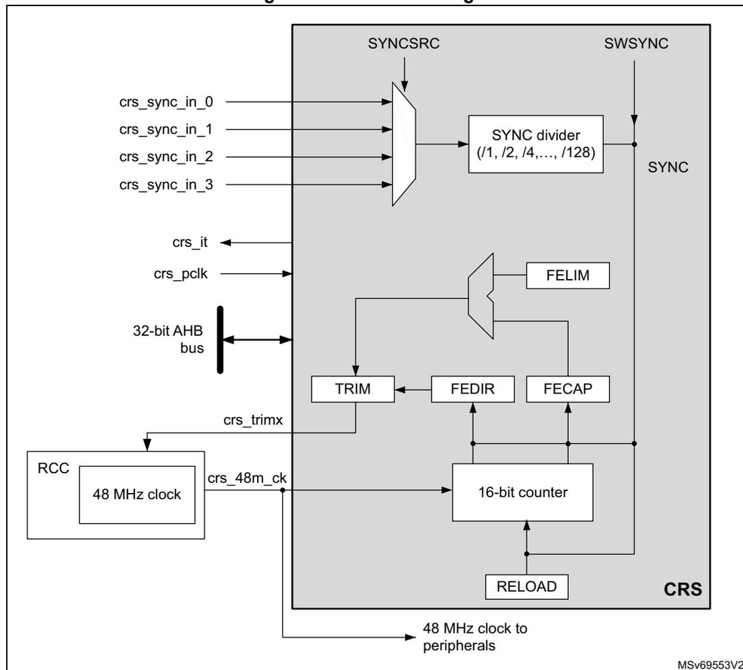
The block diagram illustrates the internal architecture of the Clock Recovery System (CRS). On the left, external signals are shown:
crs_sync_in_0
,
crs_sync_in_1
,
crs_sync_in_2
, and
crs_sync_in_3
(inputs to a multiplexer);
crs_it
(output from the CRS block);
crs_pclk
(input to the CRS block); a 32-bit AHB bus (bidirectional connection to the CRS block);
crs_trimx
(output from the TRIM block to the RCC); and
crs_48m_ck
(input from the RCC 48 MHz clock to the 16-bit counter). The RCC block contains a 48 MHz clock source. The CRS block itself contains several internal components: a multiplexer for
SYNC
selection (controlled by
SYNCSRC
); a
SYNC divider
(
\(
/1, /2, /4, \dots, /128
\)
) that generates the
SYNC
signal (controlled by
SWSYNC
); a
FELIM
block; a
TRIM
block; a
FEDIR
block; a
FECAP
block; a
16-bit counter
(controlled by
RELOAD
); and a
RELOAD
block. The 16-bit counter outputs a
48 MHz clock to peripherals
.
11.4.2 CRS internal signals
Below the list of CRS internal signals.
Table 109. CRS internal input/output signals
| Internal signal name | Signal type | Description |
|---|---|---|
crs_it | Digital output | CRS interrupt |
crs_pclk | Digital input | AHB bus clock |
crs_48m_ck | Digital input | HSI48 48 MHz clock |
crs_trim[0:6] | Digital output | HSI48 oscillator smooth trimming value |
Table 109. CRS internal input/output signals (continued)
| Internal signal name | Signal type | Description |
|---|---|---|
| crs_sync_in_0 | Digital input | SYNC signal source |
| crs_sync_in_1 | ||
| crs_sync_in_2 | ||
| crs_sync_in_3 |
Table 110. CRS interconnection
| Internal signal name | Source |
|---|---|
| crs_sync_in_0 | CRS_SYNC |
| crs_sync_in_1 | LSE clock |
| crs_sync_in_2 | USB SOF |
| crs_sync_in_3 | Reserved |
11.4.3 Synchronization input
The CRS synchronization source (crs_sync_in_x) can be selected through SYNC SRC[1:0] bitfield of CRS_CFGR register (refer to Section 11.4.2: CRS internal signals for the possible sources). For a better robustness of the crs_sync_in_x input, a simple digital filter (2 out of 3 majority votes, sampled by the 48 MHz clock) is implemented to filter out glitches. In addition, the source signal has a configurable polarity (selected through SYNCPOL bit of CRS_CFGR). The signal can then be divided by a programmable binary prescaler to obtain a synchronization signal in a suitable frequency range (usually around 1 kHz).
For more information on the CRS synchronization source configuration, refer to CRS_CFGR register.
It is also possible to generate a synchronization event by software, by setting the SWSYNC bit in the CRS_CR register.
For more information on the CRS synchronization source configuration, refer to CRS configuration register (CRS_CFGR) .
It is also possible to generate a synchronization event by software, by setting the SWSYNC bit in the CRS_CR register.
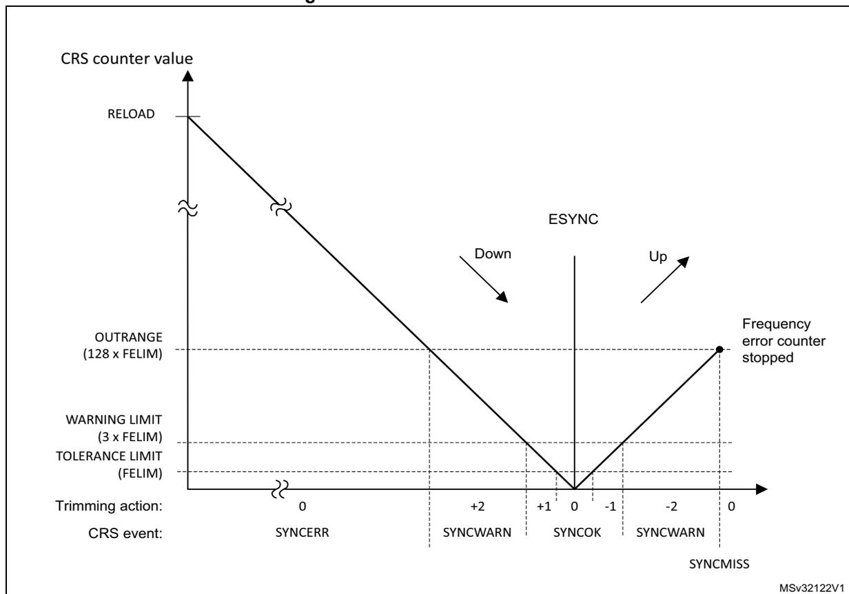
11.4.4 Frequency error measurement
The frequency error counter is a 16-bit down/up counter, reloaded with the RELOAD value on each SYNC event. It starts counting down until it reaches the zero value, where the ESYNC (expected synchronization) event is generated. Then it starts counting up to the OUTRANGE limit, where it eventually stops (if no SYNC event is received), and generates a SYNCMISS event. The OUTRANGE limit is defined as the frequency error limit (FELIM field of the CRS_CFGR register) multiplied by 128.
When the SYNC event is detected, the actual value of the frequency error counter and its counting direction are stored in the FECAP (frequency error capture) field and in the FEDIR (frequency error direction) bit of the CRS_ISR register. When the SYNC event is detected during the down-counting phase (before reaching the zero value), it means that the actual
frequency is lower than the target (the TRIM value must be incremented). When it is detected during the up-counting phase, it means that the actual frequency is higher (the TRIM value must be decremented).
Figure 35. CRS counter behavior
11.4.5 Frequency error evaluation and automatic trimming
The measured frequency error is evaluated by comparing its value with a set of limits:
- • TOLERANCE LIMIT, given directly in the FELIM field of the CRS_CFGR register
- • WARNING LIMIT, defined as \( 3 \times \text{FELIM} \) value
- • OUTRANGE (error limit), defined as \( 128 \times \text{FELIM} \) value
The result of this comparison is used to generate the status indication and also to control the automatic trimming, which is enabled by setting the AUTOTRIMEN bit in the CRS_CR register:
- • When the frequency error is below the tolerance limit, it means that the actual trimming value in the TRIM field is the optimal one, hence no trimming action is needed.
- – SYNCOK status indicated
- – TRIM value not changed in AUTOTRIM mode
- • When the frequency error is below the warning limit but above or equal to the tolerance limit, it means that some trimming action is necessary but that adjustment by one trimming step is enough to reach the optimal TRIM value.
- – SYNCOK status indicated
- – TRIM value adjusted by one trimming step in AUTOTRIM mode
- • When the frequency error is above or equal to the warning limit but below the error limit, a stronger trimming action is necessary, and there is a risk that the optimal TRIM value is not reached for the next period.
- – SYNCWARN status indicated
- – TRIM value adjusted by two trimming steps in AUTOTRIM mode
- • When the frequency error is above or equal to the error limit, the frequency is out of the trimming range. This can also happen when the SYNC input is not clean, or when some SYNC pulse is missing (for example when one USB SOF is corrupted).
- – SYNCERR or SYNCMISS status indicated
- – TRIM value not changed in AUTOTRIM mode
Note: If the actual value of the TRIM field is close to its limits and the automatic trimming can force it to overflow or underflow, the TRIM value is set to the limit, and the TRIMOVF status is indicated.
In AUTOTRIM mode (AUTOTRIMEN bit set in the CRS_CR register), the TRIM field of CRS_CR is adjusted by hardware and is read-only.
11.4.6 CRS initialization and configuration
RELOAD value
The RELOAD value must be selected according to the ratio between the target frequency and the frequency of the synchronization source after prescaling. This value is decreased by 1, to reach the expected synchronization on the zero value. The formula is the following:
The reset value of the RELOAD field corresponds to a target frequency of 48 MHz and a synchronization signal frequency of 1 kHz (SOF signal from USB).
FELIM value
The selection of the FELIM value is closely coupled with the HSI48 oscillator characteristics and its typical trimming step size. The optimal value corresponds to half of the trimming step size, expressed as a number of oscillator clock ticks. The following formula can be used:
The result must be always rounded up to the nearest integer value to obtain the best trimming response. If frequent trimming actions are not needed in the application, the hysteresis can be increased by slightly increasing the FELIM value.
The reset value of the FELIM field corresponds to \( (f_{\text{TARGET}} / f_{\text{SYNC}}) = 48000 \) , and to a typical trimming step size of 0.14%.
Note: The trimming step size depends upon the product, check the datasheet for accurate setting.
Caution: There is no hardware protection from a wrong configuration of the RELOAD and FELIM fields, this can lead to an erratic trimming response. The expected operational mode requires proper setup of the RELOAD value (according to the synchronization source frequency), which is also greater than \( 128 * \text{FELIM} \) value (OUTRANGE limit).
11.5 CRS in low-power modes
Table 111. Effect of low-power modes on CRS
| Mode | Description |
|---|---|
| Sleep | No effect. CRS interrupts cause the device to exit the Sleep mode. |
| Stop | CRS registers are frozen. The CRS stops operating until the Stop mode is exited and the HSI48 oscillator is restarted. |
| Standby | The peripheral is powered down and must be reinitialized after exiting Standby mode. |
11.6 CRS interrupts
Table 112. Interrupt control bits
| Interrupt event | Event flag | Enable control bit | Clear flag bit |
|---|---|---|---|
| Expected synchronization | ESYNCF | ESYNCIE | ESYNCC |
| Synchronization OK | SYNCOKF | SYNCOKIE | SYNCOKC |
| Synchronization warning | SYNCWARNF | SYNCWARNIE | SYNCWARNC |
| Synchronization or trimming error (TRIMOVF, SYNCMISS, SYNCERR) | ERRF | ERRIE | ERRC |
11.7 CRS registers
Refer to Section 1.2 for a list of abbreviations used in register descriptions.
The peripheral registers can be accessed only by words (32-bit).
11.7.1 CRS control register (CRS_CR)
Address offset: 0x00
Reset value: 0x0000 4000 (products supporting 7-bit TRIM width)
Reset value: 0x0000 2000 (other products)
| 31 | 30 | 29 | 28 | 27 | 26 | 25 | 24 | 23 | 22 | 21 | 20 | 19 | 18 | 17 | 16 |
|---|---|---|---|---|---|---|---|---|---|---|---|---|---|---|---|
| Res. | Res. | Res. | Res. | Res. | Res. | Res. | Res. | Res. | Res. | Res. | Res. | Res. | Res. | Res. | Res. |
| 15 | 14 | 13 | 12 | 11 | 10 | 9 | 8 | 7 | 6 | 5 | 4 | 3 | 2 | 1 | 0 |
| Res. | TRIM[6:0] | SW SYNC | AUTO TRIMEN | CEN | Res. | ESYNC IE | ERR IE | SYNC WARNIE | SYNC OKIE | ||||||
| rw | rw | rw | rw | rw | rw | rw | rl_w1 | rw | rw | rw | rw | rw | rw | ||
Bits 31:15 Reserved, must be kept at reset value.
Bits 14:8 TRIM[6:0] : HSI48 oscillator smooth trimmingThese bits provide a user-programmable trimming value to the HSI48 oscillator. They can be programmed to adjust to variations in voltage and temperature that influence the oscillator frequency.
The default value of the HSI48 oscillator smooth trimming is 64, for a complete TRIM range of 128 steps.
The trimming step is specified in the product datasheet. A higher TRIM value corresponds to a higher output frequency.
When the AUTOTRIMEN bit is set, this field is controlled by hardware and is read-only.
Bit 7 SWSYNC : Generate software SYNC eventThis bit is set by software in order to generate a software SYNC event. It is automatically cleared by hardware.
0: No action
1: A software SYNC event is generated.
Bit 6 AUTOTRIMEN : Automatic trimming enableThis bit enables the automatic hardware adjustment of TRIM bits according to the measured frequency error between two SYNC events. If this bit is set, the TRIM bits are read-only. The TRIM value can be adjusted by hardware by one or two steps at a time, depending on the measured frequency error value. Refer to Section 11.4.5 for more details.
0: Automatic trimming disabled, TRIM bits can be adjusted by the user.
1: Automatic trimming enabled, TRIM bits are read-only and under hardware control.
Bit 5 CEN : Frequency error counter enableThis bit enables the oscillator clock for the frequency error counter.
0: Frequency error counter disabled
1: Frequency error counter enabled
When this bit is set, the CRS_CFGR register is write-protected and cannot be modified.
Bit 4 Reserved, must be kept at reset value.
Bit 3 ESYNCIE : Expected SYNC interrupt enable0: Expected SYNC (ESYNCF) interrupt disabled
1: Expected SYNC (ESYNCF) interrupt enabled
Bit 2 ERRIE : Synchronization or trimming error interrupt enable0: Synchronization or trimming error (ERRF) interrupt disabled
1: Synchronization or trimming error (ERRF) interrupt enabled
Bit 1 SYNCWARNIE : SYNC warning interrupt enable0: SYNC warning (SYNCWARNF) interrupt disabled
1: SYNC warning (SYNCWARNF) interrupt enabled
Bit 0 SYNCOKIE : SYNC event OK interrupt enable0: SYNC event OK (SYNCOKF) interrupt disabled
1: SYNC event OK (SYNCOKF) interrupt enabled
11.7.2 CRS configuration register (CRS_CFGR)
This register can be written only when the frequency error counter is disabled (the CEN bit is cleared in CRS_CR). When the counter is enabled, this register is write-protected.
Address offset: 0x04
Reset value: 0x2022 BB7F
| 31 | 30 | 29 | 28 | 27 | 26 | 25 | 24 | 23 | 22 | 21 | 20 | 19 | 18 | 17 | 16 |
|---|---|---|---|---|---|---|---|---|---|---|---|---|---|---|---|
| SYNCPOL | Res. | SYNCSRC[1:0] | Res. | SYNCDIV[2:0] | FELIM[7:0] | ||||||||||
| rw | rw | rw | rw | rw | rw | rw | rw | rw | rw | rw | rw | rw | rw | ||
| 15 | 14 | 13 | 12 | 11 | 10 | 9 | 8 | 7 | 6 | 5 | 4 | 3 | 2 | 1 | 0 |
| RELOAD[15:0] | |||||||||||||||
| rw | rw | rw | rw | rw | rw | rw | rw | rw | rw | rw | rw | rw | rw | rw | rw |
Bit 31 SYNCPOL : SYNC polarity selection
This bit is set and cleared by software to select the input polarity for the SYNC signal source.
0: SYNC active on rising edge (default)
1: SYNC active on falling edge
Bit 30 Reserved, must be kept at reset value.
Bits 29:28 SYNCSRC[1:0] : SYNC signal source selection
These bits are set and cleared by software to select the SYNC signal source (see Section 11.4.2: CRS internal signals ).
00: crs_sync_in_0 selected as SYNC signal source
01: crs_sync_in_1 selected as SYNC signal source
10: crs_sync_in_2 selected as SYNC signal source
11: crs_sync_in_3 selected as SYNC signal source
Note: When using USB LPM (link power management) and the device is in Sleep mode, the periodic USB SOF is not generated by the host. No SYNC signal is therefore provided to the CRS to calibrate the 48 MHz clock on the run. To guarantee the required clock precision after waking up from Sleep mode, the LSE clock or the SYNC pin must be used as SYNC signal.
Bit 27 Reserved, must be kept at reset value.
Bits 26:24 SYNCDIV[2:0] : SYNC divider
These bits are set and cleared by software to control the division factor of the SYNC signal.
000: SYNC not divided (default)
001: SYNC divided by 2
010: SYNC divided by 4
011: SYNC divided by 8
100: SYNC divided by 16
101: SYNC divided by 32
110: SYNC divided by 64
111: SYNC divided by 128
Bits 23:16 FELIM[7:0] : Frequency error limit
FELIM contains the value to be used to evaluate the captured frequency error value latched in the FECAP[15:0] bits of the CRS_ISR register. Refer to Section 11.4.5 for more details about FECAP evaluation.
Bits 15:0 RELOAD[15:0] : Counter reload value
RELOAD is the value to be loaded in the frequency error counter with each SYNC event.
Refer to Section 11.4.4 for more details about counter behavior.
11.7.3 CRS interrupt and status register (CRS_ISR)
Address offset: 0x08
Reset value: 0x0000 0000
| 31 | 30 | 29 | 28 | 27 | 26 | 25 | 24 | 23 | 22 | 21 | 20 | 19 | 18 | 17 | 16 |
|---|---|---|---|---|---|---|---|---|---|---|---|---|---|---|---|
| FECAP[15:0] | |||||||||||||||
| r | r | r | r | r | r | r | r | r | r | r | r | r | r | r | r |
| 15 | 14 | 13 | 12 | 11 | 10 | 9 | 8 | 7 | 6 | 5 | 4 | 3 | 2 | 1 | 0 |
| FEDIR | Res. | Res. | Res. | Res. | TRIM OVF | SYNC MISS | SYNC ERR | Res. | Res. | Res. | Res. | ESYNCF | ERRF | SYNC WARNF | SYNC OKF |
| r | r | r | r | r | r | r | r | ||||||||
Bits 31:16 FECAP[15:0] : Frequency error capture
FECAP is the frequency error counter value latched in the time of the last SYNC event.
Refer to Section 11.4.5 for more details about FECAP usage.
Bit 15 FEDIR : Frequency error direction
FEDIR is the counting direction of the frequency error counter latched in the time of the last SYNC event. It shows whether the actual frequency is below or above the target.
0: Up-counting direction, the actual frequency is above the target
1: Down-counting direction, the actual frequency is below the target
Bits 14:11 Reserved, must be kept at reset value.
Bit 10 TRIMOVF : Trimming overflow or underflow
This flag is set by hardware when the automatic trimming tries to over- or under-flow the TRIM value. An interrupt is generated if the ERRRIE bit is set in the CRS_CR register. It is cleared by software by setting the ERRRC bit in the CRS_ICR register.
0: No trimming error signaled
1: Trimming error signaled
Bit 9 SYNCMISS : SYNC missed
This flag is set by hardware when the frequency error counter reaches value FELIM * 128 and no SYNC is detected, meaning either that a SYNC pulse was missed, or the frequency error is too big (internal frequency too high) to be compensated by adjusting the TRIM value, hence some other action must be taken. At this point, the frequency error counter is stopped (waiting for a next SYNC), and an interrupt is generated if the ERRRIE bit is set in the CRS_CR register. It is cleared by software by setting the ERRRC bit in the CRS_ICR register.
0: No SYNC missed error signaled
1: SYNC missed error signaled
Bit 8 SYNCERR: SYNC errorThis flag is set by hardware when the SYNC pulse arrives before the ESYNC event and the measured frequency error is greater than or equal to \( FELIM * 128 \) . This means that the frequency error is too big (internal frequency too low) to be compensated by adjusting the TRIM value, and that some other action has to be taken. An interrupt is generated if the ERRIE bit is set in the CRS_CR register. It is cleared by software by setting the ERRC bit in the CRS_ICR register.
0: No SYNC error signaled
1: SYNC error signaled
Bits 7:4 Reserved, must be kept at reset value.
Bit 3 ESYNCF: Expected SYNC flagThis flag is set by hardware when the frequency error counter reached a zero value. An interrupt is generated if the ESYNCIE bit is set in the CRS_CR register. It is cleared by software by setting the ESYNCC bit in the CRS_ICR register.
0: No expected SYNC signaled
1: Expected SYNC signaled
Bit 2 ERRF: Error flagThis flag is set by hardware in case of any synchronization or trimming error. It is the logical OR of the TRIMOVF, SYNCMISS and SYNCERR bits. An interrupt is generated if the ERRIE bit is set in the CRS_CR register. It is cleared by software in reaction to setting the ERRC bit in the CRS_ICR register, which clears the TRIMOVF, SYNCMISS and SYNCERR bits.
0: No synchronization or trimming error signaled
1: Synchronization or trimming error signaled
Bit 1 SYNCWARNF: SYNC warning flagThis flag is set by hardware when the measured frequency error is greater than or equal to \( FELIM * 3 \) , but smaller than \( FELIM * 128 \) . This means that to compensate the frequency error, the TRIM value must be adjusted by two steps or more. An interrupt is generated if the SYNCWARNIE bit is set in the CRS_CR register. It is cleared by software by setting the SYNCWARNC bit in the CRS_ICR register.
0: No SYNC warning signaled
1: SYNC warning signaled
Bit 0 SYNCOKF: SYNC event OK flagThis flag is set by hardware when the measured frequency error is smaller than \( FELIM * 3 \) . This means that either no adjustment of the TRIM value is needed or that an adjustment by one trimming step is enough to compensate the frequency error. An interrupt is generated if the SYNCOKIE bit is set in the CRS_CR register. It is cleared by software by setting the SYNCOKC bit in the CRS_ICR register.
0: No SYNC event OK signaled
1: SYNC event OK signaled
11.7.4 CRS interrupt flag clear register (CRS_ICR)
Address offset: 0x0C
Reset value: 0x0000 0000
| 31 | 30 | 29 | 28 | 27 | 26 | 25 | 24 | 23 | 22 | 21 | 20 | 19 | 18 | 17 | 16 |
| Res. | Res. | Res. | Res. | Res. | Res. | Res. | Res. | Res. | Res. | Res. | Res. | Res. | Res. | Res. | Res. |
| 15 | 14 | 13 | 12 | 11 | 10 | 9 | 8 | 7 | 6 | 5 | 4 | 3 | 2 | 1 | 0 |
| Res. | Res. | Res. | Res. | Res. | Res. | Res. | Res. | Res. | Res. | Res. | Res. | ESYNCC | ERRC | SYNC WARNC | SYNC OKC |
| rw | rw | rw | rw | ||||||||||||
Bits 31:4 Reserved, must be kept at reset value.
Bit 3
ESYNCC
: Expected SYNC clear flag
Writing 1 to this bit clears the ESYNCF flag in the CRS_ISR register.
Bit 2
ERRC
: Error clear flag
Writing 1 to this bit clears TRIMOVF, SYNCMISS, and SYNCERR bits and consequently also the ERRF flag in the CRS_ISR register.
Bit 1
SYNCWARNC
: SYNC warning clear flag
Writing 1 to this bit clears the SYNCWARNF flag in the CRS_ISR register.
Bit 0
SYNCOKC
: SYNC event OK clear flag
Writing 1 to this bit clears the SYNCOKF flag in the CRS_ISR register.
11.7.5 CRS register map
Table 113. CRS register map and reset values
| Offset | Register name | 31 | 30 | 29 | 28 | 27 | 26 | 25 | 24 | 23 | 22 | 21 | 20 | 19 | 18 | 17 | 16 | 15 | 14 | 13 | 12 | 11 | 10 | 9 | 8 | 7 | 6 | 5 | 4 | 3 | 2 | 1 | 0 | |
|---|---|---|---|---|---|---|---|---|---|---|---|---|---|---|---|---|---|---|---|---|---|---|---|---|---|---|---|---|---|---|---|---|---|---|
| 0x00 | CRS_CR | Res. | TRIM[6:0] | SWSYNC | AUTOTRIMEN | CEN | Res. | ESYNCIE | ERRIE | SYNCWARNIE | SYNCOKIE | |||||||||||||||||||||||
| Reset value | 0x0000 4000 (products supporting 7-bit TRIM width) 0x0000 2000 (other products) | |||||||||||||||||||||||||||||||||
| 0x04 | CRS_CFGR | SYNCPOL | Res. | SYNCS RC[1:0] | Res. | SYNCDIV [2:0] | FELIM[7:0] | RELOAD[15:0] | ||||||||||||||||||||||||||
| Reset value | 0 | 1 | 0 | 0 | 0 | 0 | 0 | 0 | 1 | 0 | 0 | 0 | 1 | 0 | 1 | 0 | 1 | 1 | 1 | 0 | 1 | 1 | 0 | 1 | 1 | 1 | 1 | 1 | 1 | 1 | ||||
| 0x08 | CRS_ISR | FECAP[15:0] | FEDIR | Res. | TRIMOVF | SYNCMISS | SYNCERR | Res. | ESYNCF | ERRF | SYNCWARNF | SYNCOKF | ||||||||||||||||||||||
| Reset value | 0 | 0 | 0 | 0 | 0 | 0 | 0 | 0 | 0 | 0 | 0 | 0 | 0 | 0 | 0 | 0 | 0 | 0 | 0 | 0 | 0 | 0 | 0 | 0 | ||||||||||
Table 113. CRS register map and reset values (continued)
| Offset | Register name | 31 | 30 | 29 | 28 | 27 | 26 | 25 | 24 | 23 | 22 | 21 | 20 | 19 | 18 | 17 | 16 | 15 | 14 | 13 | 12 | 11 | 10 | 9 | 8 | 7 | 6 | 5 | 4 | 3 | 2 | 1 | 0 | |
|---|---|---|---|---|---|---|---|---|---|---|---|---|---|---|---|---|---|---|---|---|---|---|---|---|---|---|---|---|---|---|---|---|---|---|
| 0x0C | CRS_ICR | Res. | Res. | Res. | Res. | Res. | Res. | Res. | Res. | Res. | Res. | Res. | Res. | Res. | Res. | Res. | Res. | Res. | Res. | Res. | Res. | Res. | Res. | Res. | Res. | Res. | Res. | Res. | Res. | Res. | ESYNCC | ERRC | SYNCWARNC | SYNCOKC |
| Reset value | 0 | 0 | 0 | 0 |
Refer to Section 2.3: Memory organization for the register boundary addresses.