10. Reset and clock control (RCC)
10.1 RCC introduction
The reset and clock control (RCC) manages the different kinds of reset, and generates all clocks for the bus and peripherals.
10.2 RCC functional description
10.2.1 RCC pins and internal signals
The table below lists the RCC inputs and output signals connected to package pins or balls.
Table 99. RCC input/output signals connected to package pins or balls
| Pin name | Pin type | Description |
|---|---|---|
| NRST | I/O | System reset, can be used to provide reset to external devices |
| OSC32_IN | I | 32 kHz oscillator input |
| OSC32_OUT | O | 32 kHz oscillator output |
| OSC_IN | I | System oscillator input |
| OSC_OUT | O | System oscillator output |
| MCO | O | Output clock for external devices |
| MCO2 | O | Output clock 2 for external devices |
| LSCO | O | Low-speed output clock for external devices |
| AUDIOCLK | I | External kernel clock input for SAI1 and ADF1 |
10.2.2 RCC reset functional description
There are three types of reset:
- • a system reset
- • a power reset
- • a backup domain reset
Power reset
A power reset is generated when one of the following events occurs:
- • a brownout reset (BOR)
- • when exiting Standby mode
- • when exiting Shutdown mode
A BOR sets all registers to their reset values except the ones in the backup domain.
When exiting Standby mode, all registers in the core domain are set to their reset value. Registers outside the core domain (RTC, TAMP, WKUP, IWDG, and Standby/Shutdown mode control) are not impacted.
When exiting Shutdown mode, a brownout reset is generated, resetting all registers except those in the backup domain.
System reset
A system reset sets all registers to their reset values except the reset flags in RCC_CSR, and the registers in the backup domain.
A system reset is generated when one of the following events occurs:
- • a low level on the NRST pin (external reset)
- • a window watchdog event (WWDG reset)
- • an independent watchdog event (IWDG reset)
- • a software reset (SW reset)
- • a low-power mode security reset
- • an option-byte loader reset
- • a brownout reset
The reset source can be identified by checking the reset flags in RCC_CSR.
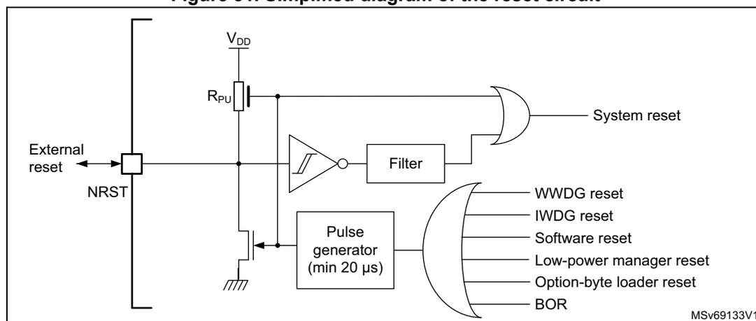
These sources act on the NRST pin and this pin is always kept low during the delay phase. The reset service routine vector is selected via the boot option bytes.
The system reset signal provided to the device is output on the NRST pin. The pulse generator guarantees a minimum reset pulse duration of 20 µs for each internal reset source. In case of an external reset, the reset pulse is generated while the NRST pin is asserted low.
In case of an internal reset, the internal pull-up R PU is deactivated in order to save the power consumption through the pull-up resistor.
Figure 31. Simplified diagram of the reset circuit
- • Software reset
The SYSRESETREQ bit in Cortex-M33 application interrupt and reset control register must be set to force a software reset on the device.
- • Low-power mode security reset
To avoid that critical applications mistakenly enter a low-power mode, the following low-power mode security resets are available. If enabled in option bytes, the resets are generated in any of the following conditions:
- – Entering Standby mode: this type of reset is enabled by resetting NRST_STDBY bit in user option bytes. In this case, whenever a Standby mode entry sequence is successfully executed, the device is reset instead of entering Standby mode.
- – Entering Stop mode: this type of reset is enabled by resetting NRST_STOP bit in user option bytes. In this case, whenever a Stop mode entry sequence is successfully executed, the device is reset instead of entering Stop mode.
- – Entering Shutdown mode: this type of reset is enabled by resetting NRST_SHDW bit in user option bytes. In this case, whenever a Shutdown mode entry sequence is successfully executed, the device is reset instead of entering Shutdown mode.
For further information on the user option bytes, refer to Section 7.4.2: Option-byte programming .
- • Option byte loader reset
The option byte loader reset is generated when the OBL_LAUNCH bit is set in FLASH_CR. This bit is used to launch the option byte loading by software.
Backup domain reset
The backup domain has two specific resets.
A backup domain reset is generated when one of the following events occurs:
- • a software reset, triggered by setting the BDRST bit in RCC_BDCR
- • a V DD or V BAT power on, if both supplies have previously been powered off
A backup domain reset affects the LSE oscillator, the RTC, the TAMP, the backup registers, and RCC_BDCR.
10.2.3 RCC clock functional description
Three different clock sources can be used to drive the system clock (SYSCLK):
- • HSI16: high-speed internal 16 MHz RC oscillator clock
- • MSIS: multi-speed internal RC oscillator clock, from 3 to 96 MHz
- • HSE: high-speed external crystal or clock, from 4 to 50 MHz
The MSIS is used as system clock source after startup from reset, configured at 12 MHz.
The devices have the following additional clock sources:
- • MSIK: multi-speed internal RC oscillator clock used for peripherals kernel clocks, from 3 to 96 MHz
- • LSI: 32 kHz/250 Hz low-speed internal RC that drives the independent watchdog and optionally the RTC used for automatic wake-up from Stop and Standby modes
- • LSE: 32.768 kHz low-speed external crystal or clock that optionally drives the real-time clock (rtc_ck)
- • HSI48: internal 48 MHz RC that potentially drives the USB, the SDMMC and the RNG
Each clock source can be switched on or off independently when it is not used, to optimize power consumption.
Several prescalers can be used to configure the AHB frequency, the APB1, APB2, and APB3 domains. The maximum frequency of the AHB and APB domains is 96 MHz.
All peripheral clocks are derived from their bus clock (HCLK, PCLK1, PCLK2, or PCLK3), except the following ones that receive an independent kernel clock: USB, SDMMC1, RNG, ADCx (x = 1, 2), DAC1, U(S)ARTx (x = 1 to 5), LPUART1, I2Cx (x = 1 to 4), I3Cx (x = 1, 2), SPIx (x = 1 to 4), OCTOSPI1, SAI1, ADF1, FDCANx, LPTIMx (x = 1 to 4). Most of these kernel clocks can be selected by software from various sources, thanks to RCC_CCIPRx registers (x = 1 to 3).
In addition, the RTC kernel clock is selected by software in RCC_BDCR. The IWDG clock is always the LSI 32 kHz clock.
The RCC feeds the core system timer (SysTick) external clock with the AHB clock (HCLK) divided by eight, or LSE, or LSI. The SysTick can work either with this clock or directly with the core clock (HCLK), configurable in the SysTick control and status register.
FCLK acts as Cortex-M33 free-running clock.
Figure 32. Clock tree (1)
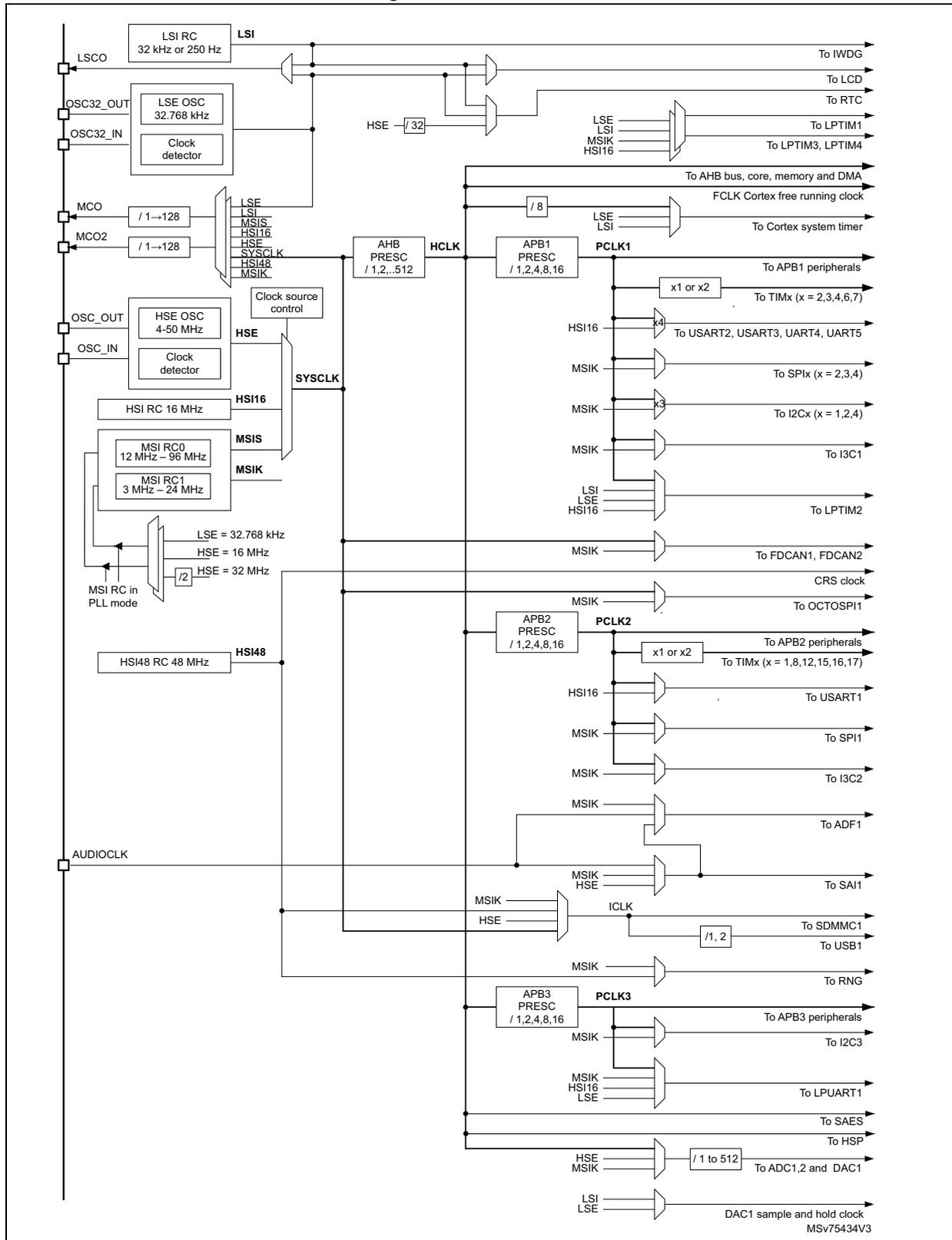
The diagram illustrates the internal clock architecture of the microcontroller. On the left, various clock sources are shown:
- LSI : LSI RC (32 kHz or 250 Hz) connected to LSCO and various multiplexers.
- LSE : LSE OSC (32.768 kHz) connected to OSC32_OUT and OSC32_IN, with an associated clock detector.
- HSE : HSE OSC (4-50 MHz) connected to OSC_OUT and OSC_IN, with an associated clock detector.
- HSI16 : HSI RC 16 MHz.
- MSI : MSI RC0 (12 MHz – 96 MHz) and MSI RC1 (3 MHz – 24 MHz), providing MSIS and MSIK signals.
- PLL : MSI RC in PLL mode, with inputs for LSE = 32.768 kHz, HSE = 16 MHz, and HSE = 32 MHz (divided by /2).
- HSI48 : HSI48 RC 48 MHz.
- AUDIOCLK : External audio clock input.
- MCO and MCO2 : Output clocks with prescalers (/1–128) selectable from various sources.
- AHB PRESC (/1, 2, ..., 512): Generates HCLK for the AHB bus, core, memory, and DMA. It also provides the FCLK Cortex free running clock.
- APB1 PRESC (/1, 2, 4, 8, 16): Generates PCLK1 . It includes a /8 divider for the Cortex system timer and feeds APB1 peripherals, timers (TIMx), and various communication interfaces (USART, SPI, I2C, I3C, LPTIM2, FDCAN, CRS).
- APB2 PRESC (/1, 2, 4, 8, 16): Generates PCLK2 . It feeds APB2 peripherals, timers (TIMx), USART1, SPI1, I3C2, ADF1, SAI1, SDMMC1, USB1, and RNG.
- APB3 PRESC (/1, 2, 4, 8, 16): Generates PCLK3 . It feeds APB3 peripherals, I2C3, LPUART1, SAES, HSP, ADC1,2, and DAC1.
1. Some peripherals are not available on all devices. Refer to the product specific datasheet.
HSE clock
The high-speed external clock signal (HSE) can be generated from two possible clock sources:
- • HSE external crystal/ceramic resonator
- • HSE user external clock
The resonator and the load capacitors must be placed as close as possible to the oscillator pins in order to minimize output distortion and startup stabilization time. The loading capacitance values must be adjusted according to the selected oscillator.
Table 100. HSE/LSE clock sources
| Clock source | Hardware configuration |
|---|---|
| External clock | Image: Diagram showing an external clock source connected to the OSC_IN pin, while the OSC_OUT pin is configured as a GPIO. graph LR
S[External clock source] --> OSC_IN
OSC_OUT --> GPIO |
| Crystal/ceramic resonators | Image: Diagram showing a crystal or ceramic resonator connected between OSC_IN and OSC_OUT pins. Two load capacitors, CL1 and CL2, connect each pin to ground. graph TD
OSC_IN --- R[Resonator]
R --- OSC_OUT
OSC_IN --- CL1[CL1]
OSC_OUT --- CL2[CL2]
CL1 --- G[Ground]
CL2 --- G |
- • External crystal/ceramic resonator (HSE crystal)
The external oscillator has the advantage of producing a very accurate rate on the main clock.
The associated hardware configuration is shown in Table 100: HSE/LSE clock sources . Refer to the electrical characteristics section of the datasheet for more details.
The HSERDY flag in RCC_CR indicates if the HSE oscillator is stable or not. At startup, the clock is not released until this bit is set by hardware. An interrupt can be generated if enabled in RCC_CIER .
The HSE crystal can be switched on and off using the HSEON bit in RCC_CR .
- • External source (HSE bypass)
In this mode, an external clock source must be provided. This mode is selected by setting the HSEBYP and HSEON bits in RCC_CR . The external clock signal with
~40 - 60 % duty cycle depending on the frequency (refer to the datasheet) must drive the OSC_IN pin while the OSC_OUT pin can be used a GPIO (see Table 100: HSE/LSE clock sources ). The bypass mode is optimized for square input signals when HSEEXT = 1. If the input is a sine wave or triangle signal, HSEEXT must be kept at 0 (analog bypass mode).
HSI16 clock
The HSI16 clock signal is generated from an internal 16 MHz RC oscillator.
The HSI16 RC oscillator has the advantage of providing a clock source at low cost (no external components). It also has a faster startup time than the HSE crystal oscillator. However, even with calibration, the frequency is less accurate than an external crystal oscillator or ceramic resonator.
The HSI16 clock can be selected as system clock after wake-up from Stop modes (Stop 0, Stop 1, Stop 2, or Stop 3). Refer to RCC_CFGR1 . It can also be used as a backup clock source (auxiliary clock) if the HSE crystal oscillator fails. Refer to Clock security system (CSS) .
- • HSI16 calibration
The RC oscillator frequencies may vary from one chip to another due to manufacturing process variations, this is why each device is factory calibrated by ST for 1 % accuracy at \( T_A = 25^\circ\text{C} \) .
After reset, the factory calibration value is loaded in the HSICAL[11:0] bits in RCC_ICSCR3 .
If the application is subject to voltage or temperature variations, this may affect the RC oscillator speed. The HSI16 frequency can be trimmed in the application using the HSITRIM[4:0] in RCC_ICSCR3 .
For more details on how to measure the HSI16 frequency variation, refer to Internal/external clock measurement with TIM15/TIM16/TIM17 .
The HSI16RDY flag in RCC_CR indicates if the HSI16 RC is stable or not. At startup, the HSI16 RC output clock is not released until this bit is set by hardware.
The HSI16 RC can be switched on and off using the HSION bit in RCC_CR .
The HSI16 signal can also be used as a backup source (Auxiliary clock) if the HSE crystal oscillator fails. Refer to Clock security system (CSS) .
MSI (MSIS and MSIK) clocks
The MSI is made of two internal RC oscillators: MSIRC0 at 96 MHz and MSIRC1 at 24 MHz. Each oscillator feeds a prescaler providing a division by 1, 2, 4, or 8. Two output clocks are generated from these divided oscillators: MSIS, that can be selected as system clock, and MSIK, that can be selected by some peripherals as kernel clock.
Figure 33. MSI block diagram
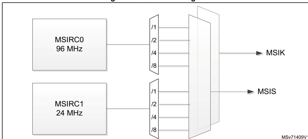
For each output clock MSIS and MSIK, the oscillator source is selected using respectively MSISSEL and MSIKSEL, and division factor is selected using respectively MSISDIV[1:0] and MSIKDIV[1:0] in RCC_ICSCR1. A total of six different frequencies are available, generated from the two internal RCs, as shown in Table 101 . 24 MHz and 12 MHz can be generated from both RCs.
In case no higher frequency is needed in the application, it is recommended to select MSIRC1 to get lower consumption.
In case 48 MHz or 96 MHz frequency is also needed in addition to 24 or 12 MHz, it is recommended to select MSIRC0, and generate both frequencies from the same oscillator rather than using both RCs, in order to save additional RC consumption.
Table 101. MSIS and MSIK ranges per internal MSIRCs (PLL mode disabled)
| MSIRC0 | MSIRC1 |
|---|---|
| Range 0: 96 MHz | Range 4: 24 MHz |
| Range 1: 48 MHz | Range 5: 12 MHz |
| Range 2: 24 MHz | Range 6: 6 MHz |
| Range 3: 12 MHz | Range 7: 3 MHz |
Note: Refer to datasheet for complete MSI frequency characteristics in MSI-mode and in PLL mode.
The MSIS clock is used as system clock after restart from reset, wake-up from Standby and Shutdown low-power modes. After restart from reset or when exiting Shutdown mode, the MSIS and MSIK frequencies are set to their default value 12 MHz, generated from MSIRC1. The selected oscillator is always MSIRC1 when exiting Standby mode, and the frequency range can be adjusted by software between 3, 6 or 12 MHz, using respectively the MSISDIVS[1:0] and MSIKDIVS[1:0] fields. Refer to RCC_CSR.
The MSIS clock can be selected as system clock after a wake-up from Stop mode (Stop 0, Stop 1, Stop 2, or Stop 3) depending on STOPWUCK in RCC_CFGR1. It can also be used
as a backup clock source (auxiliary clock) if the HSE crystal oscillator fails. Refer to Clock security system (CSS) .
The MSI oscillator has the advantage of providing a low-cost (no external components) low-power clock source. In addition, when used in PLL mode with the LSE or HSE, the MSI provides a very accurate clock source that can be used by the USB peripheral.
MSISRDY and MSIKRDY flags in RCC_CR indicate whether the MSIS and MSIK RC are stable or not. At startup, the MSIS and MSIK RC output clocks are not released until their respective bit is set by hardware. The MSIS and MSIK RC can be switched on and off by using the MSISON and MSIKON bits in RCC_CR.
- • Hardware auto-calibration with LSE or HSE (PLL mode)
When a 32.768 kHz, a 32 MHz or a 16 MHz external oscillator is present in the application, it is possible to configure MSIS, MSIK or both in a PLL mode. The long term accuracy of the MSI in PLL mode is the one of the external oscillator.
Using the MSI in PLL mode with LSE provides a low-power solution to get an accurate high-speed clock.
The MSIS is in PLL mode when the internal MSIRCx (x = 0, 1) selected for MSIS is configured in PLL mode. The MSIK is in PLL mode when the internal MSIRCx (x = 0, 1) selected for MSIK is configured in PLL mode.
Either MSIS or MSIK, with MSIRC1 selected, must be enabled and ready before enabling MSIRC1 PLL mode, and in the same way either MSIS or MSIK, with MSIRC0 selected, must be enabled and ready before enabling MSIRC0 PLL mode.
When LSE or HSE is used for PLL mode, this oscillator must be enabled and ready before selecting it as input for MSIRCx PLL mode.
MSIRCx PLL mode is configured to operate with LSE when the corresponding MSIPLLxSEL = 0, or with HSE at 32 MHz or 16 MHz when the corresponding MSIPLLxSEL = 1 in RCC_ICSCR1. In case HSE is at 32 MHz, it must be divided by 2 by setting MSIHSINDIV bit.
Once input clock is selected, the MSIRCx PLL mode is enabled by setting the corresponding MSIPLLxEN bit in RCC_CR. Refer to Table 102 for an overview of available frequencies in this mode.
If the PLL input clock (LSE or HSE) pulses are stopped or temporarily disturbed, the MSI PLL mode is automatically unlocked, and the MSI accuracy is consequently degraded. If enabled in RCC_CIER, an interrupt is generated. The MSI PLL mode with LSE unlock interrupt can wake up from Stop 0, Stop 1 and Stop 2 modes. To reconfigure the MSI in PLL mode, the MSIPLLxEN (x = 0, 1) bit in RCC_CR must be cleared and set again.
When MSIRC1 is used in PLL mode, the reached frequency can be selected thanks to MSIPLL1N[1:0] bitfield in the RCC_ICSR1. Those additional frequencies are useful for audio applications.
Table 102. MSIS and MSIK frequencies of MSIRC1 in PLL mode
| MSI range | MSISDIV[1:0] or MSIKDIV[1:0] | PLL range MSIPLL1N[1:0] | MSIPLL1SEL = 0: LSE | MSIPLL1SEL = 1: HSE or HSE/2 |
|---|---|---|---|---|
| Range 0: MSISSEL = 0 or MSIKSEL = 0 | 00: MSIRC0/1 | XX | 96.010 MHz | 96.0 MHz |
| 01: MSIRC0/2 | XX | 48.005 MHz | 48.0 MHz | |
| 10: MSIRC0/4 | XX | 24.003 MHz | 24.0 MHz | |
| 11: MSIRC0/8 | XX | 12.001 MHz | 12.0 MHz | |
| Range 1: MSISSEL = 1 or MSIKSEL = 1 | 00: MSIRC1/1 | 0X | 23.986 MHz | 24.016 MHz |
| 10 | 22.577 MHz | 22.581 MHz | ||
| 11 | 24.576 MHz | 24.577 MHz | ||
| 01: MSIRC1/2 | 0X | 11.993 MHz | 12.008 MHz | |
| 10 | 11.289 MHz | 11.290 MHz | ||
| 11 | 12.288 MHz | 12.289 MHz | ||
| 10: MSIRC1/4 | 0X | 5.997 MHz | 6.004 MHz | |
| 10 | 5.644 MHz | 5.645 MHz | ||
| 11 | 6.144 MHz | 6.144 MHz | ||
| 11: MSIRC1/8 | 0X | 2.998 MHz | 3.002 MHz | |
| 10 | 2.822 MHz | 2.823 MHz | ||
| 11 | 3.072 MHz | 3.072 MHz |
- MSI PLL mode stabilization time
When MSIPLLxEN (x = 0,1) = 1, the final accuracy after enabling the MSI (by writing MSISON = 1 or MSIKON = 1 or following a peripheral clock request in Stop mode) is reached after a stabilization time \( t_{STAB}(MSI) \) when the corresponding MSIPLLxFAST = 0. This stabilization time is needed even if the input clock (LSE or HSE) is kept enable. Refer to datasheet for \( t_{STAB}(MSI) \) value.
If MSIPLLxEN = 1 with MSIPLLxFAST = 1, the MSI oscillator is kept powered on when a request to switch it off is received (either by writing MSISON = 0 and MSIKON = 0, or because no peripheral requests this clock in Stop mode). In this case the MSI PLL mode accuracy is kept when the MSI is switched on again, providing that the \( t_{STAB}(MSI) \) stabilization time is reached before switching off the MSI. This mode can be used for autonomous peripherals requiring accuracy in Stop mode, with an extra consumption as the oscillator remains powered on, but gated off when disabled.
Note: MSI PLL mode fast stabilization time feature is not functional in Stop 3 mode. Basic PLL mode stabilization time will be required on Stop 3 mode exit.
- Software calibration
The MSIRCx (x = 0,1) oscillators frequency may vary from one chip to another due to manufacturing process variations, this is why each device is factory calibrated by ST for 1 % accuracy at an ambient temperature, \( T_A = 25\ ^\circ C \) . After reset, the factory calibration value is loaded in the MSICALx[5:0] bits (x = 0,1) in RCC_ICSCR1. If the application is subject to voltage or temperature variations, this may affect the RC
oscillator speed. The MSIRCx frequency can be trimmed in the application by using the MSITRIMx[5:0] bits (x = 0,1) in RCC_ICSCR2.
Note: The final accuracy after applying the calibration value is reached after a stabilization time. This stabilization time is needed after reset or exiting Standby or Shutdown mode. It is also needed when switching from PLL mode to normal mode.
The hardware auto-calibration with LSE or HSE must not be used in conjunction with software calibration.
For more details on how to measure the MSI frequency variation, refer to Internal/external clock measurement with TIM15/TIM16/TIM17 .
HSI48 clock
The HSI48 clock signal is generated from an internal 48 MHz RC oscillator and can be used directly for USB and for random number generator (RNG) as well as SDMMC.
The internal 48 MHz RC oscillator is mainly dedicated to provide a high-precision clock to the USB peripheral by means of a special clock recovery system (CRS) circuitry. The CRS can use the USB SOF signal, the LSE or an external signal to automatically and quickly adjust the oscillator frequency on-fly. It is disabled as soon as the system enters Stop or Standby mode. When the CRS is not used, the HSI48 RC oscillator runs on its default frequency that is subject to manufacturing process variations.
For more details on how to configure and use the CRS peripheral, refer to Section 11: Clock recovery system (CRS) .
The HSI48RDY flag in RCC_CR indicates whether the HSI48 RC oscillator is stable or not. At startup, the HSI48 RC oscillator output clock is not released until this bit is set by hardware.
The HSI48 can be switched on and off using the HSI48ON bit in RCC_CR.
LSE clock
The LSE crystal is a 32.768 kHz low-speed external crystal or ceramic resonator. It has the advantage of providing a low-power but highly accurate clock source to the real-time clock peripheral (RTC) for clock/calendar or other timing functions.
The LSE crystal is switched on and off using the LSEON bit in RCC_BDCR. If the LSE is used by other peripherals or functions than RTC, TAMP, and LSECSS, the LSESYSEN bit must be also be set in RCC_BDCR (refer to LSE when used by peripherals other than RTC/TAMP, and RCC functions ).
The crystal oscillator driving strength is configured using the LSEDRV[1:0] bits, according to crystal specification, to obtain the best compromise between robustness and short startup time on one side and low-power-consumption on the other side. The LSE drive must be programmed before enabling the LSE.
The LSERDY flag in RCC_BDCR indicates whether the LSE crystal is stable or not. At startup, the LSE crystal output clock signal is not released until this bit is set by hardware. An interrupt can be generated if enabled in RCC_CIER.
- • External source (LSE bypass)
In this mode, an external clock source must be provided. This mode is selected by setting the LSEBYP and LSEON bits in RCC_BDCR. The external clock signal (square, sinus or triangle) with ~50 % duty cycle, must drive the OSC32_IN pin while the OSC32_OUT pin can be used as GPIO (see Table 100: HSE/LSE clock sources ).
- • LSE when used by peripherals other than RTC/TAMP, and RCC functions
By default, when enabled, the LSE is sent only to RTC and TAMP (assuming that RTCSEL = 01).
If the LSE is needed for other peripherals (such as peripheral clock or trigger source), or if the LSE is used by a RCC function (such as LSCO, MCO, MSI PLL mode), the sequence below must be done:
- a) Set the LSEON in RCC_BDCR, and wait the LSE clock ready bit (LSERDY = 1 in RCC_BDCR).
- b) Set the LSESYSEN bit in RCC_BDCR.
- c) Wait the LSESYSClock is ready (LSESYSRDY = 1 in RCC_BDCR).
The LSE consumption is increased when LSESYSEN = 1.
LSI clock
The LSI RC acts as a low-power clock source that can be kept running in Stop and Standby modes for the IWDG and RTC/TAMP. The clock frequency is either 32 kHz or 250 Hz, depending on the LSIPREDIV bit in RCC_CSR. Setting LSIPREDIV allows a lower consumption (refer to the electrical characteristics section of the datasheet for more details).
When the IWDG is enabled or when the RTC, TAMP or LCD is clocked by the LSI, the LSIPREDIV cannot be changed anymore. LSIPREDIV must be kept at 0 when the LCD is clocked by LSI.
The LSI RC can be switched on and off using the LSION bit in RCC_CSR.
The LSIRDY flag in RCC_CSR indicates if the LSI oscillator is stable or not. At startup, the clock is not released until this bit is set by hardware. An interrupt can be generated if enabled in RCC_CIER.
System clock (SYSCLK) selection
Three different clock sources can be used to drive the system clock (SYSCLK):
- • MSIS oscillator
- • HSI16 oscillator
- • HSE oscillator
The system clock maximum frequency is 96 MHz. After a system reset, the MSIS oscillator, at 12 MHz, is selected as system clock. When a clock source is used as a system clock, it is not possible to stop it.
A switch from one clock source to another occurs only if the target clock source is ready (clock stable after startup delay). If a clock source that is not yet ready is selected, the switch occurs when the clock source becomes ready. Status bits in the RCC clock control register (RCC_CR) indicate which clocks are ready and which clock is currently used as a system clock.
Table 103 gives the different bus frequencies depending on the product voltage range.
The EPOD (embedded power distribution) booster must be enabled when the system clock frequency is above 24 MHz in range 1 and range 2 (see Dynamic voltage scaling management ). Before enabling this booster, its input clock must be selected and divided so that its frequency is between 3 and 16 MHz. The division factor is forced by hardware when the selected booster clock is MSIS. The booster must be enabled before entering Stop mode, with MSIS as the selected clock, if the wake-up clock is MSIS at 48 MHz.
Caution: The booster clock source must be kept enabled as long as the booster is enabled in Run and Sleep modes.
Table 103. Bus maximum frequency
| Product voltage range | AHB1/AHB2/APB1/APB2/APB3 | |
|---|---|---|
| Range 1 | EPOD booster enabled | 96 MHz |
| EPOD booster disabled | 24 MHz | |
| Range 2 | EPOD booster enabled | 48 MHz |
| EPOD booster disabled | 24 MHz | |
Clock source frequency versus voltage scaling
The table below gives the different clock source frequencies depending on the product voltage range.
Table 104. Clock source maximum frequency
| Product voltage range | Clock frequency | |||
|---|---|---|---|---|
| MSIS MSIK | HSI16 | HSI48 | HSE | |
| Range 1 | All ranges | Allowed | Allowed | 50 MHz |
| Range 2 | Range 1 to 7 | Allowed | Allowed | 48 MHz |
Clock security system (CSS)
The CSS can be activated by software. In this case, the clock detector is enabled after the HSE oscillator wake-up time, and disabled when this oscillator is stopped.
If a failure is detected on the HSE clock, the HSE oscillator is automatically disabled. A clock failure event is sent to some timers break input and an interrupt is generated to inform the software about the failure (clock security system interrupt CSSI). This allows the MCU to perform rescue operations. The CSSI is linked to the Cortex-M33 NMI (non-maskable interrupt) exception vector.
Note: Once the CSS is enabled and if the HSE clock fails, the CSSF occurs and a NMI is automatically generated. The NMI is executed indefinitely unless the CSSF pending bit is cleared. As a consequence, in the NMI ISR, the user must clear the CSSF by setting the CSSC bit in RCC_CICR.
If the HSE oscillator is used as the system clock, a detected failure causes a switch of the system clock to the MSIS or the HSI16 oscillator depending on the STOPWUCK configuration in RCC_CFGR1, and the disabling of the HSE oscillator.
Clock security system on LSE
A clock security system on LSE can be activated by software writing the LSECSSON bit in RCC_BDCR. LSECSSON must be written after LSE is enabled (LSEON enabled) and ready (LSERDY set by hardware), and after the RTC/TAMP clock has been selected by RTCSEL.
The CSS on LSE is working in all modes including VBAT. It works also under system reset (excluding power-on reset). If enabled in RCC_CIER, an interrupt is generated. The CSS on
LSE interrupt can wake up from all low-power modes. Refer to Section 9: Power control (PWR) for initialization sequence to wake-up from Stop 3 and Standby with CSS on LSE detection.
The clock security system on LSE detects when the LSE disappears or in case of over frequency. In addition, the glitches on LSE can be filtered by setting LSEGFON. LSEGFON must be written when the LSE is disabled (LSEON = 0 and LSERDY = 0).
If a failure is detected on the external 32 kHz oscillator (LSECSSD = 1), the LSE clock is no longer supplied to the RTC/TAMP but no hardware action is made to the registers. If the MSI was in PLL mode, this mode is disabled.
The CSS on LSE detection event is connected to the internal tamper 3 of the TAMP peripheral.
In case of CSS on LSE detection event (LSECSSD = 1 in RCC_BDCR), the software can decide either to keep on working with LSE, or to change RTC/TAMP clock source.
In order to enable again RTC and TAMP clocking with LSE clock, the software must clear the LSECSSON bit in RCC_BDCR. Disabling the CSS on LSE (LSECSSON = 0) also clears the LSE failure detection flag (LSECSSD), and allows LSE clock to be propagated to the RTC and TAMP.
In order to change the RTC/TAMP clock source, the software must first enable the target oscillator and wait for it to be ready, then change the RTCSEL[1:0]. Then the CSS on LSE should be disabled (LSECSSON = 0) as well as LSE oscillator (LSEON = 0).
ADC and DAC clocks
The ADC and DAC kernel clock source is selected thanks to ADCDACSEL[1:0] in RCC_CCIPR2. The selected clock source is divided thanks to ADCDACPRE[3:0] bitfield, from division by 1 to division by 512. The ADC clock ratio must be around 50 %. For this reason, the AHB clock, when selected as ADC clock, must not be divided with HPRE prescaler.
If the application requires that the ADC or DAC is precisely triggered by a TIMx timer without any uncertainty, the HCLK must be selected as ADC and DAC kernel clock source. The other clock sources are asynchronous to TIMx timers therefore an uncertainty of the trigger instant is added by the resynchronization between the two clock domains. The LPTIMx timers are also asynchronous.
The DAC requires an additional low-power clock (LSI or LSE) to operate in sample and hold mode, available in Stop mode. This clock is selected with DAC1SHSEL in RCC_CCIPR2.
RTC and TAMP clock
The RTCCLK clock source is used by RTC and TAMP, and can be either the HSE / 32, LSE or LSI clock. It is selected by programming the RTCSEL[1:0] bits in RCC_BDCR. This selection cannot be modified without resetting the backup domain, except in case of CSS on LSE failure detection. The system must always be configured so as to get a PCLK frequency greater than or equal to the RTCCLK frequency for a proper operation of the RTC. The TAMP does not require any kernel clock if only the backup registers are used, with tamper in edge detection mode. All other tamper detection modes require a kernel clock (refer to Section 47: Tamper and backup registers (TAMP) ).
The LSE is in the backup domain, whereas the LSI and HSE clock are not. Consequently:
- • If LSE is selected as RTC and TAMP clock, these peripherals continue to work even if the \( V_{DD} \) supply is switched off, provided the \( V_{BAT} \) supply is maintained.
- • If the LSI or HSE clock divided by a prescaler is used as the RTC or TAMP clock, the RTC state is not guaranteed if the \( V_{DD} \) supply is powered off or if the internal voltage regulator is powered off (removing power from the core domain). Depending on the TAMP configuration, this one can remain functional if used in a mode that does not need any kernel clock.
When the RTC and TAMP clock is LSE or LSI, the RTC remains clocked and functional under system reset.
If the LSE is needed only for the RTC or TAMP, LSESYSEN must be kept at reset value to get the lowest consumption.
Timer clock
The timer clock frequencies are automatically defined by hardware.
There are two cases:
- • If the APB prescaler equals 1, the timer clock frequencies are set to the APB domain frequency.
- • Otherwise, they are set to twice ( \( \times 2 \) ) the APB domain frequency.
Watchdog clock
If the independent watchdog (IWDG) is started by either hardware option or software access, the LSI oscillator is forced on and cannot be disabled. After the LSI oscillator temporization, the LSI 32 kHz clock is provided to the IWDG.
Clock-out capability
• MCO
The microcontroller clock output (MCO) capability allows a clock to be output onto two external MCO and MCO2 pins. One of the following clock signals can be selected as MCO/MCO2 clock.
- – LSI
- – LSE
- – SYSCLK
- – HSI16
- – HSI48
- – HSE
- – MSIS
- – MSIK
This output remains available in Stop0, and Stop1 modes when the oscillator is available, but is not available in Stop2, Stop3, Standby, Shutdown, and \( V_{BAT} \) modes.
The selection is controlled by the MCOSEL[3:0] and MCO2SEL[3:0] bits in RCC_CFGR1. The selected clock can be divided with the MCOPRE[2:0] and MCO2PRE[2:0] field in RCC_CFGR1.
The MCO clock output requires the corresponding alternate function selected on the MCO pin.
- • LSCO
Another output (LSCO) allows one of the low-speed clocks below to be output onto the external LSCO pin:
- – LSI
- – LSE
This output remains available in all Stop, Standby, and Shutdown modes. This output is not available in V BAT mode. The selection is controlled by the LSCOSEL bit and enabled with the LSCOEN in RCC_BDCR.
Internal/external clock measurement with TIM15/TIM16/TIM17
The frequency of all on-board clock sources can be indirectly measured by mean of the TIM15, TIM16, or TIM17 channel 1 input capture and LPTIM1 or LPTIM2 channel 2 input capture.
- • HSI16 and MSI calibration using LSE
The primary purpose of connecting the LSE to the channel 1 input capture of TIM15, TIM16, and TIM17, and to the channel 2 input capture of LPTIM1, is to be able to precisely measure the HSI16 and MSI system clocks (for this, either HSI16 or MSIS must be used as system clock source). The number of HSI16 (MSIS respectively) clock counts between consecutive edges of the LSE signal provides a measure of the internal clock period. Taking advantage of the high precision of LSE crystals (typically a few tens of ppm), the internal clock frequency can be determined with the same resolution, and the source can be trimmed to compensate the manufacturing, process, temperature and/or voltage related frequency deviations.
The four oscillators of MSI and HSI16 oscillator have dedicated user-accessible calibration bits for this purpose.
The basic concept consists in providing a relative measurement (such as HSI16/LSE ratio). The precision is therefore closely related to the ratio between the two clock sources. The higher the ratio is, the better the measurement is.
Note: When the LSE or HSE is available, the MSI can be automatically trimmed by LSE or HSE using the PLL mode.
- • HSI16 and MSI calibration using HSE
If the HSE is available, it can be used as system clock and the timer input capture must be connected either to MSI (divided by 1024 or by 4) or to HSI/256. The TIM16 and TIM17 channel 1 input capture, as well and the LPTIM2 input capture 2, are connected to the divided oscillator only when TIMICSEL[2:0] is different from 0xx in RCC_CCIPR1.
Considering that the timers counter is 16-bit, and that the ratio between HSE and the input capture signal must be the highest possible, a division by 1024 must be selected when the MSIRC0, MSIRC1 or MSIRC2 is measured, and a division by 4 when the MSIRC4 is measured.
- • LSI calibration
The calibration of the LSI follows the same principle, but changing the reference clock. The LSI clock must be connected to the channel 1 input capture of the TIM16 or TIM17, or to the channel 2 input capture of the LPTIM1. Then defining the HSE as system
clock source, the number of its clock counts between consecutive edges of the LSI signal, provides a measure of the internal low-speed clock period.
The basic concept consists in providing a relative measurement (such as the HSE/LSI ratio). The precision is therefore closely related to the ratio between the two clock sources. The higher the ratio is, the better the measurement is.
Peripherals clock gating and autonomous mode
- • Peripherals clock gating in Run mode
Each peripheral clock can be enabled by the corresponding EN bit in the RCC_AHBxENR and RCC_APBxENR registers.
When the peripheral clock is not active, read or write accesses to the peripheral registers are not supported.
The enable bit has a synchronization mechanism to create a glitch-free clock for the peripheral. After the enable bit is set, there the clock is active after 2 cycles of the peripheral bus clock.
Caution: Just after enabling the clock for a peripheral, the software must wait for these 2 clock cycles before accessing the peripheral registers.
- • Peripherals clock gating in Sleep mode
When a peripheral is enabled, its clock can be automatically gated off when the device is in Sleep mode, by clearing the peripheral SLPEN bit in RCC_AHBxSLPENR and RCC_APBxSLPENR. Both EN and SLPEN bit of the peripheral must be set to keep the clock on in Sleep mode.
- • Peripherals clock gating and autonomous mode in Stop 0/1/2 modes
When a peripheral is enabled, its clock can be automatically gated off when the device is in Stop mode, by clearing the peripheral STPEN bit in RCC_AHBxSTPENR and RCC_APBxSTPENR. All EN, SLPEN and STPEN bits of the peripheral must be set to keep the clock on in Stop mode.
The peripherals listed hereafter support autonomous mode in Stop 0 and Stop 1 modes: U(S)ARTx (x = 1 to 5), LPUART1, SPIx (x = 1 to 4), I2Cx (x = 1 to 4), I3Cx (x = 1,2), LPTIMx (x = 1 to 4), ADF1, DAC1. Only LPUART1, I2C3, LPTIM1, LPTIM3, and LPTIM4 support autonomous mode in Stop 2 mode. These peripherals are able to generate a kernel clock request and a AHB/APB bus clock request when they need, in order to operate and update their status register even in Stop mode. Depending on the peripheral configuration, either a DMA request or an interrupt can be associated to the peripheral event.
Upon an AHB or APB bus clock request from an autonomous peripheral, either MSIS or HSI16 oscillator is woken up, depending on the oscillator selected by STOPWUCK in RCC_CFGR1.
If the autonomous peripheral is configured with DMA requests enabled, a data transfer is performed thanks to the AHB/APB clock. The bus clocks as well as the oscillator (HSI16 or MSIS) are automatically switched off as soon as the transfer is finished, if no other peripheral requests it. The device automatically goes back in Stop mode.
If the autonomous peripheral is configured with interrupt enabled, the interrupt wakes up the device into Run mode.
A peripheral autonomous mode is enabled in Stop 0, Stop 1, or Stop 2 modes if all peripheral EN, SLPEN and STPEN bits are set.
If an autonomous peripheral requests its kernel clock in Stop 0, Stop 1, or Stop 2 mode, the internal oscillator (HSI16 or MSIS) is woken up if it was off, and the kernel clock is
propagated only to the peripheral requesting it. When the peripheral releases its kernel clock request, the HSI16 or MSI is switched off if no other peripheral requests it.
If an autonomous peripheral requests its AHB or APB bus clock in Stop 0, Stop 1 or Stop 2 mode, the internal oscillator (HSI16 or MSIS depending on STOPWUCK value in RCC_CFGR1) is woken up if it was off, and the system clock is propagated to all peripherals configured with EN, SLPEN and STPEN bits. Therefore, the peripheral STPEN bit should be cleared to reduce consumption if the peripheral is not used in Stop mode.
Caution: The EN, SLPEN and STPEN bits of the peripheral must be set to allow the generation of an interrupt capable to wake up the device from Stop 0, Stop 1, and Stop 2 modes. This is not necessary when the peripheral wake-up interrupt is generated through the EXTI.
Note: MSIK or HSI16 can be forced to remain ON in Stop 0, Stop 1 or Stop 2 mode, by configuring MSIKERON or HSIKERON in the RCC_CR. In this case, the oscillator is propagated only to the kernel clock of the enabled autonomous peripherals with this oscillator selected as kernel clock. This allows the peripheral baudrates or conversion rates increase, as there is no need to wait for the oscillator wake-up time when the peripheral requests its kernel clock.
The LSE or LSI selected as peripheral kernel clock remains always ON in Stop modes.
10.2.4 RCC security and privilege functional description
RCC TrustZone security protection modes
When the TrustZone security is activated by the TZEN option bit in the FLASH_OPTR register, the RCC is able to secure RCC configuration and status bits from being modified by nonsecure accesses.
This is configured through RCC_SECCFGR to prevent nonsecure access to read or modify the following features:
- • HSE, HSE-CSS, HSI, MSI, LSI, LSE, LSE-CSS, LSCO, HSI48 configuration and status bits
- • AHB and APB prescalers configuration and status bits
- • System clock (SYSCLK) and ICLK source clock selection and status bits
- • MCO/MCO2 clock output configuration and STOPWUCK and STOPKERWUCK bit
- • Remove reset flag RMVF configuration
If SPRIV is set in RCC_PRIVCFGR, RCC_SECCFGR can be written only by secure and privileged access. If SPRIV is cleared in RCC_PRIVCFGR, RCC_SECCFGR can be written only by secure access, privileged or unprivileged.
RCC_SECCFGR can be read by secure, nonsecure, privileged and unprivileged access.
When a peripheral is configured as secure, its related clock, reset, clock source selection and clock enable during low-power modes control bits, are also secure in RCC_AHBxENR, RCC_APBxENR, RCC_AHBxSLPENR, RCC_APBxSLPENR, RCC_AHBxSTPENR, RCC_APBxSTPENR, RCC_CCIPR1, RCC_CCIPR2, RCC_CCIPR3, and RCC_BDCR.
BDRST in RCC_BDCR is secure when at least one function is secure in RTC or TAMP.
If several peripherals share same RCC resources, these resources are secure when at least one peripheral is configured as secured.
A peripheral is secure when:
- • For securable peripherals by TZSC (TrustZone security controller), the SEC security bit corresponding to this peripheral is set in the GTZC TZSC secure configuration registers.
- • For TrustZone-aware peripherals, a security feature of this peripheral is enabled through its dedicated bits.
Table 105 summarizes the RCC secured bits following the security configuration bit in RCC_SECCFGR.
When one security configuration bit is set, some configuration and status bits are secured. The RCC registers may contain secure and nonsecure bits:
- • Secured bits: read and write operations are only allowed by a secure access. Nonsecure read returns 0 and write accesses are ignored. No illegal access event is generated.
- • Nonsecure bits: no restriction. Read and write operations are allowed by both secure and nonsecure accesses.
- • A nonsecure write access to RCC_SECCFGR is ignored and generates an illegal access event. An illegal access interrupt is generated if the RCC illegal access interrupt is enabled in GTZC TZIC registers. RCC_SECCFGR can be read by secure or nonsecure access.
When the TrustZone security is disabled (TZEN = 0 in FLASH_OPTR register), all registers are nonsecure. RCC_SECCFGR write accesses are ignored.
Table 105. RCC security configuration summary
| Configuration bit in RCC_SECCFGR | Secured bits | Corresponding register |
|---|---|---|
| HSISEC | HSION, HSIKERON, HSIRDY | RCC_CR |
| HSICAL[11:0], HSITRIM[4:0] | RCC_ICSCR3 | |
| HSIRDYIE | RCC_CIER | |
| HSIRDYIF | RCC_CIFR | |
| HSIRDYC | RCC_CICR | |
| HSESEC | HSEON, HSERDY, HSEBYP, HSECSSON, HSEEXT | RCC_CR |
| HSERDYIE, HSECSSF | RCC_CIER | |
| HSERDYIF, HSECSSF | RCC_CIFR | |
| HSERDYC, HSECSSC | RCC_CICR |
Table 105. RCC security configuration summary (continued)
| Configuration bit in RCC_SECCFGR | Secured bits | Corresponding register |
|---|---|---|
| MSISEC | MSISON, MSIKERON, MSISRDY, MSPLL0EN, MSIPLL1EN, MSIPLL0RDY, MSIPLL1RDY, MSIKON, MSIKRDY, MSIPLL0FAST, MSIPLL1FAST | RCC_CR |
| MSISSEL, MSISDIV[1:0], MSIKSEL, MSIKDIV[1:0], MSIPLL1N[1:0], MSIPLL0SEL, MSIPLL1SEL, MSIHSINDIV, MSIRGSEL, MSIBIAS, MSICAL0[5:0], MSICAL1[5:0] | RCC_ICSCR1 | |
| MSITRIM0[5:0], MSITRIM1[5:0] | RCC_ICSCR2 | |
| MSIPLL0RDYIE, MSIPLL1RDYIE, MSIPLLUIE, MSIPLLHSUIE | RCC_CIER | |
| MSIPLL0RDYIF, MSIPLL1RDYIF, MSIPLLUIF, MSIPLLHSUIF | RCC_CIFR | |
| MSISRDYIC, MSIKRDYIC, MSIPLL0RDYIC, MSIPLL1RDYIC, MSIPLLUC, MSIPLLHSUC | RCC_CICR | |
| MSISDIVS[1:0], MSIKDIVS[1:0] | RCC_CSR | |
| LSISEC | LSCOSEL, LSCOEN | RCC_BDCR |
| LSION, LSIRDY, LSIPREDI | RCC_CSR | |
| LSIRDYIE | RCC_CIER | |
| LSIRDYIF | RCC_CIFR | |
| LSIRDYIC | RCC_CICR | |
| LSESEC | LSECSSON, LSECSSD, LSEDRV[1:0], LSEBYP, LSERDY, LSEON, LSEGON, LSESYSRDY, LSESYSEN, LSCOSEL, LSCOEN | RCC_BDCR |
| LSERDYIE | RCC_CIER | |
| LSERDYIF | RCC_CIFR | |
| LSERDYIC | RCC_CICR | |
| SYSCLKSEC | SW[1:0], SWS[1:0], STOPWUCK, STOPKERWUCK, MCOSEL[3:0], MCOPRE[2:0], MCO2SEL[3:0], MCO2PRE[2:0] | RCC_CFGR1 |
| SYSTICKSEL[1:0] | RCC_CCIPR1 | |
| R1EN, R2EN, BOOSTEN | PWR_VOSR | |
| PRESCSEC | HPRE[3:0], PPRE1[2:0], PPRE2[2:0] | RCC_CFGR2 |
| PPRE3[2:0] | RCC_CFGR3 | |
| BOOSTSEC | BOOSTSEL[1:0], BOOSTDIV[3:0] | RCC_CFGR4 |
| HSI48SEC (1) | HSI48ON, HSI48RDY | RCC_CR |
| HSI48CAL[8:0] | RCC_CRRRCR | |
| HSI48RDYIE | RCC_CIER | |
| HSI48RDYIF | RCC_CIFR | |
| HSI48RDYIC | RCC_CICR | |
| ICLKSEC | ICLKSEL[1:0] | RCC_CCIPR1 |
| RMVFSEC | RMVF | RCC_CSR |
- 1. TRIM field of the HSI48 is located in CRS peripheral. Be sure to secure it using CRSSEC bit in GTZC TZSC secure configuration register 1.
RCC privilege protection modes
By default, after reset, all RCC registers can be read or written with both privileged and unprivileged access except RCC_PRIVCFGGR that can be written with privileged access only. RCC_PRIVCFGGR can be read by secure and nonsecure, privileged and unprivileged access.
The SPRIV bit in RCC_PRIVCFGGR can be written with secure privileged access only. This bit configures the privileged access of all RCC secure functions (as defined by RCC_SECCFGR or by the GTZC for securable peripherals, or by the peripheral itself in case of TrustZone-aware peripherals).
When the SPRIV bit is set in RCC_PRIVCFGGR:
- • Writing the RCC secure bits is possible only with privileged access, including RCC_SECCFGR.
- • The RCC secure bits can be read only with privileged access except RCC_SECCFGR and RCC_PRIVCFGGR that can be read by privileged or unprivileged access.
- • An unprivileged access to a privileged RCC bit or register is discarded: the bits are read as zero and the write to these bits is ignored (RAZ/WI).
The NSPRIV bit in RCC_PRIVCFGGR can be written with privileged access only, secure or nonsecure. This bit configures the privileged access of all RCC nonsecure functions (as defined by RCC_SECCFGR, or by the GTZC for securable peripherals, or by the peripheral itself in case of TrustZone-aware peripherals).
When the NSPRIV bit is set in RCC_PRIVCFGGR:
- • Writing the RCC nonsecure bits is possible only with privileged access.
- • The RCC nonsecure bits can be read only with privileged access except RCC_PRIVCFGGR that can be read by privileged or unprivileged access.
- • An unprivileged access to a privileged RCC bit or register is discarded: the bits are read as zero and the write to these bits is ignored (RAZ/WI).
10.3 RCC in low-power modes
- • AHB and APB peripheral clocks, including DMA clock, can be disabled by software.
- • Sleep mode stops the CPU clock. The memory interface clocks (flash memory, caches and all SRAM interfaces) can be stopped by software during Sleep mode. The AHB to APB bridge clocks are disabled by hardware during Sleep mode when all the clocks of the peripherals connected to them are disabled.
Stop modes (Stop 0, Stop 1, Stop 2, Stop 3) stop all the clocks in the core domain and disable the HSI16, HSI48, MSI and HSE oscillators. However, HSI16 or MSI can be switched ON if the peripheral requests it for autonomous mode purpose (in Stop 0, Stop 1 and Stop 2 only), or to generate a wake-up interrupt (Stop 0, Stop 1 or Stop 2 only) (see Peripherals clock gating and autonomous mode for more details). LSI and LSE remain active in Stop modes.
- • Standby and Shutdown modes stop all the clocks in the core domain and disable the HSI16, HSI48, MSI and HSE oscillators.
The CPU DeepSleep mode can be overridden for debugging by setting the DBG_STOP or DBG_STANDBY bit in DBGMCU_CR.
When exiting Stop modes (Stop 0, Stop 1, Stop 2, or Stop 3), the system clock is either MSIS or HSI16, depending on the software configuration of STOPWUCK in RCC_CFGR1. The frequency (range and user trim) of the MSIS and MSIK oscillators is the one configured before entering Stop mode, except if above 48 MHz. In this case, the MSIS or MSIK range is the 48 MHz range. The user trim of HSI16 is kept. If MSIRCx (x = 0,1) is in PLL mode before entering Stop mode with MSIPLLxFAST = 0, the PLL mode stabilization time must be waited for after wake-up even if the LSE was kept ON during the Stop mode. The PLL mode accuracy is kept after wake-up from Stop 0, Stop 1 or Stop 2 mode without stabilization time if MSIPLLxFAST = 1. The MSIPLLxFAST bit has no effect when exiting Stop 3 mode.
The other internal oscillator can be automatically woken up in addition to the one used by the system clock, in order to avoid waiting for the other oscillator wake-up time when the device is back in Run mode. This is done thanks to STOPKERWUCK in RCC_CFGR1.
When leaving Standby and Shutdown modes, the system clock is MSIS. The MSIS and MSIK frequency at wake-up from Standby mode is configured with MSISDIVS[1:0] and MSIKDIVS[1:0] in RCC_CSR, from 3 to 12 MHz. The MSI frequency at wake-up from Shutdown mode is 12 MHz. The user trim is lost.
If a flash memory programming operation is ongoing, Stop, Standby, or Shutdown mode entry is delayed until the flash memory interface access is finished. If an access to the APB domain is ongoing, Stop, Standby, or Shutdown mode entry is delayed until the APB access is finished. If an autonomous peripheral generates a system clock request, Stop, Standby or Shutdown mode entry is delayed until the system clock request is released.
10.4 RCC interrupts
The following table summarizes the interrupt sources and the way to control them.
Table 106. Interrupt sources and control
| Interrupt event flag | Description | Enable control bit | Interrupt clear method | Exit Sleep mode | Exit Stop modes | Exit Standby, Shutdown modes |
|---|---|---|---|---|---|---|
| Interrupt vector: RCC | ||||||
| LSIRDYF | LSI ready | LSIRDYIE = 0 LSISEC = 0 | LSIRDYC = 1 | Yes | No | No |
| LSERDYF | LSE ready | LSERDYIE = 0 LSESEC = 0 | LSERDYC = 1 | Yes | No | No |
| HSIDRYF | HSI ready | HSIDRYIE = 0 HSISEC = 0 | HSIRDYC = 1 | Yes | No | No |
| HSERDYF | HSE ready | HSERDYIE = 0 HSESEC = 0 | HSERDYC = 1 | Yes | No | No |
| MSISRDYF | MSIS ready | MSISRDYIE = 0 MSISEC = 0 | MSISRDYC = 1 | Yes | No | No |
| MSIKRDYF | MSIK ready | MSIKRDYIE = 0 MSISEC = 0 | MSIKRDYC = 1 | Yes | No | No |
Table 106. Interrupt sources and control (continued)
| Interrupt event flag | Description | Enable control bit | Interrupt clear method | Exit Sleep mode | Exit Stop modes | Exit Standby, Shutdown modes |
|---|---|---|---|---|---|---|
| MSIPLL0RDYF | MSIRC0 PLL mode ready | MSIPLL0RDYIE = 0 MSISEC = 0 | MSIPLL0RDYC = 1 | Yes | No | No |
| MSIPLL1RDYF | MSIRC1 PLL mode ready | MSIPLL1RDYIE = 0 MSISEC = 0 | MSIPLL1RDYC = 1 | Yes | No | No |
| MSIPLLUF | MSI PLL mode with LSE unlock | MSIPLLUIE = 0 MSISEC = 0 | MSIPLLUC = 1 | Yes | Yes (1) | No |
| MSIPLLHSUF | MSI PLL mode with HSE unlock | MSIPLLHSUIE = 0 MSISEC = 0 | MSIPLLHSUC = 1 | Yes | No | No |
| LSECSSF | LSE clock security system detection | LSECSSIE = 0 LSESEC = 0 | LSECSSC = 1 | Yes | Yes | Yes |
| HSI48RDYF | HSI48 ready | HSI48RDYIE = 0 HSI48SEC = 0 | HSI48RDYC = 1 | Yes | No | No |
| Interrupt vector: RCC_S (2) | ||||||
| LSIRDYF | LSI ready | LSIRDYIE = 1 LSISEC = 1 | LSIRDYC = 1 | Yes | No | No |
| LSERDYF | LSE ready | LSERDYIE = 1 LSESEC = 1 | LSERDYC = 1 | Yes | No | No |
| HSIDRYF | HSI ready | HSIDRYIE = 1 HSISEC = 1 | HSIRDYC = 1 | Yes | No | No |
| HSERDYF | HSE ready | HSERDYIE = 1 HSESEC = 1 | HSERDYC = 1 | Yes | No | No |
| MSISRDYF | MSIS ready | MSISRDYIE = 1 MSISEC = 1 | MSISRDYC = 1 | Yes | No | No |
| MSIKRDYF | MSIK ready | MSIKRDYIE = 1 MSISEC = 1 | MSIKRDYC = 1 | Yes | No | No |
| MSIPLL0RDYF | MSIRC0 PLL mode ready | MSIPLL0RDYIE = 1 MSISEC = 1 | MSIPLL0RDYC = 1 | Yes | No | No |
| MSIPLL1RDYF | MSIRC1 PLL mode ready | MSIPLL1RDYIE = 1 MSISEC = 1 | MSIPLL1RDYC = 1 | Yes | No | No |
| MSIPLLUF | MSI PLL mode with LSE unlock | MSIPLLUIE = 1 MSISEC = 1 | MSIPLLUC = 1 | Yes | Yes | No |
| MSIPLLHSUF | MSI PLL mode with HSE unlock | MSIPLLHSUIE = 1 MSISEC = 1 | MSIPLLHSUC = 1 | Yes | No | No |
| LSECSSF | LSE clock security system detection | LSECSSIE = 1 LSESEC = 1 | LSECSSC = 1 | Yes | Yes | Yes |
| HSI48RDYF | HSI48 ready | HSI48RDYIE = 1 HSI48SEC = 1 | HSI48RDYC = 1 | Yes | No | No |
| Interrupt vector: NMI | ||||||
| HSECSSF | HSE CSS failure | - (3) | HSECSSC = 1 | Yes | No | No |
- 1. Except Stop 3 mode
- 2. The RCC secure interrupt vector is used only when TrustZone is enabled.
- 3. It is not possible to mask this interrupt when the security system feature is enabled (HSECSSON = 1).
10.5 RCC registers
10.5.1 RCC clock control register (RCC_CR)
Address offset: 0x000
Reset value: 0x0000 001D
HSEBYP and HSEEXT are cleared upon power-on reset. They are not affected upon other types of reset.
Access: no wait state; word, half-word, and byte access
| 31 | 30 | 29 | 28 | 27 | 26 | 25 | 24 | 23 | 22 | 21 | 20 | 19 | 18 | 17 | 16 |
|---|---|---|---|---|---|---|---|---|---|---|---|---|---|---|---|
| Res. | Res. | Res. | Res. | Res. | Res. | Res. | Res. | Res. | Res. | Res. | HSEEXT T | HSECSSON | HSEBYP | HSERDY | HSEON |
| rw | rs | rw | r | rw | |||||||||||
| 15 | 14 | 13 | 12 | 11 | 10 | 9 | 8 | 7 | 6 | 5 | 4 | 3 | 2 | 1 | 0 |
| HSI48RDY | HSI48ON | HSIRDY | HSIKEON | HSION | MSIPLL0RDY | MSIPLL1RDY | MSIPLL0FAS T | MSIPLL1FAS T | MSIPLL0EN | MSIPLL1EN | MSIKRDY | MSIKON | MSISR DY | MSIKE RON | MSISO N |
| r | rw | r | rw | rw | r | r | rw | rw | rw | rw | r | rw | r | rw | rw |
Bits 31:21 Reserved, must be kept at reset value.
Bit 20 HSEEXT : HSE external clock bypass mode
Used to select the external clock mode in bypass mode. External clock mode must be configured with HSEON bit to be used by the device. This bit can be written only if the HSE oscillator is disabled. This bit is active only if the HSE bypass mode is enabled.
0: External HSE clock analog mode
1: External HSE clock digital mode (through I/O Schmitt trigger)
Bit 19 HSECSSON : Clock security system enable
Used to enable the clock security system. When HSECSSON is set, the clock detector is enabled by hardware when the HSE oscillator is ready, and disabled by hardware if a HSE clock failure is detected. This bit is set only and is cleared by reset.
0: Clock security system OFF (clock detector OFF)
1: Clock security system ON (clock detector ON if the HSE oscillator is stable, OFF if not).
Bit 18 HSEBYP : HSE crystal oscillator bypass
Used to bypass the oscillator with an external clock. The external clock must be enabled with the HSEON bit set, to be used by the device. The HSEBYP bit can be written only if the HSE oscillator is disabled (HSEON = 0 and HSERDY = 0).
0: HSE crystal oscillator not bypassed
1: HSE crystal oscillator bypassed with external clock
Bit 17 HSERDY : HSE clock ready flagSet by hardware to indicate that the HSE oscillator is stable.
0: HSE oscillator not ready
1: HSE oscillator ready
Note: Once the HSEON bit is cleared, HSERDY goes low after six HSE clock cycles.
Bit 16 HSEON : HSE clock enableSet and cleared by software. Cleared by hardware to stop the HSE oscillator when entering Stop, Standby, or Shutdown mode. This bit cannot be reset if the HSE oscillator is used directly or indirectly as system clock.
0: HSE oscillator OFF
1: HSE oscillator ON
Bit 15 HSI48RDY : HSI48 clock ready flagSet by hardware to indicate that the HSI48 oscillator is stable. This bit is set only when HSI48 is enabled by software by setting HSI48ON.
0: HSI48 oscillator not ready
1: HSI48 oscillator ready
Bit 14 HSI48ON : HSI48 clock enableSet and cleared by software. Cleared by hardware to stop the HSI48 when entering in Stop, Standby, or Shutdown mode.
0: HSI48 oscillator OFF
1: HSI48 oscillator ON
Bit 13 HSIRDY : HSI16 clock ready flagSet by hardware to indicate that HSI16 oscillator is stable after HSION is set.
0: HSI16 oscillator not ready
1: HSI16 oscillator ready
Note: When the HSI is enabled due to HSIKERON or to peripheral clock request, the HSIRDY remains cleared. Once the HSION bit is cleared, HSIRDY goes low after six HSI16 clock cycles.
Bit 12 HSIKERON : HSI16 enable for some peripheral kernelsUsed to force HSI16 ON even in Stop modes. Keeping the HSI16 ON in Stop mode allows the communication speed not to be reduced by the HSI16 startup time. This bit has no effect on HSION value (refer to Peripherals clock gating and autonomous mode for more details). The HSIKERON must be configured at 0 before entering Stop 3 mode.
0: No effect on HSI16 oscillator
1: HSI16 oscillator forced ON even in Stop mode
Bit 11 HSION : HSI16 clock enableSet and cleared by software. Cleared by hardware to stop the HSI16 oscillator when entering Stop, Standby, or Shutdown mode.
Set by hardware to force the HSI16 oscillator ON when STOPWUCK = 1 when leaving Stop modes, or in case of failure of the HSE crystal oscillator.
This bit is set by hardware if the HSI16 is used directly or indirectly as system clock.
0: HSI16 oscillator OFF
1: HSI16 oscillator ON
Bit 10 MSIPLL0RDY : MSIRC0 PLL mode ready flagSet by hardware to indicate that the MSIRC0 PLL mode is locked, when the PLL mode is enabled (MSIPLL0EN = 1). This bit is cleared when the PLL mode is disabled (MSIPLL0EN = 0) or when the MSI is disabled (MSISON = MSIKON = 0).
0: MSIRC0 PLL mode is not ready
1: MSIRC0 PLL mode is ready
Bit 9 MSIPLL1RDY: MSIRC1 PLL mode ready flagSet by hardware to indicate that the MSIRC1 PLL mode is locked, when the PLL mode is enabled (MSIPLL1EN = 1). This bit is cleared when the PLL mode is disabled (MSIPLL1EN = 0) or when the MSI is disabled (MSISON = MSIKON = 0).
0: MSIRC1 PLL mode is not ready
1: MSIRC1 PLL mode is ready
Bit 8 MSIPLL0FAST: MSIRC0 PLL mode fast startupThis bit is used only if PLL mode is selected (MSIPLL0EN = 1).
The fast startup feature is not active the first time the PLL mode is selected. The fast startup is active when the MSIRC0 in PLL mode returns from switch off.
0: MSIRC0 PLL normal startup
1: MSIRC0 PLL fast startup
Bit 7 MSIPLL1FAST: MSIRC1 PLL mode fast startupThis bit is used only if PLL mode is selected (MSIPLL1EN = 1).
The fast startup feature is not active the first time the PLL mode is selected. The fast startup is active when the MSIRC1 in PLL mode returns from switch off.
0: MSIRC1 PLL normal startup
1: MSIRC1 PLL fast startup
Bit 6 MSIPLL0EN: MSIRC0 PLL mode enableEither MSIS or MSIK, with MSIRC0 selected, must be enabled and ready before enabling MSIRC0 PLL mode.
When MSIPLL0SEL = 0, MSIPLL0EN must be enabled after LSE is enabled (LSEON enabled) and ready (LSERDY set by hardware). A hardware protection prevents from enabling MSIPLL0EN if LSE is not ready. This bit is cleared by hardware when LSE is disabled (LSEON = 0), or when the CSS on LSE detects a LSE failure (see RCC_CR).
When MSIPLL0SEL = 1, MSIPLL0EN must be enabled after HSE is enabled (HSEON enabled) and ready (HSERDY set by hardware). A hardware protection prevents from enabling MSIPLL0EN if HSE is not ready, and MSIPLL0SEL is ignored. This bit is cleared by hardware when HSE is disabled (HSEON = 0) or when the CSS on HSE detects a HSE failure.
0: MSIRC0 PLL mode disabled
1: MSIRC0 PLL mode enabled
Bit 5 MSIPLL1EN: MSIRC1 PLL mode enableEither MSIS or MSIK, with MSIRC1 selected, must be enabled and ready before enabling MSIRC1 PLL mode.
When MSIPLL1SEL = 0, MSIPLL1EN must be enabled after LSE is enabled (LSEON enabled) and ready (LSERDY set by hardware). A hardware protection prevents from enabling MSIPLL1EN if LSE is not ready. This bit is cleared by hardware when LSE is disabled (LSEON = 0) or when the CSS on LSE detects a LSE failure (see RCC_CSR).
When MSIPLL1SEL = 1, MSIPLL1EN must be enabled after HSE is enabled (HSEON enabled) and ready (HSERDY set by hardware). A hardware protection prevents from enabling MSIPLL1EN if HSE is not ready, and MSIPLL1SEL is ignored. This bit is cleared by hardware when HSE is disabled (HSEON = 0) or when the CSS on HSE detects a HSE failure.
0: MSIRC1 PLL mode disabled
1: MSIRC1 PLL mode enabled
Bit 4 MSIKRDY : MSIK clock ready flagSet by hardware to indicate that the MSIK is stable.
0: MSIK (MSI kernel) oscillator not ready
1: MSIK (MSI kernel) oscillator ready
Note: Once the MSIKON bit is cleared, MSIKRDY goes low after six MSIK oscillator clock cycles.
Bit 3 MSIKON : MSIK clock enableSet and cleared by software. Cleared by hardware to stop the MSIK when entering Stop, Standby, or Shutdown mode. Set by hardware to force the MSIK oscillator ON when exiting Standby or Shutdown mode. Set by hardware to force the MSIK oscillator ON when STOPWUCK = 0 or STOPKERWUCK = 0 when exiting Stop modes, or in case of a failure of the HSE oscillator.
0: MSIK (MSI kernel) oscillator disabled
1: MSIK (MSI kernel) oscillator enabled
Bit 2 MSISRDY : MSIS clock ready flagSet by hardware to indicate that the MSIS oscillator is stable after MSISON is set.
0: MSIS (MSI system) oscillator not ready
1: MSIS (MSI system) oscillator ready
Note: Once the MSISON bit is cleared, MSISRDY goes low after six MSIS clock cycles.
Bit 1 MSIKERON : MSI enable for some peripheral kernelsThis bit is used to force MSI ON even in Stop mode. Keeping the MSI ON in Stop mode allows the communication speed not to be reduced by the MSI startup time. This bit has no effect on MSISON and MSIKON values (see Peripherals clock gating and autonomous mode for more details). MSIKERON must be configured at 0 before entering Stop 3 mode.
0: No effect on MSI oscillator
1: MSI oscillator forced ON even in Stop mode.
Bit 0 MSISON : MSIS clock enableSet and cleared by software. Cleared by hardware to stop the MSIS oscillator when entering Stop, Standby, or Shutdown mode. Set by hardware to force the MSIS oscillator ON when exiting Standby or Shutdown mode. Set by hardware to force the MSIS oscillator ON when STOPWUCK = 0 when exiting Stop modes, or in case of a failure of the HSE oscillator.
Set by hardware when used directly or indirectly as system clock.
0: MSIS (MSI system) oscillator OFF
1: MSIS (MSI system) oscillator ON
10.5.2 RCC internal clock source calibration register 1 (RCC_ICSCR1)
Address offset: 0x008
Reset value: 0xB400 0XXX
X is factory-programmed.
Access: no wait state; word, half-word, and byte access
| 31 | 30 | 29 | 28 | 27 | 26 | 25 | 24 | 23 | 22 | 21 | 20 | 19 | 18 | 17 | 16 |
|---|---|---|---|---|---|---|---|---|---|---|---|---|---|---|---|
| MSISS EL | MSISDIV[1:0] | MSIKS EL | MSIKDIV[1:0] | MSIPLL1N[1:0] | MSIRG SEL | MSIBIA S | MSIPL L0SEL | MSIPL L1SEL | MSIHSI NDIV | Res. | Res. | Res. | |||
| rw | rw | rw | rw | rw | rw | rw | rw | rs | rw | rw | rw | rw | |||
| 15 | 14 | 13 | 12 | 11 | 10 | 9 | 8 | 7 | 6 | 5 | 4 | 3 | 2 | 1 | 0 |
| Res. | Res. | Res. | Res. | MSICAL0[5:0] | MSICAL1[5:0] | ||||||||||
| r | r | r | r | r | r | r | r | r | r | r | r | ||||
These bits are configured by software to select the RC oscillator used to generate MSIS clock when MSIRGSEL is set.
0: MSIRC0 (96 MHz) is selected as source to generate MSIS.
1: MSIRC1 (24 MHz) is selected as source to generate MSIS.
Note: MSISSEL can be modified when MSIS is OFF (MSISON = 0) or when MSIS is ready (MSISRDY = 1). MSISSEL must not be modified when MSIS is ON and NOT ready (MSISON = 1 and MSISRDY = 0). MSISSEL is kept when the device wakes up from Stop mode.
Bits 30:29 MSISDIV[1:0]: MSIS oscillator divisionThese bits are configured by software to choose the frequency of MSIS oscillator when MSIRGSEL is set.
Condition: MSISSEL bit in RCC_ICSCR1 = 0
00: MSIRC0/1 is selected for MSIS (range 0 around 96 MHz).
01: MSIRC0/2 is selected for MSIS (range 1 around 48 MHz).
10: MSIRC0/4 is selected for MSIS (range 2 around 24 MHz).
11: MSIRC0/8 is selected for MSIS (range 3 around 12 MHz).
Condition: MSISSEL bit in RCC_ICSCR1 = 1
00: MSIRC1/1 is selected for MSIS (range 4 around 24 MHz).
01: MSIRC1/2 is selected for MSIS (range 5 around 12 MHz).
10: MSIRC1/4 is selected for MSIS (range 6 around 6 MHz).
11: MSIRC1/8 is selected for MSIS (range 7 around 3 MHz).
Note: MSISDIV can be modified when MSIS is OFF (MSISON = 0) or when MSIS is ready (MSISRDY = 1). MSISDIV must NOT be modified when MSIS is ON and NOT ready (MSISON = 1 and MSISRDY = 0). MSISDIV is kept when the device wakes up from Stop mode, except when the MSIS range is above 48 MHz. In this case, MSISDIV is changed by hardware into range 1 (48 MHz). The frequencies slightly differ in PLL mode (refer to datasheet for more information).
Bit 28 MSIKSEL: MSIK clock source selectionThese bits are configured by software to select the RC oscillator used to generate MSIK clock when MSIRGSEL is set.
0: MSIRC0 (96 MHz) is selected as source to generate MSIK.
1: MSIRC1 (24 MHz) is selected as source to generate MSIK.
Note: MSIKSEL can be modified when MSIK is OFF (MSIKON = 0) or when MSIK is ready (MSIKRDY = 1). MSIKSEL must not be modified when MSIK is ON and NOT ready (MSIKON = 1 and MSIKRDY = 0). MSIKSEL is kept when the device wakes up from Stop mode.
Bits 27:26 MSIKDIV[1:0] : MSIK oscillator divisionThese bits are configured by software to choose the frequency of MSIK oscillator when MSIRGSEL is set.
Condition: MSIKSEL bit in RCC_ICSCR1 = 0
00: MSIRC0/1 is selected for MSIK (range 0 around 96 MHz).
01: MSIRC0/2 is selected for MSIK (range 1 around 48 MHz).
10: MSIRC0/4 is selected for MSIK (range 2 around 24 MHz).
11: MSIRC0/8 is selected for MSIK (range 3 around 12 MHz).
Condition: MSIKSEL bit in RCC_ICSCR1 = 1
00: MSIRC1/1 is selected for MSIK (range 4 around 24 MHz).
01: MSIRC1/2 is selected for MSIK (range 5 around 12 MHz).
10: MSIRC1/4 is selected for MSIK (range 6 around 6 MHz.)
11: MSIRC1/8 is selected for MSIK (range 7 around 3 MHz).
Note: MSIKDIV can be modified when MSIK is OFF (MSIKON = 0) or when MSIK is ready (MSIKRDY = 1). MSIKDIV must NOT be modified when MSIK is ON and NOT ready (MSIKON = 1 and MSIKRDY = 0). MSIKDIV is kept when the device wakes up from Stop mode, except when the MSIK range is above 48 MHz. In this case MSIKDIV is changed by hardware into range 1 (48 MHz). The frequencies slightly differ in PLL mode (refer to datasheet for more information).
Bits 25:24 MSIPLL1N[1:0] : MSIRC1 PLL mode with LSE multiplication factorThese bits select the frequency of MSIRC1 in PLL mode, impacting range 4, 5, 6 and 7 frequencies. These bits have no effect when the PLL mode is disabled.
Note: Refer to Table 101: MSIS and MSIK ranges per internal MSIRCs (PLL mode disabled) for MSIS/MSIK clock output depends on input and configuration.
Bit 23 MSIRGSEL : MSI clock range selectionSet by software to select the MSIS/MSIK frequency range, using MSISSEL/MSIKSEL and MSISDIV[1:0]/MSIKDIV[1:0] bitfields. Writing 0 has no effect.
After exiting Standby or Shutdown mode, or after a reset, this bit is at 0, and the MSIS and MSIK ranges are provided by MSISDIVS[1:0] and MSIKDIVS[1:0] in RCC_CSR.
0: MSIS/MSIK ranges provided by MSISDIVS[1:0] and MSIKDIVS[1:0] in RCC_CSR
1: MSIS/MSIK ranges provided by MSISDIV[1:0] and MSIKDIV[1:0] in RCC_ICSCR1
Bit 22 MSIBIAS : MSI bias mode selectionBy default, the MSI bias (for both MSIS and MSIK) is in continuous mode in order to maintain the output clocks accuracy. Setting this bit reduces the MSI consumption when the device is in Stop 1 or Stop 2 mode, or when the regulator is in range 2, but it decreases the MSI accuracy
0: MSI bias continuous mode (clock accuracy fast settling time)
1: MSI bias sampling mode when the device is in Stop 1 or Stop 2 mode, or when the regulator is in range 2
Bit 21 MSIPLL0SEL : MSIRC0 PLL mode input clock selectionLSE or HSE must be enabled and ready before selecting this oscillator as MSIRC0 input clock.
0: LSE is used as MSIRC0 input clock when PLL mode is selected.
1: HSE or HSE/2 is used as MSIRC0 input clock when PLL mode is selected.
Bit 20 MSIPLL1SEL : MSIRC1 PLL mode input clock selectionLSE or HSE must be enabled and ready before selecting this oscillator as MSIRC1 input clock.
0: LSE is used as MSIRC1 input clock when PLL mode is selected.
1: HSE or HSE/2 is used as MSIRC1 input clock when PLL mode is selected.
Bit 19 MSIHSINDIV : MSIRCx (x = 0, 1) PLL mode HSE input division
This bit is used to divide the HSE input clock when used by MSIRCx (x = 0, 1) in PLL mode. MSIRCx high-speed input clock must be 16 MHz.
0: HSE (16 MHz) is used as MSI input clock when PLL mode with high-speed clock is selected.
1: HSE (32 MHz)/2 is used as MSI input clock when PLL mode with high-speed clock is selected.
Bits 18:12 Reserved, must be kept at reset value.
Bits 11:6 MSICAL0[5:0] : MSIRC0 clock calibration for MSI ranges 0 to 3
These bits represent the sum of the factory-programmed MSIRC0 calibration trim value and the MSITRIM0[5:0] value.
There is no hardware protection to limit a potential overflow due to the addition of MSITRIM bitfield and factory program bitfield for this calibration value. Control must be managed by software at user level.
Bits 5:0 MSICAL1[5:0] : MSIRC1 clock calibration for MSI ranges 4 to 7
These bits represent the sum of the factory-programmed MSIRC1 calibration trim value and the MSITRIM1[5:0] value.
There is no hardware protection to limit a potential overflow due to the addition of MSITRIM bitfield and factory program bitfield for this calibration value. Control must be managed by software at user level.
10.5.3 RCC internal clock source calibration register 2 (RCC_ICSCR2)
Address offset: 0x00C
Reset value: 0x0000 0820
Access: no wait state; word, half-word, and byte access
Note: The hardware auto calibration (PLL mode) must not be used in conjunction with software calibration
| 31 | 30 | 29 | 28 | 27 | 26 | 25 | 24 | 23 | 22 | 21 | 20 | 19 | 18 | 17 | 16 |
|---|---|---|---|---|---|---|---|---|---|---|---|---|---|---|---|
| Res. | Res. | Res. | Res. | Res. | Res. | Res. | Res. | Res. | Res. | Res. | Res. | Res. | Res. | Res. | Res. |
| 15 | 14 | 13 | 12 | 11 | 10 | 9 | 8 | 7 | 6 | 5 | 4 | 3 | 2 | 1 | 0 |
| Res. | Res. | Res. | Res. | MSITRIM0[5:0] | MSITRIM1[5:0] | ||||||||||
| rw | rw | rw | rw | rw | rw | rw | rw | rw | rw | rw | rw | ||||
Bits 31:12 Reserved, must be kept at reset value.
Bits 11:6 MSITRIM0[5:0] : MSIRC0 clock trimming for ranges 0 to 3
These bits provide an additional user-programmable trimming value that is added to the factory-programmed calibration trim value MSIRC0[5:0] bits. It can be programmed to adjust to voltage and temperature variations that influence the frequency of the MSI.
Bits 5:0 MSITRIM1[5:0] : MSIRC1 clock trimming for ranges 4 to 7
These bits provide an additional user-programmable trimming value that is added to the factory-programmed calibration trim value MSIRC1[5:0] bits. It can be programmed to adjust to voltage and temperature variations that influence the frequency of the MSI.
10.5.4 RCC internal clock source calibration register 3 (RCC_ICSCR3)
Address offset: 0x010
Reset value: 0x0010 0XXX
X is factory-programmed.
Access: no wait state; word, half-word, and byte access
| 31 | 30 | 29 | 28 | 27 | 26 | 25 | 24 | 23 | 22 | 21 | 20 | 19 | 18 | 17 | 16 |
|---|---|---|---|---|---|---|---|---|---|---|---|---|---|---|---|
| Res. | Res. | Res. | Res. | Res. | Res. | Res. | Res. | Res. | Res. | Res. | HSITRIM[4:0] | ||||
| rw | rw | rw | rw | rw | |||||||||||
| 15 | 14 | 13 | 12 | 11 | 10 | 9 | 8 | 7 | 6 | 5 | 4 | 3 | 2 | 1 | 0 |
| Res. | Res. | Res. | Res. | HSICAL[11:0] | |||||||||||
| r | r | r | r | r | r | r | r | r | r | r | r | ||||
Bits 31:21 Reserved, must be kept at reset value.
Bits 20:16 HSITRIM[4:0] : HSI clock trimming
These bits provide an additional user-programmable trimming value. It can be programmed to adjust to voltage and temperature variations that influence the frequency of the HSI.
Bits 15:12 Reserved, must be kept at reset value.
Bits 11:0 HSICAL[11:0] : HSI clock calibration
These bits are initialized at startup with the factory-programmed HSI calibration trim value.
10.5.5 RCC clock recovery RC register (RCC_CRRRCR)
Address offset: 0x014
Reset value: 0x0000 0XXX
X is factory-programmed.
Access: no wait state; word, half-word, and byte access
| 31 | 30 | 29 | 28 | 27 | 26 | 25 | 24 | 23 | 22 | 21 | 20 | 19 | 18 | 17 | 16 |
|---|---|---|---|---|---|---|---|---|---|---|---|---|---|---|---|
| Res. | Res. | Res. | Res. | Res. | Res. | Res. | Res. | Res. | Res. | Res. | Res. | Res. | Res. | Res. | Res. |
| 15 | 14 | 13 | 12 | 11 | 10 | 9 | 8 | 7 | 6 | 5 | 4 | 3 | 2 | 1 | 0 |
| Res. | Res. | Res. | Res. | Res. | Res. | Res. | HSI48CAL[8:0] | ||||||||
| r | r | r | r | r | r | r | r | r | |||||||
Bits 31:9 Reserved, must be kept at reset value.
Bits 8:0 HSI48CAL[8:0] : HSI48 clock calibration
These bits are initialized at startup with the factory-programmed HSI48 calibration trim value.
10.5.6 RCC clock configuration register 1 (RCC_CFGR1)
Address offset: 0x01C
Reset value: 0x0000 0000
Access: 0 ≤ wait state ≤ 2; word, half-word, and byte access
1 or 2 wait states are inserted only if the access occurs during clock source switch.
| 31 | 30 | 29 | 28 | 27 | 26 | 25 | 24 | 23 | 22 | 21 | 20 | 19 | 18 | 17 | 16 |
|---|---|---|---|---|---|---|---|---|---|---|---|---|---|---|---|
| Res. | MCOPRE[2:0] | MCOSEL[3:0] | Res. | MCO2PRE[2:0] | MCO2SEL[3:0] | ||||||||||
| rw | rw | rw | rw | rw | rw | rw | rw | rw | rw | rw | rw | rw | rw | ||
| 15 | 14 | 13 | 12 | 11 | 10 | 9 | 8 | 7 | 6 | 5 | 4 | 3 | 2 | 1 | 0 |
| Res. | Res. | Res. | Res. | Res. | Res. | Res. | Res. | Res. | Res. | STOPK ERWU CK | STOP WUCK | SWS[1:0] | SW[1:0] | ||
| rw | rw | r | r | rw | rw | ||||||||||
Bit 31 Reserved, must be kept at reset value.
Bits 30:28 MCOPRE[2:0] : Microcontroller clock output prescaler
This prescaler must be configured before MCO output is enabled.
000: MCO divided by 1
001: MCO divided by 2
010: MCO divided by 4
011: MCO divided by 8
100: MCO divided by 16
101: MCO divided by 32
110: MCO divided by 64
111: MCO divided by 128
Bits 27:24 MCOSEL[3:0] : Microcontroller clock output
Set and cleared by software.
0000: MCO output disabled, no clock on MCO
0001: SYSCLK system clock selected
0010: MSIS clock selected
0011: HSI16 clock selected
0100: HSE clock selected
0101: LSI clock selected
0110: LSE clock selected
0111: HSI48 clock selected
1000: MSIK clock selected
Others: Reserved
Note: This clock output may have some truncated cycles at startup or during MCO clock source switching.
Bit 23 Reserved, must be kept at reset value.
Bits 22:20 MCO2PRE[2:0] : Microcontroller clock output 2 prescaler
This prescaler must be configured before MCO2 output is enabled.
000: MCO2 divided by 1
001: MCO2 divided by 2
010: MCO2 divided by 4
011: MCO2 divided by 8
100: MCO2 divided by 16
101: MCO2 divided by 32
110: MCO2 divided by 64
111: MCO2 divided by 128
Bits 19:16 MCO2SEL[3:0] : Microcontroller clock output 2
0000: MCO2 output disabled, no clock on MCO2
0001: SYSCLK system clock selected
0010: MSIS clock selected
0011: HSI16 clock selected
0100: HSE clock selected
0101: LSI clock selected
0110: LSE clock selected
0111: HSI48 clock selected
1000: MSI48 clock selected
Others: Reserved
Note: This clock output may have some truncated cycles at startup or during MCO clock source switching.
Bits 15:6 Reserved, must be kept at reset value.
Bit 5 STOPKERWUCK : Wake-up from Stop kernel clock automatic enable selection
This bit is used to enable automatically another oscillator than the one used as wake-up from Stop system clock. This helps to save its wake-up time when this oscillator is needed as peripheral independent kernel clock.
0: MSI48 oscillator automatically enabled when exiting Stop mode or when a CSS on HSE event occurs
1: HSI16 oscillator automatically enabled when exiting Stop mode or when a CSS on HSE event occurs
Note: STOPKERWUCK must be programmed with the same value than STOPWUCK to avoid the other oscillator power-on after CSS event or Stop mode exit.
Bit 4 STOPWUCK : Wake-up from Stop and CSS backup clock selection
This bit is used to select the system clock used when exiting Stop mode. The selected clock is also used as emergency clock for the clock security system on HSE.
0: MSIS oscillator selected as wake-up from stop clock and CSS backup clock
1: HSI16 oscillator selected as wake-up from stop clock and CSS backup clock
Note: STOPWUCK must not be modified when the CSS is enabled by HSECSSON bit in RCC_CR and the system clock is HSE (SWS = 10) or a switch on HSE is requested (SW = 10). STOPKERWUCK must be programmed with the same value than STOPWUCK to avoid the other oscillator power-on after CSS event or Stop mode exit.
Bits 3:2 SWS[1:0] : System clock switch status
Set and cleared by hardware to indicate which clock source is used as system clock.
00: MSIS oscillator used as system clock
01: HSI16 oscillator used as system clock
10: HSE used as system clock
11: Reserved
Bits 1:0 SW[1:0] : System clock switch
These bits are used to select system clock source (SYSCLK). Configured by hardware to force MSIS oscillator selection when exiting Standby or Shutdown mode. Configured by hardware to force MSIS or HSI16 oscillator selection when exiting Stop mode, or in case of HSE oscillator failure, depending on STOPWUCK value.
00: MSIS selected as system clock
01: HSI16 selected as system clock
10: HSE selected as system clock
11: Reserved
10.5.7 RCC clock configuration register 2 (RCC_CFGR2)
Address offset: 0x020
Reset value: 0x0000 0000
Access: word, half-word, and byte access
From 0 to 15 wait states are inserted if the access occurs when the APB or AHB prescalers values update is ongoing.
| 31 | 30 | 29 | 28 | 27 | 26 | 25 | 24 | 23 | 22 | 21 | 20 | 19 | 18 | 17 | 16 |
|---|---|---|---|---|---|---|---|---|---|---|---|---|---|---|---|
| Res. | Res. | Res. | Res. | Res. | Res. | Res. | Res. | Res. | Res. | Res. | Res. | Res. | Res. | Res. | Res. |
| 15 | 14 | 13 | 12 | 11 | 10 | 9 | 8 | 7 | 6 | 5 | 4 | 3 | 2 | 1 | 0 |
| Res. | Res. | Res. | Res. | Res. | PPRE2[2:0] | Res. | PPRE1[2:0] | HPRE[3:0] | |||||||
| rw | rw | rw | rw | rw | rw | rw | rw | rw | rw | ||||||
Bits 31:11 Reserved, must be kept at reset value.
Bits 10:8 PPRE2[2:0] : APB2 prescaler
These bits are used to configure the division factor of the APB2 clock (PCLK2).
000-011: PCLK2 = HCLK not divided
100: PCLK2 = HCLK divided by 2
101: PCLK2 = HCLK divided by 4
110: PCLK2 = HCLK divided by 8
111: PCLK2 = HCLK divided by 16
Bit 7 Reserved, must be kept at reset value.
Bits 6:4 PPRE1[2:0] : APB1 prescaler
These bits are used to configure the division factor of the APB1 clock (PCLK1).
000-011: PCLK1 = HCLK not divided
100: PCLK1 = HCLK divided by 2
101: PCLK1 = HCLK divided by 4
110: PCLK1 = HCLK divided by 8
111: PCLK1 = HCLK divided by 16
Bits 3:0 HPRE[3:0] : AHB prescalerThese bits are used to configure the division factor of the AHB clock (HCLK). Depending on the device voltage range, the software must set these bits correctly to ensure that the system frequency does not exceed the maximum allowed frequency (for more details, refer to Table 103: Bus maximum frequency ). After a write operation to these bits and before decreasing the voltage range, this register must be read to be sure that the new value is taken into account.
0000-0111: HCLK = SYSCLK not divided
1000: HCLK = SYSCLK divided by 2
1001: HCLK = SYSCLK divided by 4
1010: HCLK = SYSCLK divided by 8
1011: HCLK = SYSCLK divided by 16
1100: HCLK = SYSCLK divided by 64
1101: HCLK = SYSCLK divided by 128
1110: HCLK = SYSCLK divided by 256
1111: HCLK = SYSCLK divided by 512
10.5.8 RCC clock configuration register 3 (RCC_CFGR3)
Address offset: 0x024
Reset value: 0x0000 0000
Access: word, half-word, and byte access
From 0 to 15 wait states are inserted if the access occurs when the APB or AHB prescalers values update is ongoing.
| 31 | 30 | 29 | 28 | 27 | 26 | 25 | 24 | 23 | 22 | 21 | 20 | 19 | 18 | 17 | 16 |
|---|---|---|---|---|---|---|---|---|---|---|---|---|---|---|---|
| Res. | Res. | Res. | Res. | Res. | Res. | Res. | Res. | Res. | Res. | Res. | Res. | Res. | Res. | Res. | Res. |
| 15 | 14 | 13 | 12 | 11 | 10 | 9 | 8 | 7 | 6 | 5 | 4 | 3 | 2 | 1 | 0 |
| Res. | Res. | Res. | Res. | Res. | Res. | Res. | Res. | Res. | PPRE3[2:0] | Res. | Res. | Res. | Res. | ||
| rw | rw | rw | |||||||||||||
Bits 31:7 Reserved, must be kept at reset value.
Bits 6:4 PPRE3[2:0] : APB3 prescaler
These bits are used to configure the division factor of the APB3 clock (PCLK3).
000-011: PCLK3 = HCLK not divided
100: PCLK3 = HCLK divided by 2
101: PCLK3 = HCLK divided by 4
110: PCLK3 = HCLK divided by 8
111: PCLK3 = HCLK divided by 16
Bits 3:0 Reserved, must be kept at reset value.
10.5.9 RCC clock configuration register 4 (RCC_CFGR4)
Address offset: 0x028
Reset value: 0x0000 0000
Access: no wait state; word, half-word, and byte access
| 31 | 30 | 29 | 28 | 27 | 26 | 25 | 24 | 23 | 22 | 21 | 20 | 19 | 18 | 17 | 16 |
|---|---|---|---|---|---|---|---|---|---|---|---|---|---|---|---|
| Res. | Res. | Res. | Res. | Res. | Res. | Res. | Res. | Res. | Res. | Res. | Res. | Res. | Res. | Res. | Res. |
| 15 | 14 | 13 | 12 | 11 | 10 | 9 | 8 | 7 | 6 | 5 | 4 | 3 | 2 | 1 | 0 |
| BOOSTDIV[3:0] | Res. | Res. | Res. | Res. | Res. | Res. | Res. | Res. | Res. | Res. | BOOSTSEL[1:0] | ||||
| rw | rw | rw | rw | rw | rw | ||||||||||
Bits 31:16 Reserved, must be kept at reset value.
Bits 15:12 BOOSTDIV[3:0] : EPOD booster input clock prescaler
These bits are used to configure the division factor for the EPOD booster input clock, when it is HSI16 or HSE. The division factor is forced by hardware when the EPOD booster input clock is MSIS. In this case, these bits are read only. The EPOD booster input frequency is BOOSTSEL oscillator/BOOSTDIV, and must be between 3 and 16 MHz (see Section 10.1: RCC introduction ).
0000: Divided by 1 (bypass)
0001: Divided by 2
0010: Divided by 4
0011: Divided by 6
0100: Divided by 8
0101: Divided by 10
0110: Divided by 12
0111: Divided by 14
1000: Divided by 16
Others: Reserved
Bits 11:2 Reserved, must be kept at reset value.
Bits 1:0 BOOSTSEL[1:0] : EPOD booster input clock source selection
These bits are used to select the EPOD booster input clock source oscillator. The booster clock source must be enabled and configured before enabling the booster. BOOSTSEL must be kept at 00 to save power when the booster is disabled.
00: No clock
01: MSIS selected as EPOD booster clock source
10: HSI16 selected as EPOD booster clock source
11: HSE selected as EPOD booster clock source
10.5.10 RCC clock interrupt enable register (RCC_CIER)
Address offset: 0x050
Reset value: 0x0000 0000
Access: no wait state; word, half-word, and byte access
| 31 | 30 | 29 | 28 | 27 | 26 | 25 | 24 | 23 | 22 | 21 | 20 | 19 | 18 | 17 | 16 |
|---|---|---|---|---|---|---|---|---|---|---|---|---|---|---|---|
| Res. | Res. | Res. | Res. | Res. | Res. | Res. | Res. | Res. | Res. | Res. | Res. | Res. | Res. | Res. | Res. |
| 15 | 14 | 13 | 12 | 11 | 10 | 9 | 8 | 7 | 6 | 5 | 4 | 3 | 2 | 1 | 0 |
| Res. | Res. | Res. | LSECS SIE | MSIKR DYIE | Res. | MSIPL LHSUI E | MSIPL LUIE | MSIPL L0RDYI E | MSIPL L1RDYI E | HSI48R DYIE | HSERD YIE | HSIRD YIE | MSISR DYIE | LSERD YIE | LSIRD YIE |
| rw | rw | rw | rw | rw | rw | rw | rw | rw | rw | rw | rw |
Bits 31:13 Reserved, must be kept at reset value.
Bit 12 LSECSSIE : LSE clock security system interrupt enable
0: LSE CSS interrupt disabled
1: LSE CSS interrupt enabled
Bit 11 MSIKRDYIE : MSIK ready interrupt enable
0: MSIK ready interrupt disabled
1: MSIK ready interrupt enabled
Bit 10 Reserved, must be kept at reset value.
Bit 9 MSIPLLHSUIE : MSI PLL mode with HSE unlock interrupt enable
0: MSI PLL mode with HSE unlock interrupt disabled
1: MSI PLL mode with HSE unlock interrupt enabled
Bit 8 MSIPLLUIE : MSI PLL mode with LSE unlock interrupt enable
0: MSI PLL mode with LSE unlock interrupt disabled
1: MSI PLL mode with LSE unlock interrupt enabled
Bit 7 MSIPLL0RDYIE : MSIRC0 PLL mode ready interrupt enable
0: MSIRC0 PLL mode lock interrupt disabled
1: MSIRC0 PLL mode lock interrupt enabled
Bit 6 MSIPLL1RDYIE : MSIRC1 PLL mode ready interrupt enable
0: MSIRC1 PLL mode lock interrupt disabled
1: MSIRC1 PLL mode lock interrupt enabled
Bit 5 HSI48RDYIE : HSI48 ready interrupt enable
0: HSI48 ready interrupt disabled
1: HSI48 ready interrupt enabled
Bit 4 HSERDYIE : HSE ready interrupt enable
0: HSE ready interrupt disabled
1: HSE ready interrupt enabled
Bit 3 HSIRDYIE : HSI16 ready interrupt enable
0: HSI16 ready interrupt disabled
1: HSI16 ready interrupt enabled
Bit 2 MSISRDIYIE : MSIS ready interrupt enable
0: MSIS ready interrupt disabled
1: MSIS ready interrupt enabled
Bit 1 LSERDIYIE : LSE ready interrupt enable
0: LSE ready interrupt disabled
1: LSE ready interrupt enabled
Bit 0 LSIRDIYIE : LSI ready interrupt enable
0: LSI ready interrupt disabled
1: LSI ready interrupt enabled
10.5.11 RCC clock interrupt flag register (RCC_CIFR)
Address offset: 0x054
Reset value: 0x0000 0000
Access: no wait state; word, half-word, and byte access
| 31 | 30 | 29 | 28 | 27 | 26 | 25 | 24 | 23 | 22 | 21 | 20 | 19 | 18 | 17 | 16 |
|---|---|---|---|---|---|---|---|---|---|---|---|---|---|---|---|
| Res. | Res. | Res. | Res. | Res. | Res. | Res. | Res. | Res. | Res. | Res. | Res. | Res. | Res. | Res. | Res. |
| 15 | 14 | 13 | 12 | 11 | 10 | 9 | 8 | 7 | 6 | 5 | 4 | 3 | 2 | 1 | 0 |
| Res. | Res. | Res. | LSECS SF | MSIKR DYF | CSSF | MSIPL LHSUF | MSIPL LUF | MSIPL LORDY F | MSIPL L1RDY F | HSI48R DYF | HSERD YF | HSIRD YF | MSISR DYF | LSERD YF | LSIRD YF |
| r | r | r | r | r | r | r | r | r | r | r | r | r |
Bits 31:13 Reserved, must be kept at reset value.
Bit 12 LSECSSF : LSE clock security system interrupt flag
Set by hardware when a failure is detected on LSE and LSECSSIE is set. Cleared by software setting the LSECSSC bit.
0: No LSE clock security interrupt
1: LSE clock security interrupt
Bit 11 MSIKRDYF : MSIK ready interrupt flag
Set by hardware when the MSIK clock becomes stable and MSIKRDYIE is set. Cleared by software setting the MSIKRDYC bit.
0: No MSIK oscillator clock ready interrupt
1: MSIK oscillator clock ready interrupt
Bit 10 CSSF : Clock security system interrupt flag
Set by hardware when a failure is detected in the HSE oscillator. Cleared by software setting the CSSC bit.
0: No HSE clock security interrupt
1: HSE clock security interrupt
Bit 9 MSIPLLHSUF: MSI PLL mode with HSE unlock interrupt flagSet by hardware when the PLL mode of MSI using HSE input is unlocked due to HSE failure and MSIPLLHSUIE is set. This occurs when MSI PLL mode using HSE is ready and HSE clock is stopped. In this case, the MSI automatically exits the PLL mode, and MSIPLL0EN/MSIPLL1EN must be cleared by software.
Cleared by software setting the MSIPLLHSUC bit.
0: No MSI PLL mode with HSE unlock interrupt
1: MSI PLL mode with HSE unlock interrupt
Bit 8 MSIPLLUF: MSI PLL mode with LSE unlock interrupt flagSet by hardware when the PLL mode of MSI using LSE input is unlocked due to LSE failure and MSIPLLUIE is set. This occurs when MSI PLL mode using LSE is ready and LSE clock is stopped. In this case, the MSI automatically exits the PLL mode and MSIPLL0EN/MSIPLL1EN must be cleared by software.
Cleared by software setting the MSIPLLUC bit.
0: No MSI PLL mode with LSE unlock interrupt
1: MSI PLL mode with LSE unlock interrupt
Bit 7 MSIPLL0RDYF: MSIRC0 PLL mode ready interrupt flagSet by hardware when the MSIRC0 clock in PLL mode becomes stable and MSIPLL0RDYIE is set. Cleared by software setting the MSIPLL0RDYC bit.
0: No MSIRC0 PLL mode ready interrupt
1: MSIRC0 PLL mode ready interrupt
Bit 6 MSIPLL1RDYF: MSIRC1 PLL mode ready interrupt enableSet by hardware when the MSIRC1 clock in PLL mode becomes stable and MSIPLL1RDYIE is set. Cleared by software setting the MSIPLL1RDYC bit.
0: No MSIRC1 PLL mode ready interrupt
1: MSIRC1 PLL mode ready interrupt
Bit 5 HSI48RDYF: HSI48 ready interrupt flagSet by hardware when the HSI48 clock becomes stable and HSI48RDYIE is set. Cleared by software setting the HSI48RDYC bit.
0: No HSI48 ready interrupt
1: HSI48 ready interrupt
Bit 4 HSERDYF: HSE ready interrupt flagSet by hardware when the HSE clock becomes stable and HSERDYIE is set. Cleared by software setting the HSERDYC bit.
0: No HSE ready interrupt
1: HSE ready interrupt
Bit 3 HSIRDYF: HSI16 ready interrupt flagSet by hardware when the HSI16 clock becomes stable and HSIRDYIE is set in a response to setting the HSION (see RCC_CR). When HSION is not set but the HSI16 oscillator is enabled by the peripheral through a clock request, this bit is not set and no interrupt is generated. Cleared by software setting the HSIRDYC bit.
0: No HSI16 ready interrupt
1: HSI16 ready interrupt
Bit 2 MSISRDYF: MSIS ready interrupt flagSet by hardware when the MSIS clock becomes stable and MSISRDYIE is set. Cleared by software setting the MSISRDYC bit.
0: No MSIS ready interrupt
1: MSIS ready interrupt
Bit 1 LSERDYF : LSE ready interrupt flag
Set by hardware when the LSE clock becomes stable and LSERDYIE is set. Cleared by software setting the LSERDYC bit.
0: No LSE ready interrupt
1: LSE ready interrupt
Bit 0 LSIRDYF : LSI ready interrupt flag
Set by hardware when the LSI clock becomes stable and LSIRDYIE is set. Cleared by software setting the LSIRDYC bit.
0: No LSI ready interrupt
1: LSI ready interrupt
10.5.12 RCC clock interrupt clear register (RCC_CICR)
Address offset: 0x058
Reset value: 0x0000 0000
Access: no wait state; word, half-word, and byte access
| 31 | 30 | 29 | 28 | 27 | 26 | 25 | 24 | 23 | 22 | 21 | 20 | 19 | 18 | 17 | 16 |
|---|---|---|---|---|---|---|---|---|---|---|---|---|---|---|---|
| Res. | Res. | Res. | Res. | Res. | Res. | Res. | Res. | Res. | Res. | Res. | Res. | Res. | Res. | Res. | Res. |
| 15 | 14 | 13 | 12 | 11 | 10 | 9 | 8 | 7 | 6 | 5 | 4 | 3 | 2 | 1 | 0 |
| Res. | Res. | Res. | LSECS SC | MSIKR DYC | CSSC | MSIPL LHSUC | MSIPL LUC | MSIPL L0RDY C | MSIPL L1RDY C | HSI48R DYC | HSERD YC | HSIRD YC | MSISR DYC | LSERD YC | LSIRD YC |
| w | w | w | w | w | w | w | w | w | w | w | w | w |
Bits 31:13 Reserved, must be kept at reset value.
Bit 12 LSECSSC : LSE CSS interrupt clear
Writing this bit to 1 clears the LSECSSF flag. Writing 0 has no effect.
Bit 11 MSIKRDYC : MSIK oscillator ready interrupt clear
Writing this bit to 1 clears the MSIKRDYF flag. Writing 0 has no effect.
Bit 10 CSSC : Clock security system interrupt clear
Writing this bit to 1 clears the CSSF flag. Writing 0 has no effect.
Bit 9 MSIPLLHSUC : MSI PLL mode with HSE unlock interrupt clear
Writing this bit to 1 clears the MSIPLLHSUF flag. Writing 0 has no effect.
Bit 8 MSIPLLUC : MSI PLL mode with LSE unlock interrupt clear
Writing this bit to 1 clears the MSIPLLUSUF flag. Writing 0 has no effect.
Bit 7 MSIPLL0RDYC : MSIRC0 PLL mode ready interrupt clear
Writing this bit to 1 clears the MSIPLLHSUF flag. Writing 0 has no effect.
Bit 6 MSIPLL1RDYC : MSIRC1 PLL mode ready interrupt clear
Writing this bit to 1 clears the MSIPLLUSUF flag. Writing 0 has no effect.
Bit 5 HSI48RDYC : HSI48 ready interrupt clear
Writing this bit to 1 clears the HSI48RDYF flag. Writing 0 has no effect.
Bit 4 HSERDYC : HSE ready interrupt clear
Writing this bit to 1 clears the HSERDYF flag. Writing 0 has no effect.
Bit 3 HSIRDYC : HSI16 ready interrupt clear
Writing this bit to 1 clears the HSIRDYF flag. Writing 0 has no effect.
Bit 2 MSISRDYC : MSIS ready interrupt clear
Writing this bit to 1 clears the MSISRDYF flag. Writing 0 has no effect.
Bit 1 LSERDYC : LSE ready interrupt clear
Writing this bit to 1 clears the LSERDYF flag. Writing 0 has no effect.
Bit 0 LSIRDYC : LSI ready interrupt clear
Writing this bit to 1 clears the LSIRDYF flag. Writing 0 has no effect.
10.5.13 RCC AHB1 peripheral reset register 1 (RCC_AHB1RSTR1)
Address offset: 0x060
Reset value: 0x0000 0000
Access: no wait state; word, half-word, and byte access
| 31 | 30 | 29 | 28 | 27 | 26 | 25 | 24 | 23 | 22 | 21 | 20 | 19 | 18 | 17 | 16 |
|---|---|---|---|---|---|---|---|---|---|---|---|---|---|---|---|
| Res. | Res. | Res. | Res. | Res. | Res. | Res. | Res. | Res. | Res. | Res. | Res. | Res. | Res. | RAMCFG RST | TSCRS T |
| rw | rw | ||||||||||||||
| 15 | 14 | 13 | 12 | 11 | 10 | 9 | 8 | 7 | 6 | 5 | 4 | 3 | 2 | 1 | 0 |
| Res. | Res. | Res. | RCR ST | Res. | Res. | Res. | Res. | Res. | Res. | Res. | HSP1R ST | ADF1R ST | Res. | Res. | GPDM A1RST |
| rw | rw | rw | rw |
Bits 31:18 Reserved, must be kept at reset value.
Bit 17 RAMCFG RST : RAMCFG reset
0: No effect
1: Reset RAMCFG
Bit 16 TSC RST : TSC reset
0: No effect
1: Reset TSC
Bits 15:13 Reserved, must be kept at reset value.
Bit 12 RCRST : CRC reset
0: No effect
1: Reset CRC
Bits 11:5 Reserved, must be kept at reset value.
Bit 4 HSP1RST : HSP1 reset
0: No effect
1: Reset HSP1
Note: This bit is only available on STM32U3B5/3C5.
Bit 3 ADF1RST : ADF1 reset
0: No effect
1: Reset ADF1
Note: This bit is only available on STM32U375/385 and STM32U3B5/3C5.
Bits 2:1 Reserved, must be kept at reset value.
Bit 0 GPDMA1RST : GPDMA1 reset
0: No effect
1: Reset GPDMA1
10.5.14 RCC AHB2 peripheral reset register 1 (RCC_AHB2RSTR1)
Address offset: 0x064
Reset value: 0x0000 0000
Access: no wait state; word, half-word, and byte access
| 31 | 30 | 29 | 28 | 27 | 26 | 25 | 24 | 23 | 22 | 21 | 20 | 19 | 18 | 17 | 16 |
|---|---|---|---|---|---|---|---|---|---|---|---|---|---|---|---|
| Res. | Res. | Res. | Res. | SDMMC1RST | Res. | Res. | Res. | Res. | Res. | CCBRST | SAESRST | PKARST | RNGRST | HASHRST | AESRST |
| rw | rw | rw | rw | rw | rw | rw | |||||||||
| 15 | 14 | 13 | 12 | 11 | 10 | 9 | 8 | 7 | 6 | 5 | 4 | 3 | 2 | 1 | 0 |
| Res. | Res. | Res. | Res. | DAC1RST | ADC12RST | Res. | Res. | GPIOHRST | GPIOGRST | GPIOFRST | GPIOERST | GPIODRST | GPIOCRST | GPIOBRST | GPIOARST |
| rw | rw | rw | rw | rw | rw | rw | rw | rw | rw |
Bits 31:28 Reserved, must be kept at reset value.
Bit 27 SDMMC1RST : SDMMC1 reset
0: No effect
1: Reset SDMMC1
Note: This bit is only available on STM32U375/385 and STM32U3B5/3C5.
Bits 26:22 Reserved, must be kept at reset value.
Bit 21 CCBRST : CCB reset
0: No effect
1: Reset CCB
Note: All the peripheral clocks of the CCB subsystem must be disabled before setting this bit.
Bit 20 SAESRST : SAES hardware accelerator reset
0: No effect
1: Reset SAES
Note: All the peripheral clocks of the CCB subsystem must be disabled before setting this bit.
Bit 19 PKARST : PKA reset
0: No effect
1: Reset PKA
Note: All the peripheral clocks of the CCB subsystem must be disabled before setting this bit.
Bit 18 RNGRST : Random number generator reset
0: No effect
1: Reset RNG
Note: All the peripheral clocks of the CCB subsystem must be disabled before setting this bit.
Bit 17 HASHRST : HASH reset
0: No effect
1: Reset HASH
Note: All the peripheral clocks of the CCB subsystem must be disabled before setting this bit.
Bit 16 AESRST : AES hardware accelerator reset
0: No effect
1: Reset AES
Note: All the peripheral clocks of the CCB subsystem must be disabled before setting this bit.
Bits 15:12 Reserved, must be kept at reset value.
Bit 11 DAC1RST : DAC1 reset
0: No effect
1: Reset DAC1
Bit 10 ADC12RST : ADC12 reset
0: No effect
1: Reset ADC12
Bits 9:8 Reserved, must be kept at reset value.
Bits 7:0 GPIOiRST : I/O port i reset (i = H to A)
0: No effect
1: Reset I/O port i
Note: Port F is only available on STM32U3B5/3C5.
10.5.15 RCC AHB2 peripheral reset register 2 (RCC_AHB2RSTR2)
Address offset: 0x068
Reset value: 0x0000 0000
Access: no wait state; word, half-word, and byte access
| 31 | 30 | 29 | 28 | 27 | 26 | 25 | 24 | 23 | 22 | 21 | 20 | 19 | 18 | 17 | 16 |
|---|---|---|---|---|---|---|---|---|---|---|---|---|---|---|---|
| Res. | Res. | Res. | Res. | Res. | Res. | Res. | Res. | Res. | Res. | Res. | Res. | Res. | Res. | Res. | Res. |
| 15 | 14 | 13 | 12 | 11 | 10 | 9 | 8 | 7 | 6 | 5 | 4 | 3 | 2 | 1 | 0 |
| Res. | Res. | Res. | Res. | Res. | Res. | Res. | Res. | Res. | Res. | Res. | OCTOSPI1RST | Res. | Res. | Res. | Res. |
| rw |
Bits 31:5 Reserved, must be kept at reset value.
Bit 4 OCTOSPI1RST : OCTOSPI1 reset
0: No effect
1: Reset OCTOSPI1
Bits 3:0 Reserved, must be kept at reset value.
10.5.16 RCC APB1 peripheral reset register 1 (RCC_APB1RSTR1)
Address offset: 0x074
Reset value: 0x0000 0000
Access: no wait state; word, half-word, and byte access
| 31 | 30 | 29 | 28 | 27 | 26 | 25 | 24 | 23 | 22 | 21 | 20 | 19 | 18 | 17 | 16 |
|---|---|---|---|---|---|---|---|---|---|---|---|---|---|---|---|
| Res. | Res. | VREFRST | OPAMP RST | Res. | Res. | Res. | CRSRST | I3C1RST | I2C2RST | I2C1RST | UART5 RST | UART4 RST | USART 3RST | USART 2RST | Res. |
| rw | rw | rw | rw | rw | rw | rw | rw | rw | rw | ||||||
| 15 | 14 | 13 | 12 | 11 | 10 | 9 | 8 | 7 | 6 | 5 | 4 | 3 | 2 | 1 | 0 |
| Res. | SPI2R ST | Res. | Res. | Res. | Res. | SPI4R ST | SPI3R ST | Res. | Res. | TIM7R ST | TIM6R ST | Res. | TIM4R ST | TIM3R ST | TIM2R ST |
| rw | rw | rw | rw | rw | rw | rw | rw |
Bits 31:30 Reserved, must be kept at reset value.
Bit 29 VREFRST : VREFBUF reset
0: No effect
1: Reset VREFBUF
Bit 28 OPAMP : OPAMP reset
0: No effect
1: Reset OPAMP
Bits 27:25 Reserved, must be kept at reset value.
Bit 24 CRSRST : CRS reset
0: No effect
1: Reset the CRS
Bit 23 I3C1RST : I3C1 reset
0: No effect
1: Reset the I3C1
Bit 22 I2C2RST : I2C2 reset
0: No effect
1: Reset the I2C2
Note: This bit is only available on STM32U375/385 and STM32U3B5/3C5.
Bit 21 I2C1RST : I2C1 reset
0: No effect
1: Reset the I2C1
Bit 20 UART5RST : UART5 reset
0: No effect
1: Reset UART5
Bit 19 UART4RST : UART4 reset
0: No effect
1: Reset UART4
Bit 18 USART3RST : USART3 reset
0: No effect
1: Reset USART3
Bit 17 USART2RST : USART2 reset
0: No effect
1: Reset USART2
Note: This bit is only available on STM32U3B5/3C5.
Bits 16:15 Reserved, must be kept at reset value.
Bit 14 SPI2RST : SPI2 reset
0: No effect
1: Reset SPI2
Bits 13:10 Reserved, must be kept at reset value.
Bit 9 SPI4RST : SPI4 reset
0: No effect
1: Reset SPI4
Note: This bit is only available on STM32U3B5/3C5.
Bit 8 SPI3RST : SPI3 reset
0: No effect
1: Reset SPI3
Bits 7:6 Reserved, must be kept at reset value.
Bits 5:4 TIMjRST : TIMj reset (j = 7 to 6)
0: No effect
1: Reset TIMj
Bit 3 Reserved, must be kept at reset value.
Bits 2:0 TIMjRST : TIMj reset (j = 4 to 2)
0: No effect
1: Reset TIMj
10.5.17 RCC APB1 peripheral reset register 2 (RCC_APB1RSTR2)
Address offset: 0x078
Reset value: 0x0000 0000
Access: no wait state; word, half-word, and byte access
| 31 | 30 | 29 | 28 | 27 | 26 | 25 | 24 | 23 | 22 | 21 | 20 | 19 | 18 | 17 | 16 |
|---|---|---|---|---|---|---|---|---|---|---|---|---|---|---|---|
| Res. | Res. | Res. | Res. | Res. | Res. | Res. | Res. | Res. | Res. | Res. | Res. | Res. | Res. | Res. | Res. |
| 15 | 14 | 13 | 12 | 11 | 10 | 9 | 8 | 7 | 6 | 5 | 4 | 3 | 2 | 1 | 0 |
| Res. | Res. | Res. | Res. | Res. | Res. | FDCANRST | Res. | Res. | Res. | LPTIM2RST | Res. | Res. | Res. | I2C4RST | Res. |
| rw | rw | rw |
Bits 31:10 Reserved, must be kept at reset value.
Bit 9 FDCANRST : FDCAN1 and FDCAN2 reset
0: No effect
1: Reset FDCAN1 and FDCAN2
Note: This bit is not available on STM32U356/366.
FDCAN2 is only available on STM32U3B5/3C5.
Bits 8:6 Reserved, must be kept at reset value.
Bit 5 LPTIM2RST : LPTIM2 reset
0: No effect
1: Reset LPTIM2
Bits 4:2 Reserved, must be kept at reset value.
Bit 1 I2C4RST : I2C4 reset
0: No effect
1: Reset I2C4
Note: This bit is only available on STM32U3B5/3C5.
Bit 0 Reserved, must be kept at reset value.
10.5.18 RCC APB2 peripheral reset register (RCC_APB2RSTR)
Address offset: 0x07C
Reset value: 0x0000 0000
Access: no wait state; word, half-word, and byte access
| 31 | 30 | 29 | 28 | 27 | 26 | 25 | 24 | 23 | 22 | 21 | 20 | 19 | 18 | 17 | 16 |
|---|---|---|---|---|---|---|---|---|---|---|---|---|---|---|---|
| Res. | Res. | Res. | Res. | I3C2RST | Res. | Res. | USB1RST | Res. | Res. | SAI1RST | Res. | Res. | TIM17RST | TIM16RST | TIM15RST |
| rw | rw | rw | rw | rw | rw | ||||||||||
| 15 | 14 | 13 | 12 | 11 | 10 | 9 | 8 | 7 | 6 | 5 | 4 | 3 | 2 | 1 | 0 |
| TIM12RST | USART1RST | TIM8RST | SPI1RST | TIM1RST | Res. | Res. | Res. | Res. | Res. | Res. | Res. | Res. | Res. | Res. | Res. |
| rw | rw | rw | rw | rw |
Bits 31:28 Reserved, must be kept at reset value.
Bit 27 I3C2RST : I3C2 reset
0: No effect
1: Reset I3C2
Note: This bit is only available on STM32U375/385 and STM32U3B5/3C5.
Bits 26:25 Reserved, must be kept at reset value.
Bit 24 USB1RST : USB1 reset
0: No effect
1: Reset USB1
Bits 23:22 Reserved, must be kept at reset value.
Bit 21 SAI1RST : SAI1 reset
0: No effect
1: Reset SAI1
Note: This bit is only available on STM32U375/385 and STM32U3B5/3C5.
Bits 20:19 Reserved, must be kept at reset value.
Bits 18:16 TIMiRST : TIMi reset (i = 17 to 15)
0: No effect
1: Reset TIMi
Bit 15 TIM12RST : TIM12 reset
0: No effect
1: Reset TIM12
Note: This bit is only available on STM32U3B5/3C5.
Bit 14 USART1RST : USART1 reset
0: No effect
1: Reset USART1
Bit 13 TIM8RST : TIM8 reset
0: No effect
1: Reset TIM8
Note: This bit is only available on STM32U3B5/3C5.
Bit 12 SPI1RST : SPI1 reset
0: No effect
1: Reset SPI1
Bit 11 TIM1RST : TIM1 reset
0: No effect
1: Reset TIM1
Bits 10:0 Reserved, must be kept at reset value.
10.5.19 RCC APB3 peripheral reset register (RCC_APB3RSTR)
Address offset: 0x080
Reset value: 0x0000 0000
Access: no wait state; word, half-word, and byte access
| 31 | 30 | 29 | 28 | 27 | 26 | 25 | 24 | 23 | 22 | 21 | 20 | 19 | 18 | 17 | 16 |
|---|---|---|---|---|---|---|---|---|---|---|---|---|---|---|---|
| Res. | Res. | Res. | Res. | Res. | Res. | Res. | Res. | Res. | Res. | Res. | Res. | Res. | Res. | Res. | Res. |
| 15 | 14 | 13 | 12 | 11 | 10 | 9 | 8 | 7 | 6 | 5 | 4 | 3 | 2 | 1 | 0 |
| COMP RST | LCDRS T | LPTIM4 RST | LPTIM3 RST | LPTIM1 RST | Res. | Res. | Res. | I2C3RS T | LPUART 1RST | Res. | Res. | Res. | Res. | SYSCF GRST | Res. |
| rw | rw | rw | rw | rw | rw | rw | rw |
Bits 31:16 Reserved, must be kept at reset value.
Bit 15 COMPRST : COMP reset
0: No effect
1: Reset COMP
Bit 14 LCDRST : LCD reset
0: No effect
1: Reset LCD
Note: This bit is only available on STM32U356/366.
Bits 13:12 LPTIMiRST : LPTIMi reset (i = 4 to 3)
0: No effect
1: Reset LPTIMi
Bit 11 LPTIM1RST : LPTIM1 reset
0: No effect
1: Reset LPTIM1
Bits 10:8 Reserved, must be kept at reset value.
Bit 7 I2C3RST : I2C3 reset
0: No effect
1: Reset I2C3
Bit 6 LPUART1RST : LPUART1 reset
0: No effect
1: Reset LPUART1
Bits 5:2 Reserved, must be kept at reset value.
Bit 1 SYSCFGRST : SYSCFG reset
0: No effect
1: Reset SYSCFG
Bit 0 Reserved, must be kept at reset value.
10.5.20 RCC AHB1 peripheral clock enable register 1 (RCC_AHB1ENR1)
Address offset: 0x088
Reset value: 0x8000 0100 (for STM32U356/366 and STM32U375/385)
Reset value: 0xC000 0100 (for STM32U3B5/3C5)
Access: no wait state; word, half-word, and byte access
Note: When the peripheral clock is not active, the peripheral registers read or write access is not supported.
| 31 | 30 | 29 | 28 | 27 | 26 | 25 | 24 | 23 | 22 | 21 | 20 | 19 | 18 | 17 | 16 |
|---|---|---|---|---|---|---|---|---|---|---|---|---|---|---|---|
| SRAM1 EN | SRAM4 EN | Res. | Res. | Res. | Res. | Res. | GTZC1 EN | Res. | Res. | Res. | Res. | Res. | Res. | RAMC FGEN | TSCEN |
| rw | rw | rw | rw | rw | |||||||||||
| 15 | 14 | 13 | 12 | 11 | 10 | 9 | 8 | 7 | 6 | 5 | 4 | 3 | 2 | 1 | 0 |
| Res. | Res. | Res. | CRCE N | Res. | Res. | Res. | FLASH EN | Res. | Res. | Res. | HSP1E N | ADF1E N | Res. | Res. | GPDM A1EN |
| rw | rw | rw | rw | rw |
Bit 31 SRAM1EN : SRAM1 clock enable
0: SRAM1 clock disabled
1: SRAM1 clock enabled
Bit 30 SRAM4EN : SRAM4 clock enable
0: SRAM4 clock disabled
1: SRAM4 clock enabled
Note: This bit is only available on STM32U3B5/3C5.
Bits 29:25 Reserved, must be kept at reset value.
Bit 24 GTZC1EN : GTZC1 clock enable
0: GTZC1 clock disabled
1: GTZC1 clock enabled
Bits 23:18 Reserved, must be kept at reset value.
Bit 17 RAMCFGEN : RAMCFG clock enable
0: RAMCFG clock disabled
1: RAMCFG clock enabled
Bit 16 TSCEN : Touch sensing controller clock enable
0: TSC clock disabled
1: TSC clock enabled
Bits 15:13 Reserved, must be kept at reset value.
Bit 12 CRCEN : CRC clock enable
0: CRC clock disabled
1: CRC clock enabled
Bits 11:9 Reserved, must be kept at reset value.
Bit 8 FLASHEN : FLASH clock enable
This bit can be disabled only when the flash memory is in power-down mode.
0: FLASH clock disabled
1: FLASH clock enabled
Bits 7:5 Reserved, must be kept at reset value.
Bit 4 HSP1EN : HSP1 clock enable
0: HSP1 clock disabled
1: HSP1 clock enabled
Note: This bit is only available on STM32U3B5/3C5.
Note: SRAM4 clock must be enabled when HSP1 is enabled.
Bit 3 ADF1EN : ADF1 clock enable
0: ADF1 clock disabled
1: ADF1 clock enabled
Note: This bit is only available on STM32U375/385 and STM32U3B5/3C5.
Bits 2:1 Reserved, must be kept at reset value.
Bit 0 GPDMA1EN : GPDMA1 clock enable
0: GPDMA1 clock disabled
1: GPDMA1 clock enabled
10.5.21 RCC AHB2 peripheral clock enable register 1 (RCC_AHB2ENR1)
Address offset: 0x08C
Reset value: 0x4000 0000 (for STM32U356/366 and STM32U375/385)
Reset value: 0xC000 0000 (for STM32U3B5/3C5)
Access: no wait state; word, half-word, and byte access
Note: When the peripheral clock is not active, the peripheral registers read or write access is not supported.
| 31 | 30 | 29 | 28 | 27 | 26 | 25 | 24 | 23 | 22 | 21 | 20 | 19 | 18 | 17 | 16 |
|---|---|---|---|---|---|---|---|---|---|---|---|---|---|---|---|
| SRAM3 EN | SRAM2 EN | Res. | Res. | SDMMC1 EN | Res. | Res. | Res. | Res. | Res. | CCBEN | SAESEN | PKAEN | RNGEN | HASHEN | AESEN |
| rw | rw | rw | rw | rw | rw | rw | rw | rw | |||||||
| 15 | 14 | 13 | 12 | 11 | 10 | 9 | 8 | 7 | 6 | 5 | 4 | 3 | 2 | 1 | 0 |
| Res. | Res. | Res. | Res. | DAC1 EN | ADC12 EN | Res. | Res. | GPIOH EN | GPIOG EN | GPIOF EN | GPIOE EN | GPIO D EN | GPIO C EN | GPIO B EN | GPIO A EN |
| rw | rw | rw | rw | rw | rw | rw | rw | rw | rw |
Bit 31 SRAM3EN : SRAM3 clock enable
0: SRAM3 clock disabled
1: SRAM3 clock enabled
Note: This bit is only available on STM32U3B5/3C5.
Bit 30 SRAM2EN : SRAM2 clock enable
0: SRAM2 clock disabled
1: SRAM2 clock enabled
Bits 29:28 Reserved, must be kept at reset value.
Bit 27 SDMMC1EN : SDMMC1 clock enable
0: SDMMC1 clock disabled
1: SDMMC1 clock enabled
Note: This bit is only available on STM32U375/385 and STM32U3B5/3C5.
Bits 26:22 Reserved, must be kept at reset value.
Bit 21 CCBEN : CCB clock enable
0: CCB clock disabled
1: CCB clock enabled
Bit 20 SAESEN : SAES clock enable
0: SAES clock disabled
1: SAES clock enabled
Bit 19 PKAEN : PKA clock enable
0: PKA clock disabled
1: PKA clock enabled
Bit 18 RNGEN : RNG clock enable
0: RNG clock disabled
1: RNG clock enabled
Bit 17 HASHEN : HASH clock enable
0: HASH clock disabled
1: HASH clock enabled
Bit 16 AESEN : AES clock enable
0: AES clock disabled
1: AES clock enabled
Bits 15:12 Reserved, must be kept at reset value.
Bit 11 DAC1EN : DAC1 clock enable
0: DAC1 clock disabled
1: DAC1 clock enabled
Bit 10
ADC12EN
: ADC12 clock enable
0: ADC12 clock disabled
1: ADC12 clock enabled
Bits 9:8 Reserved, must be kept at reset value.
Bits 7:0
GPIOiEN
: I/O port i clock enable (i = H to A)
0: I/O port i clock disabled
1: I/O port i clock enabled
Note: Port F is only available on STM32U3B5/3C5.
10.5.22 RCC AHB2 peripheral clock enable register 2 (RCC_AHB2ENR2)
Address offset: 0x090
Reset value: 0x0000 0000
Access: no wait state; word, half-word, and byte access
Note: When the peripheral clock is not active, the peripheral registers read or write access is not supported.
| 31 | 30 | 29 | 28 | 27 | 26 | 25 | 24 | 23 | 22 | 21 | 20 | 19 | 18 | 17 | 16 |
|---|---|---|---|---|---|---|---|---|---|---|---|---|---|---|---|
| Res. | Res. | Res. | Res. | Res. | Res. | Res. | Res. | Res. | Res. | Res. | Res. | Res. | Res. | Res. | Res. |
| 15 | 14 | 13 | 12 | 11 | 10 | 9 | 8 | 7 | 6 | 5 | 4 | 3 | 2 | 1 | 0 |
| Res. | Res. | Res. | Res. | Res. | Res. | Res. | Res. | Res. | Res. | Res. | OCTOSPI1EN | Res. | Res. | Res. | Res. |
| rw |
Bits 31:5 Reserved, must be kept at reset value.
Bit 4
OCTOSPI1EN
: OCTOSPI1 clock enable
0: OCTOSPI1 clock disabled
1: OCTOSPI1 clock enabled
Bits 3:0 Reserved, must be kept at reset value.
10.5.23 RCC AHB1 peripheral clock enable register 2 (RCC_AHB1ENR2)
Address offset: 0x094
Reset value: 0x0000 0000
Access: no wait state; word, half-word, and byte access
Note: When the peripheral clock is not active, the peripheral registers read or write access is not supported.
| 31 | 30 | 29 | 28 | 27 | 26 | 25 | 24 | 23 | 22 | 21 | 20 | 19 | 18 | 17 | 16 |
|---|---|---|---|---|---|---|---|---|---|---|---|---|---|---|---|
| Res. | Res. | Res. | Res. | Res. | Res. | Res. | Res. | Res. | Res. | Res. | Res. | Res. | Res. | Res. | Res. |
| 15 | 14 | 13 | 12 | 11 | 10 | 9 | 8 | 7 | 6 | 5 | 4 | 3 | 2 | 1 | 0 |
| Res. | Res. | Res. | Res. | Res. | Res. | Res. | Res. | Res. | Res. | Res. | Res. | Res. | PWREN | Res. | Res. |
| rw |
Bits 31:3 Reserved, must be kept at reset value.
Bit 2 PWREN : PWR clock enable
0: PWR clock disabled
1: PWR clock enabled
Bits 1:0 Reserved, must be kept at reset value.
10.5.24 RCC APB1 peripheral clock enable register 1 (RCC_APB1ENR1)
Address offset: 0x09C
Reset value: 0x0000 0000
Access: no wait state; word, half-word, and byte access
Note: When the peripheral clock is not active, the peripheral registers read or write access is not supported.
| 31 | 30 | 29 | 28 | 27 | 26 | 25 | 24 | 23 | 22 | 21 | 20 | 19 | 18 | 17 | 16 |
|---|---|---|---|---|---|---|---|---|---|---|---|---|---|---|---|
| Res. | RTCAPBEN | VREFEN | OPAMPEN | Res. | Res. | Res. | CRSEN | I3C1EN | I2C2EN | I2C1EN | UART5EN | UART4EN | USART3EN | USART2EN | Res. |
| rw | rw | rw | rw | rw | rw | rw | rw | rw | rw | rw | |||||
| 15 | 14 | 13 | 12 | 11 | 10 | 9 | 8 | 7 | 6 | 5 | 4 | 3 | 2 | 1 | 0 |
| Res. | SPI2EN | Res. | Res. | WWDGEN | Res. | SPI4EN | SPI3EN | Res. | Res. | TIM7EN | TIM6EN | Res. | TIM4EN | TIM3EN | TIM2EN |
| rw | rs | rw | rw | rw | rw | rw | rw | rw |
Bit 31 Reserved, must be kept at reset value.
Bit 30 RTCAPBEN : RTC and TAMP APB clock enable
0: RTC and TAMP APB clock disabled
1: RTC and TAMP APB clock enabled
Bit 29 VREFEN : VREFBUF clock enable
0: VREFBUF clock disabled
1: VREFBUF clock enabled
Bit 28 OPAMPEN : OPAMP clock enable
0: OPAMP clock disabled
1: OPAMP clock enabled
Bits 27:25 Reserved, must be kept at reset value.
Bit 24 CRSEN : CRS clock enable
0: CRS clock disabled
1: CRS clock enabled
Bit 23 I3C1EN : I3C1 clock enable
0: I3C1 clock disabled
1: I3C1 clock enabled
Bit 22 I2C2EN : I2C2 clock enable
0: I2C2 clock disabled
1: I2C2 clock enabled
Note: This bit is only available on STM32U375/385 and STM32U3B5/3C5.
Bit 21 I2C1EN : I2C1 clock enable
0: I2C1 clock disabled
1: I2C1 clock enabled
Bit 20 UART5EN : UART5 clock enable
0: UART5 clock disabled
1: UART5 clock enabled
Bit 19 UART4EN : UART4 clock enable
0: UART4 clock disabled
1: UART4 clock enabled
Bit 18 USART3EN : USART3 clock enable
0: USART3 clock disabled
1: USART3 clock enabled
Bit 17 USART2EN : USART2 clock enable
0: USART2 clock disabled
1: USART2 clock enabled
Note: This bit is only available on STM32U3B5/3C5.
Bits 16:15 Reserved, must be kept at reset value.
Bit 14 SPI2EN : SPI2 clock enable
0: SPI2 clock disabled
1: SPI2 clock enabled
Bits 13:12 Reserved, must be kept at reset value.
Bit 11 WWDGEN : WWDG clock enable
Set by software to enable the window watchdog clock. Reset by hardware system reset.
This bit can also be set by hardware if the WWDG_SW option bit is reset.
0: WWDG clock disabled
1: WWDG clock enabled
Bit 10 Reserved, must be kept at reset value.
Bit 9 SPI4EN : SPI4 clock enable
0: SPI4 clock disabled
1: SPI4 clock enabled
Note: This bit is only available on STM32U3B5/3C5.
Bit 8 SPI3EN : SPI3 clock enable
0: SPI3 clock disabled
1: SPI3 clock enabled
Bits 7:6 Reserved, must be kept at reset value.
Bits 5:4 TIMjEN : TIMj clock enable (j = 7 to 6)
0: TIMj clock disabled
1: TIMj clock enabled
Bit 3 Reserved, must be kept at reset value.
Bits 2:0 TIMjEN : TIMj clock enable (j = 4 to 2)
0: TIMj clock disabled
1: TIMj clock enabled
10.5.25 RCC APB1 peripheral clock enable register 2 (RCC_APB1ENR2)
Address offset: 0x0A0
Reset value: 0x0000 0000
Access: no wait state; word, half-word, and byte access
Note: When the peripheral clock is not active, the peripheral register read or write access is not supported.
| 31 | 30 | 29 | 28 | 27 | 26 | 25 | 24 | 23 | 22 | 21 | 20 | 19 | 18 | 17 | 16 |
|---|---|---|---|---|---|---|---|---|---|---|---|---|---|---|---|
| Res. | Res. | Res. | Res. | Res. | Res. | Res. | Res. | Res. | Res. | Res. | Res. | Res. | Res. | Res. | Res. |
| 15 | 14 | 13 | 12 | 11 | 10 | 9 | 8 | 7 | 6 | 5 | 4 | 3 | 2 | 1 | 0 |
| Res. | Res. | Res. | Res. | Res. | Res. | FDCAN EN | Res. | Res. | Res. | LPTIM2 EN | Res. | Res. | Res. | I2C4EN | Res. |
| rw | rw | rw |
Bits 31:10 Reserved, must be kept at reset value.
Bit 9 FDCANEN : FDCAN1 and FDCAN2 clock enable
0: FDCAN1 and FDCAN2 clock disabled
1: FDCAN1 and FDCAN2 clock enabled
Note: This bit is not available on STM32U356/366.
FDCAN2 is only available on STM32U3B5/3C5.
Bits 8:6 Reserved, must be kept at reset value.
Bit 5 LPTIM2EN : LPTIM2 clock enable
0: LPTIM2 clock disabled
1: LPTIM2 clock enabled
Bits 4:2 Reserved, must be kept at reset value.
Bit 1 I2C4EN : I2C4 clock enable
0: I2C4 clock disabled
1: I2C4 clock enabled
Note: This bit is only available on STM32U3B5/3C5.
Bit 0 Reserved, must be kept at reset value.
10.5.26 RCC APB2 peripheral clock enable register (RCC_APB2ENR)
Address offset: 0x0A4
Reset value: 0x0000 0000
Access: word, half-word, and byte access
Note: When the peripheral clock is not active, the peripheral register read or write access is not supported.
| 31 | 30 | 29 | 28 | 27 | 26 | 25 | 24 | 23 | 22 | 21 | 20 | 19 | 18 | 17 | 16 |
|---|---|---|---|---|---|---|---|---|---|---|---|---|---|---|---|
| Res. | Res. | Res. | Res. | I3C2EN | Res. | Res. | USB1EN | Res. | Res. | SAI1EN | Res. | Res. | TIM17EN | TIM16EN | TIM15EN |
| rw | rw | rw | rw | rw | rw | ||||||||||
| 15 | 14 | 13 | 12 | 11 | 10 | 9 | 8 | 7 | 6 | 5 | 4 | 3 | 2 | 1 | 0 |
| TIM12EN | USART1EN | TIM8EN | SPI1EN | TIM1EN | Res. | Res. | Res. | Res. | Res. | Res. | Res. | Res. | Res. | Res. | Res. |
| rw | rw | rw | rw | rw |
Bits 31:28 Reserved, must be kept at reset value.
Bit 27 I3C2EN : I3C2 clock enable
0: I3C2 clock disabled
1: I3C2 clock enabled
Note: This bit is only available on STM32U375/385 and STM32U3B5/3C5.
Bits 26:25 Reserved, must be kept at reset value.
Bit 24 USB1EN : USB1 clock enable
0: USB1 clock disabled
1: USB1 clock enabled
Bits 23:22 Reserved, must be kept at reset value.
Bit 21 SAI1EN : SAI1 clock enable
0: SAI1 clock disabled
1: SAI1 clock enabled
Note: This bit is only available on STM32U375/385 and STM32U3B5/3C5.
Bits 20:19 Reserved, must be kept at reset value.
Bits 18:16 TIMiEN : TIMi clock enable (i = 17 to 15)
0: TIMi clock disabled
1: TIMi clock enabled
Bit 15 TIM12EN : TIM12 clock enable
0: TIM12 clock disabled
1: TIM12 clock enabled
Note: This bit is only available on STM32U3B5/3C5.
Bit 14 USART1EN : USART1 clock enable
0: USART1 clock disabled
1: USART1 clock enabled
Bit 13 TIM8EN : TIM8 clock enable
0: TIM8 clock disabled
1: TIM8 clock enabled
Note: This bit is only available on STM32U3B5/3C5.
Bit 12 SPI1EN : SPI1 clock enable
0: SPI1 clock disabled
1: SPI1 clock enabled
Bit 11 TIM1EN : TIM1 clock enable
0: TIM1 clock disabled
1: TIM1 clock enabled
Bits 10:0 Reserved, must be kept at reset value.
10.5.27 RCC APB3 peripheral clock enable register (RCC_APB3ENR)
Address offset: 0x0A8
Reset value: 0x0000 0000
Access: no wait state; word, half-word, and byte access
Note: When the peripheral clock is not active, the peripheral register read or write access is not supported.
| 31 | 30 | 29 | 28 | 27 | 26 | 25 | 24 | 23 | 22 | 21 | 20 | 19 | 18 | 17 | 16 |
|---|---|---|---|---|---|---|---|---|---|---|---|---|---|---|---|
| Res. | Res. | Res. | Res. | Res. | Res. | Res. | Res. | Res. | Res. | Res. | Res. | Res. | Res. | Res. | Res. |
| 15 | 14 | 13 | 12 | 11 | 10 | 9 | 8 | 7 | 6 | 5 | 4 | 3 | 2 | 1 | 0 |
| COMP EN | LCDEN | LPTIM4 EN | LPTIM3 EN | LPTIM1 EN | Res. | Res. | Res. | I2C3EN | LPUART 1EN | Res. | Res. | Res. | Res. | SYSCF GEN | Res. |
| rw | rw | rw | rw | rw | rw | rw | rw |
Bits 31:16 Reserved, must be kept at reset value.
Bit 15 COMPEN : COMP clock enable
0: COMP clock disabled
1: COMP clock enabled
Bit 14 LCDEN : LCD clock enable
0: LCD clock disabled
1: LCD clock enabled
Note: This bit is only available on STM32U356/366.
Bits 13:12 LPTIMIEN : LPTIMI clock enable (i = 4 to 3)
0: LPTIMI clock disabled
1: LPTIMI clock enabled
Bit 11 LPTIM1EN : LPTIM1 clock enable
0: LPTIM1 clock disabled
1: LPTIM1 clock enabled
Bits 10:8 Reserved, must be kept at reset value.
Bit 7 I2C3EN : I2C3 clock enable
0: I2C3 clock disabled
1: I2C3 clock enabled
Bit 6 LPUART1EN : LPUART1 clock enable
0: LPUART1 clock disabled
1: LPUART1 clock enabled
Bits 5:2 Reserved, must be kept at reset value.
Bit 1 SYSCFGEN : SYSCFG clock enable
0: SYSCFG clock disabled
1: SYSCFG clock enabled
Bit 0 Reserved, must be kept at reset value.
10.5.28 RCC AHB1 peripheral clock enable in Sleep mode register (RCC_AHB1SLPENR1)
Address offset: 0x0B0
Reset value: 0xFFFF FFFF
Access: no wait state; word, half-word, and byte access
This register only configures the clock gating, not the clock source itself. When a bit is set in Stop mode, the corresponding peripheral clock is enabled only when a peripheral (this one or another) requests AHB or APB clock (refer to Peripherals clock gating and autonomous mode ).
| 31 | 30 | 29 | 28 | 27 | 26 | 25 | 24 | 23 | 22 | 21 | 20 | 19 | 18 | 17 | 16 |
|---|---|---|---|---|---|---|---|---|---|---|---|---|---|---|---|
| SRAM1 SLPEN | SRAM4 SLPEN | ICACHE ESLPEN | Res. | Res. | Res. | Res. | GTZC1 SLPEN | Res. | Res. | Res. | Res. | Res. | Res. | RAMCFG SLPEN | TSCSL PEN |
| rw | rw | rw | rw | rw | rw | ||||||||||
| 15 | 14 | 13 | 12 | 11 | 10 | 9 | 8 | 7 | 6 | 5 | 4 | 3 | 2 | 1 | 0 |
| Res. | Res. | Res. | CRC SLPEN | Res. | Res. | Res. | FLASH SLPEN | Res. | Res. | Res. | HSP1S LPEN | ADF1S LPEN | Res. | Res. | GPDM A1SLP EN |
| rw | rw | rw | rw | rw |
Bit 31 SRAM1SLPEN : SRAM1 clock enable during Sleep mode
- 0: SRAM1 clock disabled by the clock gating during Sleep mode
- 1: SRAM1 clock enabled by the clock gating during Sleep mode
Bit 30 SRAM4SLPEN : SRAM4 clock enable during Sleep mode
- 0: SRAM4 clock disabled by the clock gating during Sleep mode
- 1: SRAM4 clock enabled by the clock gating during Sleep mode
Note: This bit is only available on STM32U3B5/3C5.
Bit 29 ICACHE SLPEN : ICACHE clock enable during Sleep mode
- 0: ICACHE clock disabled by the clock gating during Sleep mode
- 1: ICACHE clock enabled by the clock gating during Sleep mode
Bits 28:25 Reserved, must be kept at reset value.
Bit 24 GTZC1SLPEN : GTZC1 clock enable during Sleep mode
- 0: GTZC1 clock disabled by the clock gating during Sleep mode
- 1: GTZC1 clock enabled by the clock gating during Sleep mode
Bits 23:18 Reserved, must be kept at reset value.
Bit 17 RAMCFG SLPEN : RAMCFG clock enable during Sleep mode
- 0: RAMCFG clock disabled by the clock gating during Sleep mode
- 1: RAMCFG clock enabled by the clock gating during Sleep mode
Bit 16 TSC SLPEN : TSC clock enable during Sleep mode
- 0: TSC clock disabled by the clock gating during Sleep mode
- 1: TSC clock enabled by the clock gating during Sleep mode
Bits 15:13 Reserved, must be kept at reset value.
Bit 12 CRC SLPEN : CRC clock enable during Sleep mode
- 0: CRC clock disabled by the clock gating during Sleep mode
- 1: CRC clock enabled by the clock gating during Sleep mode
Bits 11:9 Reserved, must be kept at reset value.
Bit 8 FLASHSLPEN : FLASH clock enable during Sleep mode
0: FLASH clock disabled by the clock gating during Sleep mode
1: FLASH clock enabled by the clock gating during Sleep mode
Bits 7:5 Reserved, must be kept at reset value.
Bit 4 HSP1SLPEN : HSP1 clock enable during Sleep mode.
0: HSP1 clock disabled by the clock gating during Sleep mode
1: HSP1 clock enabled by the clock gating during Sleep mode
Note: This bit is only available on STM32U3B5/3C5.
Bit 3 ADF1SLPEN : ADF1 clock enable during Sleep mode.
0: ADF1 clock disabled by the clock gating during Sleep mode
1: ADF1 clock enabled by the clock gating during Sleep mode
Note: This bit is only available on STM32U375/385 and STM32U3B5/3C5.
Bits 2:1 Reserved, must be kept at reset value.
Bit 0 GPDMA1SLPEN : GPDMA1 clock enable during Sleep mode
0: GPDMA1 clock disabled by the clock gating during Sleep mode
1: GPDMA1 clock enabled by the clock gating during Sleep mode
10.5.29 RCC AHB2 peripheral clock enable in Sleep mode register 1 (RCC_AHB2SLPENR1)
Address offset: 0x0B4
Reset value: 0xFFFF FFFF
Access: no wait state; word, half-word, and byte access
This register only configures the clock gating, not the clock source itself. When a bit is set in Stop mode, the corresponding peripheral clock is enabled only when a peripheral (this one or another) requests AHB or APB clock (refer to Peripherals clock gating and autonomous mode ).
| 31 | 30 | 29 | 28 | 27 | 26 | 25 | 24 | 23 | 22 | 21 | 20 | 19 | 18 | 17 | 16 |
|---|---|---|---|---|---|---|---|---|---|---|---|---|---|---|---|
| SRAM3 SLPEN | SRAM2 SLPEN | Res. | Res. | SDMM C1SLP EN | Res. | Res. | Res. | Res. | Res. | CCBSL PEN | SAESS LPEN | PKASL PEN | RNGSL PEN | HASHS LPEN | AESSL PEN |
| rw | rw | rw | rw | rw | rw | rw | rw | rw | |||||||
| 15 | 14 | 13 | 12 | 11 | 10 | 9 | 8 | 7 | 6 | 5 | 4 | 3 | 2 | 1 | 0 |
| Res. | Res. | Res. | Res. | DAC1S LPEN | ADC12 SLPEN | Res. | Res. | GPIOH SLPEN | GPIOG SLPEN | GPIOF SLPEN | GPIOE SLPEN | GPIO D SLPEN | GPIOC SLPEN | GPIOB SLPEN | GPIOA SLPEN |
| rw | rw | rw | rw | rw | rw | rw | rw | rw | rw |
Bit 31 SRAM3SLPEN : SRAM3 clock enable during Sleep mode
0: SRAM3 clock disabled by the clock gating during Sleep mode
1: SRAM3 clock enabled by the clock gating during Sleep mode
Note: This bit is only available on STM32U3B5/3C5.
Bit 30 SRAM2SLPEN : SRAM2 clock enable during Sleep mode
0: SRAM2 clock disabled by the clock gating during Sleep mode
1: SRAM2 clock enabled by the clock gating during Sleep mode
Bits 29:28 Reserved, must be kept at reset value.
Bit 27 SDMMC1SLPEN : SDMMC1 clock enable during Sleep mode
0: SDMMC1 clock disabled by the clock gating during Sleep mode
1: SDMMC1 clock enabled by the clock gating during Sleep mode
Note: This bit is only available on STM32U375/385 and STM32U3B5/3C5.
Bits 26:22 Reserved, must be kept at reset value.
Bit 21 CCBSLPEN : CCB accelerator clock enable during Sleep mode
0: CCB clock disabled by the clock gating during Sleep mode
1: CCB clock enabled by the clock gating during Sleep mode
Bit 20 SAESSLPEN : SAES accelerator clock enable during Sleep mode
0: SAES clock disabled by the clock gating during Sleep mode
1: SAES clock enabled by the clock gating during Sleep mode
Bit 19 PKASLPEN : PKA clock enable during Sleep mode
0: PKA clock disabled by the clock gating during Sleep mode
1: PKA clock enabled by the clock gating during Sleep mode
Bit 18 RNGSLPEN : RNG clock enable during Sleep mode
0: RNG clock disabled by the clock gating during Sleep mode
1: RNG clock enabled by the clock gating during Sleep mode
Bit 17 HASHSLPEN : HASH clock enable during Sleep mode
0: HASH clock disabled by the clock gating during Sleep mode
1: HASH clock enabled by the clock gating during Sleep mode
Bit 16 AESSLPEN : AES clock enable during Sleep mode
0: AES clock disabled by the clock gating during Sleep mode
1: AES clock enabled by the clock gating during Sleep mode
Bits 15:12 Reserved, must be kept at reset value.
Bit 11 DAC1SLPEN : DAC1 clock enable during Sleep mode
0: DAC1 clock disabled by the clock gating during Sleep mode
1: DAC1 clock enabled by the clock gating during Sleep mode
Bit 10 ADC12SLPEN : ADC12 clock enable during Sleep mode
0: ADC12 clock disabled by the clock gating during Sleep mode
1: ADC12 clock enabled by the clock gating during Sleep mode
Bits 9:8 Reserved, must be kept at reset value.
Bits 7:0 GPIOiSLPEN : I/O port i clock enable during Sleep mode (i = A to H)
0: I/O port i clock disabled by the clock gating during Sleep mode
1: I/O port i clock enabled by the clock gating during Sleep mode
Note: Port F is only available on STM32U3B5/3C5.
10.5.30 RCC AHB2 peripheral clock enable in Sleep mode register 2 (RCC_AHB2SLPENR2)
Address offset: 0x0B8
Reset value: 0xFFFF FFFF
Access: no wait state; word, half-word, and byte access
This register only configures the clock gating, not the clock source itself.
When a bit is set in Stop mode, the corresponding peripheral clock is enabled only when a peripheral (this one or another) requests AHB or APB clock (refer to Peripherals clock gating and autonomous mode ).
| 31 | 30 | 29 | 28 | 27 | 26 | 25 | 24 | 23 | 22 | 21 | 20 | 19 | 18 | 17 | 16 |
|---|---|---|---|---|---|---|---|---|---|---|---|---|---|---|---|
| Res. | Res. | Res. | Res. | Res. | Res. | Res. | Res. | Res. | Res. | Res. | Res. | Res. | Res. | Res. | Res. |
| 15 | 14 | 13 | 12 | 11 | 10 | 9 | 8 | 7 | 6 | 5 | 4 | 3 | 2 | 1 | 0 |
| Res. | Res. | Res. | Res. | Res. | Res. | Res. | Res. | Res. | Res. | Res. | OCTOSPI1SLPEN EN | Res. | Res. | Res. | Res. |
| rw |
Bits 31:5 Reserved, must be kept at reset value.
Bit 4 OCTOSPI1SLPEN : OCTOSPI1 clock enable during Sleep mode
0: OCTOSPI1 clock disabled by the clock gating during Sleep mode
1: OCTOSPI1 clock enabled by the clock gating during Sleep mode
Bits 3:0 Reserved, must be kept at reset value.
10.5.31 RCC AHB1 peripheral clock enable in Sleep mode register 2 (RCC_AHB1SLPENR2)
Address offset: 0x0BC
Reset value: 0xFFFF FFFF
Access: no wait state; word, half-word, and byte access
This register only configures the clock gating, not the clock source itself. When a bit is set in Stop mode, the corresponding peripheral clock is enabled only when a peripheral (this one or another) requests AHB or APB clock (refer to Peripherals clock gating and autonomous mode ).
| 31 | 30 | 29 | 28 | 27 | 26 | 25 | 24 | 23 | 22 | 21 | 20 | 19 | 18 | 17 | 16 |
|---|---|---|---|---|---|---|---|---|---|---|---|---|---|---|---|
| Res. | Res. | Res. | Res. | Res. | Res. | Res. | Res. | Res. | Res. | Res. | Res. | Res. | Res. | Res. | Res. |
| 15 | 14 | 13 | 12 | 11 | 10 | 9 | 8 | 7 | 6 | 5 | 4 | 3 | 2 | 1 | 0 |
| Res. | Res. | Res. | Res. | Res. | Res. | Res. | Res. | Res. | Res. | Res. | Res. | Res. | PWRS LPEN | Res. | Res. |
| rw |
Bits 31:3 Reserved, must be kept at reset value.
Bit 2 PWRLPEN : PWR clock enable during Sleep mode
0: PWR clock disabled by the clock gating during Sleep mode
1: PWR clock enabled by the clock gating during Sleep mode
Bits 1:0 Reserved, must be kept at reset value.
10.5.32 RCC APB1 peripheral clock enable in Sleep mode register 1 (RCC_APB1SLPENR1)
Address offset: 0x0C4
Reset value: 0xFFFF FFFF
Access: no wait state; word, half-word, and byte access
This register only configures the clock gating, not the clock source itself. When a bit is set in Stop mode, the corresponding peripheral clock is enabled only when a peripheral (this one or another) requests AHB or APB clock (refer to Peripherals clock gating and autonomous mode ).
| 31 | 30 | 29 | 28 | 27 | 26 | 25 | 24 | 23 | 22 | 21 | 20 | 19 | 18 | 17 | 16 |
|---|---|---|---|---|---|---|---|---|---|---|---|---|---|---|---|
| Res. | RTCAPBSLPEN | VREFSLPEN | OPAMPSLPEN | Res. | Res. | Res. | CRSSLPEN | I3C1SLPEN | I2C2SLPEN | I2C1SLPEN | UART5SLPEN | UART4SLPEN | USART3SLPEN | USART2SLPEN | Res. |
| rw | rw | rw | rw | rw | rw | rw | rw | rw | rw | rw | |||||
| 15 | 14 | 13 | 12 | 11 | 10 | 9 | 8 | 7 | 6 | 5 | 4 | 3 | 2 | 1 | 0 |
| Res. | SPI2SLPEN | Res. | Res. | WWDGSLPEN | Res. | SPI4SLPEN | SPI3SLPEN | Res. | Res. | TIM7SLPEN | TIM6SLPEN | Res. | TIM4SLPEN | TIM3SLPEN | TIM2SLPEN |
| rw | rw | rw | rw | rw | rw | rw | rw | rw |
Bit 31 Reserved, must be kept at reset value.
Bit 30 RTCAPBSLPEN : RTC and TAMP APB clock enable during Sleep mode
0: RTC and TAMP APB clock disabled by the clock gating during Sleep mode
1: RTC and TAMP APB clock enabled by the clock gating during Sleep mode
Bit 29 VREFSLPEN : VREFBUF clock enable during Sleep mode
0: VREFBUF clock disabled by the clock gating during Sleep mode
1: VREFBUF clock enabled by the clock gating during Sleep mode
Bit 28 OPAMPSLPEN : OPAMP clock enable during Sleep mode
0: OPAMP clock disabled by the clock gating during Sleep mode
1: OPAMP clock enabled by the clock gating during Sleep mode
Bits 27:25 Reserved, must be kept at reset value.
Bit 24 CRSSLPEN : CRS clock enable during Sleep mode
0: CRS clock disabled by the clock gating during Sleep mode
1: CRS clock enabled by the clock gating during Sleep mode
Bit 23 I3C1SLPEN : I3C1 clock enable during Sleep mode
0: I3C1 clock disabled by the clock gating during Sleep mode
1: I3C1 clock enabled by the clock gating during Sleep mode
Bit 22 I2C2SLPEN : I2C2 clock enable during Sleep mode
0: I2C2 clock disabled by the clock gating during Sleep mode
1: I2C2 clock enabled by the clock gating during Sleep mode
Note: This bit is only available on STM32U375/385 and STM32U3B5/3C5.
Bit 21 I2C1SLPEN : I2C1 clock enable during Sleep mode
0: I2C1 clock disabled by the clock gating during Sleep mode
1: I2C1 clock enabled by the clock gating during Sleep mode
Bit 20 UART5SLPEN : UART5 clock enable during Sleep mode
0: UART5 clock disabled by the clock gating during Sleep mode
1: UART5 clock enabled by the clock gating during Sleep mode
Bit 19 UART4SLPEN : UART4 clock enable during Sleep mode
0: UART4 clock disabled by the clock gating during Sleep mode
1: UART4 clock enabled by the clock gating during Sleep mode
Bit 18 USART3SLPEN : USART3 clock enable during Sleep mode
0: USART3 clock disabled by the clock gating during Sleep mode
1: USART3 clock enabled by the clock gating during Sleep mode
Bit 17 USART2SLPEN : USART2 clock enable during Sleep mode
0: USART2 clock disabled by the clock gating during Sleep mode
1: USART2 clock enabled by the clock gating during Sleep mode
Note: This bit is only available on STM32U3B5/3C5.
Bits 16:15 Reserved, must be kept at reset value.
Bit 14 SPI2SLPEN : SPI2 clock enable during Sleep mode
0: SPI2 clock disabled by the clock gating during Sleep mode
1: SPI2 clock enabled by the clock gating during Sleep mode
Bits 13:12 Reserved, must be kept at reset value.
Bit 11 WWDGSLPEN : WWDG clock enable during Sleep mode
This bit is forced to 1 by hardware when the hardware WWDG option is activated.
0: WWDG clock disabled by the clock gating during Sleep mode
1: WWDG clock enabled by the clock gating during Sleep mode
Bit 10 Reserved, must be kept at reset value.
Bit 9 SPI4SLPEN : SPI4 clock enable during Sleep mode
0: SPI4 clock disabled by the clock gating during Sleep mode
1: SPI4 clock enabled by the clock gating during Sleep mode
Note: This bit is only available on STM32U3B5/3C5.
Bit 8 SPI3SLPEN : SPI3 clock enable during Sleep mode
0: SPI3 clock disabled by the clock gating during Sleep mode
1: SPI3 clock enabled by the clock gating during Sleep mode
Bits 7:6 Reserved, must be kept at reset value.
Bits 5:4 TIMjSLPEN : TIMj clock enable during Sleep mode (j = 7 to 6)
0: TIMj clock disabled by the clock gating during Sleep mode
1: TIMj clock enabled by the clock gating during Sleep mode
Bit 3 Reserved, must be kept at reset value.
Bits 2:0
TIMjSLPEN
: TIMj clock enable during Sleep mode (j = 4 to 2)
0: TIMj clock disabled by the clock gating during Sleep mode
1: TIMj clock enabled by the clock gating during Sleep mode
10.5.33 RCC APB1 peripheral clock enable in Sleep mode register 2 (RCC_APB1SLPENR2)
Address offset: 0x0C8
Reset value: 0xFFFF FFFF
Access: no wait state; word, half-word, and byte access
This register only configures the clock gating, not the clock source itself.
When a bit is set in Stop mode, the corresponding peripheral clock is enabled only when a peripheral (this one or another) requests AHB or APB clock (refer to Peripherals clock gating and autonomous mode ).
| 31 | 30 | 29 | 28 | 27 | 26 | 25 | 24 | 23 | 22 | 21 | 20 | 19 | 18 | 17 | 16 |
|---|---|---|---|---|---|---|---|---|---|---|---|---|---|---|---|
| Res. | Res. | Res. | Res. | Res. | Res. | Res. | Res. | Res. | Res. | Res. | Res. | Res. | Res. | Res. | Res. |
| 15 | 14 | 13 | 12 | 11 | 10 | 9 | 8 | 7 | 6 | 5 | 4 | 3 | 2 | 1 | 0 |
| Res. | Res. | Res. | Res. | Res. | Res. | FDCAN SLPEN | Res. | Res. | Res. | LPTIM2 SLPEN | Res. | Res. | Res. | I2C4SL PEN | Res. |
| rw | rw | rw |
Bits 31:10 Reserved, must be kept at reset value.
Bit 9 FDCANSLPEN : FDCAN clock enable during Sleep mode
0: FDCAN1 and FDCAN2 clock disabled by the clock gating during Sleep mode
1: FDCAN1 and FDCAN2 clock enabled by the clock gating during Sleep mode
Note: This bit is not available on STM32U356/366.
FDCAN2 is only available on STM32U3B5/3C5.
Bits 8:6 Reserved, must be kept at reset value.
Bit 5 LPTIM2SLPEN : LPTIM2 clock enable during Sleep mode
0: LPTIM2 clock disabled by the clock gating during Sleep mode
1: LPTIM2 clock enabled by the clock gating during Sleep mode
Bits 4:2 Reserved, must be kept at reset value.
Bit 1 I2C4SLPEN : I2C4 clock enable during Sleep mode
0: I2C4 clock disabled by the clock gating during Sleep mode
1: I2C4 clock enabled by the clock gating during Sleep mode
Note: This bit is only available on STM32U3B5/3C5.
Bit 0 Reserved, must be kept at reset value.
10.5.34 RCC APB2 peripheral clock enable in Sleep mode register (RCC_APB2SLPENR)
Address offset: 0x0CC
Reset value: 0xFFFF FFFF
Access: no wait state; word, half-word, and byte access
This register only configures the clock gating, not the clock source itself.
When a bit is set in Stop mode, the corresponding peripheral clock is enabled only when a peripheral (this one or another) requests AHB or APB clock (refer to Peripherals clock gating and autonomous mode ).
| 31 | 30 | 29 | 28 | 27 | 26 | 25 | 24 | 23 | 22 | 21 | 20 | 19 | 18 | 17 | 16 |
|---|---|---|---|---|---|---|---|---|---|---|---|---|---|---|---|
| Res. | Res. | Res. | Res. | I3C2SLPEN | Res. | Res. | USB1SLPEN | Res. | Res. | SAI1SLPEN | Res. | Res. | TIM17SLPEN | TIM16SLPEN | TIM15SLPEN |
| rw | rw | rw | rw | rw | rw | ||||||||||
| 15 | 14 | 13 | 12 | 11 | 10 | 9 | 8 | 7 | 6 | 5 | 4 | 3 | 2 | 1 | 0 |
| TIM12SLPEN | USART1SLPEN | TIM8SLPEN | SPI1SLPEN | TIM1SLPEN | Res. | Res. | Res. | Res. | Res. | Res. | Res. | Res. | Res. | Res. | Res. |
| rw | rw | rw | rw | rw |
Bits 31:28 Reserved, must be kept at reset value.
Bit 27 I3C2SLPEN : I3C2 clock enable during Sleep mode
0: I3C2 clock disabled by the clock gating during Sleep mode
1: I3C2 clock enabled by the clock gating during Sleep mode
Note: This bit is only available on STM32U375/385 and STM32U3B5/3C5.
Bits 26:25 Reserved, must be kept at reset value.
Bit 24 USB1SLPEN : USB1 clock enable during Sleep mode
0: USB1 clock disabled by the clock gating during Sleep mode
1: USB1 clock enabled by the clock gating during Sleep mode
Bits 23:22 Reserved, must be kept at reset value.
Bit 21 SAI1SLPEN : SAI1 clock enable during Sleep mode
0: SAI1 clock disabled by the clock gating during Sleep mode
1: SAI1 clock enabled by the clock gating during Sleep mode
Note: This bit is only available on STM32U375/385 and STM32U3B5/3C5.
Bits 20:19 Reserved, must be kept at reset value.
Bits 18:16 TIMiSLPEN : TIMi clock enable during Sleep mode (i = 17 to 15)
0: TIMi clock disabled during Sleep mode
1: TIMi clock enabled during Sleep mode
Bit 15 TIM12SLPEN : TIM12 clock enable during Sleep mode
0: TIM12 clock disabled during Sleep mode
1: TIM12 clock enabled during Sleep mode
Note: This bit is only available on STM32U3B5/3C5.
Bit 14 USART1SLPEN : USART1 clock enable during Sleep mode
0: USART1 clock disabled by the clock gating during Sleep mode
1: USART1 clock enabled by the clock gating during Sleep mode
Bit 13 TIM8SLPEN : TIM8 clock enable during Sleep mode
0: TIM8 clock disabled during Sleep mode
1: TIM8 clock enabled during Sleep mode
Note: This bit is only available on STM32U3B5/3C5.
Bit 12 SPI1SLPEN : SPI1 clock enable during Sleep mode
0: SPI1 clock disabled by the clock gating during Sleep mode
1: SPI1 clock enabled by the clock gating during Sleep mode
Bit 11 TIM1SLPEN : TIM1 clock enable during Sleep mode
0: TIM1 clock disabled during Sleep mode
1: TIM1 clock enabled during Sleep mode
Bits 10:0 Reserved, must be kept at reset value.
10.5.35 RCC APB3 peripheral clock enable in Sleep mode register (RCC_APB3SLPENR)
Address offset: 0x0D0
Reset value: 0xFFFF FFFF
Access: no wait state; word, half-word, and byte access
This register only configures the clock gating, not the clock source itself. When a bit is set in Stop mode, the corresponding peripheral clock is enabled only when a peripheral (this one or another) requests AHB or APB clock (refer to Peripherals clock gating and autonomous mode ).
| 31 | 30 | 29 | 28 | 27 | 26 | 25 | 24 | 23 | 22 | 21 | 20 | 19 | 18 | 17 | 16 |
|---|---|---|---|---|---|---|---|---|---|---|---|---|---|---|---|
| Res. | Res. | Res. | Res. | Res. | Res. | Res. | Res. | Res. | Res. | Res. | Res. | Res. | Res. | Res. | Res. |
| 15 | 14 | 13 | 12 | 11 | 10 | 9 | 8 | 7 | 6 | 5 | 4 | 3 | 2 | 1 | 0 |
| COMP SLPEN | LCDSL PEN | LPTIM4 SLPEN | LPTIM3 SLPEN | LPTIM1 SLPEN | Res. | Res. | Res. | I2C3SL PEN | LPUART1 SLPEN | Res. | Res. | Res. | Res. | SYSCF GSLPE N | Res. |
| rw | rw | rw | rw | rw | rw | rw | rw |
Bits 31:16 Reserved, must be kept at reset value.
Bit 15 COMPSLPEN : COMP clock enable during Sleep mode
0: COMP clock disabled by the clock gating during Sleep mode
1: COMP clock enabled by the clock gating during Sleep mode
Bit 14 LCDSLPEN : LCD clock enable during Sleep mode
0: LCD clock disabled by the clock gating during Sleep mode
1: LCD clock enabled by the clock gating during Sleep mode
Note: This bit is only available on STM32U356/366.
Bits 13:12 LPTIMI i SLPEN : LPTIMI i clock enable during Sleep mode (i = 4 to 3)
0: LPTIMI i clock disabled during Sleep mode
1: LPTIMI i clock enabled during Sleep mode
Bit 11 LPTIM1SLPEN : LPTIM1 clock enable during Sleep mode
0: LPTIM1 clock disabled during Sleep mode
1: LPTIM1 clock enabled during Sleep mode
Bits 10:8 Reserved, must be kept at reset value.
Bit 7 I2C3SLPEN : I2C3 clock enable during Sleep mode
0: I2C3 clock disabled by the clock gating during Sleep mode
1: I2C3 clock enabled by the clock gating during Sleep mode
Bit 6 LPUART1SLPEN : LPUART1 clock enable during Sleep mode
0: LPUART1 clock disabled by the clock gating during Sleep mode
1: LPUART1 clock enabled by the clock gating during Sleep mode
Bits 5:2 Reserved, must be kept at reset value.
Bit 1 SYSCFGSLPEN : SYSCFG clock enable during Sleep mode
0: SYSCFG clock disabled by the clock gating during Sleep mode
1: SYSCFG clock enabled by the clock gating during Sleep mode
Bit 0 Reserved, must be kept at reset value.
10.5.36 RCC AHB1 peripheral clock enable in Stop mode register (RCC_AHB1STPENR1)
Address offset: 0x0D8
Reset value: 0xFFFF FFFF
Access: no wait state; word, half-word, and byte access
This register only configures the clock gating, not the clock source itself. When a bit is set in Stop mode, the corresponding peripheral clock is enabled only when a peripheral (this one or another) requests AHB or APB clock (refer to Peripherals clock gating and autonomous mode ).
| 31 | 30 | 29 | 28 | 27 | 26 | 25 | 24 | 23 | 22 | 21 | 20 | 19 | 18 | 17 | 16 |
|---|---|---|---|---|---|---|---|---|---|---|---|---|---|---|---|
| SRAM1 STPEN | SRAM4 STPEN | Res. | Res. | Res. | Res. | Res. | GTZC1 STPEN | Res. | Res. | Res. | Res. | Res. | Res. | RAMC FGSTP EN | Res. |
| rw | rw | rw | rw | ||||||||||||
| 15 | 14 | 13 | 12 | 11 | 10 | 9 | 8 | 7 | 6 | 5 | 4 | 3 | 2 | 1 | 0 |
| Res. | Res. | Res. | Res. | Res. | Res. | Res. | FLASH STPEN | Res. | Res. | Res. | Res. | ADF1S TPEN | Res. | Res. | GPDM A1STP EN |
| rw | rw | rw |
Bit 31 SRAM1STPEN : SRAM1 clock enable during Stop mode
0: SRAM1 clock disabled by the clock gating during Stop mode
1: SRAM1 clock enabled by the clock gating during Stop mode
Bit 30 SRAM4STPEN : SRAM4 clock enable during Stop mode
0: SRAM4 clock disabled by the clock gating during Stop mode
1: SRAM4 clock enabled by the clock gating during Stop mode
Note: This bit is only available on STM32U3B5/3C5.
Bits 29:25 Reserved, must be kept at reset value.
Bit 24 GTZC1STPEN : GTZC1 clock enable during Stop mode
0: GTZC1 clock disabled by the clock gating during Stop mode
1: GTZC1 clock enabled by the clock gating during Stop mode
Bits 23:18 Reserved, must be kept at reset value.
Bit 17 RAMCFGSTPEN : RAMCFG clock enable during Stop mode
0: RAMCFG clock disabled by the clock gating during Stop mode
1: RAMCFG clock enabled by the clock gating during Stop mode
Bits 16:9 Reserved, must be kept at reset value.
Bit 8 FLASHSTPEN : FLASH clock enable during Stop mode
0: FLASH clock disabled by the clock gating during Stop mode
1: FLASH clock enabled by the clock gating during Stop mode
Bits 7:4 Reserved, must be kept at reset value.
Bit 3 ADF1STPEN : ADF1 clock enable during Stop mode.
0: ADF1 clock disabled by the clock gating during Stop mode
1: ADF1 clock enabled by the clock gating during Stop mode
Note: This bit is only available on STM32U375/385 and STM32U3B5/3C5.
Bits 2:1 Reserved, must be kept at reset value.
Bit 0 GPDMA1STPEN : GPDMA1 clock enable during Stop mode.
0: GPDMA1 clock disabled by the clock gating during Stop mode
1: GPDMA1 clock enabled by the clock gating during Stop mode
10.5.37 RCC AHB2 peripheral clock enable in Stop mode register 1 (RCC_AHB2STPENR1)
Address offset: 0x0DC
Reset value: 0xFFFF FFFF
Access: no wait state; word, half-word, and byte access
This register only configures the clock gating, not the clock source itself. When a bit is set in Stop mode, the corresponding peripheral clock is enabled only when a peripheral (this one or another) requests AHB or APB clock (refer to Peripherals clock gating and autonomous mode ).
| 31 | 30 | 29 | 28 | 27 | 26 | 25 | 24 | 23 | 22 | 21 | 20 | 19 | 18 | 17 | 16 |
|---|---|---|---|---|---|---|---|---|---|---|---|---|---|---|---|
| SRAM3 STPEN | SRAM2 STPEN | Res. | Res. | Res. | Res. | Res. | Res. | Res. | Res. | Res. | Res. | Res. | Res. | Res. | Res. |
| rw | rw | ||||||||||||||
| 15 | 14 | 13 | 12 | 11 | 10 | 9 | 8 | 7 | 6 | 5 | 4 | 3 | 2 | 1 | 0 |
| Res. | Res. | Res. | Res. | DAC1S TPEN | Res. | Res. | Res. | GPIOH STPEN | GPIOG STPEN | GPIOF STPEN | GPIOE STPEN | GPIO_D STPEN | GPIOC STPEN | GPIOB STPEN | GPIOA STPEN |
| rw | rw | rw | rw | rw | rw | rw | rw | rw |
Bit 31 SRAM3STPEN : SRAM3 clock enable during Stop mode
0: SRAM3 clock disabled by the clock gating during Stop mode
1: SRAM3 clock enabled by the clock gating during Stop mode
Note: This bit is only available on STM32U3B5/3C5.
Bit 30 SRAM2STPEN : SRAM2 clock enable during Stop mode
0: SRAM2 clock disabled by the clock gating during Stop mode
1: SRAM2 clock enabled by the clock gating during Stop mode
Bits 29:12 Reserved, must be kept at reset value.
Bit 11 DAC1STPEN : DAC1 clock enable during Stop mode
0: DAC1 clock disabled by the clock gating during Stop mode
1: DAC1 clock enabled by the clock gating during Stop mode
Bits 10:8 Reserved, must be kept at reset value.
Bits 7:0 GPIOiSTPEN : I/O port i clock enable during Stop mode (i = H to A)
0: I/O port i clock disabled by the clock gating during Stop mode
1: I/O port i clock enabled by the clock gating during Stop mode
Note: Port F is only available on STM32U3B5/3C5.
10.5.38 RCC APB1 peripheral clock enable in Stop mode register 1 (RCC_APB1STPENR1)
Address offset: 0x0EC
Reset value: 0xFFFF FFFF
Access: no wait state; word, half-word, and byte access
This register only configures the clock gating, not the clock source itself. When a bit is set in Stop mode, the corresponding peripheral clock is enabled only when a peripheral (this one or another) requests AHB or APB clock (refer to Peripherals clock gating and autonomous mode ).
| 31 | 30 | 29 | 28 | 27 | 26 | 25 | 24 | 23 | 22 | 21 | 20 | 19 | 18 | 17 | 16 |
|---|---|---|---|---|---|---|---|---|---|---|---|---|---|---|---|
| Res. | RTCAP BSTPE N | VREFS TPEN | OPAMP STPEN | Res. | Res. | Res. | Res. | I3C1ST PEN | I2C2ST PEN | I2C1ST PEN | UART5 STPEN | UART4 STPEN | USART 3STPE N | USART 2STPE N | Res. |
| rw | rw | rw | rw | rw | rw | rw | rw | rw | rw | ||||||
| 15 | 14 | 13 | 12 | 11 | 10 | 9 | 8 | 7 | 6 | 5 | 4 | 3 | 2 | 1 | 0 |
| Res. | SPI2ST PEN | Res. | Res. | Res. | Res. | SPI4ST PEN | SPI3ST PEN | Res. | Res. | Res. | Res. | Res. | Res. | Res. | Res. |
| rw | rw | rw |
Bit 31 Reserved, must be kept at reset value.
Bit 30 RTCAPBSTPEN : RTC and TAMP APB clock enable during Stop mode
0: RTC and TAMP APB clock disabled by the clock gating during Stop mode
1: RTC and TAMP APB clock enabled by the clock gating during Stop mode
Bit 29 VREFSTPEN : VREFBUF clock enable during Stop mode
0: VREFBUF clock disabled by the clock gating during Stop mode
1: VREFBUF clock enabled by the clock gating during Stop mode
Bit 28 OPAMPSTPEN : OPAMP clock enable during Stop mode
0: OPAMP clock disabled by the clock gating during Stop mode
1: OPAMP clock enabled by the clock gating during Stop mode
Bits 27:24 Reserved, must be kept at reset value.
Bit 23 I3C1STPEN : I3C1 clock enable during Stop mode
0: I3C1 clock disabled by the clock gating during Stop mode
1: I3C1 clock enabled by the clock gating during Stop mode
Bit 22 I2C2STPEN : I2C2 clock enable during Stop mode
0: I2C2 clock disabled by the clock gating during Stop mode
1: I2C2 clock enabled by the clock gating during Stop mode
Note: This bit is only available on STM32U375/385 and STM32U3B5/3C5.
Bit 21 I2C1STPEN : I2C1 clock enable during Stop mode
0: I2C1 clock disabled by the clock gating during Stop mode
1: I2C1 clock enabled by the clock gating during Stop mode
Bit 20 UART5STPEN : UART5 clock enable during Stop mode
0: UART5 clock disabled by the clock gating during Stop mode
1: UART5 clock enabled by the clock gating during Stop mode
Bit 19 UART4STPEN : UART4 clock enable during Stop mode
0: UART4 clock disabled by the clock gating during Stop mode
1: UART4 clock enabled by the clock gating during Stop mode
Bit 18 USART3STPEN : USART3 clock enable during Stop mode
0: USART3 clock disabled by the clock gating during Stop mode
1: USART3 clock enabled by the clock gating during Stop mode
Bit 17 USART2STPEN : USART2 clock enable during Stop mode
0: USART2 clock disabled by the clock gating during Stop mode
1: USART2 clock enabled by the clock gating during Stop mode
Note: This bit is only available on STM32U3B5/3C5.
Bits 16:15 Reserved, must be kept at reset value.
Bit 14 SPI2STPEN : SPI2 clock enable during Stop mode
0: SPI2 clock disabled by the clock gating during Stop mode
1: SPI2 clock enabled by the clock gating during Stop mode
Bits 13:10 Reserved, must be kept at reset value.
Bit 9 SPI4STPEN : SPI4 clock enable during Stop mode
0: SPI4 clock disabled by the clock gating during Stop mode
1: SPI4 clock enabled by the clock gating during Stop mode
Note: This bit is only available on STM32U3B5/3C5.
Bit 8 SPI3STPEN : SPI3 clock enable during Stop mode
0: SPI3 clock disabled by the clock gating during Stop mode
1: SPI3 clock enabled by the clock gating during Stop mode
Bits 7:0 Reserved, must be kept at reset value.
10.5.39 RCC APB1 peripheral clock enable in Stop mode register 2 (RCC_APB1STPENR2)
Address offset: 0x0F0
Reset value: 0xFFFF FFFF
Access: no wait state; word, half-word, and byte access
This register only configures the clock gating, not the clock source itself.
When a bit is set in Stop mode, the corresponding peripheral clock is enabled only when a peripheral (this one or another) requests AHB or APB clock (refer to Peripherals clock gating and autonomous mode ).
| 31 | 30 | 29 | 28 | 27 | 26 | 25 | 24 | 23 | 22 | 21 | 20 | 19 | 18 | 17 | 16 |
|---|---|---|---|---|---|---|---|---|---|---|---|---|---|---|---|
| Res. | Res. | Res. | Res. | Res. | Res. | Res. | Res. | Res. | Res. | Res. | Res. | Res. | Res. | Res. | Res. |
| 15 | 14 | 13 | 12 | 11 | 10 | 9 | 8 | 7 | 6 | 5 | 4 | 3 | 2 | 1 | 0 |
| Res. | Res. | Res. | Res. | Res. | Res. | Res. | Res. | Res. | Res. | LPTIM2 STPEN | Res. | Res. | Res. | I2C4ST PEN | Res. |
| rw | rw |
Bits 31:6 Reserved, must be kept at reset value.
Bit 5 LPTIM2STPEN : LPTIM2 clock enable during Stop mode
0: LPTIM2 clock disabled by the clock gating during Stop mode
1: LPTIM2 clock enabled by the clock gating during Stop mode
Bits 4:2 Reserved, must be kept at reset value.
Bit 1 I2C4STPEN : I2C4 clock enable during Stop mode
0: I2C4 clock disabled by the clock gating during Stop mode
1: I2C4 clock enabled by the clock gating during Stop mode
Note: This bit is only available on STM32U3B5/3C5.
Bit 0 Reserved, must be kept at reset value.
10.5.40 RCC APB2 peripheral clock enable in Stop mode register (RCC_APB2STPENR)
Address offset: 0x0F4
Reset value: 0xFFFF FFFF
Access: no wait state; word, half-word, and byte access
This register only configures the clock gating, not the clock source itself.
When a bit is set in Stop mode, the corresponding peripheral clock is enabled only when a peripheral (this one or another) requests AHB or APB clock (refer to Peripherals clock gating and autonomous mode ).
| 31 | 30 | 29 | 28 | 27 | 26 | 25 | 24 | 23 | 22 | 21 | 20 | 19 | 18 | 17 | 16 |
|---|---|---|---|---|---|---|---|---|---|---|---|---|---|---|---|
| Res. | Res. | Res. | Res. | I3C2STPEN | Res. | Res. | USB1STPEN | Res. | Res. | Res. | Res. | Res. | Res. | Res. | Res. |
| 15 | 14 | 13 | 12 | 11 | 10 | 9 | 8 | 7 | 6 | 5 | 4 | 3 | 2 | 1 | 0 |
| Res. | USART1STPEN | Res. | SPI1STPEN | Res. | Res. | Res. | Res. | Res. | Res. | Res. | Res. | Res. | Res. | Res. | Res. |
| rw | rw |
Bits 31:28 Reserved, must be kept at reset value.
Bit 27 I3C2STPEN : I3C2 clock enable during Stop mode
0: I3C2 clock disabled by the clock gating during Stop mode
1: I3C2 clock enabled by the clock gating during Stop mode
Note: This bit is only available on STM32U375/385 and STM32U3B5/3C5.
Bits 26:25 Reserved, must be kept at reset value.
Bit 24 USB1STPEN : USB1 clock enable during Stop mode
0: USB1 clock disabled by the clock gating during Stop mode
1: USB1 clock enabled by the clock gating during Stop mode
Bits 23:15 Reserved, must be kept at reset value.
Bit 14 USART1STPEN : USART1 clock enable during Stop mode
0: USART1 clock disabled by the clock gating during Stop mode
1: USART1 clock enabled by the clock gating during Stop mode
Bit 13 Reserved, must be kept at reset value.
Bit 12 SPI1STPEN : SPI1 clock enable during Stop mode
0: SPI1 clock disabled by the clock gating during Stop mode
1: SPI1 clock enabled by the clock gating during Stop mode
Bits 11:0 Reserved, must be kept at reset value.
10.5.41 RCC APB3 peripheral clock enable in Stop mode register (RCC_APB3STPENR)
Address offset: 0x0F8
Reset value: 0xFFFF FFFF
Access: no wait state; word, half-word, and byte access
This register only configures the clock gating, not the clock source itself. When a bit is set in Stop mode, the corresponding peripheral clock is enabled only when a peripheral (this one or another) requests AHB or APB clock (refer to Peripherals clock gating and autonomous mode ).
| 31 | 30 | 29 | 28 | 27 | 26 | 25 | 24 | 23 | 22 | 21 | 20 | 19 | 18 | 17 | 16 |
|---|---|---|---|---|---|---|---|---|---|---|---|---|---|---|---|
| Res. | Res. | Res. | Res. | Res. | Res. | Res. | Res. | Res. | Res. | Res. | Res. | Res. | Res. | Res. | Res. |
| 15 | 14 | 13 | 12 | 11 | 10 | 9 | 8 | 7 | 6 | 5 | 4 | 3 | 2 | 1 | 0 |
| COMP STPEN | LCDST PEN | LPTIM4 STPEN | LPTIM3 STPEN | LPTIM1 STPEN | Res. | Res. | Res. | I2C3ST PEN | LPUART 1STP EN | Res. | Res. | Res. | Res. | Res. | Res. |
| rw | rw | rw | rw | rw | rw | rw |
Bits 31:16 Reserved, must be kept at reset value.
Bit 15 COMPSTPEN : COMP clock enable during Stop mode
0: COMP clock disabled by the clock gating during Stop mode
1: COMP clock enabled by the clock gating during Stop mode
Bit 14 LCDSTPEN : LCD clock enable during Stop mode
0: LCD clock disabled by the clock gating during Stop mode
1: LCD clock enabled by the clock gating during Stop mode
Note: This bit is only available on STM32U356/366.
Bits 13:12 LPTIMI i STPEN : LPTIMI i clock enable during Stop mode (i = 4 to 3)
0: LPTIMI i clock disabled during Stop mode
1: LPTIMI i clock enabled during Stop mode
Bit 11 LPTIM1STPEN : LPTIM1 clock enable during Stop mode
0: LPTIM1 clock disabled during Stop mode
1: LPTIM1 clock enabled during Stop mode
Bits 10:8 Reserved, must be kept at reset value.
Bit 7 I2C3STPEN : I2C3 clock enable during Stop mode
0: I2C3 clock disabled by the clock gating during Stop mode
1: I2C3 clock enabled by the clock gating during Stop mode
Bit 6 LPUART1STPEN : LPUART1 clock enable during Stop mode
0: LPUART1 clock disabled by the clock gating during Stop mode
1: LPUART1 clock enabled by the clock gating during Stop mode
Bits 5:0 Reserved, must be kept at reset value.
10.5.42 RCC peripheral independent clock configuration register 1 (RCC_CCIPR1)
Address offset: 0x100
Reset value: 0x0000 0000
Access: no wait state; word, half-word, and byte access
| 31 | 30 | 29 | 28 | 27 | 26 | 25 | 24 | 23 | 22 | 21 | 20 | 19 | 18 | 17 | 16 |
|---|---|---|---|---|---|---|---|---|---|---|---|---|---|---|---|
| TIMICSEL[2:0] | USB1SEL | ICLKSEL[1:0] | Res. | FDCANSEL | SYSTICKSEL[1:0] | Res. | SPI1SEL | LPTIM2SEL[1:0] | Res. | SPI2SEL | |||||
| rw | rw | rw | rw | rw | rw | rw | rw | rw | rw | rw | rw | rw | |||
| 15 | 14 | 13 | 12 | 11 | 10 | 9 | 8 | 7 | 6 | 5 | 4 | 3 | 2 | 1 | 0 |
|---|---|---|---|---|---|---|---|---|---|---|---|---|---|---|---|
| Res. | I3C2SEL | Res. | I2C2SEL | Res. | I2C1SEL | Res. | I3C1SEL | Res. | UART5SEL | Res. | UART4SEL | Res. | USART3SEL | Res. | USART1SEL |
| rw | rw | rw | rw | rw | rw | rw | rw |
Bits 31:29 TIMICSEL[2:0] : Clock sources for TIM16, TIM17, and LPTIM2 internal input capture
When the TIMICSEL[2] bit is set, TIM16, TIM17, and LPTIM2 internal input capture can be connected either to HSI/256, MSI/4, or MSI/1024. Depending on TIMICSEL[1:0] value, MSI is either MSIK or MSIS.
When TIMICSEL[2] is cleared, the HSI, MSIK, and MSIS clock sources cannot be selected as TIM16, TIM17, or LPTIM2 internal input capture.
000-011: HSI, MSIK and MSIS dividers disabled
100: HSI/256, MSIS/1024 and MSIS/4 are generated and can be selected by TIM16, TIM17, and LPTIM2 as internal input capture.
101: HSI/256, MSIS/1024 and MSIK/4 are generated and can be selected by TIM16, TIM17, and LPTIM2 as internal input capture.
110: HSI/256, MSIK/1024 and MSIS/4 are generated and can be selected by TIM16, TIM17, and LPTIM2 as internal input capture.
111: HSI/256, MSIK/1024 and MSIK/4 are generated and can be selected by TIM16, TIM17, and LPTIM2 as internal input capture.
Note: The clock division must be disabled (TIMICSEL[2:0] = 0xx) before selecting or changing a clock source division.
Bit 28 USB1SEL : USB1 kernel clock prescaler selection
This bit is used to configure the division factor of the USB1 kernel clock source selected with ICLKSEL.
0: usbsdmmc_iclk selected
1: usbsdmmc_iclk/2 selected
Bits 27:26 ICLKSEL[1:0] : Intermediate clock source selection
These bits are used to select the clock source for USB and SDMMC (usbsdmmc_iclk).
00: HSI48 selected
01: MSIK selected
10: HSE selected
11: SYSCLK selected
Bit 25 Reserved, must be kept at reset value.
Bit 24 FDCANSEL : FDCAN1 and FDCAN2 kernel clock source selection
- 0: SYSCLK selected
- 1: MSIK selected
Note: This bit is not available on STM32U356/366.
FDCAN2 is only available on STM32U3B5/3C5.
Bits 23:22 SYSTICKSEL[1:0] : SysTick clock source selection
- 00: HCLK/8 selected
- 01: LSI selected
- 10: LSE selected
- 11: reserved
Note: When LSE or LSI is selected, the AHB frequency must be at least four times higher than the LSI or LSE frequency. In addition, a jitter up to one HCLK cycle is introduced, due to the LSE or LSI sampling with HCLK in the SysTick circuitry.
Bit 21 Reserved, must be kept at reset value.
Bit 20 SPI1SEL : SPI1 kernel clock source selection
- 0: PCLK2 selected
- 1: MSIK selected
Note: The SPI1 is functional in Stop 0 or Stop 1 mode only when the kernel clock is MSIK.
Bits 19:18 LPTIM2SEL[1:0] : Low-power timer 2 kernel clock source selection
- 00: PCLK1 selected
- 01: LSI selected
- 10: HSI16 selected
- 11: LSE selected
Note: The LPTIM2 is functional in Stop 0 or Stop 1 mode only when the kernel clock is LSI, LSE, or HSI16 if HSIKERON = 1.
Bit 17 Reserved, must be kept at reset value.
Bit 16 SPI2SEL : SPI2 kernel clock source selection
- 0: PCLK1 selected
- 1: MSIK selected
Note: The SPI2 is functional in Stop 0 or Stop 1 mode only when the kernel clock is MSIK.
Bit 15 Reserved, must be kept at reset value.
Bit 14 I3C2SEL : I3C2 kernel clock source selection
- 0: PCLK2 selected
- 1: MSIK selected
Note: The I3C2 is functional in Stop 0 or Stop 1 mode only when the kernel clock is MSIK.
This bit is only available on STM32U375/385 and STM32U3B5/3C5.
Bit 13 Reserved, must be kept at reset value.
Bit 12 I2C2SEL : I2C2 kernel clock source selection
- 0: PCLK1 selected
- 1: MSIK selected
Note: The I2C2 is functional in Stop 0 or Stop 1 mode only when the kernel clock is MSIK.
This bit is only available on STM32U375/385 and STM32U3B5/3C5.
Bit 11 Reserved, must be kept at reset value.
Bit 10 I2C1SEL : I2C1 kernel clock source selection
0: PCLK1 selected
1: MSIK selected
Note: The I2C1 is functional in Stop 0 or Stop 1 mode only when the kernel clock is MSIK.
Bit 9 Reserved, must be kept at reset value.
Bit 8 I3C1SEL : I3C1 kernel clock source selection
0: PCLK1 selected
1: MSIK selected
Note: The I3C1 is functional in Stop 0 or Stop 1 mode only when the kernel clock is MSIK.
Bit 7 Reserved, must be kept at reset value.
Bit 6 UART5SEL : UART5 kernel clock source selection
0: PCLK1 selected
1: HSI16 selected
Note: The UART5 is functional in Stop 0 or Stop 1 mode only when the kernel clock is HSI16.
Bit 5 Reserved, must be kept at reset value.
Bit 4 UART4SEL : UART4 kernel clock source selection
0: PCLK1 selected
1: HSI16 selected
Note: UART4 is functional in Stop 0 or Stop 1 mode only when the kernel clock is HSI16.
Bit 3 Reserved, must be kept at reset value.
Bit 2 USART3SEL : USART3 kernel clock source selection
0: PCLK1 selected
1: HSI16 selected
Note: USART3 is functional in Stop 0 or Stop 1 mode only when the kernel clock is HSI16.
Bit 1 Reserved, must be kept at reset value.
Bit 0 USART1SEL : USART1 kernel clock source selection
0: PCLK2 selected
1: HSI16 selected
Note: USART1 is functional in Stop 0 or Stop 1 mode only when the kernel clock is HSI16.
10.5.43 RCC peripheral independent clock configuration register 2 (RCC_CCIPR2)
Address offset: 0x104
Reset value: 0x0000 0000
Access: no wait state; word, half-word, and byte access
| 31 | 30 | 29 | 28 | 27 | 26 | 25 | 24 | 23 | 22 | 21 | 20 | 19 | 18 | 17 | 16 |
|---|---|---|---|---|---|---|---|---|---|---|---|---|---|---|---|
| Res. | Res. | Res. | Res. | Res. | Res. | Res. | Res. | Res. | USART2SEL | Res. | OCTOSPISEL | DAC1SHSEL | Res. | ADCDCACSEL[1:0] | |
| rw | rw | rw | rw | rw | |||||||||||
| 15 | 14 | 13 | 12 | 11 | 10 | 9 | 8 | 7 | 6 | 5 | 4 | 3 | 2 | 1 | 0 |
| ADCDCACPRE[3:0] | RNGSEL | Res. | I2C4SEL | Res. | SPI4SEL | SAI1SEL[1:0] | Res. | SPI3SEL | Res. | ADF1SEL[1:0] | |||||
| rw | rw | rw | rw | rw | rw | rw | rw | rw | rw | rw | rw | ||||
Bits 31:23 Reserved, must be kept at reset value.
Bit 22 USART2SEL : USART2 kernel clock source selection
0: PCLK1 selected
1: HSI16 selected
Note: USART2 is functional in Stop 0 or Stop 1 mode only when the kernel clock is HSI16.
This bit is only available on STM32U3B5/3C5.
Bit 21 Reserved, must be kept at reset value.
Bit 20 OCTOSPISEL : OCTOSPI1 kernel clock source selection
0: SYSCLK selected
1: MSIK selected
Bit 19 DAC1SHSEL : DAC1 sample and hold clock source selection
0: LSE selected
1: LSI selected
Bit 18 Reserved, must be kept at reset value.
Bits 17:16 ADCDACSEL[1:0] : ADC12 and DAC1 intermediate kernel clock source selection
These bits are used to select the clock source for the ADC12 and DAC1 (adcdac_iclk).
00: HCLK selected
01: HSE selected
10: MSIK selected
11: Reserved
Bits 15:12 ADCDACPRE[3:0] : ADC12 and DAC1 kernel clock prescaler
These bits are used to configure the division factor of the ADC12 and DAC1 kernel clock source selected with ADCDACSEL.
0000: adcdac_iclk
0001-0111: adcdac_iclk/2
1000: adcdac_iclk/4
1001: adcdac_iclk/8
1010: adcdac_iclk/16
1011: adcdac_iclk/32
1100: adcdac_iclk/64
1101: adcdac_iclk/128
1110: adcdac_iclk/256
1111: adcdac_iclk/512
Bit 11 RNGSEL : RNG kernel clock source selection
0: HSI48 selected
1: MSIK selected
Bit 10 Reserved, must be kept at reset value.
Bit 9 I2C4SEL : I2C4 kernel clock source selection
0: PCLK1 selected
1: MSIK selected
Note: The I2C4 is functional in Stop 0 or Stop 1 mode only when the kernel clock is MSIK.
This bit is only available on STM32U3B5/3C5.
Bit 8 Reserved, must be kept at reset value.
Bit 7 SPI4SEL : SPI4 kernel clock source selection
- 0: PCLK1 selected
- 1: MSIK selected
Note: The SPI4 is functional in Stop 0 or Stop 1 mode only when the kernel clock is MSIK.
This bit is only available on STM32U3B5/3C5.
Bits 6:5 SAI1SEL[1:0] : SAI1 kernel clock source selection
- 00: MSIK selected
- 01: input pin AUDIOCLK selected
- 10: HSE clock selected
- 11: Reserved
Note: If the selected clock is the external clock and this clock is stopped, a switch to another clock is impossible.
This bit is only available on STM32U375/385 and STM32U3B5/3C5.
Bit 4 Reserved, must be kept at reset value.
Bit 3 SPI3SEL : SPI3 kernel clock source selection
- 0: PCLK1 selected
- 1: MSIK selected
Note: The SPI3 is functional in Stop 0 or Stop 1 mode only when the kernel clock is MSIK.
Bit 2 Reserved, must be kept at reset value.
Bits 1:0 ADF1SEL[1:0] : ADF1 kernel clock source selection
- 00: HCLK
- 01: Input pin AUDIOCLK selected
- 10: MSIK clock selected
- 11: SAI1 kernel clock selected
Note: If the selected clock is the external clock and this clock is stopped, a switch to another clock is impossible.
This bit is only available on STM32U375/385 and STM32U3B5/3C5.
10.5.44 RCC peripheral independent clock configuration register 3 (RCC_CCIPR3)
Address offset: 0x108
Reset value: 0x0000 0000
Access: no wait state; word, half-word, and byte access
| 31 | 30 | 29 | 28 | 27 | 26 | 25 | 24 | 23 | 22 | 21 | 20 | 19 | 18 | 17 | 16 |
|---|---|---|---|---|---|---|---|---|---|---|---|---|---|---|---|
| Res. | Res. | Res. | Res. | Res. | Res. | Res. | Res. | Res. | Res. | Res. | Res. | Res. | Res. | Res. | Res. |
| 15 | 14 | 13 | 12 | 11 | 10 | 9 | 8 | 7 | 6 | 5 | 4 | 3 | 2 | 1 | 0 |
| Res. | Res. | Res. | Res. | LPTIM1SEL[1:0] | LPTIM34SEL[1:0] | Res. | I2C3SEL | Res. | Res. | Res. | Res. | Res. | Res. | LPUART1SEL[1:0] | |
| rw | rw | rw | rw | rw | rw | rw |
Bits 31:12 Reserved, must be kept at reset value.
Bits 11:10 LPTIM1SEL[1:0] : LPTIM1 kernel clock source selection
These bits are used to select the LPTIM1 kernel clock source.
00: MSIK clock selected
01: LSI selected
10: HSI16 selected
11: LSE selected
Note: The LPTIM1 is functional in Stop 0, Stop 1, and Stop 2 modes only when the kernel clock is LSI, LSE, HSI16 with HSIKERON = 1, or MSIK with MSIKERON = 1.
Bits 9:8 LPTIM34SEL[1:0] : LPTIM3 and LPTIM4 kernel clock source selection
00: MSIK clock selected
01: LSI selected
10: HSI16 selected
11: LSE selected
Note: LPTIM3 and LPTIM4 are functional in Stop 0, Stop 1, and Stop 2 modes only when the kernel clock is LSI, LSE, HSI16 with HSIKERON = 1, or MSIK with MSIKERON = 1.
Bit 7 Reserved, must be kept at reset value.
Bit 6 I2C3SEL : I2C3 kernel clock source selection
0: PCLK3 selected
1: MSIK selected
Note: The I2C3 is functional in Stop 0, Stop 1, and Stop 2 modes only when the kernel clock is MSIK.
Bits 5:2 Reserved, must be kept at reset value.
Bits 1:0 LPUART1SEL[1:0] : LPUART1 kernel clock source selection
00: PCLK3 selected
01: HSI16 selected
10: LSE selected
11: MSIK selected
Note: The LPUART1 is functional in Stop 0, Stop 1, and Stop 2 modes only when the kernel clock is HSI16, LSE, or MSIK.
10.5.45 RCC backup domain control register (RCC_BDCR)
Address offset: 0x110
Reset value: 0xUUUU UUUU
Backup domain reset value: 0x0000 X000
Reset by backup domain reset, except LSCOSEL, LSCOEN, and BDRST that are reset only by backup domain power-on reset. LSESYSEN and LSESYSRDY are reset by power-on reset.
This register bits are outside of the core domain. As a result, after reset, these bits are write-protected, and DBP in PWR_BDCR must be set before these can be modified (see Section 10.1: RCC introduction ). These bits (except LSESYSEN, LSESYSRDY, LSCOSEL,
LSCOEN, and BDRST) are only reset after a backup domain reset (see Backup domain reset ). Any internal or external reset does not have any effect on these bits.
Access: 0 ≤ wait state ≤ 3; word, half-word, and byte access
Wait states are inserted in case of successive accesses to this register.
| 31 | 30 | 29 | 28 | 27 | 26 | 25 | 24 | 23 | 22 | 21 | 20 | 19 | 18 | 17 | 16 |
|---|---|---|---|---|---|---|---|---|---|---|---|---|---|---|---|
| LCDSEL | LCDKEN | Res. | Res. | Res. | Res. | LSCOSEL | LSCOEN | Res. | Res. | Res. | Res. | Res. | Res. | Res. | BDRST |
| rw | rw | rw | rw | rw | |||||||||||
| 15 | 14 | 13 | 12 | 11 | 10 | 9 | 8 | 7 | 6 | 5 | 4 | 3 | 2 | 1 | 0 |
| RTCEN | Res. | Res. | LSEGFON | LSESYRDY | Res. | RTCSEL[1:0] | LSESYSEN | LSECSD | LSECSON | LSEDRV[1:0] | LSEBYP | LSERDY | LSEON | ||
| rw | rw | rw | rw | rw | rw | rw | rw | rw | rw | rw | |||||
Bit 31 LCDSEL : LCD kernel clock source selection
Once the LCD clock source has been selected, it cannot be changed anymore unless the backup domain is reset, or unless a failure is detected on LSE (LSECSSD is set). The BDRST bit can be used to reset it.
0: LSE selected
1: LSI selected
Note: This bit is only available on STM32U356/366.
Bit 30 LCDKEN : LCD kernel clock enable
0: LCD kernel clock disable
1: LCD kernel clock enable
Note: This bit is only available on STM32U356/366.
Bits 29:26 Reserved, must be kept at reset value.
Bit 25 LSCOSEL : Low-speed clock output selection
0: LSI selected
1: LSE selected
Bit 24 LSCOEN : Low-speed clock output (LSCO) enable
0: LSCO disabled
1: LSCO enabled
Bits 23:17 Reserved, must be kept at reset value.
Bit 16 BDRST : Backup domain software reset
0: No effect
1: Reset the entire backup domain
Bit 15 RTCEN : RTC and TAMP clock enable
0: RTC and TAMP clock disabled
1: RTC and TAMP clock enabled
Bits 14:13 Reserved, must be kept at reset value.
Bit 12 LSEGFON : LSE clock glitch filter enable
This bit can be written only when the LSE is disabled (LSEON = 0 and LSERDY = 0).
0: LSE glitch filter disabled
1: LSE glitch filter enabled
Bit 11 LSESYSDY: LSE system clock (LSESYS) readySet and cleared by hardware to indicate when the LSE system clock is stable. When the LSESYSEN bit is set, the LSESYSDY flag is set after two LSE clock cycles.
The LSE clock must be already enabled and stable (LSEON and LSERDY are set).
When the LSEON bit is cleared, LSERDY goes low after six external low-speed oscillator clock cycles.
0: LSESYS clock not ready
1: LSESYS clock ready
Bit 10 Reserved, must be kept at reset value.
Bits 9:8 RTCSEL[1:0]: RTC and TAMP clock source selectionOnce the RTC and TAMP clock source has been selected, it cannot be changed anymore unless the backup domain is reset, or unless a failure is detected on LSE (LSECSSD is set). The BDRST bit can be used to reset them.
00: No clock selected
01: LSE selected
10: LSI selected
11: HSE/32 selected
Bit 7 LSESYSEN: LSE system clock (LSESYS) enableSet by software to enable always the LSE system clock generated by RCC, which can be used by any peripheral when its source clock is the LSE, or at system level if one of LSCO, MCO, or MSI PLL mode is needed.
0: LSE can be used only for RTC, TAMP, and CSS on LSE.
1: LSE can be used by any other peripheral or function.
Bit 6 LSECSSD: CSS on LSE failure detectionSet by hardware to indicate when a failure is detected by the CCS on the external 32 kHz oscillator (LSE). This flag is cleared when LSECSSON = 0.
0: No failure detected on LSE
1: Failure detected on LSE
Bit 5 LSECSSON: CSS on LSE enableThis bit must be enabled after the LSE oscillator is enabled (LSEON bit enabled) and ready (LSERDY flag set by hardware), and after the RTCSEL bit is selected.
Clearing LSECSSON also clears the LSECSSD bit.
0: CSS on LSE OFF
1: CSS on LSE ON
Bits 4:3 LSEDRV[1:0]: LSE oscillator drive capabilityThis bitfield can be written only when the external 32 kHz oscillator is disabled (LSEON = 0 and LSERDY = 0).
00: 'Xtal mode' lower driving capability
01: 'Xtal mode' medium-low driving capability
10: 'Xtal mode' medium-high driving capability
11: 'Xtal mode' higher driving capability
Note: The oscillator is in 'Xtal mode' when it is not in bypass mode.
Bit 2 LSEBYP: LSE oscillator bypassThis bit can be written only when the external 32 kHz oscillator is disabled (LSEON = 0 and LSERDY = 0).
0: LSE oscillator not bypassed
1: LSE oscillator bypassed
Bit 1 LSERDY : LSE oscillator ready
Set and cleared by hardware to indicate when the external 32 kHz oscillator is stable. After the LSEON bit is cleared, LSERDY goes low after six external low-speed oscillator clock cycles.
0: LSE oscillator not ready
1: LSE oscillator ready
Bit 0 LSEON : LSE oscillator enable
0: LSE oscillator OFF
1: LSE oscillator ON
10.5.46 RCC control/status register (RCC_CSR)
Address offset: 0x114
Reset value: 0x0C00 5500
Reset by system reset, except reset flags by power reset only.
Access: 0 ≤ wait state ≤ 3; word, half-word, and byte access
Wait states are inserted in case of successive accesses to this register.
| 31 | 30 | 29 | 28 | 27 | 26 | 25 | 24 | 23 | 22 | 21 | 20 | 19 | 18 | 17 | 16 |
|---|---|---|---|---|---|---|---|---|---|---|---|---|---|---|---|
| LPWR RSTF | WWDG RSTF | IWDGR STF | SFTRS TF | BORR STF | PINRS TF | OBLRS TF | Res. | RMVF | Res. | Res. | Res. | Res. | Res. | Res. | Res. |
| rw | rw | rw | rw | rw | rw | rw | rw |
| 15 | 14 | 13 | 12 | 11 | 10 | 9 | 8 | 7 | 6 | 5 | 4 | 3 | 2 | 1 | 0 |
|---|---|---|---|---|---|---|---|---|---|---|---|---|---|---|---|
| Res. | Res. | MSISDIVS[1:0] | Res. | Res. | MSIKDIVS[1:0] | Res. | Res. | Res. | Res. | Res. | LSIPR EDIV | LSIRD Y | LSION | ||
| rw | rw | rw | rw | rw | rw | rw | |||||||||
Bit 31 LPWRRSTF : Low-power reset flag
Set by hardware when a reset occurs due to Stop, Standby, or Shutdown mode entry, whereas the corresponding NRST_STOP, NRST_STBY, or NRST_SHDW option bit is cleared. Cleared by writing to the RMVF bit.
0: No illegal low-power mode reset occurred.
1: Illegal low-power mode reset occurred.
Bit 30 WWDGRSTF : Window watchdog reset flag
Set by hardware when a window watchdog reset occurs. Cleared by writing to the RMVF bit.
0: No window watchdog reset occurred
1: Window watchdog reset occurred
Bit 29 IWDGRSTF : Independent watchdog reset flag
Set by hardware when an independent watchdog reset domain occurs.
Cleared by writing to the RMVF bit.
0: No independent watchdog reset occurred.
1: Independent watchdog reset occurred.
Bit 28 SFTRSTF : Software reset flag
Set by hardware when a software reset occurs. Cleared by writing to the RMVF bit.
0: No software reset occurred.
1: Software reset occurred.
Bit 27 BORRSTF : BOR flagSet by hardware when a BOR occurs. Cleared by writing to the RMVF bit.
0: No BOR occurred.
1: BOR occurred.
Bit 26 PINRSTF : NRST pin reset flagSet by hardware when a reset from the NRST pin occurs. Cleared by writing to the RMVF bit.
0: No reset from NRST pin occurred.
1: Reset from NRST pin occurred
Bit 25 OBLRSTF : Option-byte loader reset flagSet by hardware when a reset from the option-byte loading occurs.
Cleared by writing to the RMVF bit.
0: No reset from option-byte loading occurred.
1: Reset from option-byte loading occurred.
Bits 24: Reserved, must be kept at reset value.
Bit 23 RMVF : Remove reset flag0: No effect
1: Clear the reset flags.
Bits 22:14 Reserved, must be kept at reset value.
Bits 13:12 MSISDIVS[1:0] : MSIS oscillator division after Standby modeSet by software to choose the MSIS frequency at Standby mode exit, and until MSIRGSEL is set. After a system reset, a power-on reset, or when exiting Shutdown mode, range 5 (12MHz) is always selected. MSISDIVS can be written only when MSIRGSEL = 1.
01: Range 5 around 12 MHz (reset value)
10: Range 6 around 6 MHz
11: Range 7 around 3 MHz
Others: reserved
Note: Changing the MSISDIVS does not change the current MSIS frequency.
Bits 11:10 Reserved, must be kept at reset value.
Bits 9:8 MSIKDIVS[1:0] : MSIK oscillator division after Standby modeSet by software to choose the MSIK frequency at Standby mode exit and until MSIRGSEL is set. After a system reset, a power-on reset or when exiting Shutdown mode, range 5 (12MHz) is always selected. MSIKDIVS can be written only when MSIRGSEL = 1.
01: Range 5 around 12 MHz (reset value)
10: Range 6 around 6 MHz
11: Range 7 around 3 MHz
Others: reserved
Note: Changing the MSIKDIVS does not change the current MSIK frequency.
Bits 7:3 Reserved, must be kept at reset value.
Bit 2 LSIPREDIV : Low-speed clock divider configurationThis bit can be written only when the LSI is disabled (LSION = 0 and LSIRDY = 0). If the LSI was previously enabled, it is necessary to wait for LSIRDY = 0 after clearing LSION bit (synchronization time for LSI to be really disabled), before writing LSIPREDIV. LSIPREDIV cannot be changed if the LSI is used by the IWDG, by the RTC, by the TAMP, or by the LCD.
0: LSI not divided
1: LSI divided by 128. This configuration must not be used when the LCD is clocked by the LSI.
Bit 1 LSIRDY : LSI oscillator ready
Set and cleared by hardware to indicate when the LSI oscillator is stable. After the LSION bit is cleared, LSIRDY goes low after three internal low-speed oscillator clock cycles. This bit is set when the LSI is used by IWDG, RTC, TAMP, LCD even if LSION = 0.
0: LSI oscillator not ready
1: LSI oscillator ready
Bit 0 LSION : LSI oscillator enable
0: LSI oscillator OFF
1: LSI oscillator ON
10.5.47 RCC secure configuration register (RCC_SECCFGR)
Address offset: 0x130
Reset value: 0x0000 0000
When the system is secure (TZEN = 1), this register can be written only by a secure privileged access if SPRIV = 1, and by a secure privileged or unprivileged access if SPRIV = 0. A nonsecure write access generates an illegal access event and data is not written. This register can be read by secure or nonsecure, privileged or unprivileged access. When the system is not secure (TZEN = 0), this register is read as 0, and the register write is ignored.
Access: no wait state; word, half-word, and byte access
| 31 | 30 | 29 | 28 | 27 | 26 | 25 | 24 | 23 | 22 | 21 | 20 | 19 | 18 | 17 | 16 |
|---|---|---|---|---|---|---|---|---|---|---|---|---|---|---|---|
| Res. | Res. | Res. | Res. | Res. | Res. | Res. | Res. | Res. | Res. | Res. | Res. | Res. | Res. | Res. | Res. |
| 15 | 14 | 13 | 12 | 11 | 10 | 9 | 8 | 7 | 6 | 5 | 4 | 3 | 2 | 1 | 0 |
| Res. | Res. | Res. | RMVFSEC | HSI48SEC | ICLKSEC | Res. | Res. | BOOSTSEC | PRESCSEC | SYSCLKSEC | LSESEC | LSISEC | MSISEC | HSESEC | HSISEC |
| rw | rw | rw | rw | rw | rw | rw | rw | rw | rw | rw |
Bits 31:13 Reserved, must be kept at reset value.
Bit 12 RMVFSEC : Remove reset flag security
0: Nonsecure
1: Secure
Bit 11 HSI48SEC : HSI48 clock configuration and status bit security
0: Nonsecure
1: Secure
Bit 10 ICLKSEC : Intermediate clock source selection security
0: Nonsecure
1: Secure
Bits 9:8 Reserved, must be kept at reset value.
Bit 7 BOOSTSEC : EPOD booster configuration bit security
0: Nonsecure
1: Secure
Bit 6 PRESCSEC : AHBx/APBx prescaler configuration bit security
0: Nonsecure
1: Secure
Bit 5 SYSCLKSEC : SYSCLK clock selection, STOPWUCK bit, clock output on MCO configuration security
0: Nonsecure
1: Secure
Bit 4 LSESEC : LSE clock configuration and status bit security
0: Nonsecure
1: Secure
Bit 3 LSISEC : LSI clock configuration and status bit security
0: Nonsecure
1: Secure
Bit 2 MSISEC : MSI clock configuration and status bit security
0: Nonsecure
1: Secure
Bit 1 HSESEC : HSE clock configuration, status bits, and HSE_CSS security
0: Nonsecure
1: Secure
Bit 0 HSISEC : HSI clock configuration and status bit security
0: Nonsecure
1: Secure
10.5.48 RCC privilege configuration register (RCC_PRIVCFGR)
Address offset: 0x134
Reset value: 0x0000 0000
This register can be written only by a privileged access. It can be read by privileged or unprivileged access.
Access: no wait state; word, half-word, and byte access
| 31 | 30 | 29 | 28 | 27 | 26 | 25 | 24 | 23 | 22 | 21 | 20 | 19 | 18 | 17 | 16 |
|---|---|---|---|---|---|---|---|---|---|---|---|---|---|---|---|
| Res. | Res. | Res. | Res. | Res. | Res. | Res. | Res. | Res. | Res. | Res. | Res. | Res. | Res. | Res. | Res. |
| 15 | 14 | 13 | 12 | 11 | 10 | 9 | 8 | 7 | 6 | 5 | 4 | 3 | 2 | 1 | 0 |
| Res. | Res. | Res. | Res. | Res. | Res. | Res. | Res. | Res. | Res. | Res. | Res. | Res. | Res. | NSPRIV | SPRIV |
| rw | rw |
Bits 31:2 Reserved, must be kept at reset value.
Bit 1 NSPRIV : RCC nonsecure function privilege configuration
This bit can be written only by privileged access, secure, or nonsecure.
0: Read and write to RCC nonsecure functions can be done by privileged or unprivileged access.
1: Read and write to RCC nonsecure functions can be done by privileged access only.
Bit 0 SPRIV : RCC secure function privilege configuration
This bit can be written only by a secure privileged access.
0: Read and write to RCC secure functions can be done by privileged or unprivileged access.
1: Read and write to RCC secure functions can be done by privileged access only.
10.5.49 RCC register map
Table 107. RCC register map and reset values
| Offset | Register name | 31 | 30 | 29 | 28 | 27 | 26 | 25 | 24 | 23 | 22 | 21 | 20 | 19 | 18 | 17 | 16 | 15 | 14 | 13 | 12 | 11 | 10 | 9 | 8 | 7 | 6 | 5 | 4 | 3 | 2 | 1 | 0 |
|---|---|---|---|---|---|---|---|---|---|---|---|---|---|---|---|---|---|---|---|---|---|---|---|---|---|---|---|---|---|---|---|---|---|
| 0x000 | RCC_CR | Res. | Res. | Res. | Res. | Res. | Res. | Res. | Res. | Res. | Res. | Res. | HSEEXT | HSECCSON | HSEBYP | HSEBYP | HSEON | HSI48RDY | HSI48ON | HSIRDY | HSIKERON | HSION | MSIPL0RDY | MSIPL1RDY | MSIPL0FAST | MSIPL1FAST | MSIPL0EN | MSIPL1EN | MSKKRDY | MSIKON | MSISRDY | MSIKERON | MSISON |
| Reset value | 0 | 0 | 0 | 0 | 0 | 0 | 0 | 0 | 0 | 0 | 0 | 0 | 0 | 0 | 0 | 0 | 1 | 1 | 1 | 0 | 1 | ||||||||||||
| 0x004 | Reserved | Reserved | |||||||||||||||||||||||||||||||
| 0x008 | RCC_ICSCR1 | MSISSEL | MSISDIV[1:0] | MSIKESEL | MSIKDIV[1:0] | MSIPLLN[1:0] | MSIRGSEL | MSIBIAS | MSIPL01SEL | MSIPLL1SEL | MSIHSINDIV | Res. | Res. | Res. | Res. | Res. | Res. | Res. | Res. | Res. | Res. | MSICAL0[5:0] | MSICAL1[5:0] | ||||||||||
| Reset value | 0 | 0 | 0 | 0 | 0 | 0 | 0 | 0 | 0 | 0 | X | X | X | X | X | X | X | X | X | X | X | X | |||||||||||
| 0x00C | RCC_ICSCR2 | Res. | Res. | Res. | Res. | Res. | Res. | Res. | Res. | Res. | Res. | Res. | Res. | Res. | Res. | Res. | Res. | Res. | Res. | Res. | Res. | MSITRIM0[5:0] | MSITRIM1[5:0] | ||||||||||
| Reset value | 1 | 0 | 0 | 0 | 0 | 0 | 1 | 0 | 0 | 0 | 0 | 0 | |||||||||||||||||||||
| 0x010 | RCC_ICSCR3 | Res. | Res. | Res. | Res. | Res. | Res. | Res. | Res. | Res. | Res. | Res. | HSITRIM[4:0] | Res. | Res. | Res. | Res. | HSICAL[11:0] | |||||||||||||||
| Reset value | 1 | 0 | 0 | 0 | 0 | X | X | X | X | X | X | X | X | X | X | X | X | ||||||||||||||||
| 0x014 | RCC_CRRCR | Res. | Res. | Res. | Res. | Res. | Res. | Res. | Res. | Res. | Res. | Res. | Res. | Res. | Res. | Res. | Res. | Res. | Res. | Res. | Res. | HSI48CAL[8:0] | |||||||||||
| Reset value | X | X | X | X | X | X | X | X | X | X | |||||||||||||||||||||||
| 0x018 | Reserved | Reserved | |||||||||||||||||||||||||||||||
| 0x01C | RCC_CFGR1 | Res. | MCO2PRE [2:0] | MCO2SEL [3:0] | Res. | Res. | Res. | Res. | Res. | Res. | Res. | Res. | Res. | Res. | Res. | Res. | Res. | Res. | Res. | Res. | Res. | Res. | Res. | Res. | Res. | Res. | STOPKERWUCK | STOPWUCK | SWS[1:0] | SWP[1:0] | |||
| Reset value | 0 | 0 | 0 | 0 | 0 | 0 | 0 | 0 | 0 | 0 | 0 | 0 | 0 | 0 | 0 | 0 | 0 | 0 | 0 | 0 | 0 | ||||||||||||
| 0x020 | RCC_CFGR2 | Res. | Res. | Res. | Res. | Res. | Res. | Res. | Res. | Res. | Res. | Res. | Res. | Res. | Res. | Res. | Res. | Res. | Res. | Res. | Res. | PPRE2 [2:0] | Res. | PPRE1 [2:0] | HPRE[3:0] | ||||||||
| Reset value | 0 | 0 | 0 | 0 | 0 | 0 | 0 | 0 | 0 | 0 | 0 | ||||||||||||||||||||||
| 0x024 | RCC_CFGR3 | Res. | Res. | Res. | Res. | Res. | Res. | Res. | Res. | Res. | Res. | Res. | Res. | Res. | Res. | Res. | Res. | Res. | Res. | Res. | Res. | PPRE3 [2:0] | |||||||||||
| Reset value | 0 | 0 | 0 | ||||||||||||||||||||||||||||||
| 0x028 | RCC_CFGRGR4 | Res. | Res. | Res. | Res. | Res. | Res. | Res. | Res. | Res. | Res. | Res. | Res. | Res. | Res. | Res. | Res. | BOOSTDIV [3:0] | Res. | Res. | Res. | Res. | Res. | Res. | Res. | Res. | Res. | BOOSTSEL [1:0] | |||||
| Reset value | 0 | 0 | 0 | 0 | 0 | 0 | |||||||||||||||||||||||||||
| 0x02C-0x04C | Reserved | Reserved | |||||||||||||||||||||||||||||||
| Offset | Register name | 31 | 30 | 29 | 28 | 27 | 26 | 25 | 24 | 23 | 22 | 21 | 20 | 19 | 18 | 17 | 16 | 15 | 14 | 13 | 12 | 11 | 10 | 9 | 8 | 7 | 6 | 5 | 4 | 3 | 2 | 1 | 0 |
|---|---|---|---|---|---|---|---|---|---|---|---|---|---|---|---|---|---|---|---|---|---|---|---|---|---|---|---|---|---|---|---|---|---|
| 0x050 | RCC_CIER | Res. | Res. | Res. | Res. | Res. | Res. | Res. | Res. | Res. | Res. | Res. | Res. | Res. | Res. | Res. | Res. | Res. | Res. | Res. | LSECSSIE | MSIKRDYIE | Res. | MSIPLLHSUIE | MSIPLLUIE | MSIPLL0RDYIE | MSIPLL1RDYIE | HSI48RDYIE | HSERDYIE | HSIRDYIE | MSISRDYIE | LSERDYIE | LSIRDYIE |
| Reset value | 0 | 0 | 0 | 0 | 0 | 0 | 0 | 0 | 0 | 0 | 0 | 0 | |||||||||||||||||||||
| 0x054 | RCC_CIFR | Res. | Res. | Res. | Res. | Res. | Res. | Res. | Res. | Res. | Res. | Res. | Res. | Res. | Res. | Res. | Res. | Res. | Res. | Res. | LSECSSF | MSIKRDYF | CSSF | MSIPLLHSUF | MSIPLLUF | MSIPLL0RDYF | MSIPLL1RDYF | HSI48RDYF | HSERDYF | HSIRDYF | MSISRDYF | LSERDYF | LSIRDYF |
| Reset value | 0 | 0 | 0 | 0 | 0 | 0 | 0 | 0 | 0 | 0 | 0 | 0 | 0 | ||||||||||||||||||||
| 0x058 | RCC_CICR | Res. | Res. | Res. | Res. | Res. | Res. | Res. | Res. | Res. | Res. | Res. | Res. | Res. | Res. | Res. | Res. | Res. | Res. | Res. | LSECSSC | MSIKRDYC | CSSC | MSIPLLHSUC | MSIPLLUC | MSIPLL0RDYC | MSIPLL1RDYC | HSI48RDYC | HSERDYC | HSIRDYC | MSISRDYC | LSERDYC | LSIRDYC |
| Reset value | 0 | 0 | 0 | 0 | 0 | 0 | 0 | 0 | 0 | 0 | 0 | 0 | 0 | ||||||||||||||||||||
| 0x05C | Reserved | Reserved | |||||||||||||||||||||||||||||||
| 0x060 | RCC_AHB1RSTR | Res. | Res. | Res. | Res. | Res. | Res. | Res. | Res. | Res. | Res. | Res. | Res. | Res. | Res. | RAMCFGRST | TSCRST | Res. | Res. | Res. | CRCRST | Res. | Res. | Res. | Res. | Res. | Res. | Res. | Res. | HSP1RST | ADF1RST | Res. | GPDMA1RST |
| Reset value | 0 | 0 | 0 | 0 | 0 | 0 | |||||||||||||||||||||||||||
| 0x064 | RCC_AHB2RSTR1 | Res. | Res. | Res. | SDMMC1RS | Res. | Res. | Res. | Res. | Res. | CCBRST | SAESRST | PKARST | RNGRST | HASHRST | AESRST | Res. | Res. | Res. | Res. | DAC1RST | ADC12RST | Res. | Res. | Res. | GPIOHRST | GPIOGRST | GPIOFRST | GPIOERST | GPIODRST | GPIOCRST | GPIOBRST | GPIOARST |
| Reset value | 0 | 0 | 0 | 0 | 0 | 0 | 0 | 0 | 0 | 0 | 0 | 0 | 0 | 0 | 0 | 0 | 0 | ||||||||||||||||
| 0x068 | RCC_AHB2RSTR2 | Res. | Res. | Res. | Res. | Res. | Res. | Res. | Res. | Res. | Res. | Res. | Res. | Res. | Res. | Res. | Res. | Res. | Res. | Res. | Res. | Res. | Res. | Res. | Res. | Res. | Res. | Res. | Res. | OCTOSPI1RST | Res. | Res. | Res. |
| Reset value | 0 | ||||||||||||||||||||||||||||||||
| 0x06C-0x070 | Reserved | Reserved | |||||||||||||||||||||||||||||||
| 0x074 | RCC_APB1RSTR1 | Res. | Res. | VREFRST | OPAMPRST | Res. | Res. | Res. | CRSRST | I3C1RST | I2C2RST | I2C1RST | UART5RST | UART4RST | USART3RST | USART2RST | Res. | Res. | SPI2RST | Res. | Res. | Res. | Res. | Res. | Res. | Res. | Res. | Res. | Res. | TIM7RST | TIM6RST | Res. | Res. |
| Reset value | 0 | 0 | 0 | 0 | 0 | 0 | 0 | 0 | 0 | 0 | 0 | 0 | 0 | ||||||||||||||||||||
| 0x078 | RCC_APB1RSTR2 | Res. | Res. | Res. | Res. | Res. | Res. | Res. | Res. | Res. | Res. | Res. | Res. | Res. | Res. | Res. | Res. | Res. | Res. | Res. | Res. | FDCAN1RST | Res. | Res. | Res. | Res. | Res. | Res. | Res. | LPTIM2RST | Res. | Res. | I2C4RST |
| Reset value | 0 | 0 | 0 | ||||||||||||||||||||||||||||||
| 0x07C | RCC_APB2RSTR | Res. | Res. | Res. | I3C2RST | Res. | Res. | USB1RST | Res. | Res. | SAI1RST | Res. | Res. | Res. | TIM17RST | TIM16RST | TIM15RST | TIM12RST | USART1RST | TIM8RST | SPI1RST | TIM1RST | Res. | Res. | Res. | Res. | Res. | Res. | Res. | Res. | Res. | Res. | Res. |
| Reset value | 0 | 0 | 0 | 0 | 0 | 0 | 0 | 0 | 0 | 0 | 0 | ||||||||||||||||||||||
Table 107. RCC register map and reset values (continued)
| Offset | Register name | 31 | 30 | 29 | 28 | 27 | 26 | 25 | 24 | 23 | 22 | 21 | 20 | 19 | 18 | 17 | 16 | 15 | 14 | 13 | 12 | 11 | 10 | 9 | 8 | 7 | 6 | 5 | 4 | 3 | 2 | 1 | 0 | |
|---|---|---|---|---|---|---|---|---|---|---|---|---|---|---|---|---|---|---|---|---|---|---|---|---|---|---|---|---|---|---|---|---|---|---|
| 0x080 | RCC_APB3RSTR | Res | Res | Res | Res | Res | Res | Res | Res | Res | Res | Res | Res | Res | Res | Res | Res | COMPRST | LCDRST | LPTIM4RST | LPTIM3RST | LPTIM1RST | Res | Res | Res | Res | I2C3RST | LPUART1RS | Res | Res | Res | Res | Res | |
| Reset value | 0 | 0 | 0 | 0 | 0 | 0 | 0 | 0 | ||||||||||||||||||||||||||
| 0x084 | Reserved | Reserved | ||||||||||||||||||||||||||||||||
| 0x088 | RCC_AHB1ENR1 | SRAM1EN | SRAM4EN | Res | Res | Res | Res | Res | Res | GTZC1EN | Res | Res | Res | Res | Res | RAMCFGEN | TSCEN | Res | Res | Res | Res | CRCEN | Res | Res | Res | FLASHEN | Res | Res | Res | Res | HSP1EN | ADF1EN | Res | |
| Reset value | 1 | 1 | 0 | 0 | 0 | 0 | 1 | 0 | 0 | 0 | ||||||||||||||||||||||||
| 0x08C | RCC_AHB2ENR1 | SRAM3EN | SRAM2EN | Res | Res | SDMMC1EN | Res | Res | Res | Res | Res | CCBEN | SAESEN | PKAEN | RNGEN | HASHEN | AESEN | Res | Res | Res | Res | DAC1EN | ADC12EN | Res | Res | Res | GPIOHEN | GPIOGEN | GPIOFEN | GPIOEEN | GPIODEN | GPIOCEN | GPIOBEN | GPIOAEN |
| Reset value | 1 | 1 | 0 | 0 | 0 | 0 | 0 | 0 | 0 | 0 | 0 | 0 | 0 | 0 | 0 | 0 | 0 | |||||||||||||||||
| 0x090 | RCC_AHB2ENR2 | Res | Res | Res | Res | Res | Res | Res | Res | Res | Res | Res | Res | Res | Res | Res | Res | Res | Res | Res | Res | Res | Res | Res | Res | Res | Res | Res | Res | Res | OCTOSP1EN | Res | Res | |
| Reset value | 0 | |||||||||||||||||||||||||||||||||
| 0x094 | RCC_AHB1ENR2 | Res | Res | Res | Res | Res | Res | Res | Res | Res | Res | Res | Res | Res | Res | Res | Res | Res | Res | Res | Res | Res | Res | Res | Res | Res | Res | Res | Res | Res | Res | PWREN | Res | |
| Reset value | 0 | |||||||||||||||||||||||||||||||||
| 0x098 | Reserved | Reserved | ||||||||||||||||||||||||||||||||
| 0x09C | RCC_APB1ENR1 | Res | RTCAPBEN | VREFEN | OPAMPEN | Res | Res | Res | Res | CRSEN | I3C1EN | I2C2EN | I2C1EN | UART5EN | UART4EN | UART3EN | UART2EN | Res | Res | Res | Res | Res | WWDGEN | Res | Res | SPI4EN | SPI3EN | Res | Res | Res | TIM7EN | TIM6EN | Res | |
| Reset value | 0 | 0 | 0 | 0 | 0 | 0 | 0 | 0 | 0 | 0 | 0 | 0 | 0 | 0 | 0 | 0 | 0 | |||||||||||||||||
| 0x0A0 | RCC_APB1ENR2 | Res | Res | Res | Res | Res | Res | Res | Res | Res | Res | Res | Res | Res | Res | Res | Res | Res | Res | Res | Res | Res | Res | Res | Res | FDCANEN | Res | Res | Res | Res | Res | Res | Res | |
| Reset value | 0 | 0 | ||||||||||||||||||||||||||||||||
| 0x0A4 | RCC_APB2ENR | Res | Res | Res | Res | I3C2EN | Res | Res | Res | USBEN | Res | Res | SAI1EN | Res | Res | TIM17EN | TIM16EN | TIM15EN | TIM12EN | USART1EN | TIM8EN | SPI1EN | TIM1EN | Res | Res | Res | Res | Res | Res | Res | Res | Res | Res | |
| Reset value | 0 | 0 | 0 | 0 | 0 | 0 | 0 | 0 | 0 | 0 | 0 | |||||||||||||||||||||||
| 0x0A8 | RCC_APB3ENR | Res | Res | Res | Res | Res | Res | Res | Res | Res | Res | Res | Res | Res | Res | Res | Res | COMPEN | Res | LPTIM4EN | LPTIM3EN | LPTIM1EN | Res | Res | Res | Res | I2C3EN | LPUART1EN | Res | Res | Res | Res | Res | |
| Reset value | 0 | 0 | 0 | 0 | 0 | 0 | 0 | |||||||||||||||||||||||||||
| 0x0AC | Reserved | Reserved | ||||||||||||||||||||||||||||||||
| 0x0B0 | RCC_AHB1SLPENR1 | SRAM1SLPEN | SRAM4SLPEN | ICACHEISLPEN | Res | Res | Res | Res | Res | GTZC1SLPEN | Res | Res | Res | Res | Res | RAMCFGSLPEN | TSCSLPEN | Res | Res | Res | Res | CRCSLPEN | Res | Res | Res | FLASHSLPEN | Res | Res | Res | Res | HSP1SLPEN | ADF1SLPEN | Res | |
| Reset value | 1 | 1 | 1 | 1 | 1 | 1 | 1 | 1 | 1 | 1 | 1 | |||||||||||||||||||||||
Table 107. RCC register map and reset values (continued)
| Offset | Register name | 31 | 30 | 29 | 28 | 27 | 26 | 25 | 24 | 23 | 22 | 21 | 20 | 19 | 18 | 17 | 16 | 15 | 14 | 13 | 12 | 11 | 10 | 9 | 8 | 7 | 6 | 5 | 4 | 3 | 2 | 1 | 0 | |
|---|---|---|---|---|---|---|---|---|---|---|---|---|---|---|---|---|---|---|---|---|---|---|---|---|---|---|---|---|---|---|---|---|---|---|
| 0x0B4 | RCC_AHB2SLPENR1 | SRAM3SLPEN | SRAM2SLPEN | Res | Res | SDMMC1SLPEN | Res | Res | Res | Res | Res | CCBSLPEN | SAESSLPEN | PKASLPEN | RNGSLPEN | HASHSLPEN | AESSLPEN | Res | Res | Res | Res | DAC1SLPEN | ADC12SLPEN | Res | Res | GPIOHSLPEN | GPIOGSLPEN | GPIOFSLPEN | GPIOESLPEN | GPIOESLPEN | GPIOOSLPEN | GPIOOSLPEN | GPIOASLPEN | |
| Reset value | 1 | 1 | 1 | 1 | 1 | 1 | 1 | 1 | 1 | 1 | 1 | 1 | 1 | 1 | 1 | 1 | 1 | 1 | 1 | |||||||||||||||
| 0x0B8 | RCC_AHB2SLPENR2 | Res | Res | Res | Res | Res | Res | Res | Res | Res | Res | Res | Res | Res | Res | Res | Res | Res | Res | Res | Res | Res | Res | Res | Res | Res | Res | Res | Res | OCTOSP1SLPEN | Res | Res | Res | |
| Reset value | 1 | |||||||||||||||||||||||||||||||||
| 0x0BC | RCC_AHB1SLPENR2 | Res | Res | Res | Res | Res | Res | Res | Res | Res | Res | Res | Res | Res | Res | Res | Res | Res | Res | Res | Res | Res | Res | Res | Res | Res | Res | Res | Res | Res | PWRSLPEN | Res | Res | |
| Reset value | 1 | |||||||||||||||||||||||||||||||||
| 0x0C0 | Reserved | Reserved | ||||||||||||||||||||||||||||||||
| 0x0C4 | RCC_APB1SLPENR1 | Res | RTCAPBLPEN | VREFLPEN | OPAMPPLPEN | Res | Res | Res | CRSSLPEN | I3C1SLPEN | I2C2SLPEN | I2C1SLPEN | UART5SLPEN | UART4SLPEN | USART3SLPEN | USART2SLPEN | Res | Res | SP2SLPEN | Res | Res | WWDGSLPEN | Res | SP4SLPEN | SP3SLPEN | Res | Res | TIM7SLPEN | TIM6SLPEN | Res | Res | TIM4SLPEN | TIM3SLPEN | TIM2SLPEN |
| Reset value | 1 | 1 | 1 | 1 | 1 | 1 | 1 | 1 | 1 | 1 | 1 | 1 | 1 | 1 | 1 | 1 | 1 | 1 | 1 | 1 | ||||||||||||||
| 0x0C8 | RCC_APB1SLPENR2 | Res | Res | Res | Res | Res | Res | Res | Res | Res | Res | Res | Res | Res | Res | Res | Res | Res | Res | Res | Res | Res | Res | FDCANSLPEN | Res | Res | Res | LPTIM2SLPEN | Res | Res | Res | Res | I2C4SLPEN | |
| Reset value | 1 | 1 | 1 | |||||||||||||||||||||||||||||||
| 0x0CC | RCC_APB2SLPENR | Res | Res | Res | Res | I3C2SLPEN | Res | Res | USB1SLPEN | Res | Res | SAI1SLPEN | Res | Res | TIM17SLPEN | TIM16SLPEN | TIM15SLPEN | TIM12SLPEN | USART1SLPEN | TIM8SLPEN | SPI1SLPEN | TIM11SLPEN | Res | Res | Res | Res | Res | Res | Res | Res | Res | Res | Res | |
| Reset value | 1 | 1 | 1 | 1 | 1 | 1 | 1 | 1 | 1 | 1 | 1 | |||||||||||||||||||||||
| 0x0D0 | RCC_APB3SLPENR | Res | Res | Res | Res | Res | Res | Res | Res | Res | Res | Res | Res | Res | Res | Res | Res | COMPSPSLPEN | LODSLPEN | LPTIM4SLPEN | LPTIM3SLPEN | LPTIM1SLPEN | Res | Res | Res | Res | Res | I2C3SLPEN | LPUART1SLPEN | Res | Res | Res | SYSCFGSLPEN | |
| Reset value | 1 | 1 | 1 | 1 | 1 | 1 | 1 | 1 | ||||||||||||||||||||||||||
| 0x0D4 | Reserved | Reserved | ||||||||||||||||||||||||||||||||
| 0x0D8 | RCC_AHB1STPENR1 | SRAM1STPEN | SRAM4STPEN | Res | Res | Res | Res | Res | GTZC1STPEN | Res | Res | Res | Res | Res | Res | Res | Res | Res | Res | Res | Res | Res | Res | Res | Res | FLASHSTPEN | Res | Res | Res | Res | ADF1STPEN | Res | GPDMA1STPEN | |
| Reset value | 1 | 1 | 1 | 1 | 1 | 1 | ||||||||||||||||||||||||||||
Table 107. RCC register map and reset values (continued)
| Offset | Register name | 31 | 30 | 29 | 28 | 27 | 26 | 25 | 24 | 23 | 22 | 21 | 20 | 19 | 18 | 17 | 16 | 15 | 14 | 13 | 12 | 11 | 10 | 9 | 8 | 7 | 6 | 5 | 4 | 3 | 2 | 1 | 0 | ||||||
|---|---|---|---|---|---|---|---|---|---|---|---|---|---|---|---|---|---|---|---|---|---|---|---|---|---|---|---|---|---|---|---|---|---|---|---|---|---|---|---|
| 0x0DC | RCC_AHB2STPENR1 | SRAM3STPEN | SRAM2STPEN | Res. | Res. | Res. | Res. | Res. | Res. | Res. | Res. | Res. | Res. | Res. | Res. | Res. | Res. | Res. | Res. | Res. | Res. | DAC1STPEN | Res. | Res. | Res. | GPIOHSTPEN | GPIOGSTPEN | GPIOFSTPEN | GPIOESTPEN | GPIODSTPEN | GPIOCSTPEN | GPIOBSTPEN | GPIOASTPEN | ||||||
| Reset value | 1 | 1 | 1 | 1 | 1 | 1 | 1 | 1 | 1 | 1 | 1 | ||||||||||||||||||||||||||||
| 0x0E0-0xE8 | Reserved | Reserved | |||||||||||||||||||||||||||||||||||||
| 0x0EC | RCC_APB1STPENR1 | Res. | RTCAPBSTPEN | VREFSTPEN | OPAMPSTPEN | Res. | Res. | Res. | Res. | I3C1STPEN | I2C2STPEN | I2C1STPEN | UART5STPEN | UART4STPEN | USART3STPEN | USART2STPEN | Res. | Res. | Res. | SPI2STPEN | Res. | Res. | Res. | Res. | Res. | SPI4STPEN | SPI3STPEN | Res. | Res. | Res. | Res. | Res. | Res. | ||||||
| Reset value | 1 | 1 | 1 | 1 | 1 | 1 | 1 | 1 | 1 | 1 | 1 | 1 | 1 | ||||||||||||||||||||||||||
| 0x0F0 | RCC_APB1STPENR2 | Res. | Res. | Res. | Res. | Res. | Res. | Res. | Res. | Res. | Res. | Res. | Res. | Res. | Res. | Res. | Res. | Res. | Res. | Res. | Res. | Res. | Res. | Res. | Res. | Res. | Res. | LPTIM2STPEN | Res. | Res. | Res. | I2C4STPEN | Res. | ||||||
| Reset value | 1 | 1 | |||||||||||||||||||||||||||||||||||||
| 0x0F4 | RCC_APB2STPENR | Res. | Res. | Res. | Res. | I3C2STPEN | Res. | Res. | LPTIM2STPEN | Res. | Res. | Res. | Res. | Res. | Res. | Res. | USART1STPEN | Res. | SPI1STPEN | Res. | Res. | Res. | Res. | Res. | Res. | Res. | Res. | Res. | Res. | Res. | Res. | Res. | Res. | ||||||
| Reset value | 1 | 1 | 1 | 1 | |||||||||||||||||||||||||||||||||||
| 0x0F8 | RCC_APB3STPENR | Res. | Res. | Res. | Res. | Res. | Res. | Res. | Res. | Res. | Res. | Res. | Res. | Res. | Res. | Res. | Res. | COMPSTPEN | LCDSTPEN | LPTIM4STPEN | LPTIM3STPEN | LPTIM1STPEN | Res. | Res. | Res. | I2C3STPEN | LPUART1STPEN | Res. | Res. | Res. | Res. | Res. | Res. | ||||||
| Reset value | 1 | 1 | 1 | 1 | 1 | 1 | 1 | ||||||||||||||||||||||||||||||||
| 0x0FC | Reserved | Reserved | |||||||||||||||||||||||||||||||||||||
| 0x100 | RCC_CCIPR1 | TIM1CSEL [2:0] | Res. | Res. | USB1SEL | ICLKSEL [1:0] | Res. | Res. | Res. | FDCANSEL | SYSTICKSEL [1:0] | Res. | Res. | SPI1SEL | LPTIM2SEL [1:0] | Res. | Res. | SPI2SEL | Res. | I3C2SEL | Res. | I2C2SEL | Res. | I2C1SEL | Res. | I3C1SEL | Res. | UART5SEL | Res. | UART4SEL | Res. | UART3SEL | Res. | USART1SEL | |||||
| Reset value | 0 | 0 | 0 | 0 | 0 | 0 | 0 | 0 | 0 | 0 | 0 | 0 | 0 | 0 | 0 | 0 | 0 | 0 | 0 | 0 | 0 | ||||||||||||||||||
| 0x104 | RCC_CCIPR2 | Res. | Res. | Res. | Res. | Res. | Res. | Res. | Res. | Res. | USART2SEL | Res. | OCTOSPISEL | DAC1SHSEL | Res. | ADCACSEL [1:0] | Res. | ADCDACPRE [3:0] | RNGSEL | I2C4SEL | Res. | SPI4SEL | SAI1SEL[1:0] | Res. | SPI3SEL | Res. | ADF1SEL [1:0] | ||||||||||||
| Reset value | 0 | 0 | 0 | 0 | 0 | 0 | 0 | 0 | 0 | 0 | 0 | 0 | 0 | 0 | 0 | 0 | 0 | ||||||||||||||||||||||
| 0x108 | RCC_CCIPR3 | Res. | Res. | Res. | Res. | Res. | Res. | Res. | Res. | Res. | Res. | Res. | Res. | Res. | Res. | Res. | Res. | Res. | Res. | Res. | Res. | LPTIM4SEL [1:0] | LPTIM3SEL [1:0] | Res. | I2C3SEL | Res. | Res. | Res. | Res. | LPUART1SEL [1:0] | |||||||||
| Reset value | 0 | 0 | 0 | 0 | 0 | 0 | 0 | ||||||||||||||||||||||||||||||||
| 0x110 | RCC_BDCR | LCDSEL | LCDKEN | Res. | Res. | Res. | Res. | Res. | Res. | LSCOSEL | LSCOEN | Res. | Res. | Res. | Res. | Res. | BDRST | RTCEN | Res. | LSEGFON | LSESYSRDY | RTCSEL[1:0] | LSESYEN | LSECSSD | LSECSSON | LSEDRV[1:0] | LSEBYP | LSERDY | LSEON | ||||||||||
| Reset value | 0 | 0 | 0 | 0 | 0 | 0 | 0 | X | X | 0 | 0 | 0 | 0 | 0 | 0 | 0 | 0 | 0 | |||||||||||||||||||||
Table 107. RCC register map and reset values (continued)
| Offset | Register name | 31 | 30 | 29 | 28 | 27 | 26 | 25 | 24 | 23 | 22 | 21 | 20 | 19 | 18 | 17 | 16 | 15 | 14 | 13 | 12 | 11 | 10 | 9 | 8 | 7 | 6 | 5 | 4 | 3 | 2 | 1 | 0 |
|---|---|---|---|---|---|---|---|---|---|---|---|---|---|---|---|---|---|---|---|---|---|---|---|---|---|---|---|---|---|---|---|---|---|
| 0x114 | RCC_CSR | LPWRRSTF | WWDGRSTF | IWDGRSTF | SFTRSTF | BORRSTF | PINRSTF | OBLRSTF | Res. | RMVF | Res. | Res. | Res. | Res. | Res. | Res. | Res. | Res. | Res. | MSISDIVS [1:0] | Res. | Res. | Res. | MSISDIVS [1:0] | Res. | Res. | Res. | Res. | Res. | Res. | LSIPREDIV | LSIRDY | LSION |
| Reset value | 0 | 0 | 0 | 0 | 1 | 1 | 0 | 0 | 0 | 1 | 0 | 1 | 0 | 0 | 0 | ||||||||||||||||||
| 0x118-0x12C | Reserved | Reserved | |||||||||||||||||||||||||||||||
| 0x130 | RCC_SECCFGR | Res. | Res. | Res. | Res. | Res. | Res. | Res. | Res. | Res. | Res. | Res. | Res. | Res. | Res. | Res. | Res. | Res. | Res. | Res. | RMVFSEC | HSI48SEC | ICLKSEC | Res. | Res. | BOOSTSEC | PRESOSEC | SYSCLOCKSEC | LSESEC | LSISEC | MSISEC | HSESEC | HSISEC |
| Reset value | 0 | 0 | 0 | 0 | 0 | 0 | 0 | 0 | 0 | 0 | 0 | ||||||||||||||||||||||
| 0x134 | RCC_PRIVCFGR | Res. | Res. | Res. | Res. | Res. | Res. | Res. | Res. | Res. | Res. | Res. | Res. | Res. | Res. | Res. | Res. | Res. | Res. | Res. | Res. | Res. | Res. | Res. | Res. | Res. | Res. | Res. | Res. | Res. | Res. | NSPRIV | SPRIV |
| Reset value | 0 | 0 | |||||||||||||||||||||||||||||||
Refer to Section 2.3 for the register boundary addresses.