7. Embedded flash memory (FLASH)
7.1 FLASH introduction
The flash memory interface manages accesses to the flash memory, maximizing throughput to the CPU, instruction cache, and DMAs. It implements the flash memory erase and program operations, as well as the read and write protection mechanisms. It also implements the security and privileged access control features. It is optimized in terms of power consumption with dedicated modes when the MCU is in low-power modes.
7.2 FLASH main features
- • Up to 2 Mbytes of flash memory supporting read-while-write capability (RWW)
- • Memory organization
- – Dual bank architecture (bank 1 and bank 2)
- – Main memory: up to 1 Mbyte per bank
- – Information block: 104.5 Kbytes
- • 64-bit wide data read with prefetch
- • Standard and burst programming modes
- • Read operations
- • Program and erase operations only in range 1
- • 10 kcycles endurance on all flash memory
- • Page erase, bank erase and mass erase (both banks)
- • Bank swapping: the user flash memory address mapping of each bank can be swapped.
- • Product security activated by TrustZone option bit (TZEN)
- • Device life cycle managed by readout protection option byte (RDP)
- • 4 write protection areas (two per bank)
- • TrustZone support:
- – 2 secure areas (1 per bank)
- – 2 secure HDP (hide protection) areas part of the secure areas (one per bank)
- – 2 secure HDP (hide protection) extension areas part of the secure areas (one per bank)
- • Configurable protection against unprivileged accesses with flash page granularity
- • Error code correction: 8-bit ECC per 64-bit double-word allowing 2-bit error detection and 1-bit error correction
- • Option-byte loader
- • Advanced low-power modes (low-power read mode, bank power-down mode)
7.3 FLASH functional description
7.3.1 Flash memory organization
The flash memory has the following main features:
- • Capacity up to 2 Mbytes
- • Dual-bank mode:
- – Up to 1 Mbyte per bank for main memory
- – 4-Kbyte page size
- – 72-bit wide data read and write (64 effective bits plus 8 ECC bits)
- – Page, bank and mass erase
The flash memory is organized as follows:
- • Main memory block organized as two banks of up to 1 Mbyte each containing up to 256 pages of 4 Kbytes
- • An information block containing:
- – 68 Kbytes for system memory. This area is immutable and reserved for use by STMicroelectronics. It contains the bootloader that is used to reprogram the flash memory through one of the user communication interfaces such as USB (DFU). The system memory is programmed by STMicroelectronics when the device is manufactured. For further details, refer to the application note STM32 microcontroller system memory boot mode (AN2606).
- – 36 Kbytes immutable secure area containing the root security services (RSS and RSS library) developed by STMicroelectronics.
- – 512-byte OTP (one-time programmable) for user data (64 double-words). The OTP data cannot be erased and can be written only once. If only one bit is at 0, the entire double-word cannot be written anymore, even with the value 0x0000 0000 0000 0000.
- – Option bytes for user configuration. Unlike user flash memory and system memory, it is not mapped to any memory address and can be accessed only through the FLASH register interface.
The memory organization is based on a main area and an information block as shown in the table below.
Table 40. Flash module 512-Kbyte dual-bank organization for STM32U356/366 (1)(2)
| Flash memory area | Flash memory address | ADDR_ECC | Size (bytes) | Name | |
|---|---|---|---|---|---|
| Main memory | Bank 1 | 0x0800 0000 - 0x0800 0FFF | 0x000000 - 0x000FFF | 4K | Page 0 |
| 0x0800 1000 - 0x0800 1FFF | 0x010000 - 0x010FFF | 4K | Page 1 | ||
| ... | ... | ... | ... | ||
| 0x0803 F000 - 0x0803 FFFF | 0x3F0000 - 0x3FFFFF | 4K | Page 63 | ||
| Bank 2 | 0x0804 0000 - 0x0804 0FFF | 0x000000 - 0x000FFF | 4K | Page 0 | |
| 0x0804 1000 - 0x0804 1FFF | 0x010000 - 0x010FFF | 4K | Page 1 | ||
| ... | ... | ... | ... | ||
| 0x0807 F000 - 0x0807 FFFF | 0x3F0000 - 0x3FFFFF | 4K | Page 63 | ||
| Flash memory area | Flash memory address | ADDR_ECC | Size (bytes) | Name | |
|---|---|---|---|---|---|
| Nonsecure information block | Bank 1 | 0x0BF8 F000 - 0x0BF9 77FF | 0x04800 - 0x0CFFF | 34K | System memory |
| Bank 2 | 0x0BF9 7800 - 0x0BF9 FFFF | 0x04800 - 0x0CFFF | 34K | ||
| Bank 1 | 0x0BFA 0000 - 0x0BFA 01FF | 0x0D000 - 0x0D1FF | 512 | OTP area | |
| Secure information block (3) | Bank 1 | 0x0FF8 0000 - 0x0FF8 3BFF | 0x00000 - 0x03BFF | 15K | RSS |
| Bank 1 | 0x0FF8 3C00 - 0x0FF8 47FF | 0x03C00 - 0x047FF | 3K | RSS library | |
| Bank 2 | 0x0FF8 4800 - 0x0FF8 8FFF | 0x00000 - 0x047FF | 18K | RSS library | |
- 1. When DUALBANK is set to 1 in the option bytes, for 256-Kbyte dual-bank STM32U356/366 devices, the base address of bank 2 is 0x0802 0000, and the total number of pages is divided by two.
- 2. When DUALBANK is set to 0 in the option bytes, for 256-Kbyte single-bank STM32U356/366 devices, the flash is addressed as a single bank, and the page numbers are continuous from 0 to 63. Set BKER = 0 to select bank 1.
- 3. The secure information block is only accessible when TrustZone is active.
| Flash memory area | Flash memory address | ADDR_ECC | Size (bytes) | Name | |
|---|---|---|---|---|---|
| Main memory | Bank 1 | 0x0800 0000 - 0x0800 0FFF | 0x00000 - 0x00FFF | 4K | Page 0 |
| 0x0800 1000 - 0x0800 1FFF | 0x01000 - 0x01FFF | 4K | Page 1 | ||
| ... | ... | ... | ... | ||
| 0x0807 F000 - 0x0807 FFFF | 0x7F000 - 0x7FFFF | 4K | Page 127 | ||
| Bank 2 | 0x0808 0000 - 0x0808 0FFF | 0x00000 - 0x00FFF | 4K | Page 0 | |
| 0x0808 1000 - 0x0808 1FFF | 0x01000 - 0x01FFF | 4K | Page 1 | ||
| ... | ... | ... | ... | ||
| 0x080F F000 - 0x080F FFFF | 0x7F000 - 0x7FFFF | 4K | Page 127 | ||
| Nonsecure information block | Bank 1 | 0x0BF8 F000 - 0x0BF9 77FF | 0x04800 - 0x0CFFF | 34K | System memory |
| Bank 2 | 0x0BF9 7800 - 0x0BF9 FFFF | 0x04800 - 0x0CFFF | 34K | ||
| Bank 1 | 0x0BFA 0000 - 0x0BFA 01FF | 0x0D000 - 0x0D1FF | 512 | OTP area | |
| Secure information block (3) | Bank 1 | 0x0FF8 0000 - 0x0FF8 3BFF | 0x00000 - 0x03BFF | 15K | RSS |
| Bank 1 | 0x0FF8 3C00 - 0x0FF8 47FF | 0x03C00 - 0x047FF | 3K | RSS library | |
| Bank 2 | 0x0FF8 4800 - 0x0FF8 8FFF | 0x00000 - 0x047FF | 18K | RSS library | |
- 1. When DUALBANK is set to 1 in the option bytes, for 512-Kbyte dual-bank STM32U375/385 devices, the base address of bank 2 is 0x0804 0000, and the total number of pages is divided by two.
- 2. When DUALBANK is set to 0 in the option bytes, for 512-Kbyte single-bank STM32U375/385 devices, the flash is addressed as a single bank, and the page numbers are continuous from 0 to 127. Set BKER = 0 to select bank 1.
- 3. The secure information block is only accessible when TrustZone is active.
Table 42. Flash module 2-Mbyte dual-bank organization for STM32U3B5/3C5 (1)(2)
| Flash memory area | Flash memory address | ADDR_ECC | Size (bytes) | Name | |
|---|---|---|---|---|---|
| Main memory | Bank 1 | 0x0800 0000 - 0x0800 0FFF | 0x000000 - 0x000FFF | 4K | Page 0 |
| 0x0800 1000 - 0x0800 1FFF | 0x010000 - 0x011FFF | 4K | Page 1 | ||
| ... | ... | ... | ... | ||
| 0x080F F000 - 0x080F FFFF | 0xFF0000 - 0xFFFFF | 4K | Page 255 | ||
| Bank 2 | 0x0810 0000 - 0x0810 0FFF | 0x000000 - 0x000FFF | 4K | Page 0 | |
| 0x0810 1000 - 0x0810 1FFF | 0x010000 - 0x011FFF | 4K | Page 1 | ||
| ... | ... | ... | ... | ||
| 0x081F F000 - 0x081F FFFF | 0xFF0000 - 0xFFFFF | 4K | Page 255 | ||
| Nonsecure information block | Bank 1 | 0x0BF8 F000 - 0x0BF9 77FF | 0x04800 - 0x0CFFF | 34K | System memory |
| Bank 2 | 0x0BF9 7800 - 0x0BF9 FFFF | 0x04800 - 0x0CFFF | 34K | ||
| Bank 1 | 0x0BFA 0000 - 0x0BFA 01FF | 0x0D000 - 0x0D1FF | 512 | OTP area | |
| Secure information block (3) | Bank 1 | 0x0FF8 0000 - 0x0FF8 3BFF | 0x00000 - 0x03BFF | 15K | RSS |
| Bank 1 | 0x0FF8 3C00 - 0x0FF8 47FF | 0x03C00 - 0x047FF | 3K | RSS library | |
| Bank 2 | 0x0FF8 4800 - 0x0FF8 8FFF | 0x00000 - 0x047FF | 18K | RSS library | |
- 1. When DUALBANK is set to 1 in the option bytes, for 1-Mbyte dual-bank STM32U3B5/3C5 devices, the base address of bank 2 is 0x0808 0000, and the total number of pages is divided by two.
- 2. When DUALBANK is set to 0 in the option bytes, for 1-Mbyte single-bank STM32U3B5/3C5 devices, the flash is addressed as a single bank, and the page numbers are continuous from 0 to 255. Set BKER = 0 to select bank 1.
- 3. The secure information block is only accessible when TrustZone is active.
7.3.2 Error code correction (ECC)
Data in flash memory are 72-bit words: 8 bits are added per double-word (64-bit). The ECC mechanism supports:
- • One error detection and correction
- • Two errors detection
When one error is detected and corrected, the ECCC flag (ECC correction) is set in FLASH_ECCCORR. If the ECCCIE bit is set, an interrupt is generated.
When two errors are detected, the ECCD flag (ECC detection) is set in FLASH_ECCDETR. In this case, a NMI is generated.
When an ECCC (respectively ECCD) error is detected, the address of the failing double-word and its associated bank are saved in ADDR_ECC[19:0] and BK_ECC in FLASH_ECCCORR (respectively FLASH_ECCDETR). ADDR_ECC[2:0] are always cleared.
When ECCC (respectively ECCD) is set, ADDR_ECC[19:0] and BK_ECC are not updated if a new ECCC (respectively ECCD) error occurs. FLASH_ECCCORR (respectively FLASH_ECCDETR) is updated only when ECCC (respectively ECCD) flags are cleared.
Note: For an erased flash line, one error is detected and corrected but two errors detection is not supported. When an ECC error is reported, a new read at the failing address may not
generate an ECC error if the data is still present in the current buffer, even if ECCC and ECCD are cleared. As the ECC interface is shared by the two banks, if the same error is registered simultaneously, a physical bank 1 error is registered. Both errors are registered if one bank reports ECCD and the other bank ECCC.
The following addresses in the system flash memory are used to store words including ECC errors to allow run-time tests by software on ECC correction detection capability:
- • 0x0BFA 0F00 (embeds a word with 1-bit error)
- • 0x0BFA 0F80 (embeds a word with 2-bit error)
In case the second address is read, for instance by the debugger memory viewer, a NMI is generated.
7.3.3 Read access latency
To correctly read data from flash memory, the number of wait states (latency) must be correctly programmed in FLASH_ACR, according to the frequency of the CPU clock (HCLK) and the internal voltage range of the device \( V_{CORE} \) (refer to Dynamic voltage scaling management in PWR section).
The table below shows the correspondence between wait states and CPU clock frequency.
Table 43. Number of wait states according to CPU clock (HCLK) frequency (LPM = 0)
| Wait states (WS) (latency) | HCLK (MHz) | ||
|---|---|---|---|
| \( V_{CORE} \) range 1 | \( V_{CORE} \) range 2 | ||
| STM32U356/366 STM32U375/385 | STM32U3B5/3C5 | ||
| 0 WS (1 CPU cycle) | \( \leq 32 \) | \( \leq 25 \) | \( \leq 16 \) |
| 1 WS (2 CPU cycles) | \( \leq 64 \) | \( \leq 50 \) | \( \leq 32 \) |
| 2 WS (3 CPU cycles) | \( \leq 96 \) | \( \leq 75 \) | \( \leq 48 \) |
| 3 WS (4 CPU cycles) | NA | \( \leq 96 \) | NA |
The flash memory supports a low-power read mode when setting the LPM bit in FLASH_ACR. The table below shows the correspondence between wait states and CPU clock frequency when LPM bit is set.
Table 44. Number of wait states according to CPU clock (HCLK) frequency (LPM = 1)
| Wait states (WS) (latency) | HCLK (MHz) | |
|---|---|---|
| \( V_{CORE} \) range 1 | \( V_{CORE} \) range 2 | |
| 0 WS (1 CPU cycle) | \( \leq 20 \) | \( \leq 16 \) |
| 1 WS (2 CPU cycles) | \( \leq 40 \) | \( \leq 32 \) |
| 2 WS (3 CPU cycles) | \( \leq 60 \) | \( \leq 48 \) |
| 3 WS (4 CPU cycles) | \( \leq 80 \) | NA |
| 4 WS (5 CPU cycles) | \( \leq 96 \) | NA |
After reset, the CPU clock frequency is 12 MHz, 1 wait state (WS) is configured in FLASH_ACR, and the normal read mode is selected (LPM = 0).
Instruction prefetch
The Cortex-M33 fetches instructions and literal pools (constants/data) over the C-bus and through the instruction cache if it is enabled. The prefetch block aims at increasing the efficiency of C-bus accesses in case the instruction cache is enabled, by reducing the cache refill latency. Prefetch is efficient in case of sequential code. Prefetch in the flash memory allows the next sequential instruction line to be read from the flash memory while the current instruction line is being filled in instruction cache and executed by the CPU.
Prefetch is enabled by setting the PRFTEN bit in FLASH_ACR. This bit must be set only if at least 1 wait state is needed to access the flash memory.
Note: Prefetch tends to increase the code execution performance at the cost extra flash memory accesses. It must be used carefully in low-power applications.
When changing the CPU frequency, the software sequences detailed below must be applied in order to tune the number of wait states needed to access the flash memory.
Increase the CPU frequency
- 1. Program the new number of wait states to the LATENCY bits in FLASH_ACR.
- 2. Check that the new number of wait states is taken into account to access the flash memory by reading back FLASH_ACR.
- 3. Modify the CPU clock source by writing the SW bits in RCC_CFGR1.
- 4. Modify the CPU clock prescaler, if needed, by writing the HPRE bits in RCC_CFGR2.
- 5. Check that the new CPU clock source or/and the new CPU clock prescaler value is/are taken into account, by reading the clock source status (SWS bits) or/and the AHB prescaler value (HPRE bits), respectively, in RCC_CFGR1 and RCC_CFGR2.
Decrease the CPU frequency
- 1. Modify the CPU clock source by writing the SW bits in RCC_CFGR1.
- 2. Modify the CPU clock prescaler, if needed, by writing the HPRE bits in RCC_CFGR2.
- 3. Check that the new CPU clock source or/and the new CPU clock prescaler value is/are taken into account by reading the clock source status (SWS bits) or/and the AHB prescaler value (HPRE bits), respectively, in RCC_CFGR1 and RCC_CFGR2.
- 4. Program the new number of wait states to the LATENCY bits in FLASH_ACR.
- 5. Check that the new number of wait states is used to access the flash memory by reading back FLASH_ACR.
The software sequences detailed below must be applied in order to modify the read mode.
From normal read mode to low-power read mode
- 1. Set the LPM bit in FLASH_ACR.
- 2. Check that the low-power read mode is activated by reading FLASH_ACR.
From low-power read mode to normal read mode
- 1. Reset the LPM bit in FLASH_ACR.
- 2. Check that the normal read mode is activated by reading FLASH_ACR.
7.3.4 Bank power-down mode
After reset, both banks are in normal mode. In order to reduce power consumption, each bank can be independently put in power-down mode by setting the PDREQx bit in FLASH_ACR.
Request entry in power-down mode for bank x
- 1. Check that bank x is not in power-down mode and no request to put it in power-down mode is pending (PDx bit in FLASH_SR and PDREQx bit in FLASH_ACR must be reset).
- 2. Unlock FLASH_PDKEYxR with correct keys.
- 3. Set the PDREQx bit in FLASH_ACR.
- 4. Check that the PDx bit in FLASH_SR is set. The PDREQx bit in FLASH_ACR is automatically reset, and FLASH_PDKEYxR is locked.
Note: If bank x is currently being accessed, the power-down request is delayed until the access is completed.
Requesting power-down entry for a bank already in power-down mode has no effect. The PDREQx bit in FLASH_ACR is automatically reset and FLASH_PDKEYxR is locked.
Return to normal mode
Any access to a bank in power-down mode automatically wakes up the bank. A penalty of 5 µs minimum is taken to wake up the bank.
Wake up bank 1 (respectively bank 2) is done in one of the following cases:
- • Upon a valid read access to bank 1 (resp. bank 2)
- • Upon a valid write access to bank 1 (resp. bank 2)
- • Upon a valid bank erase on bank 1 (resp. bank 2)
Waking up both bank 1 and bank 2 is done in one of the following cases:
- • Upon a valid mass erase
- • Upon an option-byte modification
- • Upon an option-byte loading
- • Upon system reset
Note: The software can reduce the flash bank wake-up time by enabling HSI16 before waking up the bank.
7.3.5 Flash memory program and erase operations
The embedded flash memory can be programmed using in-circuit programming or in-application programming.
The in-circuit programming (ICP) method is used to update the entire contents of the flash memory, using the JTAG, SWD protocol, or the bootloader to load the user application into the MCU. The ICP offers quick and efficient design iterations, and eliminates unnecessary package handling or socketing of devices.
In contrast to the ICP method, the in-application programming (IAP) can use any communication interface supported by the microcontroller (such as I/Os, USB, CAN, UART, I2C, or SPI) to download programming data into the memory. The IAP can be used to
reprogram the flash memory while the application is running. Nevertheless, part of the application must have been previously programmed in the flash memory using ICP.
An ongoing flash memory operation does not block the CPU as long as the CPU does not access the same flash memory bank. Code or data fetches are possible on one bank while a write/erase operation is performed to the other bank (refer to Section 7.3.9 ).
On the contrary, during a program/erase operation to the flash memory, any attempt to read the same flash memory bank stalls the bus. The read operation proceeds correctly once the program/erase operation has been completed.
The MCU supports TrustZone that defines secure and nonsecure areas in the flash memory. All program and erase operations can be performed in secure mode through secure registers, or in nonsecure mode through nonsecure registers (refer to Section 7.5 ).
Program, erase and option change operations are only allowed in range 1. An error is reported when these operations are launched in range 2.
Unlock the secure/nonsecure flash control registers
After reset, write is not allowed in flash control registers (FLASH_SCR and FLASH_CR) in order to protect the flash memory against possible unwanted operations due (for example, electric disturbances).
The following sequence is used to unlock these registers:
- 1. Write KEY1 = 0x4567 0123 in FLASH_SKEYR or FLASH_KEYR.
- 2. Write KEY2 = 0xCDEF 89AB in FLASH_SKEYR or FLASH_KEYR.
Any wrong sequence locks up FLASH_SCR or FLASH_CR until the next system reset. In the case of a wrong key sequence, a bus error is detected and a hard fault interrupt is generated.
FLASH_CR (resp. FLASH_SCR) can be locked again by software by setting the LOCK bit in FLASH_CR (resp. FLASH_SCR).
Note: FLASH_CR and FLASH_SCR cannot be written when the BSY bits are set. Any attempt to write them with the BSY bits set, causes the AHB bus to stall until the BSY bits are cleared.
Wait for data-to-write flags (WDW)
WDW flags in FLASH_SR and FLASH_SSR are both set when a secure or nonsecure write access has been done in the write buffer. They are cleared when the BSY flags are set (meaning that the write buffer is freed and the programming operation actually starts in the flash memory), or in case of error.
It is software responsibility to ensure that the two words in the same double-word are all written.
FLASH secure and nonsecure busy flags
BSY flags in FLASH_SR and FLASH_SSR are both set when a secure or nonsecure flash operation is started:
- • Erase operation: setting the STRT bit in FLASH_CR or FLASH_SCR
- • Write operation: setting the PG bit in FLASH_CR or FLASH_SCR and writing a double-word in the flash memory
- • Option-byte programming: setting the OPTSTRT (in FLASH_CR)
7.3.6 Flash main memory erase sequences
The flash memory erase operation can be performed at page level, bank level or on the whole flash memory (mass erase). Mass erase does not affect the information block (system flash, OTP and option bytes). The erase operation is either secure or nonsecure.
Page erase
To erase a page, follow the procedure below:
- 1. Check that voltage range is set to range 1.
- 2. Check that no flash memory operation is ongoing by checking the BSY bit and that the write buffer is empty by checking the WDW bit in the FLASH_SR or FLASH_SSR.
- 3. Check and clear all error programming flags due to a previous programming. If not, PGSERR is set.
- 4. Set the PER bit and select the page to erase (PNB) with the associated bank (BKER) in FLASH_CR or FLASH_SCR.
- 5. Set the STRT bit in FLASH_CR or FLASH_SCR. Set the STRT by privilege code if targeted page is privileged.
- 6. Wait for the BSY bit to be cleared in FLASH_SR or FLASH_SSR.
- 7. Clear PER in FLASH_CR or FLASH_SCR if there is not anymore page erase request.
Bank 1 or bank 2 mass erase
To perform a bank mass erase, follow the procedure below:
- 1. Check that voltage range is set to range 1.
- 2. Check that no flash memory operation is ongoing by checking the BSY bit. Check that the write buffer is empty by checking the WDW bit in FLASH_SR or FLASH_SSR.
- 3. Check and clear all error programming flags due to a previous programming. If not, PGSERR is set.
- 4. Set the MER1 or MER2 bit (depending on the bank) in FLASH_CR or FLASH_SCR. Both banks can be selected in the same operation. In that case, it corresponds to a mass erase.
- 5. Set the STRT bit in FLASH_CR or FLASH_SCR. Set the STRT by privilege code if targeted banks are privileged.
- 6. Wait for the BSY bit to be cleared in FLASH_SR or FLASH_SSR.
- 7. The MER1 or MER2 bits can be cleared if no more bank erase is requested.
Mass erase
To perform a mass erase, follow the procedure below:
- 1. Check that voltage range is set to range 1.
- 2. Check that no flash memory operation is ongoing by checking the BSY bit. Check that the write buffer is empty by checking the WDW bit in FLASH_SR or FLASH_SSR.
- 3. Check and clear all nonsecure error programming flags due to a previous programming. If not, the PGSERR bit is set.
- 4. Set the MER1 bit and MER2 bits in FLASH_CR or FLASH_SCR.
- 5. Set the STRT bit in the FLASH_CR or FLASH_SCR.
- 6. Wait for the BSY bit to be cleared in the FLASH_SR or FLASH_SSR.
- 7. The MER1 and MER2 bit can be cleared if no more mass erase is requested.
Note: The internal oscillator HSI16 (16 MHz) is enabled automatically when the STRT bit is set, and disabled automatically when the STRT bit is cleared, except if the HSI16 is previously enabled with HSION in RCC_CR.
To erase a page, a bank or to perform a mass erase, software must have sufficient privilege (see Table 67 and Table 68 ).
STRT bit is cleared automatically at the end of erase or in case of error.
7.3.7 Flash memory programming sequences
The flash memory is programmed 72 bits at a time (64-bit data + 8-bit ECC).
Programming in a previously programmed address is not allowed except if the data to write is full zero, and any attempt sets the PROGERR flag in FLASH_SR or FLASH_SSR.
It is only possible to program double-word ( \( 2 \times 32 \) -bit data):
- • Any attempt to write byte or half-word sets the SIZERR flag in FLASH_SR or FLASH_SSR.
- • Any attempt to write a double-word that is not aligned with a double-word address sets the PGAERR flag in FLASH_SR or FLASH_SSR.
Flash programming
The flash memory programming sequence is as follows:
- 1. Check that voltage range is set to range 1.
- 2. Check that no flash main memory operation is ongoing by checking the BSY bit in FLASH_SR or FLASH_SSR.
- 3. Check that the write buffer is empty by checking the WDW bit in FLASH_SR or FLASH_SSR.
- 4. Check and clear all error programming flags due to a previous programming. If not, PGSERR is set.
- 5. Set the PG bit in FLASH_CR or FLASH_SCR.
- 6. Perform the data write operation at the desired flash memory address, or in the OTP area. Only a double-word can be programmed and OTP can be only programmed in nonsecure access:
- – Write a first word at a double-word address boundary. The WDW bits in FLASH_SR and FLASH_SSR are set to indicate that more data can be written in the write buffer.
- – Write the second word in the same double-word.
- 7. The BSY bit gets set. WDW is reset automatically.
- 8. Wait until the BSY bit is cleared in FLASH_SR or FLASH_SSR. Software must make sure that BSY is set or WDW is cleared before waiting for BSY to get cleared.
- 9. If the EOP flag is set in FLASH_SR or FLASH_SSR (meaning that the programming operation has succeeded, and the EOPIE bit is set), it must be cleared by software.
- 10. Clear the PG bit in FLASH_CR or FLASH_SCR if there are no more programming requests.
- 11. Clear PG bit in FLASH_CR or FLASH_SCR if there is no more programming request.
Note: When the flash memory interface receives a good sequence (a double-word), programming is automatically launched and the BSY bits are set. The internal oscillator HSI16 (16 MHz) is
enabled automatically when the PG bit is set, and disabled automatically when the PG bit is cleared, except if the HSI16 is previously enabled with HSION in RCC_CR.
No option-byte modification nor erase request is allowed when the WDW bit is set.
Programming is possible only if the privileged and security attributes are respected (refer to Section 7.8 ).
If the user needs to program only one word, the double-word must be completed with the erase value 0xFFFF FFFF to launch automatically the programming.
ECC is calculated from the double-word to program.
The OTP data cannot be erased and are writable only once. If only one bit is at 0, the entire double word is not writable anymore, even with the value 0x0.
It is only possible to write one bank/cut after the other .
Flash burst programming (16 double-words)
The flash memory burst programming sequence is as follows:
- 1. Check that voltage range is set to range 1.
- 2. Check that no flash main memory operation is ongoing by checking the BSY bit in FLASH_SR or FLASH_SSR.
- 3. Check that the write buffer is empty by checking the WDW bit in FLASH_SR or FLASH_SSR.
- 4. Check and clear all error programming flags due to a previous programming. If not, PGSERR is set.
- 5. Set the BWR and PG bits in FLASH_CR or FLASH_SCR.
- 6. Perform the data write operation at the desired flash memory address, or in the OTP area. Only 16 double-words can be programmed:
- – Write a first 32-bit word in an address aligned on a 16 double-word address (multiple of 0x80). The WDW bits in FLASH_SR and FLASH_SSR are set to indicate that more data can be written in the write buffer.
- – Write the 31 other 32-bit words consecutively.
- 7. The BSY bit gets set. WDW is reset automatically.
- 8. Wait until the BSY bit is cleared in FLASH_SR or FLASH_SSR. Software must make sure that BSY is set or WDW is cleared before waiting for BSY to get cleared.
- 9. If the EOP flag is set in FLASH_SR or FLASH_SSR (meaning that the programming operation has succeeded and the EOPIE bit is set), it has to be cleared by software.
- 10. Clear the BWR and PG bits in FLASH_CR or FLASH_SCR if there is no more programming request.
Note: When the flash memory interface receives a good sequence, programming is automatically launched and the BSY bits are set. The internal oscillator HSI16 (16 MHz) is enabled automatically when the PG bit is set, and disabled automatically when the PG bit is cleared, except if the HSI16 is previously enabled with HSION in RCC_CR.
No option-byte modification nor erase request is allowed when the WDW bit is set.
Programming is possible only if the privileged and security attributes are respected (refer to Section 7.8 ).
7.3.8 Flash memory errors flags
Flash programming errors
Several types of errors can be detected during secure and nonsecure operations. In case of error, the flash memory operation (programming or erasing) is aborted.
The secure errors flags are only set during a secure operation and nonsecure flags are only set during a nonsecure operation.
All error flags linked to an operation error have the effect to flush the write buffer.
- • PROGERR : secure/nonsecure programming error
It is set when the word to program is pointing to an address:
- – Not previously erased
- – Already fully programmed to 0
- – Already partially programmed (contains 0 and 1) and the new value to program is not full zero
- – For OTP programming, when the address is already partially programmed (contains 0 and 1)
- • SIZERR : secure/nonsecure size programming error
Only 32-bit data can be written. SIZERR flag is set if a byte or a half-word is written.
- • PGAERR : secure/nonsecure alignment programming error
It is set when the first word to be programmed is not aligned with a double-word address, or the second word does not belong to the same double-word address.
For burst programming, it is set when the first word to be programmed is not aligned on a 16 × double-word address or if the following word writes are not done at consecutive 32-bit addresses.
- • PGSERR : programming sequence error
It is set if one of the following conditions occurs during an erase, program, or option change programming operation:
- – A data is written when PG is cleared.
- – A program operation is requested during erase: PG is set while MER1 or MER2 or PER is set.
- – In the erase sequence, PG is set while STRT is already set.
- – In the erase sequence, if STRT is set while MER1 and MER2 and PER are cleared.
- – If page and mass erase are requested at the same time, STRT and PER are set while MER1 or MER2 is set.
- – If an operation is started while the write buffer is waiting for the next data, STRT or OPTSTRT is set while WDW is already set.
- – If STRT and OPTSTRT are set at the same time.
- – A nonsecure PGSERR is set if the non secure STRT bit is set by a secure access.
- – An erase, program, or option-byte programming (OPTSTRT) operation is launched while voltage range is set to range 2.
- – A secure PGSERR is set if PROGERR, SIZERR, PGAERR, WRPERR, or PGSERR is already set due to a previous programming error.
- – A nonsecure PGSERR is set if PROGERR, SIZERR, PGAERR, WRPERR, PGSERR, or OPTWERR is already set due to a previous programming error.
- • WRPERR : write protection error
- • OPTWERR : option-byte write error
It is set if when user option bytes are modified with an invalid configuration. It is set when attempting:
- – To program an invalid secure watermark-based area (refer to Table 48 )
- – To set or clear the TZEN option bit when RDP is not at correct level (refer to Rules for modifying specific option bytes )
- – To clear the BOOT_LOCK option bit when RDP is not at correct level (refer to Rules for modifying specific option bytes )
- – To modify SWAP_BANK option bit while BOOT_LOCK and TZEN are set
- – To modify ADD option bit (in FLASH_SBOOT0R) while BOOT_LOCK is set
- – To modify DUALBANK option bit while BOOT_LOCK and TZEN are set
- – To modify SECWM1Rx (resp. SECWM2Rx) in one of the following conditions:
- - while HDP1 (resp. HDP2) area access is disabled (HDP1_ACCDIS, resp. HDP2_ACCDIS, is different than 0xA3)
- - while HDP1 (resp. HDP2) extension area access is disabled (HDP1EXT_ACCDIS, resp. HDP2EXT_ACCDIS, is different than 0xA3).
- – To modify the option bytes, except the SWAP_BANK option bit, when RDP is set to two
- – To regress from RDP level 0.5 to RDP level 0
- – To modify OEM1KEYRx while RDP level is 0.5 or 1 and OEM1LOCK bit is set
- – To modify OEM2KEYRx while RDP level is 1 and OEM2LOCK bit is set
- – To regress from RDP level 1 to RDP level 0 while OEM1LOCK bit is set and a wrong OEM1KEY is shifted through JTAG or SWD
- – To regress from RDP level 1 to RDP level 0.5 while OEM2LOCK bit is set and a wrong OEM2KEY is shifted through JTAG or SWD
- – To program OEM1KEY with less than five zero.
- – To program OEM2KEY with less than five zero
- – To modify WRPxyR while its UNLOCK bit is cleared
- – To set the UNLOCK bit in the WRPxyR when RDP is not at correct level (refer to Rules for modifying specific option bytes )
If an error occurs during a secure or nonsecure program or erase operation, one of the following programming error flags is set:
- • Nonsecure programming error flags: PROGERR, SIZERR, PGAERR, PGSERR, OPTWRERR, or WRPERR is set in FLASH_SR.
- • If the nonsecure error interrupt enable bit ERRIE is set in FLASH_CR, an interrupt is generated and the operation error flag OPERR is set in FLASH_SR.
- • Secure programming error flags: PROGERR, SIZERR, PGAERR, PGSERR, or WRPERR is set in FLASH_SSR.
If the secure error interrupt enable bit ERRIE is set in FLASH_SCR, an interrupt is generated and the operation error flag OPERR is set in FLASH_SSR.
Note:
If several successive errors are detected (for example, DMA transfer to the flash memory), the error flags cannot be cleared until the end of the successive write requests.
Any programming error flushes the write buffer.
7.3.9 Read-while-write (RWW)
The flash memory is divided into two banks allowing read-while-write operations. This feature allows a read operation to be performed from one bank while erase or program operation is performed to the other bank.
Note: Write-while-write operations are not allowed. As an example, it is not possible to perform an erase operation on one bank while programming the other one.
Read from bank 1 while page erasing in bank 2 (or vice versa)
While executing a program code from bank 1, it is possible to perform a page erase operation on bank 2 (and vice versa).
Read from bank 1 while mass erasing bank 2 (or vice versa)
While executing a program code from bank 1, it is possible to perform a mass erase operation on bank 2 (and vice versa).
Read from bank 1 while programming bank 2 (or vice versa)
While executing a program code from bank 1, it is possible to perform a program operation on bank 2 (and vice versa).
Note: Due to the Cortex-M33 unified C-bus, user software must ensure to not stall C-bus with multiple consecutive writes. It is recommended to wait for the BSY flag to be cleared before programming the next double-word.
7.3.10 Power-down during flash programming or erase operation
The contents of the flash memory currently being accessed are not guaranteed if a power-down occurs during a flash memory program or erase operation.
7.3.11 Reset during flash programming or erase operation
The contents of the flash memory currently being accessed are not guaranteed if a reset occurs during a flash memory program or erase operation. The status of the flash memory can be recovered from FLASH_OPSR when a system reset occurs during a flash memory program or erase operation.
It is software responsibility to check the status of the flash memory and to take corrective actions. This must be done after each system reset before any other programming or erase operation is performed.
The table below describes the corrective action to be taken according to the status provided in the CODE_OP field of the FLASH_OPSR.
Table 45. Flash operation interrupted by a system reset
| CODE_OP | Operation interrupted | Address | Bank | System flash | Corrective action |
|---|---|---|---|---|---|
| 0x0 | No operation | Reserved | None | ||
| 0x1 | Single write | ADDR_OP | BK_OP | SYSF_OP | Page erase and single write at same location |
| 0x2 | Burst Write | ADDR_OP | BK_OP | SYSF_OP | Page erase and burst write at same location |
| 0x3 | Page erase | ADDR_OP | BK_OP | Reserved | Erase same page |
| 0x4 | Bank erase | Reserved | BK_OP | Reserved | Erase same bank |
| 0x5 | Mass erase | Reserved | Mass erase | ||
| 0x6 | Option change | Reserved | Option change | ||
| 0x7 | Reserved | ||||
Note: For single and burst write, it is mandatory to perform a page erase because the current flash memory locations may no longer be writable. Consequently, the remaining page content must be saved before page erase and restored afterwards.
For OTP write, it is not possible to perform a page erase. The OTP double-word is lost.
For burst write, ADDR_OP gives the first address of burst. The user must restart the same burst operation. For page erase, ADDR_OP gives the first address of erased page.
7.4 FLASH option bytes
7.4.1 Option-byte description
The option bytes are configured by the end user depending on the application requirements. As a configuration example, the watchdog can be selected in hardware or software mode (refer to Section 7.4.2 ). The user option bytes are accessible through the flash memory registers.
Table 46 describes the organization of all user option bytes available in the flash memory registers.
Table 46. User option-byte organization mapping
| 31 | 30 | 29 | 28 | 27 | 26 | 25 | 24 | 23 | 22 | 21 | 20 | 19 | 18 | 17 | 16 | 15 | 14 | 13 | 12 | 11 | 10 | 9 | 8 | 7 | 6 | 5 | 4 | 3 | 2 | 1 | 0 | Register FLASH_ |
|---|---|---|---|---|---|---|---|---|---|---|---|---|---|---|---|---|---|---|---|---|---|---|---|---|---|---|---|---|---|---|---|---|
| TZEN | IO_VDDIO2_HSLV | IO_VDD_HSLV | Res. | NBOOT0 | NSWBOOT0 | SRAM2_RST | SRAM2_PE | SRAM3_PE | Res. | DUALBANK | SWAP_BANK | WWDG_SW | IWDG_STDBY | IWDG_STOP | IWDG_SW | SRAM_RST | NRST_SHDW | NRST_STDBY | NRST_STOP | BDRST_POR. | BOR_LEV[2:0] | RDP | OPTR | |||||||||
| TZEN | IO_VDDIO2_HSLV | IO_VDD_HSLV | Res. | NBOOT0 | NSWBOOT0 | SRAM2_RST | SRAM2_PE | BL_IO_VDDIO2_HSLV [1:0] | DUALBANK | SWAP_BANK | WWDG_SW | IWDG_STDBY | IWDG_STOP | IWDG_SW | SRAM_RST | NRST_SHDW | NRST_STDBY | NRST_STOP | BDRST_POR. | BOR_LEV[2:0] | RDP | OPTR [alternate] STM32U375/ 385 only | ||||||||||
| ADD[24:0] | Res. | Res. | Res. | Res. | Res. | Res. | Res. | BOOT0R | ||||||||||||||||||||||||
| ADD[24:0] | Res. | Res. | Res. | Res. | Res. | Res. | Res. | BOOT1R | ||||||||||||||||||||||||
| ADD[24:0] | Res. | Res. | Res. | Res. | Res. | Res. | BOOT_LOCK | SBOOT0R | ||||||||||||||||||||||||
| Res. | Res. | Res. | Res. | Res. | Res. | Res. | Res. | SECWM1_END[7:0] | Res. | Res. | Res. | Res. | Res. | Res. | Res. | Res. | SECWM1_STRT [7:0] | SECWM1R1 | ||||||||||||||
| HDP1EN | HDP1_END[7:0] | Res. | Res. | Res. | Res. | Res. | Res. | Res. | Res. | SECWM1R2 | ||||||||||||||||||||||
| UNLOCK | Res. | Res. | Res. | Res. | Res. | Res. | Res. | END[7:0] | Res. | Res. | Res. | Res. | Res. | Res. | Res. | Res. | STRT[7:0] | WRP1AR | ||||||||||||||
| UNLOCK | Res. | Res. | Res. | Res. | Res. | Res. | Res. | END[7:0] | Res. | Res. | Res. | Res. | Res. | Res. | Res. | Res. | WRP1BR | |||||||||||||||
| Res. | Res. | Res. | Res. | Res. | Res. | Res. | Res. | SECWM2_END[7:0] | Res. | Res. | Res. | Res. | Res. | Res. | Res. | Res. | SECWM2_STRT [7:0] | SECWM2R1 | ||||||||||||||
| HDP2EN | HDP2_END[7:0] | Res. | Res. | Res. | Res. | Res. | Res. | Res. | Res. | SECWM2R2 | ||||||||||||||||||||||
| UNLOCK | Res. | Res. | Res. | Res. | Res. | Res. | Res. | END[7:0] | Res. | Res. | Res. | Res. | Res. | Res. | Res. | Res. | STRT[7:0] | WRP2AR | ||||||||||||||
| UNLOCK | Res. | Res. | Res. | Res. | Res. | Res. | Res. | END[7:0] | Res. | Res. | Res. | Res. | Res. | Res. | Res. | Res. | WRP2BR | |||||||||||||||
Table 46. User option-byte organization mapping (continued)
| 31 | 30 | 29 | 28 | 27 | 26 | 25 | 24 | 23 | 22 | 21 | 20 | 19 | 18 | 17 | 16 | 15 | 14 | 13 | 12 | 11 | 10 | 9 | 8 | 7 | 6 | 5 | 4 | 3 | 2 | 1 | 0 | Register FLASH_ |
|---|---|---|---|---|---|---|---|---|---|---|---|---|---|---|---|---|---|---|---|---|---|---|---|---|---|---|---|---|---|---|---|---|
| OEM1KEY[31:0] | OEM1KEYRx | |||||||||||||||||||||||||||||||
| OEM1KEY[63:32] | ||||||||||||||||||||||||||||||||
| OEM1KEY[95:64] | ||||||||||||||||||||||||||||||||
| OEM1KEY[127:96] | ||||||||||||||||||||||||||||||||
| OEM2KEY[31:0] | OEM2KEYRx | |||||||||||||||||||||||||||||||
| OEM2KEY[63:32] | ||||||||||||||||||||||||||||||||
| OEM2KEY[95:64] | ||||||||||||||||||||||||||||||||
| OEM2KEY[127:96] | ||||||||||||||||||||||||||||||||
7.4.2 Option-byte programming
Unlocking option control register
After reset, the options related to the operation bits OPTSTRT and OBL_LAUNCH in FLASH_CR, are write-protected. To run any operation on the option-byte page, the option lock bit OPTLOCK in FLASH_CR must be cleared.
The option-byte programming (OPTSTRT) can only be launched in range 1.
The following sequence is used to unlock OPTSTRT and OBL_LAUNCH bits:
- 1. Unlock the FLASH_CR register with the LOCK clearing sequence (refer to Unlock the secure/nonsecure flash control registers ).
- 2. Write KEY1 = 0x08192A3B in FLASH_OPTKEYR.
- 3. Write KEY2 = 0x4C5D6E7F in FLASH_OPTKEYRR.
The user options can be protected against unwanted erase/program operations by setting the OPTLOCK bit by software.
Note: If the LOCK bit in FLASH_CR is set by software, OPTLOCK is automatically set too.
Option-byte modification sequence
To modify the user options value, follow the procedure below:
- 1. Check that voltage range is set to range 1.
- 2. Check that no flash memory operation is ongoing by checking the BSY bit. Check that the write buffer is empty by checking the WDW bit in FLASH_SR.
- 3. Clear OPTLOCK option lock bit with the clearing sequence described above.
- 4. Clear all nonsecure error flags due to a previous operation
- 5. Write the desired options value in the options registers.
- 6. Set the option start bit OPTSTRT in FLASH_CR.
- 7. Wait for the BSY bit to be cleared.
- 8. Set the OBL_LAUNCH option bit to start option-byte loading.
Note: If the OPTWERR or PGSERR error bit is set, the old option-byte values are kept.
Option-byte loading
After the BSY bit is cleared, all new options are updated into the flash memory but they are not applied to the system. They affect the system when they are loaded. Option-byte loading (OBL) is performed in two cases:
- • When OBL_LAUNCH bit is set in FLASH_CR
- • After a power reset (BOR reset or exit from Standby/Shutdown modes)
On system reset rising, internal option registers are copied into option registers. These registers are also used to modify the option bytes. If these registers are not modified by the user, they reflect the option state of the system.
Rules for modifying specific option bytes
Some of the option-bytes must respect specific rules before being updated with new values. These option bytes, as well as the associated constraints, are described below:
- • TZEN option bit
- – TZEN can only be set on RDP level 0.
- – Deactivation of TZEN is only possible when RDP is changing from level 1 to 0.
- • BOOT_LOCK option bit
- – BOOT_LOCK has only effect when TZEN is set.
- – BOOT_LOCK can be set without any constraint.
- – Deactivation of BOOT_LOCK is only possible when RDP is level 0.
- • SWAP_BANK option bit
- – It cannot be modified when BOOT_LOCK and TZEN option bits are set.
- • ADD (in FLASH_SBOOT0R) option bytes
- – It cannot be modified when BOOT_LOCK option bit is set.
- • DUALBANK option bit
- – It cannot be modified when BOOT_LOCK and TZEN option bits are set.
- • SECWMxRy option bits
- – It is not possible to modify secure (SECWMx_STRT[7:0] and SECWMx_END[7:0] option bits), and HDP (HDPx_END[7:0] and HDPxEN[7:0] option bits) area in bank x when the HDP area access is disabled (HDPx_ACCDIS \( \neq \) 0xA3), or when the HDP extension area access is disabled (HDPxEXT_ACCDIS \( \neq \) 0xA3).
- • RDP option bits
- • WRPxyR option bits
- – These bits cannot be modified when their UNLOCK bit is cleared.
- • UNLOCK option bits
- – These bits can be set only when regressing from RDP level 1 to level 0.
If the user option modification tries to set or modify one of the listed option bytes without following their associated rules, the option-byte modification is discarded and the OPTWERR error flag is set.
7.5 FLASH TrustZone security and privilege protections
7.5.1 TrustZone security protection
The global TrustZone system security is activated by setting the TZEN option bit in FLASH_OPTR. When TrustZone is active (TZEN = 1), the following additional security features are available:
- • Secure watermark-based user options bytes defining secure and HDP areas
- • Secure HDP extension areas
- • Secure or nonsecure block-based areas can be configured on-the-fly after reset. This is a volatile secure area.
- • An additional RDP protection: RDP level 0.5
- • Erase or program operation can be performed in secure or nonsecure mode with associated configuration bit.
When the TrustZone is disabled (TZEN = 0), the above features are deactivated, and all secure registers are RAZ/WI.
Activate TrustZone security
When the TrustZone is activated (TZEN modified from 0 to 1), the secure watermark-based user option bytes are set to default secure state: all flash memory is secure, and no HDP area, as shown in the table below.
Table 47. Default secure option bytes after TZEN activation
| Secure watermark option-byte values after OBL when TZEN is activated (from 0 to 1) | Security attribute |
|---|---|
| SECWMx_STRT = 0 and SECWMx_END = 0x3F for STM32U356/366 SECWMx_STRT = 0 and SECWMx_END = 0x7F for STM32U375/385 SECWMx_STRT = 0 and SECWMx_END = 0xFF for STM32U3B5/3C5 | All flash memory secure |
| HDPxEN = 0xB4 and HDPx_END = 0 | No secure HDP area |
Illegal access generation
A nonsecure access to a secure flash memory area is RAZ/WI and generates an illegal access event. An illegal access interrupt is generated if the FLASHIE illegal access interrupt is enabled in GTZC1_TZIC_IER2.
A nonsecure access to a secure FLASH register generates an illegal access event. An illegal access interrupt is generated if FLASH_REGIE illegal access interrupt is enabled in GTZC1_TZIC_IER2.
Deactivate TrustZone security
Deactivation of TZEN (from 1 to 0) is only possible when the RDP is changing from level 1 to level 0.
When the TrustZone is deactivated (TZEN modified from 1 to 0) after option-byte loading, the following security features are deactivated:
- • Watermark-based secure area (refer to Section 7.5.2 )
- • Block-based secure area (refer to Section 7.5.5 )
- • RDP level 0.5 (refer to Section 7.6.2 )
- • Secure interrupts (refer to Section 7.9 )
- • All secure registers are RAZ/WI.
7.5.2 Watermark-based secure flash memory area protection
When TrustZone security is active (TZEN = 1), a part of the flash memory can be protected against nonsecure read and write accesses. Up to two different nonvolatile secure areas can be defined by option bytes, and can be read or written by a secure access only: one area per bank can be selected with a page granularity.
The secure areas are defined by a start-page offset and end-page offset using SECWMx_STRT and SECWMx_END (x = 1,2 for area 1 and area 2) option bytes. These offsets are defined in secure watermark registers address registers FLASH_SECWM1R1 and FLASH_SECWM1R2.
SECWMx_STRT and SECWMx_END option bytes can only be modified by secure firmware when the HDPx_ACCDIS and HDPxEXT_ACCDIS value is reset (0xA3). If HDPx_ACCDIS or HDPxEXT_ACCDIS is different than reset value (0xA3), SECWMx_STRT and SECWMx_END cannot be modified until next system reset.
Table 48. Secure watermark-based area
| Secure watermark option-byte values (x = 1,2) | Secure watermark protection area |
|---|---|
| SECWMx_STRT > SECWMx_END | No secure area |
| SECWMx_STRT = SECWMx_END | One page defined by SECWMx_STRT is secure watermark-based protected |
| SECWMx_STRT < SECWMx_END | The area between SECWMx_STRT and SECWMx_END is secure watermark-based protected. |
Caution: Switching a flash memory area from secure to nonsecure does not erase its content. User secure software must perform the needed operation to erase the secure area before switching an area to nonsecure attribute, whenever is needed. It is also recommended to flush the instruction cache.
7.5.3 Secure hide protection (HDP)
The secure HDP area is part of the flash memory watermark-based secure area. Access to the hide protection area can be denied by setting HDPx_ACCDIS or HDPxEXT_ACCDIS (x = 1,2 for area 1 and area 2) to a value other than 0xA3 in FLASH_SECHDPCR.
When the HDPx_ACCDIS or HDPxEXT_ACCDIS bit is activated (value ≠ 0xA3), instruction fetch, data read, write and erase operations on this hide protection area are denied. For example, software code in the secure flash hide protected area can be executed only once, and deny any further access to this area until next system reset. The HDPx_ACCDIS
or HDPxEXT_ACCDIS bits can be reset (HDPx_ACCDIS = 0xA3 or HDPxEXT_ACCDIS = 0xA3) only by a system reset.
When a secure HDPx area is defined (HDPxEN \( \neq \) 0xB4 and SECWMx_STRT \( \leq \) HDPx_END \( \leq \) SECWMx_END), it is forbidden to fetch outside the HDPx area until the HDPx area is closed (HDPx_ACCDIS \( \neq \) 0xA3).
The HDP area protection are summarized in Table 62 .
Note: It is software responsibility to take any appropriate action to protect the HDP code before deactivating the HDPxEN bits (HDPxEN = 0xB4), such as erasing the HDP area and flushing the instruction cache.
One nonvolatile secure hide protection (HDP) area per bank can be defined with a page granularity.
The secure HDP area is enabled by the HDPxEN (x = 1,2 for area 1 and area 2). When the HDPxEN bit is deactivated (HDPxEN = 0xB4), there is no HDP area. The HDPxEN bits can be modified on-the-fly by secure firmware if the HDPx_ACCDIS is set to reset value (HDPx_ACCDIS = 0xA3). If HDPx_ACCDIS is different than reset value, the HDPxEN bits and secure watermark configuration cannot be modified until next system reset.
The secure HDP area size is defined by the end-page offset using the HDPx_END option bytes, while the start- page offset is already defined by SECWMx_STRT option bytes. These offsets are defined in secure watermark registers address registers (FLASH_SECWM1R1, FLASH_SECWM1R2, FLASH_SECWM2R1, and FLASH_SECWM2R2).
For example, to protect by HDP from the address 0x0C00 4000 (included) to the address 0x0C00 5FFF (included):
- • If banks are not swapped, the option-byte registers must be programmed with:
- – SECWM1_STRT = 0x4
- – HDP1_END = 0x5
- • If the two banks are swapped, the protection must apply to bank 2, and the option-byte registers must be programmed with:
- – SECWM2_STRT = 0x4
- – HDP2_END = 0x5
Note: For more details on the bank swapping mechanism, refer to Section 7.5.9 .
If an invalid secure HDP area is defined as described in the table below, the OPTWERR flag error is set, and option-byte modification is discarded.
Table 49. Secure hide protection
| HDPx watermark option-byte values (x = 1,2) | Hide protection area | |
|---|---|---|
| HDPxEN = 0xB4 | - | No secure HDP area |
| HDPxEN \( \neq \) 0xB4 | SECWMx_STRT \( \leq \) HDPx_END \( \leq \) SECWMx_END | The area between SECWMx_STRT and HDPx_END is secure HDP protected. |
| Others | Invalid secure area. Hide protection area is defined outside the secure area. | |
The table below summarizes the possible secure and HPD protection area configurations.
Table 50. Secure and HDP protections
| Secure and HDP watermark option-byte values | Protections area | |
|---|---|---|
| HDPxEN | Option bytes | |
| x | SECWMx_STRT > SECWMx_END | No secure area |
| 0xB4 | SECWMx_STRT ≤ SECWMx_END | No secure HDP area Secure between SECWMx_STRT and SECWMx_END If SECWMx_STRT = SECWMx_END, one page defined by SECWMx_STRT is secure protected. |
| ≠ 0xB4 | SECWMx_STRT ≤ HDPx_END ≤ SECWMx_END | The area between SECWMx_STRT and HDPx_END is secure HDP protected. If SECWMx_STRT = HDPx_END, one page defined by HDPx_END is secure HDP protected. |
| Others | Invalid secure area HDP area is defined outside the secure area. | |
7.5.4 Secure hide protection extension (HDP extension)
The secure HDPx (x = 1,2 for area 1 and area 2) area can be extended using HDPx_EXT values in FLASH_SECHDPEXTR register. HDPx_EXT indicates the number of pages added to the HDP area.
The HDPx extension is only composed by the secure HDPx_EXT pages which belong to the flash memory watermark-based secure area. Any pages outside the watermark-based secure area are not part of the HDPx extension area. It means the end page offset of the HDPx extension area cannot be greater than SECWMx_END.
The start page offset of the HDPx extension area depends on the presence of an HDPx area. If there is an HDPx area, the HDPx extension area starts from HDPx_END + 1. Otherwise, it starts from SECWMx_STRT.
Note: If there is no watermark-based secure area, there is no HDP extension. An HDP extension area can be defined even if there is no valid HDP area
HDP extension area access
Access to the HDPx extension area can be denied thanks to HDPxEXT_ACCDIS bits in FLASH_SECHDPCR.
- • When HDPxEXT_ACCDIS value is set to the reset value (0xA3), access to the HDPx extension is granted. There is no write access restrictions to HDPx_EXT and HDPxEXT_ACCDIS bits.
- • When HDPxEXT_ACCDIS value is set to 0x5C, any operations (instruction fetch, data read, write and erase) to the HDPx extension or HDPx is denied until next system reset. Moreover, HDPx extension area size can only be incremented.
There are some write access restrictions on HDPx_EXT and HPxEXT_ACCDIS bits:
- – HDPx_EXT can only be incremented.
- – HDPxEXT_ACCDIS cannot be set to 0xA3.
- When HDPxEXT_ACCDIS value is set to a value different than 0xA3 and 0x5C, any operations (instruction fetch, data read, write and erase) to the HDPx extension or HDPx is denied until next system reset. Moreover HDPx extension area size cannot be modified until next system reset.
There are some write access restrictions on HDPx_EXT and HPxEXT_ACCDIS bits:
- Write access to HDPx_EXT bits are ignored.
- Write access to HDPxEXT_ACCDIS bits are ignored
Table 51. Write access register to HDPx_EXT and HDPxEXT_ACCDIS
| Current HDPxEXT_ACCDIS value | Write access to | Operation (fetch, read, write, erase) in HDPx extended area | Operation (fetch, read, write, erase) in HDPx area | |
|---|---|---|---|---|
| HDPxEXT_ACCDIS | HDPx_EXT | |||
| 0xA3 (reset value) | OK | OK | Allowed | Depends on HDPx_ACCDIS value |
| 0x5C | OK if new value different than 0xA3. Otherwise, write access is ignored | OK if new value greater than current value. Otherwise, write access is ignored. | Denied | Denied |
| Others | Write ignored | Write ignored | ||
When the HDPx extension is enabled (HDPxEXT_ACCDIS \( \neq \) 0xA3), the HDPxEN bits and secure watermark configuration cannot be modified until next system reset (refer to Rules for modifying specific option bytes ).
One volatile secure hide protection extension (HDP extension) area per bank can be defined with a page granularity.
When a HDPx extension area is defined and it is still open (HDPxEXT_ACCDIS = 0xA3) and there is not any open HDP area, it is forbidden to fetch outside the HDPx extended area until it is closed (HDPxEXT_ACCDIS \( \neq \) 0xA3). The HDP and HDP extension area protection are summarized in Table 62 .
The table below summarizes the possible HDP extension area configurations.
Table 52. HDP extension protections
| Secure and HDP watermark option-byte values | HDP extension area | |
|---|---|---|
| HDPxEN | Option bytes | |
| \( \neq \) 0xB4 | HDPx_END \( < \) SECWMx_END | The secure HDPx extension is composed by the following pages: \( \text{HDPx\_END} + 1 \leq \text{pages} \leq \min(\text{HDPx\_END} + \text{HDPx\_EXT}, \text{SECWMx\_END}) \) |
| \( \neq \) 0xB4 | HDPx_END = SECWMx_END | No secure HDPx extension area |
| 0xB4 | - | The secure HDPx extension is composed by the following pages: \( \text{SECWMx\_STRT} \leq \text{pages} \leq \min(\text{SECWMx\_STRT} - 1 + \text{HDPx\_EXT}, \text{SECWMx\_END}) \) |
For example:
SECWM1_STRT = 0x2 SECWM1_END = 0x7C
HDP1_END = 0x4 and HDP1EN ≠ 0xB4
HDP1_EXT = 0x6
Pages from 0x2 to 0x4 (included) are protected by HDP and the pages from 0x5 to 0xA are protected by the HDP extension. This is illustrated by the figure below.
Figure 18. Secure, HDP, and HDP extension areas
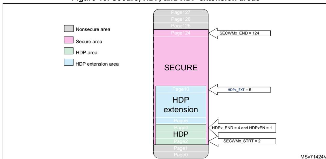
Other examples:
- • SECWM1_STRT = 0x6 and SECWM1_END = 0x7C
HDP1EN = 0xB4
HDP1_EXT = 0x6
There is no valid HDP area. Pages from 0x6 to 0x7C are secure. The pages from 0x6 to 0xB are protected by the HDP extension.
- • SECWM1_STRT = 0x6 and SECWM1_END = 0x10
HDP1_END = 0xB and HDP1EN ≠ 0xB4
HDP1_EXT = 0x9
Pages from 0x6 to 0xB (included) are protected by HDP. The pages from 0xC to 0x10 are protected by the HDP extension.
7.5.5 Block-based secure flash memory area protection
Any page can be programmed on-the-fly as secure or nonsecure using the block-based configuration registers. FLASH_SECB1Rx (resp. FLASH_SECB2Rx) are used to configure the security attribute for pages in bank 1 (resp. bank 2).
When the page security attribute (bit i in SECBByRx) is set, the security attribute is the same as the secure watermark-based area. The secure page is only accessible by a secure access.
If the SECBByRx[i] bit is set or reset for a page already included in a secure watermark-based area, the page keeps the watermark-based protection security attributes.
To modify a block-based page security attribution, the following actions are recommended:
- • Check that no flash memory operation is ongoing on the related page.
- • Add an ISB instruction after modifying the page security attribute bit i in SECByRx.
Caution: Switching a page or memory block from secure to nonsecure does not erase the content of the associated block. User secure software must perform the following needed operations before switching a block to nonsecure attribute:
- • Erase page content,
- • Invalidate the instruction cache.
Note: For SECByRx bit i access control, refer to Table 69 .
7.5.6 Flash security attribute state
The flash memory is secure when at least one secure area is defined either by watermark-based option bytes or block-based security registers.
It is possible to override the flash security state using the INV bit in FLASH_SCR.
FLASHEN and FLASHSMEN bits security attributes in the RCC follow the flash memory security attribute. It is possible to override the flash memory security attribute in the RCC using the INV bit in FLASH_SCR. A secure firmware setting this INV bit allows a nonsecure firmware to disable the flash memory clock when the flash memory is in power down or when the MCU enters low-power modes.
Table 53. Flash security state
| Secure area | INV bit | Flash security state |
|---|---|---|
| None | 0 | Nonsecure |
| 1 | Secure | |
| Yes | 0 | Secure |
| 1 | Nonsecure |
7.5.7 Block-based privileged flash memory area protection
Any page can be programmed on-the-fly as privileged or unprivileged using the block-based configuration registers. FLASH_PRIVBB1Rx (resp. FLASH_PRIVBB2Rx) are used to configure the privilege attribute for pages in bank 1 (resp. bank 2).
When the page privilege attribute (bit i in PRIVByRx) is set, the page is only accessible by a privileged access. An unprivileged page is accessible by a privileged or unprivileged access.
To modify a block-based privilege attribution, the following actions are recommended:
- • Check that no flash operation is ongoing on the related page.
- • Add an ISB instruction after modifying the page security attribute bit i in PRIVByRx.
Caution: Switching a page or memory block from privileged to unprivileged does not erase the content of the associated block.
Note: For PRIVByRx bit i access control, refer to Table 70 and Table 71 .
7.5.8 Flash memory register privileged and unprivileged modes
The flash memory registers can be read and written by privileged and unprivileged accesses, depending on the SPRIV and PRIV bits in FLASH_PRIVCFG, with the following rules:
- • When the SPRIV (resp. PRIV) bit is reset, all secure (resp. nonsecure) flash memory registers can be read and written by both privileged or unprivileged access.
- • When the SPRIV (resp. PRIV) bit is set, all secure (resp. nonsecure) flash memory registers can be read and written by privileged access only. Unprivileged access to a privileged registers is RAZ/WI.
Table 66 summarizes the flash memory registers access control.
7.5.9 Flash memory bank attributes in case of bank swap
The SWAP_BANK option bit modifies the address of each bank in the memory map. When SWAP_BANK is reset, the flash memory bank 1 is at the lower address range. When SWAP_BANK is set, the flash memory bank 1 is at the higher address range.
Flash memory bank attributes follow their bank so there is no need to modify the following registers when swapping banks:
- • FLASH secure watermark y register x FLASH_SECWMyRx
- • FLASH write protection x area y FLASH_WRPxyR (refer to Section 7.6.1 )
- • FLASH secure block based bank y register x FLASH_SECBByRx
- • FLASH privilege block based bank y register x FLASH_PRIVBByRx
- • PDREQx bits in FLASH_ACR
- • PDx bits in FLASH_SR
Note: The BK_ECC bit in FLASH_ECCCORR always refers to bank 1 (resp. bank 2) when it is low (resp. high), whatever SWAP_BANK value.
The BK_OP bit in FLASH_ECCDETR always refers to bank 1 (resp. bank 2) when it is low (resp. high), whatever SWAP_BANK value.
The figures below show how security attributes and protections behave in case of bank swap.
Figure 19. Flash memory security attributes and protections in case of no bank swap (SWAP_BANK = 0)
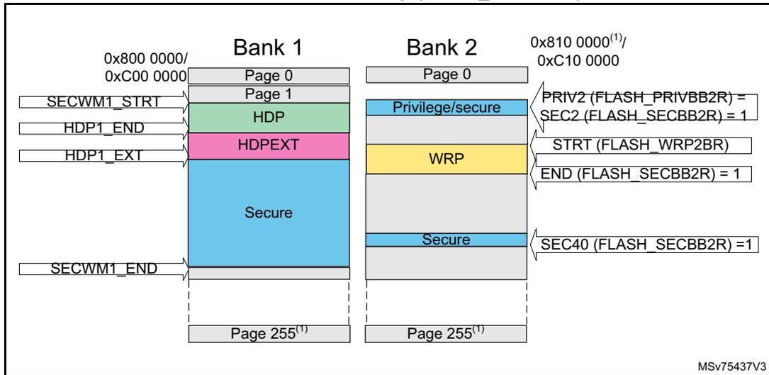
This diagram illustrates the flash memory layout for Bank 1 and Bank 2 when no bank swap is performed (SWAP_BANK = 0). Both banks start at address 0x800 0000. Bank 1 contains pages 0 to 255. Its security attributes are: SECWM1_STRT at the beginning, HDP (green) from page 1 to HDP1_END, HDPEXT (pink) from HDP1_END to HDP1_EXT, and a large Secure region (blue) from HDP1_EXT to SECWM1_END. Bank 2 also contains pages 0 to 255. Its security attributes are: Privilege/secure (light blue) for pages 0-1, WRP (yellow) for pages 2 to STRT(FLASH_WRP2BR), a gap until END(FLASH_SECB2R) = 1, and a Secure region (blue) from that point to the end of the bank. Register values for Bank 2 are: PRIV2(FLASH_PRIVBB2R) = SEC2(FLASH_SECB2R) = 1, STRT(FLASH_WRP2BR), END(FLASH_SECB2R) = 1, and SEC40(FLASH_SECB2R) = 1. A reference MSv75437V3 is noted at the bottom right.
1. Refer to Table 40 to Table 42 for Bank 2 base address and last page number.
Figure 20. Flash memory security attributes and protections in case of bank swap (SWAP_BANK = 1)
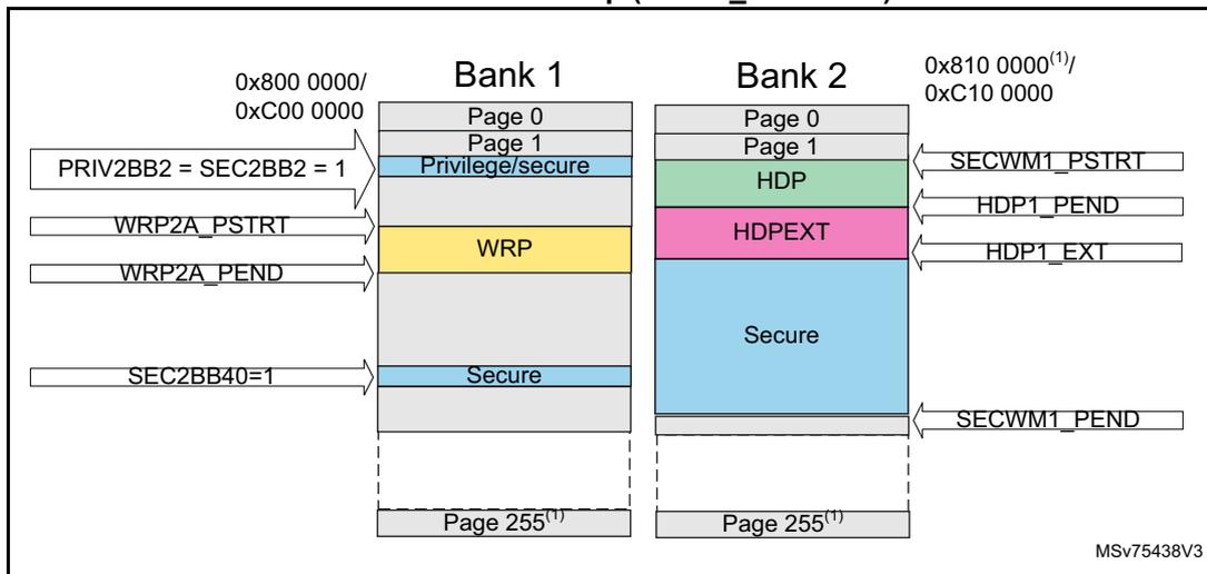
This diagram illustrates the flash memory layout for Bank 1 and Bank 2 when a bank swap is performed (SWAP_BANK = 1). Bank 1 (starting at 0x800 0000) now contains the security attributes originally for Bank 2: Privilege/secure (pages 0-1), WRP (yellow) from WRP2A_PSTRT to WRP2A_PEND, and a Secure region (blue) starting at SEC2BB40=1. Bank 2 (starting at 0x810 0000) contains the security attributes originally for Bank 1: HDP (green) from SECWM1_PSTRT to HDP1_PEND, HDPEXT (pink) from HDP1_PEND to HDP1_EXT, and a Secure region (blue) from HDP1_EXT to SECWM1_PEND. Register values for Bank 1 are: PRIV2BB2 = SEC2BB2 = 1, WRP2A_PSTRT, WRP2A_PEND, and SEC2BB40=1. A reference MSv75438V3 is noted at the bottom right.
1. Refer to Table 40 to Table 42 for Bank 2 base address and last page number.
7.6 FLASH memory protection
The flash memory interface implements the following protection mechanisms:
- • Write protection (WRP)
- • Readout protection (RDP)
- • Additional secure protections when TrustZone is active (refer to
Section 7.5
)
- – Up to two secure watermark-based nonvolatile areas
- – Up to two secure hide protection areas
- – Secure block-based volatile areas with page granularity
- • Privileged block-based volatile areas with page granularity (refer to Section 7.5.7 )
7.6.1 Write protection (WRP)
The user area in the flash memory can be protected against unwanted write operations. Two write-protected (WRP) areas can be defined in each bank, with page granularity.
Each area is defined by a start page offset and an end page offset related to the physical flash bank base address. These offsets are defined in the WRP address registers: FLASH_WRP1AR, FLASH_WRP1BR, FLASH_WRP2AR, and FLASH_WRP2BR.
The bank "x" WRP "y" area (x = 1,2 and y = A,B) is defined as follows:
- • From the address: bank "x" base address + [FLASH_WRPxyR[STRT] × 0x1000] (included)
- • To the address: bank "x" base address + [(FLASH_WRPxyR[END]+1) × 0x1000] (excluded)
For example, to protect by WRP from the address 0x0806 2000 (included) to the address 0x0807 3FFF (included):
- • If the banks are not swapped, FLASH_WRP1AR must be programmed with:
- – STRT = 0x62
- – END = 0x73
- • If the two banks are swapped, the protection must apply to bank 2, and FLASH_WRP2AR must be programmed with:
- – STRT = 0x62
- – END = 0x73
Note: For more details on the bank swapping mechanism, refer to Section 7.5.9 .
When WRP is active, protected flash memory pages cannot be erased or programmed. Consequently, a software mass erase cannot be performed if one area is write-protected.
If an erase/program operation to a write-protected part of the flash memory is attempted, the secure or nonsecure write protection error flag (WRPERR) is set in FLASH_SR or FLASH_SSR. This flag is also set for any write access to the following:
- • System flash memory
- • OTP area
Note: When the memory readout protection level 1 is selected (RDP level = 1), it is not possible to program or erase the flash memory (secure or nonsecure) if the CPU debug features are
connected (JTAG or single wire) or boot code is being executed from RAM or system flash memory, even if WRP is not activated.
When the memory readout protection level 0.5 is selected (RDP level = 0.5), it is not possible to program or erase the flash secure memory if the CPU debug features are connected (JTAG or single wire), even if WRP is not activated.
To validate the WRP options, the option bytes must be reloaded through the OBL_LAUNCH bit in the flash control register.
Table 54. WRP protection
| WRP registers values (x = 1/2 y = A/B) | WRP area |
|---|---|
| FLASH_WRPxy[STRT] = FLASH_WRPxy[END] | Page WRPxy is protected. |
| FLASH_WRPxy[STRT] > FLASH_WRPxy[END] | No WRP area |
| FLASH_WRPxy[STRT] < FLASH_WRPxy[END] | The pages from FLASH_WRPxy[STRT] to FLASH_WRPxy[END] are protected. |
Write protection lock
Each WRP area can be independently locked by writing 0 to the UNLOCK bit in FLASH_WRP1AR, FLASH_WRP1BR, FLASH_WRP2AR, or FLASH_WRP2BR. Once a WRP area is locked, it is not possible to modify its settings. In order to unlock a WRP area, a regression to RDP level 0 must be launched.
In order to make the WRP area immutable and act as a ROM, the following actions are needed:
- • If RDP level is 0, 0.5 or 1, provision a OEM1KEY in order to prevent a regression to RDP level 0 for users not knowing the key.
- • If RDP level is 2, either provision a OEM1KEY (refer to first bullet) or do not provision a OEM2KEY (preventing regression from level 2 to level 1).
For more information on RDP regressions, refer to Device life cycle managed by readout protection (RDP) transitions .
7.6.2 Readout protection (RDP)
The readout protection protects the flash main memory, the option bytes, the backup registers, and the SRAMs. In order to reach the best protection level, it is recommended to activate TrustZone, and to set the RDP level 2 with password authentication regression enabled (refer to Readout protection levels when TrustZone is enabled ).
Readout protection levels when TrustZone is disabled
There are three levels of readout protection from no protection (level 0) to maximum protection or no debug (level 2).
The flash memory is protected according to the RDP option-byte value shown in the table below.
Table 55. Flash memory readout protection status (TZEN = 0)
| RDP byte value | Readout protection level |
|---|---|
| 0xAA | Level 0 |
| Any value except 0xAA or 0xCC | Level 1 |
| 0xCC | Level 2 |
- • Level 0: no protection
Read, program and erase operations into the flash main memory area are possible. Option bytes, SRAMs, and backup registers are also accessible by all operations.
- • Level 1: readout protection
When the readout protection level 1 is set:
- – User mode: code executing in user mode (boot flash) can access the flash main memory, option bytes, SRAMs, and backup registers with all operations (read, erase, program).
- – Debug, boot RAM, and bootloader modes: in debug mode or when the microcontroller boots from RAM or system memory, the flash main memory, the backup registers, and the SRAM2 are totally inaccessible. Any read or write access to the flash main memory generates a bus error and a hard fault interrupt.
- • Level 2: no debug
When the readout protection level 2 is set:
- – The protection level 1 is guaranteed.
- – All debug features are disabled:
- - if OEM2 key has not been provided, JTAG and SWD are definitively disabled.
- - if OEM2 key has been provided under a lower RDP protection, JTAG and SWD remain enabled under reset only to interface with DBGMCU_SR, DBGMCU_DBG_AUTH_HOST, and DBGMCU_DBG_AUTH_DEVICE registers to obtain device identification and provide OEM2 key to request RDP regression.
- – The boot from SRAM (boot RAM mode) and the boot from system memory (bootloader mode) are no longer available.
- – Only boot from main flash memory is possible; all operations are allowed on the flash main memory. Read, erase and program accesses to the flash memory and SRAMs from user code are allowed.
- – Option bytes cannot be programmed nor erased except the SWAP_BANK option bit. Thus, the level 2 cannot be removed: it is an irreversible operation unless an OEM2 key has been provisioned (refer to OEM2 RDP lock mechanism ).
Note: The debug feature is also disabled under reset.
STMicroelectronics is not able to perform analysis on defective parts on which the level 2 protection has been set. Regress parts to RDP level 1 before returning them for analysis (refer to OEM2 RDP lock mechanism ).
Table 56. Access status versus protection level and execution mode when TZEN = 0| Area | RDP level | User execution (boot from flash) | Debug/boot from RAM/ bootloader (1) | ||||
|---|---|---|---|---|---|---|---|
| Read | Write | Erase | Read | Write | Erase | ||
| Flash main memory | 1 | Yes | Yes | Yes | No | No | No (2) |
| 2 | Yes | Yes | Yes | N/A | N/A | N/A | |
| System memory (3) | 1 | Yes | No | No | Yes | No | No |
| 2 | Yes | No | No | N/A | N/A | N/A | |
| Option bytes (4) | 1 | Yes | Yes (2) | N/A | Yes | Yes | N/A |
| 2 | Yes | No (5) | N/A | N/A | N/A | N/A | |
| OTP | 1 | Yes | Yes (6) | N/A | Yes | Yes (6) | N/A |
| 2 | Yes | Yes (6) | N/A | N/A | N/A | N/A | |
| Backup registers | 1 | Yes | Yes | N/A | No | No | N/A (7) |
| 2 | Yes | Yes | N/A | N/A | N/A | N/A | |
| SRAM2 | 1 | Yes | Yes | N/A | No | No | N/A (8) |
| 2 | Yes | Yes | N/A | N/A | N/A | N/A | |
- 1. When the protection level 2 is active, the debug port, the boot from RAM and the boot from system memory are disabled.
- 2. The system memory is only read-accessible, whatever the protection level (0, 1 or 2) and execution mode.
- 3. The system memory is only read-accessible, whatever the protection level (0, 1 or 2) and execution mode.
- 4. Option bytes are only accessible through the flash registers interface and OPTSTRT bit.
- 5. SWAP_BANK option bit can be modified.
- 6. OTP can only be written once.
- 7. The backup registers are erased when RDP changes from level 1 to level 0.
- 8. All SRAMs are erased when RDP changes from level 1 to level 0. On STM32U3B5/3C5 devices, SRAM4 is not erased on RDP regression.
Readout protection levels when TrustZone is enabled
There are four levels of readout protection from no protection (level 0) to maximum protection or no debug (level 2). The flash memory is protected according to the RDP option-byte value shown in the table below.
Table 57. Flash memory readout protection status (TZEN = 1)| RDP byte value | Readout protection level |
|---|---|
| 0xAA | Level 0 |
| 0x55 | Level 0.5 |
| Any value except 0xAA or 0x55 or 0xCC | Level 1 |
| 0xCC | Level 2 |
- • Level 0: no protection
Read, program and erase operations into the flash main memory area are possible. The option bytes, the SRAMs and the backup registers are also accessible by all operations.
- – RSS mode: when booting from RSS, the debug access is disabled while executing RSS code.
- • Level 0.5: nonsecure debug only
All read and write operations (if no write protection is set) from/to the nonsecure flash memory are possible. The debug access to secure area is prohibited. Debug access to nonsecure area remains possible.
- – User mode: code executing in user mode (boot flash) can access the flash main memory, option bytes, SRAMs and backup registers with all operations (read, erase, program).
- – Nonsecure debug mode: nonsecure debug is possible when the CPU is in nonsecure state. The secure flash memory, secure backup registers, and SRAMs are inaccessible. The nonsecure flash memory, nonsecure backup registers, and nonsecure SRAMs remain accessible for debug purpose.
- – RSS mode: when booting from RSS, the debug access is disabled while executing RSS code.
- – Boot RAM mode: boot from SRAM is not possible.
- • Level 1: readout protection
When the readout protection level 1 is set:
- – User mode: code executing in user mode (boot flash) can access the flash main memory, option bytes, SRAMs and backup registers with all operations (read, erase, program).
- – Nonsecure debug mode: nonsecure debug is possible when the CPU is in nonsecure state. However, an intrusion is detected in case of debug access: the flash main memory, backup registers, and the SRAM2 are totally inaccessible. Any read or write access to the flash main memory generates a bus error and a hard fault interrupt.
- – RSS mode: when booting from RSS, the debug access is disabled while executing RSS code.
- – Boot RAM mode: boot from SRAM is not possible.
- • Level 2: no debug
When the readout protection level 2 is set:
- – The protection level 1 is guaranteed.
- – All debug features are disabled
- -if OEM2 key has not been provided, JTAG and SWD are definitively disabled.
- – -if OEM2 key has been provided under a lower RDP protection, JTAG and SWD remain enabled under reset only to interface with DBGMCU_SR, DBGMCU_DBG_AUTH_HOST, and DBGMCU_DBG_AUTH_DEVICE registers to obtain device identification and provide OEM2 key to request RDP regression.
- – The boot from SRAM (boot RAM mode) and the boot from system memory (boot loader mode) are no longer available.
- – Boot from RSS is possible.
- – When booting from main flash or RSS, all operations are allowed on the flash main memory. Read, erase and program accesses to flash memory and SRAMs from user code are allowed.
- – Option bytes cannot be programmed nor erased except the SWAP_BANK option bit. Thus, the level 2 cannot be removed: it is an irreversible operation unless an OEM2 key has been provisioned (refer to OEM2 RDP lock mechanism ).
Note: The debug feature is also disabled under reset.
STMicroelectronics is not able to perform analysis on defective parts on which the level 2 protection has been set. Regress parts to RDP level 1 before returning them for analysis (refer to OEM2 RDP lock mechanism ).
Table 58. Access status versus protection level and execution modes when TZEN = 1
| Area | RDP level | User execution (boot from flash) | Debug/bootloader (1) | ||||
|---|---|---|---|---|---|---|---|
| Read | Write | Erase | Read | Write | Erase | ||
| Flash main memory | 0.5 | Yes | Yes | Yes | Yes (2) | Yes (2) | Yes (2) |
| 1 | Yes | Yes | Yes | No | No | No (5) | |
| 2 | Yes | Yes | Yes | N/A | N/A | N/A | |
| System memory (3) | 0.5 | Yes | No | No | Yes | No | No |
| 1 | Yes | No | No | Yes | No | No | |
| 2 | Yes | No | No | N/A | N/A | N/A | |
| Option bytes (4) | 0.5 | Yes | Yes (5) | N/A | Yes | Yes (5) | N/A |
| 1 | Yes | Yes (5) | N/A | Yes | Yes (5) | N/A | |
| 2 | Yes | No (6) | N/A | N/A | N/A | N/A | |
| OTP | 0.5 | Yes | Yes (7) | N/A | Yes | Yes (7) | N/A |
| 1 | Yes | Yes (7) | N/A | Yes | Yes (7) | N/A | |
| 2 | Yes | Yes (7) | N/A | N/A | N/A | N/A | |
| Backup registers | 0.5 | Yes | Yes | N/A | Yes (2) | Yes (2) | N/A (8) |
| 1 | Yes | Yes | N/A | No | No | N/A (8) | |
| 2 | Yes | Yes | N/A | N/A | N/A | N/A | |
| SRAM2 | 0.5 | Yes | Yes | N/A | Yes (2) | Yes (2) | N/A (9) |
| 1 | Yes | Yes | N/A | No | No | N/A (9) | |
| 2 | Yes | Yes | N/A | N/A | N/A | N/A | |
1. When the protection level 2 is active, the debug port and the bootloader mode are disabled.
2. Depends on TrustZone security access rights.
3. The system memory is only read-accessible, whatever the protection level (0, 1 or 2) and execution mode.
4. Option bytes are only accessible through the flash registers interface and OPTSTRT bit.
5. The flash main memory is erased when the RDP option byte regresses from level 1 to level 0.
6. SWAP_BANK option bit can be modified.
7. OTP can only be written once.
- 8. The backup registers are erased when RDP changes from level 1 to level 0 and when RDP changes from level 1 to level 0.5.
- 9. All SRAMs except SRAM4 are erased when RDP changes from level 1 to level 0 and when RDP changes from level 1 to level 0.5.
Device life cycle managed by readout protection (RDP) transitions
It is easy to move from level 0 or level 0.5 to level 1 by changing the value of the RDP byte to any value (except 0xCC). By programming the 0xCC value in the RDP byte, it is possible to go to level 2 either directly from level 0 or from level 0.5 or from level 1. Once in level 2, it is no longer possible to modify the readout protection level unless an OEM2 key is provisioned (refer to OEM2 RDP lock mechanism ).
When the RDP is reprogrammed to the value 0xAA to move from level 1 to level 0, a mass erase of the flash main memory and all SRAMs is performed except for SRAM4. Backup registers, ICACHE, and PKA SRAM are also erased. The OTP area is not erased.
At RDP level 0.5, it is not possible to request RDP level 0. Instead, a RDP increase to level 1 followed by a RDP regression to level 0 is required.
When the RDP is programmed to the value 0x55 to move from level 1 to level 0.5, a partial mass erase of the flash main memory is performed. Only nonsecure watermark-based areas are erased (even if it is defined as secure by block-based). Backup registers, ICACHE, PKA SRAM, and all SRAMs are mass erased except for SRAM4. The OTP area is not erased. The RDP level 0.5 and partial nonsecure erase are only available when TrustZone is active.
Caution: On STM32U3B5/3C5 devices, SRAM4 is not erased on RDP regression. The user must make sure no sensitive data is stored in SRAM4.
Note: Full mass erase is performed only when level 1 is active and level 0 requested. When the protection level is increased (0 to 0.5, 0 to 1, 0.5 to 1, 1 to 2, 0 to 2 or 0.5 to 2), there is no mass erase.
To validate the readout protection level change, the option bytes must be reloaded through the OBL_LAUNCH bit in FLASH_CR.
Before launching a RDP regression, the software must invalidate the ICACHE and wait for the BUSYF bit to be cleared.
Figure 21. RDP level transition scheme when TrustZone is disabled (TZEN = 0)
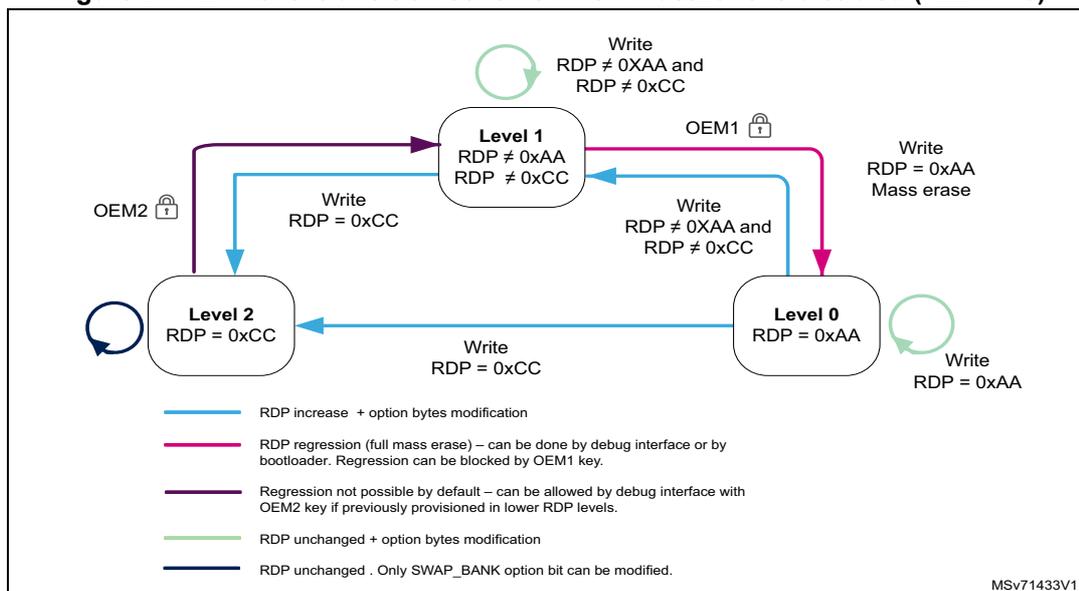
Figure 22. RDP level transition scheme when TrustZone is enabled (TZEN = 1)
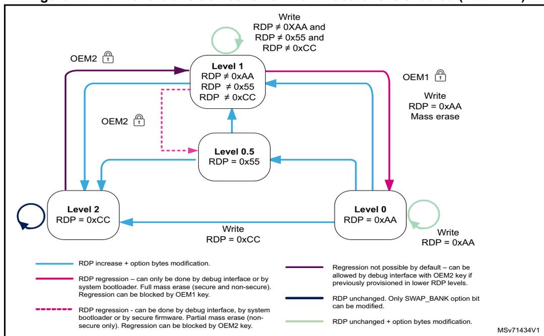
OEM1/OEM2 lock activation
Two 128-bit keys (OEM1KEY and OEM2KEY) can be defined in order to lock the RDP regression. Each 128-bit key is coded on four registers:
- • OEM1KEY coded on FLASH_OEM1KEYRx (x = 1 to 4)
- • OEM2KEY coded on FLASH_OEM2KEYRx (x = 1 to 4).
OEM1KEY and OEM2KEY cannot be read through these registers but there are two 8-bit CRC (OEM1KEYCRC and OEM2KEYCRC), which can be used as a public key information.
Any read access to OEM1KEY and OEM2KEY returns zero.
OEM1KEY can be modified:
- • In readout protection level 0
- • In readout protection level 0.5 or 1 if OEM1LOCK = 0 in FLASH_SR
OEM2KEY can be modified:
- • In readout protection level 0 or 0.5
- • In readout protection level 1 if OEM2LOCK = 0 in FLASH_SR
When attempting to modify FLASH_OEM1KEYRx or FLASH_OEM2KEYRx without following these rules, the user option modification is not done and the OPTWERR bit is set.
In order to activate OEM1 lock mechanism, the following steps are needed:
- 1. Check that the OEM1LOCK bit is not set or that the readout protection is at level 0.
- 2. Write a 128-bit key in FLASH_OEM1KEYRx
- 3. Check key CRC thanks to OEM1KEYCRC.
- 4. Launch option modification by setting the OPTSTRT bit in FLASH_CR.
- 5. Wait for the BSY bit to be cleared and check that OPTWERR is not set.
- 6. Set the OBL_LAUNCH option bit to start option-byte loading or perform a power-on reset.
- 7. Check that OEM1LOCK is set.
In order to activate OEM2 lock mechanism, the following steps are needed:
- 1. Check that the OEM2LOCK bit is not set or that the readout protection is at level 0 or 0.5.
- 2. Write a 128-bit key in FLASH_OEM2KEYRx.
- 3. Check key CRC using OEM2KEYCRC.
- 4. Launch option modification by setting the OPTSTRT bit in FLASH_CR.
- 5. Wait for the BSY bit to be cleared and check that OPTWERR is not set.
- 6. Set the OBL_LAUNCH option bit to start option-byte loading or perform a power-on reset.
- 7. Check that OEM2LOCK is set.
Note: The OEM1KEY and OEM2KEY must contain more than four 0.
It is recommended to always activate OEM2 lock mechanism even if no regression level is expected.
Once set, the RDP transition with OEM keys mechanism cannot be disabled. This means that the OEM keys can be modified, but never cleared.
OEM1 RDP lock mechanism
The OEM1 RDP lock mechanism is active when the OEM1LOCK bit is set. It blocks the RDP level 1 to RDP level 0 regression.
In order to regress from RDP level 1 to RDP level 0, the following unlock sequence must be applied:
- 1. Shift OEM1KEY[31:0], OEM1KEY[63:32], OEM1KEY[95:64] and then OEM1KEY[127:96] through JTAG or SWD in DBGMCU_DBG_AUTH_HOST.
- 2. If this key matches the OEM1KEY value, the RDP regression can be launched by setting the OPTSTRT bit.
- 3. If the key does not match the OEM1KEY value, the RDP regression and any access to the flash memory are blocked until a next power-on reset.
Attempting to regress from RDP level 1 to RDP level 0 without following this sequence sets the OPTWERR option bit and the option bytes remain unchanged.
When the lock mechanism is not activated (OEM1LOCK = 0), the regression from RDP level 1 to RDP level 0 is always granted.
OEM2 RDP lock mechanism
The OEM2 RDP lock mechanism is active when the OEM2LOCK bit is set. It allows the following actions:
- • Block RDP level 1 to RDP level 0.5 regression.
- • Authorize RDP level 2 to RDP level 1 regression.
In order to regress from RDP level 1 to RDP level 0.5, the following unlock sequence must be applied:
- 1. Shift OEM2KEY[31:0], OEM2KEY[63:32], OEM2KEY[95:64], and then OEM2KEY[127:96] through JTAG or SWD under reset in DBGMCU_DBG_AUTH_HOST.
- 2. Release reset if this key matches the OEM2KEY value, the RDP regression can be launched by setting the OPTSTRT bit.
- 3. If the key does not match the OEM2KEY value, the RDP regression and any access to the flash memory are blocked until a next power-on reset to reload option bytes.
In order to regress from RDP level 2 to RDP level 1, the following unlock sequence must be applied:
- 1. Shift OEM2KEY[31:0], OEM2KEY[63:32], OEM2KEY[95:64], and then OEM2KEY[127:96] through JTAG or SWD under reset in DBGMCU_DBG_AUTH_HOST register
- 2. Release reset if this key matches the OEM2KEY value:
- – The RDP regression is launched by hardware (it is not possible to execute instructions when the key is matching).
- – Apply a power-on reset (cycle V DD power supply OFF and ON).
- 3. If the key does not match the OEM2KEY value, the RDP regression and any access to the flash memory are blocked until a next power-on reset to reload option bytes.
Attempting to regress from RDP level 2 to RDP level 1 without following these sequences, leaves option bytes unchanged.
Attempting to regress from RDP level 1 to RDP level 0.5 without following these sequences, sets the OPTWERR option bit and the option bytes remain unchanged.
When the lock mechanism is not activated (OEM2LOCK = 0), the following happens:
- • The regression from RDP level 1 to RDP level 0.5 is always granted.
- • The regression from RDP level 2 to RDP level 1 is never granted. When attempting to modify the options bytes, the protection error flag OPTWERR is set in FLASH_SR, and an interrupt can be generated.
OEM Key CRC source
Below is the CRC source code that can be used to compare with the result of the computation provided by the flash interface in OEM1KEYCRC (resp. OEM2KEYCRC) bitfield after loading the keys in FLASH OEM1 (resp. OEM2) Key registers.
uint8_t getCRC(uint32_t * keyin)
{
    const uint8_t CRC7_POLY = 0x7;
    const uint32_t key_strobe[4] = {0xAA55AA55, 0x3, 0x18, 0xC0}; uint8_t i, j, k, crc = 0x0;
    uint32_t keyval;
    for (j = 0; j < 4; j++)
    {
        keyval = *(keyin+j);
        if (j == 0) { keyval ^= key_strobe[0]; }
        else { keyval ^= (key_strobe[j] << 24) | (crc << 16) | (key_strobe[j] << 8) | crc; }
        for (i = 0, crc = 0; i < 32; i++)
        {
            k = (((crc >> 7) ^ (keyval >> (31-i))&0xF)) & 1; crc <<= 1;
            if (k) { crc ^= CRC7_POLY; }
        }
        crc ^= 0x55;
    }
    return crc;
}
7.7 System memory
System memory stores RSS (root secure services) firmware programmed by STMicroelectronics during production. RSS provides runtime services to user firmware. When TrustZone® is enabled (user sets the TZEN bitfield to 1), RSS provides secure services to the secure user firmware only. When TrustZone® is disabled (user sets the TZEN bitfield to 0), RSS does not provide nonsecure services to the user firmware.
7.7.1 RSS user functions
The RSS provides runtime services using the RSS library, whose functions are exposed to the user within the CMSIS device header file, provided by the STM32Cube firmware package.
RSS provides services through the RSSLIB library, dedicated to secure user firmware when the system is configured with TrustZone® enabled (TZEN bitfield set to 1).
Table 59. Macros for RSS services
| TrustZone | C defined macro | Location in flash memory |
|---|---|---|
| Enabled | RSSLIB_PFUNC | 0x0BF99040 |
| Disabled | NA | NA |
RSSLIB
The secure user firmware calls the RSSLIB functions using RSSLIB_PFUNC C-defined macro, which points to a location within the nonsecure system memory. Before calling the RSSLIB functions, the secure user firmware must define a nonsecure region above this location within SAU of the Cortex®-M33 processor, starting from RSSLIB_SYS_FLASH_NS_PFUNC_START (0x0BF99040), up to
RSSLIB_SYS_FLASH_NS_PFUNC_END (0x0BF990FF). These last addresses are provided within the CMSIS device header file.
The user can configure this nonsecure region either by using the CMSIS system partition header file, or by implementing their own code for SAU setup. The CMSIS system partition header file is part of the STM32Cube firmware package.
Table 60. RSS lib interface functions
| Library | Function | Attributes |
|---|---|---|
| RSSLIB_PFUNC | CloseExitHDP | Secure callable function |
| CloseExitHDPEExt |
CloseExitHDP
Secure attribute:
- • secure callable function
Prototype:
- •
uint32_t CloseExitHDP (uint32_t HdpArea, uint32_t VectorTableAddr);
Arguments:
- • HdpArea: notifies which hdp area to close, can be a combination of hdp area 1 and hdp area 2
- • VectorTableAddr: a pointer on the vector table containing the reset handler the function jumps to
Returned values:
- • 0xF5F5F5F5U: error on input parameter
- • otherwise, does not return
CloseExitHDP closes the requested hdp area passed in input parameter and jumps to the reset handler present within the vector table. The function does not return on successful execution.
CloseExitHDPEExt
Secure attribute:
- • secure callable function
Prototype:
- •
uint32_t CloseExitHDPEExt (uint32_t HdpExtArea, uint32_t VectorTableAddr, uint32_t CloseBound);
Arguments:
- • HdpExtArea: notifies which hdp extension area to close, can be a combination of hdp extension area 1 and hdp extension area 2
- • VectorTableAddr: pointer on the vector table containing the reset handler the function jumps to
- • CloseBound: notifies if the HDP extension area should be closed with HDPx_EXT increment allowed or not
Returned values:
- • 0xF5F5F5F5U: error on input parameter
- • Otherwise, does not return
CloseExitHDPExt closes the requested hdp extension area passed in input parameter and jumps to the reset handler present within the vector table. The function does not return on successful execution.
7.8 Summary of flash memory and flash memory registers access control
The flash interface evaluates the access restrictions in the following orders: RDP level, TrustZone security, write protection (for write access), HDP, and privilege. The tables below summarize all the flash memory and registers accesses status versus RDP level, WRP and HDP protections.
Table 61. Flash memory access versus RDP level when TrustZone is active (TZEN = 1)
| Access type | RDP level 0, RDP level 0.5, RDP level 1 no intrusion (1) , or RDP level 2 | RDP level 1 with intrusion (2) | ||
|---|---|---|---|---|
| Nonsecure page | Secure page | Nonsecure or secure page | ||
| Secure | Fetch | Bus error | OK | Bus error |
| Read | RAZ, flash illegal access event | |||
| Write | WI, secure WRPERR flag set, flash illegal access event | No WRP: OK | WI, secure WRPERR flag set | |
| Page erase | WRP pages: WI and secure WRPERR flag set | WRP pages: WI and secure WRPERR flag set | ||
| Nonsecure | Fetch | OK | Bus error | Bus error |
| Read | RAZ, flash illegal access event | |||
| Write | No WRP: OK | WI, non secure WRPERR flag set, flash illegal access event | WI, nonsecure WRPERR flag set | |
| Page erase | WRP pages: WI and nonsecure WRPERR flag set | |||
- 1. RDP level 1 no intrusion = when booting from user flash memory and no debug access.
- 2. RDP level 1 with intrusion = when debug access detected.
Table 62. Flash memory access versus HDPx and HDPx extended (x = 1 or 2)
| Access type | Flash memory area | |||
|---|---|---|---|---|
| HDPx (with x = 1,2) | HDP1Ext | HDP2Ext | Others | |
| fetch | OK if HDPx is open (1) else RAZ | OK if HDP1Ext is open (2) and HDP1 and HDP2 closed or not defined, else RAZ | OK if HDP2Ext is open and HDP1 and HDP2 closed or not defined, else RAZ | OK if HDP1, HDP2, HDP1Ext and HDP2Ext are closed or not defined, else RAZ |
Table 62. Flash memory access versus HDPx and HDPx extended (x = 1 or 2) (continued)
| Access type | Flash memory area | |||
|---|---|---|---|---|
| HDPx (with x = 1,2) | HDP1Ext | HDP2Ext | Others | |
| Read | OK if HDPx is open, else RAZ | OK if HDP1Ext is open, else RAZ | OK if HDP2Ext is open, else RAZ | OK |
| Write/ page erase | OK if HDPx open, else WI, secure WRPERR flag set | OK if HDP1Ext is open, else WI, secure WRPERR flag set | OK if HDP2Ext is open, else WI, secure WRPERR flag set | OK |
- 1. "HDPx area is open" means that HDPx_ACCDIS = HDPxEXT_ACCDIS = 0xA3. Otherwise, it is closed. "HDPx area is defined" is described in Table 50 .
- 2. "HDPxExt is open" means that HDPxEXT_ACCDIS = 0xA3. Otherwise, it is closed. When HDPxExt is closed (HDPxEXT_ACCDIS \( \neq \) 0xA3), HDPx is automatically closed. "HDPxExt area is not defined" is described in Table 52 .
Table 63. Flash memory access versus RDP level when TrustZone is disabled (TZEN = 0)
| Access type | RDP level 0, RDP level 1 no intrusion, or RDP level 2 (1) | RDP level 1 with intrusion (2) |
|---|---|---|
| Fetch | OK | Bus error |
| Read | ||
| Write | No WRP: OK | WI and nonsecure WRPERR flag set |
| Erase | WRP pages: WI and nonsecure WRPERR flag set |
- 1. RDP level 1 no intrusion = when booting from user flash memory and no debug access.
- 2. RDP level 1 with intrusion = when booting from RAM or system memory or debug access detected.
Table 64. Flash memory mass erase versus RDP level when TrustZone is active (TZEN = 1)
| Access type | RDP level 0, RDP level 0.5, RDP level 1 no intrusion or RDP level 2 (1) | RDP level 1 with intrusion (2) | |||||
|---|---|---|---|---|---|---|---|
| Nonsecure flash memory | Secure flash memory | Mix nonsecure and secure flash memory | |||||
| HDP area (HDPxEN \( \neq \) 0xB4 HDPx_ ACCDIS \( \neq \) 0xA3) | HDP extension area (HDPxEXT_ ACCDIS \( \neq \) 0xA3) | Others (3) | |||||
| Secure | Bank or mass erase | WI, secure WRPERR flag set, flash memory illegal access event | WI, secure WRPERR flag set | WI, secure WRPERR flag set | No WRP: OK WRP pages: WI and secure WRPERR flag set | WI, secure WRPERR flag set, flash memory illegal access event | WI, secure WRPERR flag set |
| Non secure | Bank or mass erase | No WRP: OK WRP pages: WI and nonsecure WRPERR flag set | WI, nonsecure WRPERR flag set, flash memory illegal access event | WI, nonsecure WRPERR flag set | |||
- 1. RDP level 1 no intrusion = when booting from user flash memory and no debug access.
- RDP level 1 with intrusion = when debug access detected.
- “Others” refers to the other flash memory secure configurations than the one described for HDP protections or for HDP extension protection. Example: flash memory secure and HDPx area enabled but HDPx_ACCDIS = 0xA3, or flash memory secure and HDPx extension area defined but HDPxEXT_ACCDIS = 0xA3.
| Access type | System memory (bootloader) | OTP | RSS | |
|---|---|---|---|---|
| Secure (TZEN = 1) | Fetch | Bus error | RAZ | |
| Read | RAZ, flash memory register illegal access event | OK | ||
| Write | WI, secure WRPERR flag set, flash memory illegal access event | |||
| Nonsecure (TZEN = 0 or TZEN = 1) | Fetch | OK | Bus error | Bus error |
| Read | OK | RAZ (1) | ||
| Write | WI and nonsecure WRPERR flag set | OK if not virgin: WI, nonsecure PROGERR flag set | WI, nonsecure WRPERR flag set | |
- Flash memory illegal access event is generated when TZEN = 1.
| Access type | Nonsecure register | Secure register | ||||
|---|---|---|---|---|---|---|
| PRIV = 1 | PRIV = 0 | SPRIV = 1 | SPRIV = 0 | |||
| Fetch | Secure/ nonsecure | Privileged/ unprivileged | Bus error | |||
| Read/ Write | Secure (2) | Privileged | OK | |||
| Unprivileged | RAZ/WI | OK | RAZ/WI | OK | ||
| Nonsecure (3) | Privileged | OK | RAZ/WI and a flash memory register illegal access event (4) | |||
| Unprivileged | RAZ/WI | OK | ||||
- Except FLASH_SECBByRx, FLASH_PRIVBByRx, and FLASH_PRIVCFGGR.
- Secure access is only valid when TrustZone is active (TZEN = 1).
- Nonsecure access are valid when TrustZone is active or disabled.
- Flash register illegal access event is only generated when TZEN = 1.
| Access type | Unprivileged page | Privileged page | |
|---|---|---|---|
| Fetch, read/write, page erase | Privileged | OK | |
| Fetch, read | Unprivileged | OK | RAZ |
| Write, page erase | Unprivileged | WI, secure or nonsecure WRPERR flag set | |
- When TZEN = 1, access must be granted by security firewall before privilege is considered
| Access type | Unprivileged flash memory | Privileged flash memory | Mix unprivileged and privileged flash memory | |
|---|---|---|---|---|
| Mass erase | Privileged | OK | ||
| Mass erase | Unprivileged | OK | WI, secure or nonsecure WRPERR flag set | |
1. When TZEN = 1, access must be granted by security firewall before privilege is considered
Table 69. FLASH_SECBByRx registers access when TrustZone is active (TZEN = 1)| Access type | Bit i in FLASH_SECBByRx | Bit i in FLASH_SECBByRx | ||
|---|---|---|---|---|
| Fetch | Secure/nonsecure | Privileged/unprivileged | - | Bus error |
| Read | Secure/nonsecure | Privileged/unprivileged | - | OK |
| Write | Secure | Privileged | - | OK |
| Unprivileged | 0 | OK for bit i | ||
| Nonsecure | Privileged/unprivileged | - | WI and a flash memory register illegal access event | |
| Access type | Page secure state (watermark or blocked based) | Bit i in FLASH_PRIVBByRx | ||
|---|---|---|---|---|
| Fetch | Privileged/unprivileged | Secure/nonsecure | - | Bus error |
| Read | Privileged/unprivileged | Secure/nonsecure | - | OK for all bits |
| Write | Privileged | Secured | - | OK for all bits |
| Nonsecure | Nonsecure | OK for bit i | ||
| Unprivileged | Nonsecure | Secure | WI for bit i | |
| Secured/nonsecure | - | WI for all bits | ||
| Access type | FLASH_PRIVBByRx | |
|---|---|---|
| Fetch | Privileged/unprivileged | Bus error |
| Read | Privileged/unprivileged | OK |
| Write | Privileged | OK |
| Unprivileged | WI | |
7.9 FLASH interrupts
Table 72. Flash interrupt requests
| Interrupt vector | Interrupt event | Event flag | Event flag/interrupt clearing method | Interrupt enable control bit | Exit Sleep mode | Exit Stop and Standby modes |
|---|---|---|---|---|---|---|
| FLASH_S | Secure end of operation | Secure EOP (1) | Write secure EOP = 1 | Secure EOPIE | Yes | No |
| Secure operation error | Secure OPERR (2) | Write secure OPERR = 1 | Secure ERRIE | Yes | No | |
| FLASH | Nonsecure end of operation | Nonsecure EOP (1) | Write nonsecure EOP = 1 | Nonsecure EOPIE | Yes | No |
| Nonsecure operation error | Nonsecure OPERR (2) | Write nonsecure OPERR = 1 | Nonsecure ERRIE | Yes | No | |
| ECC correction | ECCC | Write ECCC = 1 | ECCIE | Yes | No |
- Secure EOP (resp. nonsecure EOP) is set only if secure EOPIE (resp. nonsecure EOPIE) is set.
- Secure OPERR (resp. nonsecure OPERR) is set only if secure ERRIE (resp. nonsecure ERRIE) is set.
7.10 FLASH registers
7.10.1 FLASH access control register (FLASH_ACR)
Address offset: 0x00
Reset value: 0x0000 0001
This register is nonsecure. It can be read and written by both secure and nonsecure access. This register can be protected against unprivileged access when PRIV = 1 in FLASH_PRIVCFGR register.
Access: no wait state when no flash memory read is ongoing; word, half-word, and byte access
| 31 | 30 | 29 | 28 | 27 | 26 | 25 | 24 | 23 | 22 | 21 | 20 | 19 | 18 | 17 | 16 |
| Res. | Res. | Res. | Res. | Res. | Res. | Res. | Res. | Res. | Res. | Res. | Res. | Res. | Res. | Res. | Res. |
| 15 | 14 | 13 | 12 | 11 | 10 | 9 | 8 | 7 | 6 | 5 | 4 | 3 | 2 | 1 | 0 |
| Res. | SLEEP_PD | PDRE_Q2 | PDRE_Q1 | LPM | Res. | Res. | PRFTEN | Res. | Res. | Res. | Res. | LATENCY[3:0] | |||
| rw | rs | rs | rw | rw | rw | rw | rw | rw | |||||||
Bits 31:15 Reserved, must be kept at reset value.
Bit 14 SLEEP_PD : Flash memory power-down mode during Sleep mode
This bit determines whether the flash memory is in power-down mode or Idle mode when the device is in Sleep mode.
0: Flash in Idle mode during Sleep mode
1: Flash in power-down mode during Sleep mode
Caution: The flash must not be put in power-down while a program or an erase operation is ongoing.
Bit 13 PDREQ2 : Bank 2 power-down mode request
This bit is write-protected with FLASH_PDKEY2R. This bit requests bank 2 to enter power-down mode. When bank 2 enters power-down mode, this bit is cleared by hardware and FLASH_PDKEY2R is locked.
0: No request for bank 2 to enter power-down mode
1: Bank 2 requested to enter power-down mode
Bit 12 PDREQ1 : Bank 1 power-down mode request
This bit is write-protected with FLASH_PDKEY1R. This bit requests bank 1 to enter power-down mode. When bank 1 enters power-down mode, this bit is cleared by hardware and FLASH_PDKEY1R is locked.
0: No request for bank 1 to enter power-down mode
1: Bank 1 requested to enter power-down mode
Bit 11 LPM : Low-power read mode
This bit puts the flash memory in low-power read mode.
0: FLASH not in low-power read mode
1: FLASH in low-power read mode
Bits 10:9 Reserved, must be kept at reset value.
Bit 8 PRFTEN : Prefetch enable
This bit enables the prefetch buffer in the embedded flash memory.
0: Prefetch disabled
1: Prefetch enabled
Bits 7:4 Reserved, must be kept at reset value.
Bits 3:0 LATENCY[3:0] : Latency
This bitfield represents the ratio between the HCLK (AHB clock) period and the flash memory access time.
0000: 0 wait state
0001: 1 wait state
0010: 2 wait states
...
1111: 15 wait states
7.10.2 FLASH nonsecure key register (FLASH_KEYR)
Address offset: 0x08
Reset value: 0x0000 0000
This register is nonsecure. It can be read and written by both secure and nonsecure access. This register can be protected against unprivileged access when PRIV =1 in FLASH_PRIVCFG register.
Access: one wait state; word access
| 31 | 30 | 29 | 28 | 27 | 26 | 25 | 24 | 23 | 22 | 21 | 20 | 19 | 18 | 17 | 16 |
| KEY[31:16] | |||||||||||||||
| w | w | w | w | w | w | w | w | w | w | w | w | w | w | w | w |
| 15 | 14 | 13 | 12 | 11 | 10 | 9 | 8 | 7 | 6 | 5 | 4 | 3 | 2 | 1 | 0 |
| KEY[15:0] | |||||||||||||||
| w | w | w | w | w | w | w | w | w | w | w | w | w | w | w | w |
Bits 31:0 KEY[31:0] : Flash memory nonsecure key
The following values must be written consecutively to unlock the FLASH_CR register, allowing flash memory nonsecure programming/erasing operations:
KEY1: 0x4567 0123
KEY2: 0xCDEF 89AB
7.10.3 FLASH secure key register (FLASH_SKEYR)
Address offset: 0x0C
Reset value: 0x0000 0000
This register is secure. It can be read and written only by secure access. A nonsecure read/write access is RAZ/WI. This register can be protected against unprivileged access when SPRIV = 1 in FLASH_PRIVCFG register.
Access: one wait state; word access
| 31 | 30 | 29 | 28 | 27 | 26 | 25 | 24 | 23 | 22 | 21 | 20 | 19 | 18 | 17 | 16 |
| KEY[31:16] | |||||||||||||||
| w | w | w | w | w | w | w | w | w | w | w | w | w | w | w | w |
| 15 | 14 | 13 | 12 | 11 | 10 | 9 | 8 | 7 | 6 | 5 | 4 | 3 | 2 | 1 | 0 |
| KEY[15:0] | |||||||||||||||
| w | w | w | w | w | w | w | w | w | w | w | w | w | w | w | w |
Bits 31:0 KEY[31:0] : Flash memory secure key
The following values must be written consecutively to unlock the FLASH_SCR register, allowing flash memory secure programming/erasing operations:
KEY1: 0x4567 0123
KEY2: 0xCDEF 89AB
7.10.4 FLASH option key register (FLASH_OPTKEYR)
Address offset: 0x10
Reset value: 0x0000 0000
This register is nonsecure. It can be read and written by both secure and nonsecure access. This register can be protected against unprivileged access when PRIV = 1 in FLASH_PRIVCFGR register.
Access: one wait state; word access

| 31 | 30 | 29 | 28 | 27 | 26 | 25 | 24 | 23 | 22 | 21 | 20 | 19 | 18 | 17 | 16 |
| KEY[31:16] | |||||||||||||||
| w | w | w | w | w | w | w | w | w | w | w | w | w | w | w | w |
| 15 | 14 | 13 | 12 | 11 | 10 | 9 | 8 | 7 | 6 | 5 | 4 | 3 | 2 | 1 | 0 |
| KEY[15:0] | |||||||||||||||
| w | w | w | w | w | w | w | w | w | w | w | w | w | w | w | w |
Bits 31:0 KEY[31:0] : Option-byte key
The following values must be written consecutively to unlock the FLASH_OPTR register allowing option-byte programming/erasing operations:
KEY1: 0x0819 2A3B
KEY2: 0x4C5D 6E7F
7.10.5 FLASH bank 1 power-down key register (FLASH_PDKEY1R)
Address offset: 0x18
Reset value: 0x0000 0000
This register is nonsecure. It can be read and written by both secure and nonsecure access. This register can be protected against unprivileged access when PRIV = 1 in FLASH_PRIVCFGR register.
Access: no wait state; word access

| 31 | 30 | 29 | 28 | 27 | 26 | 25 | 24 | 23 | 22 | 21 | 20 | 19 | 18 | 17 | 16 |
| KEY1[31:16] | |||||||||||||||
| w | w | w | w | w | w | w | w | w | w | w | w | w | w | w | w |
| 15 | 14 | 13 | 12 | 11 | 10 | 9 | 8 | 7 | 6 | 5 | 4 | 3 | 2 | 1 | 0 |
| KEY1[15:0] | |||||||||||||||
| w | w | w | w | w | w | w | w | w | w | w | w | w | w | w | w |
Bits 31:0 KEY1[31:0] : Bank 1 power-down key
The following values must be written consecutively to unlock PDREQ1 bit in FLASH_ACR:
KEY1_1: 0x0415 2637
KEY1_2: 0xFAFB FCFD
7.10.6 FLASH bank 2 power-down key register (FLASH_PDKEY2R)
Address offset: 0x1C
Reset value: 0x0000 0000
This register is nonsecure. It can be read and written by both secure and nonsecure access. This register can be protected against unprivileged access when PRIV = 1 in FLASH_PRIVCFG register.
Access: no wait state; word access
| 31 | 30 | 29 | 28 | 27 | 26 | 25 | 24 | 23 | 22 | 21 | 20 | 19 | 18 | 17 | 16 |
| KEY2[31:16] | |||||||||||||||
| w | w | w | w | w | w | w | w | w | w | w | w | w | w | w | w |
| 15 | 14 | 13 | 12 | 11 | 10 | 9 | 8 | 7 | 6 | 5 | 4 | 3 | 2 | 1 | 0 |
| KEY2[15:0] | |||||||||||||||
| w | w | w | w | w | w | w | w | w | w | w | w | w | w | w | w |
Bits 31:0 KEY2[31:0] : Bank 2 power-down key
The following values must be written consecutively to unlock PDREQ2 bit in FLASH_ACR:
KEY2_1: 0x4051 6273
KEY2_2: 0xAFBF CFDF
7.10.7 FLASH nonsecure status register (FLASH_SR)
Address offset: 0x20
Reset value: 0x000X 0000
This register is nonsecure. It can be read and written by both secure and nonsecure access. This register can be protected against unprivileged access when PRIV = 1 in FLASH_PRIVCFG register.
Access: no wait state; word, half-word and byte access
| 31 | 30 | 29 | 28 | 27 | 26 | 25 | 24 | 23 | 22 | 21 | 20 | 19 | 18 | 17 | 16 |
| Res. | Res. | Res. | Res. | Res. | Res. | Res. | Res. | Res. | Res. | PD2 | PD1 | OEM2L OCK | OEM1L OCK | WDW | BSY |
| r | r | r | r | r | r | ||||||||||
| 15 | 14 | 13 | 12 | 11 | 10 | 9 | 8 | 7 | 6 | 5 | 4 | 3 | 2 | 1 | 0 |
| Res. | Res. | OPTW ERR | Res. | Res. | Res. | Res. | Res. | PGSER R | SIZER R | PGAER R | WRPE RR | PROG ERR | Res. | OPER R | EOP |
| rc_w1 | rc_w1 | rc_w1 | rc_w1 | rc_w1 | rc_w1 | rc_w1 | rc_w1 |
Bits 31:22 Reserved, must be kept at reset value.
Bit 21 PD2 : Bank 2 in power-down mode
This bit indicates that the flash memory bank 2 is in power-down state. It is reset when bank 2 is in normal mode or being awaken.
Bit 20 PD1 : Bank 1 in power-down mode
This bit indicates that the flash memory bank 1 is in power-down state. It is reset when bank 1 is in normal mode or being awaken.
Bit 19 OEM2LOCK : OEM2 lockThis bit indicates that the OEM2 RDP key read during the OBL is not virgin. When set, the OEM2 RDP lock mechanism is active.
Bit 18 OEM1LOCK : OEM1 lockThis bit indicates that the OEM1 RDP key read during the OBL is not virgin. When set, the OEM1 RDP lock mechanism is active.
Bit 17 WDW : Nonsecure wait data to writeThis bit indicates that the flash memory write buffer has been written by a secure or nonsecure operation. It is set when the first data is stored in the buffer, and cleared when the write is performed in the flash memory.
Bit 16 BSY : Nonsecure busyThis bit indicates that a flash memory secure or nonsecure operation is in progress. It is set at the beginning of a flash operation, and reset when the operation finishes or when an error occurs.
Bits 15:14 Reserved, must be kept at reset value.
Bit 13 OPTWERR : Option write errorThis bit is set by hardware when the options bytes are written with an invalid configuration. It is cleared by writing 1. Refer to Section 7.3.8: Flash memory errors flags for full conditions of error flag setting.
Bits 12:8 Reserved, must be kept at reset value.
Bit 7 PGSERR : Nonsecure programming sequence errorThis bit is set by hardware when programming sequence is not correct. It is cleared by writing 1. Refer to Section 7.3.8: Flash memory errors flags for full conditions of error flag setting.
Bit 6 SIZERR : Nonsecure size errorThis bit is set by hardware when the size of the access is a byte or half-word during a nonsecure program sequence. Only double-word programming is allowed by means of successive word accesses. This bit is cleared by writing 1.
Bit 5 PGAERR : Nonsecure programming alignment errorThis bit is set by hardware when the first word to be programmed is not aligned with a double-word address, or the second does not belong to the same double-word address. This bit is cleared by writing 1.
Bit 4 WRPERR : Nonsecure write protection errorThis bit is set by hardware when a nonsecure address to be erased/programmed belongs to a write-protected part (by WRP, HDP, or RDP level 1) of the flash memory. This bit is cleared by writing 1. Refer to Section 7.3.8: Flash memory errors flags for full conditions of error flag setting.
Bit 3 PROGERR : Nonsecure programming errorThis bit is set by hardware when a nonsecure double-word address to be programmed contains a value different from all 1 before programming, except if the data to write is all 0. This bit is cleared by writing 1.
Bit 2 Reserved, must be kept at reset value.
Bit 1 OPERR : Nonsecure operation errorThis bit is set by hardware when a flash memory nonsecure operation (program/erase) completes unsuccessfully. This bit is set only if nonsecure error interrupts are enabled (ERRIE = 1 in FLASH_CR). This bit is cleared by writing 1.
Bit 0 EOP : Nonsecure end of operation
This bit is set by hardware when one or more flash memory nonsecure operation (program/erase) has been completed successfully. This bit is set only if the nonsecure end of operation interrupts are enabled (EOPIE = 1 in FLASH_CR). This bit is cleared by writing 1.
7.10.8 FLASH secure status register (FLASH_SSR)
Address offset: 0x24
Reset value: 0x0000 0000
This register is secure. It can be read and written only by secure access. A nonsecure read/write access is RAZ/WI. This register can be protected against unprivileged access when SPRIV = 1 in FLASH_PRIVCFG register.
Access: no wait state; word, half-word, and byte access
| 31 | 30 | 29 | 28 | 27 | 26 | 25 | 24 | 23 | 22 | 21 | 20 | 19 | 18 | 17 | 16 |
|---|---|---|---|---|---|---|---|---|---|---|---|---|---|---|---|
| Res. | Res. | Res. | Res. | Res. | Res. | Res. | Res. | Res. | Res. | Res. | Res. | Res. | Res. | WDW | BSY |
| 15 | 14 | 13 | 12 | 11 | 10 | 9 | 8 | 7 | 6 | 5 | 4 | 3 | 2 | 1 | 0 |
| Res. | Res. | Res. | Res. | Res. | Res. | Res. | Res. | PGSER R | SIZER R | PGAER R | WRPE RR | PROG ERR | Res. | OPER R | EOP |
| rc_w1 | rc_w1 | rc_w1 | rc_w1 | rc_w1 | rc_w1 | rc_w1 |
Bits 31:18 Reserved, must be kept at reset value.
Bit 17 WDW : Secure wait data to write
This bit indicates that the flash memory write buffer has been written by a secure or nonsecure operation. It is set when the first data is stored in the buffer, and cleared when the write is performed in the flash memory.
Bit 16 BSY : Secure busy
This bit indicates that a flash memory secure or nonsecure operation is in progress. This is set on the beginning of a flash operation, and reset when the operation finishes or when an error occurs.
Bits 15:8 Reserved, must be kept at reset value.
Bit 7 PGSERR : Secure programming sequence error
This bit is set by hardware when programming sequence is not correct. It is cleared by writing 1. Refer to Section 7.3.8: Flash memory errors flags for full conditions of error flag setting.
Bit 6 SIZER : Secure size error
This bit is set by hardware when the size of the access is a byte or half-word during a secure program sequence. Only double-word programming is allowed by means of successive word accesses. This bit is cleared by writing 1.
Bit 5 PGAERR : Secure programming alignment error
This bit is set by hardware when the first word to be programmed is not aligned with a double-word address, or the second word does not belong to the same double-word address. This bit is cleared by writing 1.
Bit 4 WRPERR : Secure write protection error
This bit is set by hardware when a secure address to be erased/programmed belongs to a write-protected part (by WRP, HDP, or RDP level 1) of the flash memory. This bit is cleared by writing 1. Refer to Section 7.3.8: Flash memory errors flags for full conditions of error flag setting.
Bit 3 PROGERR : Secure programming error
This bit is set by hardware when a secure double-word address to be programmed contains a value different from all 1 before programming, except if the data to write is all 0. This bit is cleared by writing 1.
Bit 2 Reserved, must be kept at reset value.
Bit 1 OPERR : Secure operation error
This bit is set by hardware when a flash memory secure operation (program/erase) completes unsuccessfully. This bit is set only if secure error interrupts are enabled (ERRIE = 1 in FLASH_SCR). This bit is cleared by writing 1.
Bit 0 EOP : Secure end of operation
This bit is set by hardware when one or more flash memory secure operation (program/erase) has been completed successfully. This bit is set only if the secure end of operation interrupts are enabled (EOPIE = 1 in FLASH_SCR). This bit is cleared by writing 1.
7.10.9 FLASH nonsecure control register (FLASH_CR)
Address offset: 0x28
Reset value: 0xC000 0000
This register can only be written when the BSY or OBL_LAUNCH are reset. Otherwise, the write access is stalled until the BSY bits are reset.
This register is nonsecure. It can be read and written by both secure and nonsecure access. This register can be protected against unprivileged access when PRIV = 1 in FLASH_PRIVCFG register.
Access: no wait state when no flash memory operation is ongoing; word, half-word, and byte access
| 31 | 30 | 29 | 28 | 27 | 26 | 25 | 24 | 23 | 22 | 21 | 20 | 19 | 18 | 17 | 16 |
|---|---|---|---|---|---|---|---|---|---|---|---|---|---|---|---|
| LOCK | OPTLOCK | Res. | Res. | OBL_LAUNCH | Res. | ERRIE | EOPIE | Res. | Res. | Res. | Res. | Res. | Res. | OPTSTRT | STRT |
| rs | rs | rc_w1 | rw | rw | rs | rs | |||||||||
| 15 | 14 | 13 | 12 | 11 | 10 | 9 | 8 | 7 | 6 | 5 | 4 | 3 | 2 | 1 | 0 |
| MER2 | BWR | Res. | Res. | BKER | PNB[7:0] | MER1 | PER | PG | |||||||
| rw | rw | rw | rw | rw | rw | rw | rw | rw | rw | rw | rw | rw | rw | ||
Bit 31 LOCK : Nonsecure lock
This bit is set only. When set, the FLASH_CR register is locked. It is cleared by hardware after detecting the unlock sequence in FLASH_KEYR register.
In case of an unsuccessful unlock operation, this bit remains set until the next system reset.
Bit 30 OPTLOCK : Option lockThis bit is set only. When set, all bits concerning user options in FLASH_CR register are locked. This bit is cleared by hardware after detecting the unlock sequence. The LOCK bit in FLASH_CR must be cleared before doing the unlock sequence for OPTLOCK bit.
In case of an unsuccessful unlock operation, this bit remains set until the next reset.
Bits 29:28 Reserved, must be kept at reset value.
Bit 27 OBL_LAUNCH : Option-byte loading forcedWhen set to 1, this bit forces the option-byte reloading. This bit is cleared only when the option-byte loading is complete. It cannot be written if OPTLOCK is set.
0: Option-byte loading complete
1: Option-byte loading requested
Bit 26 Reserved, must be kept at reset value.
Bit 25 ERRIE : Nonsecure error interrupt enableThis bit enables the interrupt generation when the OPERR bit in FLASH_SR is set to 1.
0: Nonsecure OPERR error interrupt disabled
1: Nonsecure OPERR error interrupt enabled
Bit 24 EOPIE : Nonsecure end of operation interrupt enableThis bit enables the interrupt generation when the EOP bit in FLASH_SR is set to 1.
0: Nonsecure EOP Interrupt disabled
1: Nonsecure EOP Interrupt enabled
Bits 23:18 Reserved, must be kept at reset value.
Bit 17 OPTSTRT : Option modification startThis bit triggers an option operation when set. It can not be written if OPTLOCK bit is set.
This bit is set only by software, and is cleared when the BSY bit is cleared in FLASH_SR.
Bit 16 STRT : Nonsecure startThis bit triggers a nonsecure erase operation when set. If MER1, MER2, and PER bits are reset, and the STRT bit is set (this configuration is forbidden), the PGSERR bit in FLASH_SR is set .
This bit is set only by software and is cleared when the BSY bit is cleared in FLASH_SR.
Bit 15 MER2 : Nonsecure bank 2 mass eraseThis bit triggers the bank 2 nonsecure mass erase (all bank 2 user pages) when set.
Bit 14 BWR : Nonsecure burst write programming modeWhen set, this bit selects the burst write programming mode.
Bits 13:12 Reserved, must be kept at reset value.
Bit 11 BKER : Nonsecure bank selection for page erase0: Bank 1 selected for nonsecure page erase
1: Bank 2 selected for nonsecure page erase
Bits 10:3 PNB[7:0] : Nonsecure page number selection
These bits select the page to erase.
00000000: page 0
00000001: page 1
...
11111111: page 255
Note: PNB[7] is reserved for STM32U375/385
PNB[7:6] are reserved for STM32U356/366
Bit 2 MER1 : Nonsecure bank 1 mass erase
This bit triggers the bank 1 nonsecure mass erase (all bank 1 user pages) when set.
Bit 1 PER : Nonsecure page erase
0: Nonsecure page erase disabled
1: Nonsecure page erase enabled
Bit 0 PG : Nonsecure programming
0: Nonsecure FLASH programming disabled
1: Nonsecure FLASH programming enabled
7.10.10 FLASH secure control register (FLASH_SCR)
Address offset: 0x2C
Reset value: 0x8000 0000
This register can only be written when the BSY or OBL_LAUNCH are reset. Otherwise, the write access stalls until the BSY bits are reset.
This register is secure. It can be read and written only by secure access. A nonsecure read/write access is RAZ/WI. This register can be protected against unprivileged access when SPRIV = 1 in FLASH_PRIVCFGR register.
Access: no wait state when no flash memory operation is ongoing; word, half-word, and byte access
| 31 | 30 | 29 | 28 | 27 | 26 | 25 | 24 | 23 | 22 | 21 | 20 | 19 | 18 | 17 | 16 |
|---|---|---|---|---|---|---|---|---|---|---|---|---|---|---|---|
| LOCK | Res. | INV | Res. | Res. | Res. | ERRIE | EOPIE | Res. | Res. | Res. | Res. | Res. | Res. | Res. | STRT |
| rs | rw | rw | rw | rs | |||||||||||
| 15 | 14 | 13 | 12 | 11 | 10 | 9 | 8 | 7 | 6 | 5 | 4 | 3 | 2 | 1 | 0 |
| MER2 | BWR | Res. | Res. | BKER | PNB[7:0] | MER1 | PER | PG | |||||||
| rw | rw | rw | rw | rw | rw | rw | rw | rw | rw | rw | rw | rw | rw | ||
Bit 31 LOCK : Secure lock
This bit is set only. When set, the FLASH_SCR register is locked. This bit is cleared by hardware after detecting the unlock sequence in FLASH_SKEYR register.
In case of an unsuccessful unlock operation, this bit remains set until the next system reset.
Bit 30 Reserved, must be kept at reset value.
Bit 29 INV : Flash memory security state invert
This bit inverts the flash memory security state.
Bits 28:26 Reserved, must be kept at reset value.
Bit 25 ERRIE : Secure error interrupt enable
This bit enables the interrupt generation when the OPERR bit in FLASH_SSR is set to 1.
0: Secure OPERR error interrupt disabled
1: Secure OPERR error interrupt enabled
Bit 24 EOPIE : Secure end of operation interrupt enable
This bit enables the interrupt generation when the EOP bit in FLASH_SSR is set to 1.
0: Secure EOP Interrupt disabled
1: Secure EOP Interrupt enabled
Bits 23:17 Reserved, must be kept at reset value.
Bit 16 STRT : Secure start
This bit triggers a secure erase operation when set. If MER1, MER2, and PER bits are reset, and the STRT bit is set, the PGSERR in FLASH_SSR is set (this condition is forbidden).
This bit is set only by software and is cleared when the BSY bit is cleared in FLASH_SSR.
Bit 15 MER2 : Secure bank 2 mass erase
This bit triggers the bank 2 secure mass erase (all bank 2 user pages) when set.
Bit 14 BWR : Secure burst write programming mode
When set, this bit selects the burst write programming mode.
Bits 13:12 Reserved, must be kept at reset value.
Bit 11 BKER : Secure bank selection for page erase
0: Bank 1 selected for secure page erase
1: Bank 2 selected for secure page erase
Bits 10:3 PNB[7:0] : Secure page number selection
These bits select the page to erase:
00000000: page 0
00000001: page 1
...
11111111: page 255
Note: PNB[7] is reserved for STM32U375/385
PNB[7:6] are reserved for STM32U356/366
Bit 2 MER1 : Secure bank 1 mass erase
This bit triggers the bank 1 secure mass erase (all bank 1 user pages) when set.
Bit 1 PER : Secure page erase
0: Secure page erase disabled
1: Secure page erase enabled
Bit 0 PG : Secure programming
0: Secure FLASH programming disabled
1: Secure FLASH programming enabled
7.10.11 FLASH ECC register (FLASH_ECCCORR)
Address offset: 0x30
Reset value: 0x0000 0000
This register is nonsecure. It can be read and written by both secure and nonsecure access. This register can be protected against unprivileged access when PRIV = 1 in FLASH_PRIVCFG register.
Access: no wait state; word, half-word, and byte access
| 31 | 30 | 29 | 28 | 27 | 26 | 25 | 24 | 23 | 22 | 21 | 20 | 19 | 18 | 17 | 16 |
|---|---|---|---|---|---|---|---|---|---|---|---|---|---|---|---|
| Res. | ECCC | Res. | Res. | Res. | Res. | Res. | ECCIE | Res. | SYSF_ECC | BK_ECC | Res. | ADDR_ECC[19:16] | |||
| rc_w1 | rw | r | r | r | r | r | r | ||||||||
| 15 | 14 | 13 | 12 | 11 | 10 | 9 | 8 | 7 | 6 | 5 | 4 | 3 | 2 | 1 | 0 |
| ADDR_ECC[15:0] | |||||||||||||||
| r | r | r | r | r | r | r | r | r | r | r | r | r | r | r | r |
Bit 31 Reserved, must be kept at reset value.
Bit 30 ECCC : ECC correction
This bit is set by hardware when one ECC error has been detected and corrected (only if ECCC was previously cleared). An interrupt is generated if ECCIE is set. This bit is cleared by writing 1.
Bits 29:25 Reserved, must be kept at reset value.
Bit 24 ECCIE : ECC correction interrupt enable
This bit enables the interrupt generation when the ECCC bit in FLASH_ECCR is set.
0: ECCC interrupt disabled
1: ECCC interrupt enabled.
Bit 23 Reserved, must be kept at reset value.
Bit 22 SYSF_ECC : System flash memory ECC fail
This bit indicates that the ECC error correction or double ECC error detection is located in the system flash memory.
Bit 21 BK_ECC : ECC fail bank
This bit indicates which bank is concerned by the ECC error correction.
0: Bank 1
1: Bank 2
Bit 20 Reserved, must be kept at reset value.
Bits 19:0 ADDR_ECC[19:0] : ECC fail address
This bitfield indicates which address is concerned by the ECC error correction. The address is given by bank from address 0x0 0000.
Note: ADDR_ECC[19] is reserved for STM32U375/385.
ADDR_ECC[19:18] are reserved for STM32U356/366.
7.10.12 FLASH ECC detection register (FLASH_ECCDETR)
Address offset: 0x34
Reset value: 0x0000 0000
This register is nonsecure. It can be read and written by both secure and nonsecure access. This register can be protected against unprivileged access when PRIV = 1 in FLASH_PRIVCFGR register.
Access: no wait state; word, half-word, and byte access
| 31 | 30 | 29 | 28 | 27 | 26 | 25 | 24 | 23 | 22 | 21 | 20 | 19 | 18 | 17 | 16 |
|---|---|---|---|---|---|---|---|---|---|---|---|---|---|---|---|
| ECCD | Res. | Res. | Res. | Res. | Res. | Res. | Res. | Res. | SYSF_ECC | BK_ECC | Res. | ADDR_ECC[19:16] | |||
| rc_w1 | r | r | r | r | r | r | |||||||||
| 15 | 14 | 13 | 12 | 11 | 10 | 9 | 8 | 7 | 6 | 5 | 4 | 3 | 2 | 1 | 0 |
| ADDR_ECC[15:0] | |||||||||||||||
| r | r | r | r | r | r | r | r | r | r | r | r | r | r | r | r |
Bit 31 ECCD: ECC detection
This bit is set by hardware when two ECC errors have been detected (only if ECCD was previously cleared). When this bit is set, a NMI is generated. This bit is cleared by writing 1.
Bits 30:23 Reserved, must be kept at reset value.
Bit 22 SYSF_ECC: System flash memory ECC fail
This bit indicates that the double ECC error detection is located in the system flash memory.
Bit 21 BK_ECC: ECC fail bank
This bit indicates which bank is concerned by the double ECC error detection.
0: Bank 1
1: Bank 2
Bit 20 Reserved, must be kept at reset value.
Bits 19:0 ADDR_ECC[19:0]: ECC fail address
This bitfield indicates which address is concerned by the double ECC error detection.
The address is given by bank from address 0x0 0000.
Note: ADDR_ECC[19] is reserved for STM32U375/385.
ADDR_ECC[19:18] are reserved for STM32U356/366.
7.10.13 FLASH operation status register (FLASH_OPSR)
Address offset: 0x38
Reset value: 0xX0XX XXXX
System reset value: 0xX0XX XXXX
Power-on reset value: 0xX0XX XXXX
This register is nonsecure. It can be read and written by both secure and nonsecure access. This register can be protected against unprivileged access when PRIV = 1 in FLASH_PRIVCFG register.
Access: no wait state; word, half-word, and byte access
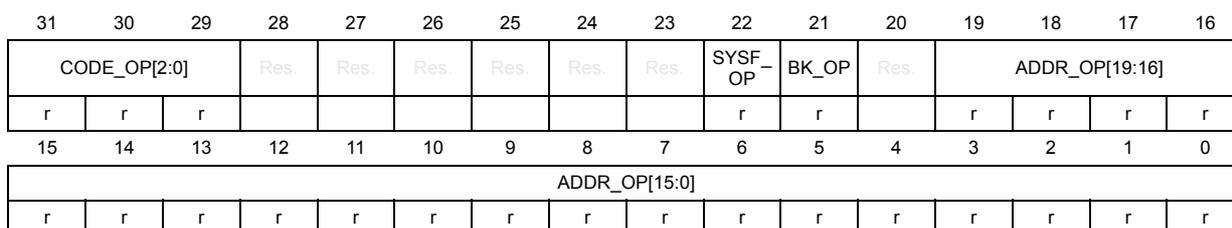
| 31 | 30 | 29 | 28 | 27 | 26 | 25 | 24 | 23 | 22 | 21 | 20 | 19 | 18 | 17 | 16 |
| CODE_OP[2:0] | Res. | Res. | Res. | Res. | Res. | Res. | SYSF_OP | BK_OP | Res. | ADDR_OP[19:16] | |||||
| r | r | r | r | r | r | r | r | r | |||||||
| 15 | 14 | 13 | 12 | 11 | 10 | 9 | 8 | 7 | 6 | 5 | 4 | 3 | 2 | 1 | 0 |
| ADDR_OP[15:0] | |||||||||||||||
| r | r | r | r | r | r | r | r | r | r | r | r | r | r | r | r |
Bits 31:29 CODE_OP[2:0] : Flash memory operation code
This bitfield indicates which flash memory operation has been interrupted by a system reset:
000: No flash operation interrupted by previous reset
001: Single write operation interrupted
010: Burst write operation interrupted
011: Page erase operation interrupted
100: Bank erase operation interrupted
101: Mass erase operation interrupted
110: Option change operation interrupted
111: Reserved
Bits 28:23 Reserved, must be kept at reset value.
Bit 22 SYSF_OP : Operation in system flash memory interrupted
This bit indicates that the reset occurred during an operation in the system flash memory.
Bit 21 BK_OP : Interrupted operation bank
This bit indicates which flash memory bank was accessed when reset occurred
0: Bank 1
1: Bank 2
Bit 20 Reserved, must be kept at reset value.
Bits 19:0 ADDR_OP[19:0] : Interrupted operation address
This bitfield indicates which address in the flash memory was accessed when reset occurred. The address is given by bank from address 0x0 0000.
Note: ADDR_OP[19] is reserved for STM32U375/385.
ADDR_OP[19:18] are reserved for STM32U356/366.
7.10.14 FLASH option register (FLASH_OPTR)
Address offset: 0x40
Reset value: 0xXXXX XXXX
This register is nonsecure. It can be read and written by both secure and nonsecure access. This register can be protected against unprivileged access when PRIV = 1 in FLASH_PRIVCFG register.
ST production value: 0x1FEF F0AA
(register bits 0 to 31 are loaded with values from the flash memory at OBL)
Access: no wait state when no option bytes modification is ongoing; word, half-word, and byte access.
Note: This alternate register description is not applicable to STM32U375/U385.
| 31 | 30 | 29 | 28 | 27 | 26 | 25 | 24 | 23 | 22 | 21 | 20 | 19 | 18 | 17 | 16 |
|---|---|---|---|---|---|---|---|---|---|---|---|---|---|---|---|
| TZEN | IO_VD DIO2_ HSLV | IO_VD D_HSL V | Res. | NBOO T0 | NSWB OOT0 | SRAM2 _RST | SRAM2 _PE | SRAM3 _PE | Res. | DUALB ANK | SWAP_ BANK | WWDG _SW | IWDG STDBY | IWDG _STOP | IWDG _SW |
| rw | rw | rw | rw | rw | rw | rw | rw | rw | rw | rw | rw | rw | rw | ||
| 15 | 14 | 13 | 12 | 11 | 10 | 9 | 8 | 7 | 6 | 5 | 4 | 3 | 2 | 1 | 0 |
| SRAM _RST | NRST _SHDW | NRST _STDBY | NRST _STOP | BDRST _POR | BOR_LEV[2:0] | RDP[7:0] | |||||||||
| rw | rw | rw | rw | rw | rw | rw | rw | rw | rw | rw | rw | rw | rw | rw | rw |
Bit 31 TZEN : Global TrustZone security enable
0: Global TrustZone security disabled
1: Global TrustZone security enabled
Bit 30 IO_VDDIO2_HSLV : High-speed I/O at low V DDIO2 voltage configuration bit
This bit can be set only with V DDIO2 below 2.5 V.
0: High-speed I/O at low V DDIO2 voltage feature is not allowed. V DDIO2 can exceed 2.5 V.
1: High-speed I/O at low V DDIO2 voltage feature is allowed (refer to GPIOx_HSLVR register). V DDIO2 must remain below 2.5 V.
Bit 29 IO_VDD_HSLV : High-speed I/O at low V DD voltage configuration bit
This bit can be set only with V DD below 2.5 V.
0: High-speed I/O at low V DD voltage feature is not allowed. V DD can exceed 2.5 V.
1: High-speed I/O at low V DD voltage feature is allowed (refer to GPIOx_HSLVR register). V DD must remain below 2.5 V.
Bit 28 Reserved, must be kept at reset value.
Bit 27 NBOOT0 : NBOOT0 option bit
0: NBOOT0 = 0
1: NBOOT0 = 1
Bit 26 NSWBOOT0 : Software BOOT0
0: BOOT0 taken from the option bit NBOOT0
1: BOOT0 taken from PH3/BOOT0 pin
Bit 25 SRAM2_RST : SRAM2 erase when system reset
0: SRAM2 erased when a system reset occurs and upon exiting standby
1: SRAM2 not erased when a system reset occurs and upon exiting standby
Bit 24 SRAM2_PE : SRAM2 parity check enable
- 0: SRAM2 parity check enabled
- 1: SRAM2 parity check disabled
Bit 23 SRAM3_PE : SRAM3 parity check enable
- 0: SRAM3 parity check enabled
- 1: SRAM3 parity check disabled
Note: SRAM3 is not available on STM32U356/366.
Bit 22 Reserved, must be kept at reset value.
Bit 21 DUALBANK : Dual-bank configuration
- 0: Single-bank flash with contiguous address in bank 1
- 1: Dual-bank flash with contiguous addresses
Note: Single-bank flash with contiguous address in bank 1 is only available for devices with flash size equal to:
- - 256-Kbyte flash memory devices for STM32U356/366.
- - 1-Mbyte flash memory devices for STM32U3B5/3C5.
Bit 20 SWAP_BANK : Swap banks
- 0: Bank 1 and bank 2 addresses not swapped
- 1: Bank 1 and bank 2 addresses swapped
Bit 19 WWDG_SW : Window watchdog selection
- 0: Hardware WWDG selected
- 1: Software WWDG selected
Bit 18 IWDG_STDBY : Independent watchdog counter freeze in Standby mode
- 0: IWDG counter frozen in Standby mode
- 1: IWDG counter running in Standby mode
Bit 17 IWDG_STOP : Independent watchdog counter freeze in Stop mode
- 0: IWDG counter frozen in Stop mode
- 1: IWDG counter running in Stop mode
Bit 16 IWDG_SW : Independent watchdog selection
- 0: Hardware IWDG selected
- 1: Software IWDG selected
Bit 15 SRAM_RST : All SRAMs (except SRAM2 and SRAM4) erase upon system reset
- 0: All SRAMs (except SRAM2 and SRAM4) erased when a system reset occurs and upon exiting standby
- 1: All SRAMs (except SRAM2 and SRAM4) not erased when a system reset occurs and upon exiting standby
Note: SRAM4 is not available in STM32U356/366.
Bit 14 NRST_SHDW : Reset generation in Shutdown mode
- 0: Reset generated when entering the Shutdown mode
- 1: No reset generated when entering the Shutdown mode
Bit 13 NRST_STDBY : Reset generation in Standby mode
- 0: Reset generated when entering the Standby mode
- 1: No reset generated when entering the Standby mode
Bit 12 NRST_STOP : Reset generation in Stop mode
- 0: Reset generated when entering the Stop mode
- 1: No reset generated when entering the Stop mode
Bit 11 BDRST_POR : Backup domain reset with power-on reset
0: The backup domain is not reset after a \( V_{DD} \) domain brownout reset (BOR).
This configuration must be used when \( V_{BAT} \) supply source is different from \( V_{DD} \) .
1: The backup domain is reset after a \( V_{DD} \) domain brownout reset (BOR). This configuration must be used when the \( V_{BAT} \) and \( V_{DD} \) are connected together. It is forbidden when \( V_{BAT} \) supply source is different from \( V_{DD} \) .
Bits 10:8 BOR_LEV[2:0] : BOR reset level
This bitfield contains the \( V_{DD} \) supply level threshold that activates/releases the reset.
000: BOR level 0 (reset level threshold around 1.7 V)
001: BOR level 1 (reset level threshold around 2.0 V)
010: BOR level 2 (reset level threshold around 2.2 V)
011: BOR level 3 (reset level threshold around 2.5 V)
100: BOR level 4 (reset level threshold around 2.8 V)
Bits 7:0 RDP[7:0] : Readout protection level
0xAA: Level 0 (readout protection not active)
0x55: Level 0.5 (readout protection not active, only nonsecure debug access is possible).
Only available when TrustZone is active (TZEN = 1)
0xCC: Level 2 (chip readout protection active)
Others: Level 1 (memories readout protection active)
Note: Refer to Section 7.6.2: Readout protection (RDP) for more details.
7.10.15 FLASH option register [alternate] (FLASH_OPTR)
Address offset: 0x40
Reset value: 0xXXXX XXXX
This register is nonsecure. It can be read and written by both secure and nonsecure access.
This register can be protected against unprivileged access when PRIV = 1 in FLASH_PRIVCFG register.
ST production value: 0x1FEF F0AA
(register bits 0 to 31 are loaded with values from the flash memory at OBL)
Access: no wait state when no option bytes modification is ongoing; word, half-word, and byte access.
Note: This alternate register description is applicable only to STM32U375/U385.
| 31 | 30 | 29 | 28 | 27 | 26 | 25 | 24 | 23 | 22 | 21 | 20 | 19 | 18 | 17 | 16 |
|---|---|---|---|---|---|---|---|---|---|---|---|---|---|---|---|
| TZEN | IO_VD DIO2_ HSLV | IO_VD D_HSL V | Res. | NBOO T0 | NSWB OOT0 | SRAM2 _RST | SRAM2 _PE | BL_IO_VDDIO2 _HSLV[1:0] | DUALB ANK | SWAP_ BANK | WWDG _SW | IWDG STDBY | IWDG _STOP | IWDG _SW | |
| rw | rw | rw | rw | rw | rw | rw | rw | rw | rw | rw | rw | rw | rw | rw |
| 15 | 14 | 13 | 12 | 11 | 10 | 9 | 8 | 7 | 6 | 5 | 4 | 3 | 2 | 1 | 0 |
|---|---|---|---|---|---|---|---|---|---|---|---|---|---|---|---|
| SRAM1 _RST | NRST SHDW | NRST STDBY | NRST _STOP | BDRST _POR | BOR_LEV[2:0] | RDP[7:0] | |||||||||
| rw | rw | rw | rw | rw | rw | rw | rw | rw | rw | rw | rw | rw | rw | rw | rw |
Bit 31 TZEN : Global TrustZone security enable
0: Global TrustZone security disabled
1: Global TrustZone security enabled
- Bit 30
IO_VDDIO2_HSLV
: High-speed I/O at low
\(
V_{DDIO2}
\)
voltage configuration bit
This bit can be set only with \( V_{DDIO2} \) below 2.5 V.
0: High-speed I/O at low \( V_{DDIO2} \) voltage feature is not allowed. \( V_{DDIO2} \) can exceed 2.5 V.
1: High-speed I/O at low \( V_{DDIO2} \) voltage feature is allowed (refer to GPIOx_HSLVR register). \( V_{DDIO2} \) must remain below 2.5 V. - Bit 29
IO_VDD_HSLV
: High-speed I/O at low
\(
V_{DD}
\)
voltage configuration bit
This bit can be set only with \( V_{DD} \) below 2.5 V.
0: High-speed I/O at low \( V_{DD} \) voltage feature is not allowed. \( V_{DD} \) can exceed 2.5 V.
1: High-speed I/O at low \( V_{DD} \) voltage feature is allowed (refer to GPIOx_HSLVR register). \( V_{DD} \) must remain below 2.5 V. - Bit 28 Reserved, must be kept at reset value.
- Bit 27
NBOOT0
: NBOOT0 option bit
0: NBOOT0 = 0
1: NBOOT0 = 1 - Bit 26
NSWBOOT0
: Software BOOT0
0: BOOT0 taken from the option bit NBOOT0
1: BOOT0 taken from PH3/BOOT0 pin - Bit 25
SRAM2_RST
: SRAM2 erase when system reset
0: SRAM2 erased when a system reset occurs
1: SRAM2 not erased when a system reset occurs - Bit 24
SRAM2_PE
: SRAM2 parity check enable
0: SRAM2 parity check enabled
1: SRAM2 parity check disabled - Bits 23:22
BL_IO_VDDIO2_HSLV[1:0]
: Bootloader usage of high-speed I/O at low
\(
V_{DDIO2}
\)
voltage on PG2, PG3, PG4, and PG5.
These bits are considered only if IO_VDDIO2_HSLV is set.
00: Bootloader is allowed to enable HSLV on PG2, PG3, PG4 and PG5.
11: Bootloader is not allowed to enable HSLV on PG2, PG3, PG4 and PG5.
Others: Reserved. - Bit 21
DUALBANK
: Dual-bank configuration
0: Single-bank FLASH with contiguous address in bank 1
1: Dual-bank FLASH with contiguous addresses
Note: Single-bank flash with contiguous address in bank 1 is only available for devices with flash size equal to:
- 512-Kbyte flash memory devices for STM32U375/385 - Bit 20
SWAP_BANK
: Swap banks
0: Bank 1 and bank 2 addresses not swapped
1: Bank 1 and bank 2 addresses swapped - Bit 19
WWDG_SW
: Window watchdog selection
0: Hardware WWDG selected
1: Software WWDG selected - Bit 18
IWDG_STDBY
: Independent watchdog counter freeze in Standby mode
0: IWDG counter frozen in Standby mode
1: IWDG counter running in Standby mode
Bit 17 IWDG_STOP : Independent watchdog counter freeze in Stop mode
- 0: IWDG counter frozen in Stop mode
- 1: IWDG counter running in Stop mode
Bit 16 IWDG_SW : Independent watchdog selection
- 0: Hardware IWDG selected
- 1: Software IWDG selected
Bit 15 SRAM1_RST : SRAM1 erase upon system reset
- 0: SRAM1 erased when a system reset occurs
- 1: SRAM1 not erased when a system reset occurs
Bit 14 NRST_SHDW : Reset generation in Shutdown mode
- 0: Reset generated when entering the Shutdown mode
- 1: No reset generated when entering the Shutdown mode
Bit 13 NRST_STDBY : Reset generation in Standby mode
- 0: Reset generated when entering the Standby mode
- 1: No reset generated when entering the Standby mode
Bit 12 NRST_STOP : Reset generation in Stop mode
- 0: Reset generated when entering the Stop mode
- 1: No reset generated when entering the Stop mode
Bit 11 BDRST_POR : Backup domain reset with power-on reset
- 0: The backup domain is not reset after a \( V_{DD} \) domain brownout reset (BOR). This configuration must be used when \( V_{BAT} \) supply source is different from \( V_{DD} \) .
- 1: The backup domain is reset after a \( V_{DD} \) domain brownout reset (BOR). This configuration must be used when the \( V_{BAT} \) and \( V_{DD} \) are connected together. It is forbidden when \( V_{BAT} \) supply source is different from \( V_{DD} \) .
Bits 10:8 BOR_LEV[2:0] : BOR reset level
- This bitfield contains the \( V_{DD} \) supply level threshold that activates/releases the reset.
- 000: BOR level 0 (reset level threshold around 1.7 V)
- 001: BOR level 1 (reset level threshold around 2.0 V)
- 010: BOR level 2 (reset level threshold around 2.2 V)
- 011: BOR level 3 (reset level threshold around 2.5 V)
- 100: BOR level 4 (reset level threshold around 2.8 V)
Bits 7:0 RDP[7:0] : Readout protection level
- 0xAA: Level 0 (readout protection not active)
- 0x55: Level 0.5 (readout protection not active, only nonsecure debug access is possible).
Only available when TrustZone is active (TZEN = 1) - 0xCC: Level 2 (chip readout protection active)
- Others: Level 1 (memories readout protection active)
Note: Refer to Section 7.6.2: Readout protection (RDP) for more details.
7.10.16 FLASH nonsecure boot address 0 register (FLASH_BOOT0R)
Address offset: 0x44
Reset value: 0xXXXX XXXF
This register can not be written if OPTLOCK bit is set.
This register is nonsecure. It can be read and written by both secure and nonsecure access. This register can be protected against unprivileged access when PRIV = 1 in FLASH_PRIVCFG register.
ST production value: 0x0800 007F
(option bytes are loaded with values from the flash memory at reset release)
Access: no wait state when no option bytes modification is ongoing; word, half-word, and byte access.
| 31 | 30 | 29 | 28 | 27 | 26 | 25 | 24 | 23 | 22 | 21 | 20 | 19 | 18 | 17 | 16 |
|---|---|---|---|---|---|---|---|---|---|---|---|---|---|---|---|
| ADD[24:9] | |||||||||||||||
| rw | rw | rw | rw | rw | rw | rw | rw | rw | rw | rw | rw | rw | rw | rw | rw |
| 15 | 14 | 13 | 12 | 11 | 10 | 9 | 8 | 7 | 6 | 5 | 4 | 3 | 2 | 1 | 0 |
| ADD[8:0] | Res. | Res. | Res. | Res. | Res. | Res. | |||||||||
| rw | rw | rw | rw | rw | rw | rw | rw | rw | |||||||
Bits 31:7 ADD[24:0] : Nonsecure boot base address 0
The nonsecure boot memory address can be programmed to any address in the valid address range with a granularity of 128 bytes. These bits correspond to address [31:7].
ADD option bytes are selected following the BOOT0 pin or NSWBOOT0 state.
Examples:
ADD[24:0] = 0x0100000: Boot from nonsecure flash memory (0x0800 0000)
ADD[24:0] = 0x017F1E0: Boot from system memory bootloader (0x0BF8 F000)
ADD[24:0] = 0x0400000: Boot from nonsecure SRAM1 on S-Bus (0x2000 0000)
Bits 6:0 Reserved, must be kept at reset value.
7.10.17 FLASH nonsecure boot address 1 register (FLASH_BOOT1R)
Address offset: 0x48
Reset value: 0xXXXX XXXF
This register can not be written if OPTLOCK bit is set.
This register is nonsecure. It can be read and written by both secure and nonsecure access. This register can be protected against unprivileged access when PRIV = 1 in FLASH_PRIVCFG register.
ST production value: 0x0BF8 F07F
(option bytes are loaded with values from the flash memory at reset release)
Access: no wait state when no option bytes modification is ongoing; word, half-word, and byte access.
| 31 | 30 | 29 | 28 | 27 | 26 | 25 | 24 | 23 | 22 | 21 | 20 | 19 | 18 | 17 | 16 |
|---|---|---|---|---|---|---|---|---|---|---|---|---|---|---|---|
| ADD[24:9] | |||||||||||||||
| rw | rw | rw | rw | rw | rw | rw | rw | rw | rw | rw | rw | rw | rw | rw | rw |
| 15 | 14 | 13 | 12 | 11 | 10 | 9 | 8 | 7 | 6 | 5 | 4 | 3 | 2 | 1 | 0 |
| ADD[8:0] | Res. | Res. | Res. | Res. | Res. | Res. | Res. | ||||||||
| rw | rw | rw | rw | rw | rw | rw | rw | rw | |||||||
Bits 31:7 ADD[24:0] : nonsecure boot address 1
The nonsecure boot memory address can be programmed to any address in the valid address range with a granularity of 128 bytes. These bits correspond to address [31:7].
ADD option bytes are selected following the BOOT0 pin or nSWBOOT0 state.
Examples:
ADD[24:0] = 0x0100000: Boot from nonsecure flash memory (0x0800 0000)
ADD[24:0] = 0x017F1E0: Boot from system memory bootloader (0x0BF8 F000)
ADD[24:0] = 0x0400000: Boot from nonsecure SRAM1 on S-Bus (0x2000 0000)
Bits 6:0 Reserved, must be kept at reset value.
7.10.18 FLASH secure boot address 0 register (FLASH_SBOOT0R)
Address offset: 0x4C
Reset value: 0xXXXX XXXX
This register can not be written if OPTLOCK bit is set.
This register is secure. It can be read and written only by secure access. A nonsecure read/write access is RAZ/WI. This register can be protected against unprivileged access when SPRIV = 1 in FLASH_PRIVCFG register.
ST production value: 0x0C00 007C
(option bytes are loaded with values from the flash memory at reset release)
Access: no wait state when no option bytes modification is ongoing; word, half-word, and byte access.
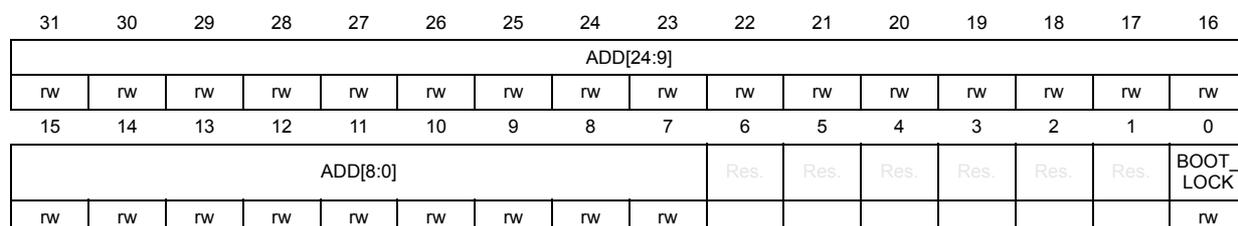
| 31 | 30 | 29 | 28 | 27 | 26 | 25 | 24 | 23 | 22 | 21 | 20 | 19 | 18 | 17 | 16 |
| ADD[24:9] | |||||||||||||||
| rw | rw | rw | rw | rw | rw | rw | rw | rw | rw | rw | rw | rw | rw | rw | rw |
| 15 | 14 | 13 | 12 | 11 | 10 | 9 | 8 | 7 | 6 | 5 | 4 | 3 | 2 | 1 | 0 |
| ADD[8:0] | Res. | Res. | Res. | Res. | Res. | Res. | BOOT_LOCK | ||||||||
| rw | rw | rw | rw | rw | rw | rw | rw | rw | rw | ||||||
Bits 31:7 ADD[24:0] : Secure boot base address 0
The secure boot memory address can be programmed to any address in the valid address range with a granularity of 128 bytes. This bits correspond to address [31:7] ADD option bytes are selected following the BOOT0 pin or NSWBOOT0 state.
Examples:
ADD[24:0] = 0x018 0000: Boot from secure flash memory (0x0C00 0000)
ADD[24:0] = 0x01F F000: Boot from RSS (0x0FF8 0000)
ADD[24:0] = 0x060 0000: Boot from secure SRAM1 on S-Bus (0x3000 0000)
Bits 6:1 Reserved, must be kept at reset value.
Bit 0 BOOT_LOCK : Boot lock
When set, the boot is always forced to base address value programmed in ADD[24:0] option bytes, whatever the boot selection option. When set, this bit can only be cleared when RDP is at level 0.
7.10.19 FLASH secure watermark1 register 1 (FLASH_SECWM1R1)
Address offset: 0x50
Reset value: 0xFFXX FFXX
This register can not be written if OPTLOCK bit is set.
This register is secure. It can be read and written only by secure access. A nonsecure read/write access is RAZ/WI. This register can be protected against unprivileged access when SPRIV = 1 in FLASH_PRIVCFGR register.
ST production value:
- • 0xFFFF FFC0 (for STM32U356/366)
- • 0xFFFF FF80 (for STM32U375/385)
- • 0xFFFF FF00 (for STM32U3B5/3C5)
(register bits are loaded with values from the flash memory at OBL. Reserved bits are read as 1.)
Access: no wait state when no option bytes modification is ongoing; word, half-word, and byte access.
| 31 | 30 | 29 | 28 | 27 | 26 | 25 | 24 | 23 | 22 | 21 | 20 | 19 | 18 | 17 | 16 |
|---|---|---|---|---|---|---|---|---|---|---|---|---|---|---|---|
| Res. | Res. | Res. | Res. | Res. | Res. | Res. | Res. | SECWM1_END[7:0] | |||||||
| rw | rw | rw | rw | rw | rw | rw | rw | ||||||||
| 15 | 14 | 13 | 12 | 11 | 10 | 9 | 8 | 7 | 6 | 5 | 4 | 3 | 2 | 1 | 0 |
|---|---|---|---|---|---|---|---|---|---|---|---|---|---|---|---|
| Res. | Res. | Res. | Res. | Res. | Res. | Res. | Res. | SECWM1_STRT[7:0] | |||||||
| rw | rw | rw | rw | rw | rw | rw | rw | ||||||||
Bits 31:24 Reserved, must be kept at reset value.
Bits 23:16 SECWM1_END[7:0] : End page of first secure area
This bitfield contains the last page of the secure area in bank 1.
Note: SECWM1_END[7:6] are reserved for STM32U356/366.
SECWM1_END[7] is reserved for STM32U375/385.
Bits 15:8 Reserved, must be kept at reset value.
Bits 7:0 SECWM1_STRT[7:0] : Start page of first secure area
This bitfield contains the first page of the secure area in bank 1.
Note: SECWM1_STRT[7:6] are reserved for STM32U356/366.
SECWM1_STRT[7] is reserved for STM32U375/385.
7.10.20 FLASH secure watermark1 register 2 (FLASH_SECWM1R2)
Address offset: 0x54
Reset value: 0xXXXX FFFF
This register can not be written if OPTLOCK bit is set.
This register is secure. It can be read and written only by secure access. A nonsecure read/write access is RAZ/WI. This register can be protected against unprivileged access when SPRIV = 1 in FLASH_PRIVCFGR register.
ST production value:
- • 0xB4C0 FFFF (for STM32U356/366)
- • 0xB480 FFFF (for STM32U375/385)
- • 0xB400 FFFF (for STM32U3B5/3C5)
(register bits are loaded with values from the flash memory at OBL)
Access: no wait state when no option bytes modification is ongoing; word, half-word, and byte access
| 31 | 30 | 29 | 28 | 27 | 26 | 25 | 24 | 23 | 22 | 21 | 20 | 19 | 18 | 17 | 16 |
|---|---|---|---|---|---|---|---|---|---|---|---|---|---|---|---|
| HDP1EN[7:0] | HDP1_END[7:0] | ||||||||||||||
| rw | rw | rw | rw | rw | rw | rw | rw | rw | rw | rw | rw | rw | rw | rw | rw |
| 15 | 14 | 13 | 12 | 11 | 10 | 9 | 8 | 7 | 6 | 5 | 4 | 3 | 2 | 1 | 0 |
| Res. | Res. | Res. | Res. | Res. | Res. | Res. | Res. | Res. | Res. | Res. | Res. | Res. | Res. | Res. | Res. |
Bits 31:24 HDP1EN[7:0] : Hide protection first area enable
0xB4: No HDP area 1
others: HDP first area enabled
Bits 23:16 HDP1_END[7:0] : End page of first hide protection area
This bitfield contains the last page of the HDP area in bank 1.
Note: HDP1_END[7:6] are reserved for STM32U356/366.
HDP1_END[7] is reserved for STM32U375/385
Bits 15:0 Reserved, must be kept at reset value.
7.10.21 FLASH WRP1 area A address register (FLASH_WRP1AR)
Address offset: 0x58
Reset value: 0xFFXX FFXX
This register can not be written if OPTLOCK bit is set.
This register is nonsecure. It can be read and written by both secure and nonsecure access. This register can be protected against unprivileged access when PRIV = 1 in FLASH_PRIVCFGR register.
ST production value:
- • 0xFFC0 FFFF (for STM32U356/366)
- • 0xFF80 FFFF (for STM32U375/385)
- • 0xFF00 FFFF (for STM32U3B5/3C5)
(register bits are loaded with values from the flash memory at OBL. Reserved bits are read as 1)
Access: no wait state when no option bytes modification is ongoing; word, half-word, and byte access
| 31 | 30 | 29 | 28 | 27 | 26 | 25 | 24 | 23 | 22 | 21 | 20 | 19 | 18 | 17 | 16 |
|---|---|---|---|---|---|---|---|---|---|---|---|---|---|---|---|
| UNLOCK | Res. | Res. | Res. | Res. | Res. | Res. | Res. | END[7:0] | |||||||
| rw | rw | rw | rw | rw | rw | rw | rw | rw | |||||||
| 15 | 14 | 13 | 12 | 11 | 10 | 9 | 8 | 7 | 6 | 5 | 4 | 3 | 2 | 1 | 0 |
| Res. | Res. | Res. | Res. | Res. | Res. | Res. | Res. | STRT[7:0] | |||||||
| rw | rw | rw | rw | rw | rw | rw | rw | ||||||||
Bit 31 UNLOCK : Bank 1 WPR first area A unlock
0: WRP1A start and end pages locked
1: WRP1A start and end pages unlocked
Bits 30:24 Reserved, must be kept at reset value.
Bits 23:16 END[7:0] : Bank 1 WPR first area A end page
This bitfield contains the last page of the first WPR area in bank 1.
Note: END[7:6] are reserved for STM32U356/366.
END[7] is reserved for STM32U375/385.
Bits 15:8 Reserved, must be kept at reset value.
Bits 7:0 STRT[7:0] : Bank 1 WPR first area A start page
This bitfield contains the first page of the first WPR area for bank 1.
Note: STRT[7:6] are reserved for STM32U356/366.
STRT[7] is reserved for STM32U375/385.
7.10.22 FLASH WRP1 area B address register (FLASH_WRP1BR)
Address offset: 0x5C
Reset value: 0xFFXX FFXX
This register can not be written if OPTLOCK bit is set.
This register is nonsecure. It can be read and written by both secure and nonsecure access.
This register can be protected against unprivileged access when PRIV = 1 in FLASH_PRIVCFG register.
ST production value:
- • 0xFFC0 FFFF (for STM32U356/366)
- • 0xFF80 FFFF (for STM32U375/385)
- • 0xFF00 FFFF (for STM32U3B5/3C5)
(register bits are loaded with values from the flash memory at OBL)
Access: no wait state when no option bytes modification is ongoing; word, half-word, and byte access
| 31 | 30 | 29 | 28 | 27 | 26 | 25 | 24 | 23 | 22 | 21 | 20 | 19 | 18 | 17 | 16 |
|---|---|---|---|---|---|---|---|---|---|---|---|---|---|---|---|
| UNLOCK | Res. | Res. | Res. | Res. | Res. | Res. | Res. | END[7:0] | |||||||
| rw | rw | rw | rw | rw | rw | rw | rw | rw | |||||||
| 15 | 14 | 13 | 12 | 11 | 10 | 9 | 8 | 7 | 6 | 5 | 4 | 3 | 2 | 1 | 0 |
| Res. | Res. | Res. | Res. | Res. | Res. | Res. | Res. | STRT[7:0] | |||||||
| rw | rw | rw | rw | rw | rw | rw | rw | ||||||||
Bit 31 UNLOCK : Bank 1 WPR second area B unlock
0: WRP1B start and end pages locked
1: WRP1B start and end pages unlocked
Bits 30:24 Reserved, must be kept at reset value.
Bits 23:16 END[7:0] : Bank 1 WRP second area B end page
This bitfield contains the last page of the second WRP area in bank 1.
Note: END[7:6] are reserved for STM32U356/366.
END[7] is reserved for STM32U375/385.
Bits 15:8 Reserved, must be kept at reset value.
Bits 7:0 STRT[7:0] : Bank 1 WRP second area B start page
This bitfield contains the first page of the second WRP area for bank 1.
Note: STRT[7:6] are reserved for STM32U356/366.
STRT[7] is reserved for STM32U375/385.
7.10.23 FLASH secure watermark2 register 1 (FLASH_SECWM2R1)
Address offset: 0x60
Reset value: 0xFFXX FFXX
This register can not be written if OPTLOCK bit is set.
This register is secure. It can be read and written only by secure access. A nonsecure read/write access is RAZ/WI. This register can be protected against unprivileged access when SPRIV = 1 in FLASH_PRIVCFGR register.
ST production value:
- • 0xFFFF FFC0 (for STM32U356/366)
- • 0xFFFF FF80 (for STM32U375/385)
- • 0xFFFF FF00 (for STM32U3B5/3C5)
(register bits are loaded with values from the flash memory at OBL)
Access: no wait state when no option bytes modification is ongoing; word, half-word, and byte access
| 31 | 30 | 29 | 28 | 27 | 26 | 25 | 24 | 23 | 22 | 21 | 20 | 19 | 18 | 17 | 16 |
|---|---|---|---|---|---|---|---|---|---|---|---|---|---|---|---|
| Res. | Res. | Res. | Res. | Res. | Res. | Res. | Res. | SECWM2_END[7:0] | |||||||
| rw | rw | rw | rw | rw | rw | rw | rw | ||||||||
| 15 | 14 | 13 | 12 | 11 | 10 | 9 | 8 | 7 | 6 | 5 | 4 | 3 | 2 | 1 | 0 |
| Res. | Res. | Res. | Res. | Res. | Res. | Res. | Res. | SECWM2_STRT[7:0] | |||||||
| rw | rw | rw | rw | rw | rw | rw | rw | ||||||||
Bits 31:24 Reserved, must be kept at reset value.
Bits 23:16 SECWM2_END[7:0] : End page of second secure area
This bitfield contains the last page of the secure area in bank 2.
Note: SECWM2_END[7:6] are reserved for STM32U356/366.
SECWM2_END[7] is reserved for STM32U375/385.
Bits 15:8 Reserved, must be kept at reset value.
Bits 7:0 SECWM2_STRT[7:0] : Start page of second secure area
This bitfield contains the first page of the secure area in bank 2.
Note: SECWM2_STRT[7:6] are reserved for STM32U356/366.
SECWM2_STRT[7] is reserved for STM32U375/385.
7.10.24 FLASH secure watermark2 register 2 (FLASH_SECWM2R2)
Address offset: 0x64
Reset value: 0xXXXX FFFF
This register can not be written if OPTLOCK bit is set.
This register is secure. It can be read and written only by secure access. A nonsecure read/write access is RAZ/WI. This register can be protected against unprivileged access when SPRIV = 1 in FLASH_PRIVCFGR register.
ST production value:
- • 0xB4C0 FFFF (for STM32U356/366)
- • 0xB480 FFFF (for STM32U375/385)
- • 0xB400 FFFF (for STM32U3B5/3C5)
(register bits are loaded with values from the flash memory at OBL)
Access: no wait state when no option bytes modification is ongoing; word, half-word, and byte access
| 31 | 30 | 29 | 28 | 27 | 26 | 25 | 24 | 23 | 22 | 21 | 20 | 19 | 18 | 17 | 16 |
|---|---|---|---|---|---|---|---|---|---|---|---|---|---|---|---|
| HDP2EN[7:0] | HDP2_END[7:0] | ||||||||||||||
| rw | rw | rw | rw | rw | rw | rw | rw | rw | rw | rw | rw | rw | rw | rw | rw |
| 15 | 14 | 13 | 12 | 11 | 10 | 9 | 8 | 7 | 6 | 5 | 4 | 3 | 2 | 1 | 0 |
| Res. | Res. | Res. | Res. | Res. | Res. | Res. | Res. | Res. | Res. | Res. | Res. | Res. | Res. | Res. | Res. |
Bits 31:24 HDP2EN[7:0] : Hide protection second area enable
0xB4: No HDP area 2
others: HDP second area is enabled.
Bits 23:16 HDP2_END[7:0] : End page of hide protection second area
This bitfield contains the last page of the HDP area in bank 2.
Note: HDP2_END[7:6] are reserved for STM32U356/366.
HDP2_END[7] is reserved for STM32U375/385.
Bits 15:0 Reserved, must be kept at reset value.
7.10.25 FLASH WPR2 area A address register (FLASH_WRP2AR)
Address offset: 0x68
Reset value: 0xFFXX FFXX
This register can not be written if OPTLOCK bit is set.
This register is nonsecure. It can be read and written by both secure and nonsecure access.
This register can be protected against unprivileged access when PRIV = 1 in FLASH_PRIVCFG register.
ST production value:
- • 0xFFC0 FFFF (for STM32U356/366)
- • 0xFF80 FFFF (for STM32U375/385)
- • 0xFF00 FFFF (for STM32U3B5/3C5)
(register bits are loaded with values from the flash memory at OBL)
Access: no wait state when no option bytes modification is ongoing; word, half-word, and byte access
| 31 | 30 | 29 | 28 | 27 | 26 | 25 | 24 | 23 | 22 | 21 | 20 | 19 | 18 | 17 | 16 |
|---|---|---|---|---|---|---|---|---|---|---|---|---|---|---|---|
| UNLOCK | Res. | Res. | Res. | Res. | Res. | Res. | Res. | END[7:0] | |||||||
| rw | rw | rw | rw | rw | rw | rw | rw | rw | |||||||
| 15 | 14 | 13 | 12 | 11 | 10 | 9 | 8 | 7 | 6 | 5 | 4 | 3 | 2 | 1 | 0 |
| Res. | Res. | Res. | Res. | Res. | Res. | Res. | Res. | STRT[7:0] | |||||||
| rw | rw | rw | rw | rw | rw | rw | rw | ||||||||
Bit 31 UNLOCK : Bank 2 WPR first area A unlock
0: WRP2A start and end pages locked
1: WRP2A start and end pages unlocked
Bits 30:24 Reserved, must be kept at reset value.
Bits 23:16 END[7:0] : Bank 2 WPR first area A end page
This bitfield contains the last page of the first WRP area in bank 2.
Note: END[7:6] are reserved for STM32U356/366.
END[7] is reserved for STM32U375/385.
Bits 15:8 Reserved, must be kept at reset value.
Bits 7:0 STRT[7:0] : Bank 2 WPR first area A start page
This bitfield contains the first page of the first WRP area for bank 2.
Note: STRT[7:6] are reserved for STM32U356/366.
STRT[7] is reserved for STM32U375/385.
7.10.26 FLASH WPR2 area B address register (FLASH_WRP2BR)
Address offset: 0x6C
Reset value: 0xFFXX FFXX
This register can not be written if OPTLOCK bit is set.
This register is nonsecure. It can be read and written by both secure and nonsecure access.
This register can be protected against unprivileged access when PRIV = 1 in FLASH_PRIVCFGR register.
ST production value:
- • 0xFFC0 FFFF (for STM32U356/366)
- • 0xFF80 FFFF (for STM32U375/385)
- • 0xFF00 FFFF (for STM32U3B5/3C5)
(register bits are loaded with values from the flash memory at OBL)
Access: no wait state when no option bytes modification is ongoing; word, half-word, and byte access
| 31 | 30 | 29 | 28 | 27 | 26 | 25 | 24 | 23 | 22 | 21 | 20 | 19 | 18 | 17 | 16 |
|---|---|---|---|---|---|---|---|---|---|---|---|---|---|---|---|
| UNLOCK | Res. | Res. | Res. | Res. | Res. | Res. | Res. | END[7:0] | |||||||
| rw | rw | rw | rw | rw | rw | rw | rw | rw | |||||||
| 15 | 14 | 13 | 12 | 11 | 10 | 9 | 8 | 7 | 6 | 5 | 4 | 3 | 2 | 1 | 0 |
| Res. | Res. | Res. | Res. | Res. | Res. | Res. | Res. | STRT[7:0] | |||||||
| rw | rw | rw | rw | rw | rw | rw | rw | ||||||||
Bit 31 UNLOCK : Bank 2 WPR second area B unlock
0: WRP2B start and end pages locked
1: WRP2B start and end pages unlocked
Bits 30:24 Reserved, must be kept at reset value.
Bits 23:16 END[7:0] : Bank 2 WPR second area B end page
This bitfield contains the last page of the second WRP area in bank 2.
Note: END[7:6] are reserved for STM32U356/366.
END[7] is reserved for STM32U375/385.
Bits 15:8 Reserved, must be kept at reset value.
Bits 7:0 STRT[7:0] : Bank 2 WPR second area B start page
This bitfield contains the first page of the second WRP area for bank 2.
Note: STRT[7:6] are reserved for STM32U356/366.
STRT[7] is reserved for STM32U375/385.
7.10.27 FLASH secure block based bank 1 register x (FLASH_SECB1Rx)
Address offset: \( 0x80 + 0x4 \cdot (x - 1) \) , ( \( x = 1 \) to \( 8 \) )
Reset value: 0x0000 0000
This register is secure. It can be written only by secure access. This register can be protected against unprivileged access (refer to Table 69: FLASH_SECBByRx registers access when TrustZone is active (TZEN = 1) ).
FLASH secure block based bank 1 register x ( \( x = 3 \) to \( 4 \) ) are only available in STM32U375/385 and STM32U3B5/3C5.
FLASH secure block based bank 1 register x ( \( x = 5 \) to \( 8 \) ) are only available in STM32U3B5/3C5.
Access: no wait state; word, half-word, and byte access
| 31 | 30 | 29 | 28 | 27 | 26 | 25 | 24 | 23 | 22 | 21 | 20 | 19 | 18 | 17 | 16 |
|---|---|---|---|---|---|---|---|---|---|---|---|---|---|---|---|
| SEC31 | SEC30 | SEC29 | SEC28 | SEC27 | SEC26 | SEC25 | SEC24 | SEC23 | SEC22 | SEC21 | SEC20 | SEC19 | SEC18 | SEC17 | SEC16 |
| rw | rw | rw | rw | rw | rw | rw | rw | rw | rw | rw | rw | rw | rw | rw | rw |
| 15 | 14 | 13 | 12 | 11 | 10 | 9 | 8 | 7 | 6 | 5 | 4 | 3 | 2 | 1 | 0 |
| SEC15 | SEC14 | SEC13 | SEC12 | SEC11 | SEC10 | SEC9 | SEC8 | SEC7 | SEC6 | SEC5 | SEC4 | SEC3 | SEC2 | SEC1 | SEC0 |
| rw | rw | rw | rw | rw | rw | rw | rw | rw | rw | rw | rw | rw | rw | rw | rw |
Bits 31:0 SECi : Page secure/nonsecure attribution ( \( i = 31 \) to \( 0 \) )
Each bit is used to set one page security attribution in bank 1.
0: Page \( (32 \cdot \{x\} - 1) + \{i\} \) in bank 1 not block-based secure
1: Page \( (32 \cdot \{x\} - 1) + \{i\} \) in bank 1 block-based secure
7.10.28 FLASH secure block based bank 2 register x (FLASH_SECB2Rx)
Address offset: \( 0xA0 + 0x4 \cdot (x - 1) \) , ( \( x = 1 \) to \( 8 \) )
Reset value: 0x0000 0000
This register is secure. It can be written only by a secure access. This register can be protected against unprivileged access (refer to Table 69: FLASH_SECBByRx registers access when TrustZone is active (TZEN = 1) ).
FLASH secure block based bank 2 register x ( \( x = 5 \) to \( 8 \) ) are only available in STM32U3B5/3C5.
FLASH secure block based bank 2 register x ( \( x = 3 \) to \( 4 \) ) are only available in STM32U375/385 and STM32U3B5/3C5.
Access: no wait state; word, half-word, and byte access
| 31 | 30 | 29 | 28 | 27 | 26 | 25 | 24 | 23 | 22 | 21 | 20 | 19 | 18 | 17 | 16 |
|---|---|---|---|---|---|---|---|---|---|---|---|---|---|---|---|
| SEC31 | SEC30 | SEC29 | SEC28 | SEC27 | SEC26 | SEC25 | SEC24 | SEC23 | SEC22 | SEC21 | SEC20 | SEC19 | SEC18 | SEC17 | SEC16 |
| rw | rw | rw | rw | rw | rw | rw | rw | rw | rw | rw | rw | rw | rw | rw | rw |
| 15 | 14 | 13 | 12 | 11 | 10 | 9 | 8 | 7 | 6 | 5 | 4 | 3 | 2 | 1 | 0 |
| SEC15 | SEC14 | SEC13 | SEC12 | SEC11 | SEC10 | SEC9 | SEC8 | SEC7 | SEC6 | SEC5 | SEC4 | SEC3 | SEC2 | SEC1 | SEC0 |
| rw | rw | rw | rw | rw | rw | rw | rw | rw | rw | rw | rw | rw | rw | rw | rw |
Bits 31:0 SECi : Page secure/nonsecure attribution (i = 31 to 0)
Each bit is used to set one page security attribution in bank 2.
0: Page \( (32 * \{x\} - 1) + \{i\} \) in bank 2 not block-based secure
1: Page \( (32 * \{x\} - 1) + \{i\} \) in bank 2 block-based secure
7.10.29 FLASH secure HDP control register (FLASH_SECHDPCR)
Address offset: 0xC0
Reset value: 0xA3A3 A3A3
This register is secure. It can be read and written only by secure access. A nonsecure read/write access is RAZ/WI. This register can be protected against unprivileged access when SPRIV = 1 in FLASH_PRIVCFGR register.
Access: no wait state; word, half-word, and byte access
| 31 | 30 | 29 | 28 | 27 | 26 | 25 | 24 | 23 | 22 | 21 | 20 | 19 | 18 | 17 | 16 |
|---|---|---|---|---|---|---|---|---|---|---|---|---|---|---|---|
| HDP2EXT_ACCDIS[7:0] | HDP1EXT_ACCDIS[7:0] | ||||||||||||||
| rw | rw | rw | rw | rw | rw | rw | rw | rw | rw | rw | rw | rw | rw | rw | rw |
| 15 | 14 | 13 | 12 | 11 | 10 | 9 | 8 | 7 | 6 | 5 | 4 | 3 | 2 | 1 | 0 |
| HDP2_ACCDIS[7:0] | HDP1_ACCDIS[7:0] | ||||||||||||||
| rw | rw | rw | rw | rw | rw | rw | rw | rw | rw | rw | rw | rw | rw | rw | rw |
Bits 31:24 HDP2EXT_ACCDIS[7:0] : HDP2 extension area access disable
Register access depends on its current value. Refer to HDP extension area access for the full conditions.
- 0xA3: Access to HDP2 extension area granted
- 0x5C: Access to HDP2 extension area and HDP2 area denied, but HDP2_EXT (in FLASH_HDPEXTR) increment allowed at any time. (SECWM2Ry option bytes modification blocked - refer to Rules for modifying specific option bytes ).
- Others: Access to HDP2 extension area and HDP2 area denied. Update of HDP2_EXT size is not possible anymore. (SECWM2Ry option bytes modification blocked - refer to Rules for modifying specific option bytes )
Bits 23:16 HDP1EXT_ACCDIS[7:0] : HDP1 extension area access disable
Register access depends on its current value. Refer to HDP extension area access for the full conditions.
- 0xA3: Access to HDP1 extension area granted
- 0x5C: Access to HDP1 extension area and HDP1 area denied, but HDP1_EXT (in FLASH_HDPEXTR) increment allowed at any time. (SECWM1Ry option bytes modification blocked - refer to Rules for modifying specific option bytes )
- Others: Access to HDP1 extension area and HDP1 area denied. Update of HDP1_EXT size is not possible anymore. (SECWM1Ry option bytes modification blocked - refer to Rules for modifying specific option bytes )
Bits 15:8 HDP2_ACCDIS[7:0] : HDP2 area access disable
When set to a value different than 0xA3, this bitfield cannot be modified except by a system reset.
- 0xA3: Access to HDP2 area granted
- Others: Access to HDP2 area denied (SECWM2Ry option-byte modification blocked - refer to Rules for modifying specific option bytes ). When HDP2_ACCDIS value is different than 0xA3, any write access to HDP2_ACCDIS is ignored.
Bits 7:0 HDP1_ACCDIS[7:0] : HDP1 area access disable
When set to a value different than 0xA3, this bitfield cannot be modified except by a system reset.
0xA3: Access to HDP1 area granted
Others: Access to HDP1 area denied (SECWM1Ry option bytes modification blocked - refer to Rules for modifying specific option bytes ). When HDP1_ACCDIS value is different than 0xA3, any write access to HDP1_ACCDIS is ignored.
7.10.30 FLASH privilege configuration register (FLASH_PRIVCFGR)
Address offset: 0xC4
Reset value: 0x0000 0000
This register can be read by both privileged and unprivileged access. PRIV is a nonsecure bit. SPRIV is a secure bit.
Access: no wait state; word, half-word, and byte access
| 31 | 30 | 29 | 28 | 27 | 26 | 25 | 24 | 23 | 22 | 21 | 20 | 19 | 18 | 17 | 16 |
|---|---|---|---|---|---|---|---|---|---|---|---|---|---|---|---|
| Res. | Res. | Res. | Res. | Res. | Res. | Res. | Res. | Res. | Res. | Res. | Res. | Res. | Res. | Res. | Res. |
| 15 | 14 | 13 | 12 | 11 | 10 | 9 | 8 | 7 | 6 | 5 | 4 | 3 | 2 | 1 | 0 |
| Res. | Res. | Res. | Res. | Res. | Res. | Res. | Res. | Res. | Res. | Res. | Res. | Res. | Res. | PRIV | SPRIV |
| rw | rw |
Bits 31:2 Reserved, must be kept at reset value.
Bit 1 PRIV : Privileged protection for nonsecure registers
This bit can be read by both privileged or unprivileged, secure and nonsecure access.
This bit can be written by a secure or nonsecure privileged access. A secure or nonsecure unprivileged write access on PRIV bit is ignored
0: Nonsecure FLASH registers can be read and written by privileged or unprivileged access.
1: Nonsecure FLASH registers can be read and written by privileged access only.
Bit 0 SPRIV : Privileged protection for secure registers
This bit can be accessed only when TrustZone is enabled (TZEN = 1). This bit can be read by both privileged or unprivileged, secure and nonsecure access. This bit can be written only by a secure privileged access. A nonsecure write access on SPRIV bit is ignored. A secure unprivileged write access on SPRIV bit is ignored.
0: Secure FLASH registers can be read and written by privileged or unprivileged access.
1: Secure FLASH registers can be read and written by privileged access only.
7.10.31 FLASH HDP extension register (FLASH_SECHDPEXTR)
Address offset: 0xC8
Reset value: 0x0000 0000
This register is secure. It can be read and written only by secure access. This register can be protected against unprivileged access when SPRIV = 1 in FLASH_PRIVCFG register.
Access: no wait state; word, half-word, and byte access
| 31 | 30 | 29 | 28 | 27 | 26 | 25 | 24 | 23 | 22 | 21 | 20 | 19 | 18 | 17 | 16 |
|---|---|---|---|---|---|---|---|---|---|---|---|---|---|---|---|
| Res. | Res. | Res. | Res. | Res. | Res. | Res. | HDP2_EXT[8:0] | ||||||||
| rw | rw | rw | rw | rw | rw | rw | rw | rw | |||||||
| 15 | 14 | 13 | 12 | 11 | 10 | 9 | 8 | 7 | 6 | 5 | 4 | 3 | 2 | 1 | 0 |
| Res. | Res. | Res. | Res. | Res. | Res. | Res. | HDP1_EXT[8:0] | ||||||||
| rw | rw | rw | rw | rw | rw | rw | rw | rw | |||||||
Bits 31:25 Reserved, must be kept at reset value.
Bits 24:16 HDP2_EXT[8:0] : HDP area extension in 4-Kbyte pages in bank 2
The extension starts at page offset HDP2_END+1 if HDP2 area is enable (HDP2EN = 0xB4). Otherwise, it starts at page offset SECWM2_STRT.
Register access depends on HDP2EXT_ACCDIS value (Refer to HDP extension area access for the full conditions).
Note: HDP2_EXT[8:7] are reserved for STM32U356/366.
HDP2_EXT[8] is reserved for STM32U375/385.
Bits 15:9 Reserved, must be kept at reset value.
Bits 8:0 HDP1_EXT[8:0] : HDP area extension in 4-Kbyte pages in bank 1
The extension starts at page offset HDP1_END+1 if HDP1 area is enable (HDP1EN = 0xB4). Otherwise, it starts at page offset SECWM1_STRT.
Register access depends on HDP1EXT_ACCDIS value (refer to HDP extension area access for the full conditions).
Note: HDP1_EXT[8:7] are reserved for STM32U356/366.
HDP1_EXT[8] is reserved for STM32U375/385.
7.10.32 FLASH privilege block based bank 1 register x (FLASH_PRIVBB1Rx)
Address offset: 0xD0 + 0x4 *(x - 1), (x = 1 to 8)
Reset value: 0x0000 0000
This register is privileged. It can be read written only by a privileged access. This register can be protected against nonsecure access (refer to Table 70: FLASH_PRIVBBByRx registers access when TrustZone is active (TZEN = 1) ).
FLASH privilege block based bank 1 register x (x = 3 to 4) are only available in STM32U375/385 and STM32U3B5/3C5.
FLASH privilege block based bank 1 register x (x = 5 to 8) are only available in STM32U3B5/3C5.
Access: no wait state; word, half-word, and byte access
| 31 | 30 | 29 | 28 | 27 | 26 | 25 | 24 | 23 | 22 | 21 | 20 | 19 | 18 | 17 | 16 |
|---|---|---|---|---|---|---|---|---|---|---|---|---|---|---|---|
| PRIV31 | PRIV30 | PRIV29 | PRIV28 | PRIV27 | PRIV26 | PRIV25 | PRIV24 | PRIV23 | PRIV22 | PRIV21 | PRIV20 | PRIV19 | PRIV18 | PRIV17 | PRIV16 |
| rw | rw | rw | rw | rw | rw | rw | rw | rw | rw | rw | rw | rw | rw | rw | rw |
| 15 | 14 | 13 | 12 | 11 | 10 | 9 | 8 | 7 | 6 | 5 | 4 | 3 | 2 | 1 | 0 |
|---|---|---|---|---|---|---|---|---|---|---|---|---|---|---|---|
| PRIV15 | PRIV14 | PRIV13 | PRIV12 | PRIV11 | PRIV10 | PRIV9 | PRIV8 | PRIV7 | PRIV6 | PRIV5 | PRIV4 | PRIV3 | PRIV2 | PRIV1 | PRIV0 |
| rw | rw | rw | rw | rw | rw | rw | rw | rw | rw | rw | rw | rw | rw | rw | rw |
Bits 31:0 PRIVi : Page privileged/unprivileged attribution (i = 31 to 0)
Each bit is used to set one page privilege attribution in bank 1.
0: Page \( (32 * (\{x\} - 1) + \{i\}) \) in bank 1 accessible by unprivileged access
1: Page \( (32 * (\{x\} - 1) + \{i\}) \) in bank 1 only accessible by privileged access
7.10.33 FLASH privilege block based bank 2 register x (FLASH_PRIVBB2Rx)
Address offset: \( 0xF0 + 0x4 \cdot (x - 1) \) , ( \( x = 1 \) to \( 8 \) )
Reset value: 0x0000 0000
This register is privilege. It can be read written only by a privileged access. This register can be protected against nonsecure access (refer to Table 70: FLASH_PRIVByRx registers access when TrustZone is active (TZEN = 1) ).
FLASH privilege block based bank 2 register x ( \( x = 3 \) to \( 4 \) ) are only available in STM32U375/385 and STM32U3B5/3C5.
FLASH privilege block based bank 2 register x ( \( x = 5 \) to \( 8 \) ) are only available in STM32U3B5/3C5.
Access: no wait state; word, half-word, and byte access
| 31 | 30 | 29 | 28 | 27 | 26 | 25 | 24 | 23 | 22 | 21 | 20 | 19 | 18 | 17 | 16 |
|---|---|---|---|---|---|---|---|---|---|---|---|---|---|---|---|
| PRIV31 | PRIV30 | PRIV29 | PRIV28 | PRIV27 | PRIV26 | PRIV25 | PRIV24 | PRIV23 | PRIV22 | PRIV21 | PRIV20 | PRIV19 | PRIV18 | PRIV17 | PRIV16 |
| rw | rw | rw | rw | rw | rw | rw | rw | rw | rw | rw | rw | rw | rw | rw | rw |
| 15 | 14 | 13 | 12 | 11 | 10 | 9 | 8 | 7 | 6 | 5 | 4 | 3 | 2 | 1 | 0 |
| PRIV15 | PRIV14 | PRIV13 | PRIV12 | PRIV11 | PRIV10 | PRIV9 | PRIV8 | PRIV7 | PRIV6 | PRIV5 | PRIV4 | PRIV3 | PRIV2 | PRIV1 | PRIV0 |
| rw | rw | rw | rw | rw | rw | rw | rw | rw | rw | rw | rw | rw | rw | rw | rw |
Bits 31:0 PRIVi : Page privileged/unprivileged attribution ( \( i = 31 \) to \( 0 \) )
Each bit is used to set one page security attribution in bank 2.
0: Page \( (32 \cdot (\{x\} - 1) + \{i\}) \) in bank 2 accessible by unprivileged access
1: Page \( (32 \cdot (\{x\} - 1) + \{i\}) \) in bank 2 only accessible by privileged access
7.10.34 FLASH OEM1 key register 1 (FLASH_OEM1KEYR1)
Address offset: 0x110
Reset value: 0x0000 0000
This register is nonsecure. It can be written by both secure and nonsecure access. This register is read as zero. This register can be protected against unprivileged access when PRIV = 1 in FLASH_PRIVCFGR register.
ST production value: virgin.
Access: no wait state when no option bytes modification is ongoing; word, half-word and byte access
| 31 | 30 | 29 | 28 | 27 | 26 | 25 | 24 | 23 | 22 | 21 | 20 | 19 | 18 | 17 | 16 |
|---|---|---|---|---|---|---|---|---|---|---|---|---|---|---|---|
| OEM1KEY[31:16] | |||||||||||||||
| w | w | w | w | w | w | w | w | w | w | w | w | w | w | w | w |
| 15 | 14 | 13 | 12 | 11 | 10 | 9 | 8 | 7 | 6 | 5 | 4 | 3 | 2 | 1 | 0 |
| OEM1KEY[15:0] | |||||||||||||||
| w | w | w | w | w | w | w | w | w | w | w | w | w | w | w | w |
Bits 31:0 OEM1KEY[31:0] : OEM1[31:0] bytes key
7.10.35 FLASH OEM1 key register 2 (FLASH_OEM1KEYR2)
Address offset: 0x114
Reset value: 0x0000 0000
This register is nonsecure. It can be written by both secure and nonsecure access. This register is read as zero. This register can be protected against unprivileged access when PRIV = 1 in FLASH_PRIVCFG register.
ST production value: virgin.
Access: no wait state when no option bytes modification is ongoing; word, half-word, and byte access

| 31 | 30 | 29 | 28 | 27 | 26 | 25 | 24 | 23 | 22 | 21 | 20 | 19 | 18 | 17 | 16 |
| OEM1KEY[63:48] | |||||||||||||||
| w | w | w | w | w | w | w | w | w | w | w | w | w | w | w | w |
| 15 | 14 | 13 | 12 | 11 | 10 | 9 | 8 | 7 | 6 | 5 | 4 | 3 | 2 | 1 | 0 |
| OEM1KEY[47:32] | |||||||||||||||
| w | w | w | w | w | w | w | w | w | w | w | w | w | w | w | w |
Bits 31:0 OEM1KEY[63:32] : OEM1[63:32] bytes key
7.10.36 FLASH OEM1 key register 3 (FLASH_OEM1KEYR3)
Address offset: 0x118
Reset value: 0x0000 0000
This register is nonsecure. It can be written by both secure and nonsecure access. This register is read as zero. This register can be protected against unprivileged access when PRIV = 1 in FLASH_PRIVCFG register.
ST production value: virgin.
Access: no wait state when no option bytes modification is ongoing; word, half-word, and byte access

| 31 | 30 | 29 | 28 | 27 | 26 | 25 | 24 | 23 | 22 | 21 | 20 | 19 | 18 | 17 | 16 |
| OEM1KEY[95:80] | |||||||||||||||
| w | w | w | w | w | w | w | w | w | w | w | w | w | w | w | w |
| 15 | 14 | 13 | 12 | 11 | 10 | 9 | 8 | 7 | 6 | 5 | 4 | 3 | 2 | 1 | 0 |
| OEM1KEY[79:64] | |||||||||||||||
| w | w | w | w | w | w | w | w | w | w | w | w | w | w | w | w |
Bits 31:0 OEM1KEY[95:64] : OEM1[95:64] bytes key
7.10.37 FLASH OEM1 key register 4 (FLASH_OEM1KEYR4)
Address offset: 0x11C
Reset value: 0x0000 0000
This register is nonsecure. It can be written by both secure and nonsecure access. This register can be protected against unprivileged access when PRIV = 1 in FLASH_PRIVCFG register.
ST production value: virgin.
Access: no wait state when no option bytes modification is ongoing; word, half-word, and byte access

| 31 | 30 | 29 | 28 | 27 | 26 | 25 | 24 | 23 | 22 | 21 | 20 | 19 | 18 | 17 | 16 |
| OEM1KEY[127:112] | |||||||||||||||
| w | w | w | w | w | w | w | w | w | w | w | w | w | w | w | w |
| 15 | 14 | 13 | 12 | 11 | 10 | 9 | 8 | 7 | 6 | 5 | 4 | 3 | 2 | 1 | 0 |
| OEM1KEY[111:96] | |||||||||||||||
| w | w | w | w | w | w | w | w | w | w | w | w | w | w | w | w |
Bits 31:0 OEM1KEY[127:96] : OEM1[127:96] bytes key
7.10.38 FLASH OEM2 key register 1 (FLASH_OEM2KEYR1)
Address offset: 0x120
Reset value: 0x0000 0000
This register is nonsecure. It can be written by both secure and nonsecure access. This register is read as zero. This register can be protected against unprivileged access when PRIV = 1 in FLASH_PRIVCFG register.
ST production value: virgin.
Access: no wait state when no option bytes modification is ongoing; word, half-word, and byte access

| 31 | 30 | 29 | 28 | 27 | 26 | 25 | 24 | 23 | 22 | 21 | 20 | 19 | 18 | 17 | 16 |
| OEM2KEY[31:16] | |||||||||||||||
| w | w | w | w | w | w | w | w | w | w | w | w | w | w | w | w |
| 15 | 14 | 13 | 12 | 11 | 10 | 9 | 8 | 7 | 6 | 5 | 4 | 3 | 2 | 1 | 0 |
| OEM2KEY[15:0] | |||||||||||||||
| w | w | w | w | w | w | w | w | w | w | w | w | w | w | w | w |
Bits 31:0 OEM2KEY[31:0] : OEM2[31:0] bytes key
7.10.39 FLASH OEM2 key register 2 (FLASH_OEM2KEYR2)
Address offset: 0x124
Reset value: 0x0000 0000
This register is nonsecure. It can be written by both secure and nonsecure access. This register is read as zero. This register can be protected against unprivileged access when PRIV = 1 in FLASH_PRIVCFGR register.
ST production value: virgin.
Access: no wait state when no option bytes modification is ongoing; word, half-word, and byte access

| 31 | 30 | 29 | 28 | 27 | 26 | 25 | 24 | 23 | 22 | 21 | 20 | 19 | 18 | 17 | 16 |
| OEM2KEY[63:48] | |||||||||||||||
| w | w | w | w | w | w | w | w | w | w | w | w | w | w | w | w |
| 15 | 14 | 13 | 12 | 11 | 10 | 9 | 8 | 7 | 6 | 5 | 4 | 3 | 2 | 1 | 0 |
| OEM2KEY[47:32] | |||||||||||||||
| w | w | w | w | w | w | w | w | w | w | w | w | w | w | w | w |
Bits 31:0 OEM2KEY[63:32] : OEM2[63:32] bytes key
7.10.40 FLASH OEM2 key register 3 (FLASH_OEM2KEYR3)
Address offset: 0x128
Reset value: 0x0000 0000
This register is nonsecure. It can be written by both secure and nonsecure access. This register is read as zero. This register can be protected against unprivileged access when PRIV = 1 in FLASH_PRIVCFGR register.
ST production value: virgin.
Access: no wait state when no option bytes modification is ongoing; word, half-word, and byte access

| 31 | 30 | 29 | 28 | 27 | 26 | 25 | 24 | 23 | 22 | 21 | 20 | 19 | 18 | 17 | 16 |
| OEM2KEY[95:80] | |||||||||||||||
| w | w | w | w | w | w | w | w | w | w | w | w | w | w | w | w |
| 15 | 14 | 13 | 12 | 11 | 10 | 9 | 8 | 7 | 6 | 5 | 4 | 3 | 2 | 1 | 0 |
| OEM2KEY[79:64] | |||||||||||||||
| w | w | w | w | w | w | w | w | w | w | w | w | w | w | w | w |
Bits 31:0 OEM2KEY[95:64] : OEM2[95:64] bytes key
7.10.41 FLASH OEM2 key register 4 (FLASH_OEM2KEYR4)
Address offset: 0x12C
Reset value: 0x0000 0000
This register is nonsecure. It can be written by both secure and nonsecure access. This register can be protected against unprivileged access when PRIV = 1 in FLASH_PRIVCFGR register.
ST production value: virgin.
Access: no wait state when no option bytes modification is ongoing; word, half-word ,and byte access

| 31 | 30 | 29 | 28 | 27 | 26 | 25 | 24 | 23 | 22 | 21 | 20 | 19 | 18 | 17 | 16 |
| OEM2KEY[127:112] | |||||||||||||||
| w | w | w | w | w | w | w | w | w | w | w | w | w | w | w | w |
| 15 | 14 | 13 | 12 | 11 | 10 | 9 | 8 | 7 | 6 | 5 | 4 | 3 | 2 | 1 | 0 |
| OEM2KEY[111:96] | |||||||||||||||
| w | w | w | w | w | w | w | w | w | w | w | w | w | w | w | w |
Bits 31:0 OEM2KEY[127:96] : OEM2[127:96] bytes key
7.10.42 FLASH OEM key status register (FLASH_OEMKEYSR)
Address offset: 0x130
Reset value: 0x00XX 00XX
This register is nonsecure. It can be read by both secure and nonsecure access. This register can be protected against unprivileged access when PRIV = 1 in FLASH_PRIVCFGR register.
ST production value: 0x001B001B.
Access: no wait state; word, half-word, and byte access
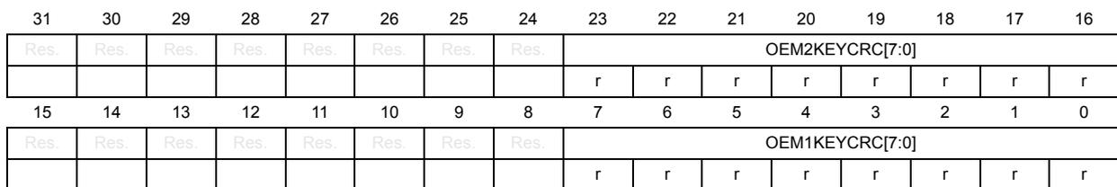
| 31 | 30 | 29 | 28 | 27 | 26 | 25 | 24 | 23 | 22 | 21 | 20 | 19 | 18 | 17 | 16 |
| Res. | Res. | Res. | Res. | Res. | Res. | Res. | Res. | OEM2KEYCRC[7:0] | |||||||
| r | r | r | r | r | r | r | r | ||||||||
| 15 | 14 | 13 | 12 | 11 | 10 | 9 | 8 | 7 | 6 | 5 | 4 | 3 | 2 | 1 | 0 |
| Res. | Res. | Res. | Res. | Res. | Res. | Res. | Res. | OEM1KEYCRC[7:0] | |||||||
| r | r | r | r | r | r | r | r | ||||||||
Bits 31:24 Reserved, must be kept at reset value.
Bits 23:16 OEM2KEYCRC[7:0] : 8-bit OEM2KEY CRC
CRC is automatically computed by hardware while loading the OEM2KEYkey. The CRC computation is an 8-bit checksum using the standard CRC-8-CCITT algorithm \( X^8 + X^2 + X + 1 \) (according to the convention). Source code is available in OEM Key CRC source .
Note: CRC information is updated each time FLASH OEM2KEY registers are written
Bits 15:8 Reserved, must be kept at reset value.
Bits 7:0 OEM1KEYCRC[7:0] : 8-bit OEMKEY1 CRC
CRC is automatically computed by hardware while loading the OEM1KEY key. The CRC computation is an 8-bit checksum using the standard CRC-8-CCITT algorithm \( X^8 + X^2 + X + 1 \) (according the convention). Source code is available in OEM Key CRC source .
Note: CRC information is updated each time FLASH OEM1KEY registers are written
7.10.43 FLASH register map
Table 73. FLASH register map and reset values
| Offset | Register name | 31 | 30 | 29 | 28 | 27 | 26 | 25 | 24 | 23 | 22 | 21 | 20 | 19 | 18 | 17 | 16 | 15 | 14 | 13 | 12 | 11 | 10 | 9 | 8 | 7 | 6 | 5 | 4 | 3 | 2 | 1 | 0 |
|---|---|---|---|---|---|---|---|---|---|---|---|---|---|---|---|---|---|---|---|---|---|---|---|---|---|---|---|---|---|---|---|---|---|
| 0x00 | FLASH_ACR | Res. | Res. | Res. | Res. | Res. | Res. | Res. | Res. | Res. | Res. | Res. | Res. | Res. | Res. | Res. | Res. | Res. | SLEEP_PD | PDREQ2 | PDREQ1 | LPM | Res. | Res. | PRFTEN | Res. | Res. | Res. | Res. | LATENCY [3:0] | |||
| Reset value | 0 | 0 | 0 | 0 | 0 | 0 | 0 | 0 | 1 | ||||||||||||||||||||||||
| 0x04 | Reserved | Reserved | |||||||||||||||||||||||||||||||
| 0x08 | FLASH_KEYR | KEY[31:0] | |||||||||||||||||||||||||||||||
| Reset value | 0 | 0 | 0 | 0 | 0 | 0 | 0 | 0 | 0 | 0 | 0 | 0 | 0 | 0 | 0 | 0 | 0 | 0 | 0 | 0 | 0 | 0 | 0 | 0 | 0 | 0 | 0 | 0 | 0 | 0 | 0 | 0 | |
| 0x0C | FLASH_SKEYR | KEY[31:0] | |||||||||||||||||||||||||||||||
| Reset value | 0 | 0 | 0 | 0 | 0 | 0 | 0 | 0 | 0 | 0 | 0 | 0 | 0 | 0 | 0 | 0 | 0 | 0 | 0 | 0 | 0 | 0 | 0 | 0 | 0 | 0 | 0 | 0 | 0 | 0 | 0 | 0 | |
| 0x10 | FLASH_OPT-KEYR | KEY[31:0] | |||||||||||||||||||||||||||||||
| Reset value | 0 | 0 | 0 | 0 | 0 | 0 | 0 | 0 | 0 | 0 | 0 | 0 | 0 | 0 | 0 | 0 | 0 | 0 | 0 | 0 | 0 | 0 | 0 | 0 | 0 | 0 | 0 | 0 | 0 | 0 | 0 | 0 | |
| 0x14 | Reserved | Reserved | |||||||||||||||||||||||||||||||
| 0x18 | FLASH_PD-KEY1R | KEY1[31:0] | |||||||||||||||||||||||||||||||
| Reset value | 0 | 0 | 0 | 0 | 0 | 0 | 0 | 0 | 0 | 0 | 0 | 0 | 0 | 0 | 0 | 0 | 0 | 0 | 0 | 0 | 0 | 0 | 0 | 0 | 0 | 0 | 0 | 0 | 0 | 0 | 0 | 0 | |
| 0x1C | FLASH_PD-KEY2R | KEY2[31:0] | |||||||||||||||||||||||||||||||
| Reset value | 0 | 0 | 0 | 0 | 0 | 0 | 0 | 0 | 0 | 0 | 0 | 0 | 0 | 0 | 0 | 0 | 0 | 0 | 0 | 0 | 0 | 0 | 0 | 0 | 0 | 0 | 0 | 0 | 0 | 0 | 0 | 0 | |
| 0x20 | FLASH_SR | Res. | Res. | Res. | Res. | Res. | Res. | Res. | Res. | Res. | Res. | PD2 | PD1 | OEM2LOCK | OEM1LOCK | WDW | BSY | Res. | Res. | OPTWERR | Res. | Res. | Res. | Res. | Res. | PGSERR | SIZERR | PGAERR | WRPERR | PROGERR | Res. | OPERR | EOP |
| Reset value | 0 | 0 | X | X | X | X | 0 | 0 | 0 | 0 | 0 | 0 | 0 | 0 | |||||||||||||||||||
| 0x24 | FLASH_SSR | Res. | Res. | Res. | Res. | Res. | Res. | Res. | Res. | Res. | Res. | Res. | Res. | Res. | Res. | WDW | BSY | Res. | Res. | Res. | Res. | Res. | Res. | Res. | Res. | PGSERR | SIZERR | PGAERR | WRPERR | PROGERR | Res. | OPERR | EOP |
| Reset value | 0 | 0 | 0 | 0 | 0 | 0 | 0 | 0 | 0 | ||||||||||||||||||||||||
| 0x28 | FLASH_CR | LOCK | OPTLOCK | Res. | Res. | OBL_LAUNCH | Res. | ERRIE | EOPIE | Res. | Res. | Res. | Res. | Res. | Res. | OPTSTRT | STRT | MER2 | BWR | Res. | Res. | BKER | PNB[7:0] | MER1 | PER | PG | |||||||
| Reset value | 1 | 1 | 0 | 0 | 0 | 0 | 0 | 0 | 0 | 0 | 0 | 0 | 0 | 0 | 0 | 0 | 0 | 0 | 0 | 0 | |||||||||||||
| 0x2C | FLASH_SCR | LOCK | Res. | INV | Res. | Res. | Res. | ERRIE | EOPIE | Res. | Res. | Res. | Res. | Res. | Res. | Res. | STRT | MER2 | BWR | Res. | Res. | BKER | PNB[7:0] | MER1 | PER | PG | |||||||
| Reset value | 1 | 0 | 0 | 0 | 0 | 0 | 0 | 0 | 0 | 0 | 0 | 0 | 0 | 0 | 0 | 0 | 0 | 0 | |||||||||||||||
Table 73. FLASH register map and reset values (continued)
| Offset | Register name | 31 | 30 | 29 | 28 | 27 | 26 | 25 | 24 | 23 | 22 | 21 | 20 | 19 | 18 | 17 | 16 | 15 | 14 | 13 | 12 | 11 | 10 | 9 | 8 | 7 | 6 | 5 | 4 | 3 | 2 | 1 | 0 |
|---|---|---|---|---|---|---|---|---|---|---|---|---|---|---|---|---|---|---|---|---|---|---|---|---|---|---|---|---|---|---|---|---|---|
| 0x30 | FLASH_EC-CCORR | Res. | ECCC | Res. | Res. | Res. | Res. | Res. | ECCIE | Res. | SYSF_ECC | BK_ECC | Res. | ADDR_ECC[19:0] | |||||||||||||||||||
| Reset value | 0 | 0 | 0 | 0 | 0 | 0 | 0 | 0 | 0 | 0 | 0 | 0 | 0 | 0 | 0 | 0 | 0 | 0 | 0 | 0 | 0 | 0 | 0 | 0 | |||||||||
| 0x34 | FLASH_EC-CDETR | ECCD | Res. | Res. | Res. | Res. | Res. | Res. | Res. | Res. | SYSF_ECC | BK_ECC | Res. | ADDR_ECC[19:0] | |||||||||||||||||||
| Reset value | 0 | 0 | 0 | 0 | 0 | 0 | 0 | 0 | 0 | 0 | 0 | 0 | 0 | 0 | 0 | 0 | 0 | 0 | 0 | 0 | 0 | 0 | 0 | ||||||||||
| 0x38 | FLASH_OPSR | CODE_OP[2:0] | Res. | Res. | Res. | Res. | Res. | Res. | SYSF_OP | BK_OP | Res. | ADDR_OP[19:0] | |||||||||||||||||||||
| Reset value | X | X | X | X | X | X | X | X | X | X | X | X | X | X | X | X | X | X | X | X | X | X | X | X | X | ||||||||
| 0x3C | Reserved | Reserved | |||||||||||||||||||||||||||||||
| 0x40 | FLASH_OPTR | TZEN | IO_VDDIO2_HSLV | IO_VDD_HSLV | Res. | NBOOT0 | NSWBOOT0 | SRAM2_RST | SRAM2_PE | SRAM3_PE | Res. | DUALBANK | SWAP_BANK | WWDG_SW | IWDG_STDBY | IWDG_STOP | IWDG_SW | SRAM1_RST | NRST_SHDW | NRST_STDBY | NRST_STOP | BDRST_POR | BOR_LEV[2:0] | RDP[7:0] | |||||||||
| Reset value | X | X | X | X | X | X | X | X | X | X | X | X | X | X | X | X | X | X | X | X | X | X | X | X | X | X | X | X | X | X | |||
| 0x40 | FLASH_OPTR [alternate] STM32U375/385 only | TZEN | IO_VDDIO2_HSLV | IO_VDD_HSLV | Res. | NBOOT0 | NSWBOOT0 | SRAM2_RST | SRAM2_PE | BL_IO_VDDIO2_HSLV[1:0] | DUALBANK | SWAP_BANK | WWDG_SW | IWDG_STDBY | IWDG_STOP | IWDG_SW | SRAM1_RST | NRST_SHDW | NRST_STDBY | NRST_STOP | BDRST_POR | BOR_LEV[2:0] | RDP[7:0] | ||||||||||
| Reset value | X | X | X | X | X | X | X | X | X | X | X | X | X | X | X | X | X | X | X | X | X | X | X | X | X | X | X | X | X | X | X | ||
| 0x44 | FLASH_BOOT0R | ADD[24:0] | Res. | Res. | Res. | Res. | Res. | Res. | Res. | ||||||||||||||||||||||||
| Reset value | X | X | X | X | X | X | X | X | X | X | X | X | X | X | X | X | X | X | X | X | X | X | X | X | X | ||||||||
| 0x48 | FLASH_BOOT1R | ADD[24:0] | Res. | Res. | Res. | Res. | Res. | Res. | Res. | ||||||||||||||||||||||||
| Reset value | X | X | X | X | X | X | X | X | X | X | X | X | X | X | X | X | X | X | X | X | X | X | X | X | X | ||||||||
| 0x4C | FLASH_S-BOOT0R | ADD[24:0] | Res. | Res. | Res. | Res. | Res. | Res. | BOOT_LOCK | ||||||||||||||||||||||||
| Reset value | X | X | X | X | X | X | X | X | X | X | X | X | X | X | X | X | X | X | X | X | X | X | X | X | X | X | |||||||
| 0x50 | FLASH_SECWM1_R1 | Res. | Res. | Res. | Res. | Res. | Res. | Res. | Res. | SECWM1_END[7:0] | Res. | Res. | Res. | Res. | Res. | Res. | Res. | Res. | SECWM1_STRT[7:0] | ||||||||||||||
| Reset value | X | X | X | X | X | X | X | X | X | X | X | X | X | X | X | X | |||||||||||||||||
| 0x54 | FLASH_SECWM1_R2 | HDP1EN[7:0] | HDP1_END[7:0] | Res. | Res. | Res. | Res. | Res. | Res. | Res. | Res. | Res. | Res. | Res. | Res. | Res. | Res. | Res. | Res. | ||||||||||||||
| Reset value | X | X | X | X | X | X | X | X | X | X | X | X | X | X | X | X | |||||||||||||||||
| Offset | Register name | 31 | 30 | 29 | 28 | 27 | 26 | 25 | 24 | 23 | 22 | 21 | 20 | 19 | 18 | 17 | 16 | 15 | 14 | 13 | 12 | 11 | 10 | 9 | 8 | 7 | 6 | 5 | 4 | 3 | 2 | 1 | 0 |
|---|---|---|---|---|---|---|---|---|---|---|---|---|---|---|---|---|---|---|---|---|---|---|---|---|---|---|---|---|---|---|---|---|---|
| 0x58 | FLASH_WRP1AR | UNLOCK | Res. | Res. | Res. | Res. | Res. | Res. | Res. | END[7:0] | Res. | Res. | Res. | Res. | Res. | Res. | Res. | Res. | STRT[7:0] | ||||||||||||||
| Reset value | X | X | X | X | X | X | X | X | X | X | X | X | X | X | X | X | X | ||||||||||||||||
| 0x5C | FLASH_WRP1BR | UNLOCK | Res. | Res. | Res. | Res. | Res. | Res. | Res. | END[7:0] | Res. | Res. | Res. | Res. | Res. | Res. | Res. | Res. | STRT[7:0] | ||||||||||||||
| Reset value | X | X | X | X | X | X | X | X | X | X | X | X | X | X | X | X | X | ||||||||||||||||
| 0x60 | FLASH_SECWM2_R1 | Res. | Res. | Res. | Res. | Res. | Res. | Res. | Res. | SECWM2_END[7:0] | Res. | Res. | Res. | Res. | Res. | Res. | Res. | Res. | SECWM2_STRT[7:0] | ||||||||||||||
| Reset value | X | X | X | X | X | X | X | X | X | X | X | X | X | X | X | X | |||||||||||||||||
| 0x64 | FLASH_SECWM2_R2 | HDP2EN[7:0] | HDP2_END[7:0] | Res. | Res. | Res. | Res. | Res. | Res. | Res. | Res. | Res. | Res. | Res. | Res. | Res. | Res. | Res. | Res. | ||||||||||||||
| Reset value | X | X | X | X | X | X | X | X | X | X | X | X | X | X | X | X | |||||||||||||||||
| 0x68 | FLASH_WRP2AR | UNLOCK | Res. | Res. | Res. | Res. | Res. | Res. | Res. | END[7:0] | Res. | Res. | Res. | Res. | Res. | Res. | Res. | Res. | STRT[7:0] | ||||||||||||||
| Reset value | X | X | X | X | X | X | X | X | X | X | X | X | X | X | X | X | X | ||||||||||||||||
| 0x6C | FLASH_WRP2BR | UNLOCK | Res. | Res. | Res. | Res. | Res. | Res. | Res. | END[7:0] | Res. | Res. | Res. | Res. | Res. | Res. | Res. | Res. | STRT[7:0] | ||||||||||||||
| Reset value | X | X | X | X | X | X | X | X | X | X | X | X | X | X | X | X | X | ||||||||||||||||
| 0x70-0x7C | Reserved | Reserved | |||||||||||||||||||||||||||||||
| 0x80+ 0x4 * (x - 1), (x=1 to 8) | FLASH_SECB1B_Rx | SEC31 | SEC30 | SEC29 | SEC28 | SEC27 | SEC26 | SEC25 | SEC24 | SEC23 | SEC22 | SEC21 | SEC20 | SEC19 | SEC18 | SEC17 | SEC16 | SEC15 | SEC14 | SEC13 | SEC12 | SEC11 | SEC10 | SEC9 | SEC8 | SEC7 | SEC6 | SEC5 | SEC4 | SEC3 | SEC2 | SEC1 | SEC0 |
| Reset value | 0 | 0 | 0 | 0 | 0 | 0 | 0 | 0 | 0 | 0 | 0 | 0 | 0 | 0 | 0 | 0 | 0 | 0 | 0 | 0 | 0 | 0 | 0 | 0 | 0 | 0 | 0 | 0 | 0 | 0 | 0 | 0 | |
| 0xA0+ 0x4 * (x - 1), (x=1 to 8) | FLASH_SECB2_Rx | SEC31 | SEC30 | SEC29 | SEC28 | SEC27 | SEC26 | SEC25 | SEC24 | SEC23 | SEC22 | SEC21 | SEC20 | SEC19 | SEC18 | SEC17 | SEC16 | SEC15 | SEC14 | SEC13 | SEC12 | SEC11 | SEC10 | SEC9 | SEC8 | SEC7 | SEC6 | SEC5 | SEC4 | SEC3 | SEC2 | SEC1 | SEC0 |
| Reset value | 0 | 0 | 0 | 0 | 0 | 0 | 0 | 0 | 0 | 0 | 0 | 0 | 0 | 0 | 0 | 0 | 0 | 0 | 0 | 0 | 0 | 0 | 0 | 0 | 0 | 0 | 0 | 0 | 0 | 0 | 0 | 0 | |
| 0xC0 | FLASH_SECHD_PCR | HDP2EXT_ACCDIS[7:0] | HDP1EXT_ACCDIS[7:0] | HDP2_ACCDIS[7:0] | HDP1_ACCDIS[7:0] | ||||||||||||||||||||||||||||
| Reset value | 1 | 0 | 1 | 0 | 0 | 0 | 1 | 1 | 1 | 0 | 1 | 0 | 0 | 0 | 1 | 1 | 1 | 0 | 1 | 0 | 0 | 0 | 1 | 1 | 1 | 0 | 1 | 0 | 0 | 0 | 1 | 1 | |
| 0xC4 | FLASH_PRIVCFG_R | Res. | Res. | Res. | Res. | Res. | Res. | Res. | Res. | Res. | Res. | Res. | Res. | Res. | Res. | Res. | Res. | Res. | Res. | Res. | Res. | Res. | Res. | Res. | Res. | Res. | Res. | Res. | Res. | Res. | Res. | PRIV | SPRIV |
| Reset value | 0 | 0 | |||||||||||||||||||||||||||||||
| 0xC8 | FLASH_SECHD_PEXTR | Res. | Res. | Res. | Res. | Res. | Res. | HDP2_EXT[8:0] | Res. | Res. | Res. | Res. | Res. | Res. | Res. | HDP1_EXT[8:0] | |||||||||||||||||
| Reset value | 0 | 0 | 0 | 0 | 0 | 0 | 0 | 0 | 0 | 0 | 0 | 0 | 0 | 0 | 0 | 0 | 0 | 0 | |||||||||||||||
| 0xCC | Reserved | Reserved | |||||||||||||||||||||||||||||||
| 0xD0+ 0x4 * (x - 1), (x=1 to 8) | FLASH_PRIVBB1_Rx | PRIV31 | PRIV30 | PRIV29 | PRIV28 | PRIV27 | PRIV26 | PRIV25 | PRIV24 | PRIV23 | PRIV22 | PRIV21 | PRIV20 | PRIV19 | PRIV18 | PRIV17 | PRIV16 | PRIV15 | PRIV14 | PRIV13 | PRIV12 | PRIV11 | PRIV10 | PRIV9 | PRIV8 | PRIV7 | PRIV6 | PRIV5 | PRIV4 | PRIV3 | PRIV2 | PRIV1 | PRIV0 |
| Reset value | 0 | 0 | 0 | 0 | 0 | 0 | 0 | 0 | 0 | 0 | 0 | 0 | 0 | 0 | 0 | 0 | 0 | 0 | 0 | 0 | 0 | 0 | 0 | 0 | 0 | 0 | 0 | 0 | 0 | 0 | 0 | 0 | |
| 0xF0+ 0x4 * (x - 1), (x=1 to 8) | FLASH_PRIVBB2_Rx | PRIV31 | PRIV30 | PRIV29 | PRIV28 | PRIV27 | PRIV26 | PRIV25 | PRIV24 | PRIV23 | PRIV22 | PRIV21 | PRIV20 | PRIV19 | PRIV18 | PRIV17 | PRIV16 | PRIV15 | PRIV14 | PRIV13 | PRIV12 | PRIV11 | PRIV10 | PRIV9 | PRIV8 | PRIV7 | PRIV6 | PRIV5 | PRIV4 | PRIV3 | PRIV2 | PRIV1 | PRIV0 |
| Reset value | 0 | 0 | 0 | 0 | 0 | 0 | 0 | 0 | 0 | 0 | 0 | 0 | 0 | 0 | 0 | 0 | 0 | 0 | 0 | 0 | 0 | 0 | 0 | 0 | 0 | 0 | 0 | 0 | 0 | 0 | 0 | 0 | |
Table 73. FLASH register map and reset values (continued)
| Offset | Register name | 31 | 30 | 29 | 28 | 27 | 26 | 25 | 24 | 23 | 22 | 21 | 20 | 19 | 18 | 17 | 16 | 15 | 14 | 13 | 12 | 11 | 10 | 9 | 8 | 7 | 6 | 5 | 4 | 3 | 2 | 1 | 0 |
|---|---|---|---|---|---|---|---|---|---|---|---|---|---|---|---|---|---|---|---|---|---|---|---|---|---|---|---|---|---|---|---|---|---|
| 0x110 | FLASH_O-EM1KEYR1 | OEM1KEY[31:0] | |||||||||||||||||||||||||||||||
| Reset value | 0 | 0 | 0 | 0 | 0 | 0 | 0 | 0 | 0 | 0 | 0 | 0 | 0 | 0 | 0 | 0 | 0 | 0 | 0 | 0 | 0 | 0 | 0 | 0 | 0 | 0 | 0 | 0 | 0 | 0 | 0 | 0 | |
| 0x114 | FLASH_O-EM1KEYR2 | OEM1KEY[63:32] | |||||||||||||||||||||||||||||||
| Reset value | 0 | 0 | 0 | 0 | 0 | 0 | 0 | 0 | 0 | 0 | 0 | 0 | 0 | 0 | 0 | 0 | 0 | 0 | 0 | 0 | 0 | 0 | 0 | 0 | 0 | 0 | 0 | 0 | 0 | 0 | 0 | 0 | |
| 0x118 | FLASH_O-EM1KEYR3 | OEM1KEY[95:64] | |||||||||||||||||||||||||||||||
| Reset value | 0 | 0 | 0 | 0 | 0 | 0 | 0 | 0 | 0 | 0 | 0 | 0 | 0 | 0 | 0 | 0 | 0 | 0 | 0 | 0 | 0 | 0 | 0 | 0 | 0 | 0 | 0 | 0 | 0 | 0 | 0 | 0 | |
| 0x11C | FLASH_O-EM1KEYR4 | OEM1KEY[127:96] | |||||||||||||||||||||||||||||||
| Reset value | 0 | 0 | 0 | 0 | 0 | 0 | 0 | 0 | 0 | 0 | 0 | 0 | 0 | 0 | 0 | 0 | 0 | 0 | 0 | 0 | 0 | 0 | 0 | 0 | 0 | 0 | 0 | 0 | 0 | 0 | 0 | 0 | |
| 0x120 | FLASH_O-EM2KEYR1 | OEM2KEY[31:0] | |||||||||||||||||||||||||||||||
| Reset value | 0 | 0 | 0 | 0 | 0 | 0 | 0 | 0 | 0 | 0 | 0 | 0 | 0 | 0 | 0 | 0 | 0 | 0 | 0 | 0 | 0 | 0 | 0 | 0 | 0 | 0 | 0 | 0 | 0 | 0 | 0 | 0 | |
| 0x124 | FLASH_O-EM2KEYR2 | OEM2KEY[63:32] | |||||||||||||||||||||||||||||||
| Reset value | 0 | 0 | 0 | 0 | 0 | 0 | 0 | 0 | 0 | 0 | 0 | 0 | 0 | 0 | 0 | 0 | 0 | 0 | 0 | 0 | 0 | 0 | 0 | 0 | 0 | 0 | 0 | 0 | 0 | 0 | 0 | 0 | |
| 0x128 | FLASH_O-EM2KEYR3 | OEM2KEY[95:64] | |||||||||||||||||||||||||||||||
| Reset value | 0 | 0 | 0 | 0 | 0 | 0 | 0 | 0 | 0 | 0 | 0 | 0 | 0 | 0 | 0 | 0 | 0 | 0 | 0 | 0 | 0 | 0 | 0 | 0 | 0 | 0 | 0 | 0 | 0 | 0 | 0 | 0 | |
| 0x12C | FLASH_O-EM2KEYR4 | OEM2KEY[127:96] | |||||||||||||||||||||||||||||||
| Reset value | 0 | 0 | 0 | 0 | 0 | 0 | 0 | 0 | 0 | 0 | 0 | 0 | 0 | 0 | 0 | 0 | 0 | 0 | 0 | 0 | 0 | 0 | 0 | 0 | 0 | 0 | 0 | 0 | 0 | 0 | 0 | 0 | |
| 0x130 | FLASH_OEM-KEYSR | Res | Res | Res | Res | Res | Res | Res | Res | OEM2KEYCRC[7:0] | Res | Res | Res | Res | Res | Res | Res | Res | OEM1KEYCRC[7:0] | ||||||||||||||
| Reset value | 0 | 0 | 0 | 0 | 0 | 0 | 0 | 0 | 0 | 0 | 0 | 0 | 0 | 0 | 0 | 0 | |||||||||||||||||
Refer to Section 2.3: Memory organization for the register boundary addresses.