6. RAM configuration controller (RAMCFG)
6.1 RAMCFG introduction
The RAMCFG configures the features of the internal SRAMs (SRAM1, SRAM2 and SRAM3).
On STM32U3B5/3C5, RAMCFG does not support any SRAM4 feature.
6.2 RAMCFG main features
The internal SRAM supports some of the features listed hereafter, configured in RAMCFG:
- • Parity check on SRAM2 and SRAM3
- • Write protection (1-Kbyte granularity) on SRAM2
- • SRAM software erase
6.3 RAMCFG functional description
6.3.1 Internal SRAMs features
The STM32U3 devices feature up to four contiguous SRAMs.
Table 35. SRAM structure
| SRAM | STM32U356/366 | STM32U375/385 | STM32U3B5/3C5 |
|---|---|---|---|
| SRAM1 | 128 Kbytes | 192 Kbytes | |
| SRAM2 | 64 Kbytes | ||
| SRAM3 | - | - | 320 Kbytes |
| SRAM4 | - | - | 64 Kbytes |
- • Each SRAM is composed of several blocks of different sizes, which can be independently powered down or retained in Stop mode based on application requirements. Only SRAM2 can be fully or partially retained in Standby mode. Refer to the power controller (PWR) for more details.
- • All internal SRAMs but SRAM4 are erased by hardware in case of Readout protection (RDP) level regression to level 0.5 or level 0. Refer to Section 7.6.2: Readout protection (RDP) for more details.
- • Both SRAM1, SRAM2 and SRAM3 are erased when a system reset occurs if the corresponding SRAMx_RST option bit is selected in the flash memory user option bytes. Refer to Section 7.4: FLASH option bytes for more details.
- • SRAM2 is protected by the tamper detection circuit, and is erased by hardware in case of tamper detection. Refer to Section 47: Tamper and backup registers (TAMP) for more details.
- • The RAMCFG embeds the registers related to the internal SRAMs parity check, write protection and software erase.
- • Parity check can be enabled for SRAM2 and SRAM3.
- • Both SRAM1, SRAM2 and SRAM3 can be erased by software.
- • Write protection can be set on SRAM2, with 1-Kbyte granularity.
The table below summarizes the features supported by each internal SRAM.
Table 36. Internal SRAM features
| SRAM feature | SRAM1 | SRAM2 | SRAM3 | SRAM4 |
|---|---|---|---|---|
| Optional retention in Standby mode | - | X | - | - |
| Erased with RDP regression | X | X | X | - |
| Erased or blocked by tamper detection | - | X | - | - |
| Optionally erased with system reset | X | X | X | - |
| Software erase | X | X | X | - |
| Parity check | - | X | X | - |
| Write protection | - | X | - | - |
6.3.2 Parity error detection (SRAM2/3)
The parity error is supported by SRAM2 and SRAM3. For each word, 4 bits are used for parity check (1 bit per byte) in order to increase memory robustness, as required for instance by Class B or SIL norms.
Parity can be controlled through PCE bit (RAMCFG_MxCR) and RAMCFG_MxPARKEYR:
- • To enable parity: if parity is disabled, enable it by setting PCE bit.
- • To disable parity: if parity is enabled, disable it with the following sequence:
- – Write 0xAE into PARKEY[7:0] (RAMCFG_MxPARKEYR).
- – Write 0x75 into PARKEY[7:0] (RAMCFG_MxPARKEYR).
- – Write 0 into PCE bit (1 to 0 transition is possible only if PARKEY[7:0] is unlocked).
When parity is enabled by SRAMx_PE user option bit, the PCE bit is automatically set (in RAMCFG_MxCR) after system reset. Refer to Section 7.4: FLASH option bytes for more details.
An interrupt or NMI is generated if enabled by the PEIE or PENMI bit in RAMCFG_MxIER. The failing address is stored in the PEA[31:0] in RAMCFG_MxPEAR if the ALE bit is set in RAMCFG_MxCR.
The parity error triggers a system break event in TIM1/8/15/16/17, if the SPL bit is set in SYSCFG_CFGR2.
6.3.3 Write protection (SRAM2)
The SRAM2 is made of 64 1-Kbyte pages. Each 1-Kbyte page can be write-protected by setting its corresponding PxWP (x = 0 to 63) bit in the RAMCFG_M2WPRx.
6.3.4 Software erase
SRAM erase can be requested by executing this software sequence:
- 1. Write 0xCA in RAMCFG_MxERKEYR.
- 2. Write 0x53 in RAMCFG_MxERKEYR.
- 3. Write 1 to the SRAMER bit in RAMCFG_MxCR.
SRAMBUSY flag is set in the related SRAM interrupt status register as long as the erase is ongoing.
The total duration of each SRAM erase is N AHB clock cycles, where N is the size of the SRAM in 32-bit words.
If the SRAM is written while an erase is ongoing, wait states are inserted on the AHB bus until the end of the erase operation. The SRAM is read as zero while an erase is ongoing.
6.4 RAMCFG in low-power modes
Table 37. Effect of low-power modes on RAMCFG
| Mode | Description |
|---|---|
| Sleep | No effect. RAMCFG interrupts cause the device to exit the sleep mode. |
| Stop | The content of RAMCFG registers is kept. The parity check on SRAM2/3 is functional and parity error interrupt or NMI causes the device to exit from Stop 0, Stop1 and Stop 2 modes. |
| Standby | The RAMCFG peripheral is powered down and must be reinitialized after exiting Standby. |
6.5 RAMCFG interrupts
The table below gives the list of RAMCFG interrupt requests.
Table 38. RAMCFG interrupt requests
| Interrupt acronym | Interrupt event | Event flag | Enable control bit | Interrupt clear method | Exit Sleep mode | Exit Stop modes | Exit Standby mode |
|---|---|---|---|---|---|---|---|
| RAMCFG | Parity error | PED | PEIE = 1 and PENMI = 0 | Write 1 in CPED | Yes | Yes (1) | No |
| NMI | Parity error | PED | PENMI | Write 1 in CPED | Yes | Yes (1) | No |
1. Stop 0, Stop 1, and Stop 2 modes only.
6.6 RAMCFG registers
In registers described below, x refers to SRAM1/2/3 when x = 1, 2 or 3 respectively.
SRAM3 is only available on STM32U3B5/3C5
6.6.1 RAMCFG memory x control register (RAMCFG_MxCR)
Address offset: 0x40 * (x - 1), (x = 1 to 3)
Reset value: 0x0000 000X
| 31 | 30 | 29 | 28 | 27 | 26 | 25 | 24 | 23 | 22 | 21 | 20 | 19 | 18 | 17 | 16 |
|---|---|---|---|---|---|---|---|---|---|---|---|---|---|---|---|
| Res. | Res. | Res. | Res. | Res. | Res. | Res. | Res. | Res. | Res. | Res. | Res. | Res. | Res. | Res. | Res. |
| 15 | 14 | 13 | 12 | 11 | 10 | 9 | 8 | 7 | 6 | 5 | 4 | 3 | 2 | 1 | 0 |
| Res. | Res. | Res. | Res. | Res. | Res. | Res. | SRAM ER | Res. | Res. | Res. | ALE | Res. | Res. | Res. | PCE |
| rs | rw | rw |
Bits 31:9 Reserved, must be kept at reset value.
Bit 8 SRAMER : SRAM erase
This bit can be set by software only after writing the unlock sequence in the ERASEKEY bitfield of RAMCFG_MxERKEYR. Setting this bit starts the SRAM erase. This bit is automatically cleared by hardware at the end of the erase operation.
0: No erase operation ongoing
1: Erase operation ongoing
Bits 7:5 Reserved, must be kept at reset value.
Bit 4 ALE : Address latch enable in case of parity error
0: Failing address not stored in the SRAMx parity error address registers
1: Failing address stored in the SRAMx parity error address registers
Note: This bit is reserved and must be kept at reset value in SRAM1 control registers.
Bits 3:1 Reserved, must be kept at reset value.
Bit 0 PCE : Parity check enable
This bit reset value is defined by the user option bit configuration. When set, this bit can be cleared by software only after writing the unlock sequence in RAMCFG_M2PARKEYR.
0: Parity check disabled
1: Parity check enabled
Note: This bit is reserved and must be kept at reset value in SRAM1 control registers.
6.6.2 RAMCFG memory x interrupt enable register (RAMCFG_MxIER)
Address offset: \( 0x04 + 0x40 * (x - 1) \) , ( \( x = 2 \) to \( 3 \) )
Reset value: 0x0000 0000
| 31 | 30 | 29 | 28 | 27 | 26 | 25 | 24 | 23 | 22 | 21 | 20 | 19 | 18 | 17 | 16 |
|---|---|---|---|---|---|---|---|---|---|---|---|---|---|---|---|
| Res. | Res. | Res. | Res. | Res. | Res. | Res. | Res. | Res. | Res. | Res. | Res. | Res. | Res. | Res. | Res. |
| 15 | 14 | 13 | 12 | 11 | 10 | 9 | 8 | 7 | 6 | 5 | 4 | 3 | 2 | 1 | 0 |
| Res. | Res. | Res. | Res. | Res. | Res. | Res. | Res. | Res. | Res. | Res. | Res. | PENMI | Res. | Res. | PEIE |
| rs | nw |
Bits 31:4 Reserved, must be kept at reset value.
Bit 3 PENMI : Parity error NMI
This bit is set by software and cleared only by a global RAMCFG reset.
0: NMI not generated in case of Parity error
1: NMI generated in case of Parity error
Note: If this bit is set, the RAMCFG maskable interrupt is not generated whatever PEIE value.
Bits 2:1 Reserved, must be kept at reset value.
Bit 0 PEIE : Parity error interrupt enable
0: Parity error interrupt disabled
1: Parity error interrupt enabled
6.6.3 RAMCFG memory x interrupt status register (RAMCFG_MxISR)
Address offset: \( 0x08 + 0x40 * (x - 1) \) , ( \( x = 1 \) to \( 3 \) )
Reset value: 0x0000 0000
| 31 | 30 | 29 | 28 | 27 | 26 | 25 | 24 | 23 | 22 | 21 | 20 | 19 | 18 | 17 | 16 |
|---|---|---|---|---|---|---|---|---|---|---|---|---|---|---|---|
| Res. | Res. | Res. | Res. | Res. | Res. | Res. | Res. | Res. | Res. | Res. | Res. | Res. | Res. | Res. | Res. |
| 15 | 14 | 13 | 12 | 11 | 10 | 9 | 8 | 7 | 6 | 5 | 4 | 3 | 2 | 1 | 0 |
| Res. | Res. | Res. | Res. | Res. | Res. | Res. | SRAM BUSY | Res. | Res. | Res. | Res. | Res. | Res. | PED | Res. |
| r | r |
Bits 31:9 Reserved, must be kept at reset value.
Bit 8 SRAMBUSY : SRAM busy with erase operation
0: No erase operation ongoing
1: Erase operation ongoing
Bits 7:2 Reserved, must be kept at reset value.
Bit 1 PED : Parity error detected
0: No Parity error detected
1: Parity error detected
Note: This bit is reserved and must be kept at reset value in SRAM1 control registers.
Bit 0 Reserved, must be kept at reset value.
6.6.4 RAMCFG memory x parity error address register (RAMCFG_MxPEAR)
Address offset: \( 0x10 + 0x40 \times (x - 1) \) , ( \( x = 2 \) to \( 3 \) )
Reset value: 0x0000 0000
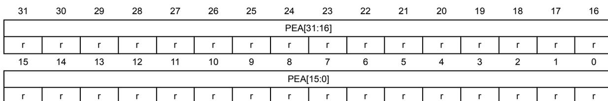
| 31 | 30 | 29 | 28 | 27 | 26 | 25 | 24 | 23 | 22 | 21 | 20 | 19 | 18 | 17 | 16 |
| PEA[31:16] | |||||||||||||||
| r | r | r | r | r | r | r | r | r | r | r | r | r | r | r | r |
| 15 | 14 | 13 | 12 | 11 | 10 | 9 | 8 | 7 | 6 | 5 | 4 | 3 | 2 | 1 | 0 |
| PEA[15:0] | |||||||||||||||
| r | r | r | r | r | r | r | r | r | r | r | r | r | r | r | r |
Bits 31:0 PEA[31:0] : Parity error address
When the ALE bit is set in RAMCFG_MxCR, this bitfield is updated with the address corresponding to the parity error.
6.6.5 RAMCFG memory x interrupt clear register (RAMCFG_MxICR)
Address offset: \( 0x14 + 0x40 \times (x - 1) \) , ( \( x = 2 \) to \( 3 \) )
Reset value: 0x0000 0000
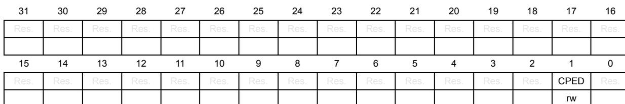
| 31 | 30 | 29 | 28 | 27 | 26 | 25 | 24 | 23 | 22 | 21 | 20 | 19 | 18 | 17 | 16 |
| Res. | Res. | Res. | Res. | Res. | Res. | Res. | Res. | Res. | Res. | Res. | Res. | Res. | Res. | Res. | Res. |
| 15 | 14 | 13 | 12 | 11 | 10 | 9 | 8 | 7 | 6 | 5 | 4 | 3 | 2 | 1 | 0 |
| Res. | Res. | Res. | Res. | Res. | Res. | Res. | Res. | Res. | Res. | Res. | Res. | Res. | Res. | CPED | Res. |
| rw |
Bits 31:2 Reserved, must be kept at reset value.
Bit 1 CPED : Clear parity error detected
Writing 1 to this flag clears PED bit in RAMCFG_MxISR. Reading this flag returns the PED value.
Bit 0 Reserved, must be kept at reset value.
6.6.6 RAMCFG memory 2 write protection register 1 (RAMCFG_M2WPR1)
Address offset: 0x058
Reset value: 0x0000 0000
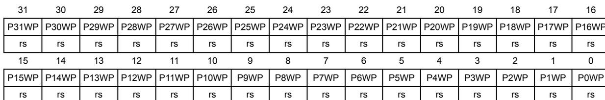
| 31 | 30 | 29 | 28 | 27 | 26 | 25 | 24 | 23 | 22 | 21 | 20 | 19 | 18 | 17 | 16 |
| P31WP | P30WP | P29WP | P28WP | P27WP | P26WP | P25WP | P24WP | P23WP | P22WP | P21WP | P20WP | P19WP | P18WP | P17WP | P16WP |
| rs | rs | rs | rs | rs | rs | rs | rs | rs | rs | rs | rs | rs | rs | rs | rs |
| 15 | 14 | 13 | 12 | 11 | 10 | 9 | 8 | 7 | 6 | 5 | 4 | 3 | 2 | 1 | 0 |
| P15WP | P14WP | P13WP | P12WP | P11WP | P10WP | P9WP | P8WP | P7WP | P6WP | P5WP | P4WP | P3WP | P2WP | P1WP | P0WP |
| rs | rs | rs | rs | rs | rs | rs | rs | rs | rs | rs | rs | rs | rs | rs | rs |
Bits 31:0 PyWP : SRAM2 1-Kbyte page y write protection (y = 31 to 0)
These bits are set by software and cleared only by a global RAMCFG reset.
0: Write protection of SRAM2 1-Kbyte page y is disabled.
1: Write protection of SRAM2 1-Kbyte page y is enabled.
6.6.7 RAMCFG memory 2 write protection register 2 (RAMCFG_M2WPR2)
Address offset: 0x05C
Reset value: 0x0000 0000
| 31 | 30 | 29 | 28 | 27 | 26 | 25 | 24 | 23 | 22 | 21 | 20 | 19 | 18 | 17 | 16 |
|---|---|---|---|---|---|---|---|---|---|---|---|---|---|---|---|
| P63WP | P62WP | P61WP | P60WP | P59WP | P58WP | P57WP | P56WP | P55WP | P54WP | P53WP | P52WP | P51WP | P50WP | P49WP | P48WP |
| rs | rs | rs | rs | rs | rs | rs | rs | rs | rs | rs | rs | rs | rs | rs | rs |
| 15 | 14 | 13 | 12 | 11 | 10 | 9 | 8 | 7 | 6 | 5 | 4 | 3 | 2 | 1 | 0 |
| P47WP | P46WP | P45WP | P44WP | P43WP | P42WP | P41WP | P40WP | P39WP | P38WP | P37WP | P36WP | P35WP | P34WP | P33WP | P32WP |
| rs | rs | rs | rs | rs | rs | rs | rs | rs | rs | rs | rs | rs | rs | rs | rs |
Bits 31:0 PyWP : SRAM2 1-Kbyte page y write protection (y = 63 to 32)
These bits are set by software and cleared only by a global RAMCFG reset.
0: Write protection of SRAM2 1-Kbyte page y is disabled.
1: Write protection of SRAM2 1-Kbyte page y is enabled.
6.6.8 RAMCFG memory x parity key register (RAMCFG_MxPARKEYR)
Address offset: 0x24 + 0x40 * (x - 1), (x = 2 to 3)
Reset value: 0x0000 0000
| 31 | 30 | 29 | 28 | 27 | 26 | 25 | 24 | 23 | 22 | 21 | 20 | 19 | 18 | 17 | 16 |
|---|---|---|---|---|---|---|---|---|---|---|---|---|---|---|---|
| Res. | Res. | Res. | Res. | Res. | Res. | Res. | Res. | Res. | Res. | Res. | Res. | Res. | Res. | Res. | Res. |
| 15 | 14 | 13 | 12 | 11 | 10 | 9 | 8 | 7 | 6 | 5 | 4 | 3 | 2 | 1 | 0 |
| Res. | Res. | Res. | Res. | Res. | Res. | Res. | Res. | PARKEY[7:0] | |||||||
| w | w | w | w | w | w | w | w | ||||||||
Bits 31:8 Reserved, must be kept at reset value.
Bits 7:0 PARKEY[7:0] : Parity write protection key
The following steps are required to unlock the write protection of PCE in RAMCFG_MxCR.
1) Write 0xAE into PARKEY[7:0].
2) Write 0x75 into PARKEY[7:0].
Note: Writing a wrong key reactivates the write protection.
6.6.9 RAMCFG memory x erase key register (RAMCFG_MxERKEYR)
Address offset: \( 0x28 + 0x40 \times (x - 1), (x = 1 \text{ to } 3) \)
Reset value: 0x0000 0000
| 31 | 30 | 29 | 28 | 27 | 26 | 25 | 24 | 23 | 22 | 21 | 20 | 19 | 18 | 17 | 16 |
|---|---|---|---|---|---|---|---|---|---|---|---|---|---|---|---|
| Res. | Res. | Res. | Res. | Res. | Res. | Res. | Res. | Res. | Res. | Res. | Res. | Res. | Res. | Res. | Res. |
| 15 | 14 | 13 | 12 | 11 | 10 | 9 | 8 | 7 | 6 | 5 | 4 | 3 | 2 | 1 | 0 |
| Res. | Res. | Res. | Res. | Res. | Res. | Res. | Res. | ERASEKEY[7:0] | |||||||
| w | w | w | w | w | w | w | w | ||||||||
Bits 31:8 Reserved, must be kept at reset value.
Bits 7:0 ERASEKEY[7:0] : Erase write protection key
The following steps are required to unlock the write protection of SRAMER in RAMCFG_MxCR.
- 1) Write 0xCA into ERASEKEY[7:0].
- 2) Write 0x53 into ERASEKEY[7:0].
Note: Writing a wrong key reactivates the write protection.
6.6.10 RAMCFG register map
Table 39. RAMCFG register map and reset values
| Offset | Register name | 31 | 30 | 29 | 28 | 27 | 26 | 25 | 24 | 23 | 22 | 21 | 20 | 19 | 18 | 17 | 16 | 15 | 14 | 13 | 12 | 11 | 10 | 9 | 8 | 7 | 6 | 5 | 4 | 3 | 2 | 1 | 0 |
|---|---|---|---|---|---|---|---|---|---|---|---|---|---|---|---|---|---|---|---|---|---|---|---|---|---|---|---|---|---|---|---|---|---|
| 0x00 | RAMCFG_M1CR | Res. | Res. | Res. | Res. | Res. | Res. | Res. | Res. | Res. | Res. | Res. | Res. | Res. | Res. | Res. | Res. | Res. | Res. | Res. | Res. | Res. | Res. | Res. | SRAMER | Res. | Res. | Res. | Res. | Res. | Res. | Res. | Res. |
| Reset value | 0 | ||||||||||||||||||||||||||||||||
| 0x04 | Reserved | Reserved | |||||||||||||||||||||||||||||||
| 0x08 | RAMCFG_M1ISR | Res. | Res. | Res. | Res. | Res. | Res. | Res. | Res. | Res. | Res. | Res. | Res. | Res. | Res. | Res. | Res. | Res. | Res. | Res. | Res. | Res. | Res. | Res. | SRAMBUSY | Res. | Res. | Res. | Res. | Res. | Res. | Res. | Res. |
| Reset value | 0 | ||||||||||||||||||||||||||||||||
| 0x0C-0x24 | Reserved | Reserved | |||||||||||||||||||||||||||||||
| 0x28 | RAMCFG_M1ERKEYR | Res. | Res. | Res. | Res. | Res. | Res. | Res. | Res. | Res. | Res. | Res. | Res. | Res. | Res. | Res. | Res. | Res. | Res. | Res. | Res. | Res. | Res. | Res. | Res. | ERASEKEY[7:0] | |||||||
| Reset value | 0 | 0 | 0 | 0 | 0 | 0 | 0 | 0 | |||||||||||||||||||||||||
| 0x2C-0x3C | Reserved | Reserved | |||||||||||||||||||||||||||||||
| 0x40 | RAMCFG_M2CR | Res. | Res. | Res. | Res. | Res. | Res. | Res. | Res. | Res. | Res. | Res. | Res. | Res. | Res. | Res. | Res. | Res. | Res. | Res. | Res. | Res. | Res. | Res. | SRAMER | Res. | Res. | Res. | ALE | Res. | Res. | Res. | PCE |
| Reset value | 0 | 0 | x | ||||||||||||||||||||||||||||||
| 0x44 | RAMCFG_M2IER | Res. | Res. | Res. | Res. | Res. | Res. | Res. | Res. | Res. | Res. | Res. | Res. | Res. | Res. | Res. | Res. | Res. | Res. | Res. | Res. | Res. | Res. | Res. | Res. | Res. | Res. | Res. | Res. | PENMI | Res. | Res. | PEIE |
| Reset value | 0 | 0 | |||||||||||||||||||||||||||||||
| 0x48 | RAMCFG_M2ISR | Res. | Res. | Res. | Res. | Res. | Res. | Res. | Res. | Res. | Res. | Res. | Res. | Res. | Res. | Res. | Res. | Res. | Res. | Res. | Res. | Res. | Res. | Res. | SRAMBUSY | Res. | Res. | Res. | Res. | Res. | PED | Res. | Res. |
| Reset value | 0 | 0 | |||||||||||||||||||||||||||||||
Table 39. RAMCFG register map and reset values (continued)
| Offset | Register name | 31 | 30 | 29 | 28 | 27 | 26 | 25 | 24 | 23 | 22 | 21 | 20 | 19 | 18 | 17 | 16 | 15 | 14 | 13 | 12 | 11 | 10 | 9 | 8 | 7 | 6 | 5 | 4 | 3 | 2 | 1 | 0 |
|---|---|---|---|---|---|---|---|---|---|---|---|---|---|---|---|---|---|---|---|---|---|---|---|---|---|---|---|---|---|---|---|---|---|
| 0x4C | Reserved | Reserved | |||||||||||||||||||||||||||||||
| 0x050 | RAMCFG_M2PEAR | PEA[31:0] | |||||||||||||||||||||||||||||||
| Reset value | 0 | 0 | 0 | 0 | 0 | 0 | 0 | 0 | 0 | 0 | 0 | 0 | 0 | 0 | 0 | 0 | 0 | 0 | 0 | 0 | 0 | 0 | 0 | 0 | 0 | 0 | 0 | 0 | 0 | 0 | 0 | 0 | |
| 0x054 | RAMCFG_M2ICR | Res | Res | Res | Res | Res | Res | Res | Res | Res | Res | Res | Res | Res | Res | Res | Res | Res | Res | Res | Res | Res | Res | Res | Res | Res | Res | Res | Res | Res | Res | Res | CPED |
| Reset value | 0 | ||||||||||||||||||||||||||||||||
| 0x058 | RAMCFG_M2WPR1 | P31WP | P30WP | P29WP | P28WP | P27WP | P26WP | P25WP | P24WP | P23WP | P22WP | P21WP | P20WP | P19WP | P18WP | P17WP | P16WP | P15WP | P14WP | P13WP | P12WP | P11WP | P10WP | P9WP | P8WP | P7WP | P6WP | P5WP | P4WP | P3WP | P2WP | P1WP | P0WP |
| Reset value | 0 | 0 | 0 | 0 | 0 | 0 | 0 | 0 | 0 | 0 | 0 | 0 | 0 | 0 | 0 | 0 | 0 | 0 | 0 | 0 | 0 | 0 | 0 | 0 | 0 | 0 | 0 | 0 | 0 | 0 | 0 | 0 | |
| 0x05C | RAMCFG_M2WPR2 | P63WP | P62WP | P61WP | P60WP | P59WP | P58WP | P57WP | P56WP | P55WP | P54WP | P53WP | P52WP | P51WP | P50WP | P49WP | P48WP | P47WP | P46WP | P45WP | P44WP | P43WP | P42WP | P41WP | P40WP | P39WP | P38WP | P37WP | P36WP | P35WP | P34WP | P33WP | P32WP |
| Reset value | 0 | 0 | 0 | 0 | 0 | 0 | 0 | 0 | 0 | 0 | 0 | 0 | 0 | 0 | 0 | 0 | 0 | 0 | 0 | 0 | 0 | 0 | 0 | 0 | 0 | 0 | 0 | 0 | 0 | 0 | 0 | 0 | |
| 0x060 | Reserved | Reserved | |||||||||||||||||||||||||||||||
| 0x064 | RAMCFG_M2PARK EYR | Res | Res | Res | Res | Res | Res | Res | Res | Res | Res | Res | Res | Res | Res | Res | Res | Res | Res | Res | Res | Res | Res | Res | Res | Res | Res | Res | Res | Res | Res | Res | Res |
| Reset value | |||||||||||||||||||||||||||||||||
| 0x068 | RAMCFG_M2ERKE YR | Res | Res | Res | Res | Res | Res | Res | Res | Res | Res | Res | Res | Res | Res | Res | Res | Res | Res | Res | Res | Res | Res | Res | Res | Res | Res | Res | Res | Res | Res | Res | Res |
| Reset value | |||||||||||||||||||||||||||||||||
| 0x6C-0x7C | Reserved | Reserved | |||||||||||||||||||||||||||||||
| 0x80 | RAMCFG_M3CR | Res | Res | Res | Res | Res | Res | Res | Res | Res | Res | Res | Res | Res | Res | Res | Res | Res | Res | Res | Res | Res | Res | Res | SRAMER | Res | Res | Res | Res | Res | Res | Res | PCE |
| Reset value | 0 | x | |||||||||||||||||||||||||||||||
| 0x84 | RAMCFG_M3IER | Res | Res | Res | Res | Res | Res | Res | Res | Res | Res | Res | Res | Res | Res | Res | Res | Res | Res | Res | Res | Res | Res | Res | Res | Res | Res | Res | Res | Res | Res | Res | PEIE |
| Reset value | 0 | ||||||||||||||||||||||||||||||||
| 0x088 | RAMCFG_M3ISR | Res | Res | Res | Res | Res | Res | Res | Res | Res | Res | Res | Res | Res | Res | Res | Res | Res | Res | Res | Res | Res | Res | Res | SRAMBUSY | Res | Res | Res | Res | Res | Res | PED | Res |
| Reset value | 0 | 0 | |||||||||||||||||||||||||||||||
| 0x8C | Reserved | Reserved | |||||||||||||||||||||||||||||||
| 0x90 | RAMCFG_M3PEAR | PEA[31:0] | |||||||||||||||||||||||||||||||
| Reset value | 0 | 0 | 0 | 0 | 0 | 0 | 0 | 0 | 0 | 0 | 0 | 0 | 0 | 0 | 0 | 0 | 0 | 0 | 0 | 0 | 0 | 0 | 0 | 0 | 0 | 0 | 0 | 0 | 0 | 0 | 0 | 0 | |
| 0x94 | RAMCFG_M3ICR | Res | Res | Res | Res | Res | Res | Res | Res | Res | Res | Res | Res | Res | Res | Res | Res | Res | Res | Res | Res | Res | Res | Res | Res | Res | Res | Res | Res | Res | Res | Res | CPED |
| Reset value | 0 | ||||||||||||||||||||||||||||||||
| 0x98-0xA0 | Reserved | Reserved | |||||||||||||||||||||||||||||||
| 0xA4 | RAMCFG_M3PARK EYR | Res | Res | Res | Res | Res | Res | Res | Res | Res | Res | Res | Res | Res | Res | Res | Res | Res | Res | Res | Res | Res | Res | Res | Res | Res | Res | Res | Res | Res | Res | Res | Res |
| Reset value | |||||||||||||||||||||||||||||||||
| 0xA8 | RAMCFG_M3ERKE YR | Res | Res | Res | Res | Res | Res | Res | Res | Res | Res | Res | Res | Res | Res | Res | Res | Res | Res | Res | Res | Res | Res | Res | Res | Res | Res | Res | Res | Res | Res | Res | Res |
| Reset value | |||||||||||||||||||||||||||||||||