5. Global TrustZone controller (GTZC)
5.0.1 GTZC introduction
This section describes the global TrustZone controller (GTZC) block that contains the following subblocks:
- • TZSC: TrustZone security controller
This subblock defines the secure/privileged state of slave peripherals. The TZSC informs some peripherals (such as RCC or GPIOs) about the secure status of each securable peripheral, by sharing with RCC and I/O logic.
- • MPCBB: memory protection controller - block based
This subblock configures the internal RAM in a TrustZone-system product having segmented SRAM (pages of 512 bytes) with programmable-security and privileged attributes.
- • TZIC: TrustZone illegal access controller
This subblock gathers all illegal access events in the system and generates a secure interrupt towards NVIC.
These subblocks are used to configure TrustZone system security in a product having bus agents with programmable-security and privileged attributes such as:
- • on-chip RAM with programmable secure and/or privileged blocks (pages)
- • AHB and APB peripherals with programmable security and/or privileged access
- • off-chip memories with secure and/or privileged areas
5.0.2 GTZC main features
The GTZC main features are listed below:
- • 3 independent 32-bit AHB interface for TZSC, TZIC and MPCBB
- • TZIC accessible only with secure transactions
- • Secure and nonsecure access supported for privileged and unprivileged part of TZSC and MPCBB
- • Set of registers to define product security settings:
- – Secure/privileged blocks for internal SRAMs
- – Secure/privileged access mode for securable peripherals
- – Secure/privileged access mode for securable masters
GTZC TrustZone system architecture
The Armv8-M supports security per TrustZone-M model with isolation between:
- • a secure world, where usually security sensitive applications are run and critical resources are located
- • a nonsecure or public world (such as usual non secure operating system and user space)
The TrustZone architecture is extended beyond AHB and Armv8-M with:
- • AHB/APB bridge used as secure gate to block or propagate secure/nonsecure and privileged/unprivileged transaction towards APB agents
- • PPC (peripheral protection controller) used as secure gate to block or propagate secure/nonsecure and privileged/unprivileged transaction towards AHB agents
- • TrustZone block-based MPC firewalls used as secure gate to filter secure/non secure, privileged/ unprivileged access towards internal SRAMs
AHB and APB peripherals can be categorized as:
- • privileged : peripherals protected by AHB/APB firewall stub that is controlled from TZSC to define privilege properties
- • secure : peripherals always protected by an AHB/APB firewall stub. These peripherals are always secure (such as TZIC)
- • securable : peripherals protected by an AHB/APB firewall stub that is controlled from TZSC to define security properties (optional)
- • nonsecure and unprivileged : peripherals connected directly to AHB/APB interconnect without any secure gate
- • TrustZone-aware : peripherals connected directly to AHB or APB bus and implementing a specific TrustZone behavior (such as a subset of registers being secure). TrustZone-aware AHB masters always drive HNONSEC signal according to their security mode (such as Armv8-M core or DMA)
AHB securable masters can be configured in the TZSC to be secure/nonsecure and/or privileged/unprivileged.
Application information
The TZSC, MPCBB and TZIC can be used in one of the following ways:
- • programmed during secure boot only, locked and not changed afterwards
- • dynamically re-programmed when using specific application code or secure kernel (microvisor). When not locked, MPC secure blocks or region size can be changed by secure software executing from the secure FLASH region or secure SRAM. Same remark applies to the GTZC_TZSC_SECCFGRx/PRIVCFGx registers that define secure/privileged state of each peripheral.
The Armv8-M security architecture with secure, securable and TrustZone-aware peripherals is shown in the figure below.
Figure 15. GTZC in Armv8-M subsystem block diagram
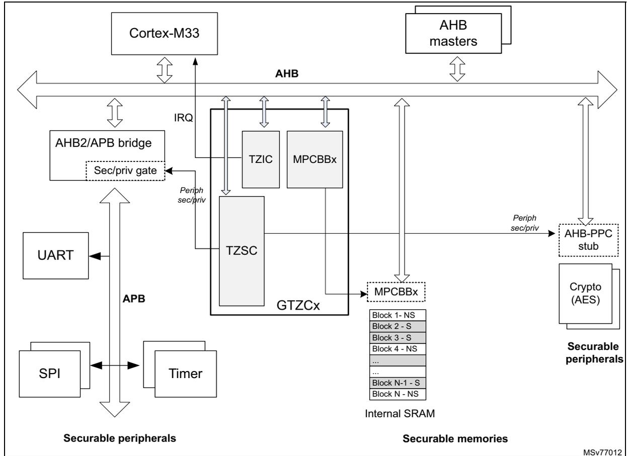
The diagram illustrates the GTZC subsystem within an Armv8-M architecture. At the top, the Cortex-M33 processor and AHB masters are connected to a common AHB bus. Below the AHB bus, an AHB2/APB bridge is present, containing a 'Sec/priv gate'. This bridge connects to the APB bus, which in turn connects to securable peripherals including UART, SPI, and a Timer. The GTZC (Global TrustZone Controller) is shown as a central block containing subblocks TZIC, MPCBBx, TZSC, and GTZCx. The Cortex-M33 is connected to the GTZC via an IRQ line. The GTZC is also connected to the AHB bus and to the APB bus via the AHB2/APB bridge. The GTZC controls the security state of peripherals and memories. A list of securable memories is shown, consisting of blocks 1 through N, alternating between Non-Secure (NS) and Secure (S) states: Block 1- NS, Block 2 - S, Block 3 - S, Block 4 - NS, ..., Block N-1 - S, Block N - NS. These memories are part of the Internal SRAM. Other securable peripherals, such as Crypto (AES), are connected to the AHB bus via an AHB-PPC stub. The diagram is labeled with 'Securable peripherals' and 'Securable memories' at the bottom. A reference code 'MSv77012' is visible in the bottom right corner.
5.0.3 GTZC implementation
The STM32U3 series devices embed one instance of GTZC.
Table 22. GTZC features
| GTZC subblocks | GTZC1 |
|---|---|
| TZSC | X |
| TZIC | X |
| MPCBB subblock on STM32U356/366 and STM32U375/385 | MPCBB1/2 |
| MPCBB subblock on STM32U3B5/3C5 | MPCBB1/2/3/4 |
The tables below show the address offset of GTZC subblocks versus GTZC base address (refer to Section 2.3.2 for GTZC1 base addresses).
Table 23. GTZC1 subblocks address offset for STM32U356/366 and STM32U375/385
| GTZC1 subblock | Address offset |
|---|---|
| GTZC1_TZSC | 0x0 |
| GTZC1_TZIC | 0x400 |
| GTZC1_MPCBB1 | 0x800 |
| GTZC1_MPCBB2 | 0xC00 |
Table 24. GTZC1 subblocks address offset for STM32U3B5/3C5
| GTZC1 subblock | Address offset |
|---|---|
| GTZC1_TZSC | 0x0 |
| GTZC1_TZIC | 0x400 |
| GTZC1_MPCBB1 | 0x800 |
| GTZC1_MPCBB2 | 0xC00 |
| GTZC1_MPCBB3 | 0x1000 |
| GTZC1_MPCBB4 | 0x1400 |
The tables below describe the characteristics of the available MPCBB.
Table 25. MPCBB resource assignment for STM32U356/366
| GTZC | MPC | Resource | Memory size (Kbytes) | Block size (bytes) | Number of blocks | Number of super-blocks |
|---|---|---|---|---|---|---|
| GTZC1 | MPCBB1 | SRAM1 | 128 | 512 | 256 | 8 |
| MPCBB2 | SRAM2 | 64 | 128 | 4 |
Table 26. MPCBB resource assignment for STM32U375/385
| GTZC | MPC | Resource | Memory size (Kbytes) | Block size (bytes) | Number of blocks | Number of super-blocks |
|---|---|---|---|---|---|---|
| GTZC1 | MPCBB1 | SRAM1 | 192 | 512 | 384 | 12 |
| MPCBB2 | SRAM2 | 64 | 128 | 4 |
Table 27. MPCBB resource assignment for STM32U3B5/3C5
| GTZC | MPC | Resource | Memory size (Kbytes) | Block size (bytes) | Number of blocks | Number of super-blocks |
|---|---|---|---|---|---|---|
| GTZC1 | MPCBB1 | SRAM1 | 192 | 512 | 384 | 12 |
| MPCBB2 | SRAM2 | 64 | 128 | 4 | ||
| MPCBB3 | SRAM3 | 320 | 640 | 20 | ||
| MPCBB4 | SRAM4 | 64 (1) | 160 (1) | 5 (1) |
- 1. The total SRAM4 addressing range is 80 Kbytes due BRAM-AB dual port address remapping. MPCBB4 covers the 80 kBytes including BRAM-AB.
5.1 GTZC functional description
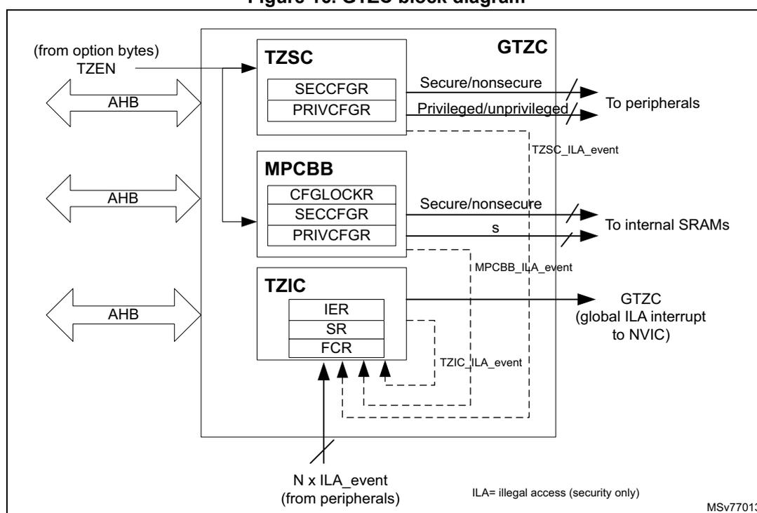
5.1.1 GTZC block diagram
Figure 16 describes the combined feature of TZSC, MPCBB and TZIC. Each subblock is controlled by its own AHB configuration port.
The TZSC defines which peripheral is secure and/or privileged. The privileged configuration bit of a peripheral can be modified by a secure privileged transaction when the peripheral is configured as secure. Otherwise, a privileged transaction (nonsecure) is sufficient.
On the opposite, the secure configuration bit of a peripheral can be modified only with a secure privileged transaction if the peripheral is configured as privileged. Otherwise, a secure transaction (unprivileged) is sufficient.
The secure configuration bit of a given ram block can be modified only with a secure privileged transaction if the same RAM block is configured as privileged. Otherwise, a secure transaction (unprivileged) is sufficient.
The TZIC gathers illegal events generated within the system when an illegal access is detected. TZIC can then generate a secure interrupt towards the CPU if needed.
Figure 16. GTZC block diagram
5.1.2 Illegal access definition
Three different types of illegal access exist:
- • Illegal nonsecure access
Any nonsecure transaction trying to write a secure resource is considered as illegal and thus the addressed resource generates an illegal access interrupt for illegal write access and a bus error for illegal fetch access. However some exceptions exist on secure and privileged configuration registers: these later ones authorize non secure read access to secure registers (see GTZC_TZSC_SECCFGRx and GTZC_TZSC_PRIVCFGRx).
- • Illegal secure access
Any secure transaction trying to access nonsecure block in internal block-based SRAM is considered as illegal.
Correct TZIC settings allows the capture of the associated event and then generates the GTZC_IRQn interrupt to the NVIC. This applies for read, write and execute access.
Concerning the MPCBB controller, there is an option to ignore secure data read/write access on nonsecure SRAM blocks, by setting the SRWILADIS bit in the GTZC_MPCBBz_CR register. Secure read and write data transactions are then allowed on nonsecure SRAM blocks, while secure execution access remains not allowed.
Any secure execute transaction trying to access a nonsecure peripheral register is considered as illegal and generate a bus error.
- • Illegal unprivileged access
Any unprivileged transaction trying to access a privileged resource is considered as illegal. There is no illegal access event generated for illegal read and write access. The
addressed resource follows a silent-fail behavior, returning all zero data for read and ignoring any write. No bus error is generated. A bus error is generated when any unprivileged execute transaction tries to access a privileged memory.
5.1.3 TrustZone security controller (TZSC)
The TZSC is composed of a configurable set of registers, providing the following features:
- • Control of secure and privileged state for all peripherals, done through:
- – GTZC_TZSC_SECCFGRx registers to control AHB/APB firewall stubs for the securable peripherals
- – GTZC_TZSC_PRIVCFG Rx registers to control AHB/APB firewall stubs for the privileged peripherals
5.1.4 Memory protection controller - block based (MPCBB)
The MPCBB is composed of a configurable set of registers allowing to define security and privileged policy for internal SRAM memories. The security and privileged policy can be individually configured per each 512-byte block of SRAM.
Figure 17. MPCBB block diagram
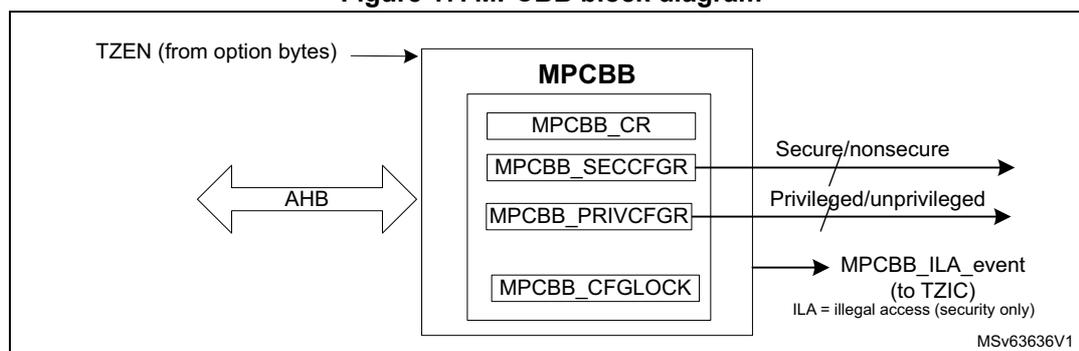
In order to setup the MPCBB, the following actions are needed (for example at boot time):
- • Secure firmware must define which memory blocks are secure by setting the correct bits in GTZC_MPCBBz_SECCFG Rx.
- • Privileged firmware must define which memory blocks are privileged by setting the correct bits in GTZC_MPCBBz_PRIVCFG Rx.
A MPCBB super-block is made of 32 consecutive blocks. For each super-block, secure application can lock all related security/privileged bits using the correct bits in GTZC_MPCBBz_CFGLOCKR1. This lock remains active until the next system reset.
Note: The block size is 512 bytes. The super-block size is \( 512 * 32 = 16 \) Kbytes.
5.1.5 TrustZone illegal access controller (TZIC)
The TZIC concentrates all illegal access source events. It is used only when the system is TrustZone enabled (TZEN = 1).
TZIC allows the trace (flag) of which event triggered the secure illegal access interrupt. Register masks (GTZC_TZIC_IERx) are available to filter unwanted event. On unmasked illegal event, TZIC generates the GTZC_IRQn interrupt to the NVIC.
For each illegal event source, a status flag and a clear bit exist (respectively within GTZC_TZIC_SRx and GTZC_TZIC_FCRx). The reset value of mask registers (GTZC_TZIC_IERx) is such that all events are masked.
5.1.6 Power-on/reset state
The power-on and reset state of the TZSC clear to 0 all bits of GTZC_TZSC_SECCFGRx and GTZC_TZSC_PRIVCFGRx, meaning that all securable peripherals are respectively set to nonsecure and unprivileged.
For internal SRAMx (x = 1 to 2 for STM32U356/366/375/385, x = 1 to 4 for STM32U3B5/3C5), all GTZC_MPCBBz_SECCFGRx and GTZC_MPCBBz_PRIVCFGRx are set:
- • to 0xFFFF FFFF, making these internal memories block secure and privileged by default when TrustZone security is enabled at system level (TZEN = 1).
- • to 0x0000 0000, making these internal memories block nonsecure and unprivileged by default when TrustZone security is disabled at system level (TZEN = 0).
Secure boot code can then program the security settings, making components secure or not as needed.
5.1.7 GTZC interrupts
TZIC is a secure peripheral, thus it systematically generates an illegal access event when accessed by a nonsecure access. The MPCBB and TZSC are TrustZone-aware peripherals, meaning that secure and nonsecure registers co-exist within the peripheral.
Table 28. GTZC interrupt request
| Interrupt acronym | Interrupt event | Event flag | Enable control bit | Interrupt clear method | Exit Sleep mode | Exit Stop mode | Exit Standby mode |
|---|---|---|---|---|---|---|---|
| GTZC | Illegal access | All flags in GTZC_TZIC_SRx | All bits in GTZC_TZIC_IERx | Write 1 in the bit GTZC_TZIC_FCRx | Yes | Yes | No |
5.2 GTZC1 TZSC registers
All registers are accessed only by words (32-bit).
5.2.1 GTZC1 TZSC control register (GTZC1_TZSC_CR)
Address offset: 0x000
Reset value: 0x0000 0000
Secure privileged access only.
| 31 | 30 | 29 | 28 | 27 | 26 | 25 | 24 | 23 | 22 | 21 | 20 | 19 | 18 | 17 | 16 |
| Res. | Res. | Res. | Res. | Res. | Res. | Res. | Res. | Res. | Res. | Res. | Res. | Res. | Res. | Res. | Res. |
| 15 | 14 | 13 | 12 | 11 | 10 | 9 | 8 | 7 | 6 | 5 | 4 | 3 | 2 | 1 | 0 |
| Res. | Res. | Res. | Res. | Res. | Res. | Res. | Res. | Res. | Res. | Res. | Res. | Res. | Res. | Res. | LCK |
| rs | |||||||||||||||
Bits 31:1 Reserved, must be kept at reset value.
Bit 0 LCK : Lock GTZC1_TZSC_SECCFGRx and GTZC1_TZSC_PRIVCFGRx configuration until next reset
This bit is cleared by default and once set, it cannot be reset until system reset.
0: Configuration of all GTZC1_TZSC_SECCFGRx and GTZC1_TZSC_PRIVCFGRx registers not locked
1: Configuration of all GTZC1_TZSC_SECCFGRx and GTZC1_TZSC_PRIVCFGRx registers locked
5.2.2 GTZC1 TZSC secure configuration register 1 (GTZC1_TZSC_SECCFGR1)
Address offset: 0x010
Reset value: 0x0000 0000
Write-secure access only.
This register can be written only by secure privileged transaction when corresponding GTZC1_TZSC_PRIVCFGR register bit is set to 1. If a given PRIV bit is not set, the equivalent SEC bit can be written by secure unprivileged transaction.
Read accesses are authorized for any type of transactions, secure or not, privileged or not.
| 31 | 30 | 29 | 28 | 27 | 26 | 25 | 24 | 23 | 22 | 21 | 20 | 19 | 18 | 17 | 16 |
|---|---|---|---|---|---|---|---|---|---|---|---|---|---|---|---|
| Res. | Res. | Res. | Res. | Res. | Res. | SPI4SEC | VREFBUSEC | OPAMPSEC | I3C1SEC | SPI3SEC | FDCAN2SEC | Res. | FDCAN1SEC | LPTIM2SEC | I2C4SEC |
| rw | rw | rw | rw | rw | rw | rw | rw | rw | |||||||
| 15 | 14 | 13 | 12 | 11 | 10 | 9 | 8 | 7 | 6 | 5 | 4 | 3 | 2 | 1 | 0 |
| CRSSEC | I2C2SEC | I2C1SEC | UART5SEC | UART4SEC | USART3SEC | USART2SEC | SPI12SEC | IWDGSEC | WWDGSEC | TIM7SEC | TIM6SEC | Res. | TIM4SEC | TIM3SEC | TIM2SEC |
| rw | rw | rw | rw | rw | rw | rw | rw | rw | rw | rw | rw | rw | rw | rw |
Bits 31:26 Reserved, must be kept at reset value.
Bit 25 SPI4SEC : Secure access mode for VREFBUF
0: Nonsecure
1: Secure
Note: This bit is only available on STM32U3B5/3C5.
Bit 24 VREFBUSEC : Secure access mode for VREFBUF
0: Nonsecure
1: Secure
Bit 23 OPAMPSEC : Secure access mode for OPAMP
0: Nonsecure
1: Secure
Bit 22 I3C1SEC : Secure access mode for I3C1
0: Nonsecure
1: Secure
Bit 21 SPI3SEC : Secure access mode for SPI3
0: Nonsecure
1: Secure
Bit 20 FDCAN2SEC : Secure access mode for FDCAN2
0: Nonsecure
1: Secure
Caution: The FDCAN SRAM is secure only when all FDCAN instances are configured as secure
Note: This bit is only available on STM32U3B5/3C5.
Bit 19 Reserved, must be kept at reset value.
Bit 18 FDCAN1SEC : Secure access mode for FDCAN1
0: Nonsecure
1: Secure
Caution: The FDCAN SRAM is secure only when all FDCAN instances are configured as secure
Note: This bit is only available on STM32U375/385 and STM32U3B5/3C5.
Bit 17 LPTIM2SEC : Secure access mode for LPTIM2
0: Nonsecure
1: Secure
Bit 16 I2C4SEC : Secure access mode for I2C4
0: Nonsecure
1: Secure
Note: This bit is only available on STM32U3B5/3C5.
Bit 15 CRSSEC : Secure access mode for CRS
0: Nonsecure
1: Secure
Bit 14 I2C2SEC : Secure access mode for I2C2
0: Nonsecure
1: Secure
Note: This bit is only available on STM32U375/385 and STM32U3B5/3C5.
Bit 13 I2C1SEC : Secure access mode for I2C1
0: Nonsecure
1: Secure
Bit 12 UART5SEC : Secure access mode for UART5
0: Nonsecure
1: Secure
Bit 11 UART4SEC : Secure access mode for UART4
0: Nonsecure
1: Secure
Bit 10 USART3SEC : Secure access mode for USART3
0: Nonsecure
1: Secure
Bit 9 USART2SEC : Secure access mode for USART2
0: Nonsecure
1: Secure
Note: This bit is only available on STM32U3B5/3C5.
Bit 8 SPI2SEC : Secure access mode for SPI2
0: Nonsecure
1: Secure
Bit 7 IWDGSEC : Secure access mode for IWDG
0: Nonsecure
1: Secure
Bit 6 WWDGSEC : Secure access mode for WWDG
0: Nonsecure
1: Secure
Bit 5 TIM7SEC : Secure access mode for TIM7
0: Nonsecure
1: Secure
Bit 4 TIM6SEC : Secure access mode for TIM6
0: Nonsecure
1: Secure
Bit 3 Reserved, must be kept at reset value.
Bit 2 TIM4SEC : Secure access mode for TIM4
0: Nonsecure
1: Secure
Bit 1 TIM3SEC : Secure access mode for TIM3
0: Nonsecure
1: Secure
Bit 0 TIM2SEC : Secure access mode for TIM2
0: Nonsecure
1: Secure
5.2.3 GTZC1 TZSC secure configuration register 2 (GTZC1_TZSC_SECCFGR2)
Address offset: 0x014
Reset value: 0x0000 0000
Write-secure access only.
This register can be written only by secure privileged transaction when corresponding GTZC1_TZSC_PRIVCFGR register bit is set to 1. If a given PRIV is not set, the equivalent SEC bit can be written by secure unprivileged transaction.
Read accesses are authorized for any type of transactions, secure or not, privileged or not.
| 31 | 30 | 29 | 28 | 27 | 26 | 25 | 24 | 23 | 22 | 21 | 20 | 19 | 18 | 17 | 16 |
|---|---|---|---|---|---|---|---|---|---|---|---|---|---|---|---|
| Res. | Res. | Res. | Res. | Res. | Res. | Res. | Res. | Res. | Res. | Res. | Res. | Res. | Res. | LCDSEC | COMPSEC |
| 15 | 14 | 13 | 12 | 11 | 10 | 9 | 8 | 7 | 6 | 5 | 4 | 3 | 2 | 1 | 0 |
| LPTIM4SEC | LPTIM3SEC | LPTIM1SEC | I2C3SEC | LPUART1SEC | I3C2SEC | USBSEC | TIM12SEC | SAI1SEC | TIM17SEC | TIM16SEC | TIM15SEC | USART1SEC | TIM8SEC | SPI1SEC | TIM1SEC |
| rw | rw | rw | rw | rw | rw | rw | rw | rw | rw | rw | rw | rw | rw | rw | rw |
Bits 31:18 Reserved, must be kept at reset value.
Bit 17 LCDSEC : Secure access mode for LCD
0: Nonsecure
1: Secure
Note: This bit is only available on STM32U356/366.
Bit 16 COMPSEC : Secure access mode for COMP
0: Nonsecure
1: Secure
Bit 15 LPTIM4SEC : Secure access mode for LPTIM4
0: Nonsecure
1: Secure
Bit 14 LPTIM3SEC : Secure access mode for LPTIM3
0: Nonsecure
1: Secure
Bit 13 LPTIM1SEC : Secure access mode for LPTIM1
0: Nonsecure
1: Secure
Bit 12 I2C3SEC : Secure access mode for I2C3
0: Nonsecure
1: Secure
Bit 11 LPUART1SEC : Secure access mode for LPUART1
0: Nonsecure
1: Secure
Bit 10 I3C2SEC : Secure access mode for I3C2
0: Nonsecure
1: Secure
Note: This bit is only available on STM32U375/385 and STM32U3B5/3C5.
Bit 9 USBSEC : Secure access mode for USB
0: Nonsecure
1: Secure
Bit 8 TIM12SEC : Secure access mode for TIM12
0: Nonsecure
1: Secure
Note: This bit is only available on STM32U3B5/3C5.
Bit 7 SAI1SEC : Secure access mode for SAI1
0: Nonsecure
1: Secure
Note: This bit is only available on STM32U375/385 and STM32U3B5/3C5.
Bit 6 TIM17SEC : Secure access mode for TIM17
0: Nonsecure
1: Secure
Bit 5 TIM16SEC : Secure access mode for TIM16
0: Nonsecure
1: Secure
Bit 4 TIM15SEC : Secure access mode for TIM15
0: Nonsecure
1: Secure
Bit 3 USART1SEC : Secure access mode for USART1
0: Nonsecure
1: Secure
Bit 2 TIM8SEC : Secure access mode for TIM8
0: Nonsecure
1: Secure
Note: This bit is only available on STM32U3B5/3C5.
Bit 1 SPI1SEC : Secure access mode for SPI1
0: Nonsecure
1: Secure
Bit 0 TIM1SEC : Secure access mode for TIM1
0: Nonsecure
1: Secure
5.2.4 GTZC1 TZSC secure configuration register 3 (GTZC1_TZSC_SECCFGR3)
Address offset: 0x018
Reset value: 0x0000 0000
Write-secure access only.
This register can be written only by secure privileged transaction when corresponding GTZC1_TZSC_PRIVCFGR register bit is set to 1. If a given PRIV is not set, the equivalent SEC bit can be written by secure unprivileged transaction.
Read accesses are authorized for any type of transactions, secure or not, privileged or not.
| 31 | 30 | 29 | 28 | 27 | 26 | 25 | 24 | 23 | 22 | 21 | 20 | 19 | 18 | 17 | 16 |
|---|---|---|---|---|---|---|---|---|---|---|---|---|---|---|---|
| Res. | Res. | HSP1SEC | Res. | Res. | Res. | Res. | ADF1SEC | DAC1SEC | RAMCFGSEC | Res. | OCTOSPI1_REGSEC | Res. | Res. | SDMMC1SEC | CCBSEC |
| rw | rw | rw | rw | rw | rw | rw | |||||||||
| 15 | 14 | 13 | 12 | 11 | 10 | 9 | 8 | 7 | 6 | 5 | 4 | 3 | 2 | 1 | 0 |
| SAESSSEC | PKASEC | RNGSEC | HASHSEC | AESSSEC | Res. | Res. | ADC12SEC | Res. | ICACHE_REGSEC | Res. | TSCSEC | CRCSEC | Res. | Res. | Res. |
| rw | rw | rw | rw | rw | rw | rw | rw | rw |
Bits 31:30 Reserved, must be kept at reset value.
Bit 29 HSP1SEC : Secure access mode for HSP1
0: Nonsecure
1: Secure
Note: This bit is only available on STM32U3B5/3C5.
Bits 28:25 Reserved, must be kept at reset value.
Bit 24 ADF1SEC : Secure access mode for ADF1
0: Nonsecure
1: Secure
Note: This bit is only available on STM32U375/385 and STM32U3B5/3C5.
Bit 23 DAC1SEC : Secure access mode for DAC1
0: Nonsecure
1: Secure
Bit 22 RAMCFGSEC : Secure access mode for RAMCFG
0: Nonsecure
1: Secure
Bit 21 Reserved, must be kept at reset value.
Bit 20 OCTOSPI1_REGSEC : Secure access mode for OCTOSPI1 registers
0: Nonsecure
1: Secure
Bits 19:18 Reserved, must be kept at reset value.
- Bit 17
SDMMC1SEC
: Secure access mode for SDMMC1
0: Nonsecure
1: Secure
Note: This bit is only available on STM32U375/385 and STM32U3B5/3C5. - Bit 16
CCBSEC
: Secure access mode for CCB
0: Nonsecure
1: Secure - Bit 15
SAESSEC
: Secure access mode for SAES
0: Nonsecure
1: Secure - Bit 14
PKASEC
: Secure access mode for PKA
0: Nonsecure
1: Secure - Bit 13
RNGSEC
: Secure access mode for RNG
0: Nonsecure
1: Secure - Bit 12
HASHSEC
: Secure access mode for HASH
0: Nonsecure
1: Secure - Bit 11
AESSEC
: Secure access mode for AES
0: Nonsecure
1: Secure - Bits 10:9 Reserved, must be kept at reset value.
- Bit 8
ADC12SEC
: Secure access mode for ADC1 and ADC2
0: Nonsecure
1: Secure - Bit 7 Reserved, must be kept at reset value.
- Bit 6
ICACHE_REGSEC
: Secure access mode for ICACHE registers
0: Nonsecure
1: Secure - Bit 5 Reserved, must be kept at reset value.
- Bit 4
TSCSEC
: Secure access mode for TSC
0: Nonsecure
1: Secure - Bit 3
CRCSEC
: Secure access mode for CRC
0: Nonsecure
1: Secure - Bits 2:0 Reserved, must be kept at reset value.
5.2.5 GTZC1 TZSC privilege configuration register 1 (GTZC1_TZSC_PRIVCFGR1)
Address offset: 0x020
Reset value: 0x0000 0000
Write-privileged access only.
This register can be read or written only by secure privileged transaction when corresponding GTZC1_TZSC_SECCFGR register bit is set to 1. If a given SEC bit is not set, the equivalent PRIV bit can be read/written by nonsecure privileged transaction.
Read accesses are authorized for any type of transactions, secure or not, privileged or not.
| 31 | 30 | 29 | 28 | 27 | 26 | 25 | 24 | 23 | 22 | 21 | 20 | 19 | 18 | 17 | 16 |
|---|---|---|---|---|---|---|---|---|---|---|---|---|---|---|---|
| Res. | Res. | Res. | Res. | Res. | Res. | SPI4P RIV | VREFB UFPRI V | OPAMP PRIV | I3C1PR IV | SPI3P RIV | FDCAN 2PRIV | Res. | FDCAN 1PRIV | LPTIM2 PRIV | I2C4PR IV |
| rw | rw | rw | rw | rw | rw | rw | rw | rw | |||||||
| 15 | 14 | 13 | 12 | 11 | 10 | 9 | 8 | 7 | 6 | 5 | 4 | 3 | 2 | 1 | 0 |
| CRSPR IV | I2C2PR IV | I2C1PR IV | UART5 PRIV | UART4 PRIV | USART 3PRIV | USART 2PRIV | SPI2P RIV | IWDGP RIV | WWDG PRIV | TIM7P RIV | TIM6P RIV | Res. | TIM4P RIV | TIM3P RIV | TIM2P RIV |
| rw | rw | rw | rw | rw | rw | rw | rw | rw | rw | rw | rw | rw | rw | rw |
Bits 31:26 Reserved, must be kept at reset value.
Bit 25 SPI4PRIV : Privileged access mode for SPI4
0: Unprivileged
1: Privileged
Note: This bit is only available on STM32U3B5/3C5.
Bit 24 VREFBUFPRIV : Privileged access mode for VREFBUF
0: Unprivileged
1: Privileged
Bit 23 OPAMPPRIV : Privileged access mode for OPAMP
0: Unprivileged
1: Privileged
Bit 22 I3C1PRIV : Privileged access mode for I3C1
0: Unprivileged
1: Privileged
Bit 21 SPI3PRIV : Privileged access mode for SPI3
0: Unprivileged
1: Privileged
Bit 20 FDCAN2PRIV : Privileged access mode for FDCAN2
0: Unprivileged
1: Privileged
Caution: The FDCAN SRAM is privileged only when all FDCAN instances are configured as privileged
Note: This bit is only available on STM32U3B5/3C5.
Bit 19 Reserved, must be kept at reset value.
Bit 18 FDCAN1PRIV : Privileged access mode for FDCAN1
0: Unprivileged
1: Privileged
Caution: The FDCAN SRAM is privileged only when all FDCAN instances are configured as privileged
Note: This bit is only available on STM32U375/385 and STM32U3B5/3C5.
Bit 17 LPTIM2PRIV : Privileged access mode for LPTIM2
0: Unprivileged
1: Privileged
Bit 16 I2C4PRIV : Privileged access mode for I2C4
0: Unprivileged
1: Privileged
Note: This bit is only available on STM32U3B5/3C5.
Bit 15 CRSPRIV : Privileged access mode for CRS
0: Unprivileged
1: Privileged
Bit 14 I2C2PRIV : Privileged access mode for I2C2
0: Unprivileged
1: Privileged
Note: This bit is only available on STM32U375/385 and STM32U3B5/3C5.
Bit 13 I2C1PRIV : Privileged access mode for I2C1
0: Unprivileged
1: Privileged
Bit 12 UART5PRIV : Privileged access mode for UART5
0: Unprivileged
1: Privileged
Bit 11 UART4PRIV : Privileged access mode for UART4
0: Unprivileged
1: Privileged
Bit 10 USART3PRIV : Privileged access mode for USART3
0: Unprivileged
1: Privileged
Bit 9 USART2PRIV : Privileged access mode for USART2
0: Unprivileged
1: Privileged
Note: This bit is only available on STM32U3B5/3C5.
Bit 8 SPI2PRIV : Privileged access mode for SPI2
0: Unprivileged
1: Privileged
Bit 7 IWDGPRIV : Privileged access mode for IWDG
0: Unprivileged
1: Privileged
Bit 6 WWDGPRIV : Privileged access mode for WWDG
0: Unprivileged
1: Privileged
- Bit 5
TIM7PRIV
: Privileged access mode for TIM7
0: Unprivileged
1: Privileged - Bit 4
TIM6PRIV
: Privileged access mode for TIM6
0: Unprivileged
1: Privileged - Bit 3 Reserved, must be kept at reset value.
- Bit 2
TIM4PRIV
: Privileged access mode for TIM4
0: Unprivileged
1: Privileged - Bit 1
TIM3PRIV
: Privileged access mode for TIM3
0: Unprivileged
1: Privileged - Bit 0
TIM2PRIV
: Privileged access mode for TIM2
0: Unprivileged
1: Privileged
5.2.6 GTZC1 TZSC privilege configuration register 2 (GTZC1_TZSC_PRIVCFGR2)
Address offset: 0x024
Reset value: 0x0000 0000
Write-privileged access only.
This register can be read or written only by secure privileged transaction when corresponding GTZC1_TZSC_SECCFGR register bit is set to 1. If a given SEC bit is not set, the equivalent PRIV bit can be read/written by nonsecure privileged transaction.
Read accesses are authorized for any type of transactions, secure or not, privileged or not.
| 31 | 30 | 29 | 28 | 27 | 26 | 25 | 24 | 23 | 22 | 21 | 20 | 19 | 18 | 17 | 16 |
|---|---|---|---|---|---|---|---|---|---|---|---|---|---|---|---|
| Res. | Res. | Res. | Res. | Res. | Res. | Res. | Res. | Res. | Res. | Res. | Res. | Res. | Res. | LCDPRIV | COMP PRIV |
| rw | rw | ||||||||||||||
| 15 | 14 | 13 | 12 | 11 | 10 | 9 | 8 | 7 | 6 | 5 | 4 | 3 | 2 | 1 | 0 |
| LPTIM4 PRIV | LPTIM3 PRIV | LPTIM1 PRIV | I2C3PRIV | LPUART1 PRIV | I3C2PRIV | USBPRIV | TIM12PRIV | SAI1PRIV | TIM17PRIV | TIM16PRIV | TIM15PRIV | USART1PRIV | TIM8PRIV | SPI1PRIV | TIM1PRIV |
| rw | rw | rw | rw | rw | rw | rw | rw | rw | rw | rw | rw | rw | rw | rw | rw |
Bits 31:18 Reserved, must be kept at reset value.
- Bit 17
LCDPRIV
: Privileged access mode for LCD
0: Unprivileged
1: Privileged
Note: This bit is only available on STM32U356/366.
- Bit 16
COMPPRIV
: Privileged access mode for COMP
0: Unprivileged
1: Privileged
Bit 15 LPTIM4PRIV : Privileged access mode for LPTIM4
0: Unprivileged
1: Privileged
Bit 14 LPTIM3PRIV : Privileged access mode for LPTIM3
0: Unprivileged
1: Privileged
Bit 13 LPTIM1PRIV : Privileged access mode for LPTIM1
0: Unprivileged
1: Privileged
Bit 12 I2C3PRIV : Privileged access mode for I2C3
0: Unprivileged
1: Privileged
Bit 11 LPUART1PRIV : Privileged access mode for LPUART1
0: Unprivileged
1: Privileged
Bit 10 I3C2PRIV : Privileged access mode for I3C2
0: Unprivileged
1: Privileged
Note: This bit is only available on STM32U375/385 and STM32U3B5/3C5.
Bit 9 USBPRIV : Privileged access mode for USB
0: Unprivileged
1: Privileged
Bit 8 TIM12PRIV : Privileged access mode for TIM12
0: Unprivileged
1: Privileged
Note: This bit is only available on STM32U3B5/3C5.
Bit 7 SAI1PRIV : Privileged access mode for SAI1
0: Unprivileged
1: Privileged
Note: This bit is only available on STM32U375/385 and STM32U3B5/3C5.
Bit 6 TIM17PRIV : Privileged access mode for TIM17
0: Unprivileged
1: Privileged
Bit 5 TIM16PRIV : Privileged access mode for TIM16
0: Unprivileged
1: Privileged
Bit 4 TIM15PRIV : Privileged access mode for TIM15
0: Unprivileged
1: Privileged
Bit 3 USART1PRIV : Privileged access mode for USART1
0: Unprivileged
1: Privileged
Bit 2 TIM8PRIV : Privileged access mode for TIM8
0: Unprivileged
1: Privileged
Note: This bit is only available on STM32U3B5/3C5.
Bit 1 SPI1PRIV : Privileged access mode for SPI1
0: Unprivileged
1: Privileged
Bit 0 TIM1PRIV : Privileged access mode for TIM1
0: Unprivileged
1: Privileged
5.2.7 GTZC1 TZSC privilege configuration register 3 (GTZC1_TZSC_PRIVCFGR3)
Address offset: 0x0028
Reset value: 0x0000 0000
Write-privileged access only.
This register can be read or written only by secure privileged transaction when corresponding GTZC1_TZSC_SECCFGR register bit is set to 1. If a given SEC bit is not set, the equivalent PRIV bit can be read/written by nonsecure privileged transaction.
Read accesses are authorized for any type of transactions, secure or not, privileged or not.
| 31 | 30 | 29 | 28 | 27 | 26 | 25 | 24 | 23 | 22 | 21 | 20 | 19 | 18 | 17 | 16 |
|---|---|---|---|---|---|---|---|---|---|---|---|---|---|---|---|
| Res. | Res. | HSP1P RIV | Res. | Res. | Res. | Res. | ADF1P RIV | DAC1P RIV | RAMC FGPRI V | Res. | OCTOS PI1_RE GPRIV | Res. | Res. | SDMM C1PRI V | CCBPR IV |
| rw | rw | rw | rw | rw | rw | rw | |||||||||
| 15 | 14 | 13 | 12 | 11 | 10 | 9 | 8 | 7 | 6 | 5 | 4 | 3 | 2 | 1 | 0 |
| SAESP RIV | PKAPR IV | RNGP RIV | HASHP RIV | AESPR IV | Res. | Res. | ADC12 PRIV | Res. | ICACH E_REG PRIV | Res. | TSCPR IV | CRCP RIV | Res. | Res. | Res. |
| rw | rw | rw | rw | rw | rw | rw | rw | rw |
Bits 31:30 Reserved, must be kept at reset value.
Bit 29 HSP1PRIV : Privileged access mode for HSP1
0: Unprivileged
1: Privileged
Note: This bit is only available on STM32U3B5/3C5.
Bits 28:25 Reserved, must be kept at reset value.
Bit 24 ADF1PRIV : Privileged access mode for ADF1
0: Unprivileged
1: Privileged
Note: This bit is only available on STM32U375/385 and STM32U3B5/3C5.
Bit 23 DAC1PRIV : Privileged access mode for DAC1
0: Unprivileged
1: Privileged
- Bit 22
RAMCFGPRIV
: Privileged access mode for RAMCFG
0: Unprivileged
1: Privileged - Bit 21 Reserved, must be kept at reset value.
- Bit 20
OCTOSPI1_REGPRIV
: Privileged access mode for OCTOSPI1 registers
0: Unprivileged
1: Privileged - Bits 19:18 Reserved, must be kept at reset value.
- Bit 17
SDMMC1PRIV
: Privileged access mode for SDMMC1
0: Unprivileged
1: Privileged
Note: This bit is only available on STM32U375/385 and STM32U3B5/3C5. - Bit 16
CCBPRIV
: Privileged access mode for CCB
0: Unprivileged
1: Privileged - Bit 15
SAESPRIV
: Privileged access mode for SAES
0: Unprivileged
1: Privileged - Bit 14
PKAPRIV
: Privileged access mode for PKA
0: Unprivileged
1: Privileged - Bit 13
RNGPRIV
: Privileged access mode for RNG
0: Unprivileged
1: Privileged - Bit 12
HASHPRIV
: Privileged access mode for HASH
0: Unprivileged
1: Privileged - Bit 11
AESPRIV
: Privileged access mode for AES
0: Unprivileged
1: Privileged - Bits 10:9 Reserved, must be kept at reset value.
- Bit 8
ADC12PRIV
: Privileged access mode for ADC1 and ADC2
0: Unprivileged
1: Privileged - Bit 7 Reserved, must be kept at reset value.
- Bit 6
ICACHE_REGPRIV
: Privileged access mode for ICACHE registers
0: Unprivileged
1: Privileged - Bit 5 Reserved, must be kept at reset value.
- Bit 4
TSCPRIV
: Privileged access mode for TSC
0: Unprivileged
1: Privileged
Bit 3 CRCPRIV : Privileged access mode for CRC
0: Unprivileged
1: Privileged
Bits 2:0 Reserved, must be kept at reset value.
5.2.8 GTZC1 TZSC register map
Table 29. GTZC1 TZSC register map and reset values
| Offset | Register name | 31 | 30 | 29 | 28 | 27 | 26 | 25 | 24 | 23 | 22 | 21 | 20 | 19 | 18 | 17 | 16 | 15 | 14 | 13 | 12 | 11 | 10 | 9 | 8 | 7 | 6 | 5 | 4 | 3 | 2 | 1 | 0 |
|---|---|---|---|---|---|---|---|---|---|---|---|---|---|---|---|---|---|---|---|---|---|---|---|---|---|---|---|---|---|---|---|---|---|
| 0x000 | GTZC1_TZSC_CR | Res | Res | Res | Res | Res | Res | Res | Res | Res | Res | Res | Res | Res | Res | Res | Res | Res | Res | Res | Res | Res | Res | Res | Res | Res | Res | Res | Res | Res | Res | LCK | |
| Reset value | 0 | ||||||||||||||||||||||||||||||||
| 0x004-0x00C | Reserved | Reserved | |||||||||||||||||||||||||||||||
| 0x010 | GTZC1_TZSC_SEC_CFGR1 | Res | Res | Res | Res | Res | Res | SP4SEC | VREFBUFSEC | OPAMPSEC | I3C1SEC | SPI3SEC | FDCAN2SEC | Res | FDCAN1SEC | LPTIM2SEC | I2C4SEC | CRSSEC | I2C2SEC | I2C1SEC | UART5SEC | UART4SEC | USART3SEC | USART2SEC | SPI2SEC | IWDGSEC | WWDGSEC | TIM7SEC | TIM6SEC | Res | TIM4SEC | TIM3SEC | |
| Reset value | 0 | 0 | 0 | 0 | 0 | 0 | 0 | 0 | 0 | 0 | 0 | 0 | 0 | 0 | 0 | 0 | 0 | 0 | 0 | 0 | 0 | 0 | 0 | 0 | |||||||||
| 0x014 | GTZC1_TZSC_SEC_CFGR2 | Res | Res | Res | Res | Res | Res | Res | Res | Res | Res | Res | Res | Res | LCDSEC | COMPSEC | LPTIM4SEC | CRSSEC | LPTIM3SEC | LPTIM1SEC | I2C3SEC | LPUART1SEC | I3C2SEC | USBSEC | TIM12SEC | SAI1SEC | TIM17SEC | TIM16SEC | TIM15SEC | USART1SEC | TIM8SEC | SP11SEC | |
| Reset value | 0 | 0 | 0 | 0 | 0 | 0 | 0 | 0 | 0 | 0 | 0 | 0 | 0 | 0 | 0 | 0 | 0 | 0 | |||||||||||||||
| 0x018 | GTZC1_TZSC_SEC_CFGR3 | Res | Res | HSP1SEC | Res | Res | Res | Res | ADF1SEC | DAC1SEC | RAMCFGSEC | Res | OCTOSP11_REGSEC | Res | SDMMC1SEC | CCBSEC | SAESSEC | PKASEC | RNGSEC | HASHSEC | AESSEC | Res | Res | Res | ADC12SEC | Res | ICACHE_REGSEC | Res | TSCSEC | CRCSEC | Res | Res | Res |
| Reset value | 0 | 0 | 0 | 0 | 0 | 0 | 0 | 0 | 0 | 0 | 0 | 0 | 0 | 0 | 0 | 0 | |||||||||||||||||
| 0x01C | Reserved | Reserved | |||||||||||||||||||||||||||||||
| 0x020 | GTZC1_TZSC_PRI_VCFG1 | Res | Res | Res | Res | Res | Res | SP4PRIV | VREFBUFPV | OPAMPPRIV | I3C1PRIV | SPI3PRIV | FDCAN2PRIV | Res | FDCAN1PRIV | LPTIM2PRIV | I2C4PRIV | CRSPRIV | I2C2PRIV | I2C1PRIV | UART5PRIV | UART4PRIV | USART3PRIV | USART2PRIV | SPI2PRIV | IWDGPRIV | WWDGPRIV | TIM7PRIV | TIM6PRIV | Res | TIM4PRIV | TIM3PRIV | |
| Reset value | 0 | 0 | 0 | 0 | 0 | 0 | 0 | 0 | 0 | 0 | 0 | 0 | 0 | 0 | 0 | 0 | 0 | 0 | 0 | 0 | 0 | 0 | 0 | 0 | |||||||||
| 0x024 | GTZC1_TZSC_PRI_VCFG2 | Res | Res | Res | Res | Res | Res | Res | Res | Res | Res | Res | Res | Res | LCDPRIV | COMPPRIV | LPTIM4PRIV | CRSPRIV | LPTIM3PRIV | LPTIM1PRIV | I2C3PRIV | LPUART1PRIV | I3C2PRIV | USBPRIV | TIM12PRIV | SAI1PRIV | TIM17PRIV | TIM16PRIV | TIM15PRIV | USART1PRIV | TIM8PRIV | SP11PRIV | |
| Reset value | 0 | 0 | 0 | 0 | 0 | 0 | 0 | 0 | 0 | 0 | 0 | 0 | 0 | 0 | 0 | 0 | 0 | 0 | |||||||||||||||
| 0x028 | GTZC1_TZSC_PRI_VCFG3 | Res | Res | HSP1PRIV | Res | Res | Res | Res | ADF1PRIV | DAC1PRIV | RAMCFGPRIV | Res | OCTOSP11_REGPRIV | Res | SDMMC1PRIV | CCBPRIV | SAESPRIV | PKAPRIV | RNGPRIV | HASHPRIV | AESPRIV | Res | Res | Res | ADC12PRIV | Res | ICACHE_REGPRIV | Res | TSCPRIV | CRCPRIV | Res | Res | Res |
| Reset value | 0 | 0 | 0 | 0 | 0 | 0 | 0 | 0 | 0 | 0 | 0 | 0 | 0 | 0 | 0 | 0 | |||||||||||||||||
| 0x02C-0x03C | Reserved | Reserved | |||||||||||||||||||||||||||||||
Refer to Section 5.0.3: GTZC implementation .
5.3 GTZC1 TZIC registers
All registers are accessed only by words (32-bit).
5.3.1 GTZC1 TZIC interrupt enable register 1 (GTZC1_TZIC_IER1)
Address offset: 0x000
Reset value: 0x0000 0000
Secure privileged access only. This register is used to enable interrupt of illegal access.
| 31 | 30 | 29 | 28 | 27 | 26 | 25 | 24 | 23 | 22 | 21 | 20 | 19 | 18 | 17 | 16 |
|---|---|---|---|---|---|---|---|---|---|---|---|---|---|---|---|
| Res. | Res. | Res. | Res. | Res. | Res. | SPI4IE | VREFBU FIE | OPAMP IE | I3C1IE | SPI3IE | FDCAN 2IE | Res. | FDCAN 1IE | LPTIM2 IE | I2C4IE |
| rw | rw | rw | rw | rw | rw | rw | rw | rw | |||||||
| 15 | 14 | 13 | 12 | 11 | 10 | 9 | 8 | 7 | 6 | 5 | 4 | 3 | 2 | 1 | 0 |
| CRSIE | I2C2IE | I2C1IE | UART5I E | UART4I E | USART 3IE | USART 2IE | SPI2IE | IWDGI E | WWDG IE | TIM7IE | TIM6IE | Res. | TIM4IE | TIM3IE | TIM2IE |
| rw | rw | rw | rw | rw | rw | rw | rw | rw | rw | rw | rw | rw | rw | rw |
Bits 31:26 Reserved, must be kept at reset value.
Bit 25 SPI4IE : Illegal access interrupt enable for SPI4
0: Interrupt disabled
1: Interrupt enabled
Note: This bit is only available on STM32U3B5/3C5.
Bit 24 VREFBUFIE : Illegal access interrupt enable for VREFBUF
0: Interrupt disabled
1: Interrupt enabled
Bit 23 OPAMPIE : Illegal access interrupt enable for OPAMP
0: Interrupt disabled
1: Interrupt enabled
Bit 22 I3C1IE : Illegal access interrupt enable for I3C1
0: Interrupt disabled
1: Interrupt enabled
Bit 21 SPI3IE : Illegal access interrupt enable for SPI3
0: Interrupt disabled
1: Interrupt enabled
Bit 20 FDCAN2IE : Illegal access interrupt enable for FDCAN2
0: Interrupt disabled
1: Interrupt enabled
Note: This bit is only available on STM32U3B5/3C5.
Bit 19 Reserved, must be kept at reset value.
Bit 18 FDCAN1IE : Illegal access interrupt enable for FDCAN1 and FDCAN SRAM
0: Interrupt disabled
1: Interrupt enabled
Note: This bit is only available on STM32U375/385 and STM32U3B5/3C5.
Bit 17 LPTIM2IE : Illegal access interrupt enable for LPTIM2
0: Interrupt disabled
1: Interrupt enabled
Bit 16 I2C4IE : Illegal access interrupt enable for I2C4
0: Interrupt disabled
1: Interrupt enabled
Note: This bit is only available on STM32U3B5/3C5.
Bit 15 CRSIE : Illegal access interrupt enable for CRS
0: Interrupt disabled
1: Interrupt enabled
Bit 14 I2C2IE : Illegal access interrupt enable for I2C2
0: Interrupt disabled
1: Interrupt enabled
Note: This bit is only available on STM32U375/385 and STM32U3B5/3C5.
Bit 13 I2C1IE : Illegal access interrupt enable for I2C1
0: Interrupt disabled
1: Interrupt enabled
Bit 12 UART5IE : Illegal access interrupt enable for UART5
0: Interrupt disabled
1: Interrupt enabled
Bit 11 UART4IE : Illegal access interrupt enable for UART4
0: Interrupt disabled
1: Interrupt enabled
Bit 10 USART3IE : Illegal access interrupt enable for USART3
0: Interrupt disabled
1: Interrupt enabled
Bit 9 USART2IE : Illegal access interrupt enable for USART2
0: Interrupt disabled
1: Interrupt enabled
Note: This bit is only available on STM32U3B5/3C5.
Bit 8 SPI2IE : Illegal access interrupt enable for SPI2
0: Interrupt disabled
1: Interrupt enabled
Bit 7 IWDGIE : Illegal access interrupt enable for IWDG
0: Interrupt disabled
1: Interrupt enabled
Bit 6 WWDGIE : Illegal access interrupt enable for WWDG
0: Interrupt disabled
1: Interrupt enabled
Bit 5 TIM7IE : Illegal access interrupt enable for TIM7
0: Interrupt disabled
1: Interrupt enabled
Bit 4 TIM6IE : Illegal access interrupt enable for TIM6
0: Interrupt disabled
1: Interrupt enabled
Bit 3 Reserved, must be kept at reset value.
Bit 2 TIM4IE : Illegal access interrupt enable for TIM4
0: Interrupt disabled
1: Interrupt enabled
Bit 1 TIM3IE : Illegal access interrupt enable for TIM3
0: Interrupt disabled
1: Interrupt enabled
Bit 0 TIM2IE : Illegal access interrupt enable for TIM2
0: Interrupt disabled
1: Interrupt enabled
5.3.2 GTZC1 TZIC interrupt enable register 2 (GTZC1_TZIC_IER2)
Address offset: 0x004
Reset value: 0x0000 0000
Secure privileged access only. This register is used to enable interrupt of illegal access.
| 31 | 30 | 29 | 28 | 27 | 26 | 25 | 24 | 23 | 22 | 21 | 20 | 19 | 18 | 17 | 16 |
|---|---|---|---|---|---|---|---|---|---|---|---|---|---|---|---|
| Res. | Res. | Res. | Res. | Res. | Res. | Res. | Res. | Res. | Res. | Res. | Res. | Res. | Res. | LCDIE | COMPIE |
| rw | rw | ||||||||||||||
| 15 | 14 | 13 | 12 | 11 | 10 | 9 | 8 | 7 | 6 | 5 | 4 | 3 | 2 | 1 | 0 |
| LPTIM4IE | LPTIM3IE | LPTIM1IE | I2C3IE | LPUART1IE | I3C2IE | USBIE | TIM12IE | SAI1IE | TIM17IE | TIM16IE | TIM15IE | USART1IE | TIM8IE | SPI1IE | TIM1IE |
| rw | rw | rw | rw | rw | rw | rw | rw | rw | rw | rw | rw | rw | rw | rw | rw |
Bits 31:18 Reserved, must be kept at reset value.
Bit 17 LCDIE : Illegal access interrupt enable for LCD
0: Interrupt disabled
1: Interrupt enabled
Note: This bit is only available on STM32U356/366.
Bit 16 COMPIE : Illegal access interrupt enable for COMP
0: Interrupt disabled
1: Interrupt enabled
Bit 15 LPTIM4IE : Illegal access interrupt enable for LPTIM4
0: Interrupt disabled
1: Interrupt enabled
Bit 14 LPTIM3IE : Illegal access interrupt enable for LPTIM3
0: Interrupt disabled
1: Interrupt enabled
Bit 13 LPTIM1IE : Illegal access interrupt enable for LPTIM1
0: Interrupt disabled
1: Interrupt enabled
Bit 12 I2C3IE : Illegal access interrupt enable for I2C3
0: Interrupt disabled
1: Interrupt enabled
Bit 11 LPUART1IE : Illegal access interrupt enable for LPUART1
0: Interrupt disabled
1: Interrupt enabled
Bit 10 I3C2IE : Illegal access interrupt enable for I3C2
0: Interrupt disabled
1: Interrupt enabled
Note: This bit is only available on STM32U375/385 and STM32U3B5/3C5.
Bit 9 USBIE : Illegal access interrupt enable for USB
0: Interrupt disabled
1: Interrupt enabled
Bit 8 TIM12IE : Illegal access interrupt enable for TIM12
0: Interrupt disabled
1: Interrupt enabled
Note: This bit is only available on STM32U3B5/3C5.
Bit 7 SAI1IE : Illegal access interrupt enable for SAI1
0: Interrupt disabled
1: Interrupt enabled
Note: This bit is only available on STM32U375/385 and STM32U3B5/3C5.
Bit 6 TIM17IE : Illegal access interrupt enable for TIM17
0: Interrupt disabled
1: Interrupt enabled
Bit 5 TIM16IE : Illegal access interrupt enable for TIM16
0: Interrupt disabled
1: Interrupt enabled
Bit 4 TIM15IE : Illegal access interrupt enable for TIM15
0: Interrupt disabled
1: Interrupt enabled
Bit 3 USART1IE : Illegal access interrupt enable for USART1
0: Interrupt disabled
1: Interrupt enabled
Bit 2 TIM8IE : Illegal access interrupt enable for TIM8
0: Interrupt disabled
1: Interrupt enabled
Note: This bit is only available on STM32U3B5/3C5.
Bit 1 SPI1IE : Illegal access interrupt enable for SPI1
0: Interrupt disabled
1: Interrupt enabled
Bit 0 TIM1IE : Illegal access interrupt enable for TIM1
0: Interrupt disabled
1: Interrupt enabled
5.3.3 GTZC1 TZIC interrupt enable register 3 (GTZC1_TZIC_IER3)
Address offset: 0x008
Reset value: 0x0000 0000
Secure privileged access only. This register is used to enable interrupt of illegal access.
| 31 | 30 | 29 | 28 | 27 | 26 | 25 | 24 | 23 | 22 | 21 | 20 | 19 | 18 | 17 | 16 |
|---|---|---|---|---|---|---|---|---|---|---|---|---|---|---|---|
| Res. | Res. | HSP1IE | Res. | Res. | Res. | Res. | ADF1IE | DAC1IE | RAMCFGIE | Res. | OCTOSPI1_RE GIE | Res. | Res. | SDMMC1IE | CCBIE |
| rw | rw | rw | rw | rw | rw | rw | |||||||||
| 15 | 14 | 13 | 12 | 11 | 10 | 9 | 8 | 7 | 6 | 5 | 4 | 3 | 2 | 1 | 0 |
| SAESI E | PKAIE | RNGIE | HASHI E | AESIE | Res. | Res. | ADC12I E | Res. | ICACHE _REG IE | Res. | TSCIE | CRCIE | Res. | Res. | Res. |
| rw | rw | rw | rw | rw | rw | rw | rw | rw |
Bits 31:30 Reserved, must be kept at reset value.
Bit 29 HSP1IE : Illegal access interrupt enable for HSP1
0: Interrupt disabled
1: Interrupt enabled
Note: This bit is only available on STM32U3B5/3C5.
Bits 28:25 Reserved, must be kept at reset value.
Bit 24 ADF1IE : Illegal access interrupt enable for ADF1
0: Interrupt disabled
1: Interrupt enabled
Note: This bit is only available on STM32U375/385 and STM32U3B5/3C5.
Bit 23 DAC1IE : Illegal access interrupt enable for DAC1
0: Interrupt disabled
1: Interrupt enabled
Bit 22 RAMCFGIE : Illegal access interrupt enable for RAMCFG
0: Interrupt disabled
1: Interrupt enabled
Bit 21 Reserved, must be kept at reset value.
Bit 20 OCTOSPI1_REGIE : Illegal access interrupt enable for OCTOSPI1 registers
0: Interrupt disabled
1: Interrupt enabled
Bits 19:18 Reserved, must be kept at reset value.
Bit 17 SDMMC1IE : Illegal access interrupt enable for SDMMC1
0: Interrupt disabled
1: Interrupt enabled
Note: This bit is only available on STM32U375/385 and STM32U3B5/3C5.
- Bit 16
CCBIE
: Illegal access interrupt enable for CCB
0: Interrupt disabled
1: Interrupt enabled - Bit 15
SAESIE
: Illegal access interrupt enable for SAES
0: Interrupt disabled
1: Interrupt enabled - Bit 14
PKAIE
: Illegal access interrupt enable for PKA
0: Interrupt disabled
1: Interrupt enabled - Bit 13
RNGIE
: Illegal access interrupt enable for RNG
0: Interrupt disabled
1: Interrupt enabled - Bit 12
HASHIE
: Illegal access interrupt enable for HASH
0: Interrupt disabled
1: Interrupt enabled - Bit 11
AESIE
: Illegal access interrupt enable for AES
0: Interrupt disabled
1: Interrupt enabled - Bits 10:9 Reserved, must be kept at reset value.
- Bit 8
ADC12IE
: Illegal access interrupt enable for ADC1 and ADC2
0: Interrupt disabled
1: Interrupt enabled - Bit 7 Reserved, must be kept at reset value.
- Bit 6
ICACHE_REGIE
: Illegal access interrupt enable for ICACHE registers
0: Interrupt disabled
1: Interrupt enabled - Bit 5 Reserved, must be kept at reset value.
- Bit 4
TSCIE
: Illegal access interrupt enable for TSC
0: Interrupt disabled
1: Interrupt enabled - Bit 3
CRCIE
: Illegal access interrupt enable for CRC
0: Interrupt disabled
1: Interrupt enabled - Bits 2:0 Reserved, must be kept at reset value.
5.3.4 GTZC1 TZIC interrupt enable register 4 (GTZC1_TZIC_IER4)
Address offset: 0x00C
Reset value: 0x0000 0000
Secure privileged access only. This register is used to enable interrupt of illegal access.
| 31 | 30 | 29 | 28 | 27 | 26 | 25 | 24 | 23 | 22 | 21 | 20 | 19 | 18 | 17 | 16 |
|---|---|---|---|---|---|---|---|---|---|---|---|---|---|---|---|
| MPCBB4_RE GIE | SRAM4 IE | MPCBB3_RE GIE | SRAM3 IE | MPCBB2_RE GIE | SRAM2 IE | MPCBB1_RE GIE | SRAM1 IE | Res. | Res. | Res. | Res. | Res. | Res. | Res. | Res. |
| rw | rw | rw | rw | rw | rw | rw | rw | ||||||||
| 15 | 14 | 13 | 12 | 11 | 10 | 9 | 8 | 7 | 6 | 5 | 4 | 3 | 2 | 1 | 0 |
| TZIC1I E | TZSC1I E | Res. | Res. | Res. | Res. | Res. | TAMPI E | RTCIE | EXTIIE | SYSCF GIE | RCCIE | PWRIE | FLASH _REGI E | FLASHI E | GPDM A1IE |
| rw | rw | rw | rw | rw | rw | rw | rw | rw | rw | rw |
Bit 31 MPCBB4_REGIE : Illegal access interrupt enable for MPCBB4 registers
0: Interrupt disabled
1: Interrupt enabled
Note: This bit is only available on STM32U3B5/3C5.
Bit 30 SRAM4IE : Illegal access interrupt enable for SRAM4
0: Interrupt disabled
1: Interrupt enabled
Note: This bit is only available on STM32U3B5/3C5.
Bit 29 MPCBB3_REGIE : Illegal access interrupt enable for MPCBB3 registers
0: Interrupt disabled
1: Interrupt enabled
Note: This bit is only available on STM32U3B5/3C5.
Bit 28 SRAM3IE : Illegal access interrupt enable for SRAM3
0: Interrupt disabled
1: Interrupt enabled
Note: This bit is only available on STM32U3B5/3C5.
Bit 27 MPCBB2_REGIE : Illegal access interrupt enable for MPCBB2 registers
0: Interrupt disabled
1: Interrupt enabled
Bit 26 SRAM2IE : Illegal access interrupt enable for SRAM2
0: Interrupt disabled
1: Interrupt enabled
Bit 25 MPCBB1_REGIE : Illegal access interrupt enable for MPCBB1 registers
0: Interrupt disabled
1: Interrupt enabled
Bit 24 SRAM1IE : Illegal access interrupt enable for SRAM1
0: Interrupt disabled
1: Interrupt enabled
Bits 23:16 Reserved, must be kept at reset value.
- Bit 15
TZIC1IE
: Illegal access interrupt enable for GTZC1 TZIC registers
0: (B_0x0) interrupt disabled
1: (B_0x1) interrupt enabled - Bit 14
TZSC1IE
: Illegal access interrupt enable for GTZC1 TZSC registers
0: Interrupt disabled
1: Interrupt enabled - Bits 13:9 Reserved, must be kept at reset value.
- Bit 8
TAMPIE
: Illegal access interrupt enable for TAMP
0: Interrupt disabled
1: Interrupt enabled - Bit 7
RTCIE
: Illegal access interrupt enable for RTC
0: Interrupt disabled
1: Interrupt enabled - Bit 6
EXTIIE
: Illegal access interrupt enable for EXTI
0: Interrupt disabled
1: Interrupt enabled - Bit 5
SYSCFGIE
: Illegal access interrupt enable for SYSCFG
0: Interrupt disabled
1: Interrupt enabled - Bit 4
RCCIE
: Illegal access interrupt enable for RCC
0: Interrupt disabled
1: Interrupt enabled - Bit 3
PWRIE
: Illegal access interrupt enable for PWR
0: Interrupt disabled
1: Interrupt enabled - Bit 2
FLASH_REGIE
: Illegal access interrupt enable for FLASH registers
0: Interrupt disabled
1: Interrupt enabled - Bit 1
FLASHIE
: Illegal access interrupt enable for FLASH memory
0: Interrupt disabled
1: Interrupt enabled - Bit 0
GPDMA1IE
: Illegal access interrupt enable for GPDMA1
0: Interrupt disabled
1: Interrupt enabled
5.3.5 GTZC1 TZIC status register 1 (GTZC1_TZIC_SR1)
Address offset: 0x010
Reset value: 0x0000 0000
Secure privileged access only.
| 31 | 30 | 29 | 28 | 27 | 26 | 25 | 24 | 23 | 22 | 21 | 20 | 19 | 18 | 17 | 16 |
|---|---|---|---|---|---|---|---|---|---|---|---|---|---|---|---|
| Res. | Res. | Res. | Res. | Res. | Res. | SPI4F | VREFBU FF | OPAMP F | I3C1F | SPI3F | FDCAN 2F | Res. | FDCAN 1F | LPTIM2 F | I2C4F |
| r | r | r | r | r | r | r | r | r | |||||||
| 15 | 14 | 13 | 12 | 11 | 10 | 9 | 8 | 7 | 6 | 5 | 4 | 3 | 2 | 1 | 0 |
| CRSF | I2C2F | I2C1F | UART5 F | UART4 F | USART 3F | USART 2F | SPI2F | IWDGF | WWDG F | TIM7F | TIM6F | Res. | TIM4F | TIM3F | TIM2F |
| r | r | r | r | r | r | r | r | r | r | r | r | r | r | r |
Bits 31:26 Reserved, must be kept at reset value.
Bit 25 SPI4F : Illegal access flag for SPI4
0: No illegal access event
1: Illegal access event
Note: This bit is only available on STM32U3B5/3C5.
Bit 24 VREFBUFF : Illegal access flag for VREFBUF
0: No illegal access event
1: Illegal access event
Bit 23 OPAMPF : Illegal access flag for OPAMP
0: No illegal access event
1: Illegal access event
Bit 22 I3C1F : Illegal access flag for I3C1
0: No illegal access event
1: Illegal access event
Bit 21 SPI3F : Illegal access flag for SPI3
0: No illegal access event
1: Illegal access event
Bit 20 FDCAN2F : Illegal access flag for FDCAN2
0: No illegal access event
1: Illegal access event
Note: This bit is only available on STM32U3B5/3C5.
Bit 19 Reserved, must be kept at reset value.
Bit 18 FDCAN1F : Illegal access flag for FDCAN1 and FDCAN SRAM
0: No illegal access event
1: Illegal access event
Note: This bit is only available on STM32U375/385 and STM32U3B5/3C5.
Bit 17 LPTIM2F : Illegal access flag for LPTIM2
0: No illegal access event
1: Illegal access event
Bit 16 I2C4F : Illegal access flag for I2C4
0: No illegal access event
1: Illegal access event
Note: This bit is only available on STM32U3B5/3C5.
Bit 15 CRSF : Illegal access flag for CRS
0: No illegal access event
1: Illegal access event
Bit 14 I2C2F : Illegal access flag for I2C2
0: No illegal access event
1: Illegal access event
Note: This bit is only available on STM32U375/385 and STM32U3B5/3C5.
Bit 13 I2C1F : Illegal access flag for I2C1
0: No illegal access event
1: Illegal access event
Bit 12 UART5F : Illegal access flag for UART5
0: No illegal access event
1: Illegal access event
Bit 11 UART4F : Illegal access flag for UART4
0: No illegal access event
1: Illegal access event
Bit 10 USART3F : Illegal access flag for USART3
0: No illegal access event
1: Illegal access event
Bit 9 USART2F : Illegal access flag for USART2
0: No illegal access event
1: Illegal access event
Note: This bit is only available on STM32U3B5/3C5.
Bit 8 SPI2F : Illegal access flag for SPI2
0: No illegal access event
1: Illegal access event
Bit 7 IWDGF : Illegal access flag for IWDG
0: No illegal access event
1: Illegal access event
Bit 6 WWDGF : Illegal access flag for WWDG
0: No illegal access event
1: Illegal access event
Bit 5 TIM7F : Illegal access flag for TIM7
0: No illegal access event
1: Illegal access event
Bit 4 TIM6F : Illegal access flag for TIM6
0: No illegal access event
1: Illegal access event
Bit 3 Reserved, must be kept at reset value.
Bit 2 TIM4F : Illegal access flag for TIM4
0: No illegal access event
1: Illegal access event
Bit 1 TIM3F : Illegal access flag for TIM3
0: No illegal access event
1: Illegal access event
Bit 0 TIM2F : Illegal access flag for TIM2
0: No illegal access event
1: Illegal access event
5.3.6 GTZC1 TZIC status register 2 (GTZC1_TZIC_SR2)
Address offset: 0x014
Reset value: 0x0000 0000
Secure privileged access only.
| 31 | 30 | 29 | 28 | 27 | 26 | 25 | 24 | 23 | 22 | 21 | 20 | 19 | 18 | 17 | 16 |
|---|---|---|---|---|---|---|---|---|---|---|---|---|---|---|---|
| Res. | Res. | Res. | Res. | Res. | Res. | Res. | Res. | Res. | Res. | Res. | Res. | Res. | Res. | LCDF | COMP F |
| r | r | ||||||||||||||
| 15 | 14 | 13 | 12 | 11 | 10 | 9 | 8 | 7 | 6 | 5 | 4 | 3 | 2 | 1 | 0 |
| LPTIM4 F | LPTIM3 F | LPTIM1 F | I2C3F | LPUART1F | I3C2F | USBF | TIM12F | SAI1F | TIM17F | TIM16F | TIM15F | USART1F | TIM8F | SPI1F | TIM1F |
| r | r | r | r | r | r | r | r | r | r | r | r | r | r | r | r |
Bits 31:18 Reserved, must be kept at reset value.
Bit 17 LCDF : Illegal access flag for LCD
0: No illegal access event
1: Illegal access event
Note: This bit is only available on STM32U356/366.
Bit 16 COMPF : Illegal access flag for COMP
0: No illegal access event
1: Illegal access event
Bit 15 LPTIM4F : Illegal access flag for LPTIM4
0: No illegal access event
1: Illegal access event
Bit 14 LPTIM3F : Illegal access flag for LPTIM3
0: No illegal access event
1: Illegal access event
Bit 13 LPTIM1F : Illegal access flag for LPTIM1
0: No illegal access event
1: Illegal access event
Bit 12 I2C3F : Illegal access flag for I2C3
0: No illegal access event
1: Illegal access event
Bit 11 LPUART1F : Illegal access flag for LPUART1
0: No illegal access event
1: Illegal access event
Bit 10 I3C2F : Illegal access flag for I3C2
0: No illegal access event
1: Illegal access event
Note: This bit is only available on STM32U375/385 and STM32U3B5/3C5.
Bit 9 USBF : Illegal access flag for USB
0: No illegal access event
1: Illegal access event
Bit 8 TIM12F : Illegal access flag for TIM12
0: No illegal access event
1: Illegal access event
Note: This bit is only available on STM32U3B5/3C5.
Bit 7 SAI1F : Illegal access flag for SAI1
0: No illegal access event
1: Illegal access event
Note: This bit is only available on STM32U375/385 and STM32U3B5/3C5.
Bit 6 TIM17F : Illegal access flag for TIM17
0: No illegal access event
1: Illegal access event
Bit 5 TIM16F : Illegal access flag for TIM16
0: No illegal access event
1: Illegal access event
Bit 4 TIM15F : Illegal access flag for TIM15
0: No illegal access event
1: Illegal access event
Bit 3 USART1F : Illegal access flag for USART1
0: No illegal access event
1: Illegal access event
Bit 2 TIM8F : Illegal access flag for TIM8
0: No illegal access event
1: Illegal access event
Note: This bit is only available on STM32U3B5/3C5.
Bit 1 SPI1F : Illegal access flag for SPI1
0: No illegal access event
1: Illegal access event
Bit 0 TIM1F : Illegal access flag for TIM1
0: No illegal access event
1: Illegal access event
5.3.7 GTZC1 TZIC status register 3 (GTZC1_TZIC_SR3)
Address offset: 0x018
Reset value: 0x0000 0000
Secure privileged access only.
| 31 | 30 | 29 | 28 | 27 | 26 | 25 | 24 | 23 | 22 | 21 | 20 | 19 | 18 | 17 | 16 |
|---|---|---|---|---|---|---|---|---|---|---|---|---|---|---|---|
| Res. | Res. | HSP1F | Res. | Res. | Res. | Res. | ADF1F | DAC1F | RAMCFG | Res. | OCTOSPI1_REGF | Res. | Res. | SDMMC1F | CCBF |
| r | r | r | r | r | r | r | |||||||||
| 15 | 14 | 13 | 12 | 11 | 10 | 9 | 8 | 7 | 6 | 5 | 4 | 3 | 2 | 1 | 0 |
| SAESF | PKAF | RNGF | HASHF | AESF | Res. | Res. | ADC12F | Res. | ICACHE_REGF | Res. | TSCF | CRCF | Res. | Res. | Res. |
| r | r | r | r | r | r | r | r | r |
Bits 31:30 Reserved, must be kept at reset value.
Bit 29 HSP1F : Illegal access flag for HSP1
0: No illegal access event
1: Illegal access event
Note: This bit is only available on STM32U3B5/3C5.
Bits 28:25 Reserved, must be kept at reset value.
Bit 24 ADF1F : Illegal access flag for ADF1
0: No illegal access event
1: Illegal access event
Note: This bit is only available on STM32U375/385 and STM32U3B5/3C5.
Bit 23 DAC1F : Illegal access flag for DAC1
0: No illegal access event
1: Illegal access event
Bit 22 RAMCFG : Illegal access flag for RAMCFG
0: No illegal access event
1: Illegal access event
Bit 21 Reserved, must be kept at reset value.
Bit 20 OCTOSPI1_REGF : Illegal access flag for OCTOSPI1 registers
0: No illegal access event
1: Illegal access event
Bits 19:18 Reserved, must be kept at reset value.
Bit 17 SDMMC1F : Illegal access flag for SDMMC1
0: No illegal access event
1: Illegal access event
Note: This bit is only available on STM32U375/385 and STM32U3B5/3C5.
Bit 16 CCBF : Illegal access flag for CCB
0: No illegal access event
1: Illegal access event
- Bit 15
SAESF
: Illegal access flag for SAES
0: No illegal access event
1: Illegal access event - Bit 14
PKAF
: Illegal access flag for PKA
0: No illegal access event
1: Illegal access event - Bit 13
RNGF
: Illegal access flag for RNG
0: No illegal access event
1: Illegal access event - Bit 12
HASHF
: Illegal access flag for HASH
0: No illegal access event
1: Illegal access event - Bit 11
AESF
: Illegal access flag for AES
0: No illegal access event
1: Illegal access event - Bits 10:9 Reserved, must be kept at reset value.
- Bit 8
ADC12F
: Illegal access flag for ADC1 and ADC2
0: No illegal access event
1: Illegal access event - Bit 7 Reserved, must be kept at reset value.
- Bit 6
ICACHE_REGF
: Illegal access flag for ICACHE registers
0: No illegal access event
1: Illegal access event - Bit 5 Reserved, must be kept at reset value.
- Bit 4
TSCF
: Illegal access flag for TSC
0: No illegal access event
1: Illegal access event - Bit 3
CRCF
: Illegal access flag for CRC
0: No illegal access event
1: Illegal access event - Bits 2:0 Reserved, must be kept at reset value.
5.3.8 GTZC1 TZIC status register 4 (GTZC1_TZIC_SR4)
Address offset: 0x01C
Reset value: 0x0000 0000
Secure privileged access only.
| 31 | 30 | 29 | 28 | 27 | 26 | 25 | 24 | 23 | 22 | 21 | 20 | 19 | 18 | 17 | 16 |
|---|---|---|---|---|---|---|---|---|---|---|---|---|---|---|---|
| MPCBB4_REGF | SRAM4F | MPCBB3_REGF | SRAM3F | MPCBB2_REGF | SRAM2F | MPCBB1_REGF | SRAM1F | Res. | Res. | Res. | Res. | Res. | Res. | Res. | Res. |
| r | r | r | r | r | r | r | r | ||||||||
| 15 | 14 | 13 | 12 | 11 | 10 | 9 | 8 | 7 | 6 | 5 | 4 | 3 | 2 | 1 | 0 |
| TZIC1F | TZSC1F | Res. | Res. | Res. | Res. | Res. | TAMPF | RTCF | EXTIF | SYSCFGF | RCCF | PWRF | FLASH_REGF | FLASHF | GPDM A1F |
| r | r | r | r | r | r | r | r | r | r | r |
Bit 31 MPCBB4_REGF : Illegal access flag for MPCBB4 registers
0: No illegal access event
1: Illegal access event
Note: This bit is only available on STM32U3B5/3C5.
Bit 30 SRAM4F : Illegal access flag for SRAM4
0: No illegal access event
1: Illegal access event
Note: This bit is only available on STM32U3B5/3C5.
Bit 29 MPCBB3_REGF : Illegal access flag for MPCBB3 registers
0: No illegal access event
1: Illegal access event
Note: This bit is only available on STM32U3B5/3C5.
Bit 28 SRAM3F : Illegal access flag for SRAM3
0: No illegal access event
1: Illegal access event
Note: This bit is only available on STM32U3B5/3C5.
Bit 27 MPCBB2_REGF : Illegal access flag for MPCBB2 registers
0: No illegal access event
1: Illegal access event
Bit 26 SRAM2F : Illegal access flag for SRAM2
0: No illegal access event
1: Illegal access event
Bit 25 MPCBB1_REGF : Illegal access flag for MPCBB1 registers
0: No illegal access event
1: Illegal access event
Bit 24 SRAM1F : Illegal access flag for SRAM1
0: No illegal access event
1: Illegal access event
Bits 23:16 Reserved, must be kept at reset value.
- Bit 15
TZIC1F
: Illegal access flag for GTZC1 TZIC registers
0: No illegal access event
1: Illegal access event - Bit 14
TZSC1F
: Illegal access flag for GTZC1 TZSC registers
0: No illegal access event
1: Illegal access event - Bits 13:9 Reserved, must be kept at reset value.
- Bit 8
TAMPF
: Illegal access flag for TAMP
0: No illegal access event
1: Illegal access event - Bit 7
RTCF
: Illegal access flag for RTC
0: No illegal access event
1: Illegal access event - Bit 6
EXTIF
: Illegal access flag for EXTI
0: No illegal access event
1: Illegal access event - Bit 5
SYSCFGF
: Illegal access flag for SYSCFG
0: No illegal access event
1: Illegal access event - Bit 4
RCCF
: Illegal access flag for RCC
0: No illegal access event
1: Illegal access event - Bit 3
PWRF
: Illegal access flag for PWR
0: No illegal access event
1: Illegal access event - Bit 2
FLASH_REGF
: Illegal access flag for FLASH registers
0: No illegal access event
1: Illegal access event - Bit 1
FLASHF
: Illegal access flag for FLASH memory
0: No illegal access event
1: Illegal access event - Bit 0
GPDMA1F
: Illegal access flag for GPDMA1
0: No illegal access event
1: Illegal access event
5.3.9 GTZC1 TZIC flag clear register 1 (GTZC1_TZIC_FCR1)
Address offset: 0x020
Reset value: 0x0000 0000
Secure privileged access only.
| 31 | 30 | 29 | 28 | 27 | 26 | 25 | 24 | 23 | 22 | 21 | 20 | 19 | 18 | 17 | 16 |
|---|---|---|---|---|---|---|---|---|---|---|---|---|---|---|---|
| Res. | Res. | Res. | Res. | Res. | Res. | CSPI4F | CVREF BUFF | COPA MPF | CI3C1F | CSPI3F | CFDCAN 2F | Res. | CFDCAN 1F | CLPTI M2F | CI2C4F |
| w | w | w | w | w | w | w | w | w |
| 15 | 14 | 13 | 12 | 11 | 10 | 9 | 8 | 7 | 6 | 5 | 4 | 3 | 2 | 1 | 0 |
|---|---|---|---|---|---|---|---|---|---|---|---|---|---|---|---|
| CCRSF | CI2C2F | CI2C1F | CUART 5F | CUART 4F | CUSAR T3F | CUSAR T2F | CSPI2F | CIWDG F | CWWD GF | CTIM7 F | CTIM6 F | Res. | CTIM4 F | CTIM3 F | CTIM2 F |
| w | w | w | w | w | w | w | w | w | w | w | w | w | w | w |
Bits 31:26 Reserved, must be kept at reset value.
Bit 25 CSPI4F : Clear the illegal access flag for SPI4
0: No action
1: Status flag cleared
Note: This bit is only available on STM32U3B5/3C5.
Bit 24 CVREFBUFF : Clear the illegal access flag for VREFBUF
0: No action
1: Status flag cleared
Bit 23 COPAMPF : Clear the illegal access flag for OPAMP
0: No action
1: Status flag cleared
Bit 22 CI3C1F : Clear the illegal access flag for I3C1
0: No action
1: Status flag cleared
Bit 21 CSPI3F : Clear the illegal access flag for SPI3
0: No action
1: Status flag cleared
Bit 20 CFDCAN2F : Clear the illegal access flag for FDCAN2
0: No action
1: Status flag cleared
Note: This bit is only available on STM32U3B5/3C5.
Bit 19 Reserved, must be kept at reset value.
Bit 18 CFDCAN1F : Clear the illegal access flag for FDCAN1 and FDCAN SRAM.
0: No action
1: Status flag cleared
Note: This bit is only available on STM32U375/385 and STM32U3B5/3C5.
Bit 17 CLPTIM2F : Clear the illegal access flag for LPTIM2
0: No action
1: Status flag cleared
Bit 16 CI2C4F : Clear the illegal access flag for I2C4
0: No action
1: Status flag cleared
Note: This bit is only available on STM32U3B5/3C5.
Bit 15 CCRSF : Clear the illegal access flag for CRS
0: No action
1: Status flag cleared
Bit 14 CI2C2F : Clear the illegal access flag for I2C2
0: No action
1: Status flag cleared
Note: This bit is only available on STM32U375/385 and STM32U3B5/3C5.
Bit 13 CI2C1F : Clear the illegal access flag for I2C1
0: No action
1: Status flag cleared
Bit 12 CUART5F : Clear the illegal access flag for UART5
0: No action
1: Status flag cleared
Bit 11 CUART4F : Clear the illegal access flag for UART4
0: No action
1: Status flag cleared
Bit 10 CUSART3F : Clear the illegal access flag for USART3
0: No action
1: Status flag cleared
Bit 9 CUSART2F : Clear the illegal access flag for USART2
0: No action
1: Status flag cleared
Note: This bit is only available on STM32U3B5/3C5.
Bit 8 CSPI2F : Clear the illegal access flag for SPI2
0: No action
1: Status flag cleared
Bit 7 CIWDGF : Clear the illegal access flag for IWDG
0: No action
1: Status flag cleared
Bit 6 CWWDGF : Clear the illegal access flag for WWDG
0: No action
1: Status flag cleared
Bit 5 CTIM7F : Clear the illegal access flag for TIM7
0: No action
1: Status flag cleared
Bit 4 CTIM6F : Clear the illegal access flag for TIM6
0: No action
1: Status flag cleared
Bit 3 Reserved, must be kept at reset value.
Bit 2 CTIM4F : Clear the illegal access flag for TIM4
0: No action
1: Status flag cleared
Bit 1 CTIM3F : Clear the illegal access flag for TIM3
0: No action
1: Status flag cleared
Bit 0 CTIM2F : Clear the illegal access flag for TIM2
0: No action
1: Status flag cleared
5.3.10 GTZC1 TZIC flag clear register 2 (GTZC1_TZIC_FCR2)
Address offset: 0x024
Reset value: 0x0000 0000
Secure privileged access only.
| 31 | 30 | 29 | 28 | 27 | 26 | 25 | 24 | 23 | 22 | 21 | 20 | 19 | 18 | 17 | 16 |
|---|---|---|---|---|---|---|---|---|---|---|---|---|---|---|---|
| Res. | Res. | Res. | Res. | Res. | Res. | Res. | Res. | Res. | Res. | Res. | Res. | Res. | Res. | CLCDF | CCOMP PF |
| w | w | ||||||||||||||
| 15 | 14 | 13 | 12 | 11 | 10 | 9 | 8 | 7 | 6 | 5 | 4 | 3 | 2 | 1 | 0 |
| CLPTI M4F | CLPTI M3F | CLPTI M1F | CI2C3F | CLPUA RT1F | CI3C2F | CUSBF | CTIM1 2F | CSAI1F | CTIM1 7F | CTIM1 6F | CTIM1 5F | CUSAR T1F | CTIM8 F | CSPI1F | CTIM1 F |
| w | w | w | w | w | w | w | w | w | w | w | w | w | w | w | w |
Bits 31:18 Reserved, must be kept at reset value.
Bit 17 CLCDF : Clear the illegal access flag for LCD
0: No action
1: Status flag cleared
Note: This bit is only available on STM32U356/366.
Bit 16 CCOMPF : Clear the illegal access flag for COMP
0: No action
1: Status flag cleared
Bit 15 CLPTIM4F : Clear the illegal access flag for LPTIM4
0: No action
1: Status flag cleared
Bit 14 CLPTIM3F : Clear the illegal access flag for LPTIM3
0: No action
1: Status flag cleared
Bit 13 CLPTIM1F : Clear the illegal access flag for LPTIM1
0: No action
1: Status flag cleared
Bit 12 CI2C3F : Clear the illegal access flag for I2C3
0: No action
1: Status flag cleared
Bit 11 CLPUART1F : Clear the illegal access flag for LPUART1
0: No action
1: Status flag cleared
Bit 10 CI3C2F : Clear the illegal access flag for I3C2
0: No action
1: Status flag cleared
Note: This bit is only available on STM32U375/385 and STM32U3B5/3C5.
Bit 9 CUSBF : Clear the illegal access flag for USB
0: No action
1: Status flag cleared
Bit 8 CTIM12F : Clear the illegal access flag for TIM12
0: No action
1: Status flag cleared
Note: This bit is only available on STM32U3B5/3C5.
Bit 7 CSAI1F : Clear the illegal access flag for SAI1
0: No action
1: Status flag cleared
Note: This bit is only available on STM32U375/385 and STM32U3B5/3C5.
Bit 6 CTIM17F : Clear the illegal access flag for TIM17
0: No action
1: Status flag cleared
Bit 5 CTIM16F : Clear the illegal access flag for TIM16
0: No action
1: Status flag cleared
Bit 4 CTIM15F : Clear the illegal access flag for TIM15
0: No action
1: Status flag cleared
Bit 3 CUSART1F : Clear the illegal access flag for USART1
0: No action
1: Status flag cleared
Bit 2 CTIM8F : Clear the illegal access flag for TIM8
0: No action
1: Status flag cleared
Note: This bit is only available on STM32U3B5/3C5.
Bit 1 CSPI1F : Clear the illegal access flag for SPI1
0: No action
1: Status flag cleared
Bit 0 CTIM1F : Clear the illegal access flag for TIM1
0: No action
1: Status flag cleared
5.3.11 GTZC1 TZIC flag clear register 3 (GTZC1_TZIC_FCR3)
Address offset: 0x028
Reset value: 0x0000 0000
Secure privilege access only.
| 31 | 30 | 29 | 28 | 27 | 26 | 25 | 24 | 23 | 22 | 21 | 20 | 19 | 18 | 17 | 16 |
|---|---|---|---|---|---|---|---|---|---|---|---|---|---|---|---|
| Res. | Res. | CHSP1 F | Res. | Res. | Res. | Res. | CADF1 F | CDAC1 F | CRAM CFGF | Res. | COCT OSPI1 REGF | Res. | Res. | CSDM MC1F | CCCBF |
| 15 | 14 | 13 | 12 | 11 | 10 | 9 | 8 | 7 | 6 | 5 | 4 | 3 | 2 | 1 | 0 |
| CSAES F | CPKAF | CRNG F | CHASH F | CAESF | Res. | Res. | CADC1 2F | Res. | CICAC HE_RE GF | Res. | CTSCF | CCRCF | Res. | Res. | Res. |
| w | w | w | w | w | w | w | w | w |
Bits 31:30 Reserved, must be kept at reset value.
Bit 29 CHSP1F : Clear the illegal access flag for HSP1
0: No action
1: Status flag cleared
Note: This bit is only available on STM32U3B5/3C5.
Bits 28:25 Reserved, must be kept at reset value.
Bit 24 CADF1F : Clear the illegal access flag for ADF1
0: No action
1: Status flag cleared
Note: This bit is only available on STM32U375/385 and STM32U3B5/3C5.
Bit 23 CDAC1F : Clear the illegal access flag for DAC1
0: No action
1: Status flag cleared
Bit 22 CRAMCFGF : Clear the illegal access flag for RAMCFG
0: No action
1: Status flag cleared
Bit 21 Reserved, must be kept at reset value.
Bit 20 COCTOSPI1_REGF : Clear the illegal access flag for OCTOSPI1 registers
0: No action
1: Status flag cleared
Bits 19:18 Reserved, must be kept at reset value.
Bit 17 CSDMMC1F : Clear the illegal access flag for SDMMC1
0: No action
1: Status flag cleared
Note: This bit is only available on STM32U375/385 and STM32U3B5/3C5.
Bit 16 CCCBF : Clear the illegal access flag for CCB
0: No action
1: Status flag cleared
- Bit 15
CSAESF
: Clear the illegal access flag for SAES
0: No action
1: Status flag cleared - Bit 14
CPKAF
: Clear the illegal access flag for PKA
0: No action
1: Status flag cleared - Bit 13
CRNGF
: Clear the illegal access flag for RNG
0: No action
1: Status flag cleared - Bit 12
CHASHF
: Clear the illegal access flag for HASH
0: No action
1: Status flag cleared - Bit 11
CAESF
: Clear the illegal access flag for AES
0: No action
1: Status flag cleared - Bits 10:9 Reserved, must be kept at reset value.
- Bit 8
CADC12F
: Clear the illegal access flag for ADC1 and ADC2
0: No action
1: Status flag cleared - Bit 7 Reserved, must be kept at reset value.
- Bit 6
CICACHE_REGF
: Clear the illegal access flag for ICACHE registers
0: No action
1: Status flag cleared - Bit 5 Reserved, must be kept at reset value.
- Bit 4
CTSCF
: Clear the illegal access flag for TSC
0: No action
1: Status flag cleared - Bit 3
CCRCF
: Clear the illegal access flag for CRC
0: No action
1: Status flag cleared - Bits 2:0 Reserved, must be kept at reset value.
5.3.12 GTZC1 TZIC flag clear register 4 (GTZC1_TZIC_FCR4)
Address offset: 0x002C
Reset value: 0x0000 0000
Secure privilege access only.
| 31 | 30 | 29 | 28 | 27 | 26 | 25 | 24 | 23 | 22 | 21 | 20 | 19 | 18 | 17 | 16 |
|---|---|---|---|---|---|---|---|---|---|---|---|---|---|---|---|
| CMPC BB4_R EGF | CSRA M4F | CMPC BB3_R EGF | CSRA M3F | CMPC BB2_R EGF | CSRA M2F | CMPC BB1_R EGF | CSRA M1F | Res. | Res. | Res. | Res. | Res. | Res. | Res. | Res. |
| w | w | w | w | w | w | w | w | ||||||||
| 15 | 14 | 13 | 12 | 11 | 10 | 9 | 8 | 7 | 6 | 5 | 4 | 3 | 2 | 1 | 0 |
| CTZIC1 F | CTZSC 1F | Res. | Res. | Res. | Res. | Res. | CTAMP F | CRTCF | CEXTI F | CSYSC FGF | CRCCF | CPWR F | CFLAS H_REG F | CFLAS HF | CGPD MA1F |
| w | w | w | w | w | w | w | w | w | w | w |
Bit 31 CMPCBB4_REGF : Clear the illegal access flag for MPCBB4 registers
0: No action
1: Status flag cleared
Note: This bit is only available on STM32U3B5/3C5.
Bit 30 CSRAM4F : Clear the illegal access flag for SRAM4
0: No action
1: Status flag cleared
Note: This bit is only available on STM32U3B5/3C5.
Bit 29 CMPCBB3_REGF : Clear the illegal access flag for MPCBB3 registers
0: No action
1: Status flag cleared
Note: This bit is only available on STM32U3B5/3C5.
Bit 28 CSRAM3F : Clear the illegal access flag for SRAM3
0: No action
1: Status flag cleared
Note: This bit is only available on STM32U3B5/3C5.
Bit 27 CMPCBB2_REGF : Clear the illegal access flag for MPCBB2 registers
0: No action
1: Status flag cleared
Bit 26 CSRAM2F : Clear the illegal access flag for SRAM2
0: No action
1: Status flag cleared
Bit 25 CMPCBB1_REGF : Clear the illegal access flag for MPCBB1 registers
0: No action
1: Status flag cleared
Bit 24 CSRAM1F : Clear the illegal access flag for SRAM1
0: No action
1: Status flag cleared
Bits 23:16 Reserved, must be kept at reset value.
- Bit 15
CTZIC1F
: Clear the illegal access flag for GTZC1 TZIC registers
0: No action
1: Status flag cleared - Bit 14
CTZSC1F
: Clear the illegal access flag for GTZC1 TZSC registers
0: No action
1: Status flag cleared - Bits 13:9 Reserved, must be kept at reset value.
- Bit 8
CTAMPF
: Clear the illegal access flag for TAMP
0: No action
1: Status flag cleared - Bit 7
CRTCF
: Clear the illegal access flag for RTC
0: No action
1: Status flag cleared - Bit 6
CEXTIF
: Clear the illegal access flag for EXTI
0: No action
1: Status flag cleared - Bit 5
CSYSCFGF
: Clear the illegal access flag for SYSCFG
0: No action
1: Status flag cleared - Bit 4
CRCCF
: Clear the illegal access flag for RCC
0: No action
1: Status flag cleared - Bit 3
CPWRF
: Clear the illegal access flag for PWR
0: No action
1: Status flag cleared - Bit 2
CFLASH_REGF
: Clear the illegal access flag for FLASH registers
0: No action
1: Status flag cleared - Bit 1
CFLASHF
: Clear the illegal access flag for FLASH memory
0: No action
1: Status flag cleared - Bit 0
CGPDMA1F
: Clear the illegal access flag for GPDMA1
0: No action
1: Status flag cleared
5.3.13 GTZC1 TZIC register map
Table 30. GTZC1 TZIC register map and reset values
| Offset | Register name | 31 | 30 | 29 | 28 | 27 | 26 | 25 | 24 | 23 | 22 | 21 | 20 | 19 | 18 | 17 | 16 | 15 | 14 | 13 | 12 | 11 | 10 | 9 | 8 | 7 | 6 | 5 | 4 | 3 | 2 | 1 | 0 |
|---|---|---|---|---|---|---|---|---|---|---|---|---|---|---|---|---|---|---|---|---|---|---|---|---|---|---|---|---|---|---|---|---|---|
| 0x000 | GTZC1_TZIC_IER1 | Res. | Res. | Res. | Res. | Res. | Res. | SPI4IE | VREFBUFIE | OPAMPIE | I3C1IE | SPI3IE | FDCAN2IE | Res. | FDCAN1IE | LPTIM2IE | I2C4IE | CRSIE | I2C2IE | I2C1IE | UART5IE | UART4IE | USART3IE | UART2IE | SPI2IE | IWDGIE | WWDGIE | TIM7IE | TIM6IE | Res. | TIM4IE | TIM3IE | TIM2IE |
| Reset value | 0 | 0 | 0 | 0 | 0 | 0 | 0 | 0 | 0 | 0 | 0 | 0 | 0 | 0 | 0 | 0 | 0 | 0 | 0 | 0 | 0 | 0 | 0 | 0 |
Table 30. GTZC1 TZIC register map and reset values (continued)
| Offset | Register name | 31 | 30 | 29 | 28 | 27 | 26 | 25 | 24 | 23 | 22 | 21 | 20 | 19 | 18 | 17 | 16 | 15 | 14 | 13 | 12 | 11 | 10 | 9 | 8 | 7 | 6 | 5 | 4 | 3 | 2 | 1 | 0 |
|---|---|---|---|---|---|---|---|---|---|---|---|---|---|---|---|---|---|---|---|---|---|---|---|---|---|---|---|---|---|---|---|---|---|
| 0x004 | GTZC1_TZIC_IER2 | Res. | Res. | Res. | Res. | Res. | Res. | Res. | Res. | Res. | Res. | Res. | Res. | Res. | Res. | LCDFE | COMPIE | LPTIM4IE | LPTIM3IE | LPTIM1IE | I2C3IE | LPUARTIE | I3C2IE | USBIE | TIM12IE | SAI1IE | TIM17IE | TIM16IE | TIM15IE | USART1IE | TIM8IE | SPI1IE | TIM1IE |
| Reset value | 0 | 0 | 0 | 0 | 0 | 0 | 0 | 0 | 0 | 0 | 0 | 0 | 0 | 0 | 0 | 0 | 0 | 0 | |||||||||||||||
| 0x008 | GTZC1_TZIC_IER3 | Res. | Res. | HSP1IE | Res. | Res. | Res. | Res. | ADF1IE | DAC1IE | RAMCFGIE | Res. | OCTOSP1_REGIE | Res. | Res. | SDMMC1IE | CCBIE | SAESIE | PKAIE | RNGIE | HASHIE | AESIE | Res. | Res. | ADC12IE | Res. | ICACHE_REGIE | Res. | TSCIE | CRCE | Res. | Res. | Res. |
| Reset value | 0 | 0 | 0 | 0 | 0 | 0 | 0 | 0 | 0 | 0 | 0 | 0 | 0 | 0 | 0 | 0 | |||||||||||||||||
| 0x00C | GTZC1_TZIC_IER4 | MPCBB4_REGIE | SRAM4IE | MPCBB3_REGIE | SRAM3IE | MPCBB2_REGIE | SRAM2IE | MPCBB1_REGIE | SRAM1IE | Res. | Res. | Res. | Res. | Res. | Res. | Res. | Res. | TZIC1IE | TZSC1IE | Res. | Res. | Res. | Res. | Res. | TAMPIE | RTCIE | EXTIIE | SYSCFGIE | RCCE | PWR1IE | FLASH_REGIE | FLASHIE | GPDMA1IE |
| Reset value | 0 | 0 | 0 | 0 | 0 | 0 | 0 | 0 | 0 | 0 | 0 | 0 | 0 | 0 | 0 | 0 | 0 | 0 | 0 | ||||||||||||||
| 0x010 | GTZC1_TZIC_SR1 | Res. | Res. | Res. | Res. | Res. | Res. | SPI4F | VREFBUFF | OPAMPF | I3C1F | SPI3F | FDCAN2F | Res. | FDCAN1F | LPTIM2F | I2C4F | CRSF | I2C2F | I2C1F | UART5F | UART4F | USART3F | USART2F | SPI2F | IWDGF | WWDGF | TIM7F | TIM6F | Res. | TIM4F | TIM3F | TIM2F |
| Reset value | 0 | 0 | 0 | 0 | 0 | 0 | 0 | 0 | 0 | 0 | 0 | 0 | 0 | 0 | 0 | 0 | 0 | 0 | 0 | 0 | 0 | 0 | 0 | 0 | |||||||||
| 0x014 | GTZC1_TZIC_SR2 | Res. | Res. | Res. | Res. | Res. | Res. | Res. | Res. | Res. | Res. | Res. | Res. | Res. | Res. | LCDF | COMPF | LPTIM4F | LPTIM3F | LPTIM1F | I2C3F | LPUARTF | I3C2F | USBF | TIM12F | SAI1F | TIM17F | TIM16F | TIM15F | USART1F | TIM8F | SPI1F | TIM1F |
| Reset value | 0 | 0 | 0 | 0 | 0 | 0 | 0 | 0 | 0 | 0 | 0 | 0 | 0 | 0 | 0 | 0 | 0 | 0 | |||||||||||||||
| 0x018 | GTZC1_TZIC_SR3 | Res. | Res. | HSP1F | Res. | Res. | Res. | Res. | ADF1F | DAC1F | RAMCFGF | Res. | OCTOSP1_REGF | Res. | Res. | SDMMC1F | CCBF | SAESF | PKAF | RNGF | HASHF | AESF | Res. | Res. | ADC12F | Res. | ICACHE_REGF | Res. | TSCF | CRCF | Res. | Res. | Res. |
| Reset value | 0 | 0 | 0 | 0 | 0 | 0 | 0 | 0 | 0 | 0 | 0 | 0 | 0 | 0 | 0 | 0 | |||||||||||||||||
| 0x01C | GTZC1_TZIC_SR4 | MPCBB4_REGF | SRAM4F | MPCBB3_REGF | SRAM3F | MPCBB2_REGF | SRAM2F | MPCBB1_REGF | SRAM1F | Res. | Res. | Res. | Res. | Res. | Res. | Res. | Res. | TZIC1F | TZSC1F | Res. | Res. | Res. | Res. | Res. | TAMPF | RTCF | EXTIF | SYSCFGF | RCCF | PWR1F | FLASH_REGF | FLASHF | GPDMA1F |
| Reset value | 0 | 0 | 0 | 0 | 0 | 0 | 0 | 0 | 0 | 0 | 0 | 0 | 0 | 0 | 0 | 0 | 0 | 0 | 0 | ||||||||||||||
| 0x020 | GTZC1_TZIC_FCR 1 | Res. | Res. | Res. | Res. | Res. | Res. | CSPI4F | CVREFBUFF | COPAMPF | CI3C1F | CSPI3F | CFDCAN2F | Res. | CFDCAN1F | CLPTIM2F | CI2C4F | CCRSF | CI2C2F | CI2C1F | CUART5F | CUART4F | CUSART3F | CUSART2F | CSPI2F | CIWDGF | CWWDGF | CTIM7F | TIM6FC | Res. | CTIM4F | CTIM3F | CTIM2F |
| Reset value | 0 | 0 | 0 | 0 | 0 | 0 | 0 | 0 | 0 | 0 | 0 | 0 | 0 | 0 | 0 | 0 | 0 | 0 | 0 | 0 | 0 | 0 | 0 | 0 | |||||||||
| 0x024 | GTZC1_TZIC_FCR 2 | Res. | Res. | Res. | Res. | Res. | Res. | Res. | Res. | Res. | Res. | Res. | Res. | Res. | Res. | CLCDF | CCOMPF | CLPTIM4F | CLPTIM3F | CLPTIM1F | CI2C3F | CLPUARTF | CI3C2F | CUSBF | CTIM12F | CSAI1F | CTIM17F | CTIM16F | CTIM15F | CUSART1F | CTIM8F | CSPI1F | CTIM1F |
| Reset value | 0 | 0 | 0 | 0 | 0 | 0 | 0 | 0 | 0 | 0 | 0 | 0 | 0 | 0 | 0 | 0 | 0 | 0 |
Table 30. GTZC1 TZIC register map and reset values (continued)
| Offset | Register name | 31 | 30 | 29 | 28 | 27 | 26 | 25 | 24 | 23 | 22 | 21 | 20 | 19 | 18 | 17 | 16 | 15 | 14 | 13 | 12 | 11 | 10 | 9 | 8 | 7 | 6 | 5 | 4 | 3 | 2 | 1 | 0 |
|---|---|---|---|---|---|---|---|---|---|---|---|---|---|---|---|---|---|---|---|---|---|---|---|---|---|---|---|---|---|---|---|---|---|
| 0x028 | GTZC1_TZIC_FCR 3 | Res. | Res. | CHSP1F | Res. | Res. | Res. | Res. | CADF1F | CDAC1F | CRAMCFGF | Res. | COCTOSP11_REGF | Res. | Res. | CSDMMC1F | CCCBF | CSAESF | CPKAF | CRNGF | CHASHF | CAESF | Res. | Res. | CADC12F | Res. | CICACHE_REGF | Res. | CTSCF | CCRCF | Res. | Res. | Res. |
| Reset value | 0 | 0 | 0 | 0 | 0 | 0 | 0 | 0 | 0 | 0 | 0 | 0 | 0 | 0 | 0 | 0 | |||||||||||||||||
| 0x02C | GTZC1_TZIC_FCR 4 | CMPCB44_REGF | CSRAM4F | CMPCB33_REGF | CSRAM3F | CMPCB22_REGF | CSRAM2F | CMPCB11_REGF | CSRAM1F | Res. | Res. | Res. | Res. | Res. | Res. | Res. | Res. | CTZIC1F | CTZSC1F | Res. | Res. | Res. | Res. | Res. | CTAMPF | CRTCF | CEXITF | CSYSCFGF | CRCCF | CPWR1F | CFLASH_REGF | CFLASHF | CGPDMA1F |
| Reset value | 0 | 0 | 0 | 0 | 0 | 0 | 0 | 0 | 0 | 0 | 0 | 0 | 0 | 0 | 0 | 0 | 0 | 0 | 0 |
Refer to Section 5.0.3: GTZC implementation .
5.4 GTZC1 MPCBB1 registers
5.4.1 GTZC1 SRAM1 MPCBB control register (GTZC1_MPCBB1_CR)
Address offset: 0x000
Reset value: 0x0000 0000
Secure privileged access only.
| 31 | 30 | 29 | 28 | 27 | 26 | 25 | 24 | 23 | 22 | 21 | 20 | 19 | 18 | 17 | 16 |
|---|---|---|---|---|---|---|---|---|---|---|---|---|---|---|---|
| SRWILADIS | INVSECSTATE | Res. | Res. | Res. | Res. | Res. | Res. | Res. | Res. | Res. | Res. | Res. | Res. | Res. | Res. |
| rw | rw | ||||||||||||||
| 15 | 14 | 13 | 12 | 11 | 10 | 9 | 8 | 7 | 6 | 5 | 4 | 3 | 2 | 1 | 0 |
| Res. | Res. | Res. | Res. | Res. | Res. | Res. | Res. | Res. | Res. | Res. | Res. | Res. | Res. | Res. | GLOCK |
| rs |
Bit 31 SRWILADIS : Secure read/write illegal access disable
This bit disables the detection of an illegal access when a secure read/write transaction accesses a nonsecure block of the block-based SRAM (secure fetch on nonsecure block is always considered illegal).
0: Enabled, secure read/write access not allowed on nonsecure SRAM block
1: Disabled, secure read/write access allowed on nonsecure SRAM block
Bit 30 INVSECSTATE : SRAM1 clock security state
This bit is used to define the internal SRAM clock control in the RCC as secure or not.
0: SRAM clocks are secure if a secure area exists in the MPCBB, and nonsecure if there is no secure area.
1: SRAM clocks are nonsecure even if a secure area exists in the MPCBB, and secure even if no secure block is set in the MPCBB.
Bits 29:1 Reserved, must be kept at reset value.
Bit 0 GLOCK : Lock the control register of the MPCBB until next reset
This bit is cleared by default and once set. It cannot be reset until system reset.
0: Control register not locked
1: Control register locked
5.4.2 GTZC1 SRAM1 MPCBB configuration lock register 1 (GTZC1_MPCBB1_CFGLOCKR1)
Address offset: 0x010
Reset value: 0x0000 0000
Secure privileged access only.
| 31 | 30 | 29 | 28 | 27 | 26 | 25 | 24 | 23 | 22 | 21 | 20 | 19 | 18 | 17 | 16 |
|---|---|---|---|---|---|---|---|---|---|---|---|---|---|---|---|
| Res. | Res. | Res. | Res. | Res. | Res. | Res. | Res. | Res. | Res. | Res. | Res. | Res. | Res. | Res. | Res. |
| 15 | 14 | 13 | 12 | 11 | 10 | 9 | 8 | 7 | 6 | 5 | 4 | 3 | 2 | 1 | 0 |
| Res. | Res. | Res. | Res. | SPLCK 11 | SPLCK 10 | SPLCK 9 | SPLCK 8 | SPLCK 7 | SPLCK 6 | SPLCK 5 | SPLCK 4 | SPLCK 3 | SPLCK 2 | SPLCK 1 | SPLCK 0 |
| rs | rs | rs | rs | rs | rs | rs | rs | rs | rs | rs | rs | ||||
Bits 31:12 Reserved, must be kept at reset value.
Bits 11:0 SPLCKi : Security/privilege configuration lock for super-block i (i = 11 to 0)
This bit is set by software, and can be cleared only by system reset.
0: GTZC1_MPCBB1_SECCFGRi and GTZC1_MPCBB1_PRIVCFGRi can be written.
1: Writes to GTZC1_MPCBB1_SECCFGRi and GTZC1_MPCBB1_PRIVCFGRi are ignored.
Note: SPLCLKi (i = 11 to 8) are only available on STM32U375/385 and STM32U3B5/3C5.
5.4.3 GTZC1 SRAM1 MPCBB security configuration for super-block x register (GTZC1_MPCBB1_SECCFGRx)
Address offset: 0x100 + 0x4 * x, (x = 0 to 11)
Reset value: 0xFFFF FFFF
The given reset value is valid when TZEN = 1. The reset value is 0x00000000 when TZEN = 0. Write access to this register is secure only. Any read is allowed.
GTZC1 SRAM1 MPCBB security configuration for super_block x register (x = 8 to 11) are only available on STM32U375/385 and STM32U3B5/3C5.
| 31 | 30 | 29 | 28 | 27 | 26 | 25 | 24 | 23 | 22 | 21 | 20 | 19 | 18 | 17 | 16 |
|---|---|---|---|---|---|---|---|---|---|---|---|---|---|---|---|
| SEC31 | SEC30 | SEC29 | SEC28 | SEC27 | SEC26 | SEC25 | SEC24 | SEC23 | SEC22 | SEC21 | SEC20 | SEC19 | SEC18 | SEC17 | SEC16 |
| rw | rw | rw | rw | rw | rw | rw | rw | rw | rw | rw | rw | rw | rw | rw | rw |
| 15 | 14 | 13 | 12 | 11 | 10 | 9 | 8 | 7 | 6 | 5 | 4 | 3 | 2 | 1 | 0 |
| SEC15 | SEC14 | SEC13 | SEC12 | SEC11 | SEC10 | SEC9 | SEC8 | SEC7 | SEC6 | SEC5 | SEC4 | SEC3 | SEC2 | SEC1 | SEC0 |
| rw | rw | rw | rw | rw | rw | rw | rw | rw | rw | rw | rw | rw | rw | rw | rw |
Bits 31:0 SECi : Security configuration for block i (i = 31 to 0)
Unprivileged write to this bit is ignored if PRIVi bit is set in GTZC1_MPCBB1_PRIVCFG Rx.
Writes are ignored if SPLCKx bit is set in GTZC1_MPCBB1_CFGLOCKR1.
0: Nonsecure access only to block i, belonging to super-block x. Secure access is also allowed if the SRWILADIS bit is set in GTZC1_MPCBBz_CR.
1: Secure access only to block i, belonging to super-block x.
5.4.4 GTZC1 SRAM1 MPCBB privileged configuration for super-block x register (GTZC1_MPCBB1_PRIVCFG Rx)
Address offset: 0x200 + 0x4 * x, (x = 0 to 11)
Reset value: 0xFFFF FFFF
The given reset value is valid when TZEN = 1. The reset value is 0x00000000 when TZEN = 0. Write access to this register is privileged only. Any read is allowed.
GTZC1 SRAM1 MPCBB privileged configuration for super_block x register (x = 8 to 11) are only available on STM32U375/385 and STM32U3B5/3C5.
| 31 | 30 | 29 | 28 | 27 | 26 | 25 | 24 | 23 | 22 | 21 | 20 | 19 | 18 | 17 | 16 |
|---|---|---|---|---|---|---|---|---|---|---|---|---|---|---|---|
| PRIV31 | PRIV30 | PRIV29 | PRIV28 | PRIV27 | PRIV26 | PRIV25 | PRIV24 | PRIV23 | PRIV22 | PRIV21 | PRIV20 | PRIV19 | PRIV18 | PRIV17 | PRIV16 |
| rw | rw | rw | rw | rw | rw | rw | rw | rw | rw | rw | rw | rw | rw | rw | rw |
| 15 | 14 | 13 | 12 | 11 | 10 | 9 | 8 | 7 | 6 | 5 | 4 | 3 | 2 | 1 | 0 |
| PRIV15 | PRIV14 | PRIV13 | PRIV12 | PRIV11 | PRIV10 | PRIV9 | PRIV8 | PRIV7 | PRIV6 | PRIV5 | PRIV4 | PRIV3 | PRIV2 | PRIV1 | PRIV0 |
| rw | rw | rw | rw | rw | rw | rw | rw | rw | rw | rw | rw | rw | rw | rw | rw |
Bits 31:0 PRIVi : Privileged configuration for block i, belonging to super-block x (i = 31 to 0)
Nonsecure write to this bit is ignored if SECi bit is set in GTZC1_MPCBB1_SECCFG Rx.
Writes are ignored if SPLCKx bit is set in GTZC1_MPCBB1_CFGLOCKR1.
0: Privileged and unprivileged access to block i, belonging to super-block x
1: Only privileged access to block i, belonging to super-block x
5.4.5 GTZC1 MPCBB1 register map
Table 31. GTZC1 MPCBB1 register map and reset values
| Offset | Register name | 31 | 30 | 29 | 28 | 27 | 26 | 25 | 24 | 23 | 22 | 21 | 20 | 19 | 18 | 17 | 16 | 15 | 14 | 13 | 12 | 11 | 10 | 9 | 8 | 7 | 6 | 5 | 4 | 3 | 2 | 1 | 0 |
|---|---|---|---|---|---|---|---|---|---|---|---|---|---|---|---|---|---|---|---|---|---|---|---|---|---|---|---|---|---|---|---|---|---|
| 0x000 | GTZC1_MPCBB1_CR | SRWILADIS | INVSECSTATE | Res. | Res. | Res. | Res. | Res. | Res. | Res. | Res. | Res. | Res. | Res. | Res. | Res. | Res. | Res. | Res. | Res. | Res. | Res. | Res. | Res. | Res. | Res. | Res. | Res. | Res. | Res. | Res. | Res. | GLOCK |
| Reset value | 0 | 0 | 0 | ||||||||||||||||||||||||||||||
| 0x004-0x00C | Reserved | Reserved | |||||||||||||||||||||||||||||||
| 0x010 | GTZC1_MPCBB1_CFGLOCKR1 | Res. | Res. | Res. | Res. | Res. | Res. | Res. | Res. | Res. | Res. | Res. | Res. | Res. | Res. | Res. | Res. | Res. | Res. | Res. | Res. | Res. | Res. | Res. | Res. | Res. | Res. | Res. | Res. | Res. | Res. | Res. | Res. |
| Reset value | |||||||||||||||||||||||||||||||||
| 0x014-0x0FC | Reserved | Reserved | |||||||||||||||||||||||||||||||
Table 31. GTZC1 MPCBB1 register map and reset values (continued)
| Offset | Register name | 31 | 30 | 29 | 28 | 27 | 26 | 25 | 24 | 23 | 22 | 21 | 20 | 19 | 18 | 17 | 16 | 15 | 14 | 13 | 12 | 11 | 10 | 9 | 8 | 7 | 6 | 5 | 4 | 3 | 2 | 1 | 0 |
|---|---|---|---|---|---|---|---|---|---|---|---|---|---|---|---|---|---|---|---|---|---|---|---|---|---|---|---|---|---|---|---|---|---|
| 0x100 + 0x4 * x (x=0 to 11) | GTZC1_MPCBB1_ SEC CFGRx | SEC31 | SEC30 | SEC29 | SEC28 | SEC27 | SEC26 | SEC25 | SEC24 | SEC23 | SEC22 | SEC21 | SEC20 | SEC19 | SEC18 | SEC17 | SEC16 | SEC15 | SEC14 | SEC13 | SEC12 | SEC11 | SEC10 | SEC9 | SEC8 | SEC7 | SEC6 | SEC5 | SEC4 | SEC3 | SEC2 | SEC1 | SEC0 |
| Reset value | 1 | 1 | 1 | 1 | 1 | 1 | 1 | 1 | 1 | 1 | 1 | 1 | 1 | 1 | 1 | 1 | 1 | 1 | 1 | 1 | 1 | 1 | 1 | 1 | 1 | 1 | 1 | 1 | 1 | 1 | 1 | 1 | |
| 0x200 + 0x4 * x (x=0 to 11) | GTZC1_MPCBB1_ PRIV CFGRx | PRIV31 | PRIV30 | PRIV29 | PRIV28 | PRIV27 | PRIV26 | PRIV25 | PRIV24 | PRIV23 | PRIV22 | PRIV21 | PRIV20 | PRIV19 | PRIV18 | PRIV17 | PRIV16 | PRIV15 | PRIV14 | PRIV13 | PRIV12 | PRIV11 | PRIV10 | PRIV9 | PRIV8 | PRIV7 | PRIV6 | PRIV5 | PRIV4 | PRIV3 | PRIV2 | PRIV1 | PRIV0 |
| Reset value | 1 | 1 | 1 | 1 | 1 | 1 | 1 | 1 | 1 | 1 | 1 | 1 | 1 | 1 | 1 | 1 | 1 | 1 | 1 | 1 | 1 | 1 | 1 | 1 | 1 | 1 | 1 | 1 | 1 | 1 | 1 | 1 |
Refer to Section 5.0.3: GTZC implementation .
5.5 GTZC1 MPCBB2 registers
All registers are accessed only by words (32-bit).
5.5.1 GTZC1 SRAM2 MPCBB control register (GTZC1_MPCBB2_CR)
Address offset: 0x000
Reset value: 0x0000 0000
Secure privileged access only.
| 31 | 30 | 29 | 28 | 27 | 26 | 25 | 24 | 23 | 22 | 21 | 20 | 19 | 18 | 17 | 16 |
|---|---|---|---|---|---|---|---|---|---|---|---|---|---|---|---|
| SRWIL ADIS | INVSE CSTAT E | Res. | Res. | Res. | Res. | Res. | Res. | Res. | Res. | Res. | Res. | Res. | Res. | Res. | Res. |
| rw | rw | ||||||||||||||
| 15 | 14 | 13 | 12 | 11 | 10 | 9 | 8 | 7 | 6 | 5 | 4 | 3 | 2 | 1 | 0 |
| Res. | Res. | Res. | Res. | Res. | Res. | Res. | Res. | Res. | Res. | Res. | Res. | Res. | Res. | Res. | GLOCK |
| rs |
Bit 31 SRWILADIS : Secure read/write illegal access disable
This bit disables the detection of an illegal access when a secure read/write transaction accesses a nonsecure block of the block-based SRAM (secure fetch on nonsecure block is always considered illegal).
0: Enabled, secure read/write access not allowed on nonsecure SRAM block
1: Disabled, secure read/write access allowed on nonsecure SRAM block
Bit 30 INVSECSTATE : SRAM2 clock security state
This bit is used to define the internal SRAM clock control in the RCC as secure or not.
0: SRAM clocks are secure if a secure area exists in the MPCBB, and nonsecure if there is no secure area.
1: SRAM clocks are nonsecure even if a secure area exists in the MPCBB, and secure even if no secure block is set in the MPCBB.
Bits 29:1 Reserved, must be kept at reset value.
Bit 0 GLOCK : Lock the control register of the MPCBB until next reset
This bit is cleared by default and once set, it cannot be reset until system reset.
0: Control register not locked
1: Control register locked
5.5.2 GTZC1 SRAM2 MPCBB configuration lock register 1 (GTZC1_MPCBB2_CFGLOCKR1)
Address offset: 0x010
Reset value: 0x0000 0000
Secure privileged access only.
| 31 | 30 | 29 | 28 | 27 | 26 | 25 | 24 | 23 | 22 | 21 | 20 | 19 | 18 | 17 | 16 |
|---|---|---|---|---|---|---|---|---|---|---|---|---|---|---|---|
| Res. | Res. | Res. | Res. | Res. | Res. | Res. | Res. | Res. | Res. | Res. | Res. | Res. | Res. | Res. | Res. |
| 15 | 14 | 13 | 12 | 11 | 10 | 9 | 8 | 7 | 6 | 5 | 4 | 3 | 2 | 1 | 0 |
| Res. | Res. | Res. | Res. | Res. | Res. | Res. | Res. | Res. | Res. | Res. | Res. | SPLCK 3 | SPLCK 2 | SPLCK 1 | SPLCK 0 |
| rs | rs | rs | rs |
Bits 31:4 Reserved, must be kept at reset value.
Bits 3:0 SPLCKi : Security/privilege configuration lock for super-block i (i = 3 to 0)
This bit is set by software, and can be cleared only by system reset.
0: GTZC1_MPCBB2_SECCFGRI and GTZC1_MPCBB2_PRIVCFGRI can be written.
1: Writes to GTZC1_MPCBB2_SECCFGRI and GTZC1_MPCBB2_PRIVCFGRI are ignored.
5.5.3 GTZC1 SRAM2 MPCBB security configuration for super-block x register (GTZC1_MPCBB2_SECCFGRIx)
Address offset: 0x100 + 0x4 * x, (x = 0 to 3)
Reset value: 0xFFFF FFFF
The given reset value is valid when TZEN = 1. The reset value is 0x00000000 when TZEN = 0. Write access to this register is secure only. Any read is allowed.
| 31 | 30 | 29 | 28 | 27 | 26 | 25 | 24 | 23 | 22 | 21 | 20 | 19 | 18 | 17 | 16 |
|---|---|---|---|---|---|---|---|---|---|---|---|---|---|---|---|
| SEC31 | SEC30 | SEC29 | SEC28 | SEC27 | SEC26 | SEC25 | SEC24 | SEC23 | SEC22 | SEC21 | SEC20 | SEC19 | SEC18 | SEC17 | SEC16 |
| rw | rw | rw | rw | rw | rw | rw | rw | rw | rw | rw | rw | rw | rw | rw | rw |
| 15 | 14 | 13 | 12 | 11 | 10 | 9 | 8 | 7 | 6 | 5 | 4 | 3 | 2 | 1 | 0 |
| SEC15 | SEC14 | SEC13 | SEC12 | SEC11 | SEC10 | SEC9 | SEC8 | SEC7 | SEC6 | SEC5 | SEC4 | SEC3 | SEC2 | SEC1 | SEC0 |
| rw | rw | rw | rw | rw | rw | rw | rw | rw | rw | rw | rw | rw | rw | rw | rw |
Bits 31:0 SECi : Security configuration for block i (i = 31 to 0)
Unprivileged write to this bit is ignored if PRIVi bit is set in GTZC1_MPCBB2_PRIVCFGRIx.
Writes are ignored if SPLCKx bit is set in GTZC1_MPCBB2_CFGLOCKR1.
0: Nonsecure access only to block i, belonging to super-block x. Secure access is also allowed if the SRWILADIS bit is set in GTZC1_MPCBBz_CR.
1: Secure access only to block i, belonging to super-block x.
5.5.4 GTZC1 SRAM2 MPCBB privileged configuration for super-block x register (GTZC1_MPCBB2_PRIVCFGR x )
Address offset: 0x200 + 0x4 * x , ( x = 0 to 3)
Reset value: 0xFFFF FFFF
The given reset value is valid when TZEN = 1. The reset value is 0x00000000 when TZEN = 0. Write access to this register is privileged only. Any read is allowed.
| 31 | 30 | 29 | 28 | 27 | 26 | 25 | 24 | 23 | 22 | 21 | 20 | 19 | 18 | 17 | 16 |
|---|---|---|---|---|---|---|---|---|---|---|---|---|---|---|---|
| PRIV31 | PRIV30 | PRIV29 | PRIV28 | PRIV27 | PRIV26 | PRIV25 | PRIV24 | PRIV23 | PRIV22 | PRIV21 | PRIV20 | PRIV19 | PRIV18 | PRIV17 | PRIV16 |
| rw | rw | rw | rw | rw | rw | rw | rw | rw | rw | rw | rw | rw | rw | rw | rw |
| 15 | 14 | 13 | 12 | 11 | 10 | 9 | 8 | 7 | 6 | 5 | 4 | 3 | 2 | 1 | 0 |
| PRIV15 | PRIV14 | PRIV13 | PRIV12 | PRIV11 | PRIV10 | PRIV9 | PRIV8 | PRIV7 | PRIV6 | PRIV5 | PRIV4 | PRIV3 | PRIV2 | PRIV1 | PRIV0 |
| rw | rw | rw | rw | rw | rw | rw | rw | rw | rw | rw | rw | rw | rw | rw | rw |
Bits 31:0 PRIVi : Privileged configuration for block i , belonging to super-block x ( i = 31 to 0)
Nonsecure write to this bit is ignored if SEC i bit is set in GTZC1_MPCBB2_SECCFGR x .
Writes are ignored if SPLCK x bit is set in GTZC1_MPCBB2_CFGLOCKR1.
0: Privileged and unprivileged access to block i , belonging to super-block x
1: Only privileged access to block i , belonging to super-block x
5.5.5 GTZC1 MPCBB2 register map
Table 32. GTZC1 MPCBB2 register map and reset values
| Offset | Register name | 31 | 30 | 29 | 28 | 27 | 26 | 25 | 24 | 23 | 22 | 21 | 20 | 19 | 18 | 17 | 16 | 15 | 14 | 13 | 12 | 11 | 10 | 9 | 8 | 7 | 6 | 5 | 4 | 3 | 2 | 1 | 0 | |
|---|---|---|---|---|---|---|---|---|---|---|---|---|---|---|---|---|---|---|---|---|---|---|---|---|---|---|---|---|---|---|---|---|---|---|
| 0x000 | GTZC1_MPCBB2_CR | SRMILADIS | INVSECSTATE | Res. | Res. | Res. | Res. | Res. | Res. | Res. | Res. | Res. | Res. | Res. | Res. | Res. | Res. | Res. | Res. | Res. | Res. | Res. | Res. | Res. | Res. | Res. | Res. | Res. | Res. | Res. | Res. | Res. | GLOCK | |
| Reset value | 0 | 0 | 0 | |||||||||||||||||||||||||||||||
| 0x004-0x00C | Reserved | Reserved | ||||||||||||||||||||||||||||||||
| 0x010 | GTZC1_MPCBB2_CFGLOCKR1 | Res. | Res. | Res. | Res. | Res. | Res. | Res. | Res. | Res. | Res. | Res. | Res. | Res. | Res. | Res. | Res. | Res. | Res. | Res. | Res. | Res. | Res. | Res. | Res. | Res. | Res. | Res. | Res. | Res. | SPLCK3 | SPLCK2 | SPLCK1 | SPLCK0 |
| Reset value | 0 | 0 | 0 | 0 | ||||||||||||||||||||||||||||||
| 0x014-0x0FC | Reserved | Reserved | ||||||||||||||||||||||||||||||||
| 0x100 + 0x4 * x (x=0 to 3) | GTZC1_MPCBB2_SECCFGRx | SEC31 | SEC30 | SEC29 | SEC28 | SEC27 | SEC26 | SEC25 | SEC24 | SEC23 | SEC22 | SEC21 | SEC20 | SEC19 | SEC18 | SEC17 | SEC16 | SEC15 | SEC14 | SEC13 | SEC12 | SEC11 | SEC10 | SEC9 | SEC8 | SEC7 | SEC6 | SEC5 | SEC4 | SEC3 | SEC2 | SEC1 | SEC0 | |
| Reset value | 1 | 1 | 1 | 1 | 1 | 1 | 1 | 1 | 1 | 1 | 1 | 1 | 1 | 1 | 1 | 1 | 1 | 1 | 1 | 1 | 1 | 1 | 1 | 1 | 1 | 1 | 1 | 1 | 1 | 1 | 1 | 1 | ||
| 0x200 + 0x4 * x (x=0 to 3) | GTZC1_MPCBB2_PRIVCFGRx | PRIV31 | PRIV30 | PRIV29 | PRIV28 | PRIV27 | PRIV26 | PRIV25 | PRIV24 | PRIV23 | PRIV22 | PRIV21 | PRIV20 | PRIV19 | PRIV18 | PRIV17 | PRIV16 | PRIV15 | PRIV14 | PRIV13 | PRIV12 | PRIV11 | PRIV10 | PRIV9 | PRIV8 | PRIV7 | PRIV6 | PRIV5 | PRIV4 | PRIV3 | PRIV2 | PRIV1 | PRIV0 | |
| Reset value | 1 | 1 | 1 | 1 | 1 | 1 | 1 | 1 | 1 | 1 | 1 | 1 | 1 | 1 | 1 | 1 | 1 | 1 | 1 | 1 | 1 | 1 | 1 | 1 | 1 | 1 | 1 | 1 | 1 | 1 | 1 | 1 | ||
Refer to Section 5.0.3: GTZC implementation .
5.6 GTZC1 MPCBB3 registers
5.6.1 GTZC1 SRAM3 MPCBB control register (GTZC1_MPCBB3_CR)
Address offset: 0x000
Reset value: 0x0000 0000
Secure privileged access only.
This register is only available on STM32U3B5/3C5.
| 31 | 30 | 29 | 28 | 27 | 26 | 25 | 24 | 23 | 22 | 21 | 20 | 19 | 18 | 17 | 16 |
|---|---|---|---|---|---|---|---|---|---|---|---|---|---|---|---|
| SRWILADIS | INVSECSTATE | Res. | Res. | Res. | Res. | Res. | Res. | Res. | Res. | Res. | Res. | Res. | Res. | Res. | Res. |
| rw | rw | ||||||||||||||
| 15 | 14 | 13 | 12 | 11 | 10 | 9 | 8 | 7 | 6 | 5 | 4 | 3 | 2 | 1 | 0 |
| Res. | Res. | Res. | Res. | Res. | Res. | Res. | Res. | Res. | Res. | Res. | Res. | Res. | Res. | Res. | GLOCK rs |
Bit 31 SRWILADIS: Secure read/write illegal access disable
This bit disables the detection of an illegal access when a secure read/write transaction accesses a nonsecure block of the block-based SRAM (secure fetch on nonsecure block is always considered illegal).
0: Enabled, secure read/write access not allowed on nonsecure SRAM block
1: Disabled, secure read/write access allowed on nonsecure SRAM block
Bit 30 INVSECSTATE: SRAM3 clock security state
This bit is used to define the internal SRAM clock control in the RCC as secure or not.
0: SRAM clocks are secure if a secure area exists in the MPCBB, and nonsecure if there is no secure area.
1: SRAM clocks are nonsecure even if a secure area exists in the MPCBB, and secure even if no secure block is set in the MPCBB.
Bits 29:1 Reserved, must be kept at reset value.
Bit 0 GLOCK: Lock the control register of the MPCBB until next reset
This bit is cleared by default and once set. It cannot be reset until system reset.
0: Control register not locked
1: Control register locked
5.6.2 GTZC1 SRAM3 MPCBB configuration lock register 1 (GTZC1_MPCBB3_CFGLOCKR1)
Address offset: 0x010
Reset value: 0x0000 0000
Secure privileged access only.
This register is only available on STM32U3B5/3C5.
| 31 | 30 | 29 | 28 | 27 | 26 | 25 | 24 | 23 | 22 | 21 | 20 | 19 | 18 | 17 | 16 |
|---|---|---|---|---|---|---|---|---|---|---|---|---|---|---|---|
| Res. | Res. | Res. | Res. | Res. | Res. | Res. | Res. | Res. | Res. | Res. | Res. | SPLCK 19 | SPLCK 18 | SPLCK 17 | SPLCK 16 |
| rs | rs | rs | rs | ||||||||||||
| 15 | 14 | 13 | 12 | 11 | 10 | 9 | 8 | 7 | 6 | 5 | 4 | 3 | 2 | 1 | 0 |
| SPLCK 15 | SPLCK 14 | SPLCK 13 | SPLCK 12 | SPLCK 11 | SPLCK 10 | SPLCK 9 | SPLCK 8 | SPLCK 7 | SPLCK 6 | SPLCK 5 | SPLCK 4 | SPLCK 3 | SPLCK 2 | SPLCK 1 | SPLCK 0 |
| rs | rs | rs | rs | rs | rs | rs | rs | rs | rs | rs | rs | rs | rs | rs | rs |
Bits 31:20 Reserved, must be kept at reset value.
Bits 19:0 SPLCKi : Security/privilege configuration lock for super-block i (i = 19 to 0)
This bit is set by software, and can be cleared only by system reset.
0: GTZC1_MPCBB3_SECCFGRI and GTZC1_MPCBB3_PRIVCFGRI can be written.
1: Writes to GTZC1_MPCBB3_SECCFGRI and GTZC1_MPCBB3_PRIVCFGRI are ignored.
5.6.3 GTZC1 SRAM3 MPCBB security configuration for super-block x register (GTZC1_MPCBB3_SECCFGRx)
Address offset: 0x100 + 0x4 * x, (x = 0 to 19)
Reset value: 0xFFFF FFFF
The given reset value is valid when TZEN = 1. The reset value is 0x00000000 when TZEN = 0. Write access to this register is secure only. Any read is allowed.
This register is only available on STM32U3B5/3C5.
| 31 | 30 | 29 | 28 | 27 | 26 | 25 | 24 | 23 | 22 | 21 | 20 | 19 | 18 | 17 | 16 |
|---|---|---|---|---|---|---|---|---|---|---|---|---|---|---|---|
| SEC31 | SEC30 | SEC29 | SEC28 | SEC27 | SEC26 | SEC25 | SEC24 | SEC23 | SEC22 | SEC21 | SEC20 | SEC19 | SEC18 | SEC17 | SEC16 |
| rw | rw | rw | rw | rw | rw | rw | rw | rw | rw | rw | rw | rw | rw | rw | rw |
| 15 | 14 | 13 | 12 | 11 | 10 | 9 | 8 | 7 | 6 | 5 | 4 | 3 | 2 | 1 | 0 |
| SEC15 | SEC14 | SEC13 | SEC12 | SEC11 | SEC10 | SEC9 | SEC8 | SEC7 | SEC6 | SEC5 | SEC4 | SEC3 | SEC2 | SEC1 | SEC0 |
| rw | rw | rw | rw | rw | rw | rw | rw | rw | rw | rw | rw | rw | rw | rw | rw |
Bits 31:0 SECi : Security configuration for block i (i = 31 to 0)
Unprivileged write to this bit is ignored if PRIVI bit is set in GTZC1_MPCBB3_PRIVCFGRI.
Writes are ignored if SPLCKx bit is set in GTZC1_MPCBB3_CFGLOCKR1.
0: Nonsecure access only to block i, belonging to super-block x. Secure access is also allowed if the SRWILADIS bit is set in GTZC1_MPCBBz_CR.
1: Secure access only to block i, belonging to super-block x.
5.6.4 GTZC1 SRAM3 MPCBB privileged configuration for super-block x register (GTZC1_MPCBB3_PRIVCFGRx)
Address offset: 0x200 + 0x4 * x, (x = 0 to 19)
Reset value: 0xFFFF FFFF
The given reset value is valid when TZEN = 1. The reset value is 0x00000000 when TZEN = 0. Write access to this register is privileged only. Any read is allowed.
This register is only available on STM32U3B5/3C5.
| 31 | 30 | 29 | 28 | 27 | 26 | 25 | 24 | 23 | 22 | 21 | 20 | 19 | 18 | 17 | 16 |
|---|---|---|---|---|---|---|---|---|---|---|---|---|---|---|---|
| PRIV31 | PRIV30 | PRIV29 | PRIV28 | PRIV27 | PRIV26 | PRIV25 | PRIV24 | PRIV23 | PRIV22 | PRIV21 | PRIV20 | PRIV19 | PRIV18 | PRIV17 | PRIV16 |
| rw | rw | rw | rw | rw | rw | rw | rw | rw | rw | rw | rw | rw | rw | rw | rw |
| 15 | 14 | 13 | 12 | 11 | 10 | 9 | 8 | 7 | 6 | 5 | 4 | 3 | 2 | 1 | 0 |
| PRIV15 | PRIV14 | PRIV13 | PRIV12 | PRIV11 | PRIV10 | PRIV9 | PRIV8 | PRIV7 | PRIV6 | PRIV5 | PRIV4 | PRIV3 | PRIV2 | PRIV1 | PRIV0 |
| rw | rw | rw | rw | rw | rw | rw | rw | rw | rw | rw | rw | rw | rw | rw | rw |
Bits 31:0 PRIVi : Privileged configuration for block i, belonging to super-block x (i = 31 to 0)
Nonsecure write to this bit is ignored if SECi bit is set in GTZC1_MPCBB3_SECCFGRx.
Writes are ignored if SPLCKx bit is set in GTZC1_MPCBB3_CFGLOCKR1.
0: Privileged and unprivileged access to block i, belonging to super-block x.
1: Only privileged access to block i, belonging to super-block x.
5.6.5 GTZC1 MPCBB3 register map
Table 33. GTZC1 MPCBB3 register map and reset values
| Offset | Register name | 31 | 30 | 29 | 28 | 27 | 26 | 25 | 24 | 23 | 22 | 21 | 20 | 19 | 18 | 17 | 16 | 15 | 14 | 13 | 12 | 11 | 10 | 9 | 8 | 7 | 6 | 5 | 4 | 3 | 2 | 1 | 0 |
|---|---|---|---|---|---|---|---|---|---|---|---|---|---|---|---|---|---|---|---|---|---|---|---|---|---|---|---|---|---|---|---|---|---|
| 0x000 | GTZC1_MPCBB3_CR | SRWLADIS | INVSECSTATE | Res | Res | Res | Res | Res | Res | Res | Res | Res | Res | Res | Res | Res | Res | Res | Res | Res | Res | Res | Res | Res | Res | Res | Res | Res | Res | Res | Res | GLOCK | |
| Reset value | 0 | 0 | 0 | ||||||||||||||||||||||||||||||
| 0x004-0x00C | Reserved | Reserved | |||||||||||||||||||||||||||||||
| 0x010 | GTZC1_MPCBB3_CFGLOCKR1 | Res | Res | Res | Res | Res | Res | Res | Res | Res | Res | Res | Res | SPLCK19 | SPLCK18 | SPLCK17 | SPLCK16 | SPLCK15 | SPLCK14 | SPLCK13 | SPLCK12 | SPLCK11 | SPLCK10 | SPLCK9 | SPLCK8 | SPLCK7 | SPLCK6 | SPLCK5 | SPLCK4 | SPLCK3 | SPLCK2 | SPLCK1 | SPLCK0 |
| Reset value | 0 | 0 | 0 | 0 | 0 | 0 | 0 | 0 | 0 | 0 | 0 | 0 | 0 | 0 | 0 | 0 | 0 | 0 | 0 | 0 | |||||||||||||
| 0x014-0x0FC | Reserved | Reserved | |||||||||||||||||||||||||||||||
| 0x100 + 0x4 * x (x=0 to 19) | GTZC1_MPCBB3_SECCFGRx | SEC31 | SEC30 | SEC29 | SEC28 | SEC27 | SEC26 | SEC25 | SEC24 | SEC23 | SEC22 | SEC21 | SEC20 | SEC19 | SEC18 | SEC17 | SEC16 | SEC15 | SEC14 | SEC13 | SEC12 | SEC11 | SEC10 | SEC9 | SEC8 | SEC7 | SEC6 | SEC5 | SEC4 | SEC3 | SEC2 | SEC1 | SEC0 |
| Reset value | 1 | 1 | 1 | 1 | 1 | 1 | 1 | 1 | 1 | 1 | 1 | 1 | 1 | 1 | 1 | 1 | 1 | 1 | 1 | 1 | 1 | 1 | 1 | 1 | 1 | 1 | 1 | 1 | 1 | 1 | 1 | 1 | |
| 0x200 + 0x4 * x (x=0 to 19) | GTZC1_MPCBB3_PRIVCFGRx | PRIV31 | PRIV30 | PRIV29 | PRIV28 | PRIV27 | PRIV26 | PRIV25 | PRIV24 | PRIV23 | PRIV22 | PRIV21 | PRIV20 | PRIV19 | PRIV18 | PRIV17 | PRIV16 | PRIV15 | PRIV14 | PRIV13 | PRIV12 | PRIV11 | PRIV10 | PRIV9 | PRIV8 | PRIV7 | PRIV6 | PRIV5 | PRIV4 | PRIV3 | PRIV2 | PRIV1 | PRIV0 |
| Reset value | 1 | 1 | 1 | 1 | 1 | 1 | 1 | 1 | 1 | 1 | 1 | 1 | 1 | 1 | 1 | 1 | 1 | 1 | 1 | 1 | 1 | 1 | 1 | 1 | 1 | 1 | 1 | 1 | 1 | 1 | 1 | 1 | |
Refer to Section 5.0.3: GTZC implementation .
5.7 GTZC1 MPCBB4 registers
5.7.1 GTZC1 SRAM4 MPCBB control register (GTZC1_MPCBB4_CR)
Address offset: 0x000
Reset value: 0x0000 0000
Secure privileged access only.
This register is only available on STM32U3B5/3C5.
| 31 | 30 | 29 | 28 | 27 | 26 | 25 | 24 | 23 | 22 | 21 | 20 | 19 | 18 | 17 | 16 |
|---|---|---|---|---|---|---|---|---|---|---|---|---|---|---|---|
| SRWILADIS | INVSECSTATE | Res. | Res. | Res. | Res. | Res. | Res. | Res. | Res. | Res. | Res. | Res. | Res. | Res. | Res. |
| rw | rw | ||||||||||||||
| 15 | 14 | 13 | 12 | 11 | 10 | 9 | 8 | 7 | 6 | 5 | 4 | 3 | 2 | 1 | 0 |
| Res. | Res. | Res. | Res. | Res. | Res. | Res. | Res. | Res. | Res. | Res. | Res. | Res. | Res. | Res. | GLOCK rs |
Bit 31 SRWILADIS: Secure read/write illegal access disable
This bit disables the detection of an illegal access when a secure read/write transaction accesses a nonsecure block of the block-based SRAM (secure fetch on nonsecure block is always considered illegal).
0: Enabled, secure read/write access not allowed on nonsecure SRAM block
1: Disabled, secure read/write access allowed on nonsecure SRAM block
Bit 30 INVSECSTATE: SRAM4 clock security state
This bit is used to define the internal SRAM clock control in the RCC as secure or not.
0: SRAM clocks are secure if a secure area exists in the MPCBB, and nonsecure if there is no secure area.
1: SRAM clocks are nonsecure even if a secure area exists in the MPCBB, and secure even if no secure block is set in the MPCBB.
Bits 29:1 Reserved, must be kept at reset value.
Bit 0 GLOCK: Lock the control register of the MPCBB until next reset
This bit is cleared by default and once set. It cannot be reset until system reset.
0: Control register not locked
1: Control register locked
5.7.2 GTZC1 SRAM4 MPCBB configuration lock register 1 (GTZC1_MPCBB4_CFGLOCKR1)
Address offset: 0x010
Reset value: 0x0000 0000
Secure privileged access only.
This register is only available on STM32U3B5/3C5.
| 31 | 30 | 29 | 28 | 27 | 26 | 25 | 24 | 23 | 22 | 21 | 20 | 19 | 18 | 17 | 16 |
|---|---|---|---|---|---|---|---|---|---|---|---|---|---|---|---|
| Res. | Res. | Res. | Res. | Res. | Res. | Res. | Res. | Res. | Res. | Res. | Res. | Res. | Res. | Res. | Res. |
| 15 | 14 | 13 | 12 | 11 | 10 | 9 | 8 | 7 | 6 | 5 | 4 | 3 | 2 | 1 | 0 |
| Res. | Res. | Res. | Res. | Res. | Res. | Res. | Res. | Res. | Res. | Res. | SPLCK 4 | SPLCK 3 | SPLCK 2 | SPLCK 1 | SPLCK 0 |
| rs | rs | rs | rs | rs |
Bits 31:5 Reserved, must be kept at reset value.
Bits 4:0 SPLCKi : Security/privilege configuration lock for super-block i (i = 4 to 0)
This bit is set by software, and can be cleared only by system reset.
0: GTZC1_MPCBB4_SECCFGRI and GTZC1_MPCBB4_PRIVCFGRI can be written.
1: Writes to GTZC1_MPCBB4_SECCFGRI and GTZC1_MPCBB4_PRIVCFGRI are ignored.
5.7.3 GTZC1 SRAM4 MPCBB security configuration for super-block x register (GTZC1_MPCBB4_SECCFGRx)
Address offset: 0x100 + 0x4 * x, (x = 0 to 4)
Reset value: 0xFFFF FFFF
The given reset value is valid when TZEN = 1. The reset value is 0x00000000 when TZEN = 0. Write access to this register is secure only. Any read is allowed.
This register is only available on STM32U3B5/3C5.
| 31 | 30 | 29 | 28 | 27 | 26 | 25 | 24 | 23 | 22 | 21 | 20 | 19 | 18 | 17 | 16 |
|---|---|---|---|---|---|---|---|---|---|---|---|---|---|---|---|
| SEC31 | SEC30 | SEC29 | SEC28 | SEC27 | SEC26 | SEC25 | SEC24 | SEC23 | SEC22 | SEC21 | SEC20 | SEC19 | SEC18 | SEC17 | SEC16 |
| rw | rw | rw | rw | rw | rw | rw | rw | rw | rw | rw | rw | rw | rw | rw | rw |
| 15 | 14 | 13 | 12 | 11 | 10 | 9 | 8 | 7 | 6 | 5 | 4 | 3 | 2 | 1 | 0 |
| SEC15 | SEC14 | SEC13 | SEC12 | SEC11 | SEC10 | SEC9 | SEC8 | SEC7 | SEC6 | SEC5 | SEC4 | SEC3 | SEC2 | SEC1 | SEC0 |
| rw | rw | rw | rw | rw | rw | rw | rw | rw | rw | rw | rw | rw | rw | rw | rw |
Bits 31:0 SECi : Security configuration for block i (i = 31 to 0)
Unprivileged write to this bit is ignored if PRIVi bit is set in GTZC1_MPCBB4_PRIVCFGRI.
Writes are ignored if SPLCKx bit is set in GTZC1_MPCBB4_CFGLOCKR1.
0: Nonsecure access only to block i, belonging to super-block x. Secure access is also allowed if the SRWILADIS bit is set in GTZC1_MPCBBz_CR.
1: Secure access only to block i, belonging to super-block x.
5.7.4 GTZC1 SRAM4 MPCBB privileged configuration for super-block x register (GTZC1_MPCBB4_PRIVCFGRx)
Address offset: \( 0x200 + 0x4 * x \) , ( \( x = 0 \) to \( 4 \) )
Reset value: 0xFFFF FFFF
The given reset value is valid when TZEN = 1. The reset value is 0x00000000 when TZEN = 0. Write access to this register is privileged only. Any read is allowed.
This register is only available on STM32U3B5/3C5.
| 31 | 30 | 29 | 28 | 27 | 26 | 25 | 24 | 23 | 22 | 21 | 20 | 19 | 18 | 17 | 16 |
|---|---|---|---|---|---|---|---|---|---|---|---|---|---|---|---|
| PRIV31 | PRIV30 | PRIV29 | PRIV28 | PRIV27 | PRIV26 | PRIV25 | PRIV24 | PRIV23 | PRIV22 | PRIV21 | PRIV20 | PRIV19 | PRIV18 | PRIV17 | PRIV16 |
| rw | rw | rw | rw | rw | rw | rw | rw | rw | rw | rw | rw | rw | rw | rw | rw |
| 15 | 14 | 13 | 12 | 11 | 10 | 9 | 8 | 7 | 6 | 5 | 4 | 3 | 2 | 1 | 0 |
| PRIV15 | PRIV14 | PRIV13 | PRIV12 | PRIV11 | PRIV10 | PRIV9 | PRIV8 | PRIV7 | PRIV6 | PRIV5 | PRIV4 | PRIV3 | PRIV2 | PRIV1 | PRIV0 |
| rw | rw | rw | rw | rw | rw | rw | rw | rw | rw | rw | rw | rw | rw | rw | rw |
Bits 31:0 PRIVi : Privileged configuration for block i, belonging to super-block x ( \( i = 31 \) to \( 0 \) )
Nonsecure write to this bit is ignored if SECi bit is set in GTZC1_MPCBB4_SECCFGRx.
Writes are ignored if SPLCKx bit is set in GTZC1_MPCBB4_CFGLOCKR1.
0: Privileged and unprivileged access to block i, belonging to super-block x
1: Only privileged access to block i, belonging to super-block x
5.7.5 GTZC1 MPCBB4 register map
Table 34. GTZC1 MPCBB4 register map and reset values
| Offset | Register name | 31 | 30 | 29 | 28 | 27 | 26 | 25 | 24 | 23 | 22 | 21 | 20 | 19 | 18 | 17 | 16 | 15 | 14 | 13 | 12 | 11 | 10 | 9 | 8 | 7 | 6 | 5 | 4 | 3 | 2 | 1 | 0 | |
|---|---|---|---|---|---|---|---|---|---|---|---|---|---|---|---|---|---|---|---|---|---|---|---|---|---|---|---|---|---|---|---|---|---|---|
| 0x000 | GTZC1_MPCBB4_CR | SRWILADIS | INVSECSTATE | Res. | Res. | Res. | Res. | Res. | Res. | Res. | Res. | Res. | Res. | Res. | Res. | Res. | Res. | Res. | Res. | Res. | Res. | Res. | Res. | Res. | Res. | Res. | Res. | Res. | Res. | Res. | Res. | Res. | GLOCK | |
| Reset value | 0 | 0 | 0 | |||||||||||||||||||||||||||||||
| 0x004-0x00C | Reserved | Reserved | ||||||||||||||||||||||||||||||||
| 0x010 | GTZC1_MPCBB4_CFGLOCKR1 | Res. | Res. | Res. | Res. | Res. | Res. | Res. | Res. | Res. | Res. | Res. | Res. | Res. | Res. | Res. | Res. | Res. | Res. | Res. | Res. | Res. | Res. | Res. | Res. | Res. | Res. | Res. | Res. | SPLCK4 | SPLCK3 | SPLCK2 | SPLCK1 | SPLCK0 |
| Reset value | 0 | 0 | 0 | 0 | 0 | |||||||||||||||||||||||||||||
| 0x014-0x0FC | Reserved | Reserved | ||||||||||||||||||||||||||||||||
| 0x100 + 0x4 * x (x=0 to 4) | GTZC1_MPCBB4_SECCFGRx | SEC31 | SEC30 | SEC29 | SEC28 | SEC27 | SEC26 | SEC25 | SEC24 | SEC23 | SEC22 | SEC21 | SEC20 | SEC19 | SEC18 | SEC17 | SEC16 | SEC15 | SEC14 | SEC13 | SEC12 | SEC11 | SEC10 | SEC9 | SEC8 | SEC7 | SEC6 | SEC5 | SEC4 | SEC3 | SEC2 | SEC1 | SEC0 | |
| Reset value | 1 | 1 | 1 | 1 | 1 | 1 | 1 | 1 | 1 | 1 | 1 | 1 | 1 | 1 | 1 | 1 | 1 | 1 | 1 | 1 | 1 | 1 | 1 | 1 | 1 | 1 | 1 | 1 | 1 | 1 | 1 | 1 | ||
| 0x200 + 0x4 * x (x=0 to 4) | GTZC1_MPCBB4_PRIVCFGRx | PRIV31 | PRIV30 | PRIV29 | PRIV28 | PRIV27 | PRIV26 | PRIV25 | PRIV24 | PRIV23 | PRIV22 | PRIV21 | PRIV20 | PRIV19 | PRIV18 | PRIV17 | PRIV16 | PRIV15 | PRIV14 | PRIV13 | PRIV12 | PRIV11 | PRIV10 | PRIV9 | PRIV8 | PRIV7 | PRIV6 | PRIV5 | PRIV4 | PRIV3 | PRIV2 | PRIV1 | PRIV0 | |
| Reset value | 1 | 1 | 1 | 1 | 1 | 1 | 1 | 1 | 1 | 1 | 1 | 1 | 1 | 1 | 1 | 1 | 1 | 1 | 1 | 1 | 1 | 1 | 1 | 1 | 1 | 1 | 1 | 1 | 1 | 1 | 1 | 1 | ||
Refer to Section 5.0.3: GTZC implementation .